WO2016068451A1 - 유기 광전자 소자 및 표시 장치 - Google Patents
유기 광전자 소자 및 표시 장치 Download PDFInfo
- Publication number
- WO2016068451A1 WO2016068451A1 PCT/KR2015/007572 KR2015007572W WO2016068451A1 WO 2016068451 A1 WO2016068451 A1 WO 2016068451A1 KR 2015007572 W KR2015007572 W KR 2015007572W WO 2016068451 A1 WO2016068451 A1 WO 2016068451A1
- Authority
- WO
- WIPO (PCT)
- Prior art keywords
- group
- substituted
- unsubstituted
- independently
- formula
- Prior art date
- Legal status (The legal status is an assumption and is not a legal conclusion. Google has not performed a legal analysis and makes no representation as to the accuracy of the status listed.)
- Ceased
Links
- 0 C[C@@]1C*CC1 Chemical compound C[C@@]1C*CC1 0.000 description 10
- WPHGSKGZRAQSGP-UHFFFAOYSA-N C1C2C1CCCC2 Chemical compound C1C2C1CCCC2 WPHGSKGZRAQSGP-UHFFFAOYSA-N 0.000 description 2
- NLGCILLHSKLDFP-UHFFFAOYSA-N CC1(C)OB(c2cccc(C(C=C3)=CCC3c(cc3)ccc3-c3ccccc3)c2)OC1(C)C Chemical compound CC1(C)OB(c2cccc(C(C=C3)=CCC3c(cc3)ccc3-c3ccccc3)c2)OC1(C)C NLGCILLHSKLDFP-UHFFFAOYSA-N 0.000 description 1
- QYCGHFOTMYKMIY-UHFFFAOYSA-N CC1CC(C2)C2CC1 Chemical compound CC1CC(C2)C2CC1 QYCGHFOTMYKMIY-UHFFFAOYSA-N 0.000 description 1
Classifications
-
- H—ELECTRICITY
- H10—SEMICONDUCTOR DEVICES; ELECTRIC SOLID-STATE DEVICES NOT OTHERWISE PROVIDED FOR
- H10K—ORGANIC ELECTRIC SOLID-STATE DEVICES
- H10K85/00—Organic materials used in the body or electrodes of devices covered by this subclass
- H10K85/60—Organic compounds having low molecular weight
- H10K85/649—Aromatic compounds comprising a hetero atom
- H10K85/654—Aromatic compounds comprising a hetero atom comprising only nitrogen as heteroatom
-
- C—CHEMISTRY; METALLURGY
- C07—ORGANIC CHEMISTRY
- C07D—HETEROCYCLIC COMPOUNDS
- C07D498/00—Heterocyclic compounds containing in the condensed system at least one hetero ring having nitrogen and oxygen atoms as the only ring hetero atoms
- C07D498/12—Heterocyclic compounds containing in the condensed system at least one hetero ring having nitrogen and oxygen atoms as the only ring hetero atoms in which the condensed system contains three hetero rings
-
- C—CHEMISTRY; METALLURGY
- C09—DYES; PAINTS; POLISHES; NATURAL RESINS; ADHESIVES; COMPOSITIONS NOT OTHERWISE PROVIDED FOR; APPLICATIONS OF MATERIALS NOT OTHERWISE PROVIDED FOR
- C09K—MATERIALS FOR MISCELLANEOUS APPLICATIONS, NOT PROVIDED FOR ELSEWHERE
- C09K11/00—Luminescent materials, e.g. electroluminescent or chemiluminescent
- C09K11/06—Luminescent materials, e.g. electroluminescent or chemiluminescent containing organic luminescent materials
-
- H—ELECTRICITY
- H10—SEMICONDUCTOR DEVICES; ELECTRIC SOLID-STATE DEVICES NOT OTHERWISE PROVIDED FOR
- H10K—ORGANIC ELECTRIC SOLID-STATE DEVICES
- H10K50/00—Organic light-emitting devices
-
- H—ELECTRICITY
- H10—SEMICONDUCTOR DEVICES; ELECTRIC SOLID-STATE DEVICES NOT OTHERWISE PROVIDED FOR
- H10K—ORGANIC ELECTRIC SOLID-STATE DEVICES
- H10K50/00—Organic light-emitting devices
- H10K50/10—OLEDs or polymer light-emitting diodes [PLED]
- H10K50/14—Carrier transporting layers
- H10K50/15—Hole transporting layers
-
- H—ELECTRICITY
- H10—SEMICONDUCTOR DEVICES; ELECTRIC SOLID-STATE DEVICES NOT OTHERWISE PROVIDED FOR
- H10K—ORGANIC ELECTRIC SOLID-STATE DEVICES
- H10K50/00—Organic light-emitting devices
- H10K50/10—OLEDs or polymer light-emitting diodes [PLED]
- H10K50/14—Carrier transporting layers
- H10K50/16—Electron transporting layers
-
- H—ELECTRICITY
- H10—SEMICONDUCTOR DEVICES; ELECTRIC SOLID-STATE DEVICES NOT OTHERWISE PROVIDED FOR
- H10K—ORGANIC ELECTRIC SOLID-STATE DEVICES
- H10K59/00—Integrated devices, or assemblies of multiple devices, comprising at least one organic light-emitting element covered by group H10K50/00
-
- H—ELECTRICITY
- H10—SEMICONDUCTOR DEVICES; ELECTRIC SOLID-STATE DEVICES NOT OTHERWISE PROVIDED FOR
- H10K—ORGANIC ELECTRIC SOLID-STATE DEVICES
- H10K85/00—Organic materials used in the body or electrodes of devices covered by this subclass
- H10K85/60—Organic compounds having low molecular weight
- H10K85/615—Polycyclic condensed aromatic hydrocarbons, e.g. anthracene
-
- H—ELECTRICITY
- H10—SEMICONDUCTOR DEVICES; ELECTRIC SOLID-STATE DEVICES NOT OTHERWISE PROVIDED FOR
- H10K—ORGANIC ELECTRIC SOLID-STATE DEVICES
- H10K85/00—Organic materials used in the body or electrodes of devices covered by this subclass
- H10K85/60—Organic compounds having low molecular weight
- H10K85/631—Amine compounds having at least two aryl rest on at least one amine-nitrogen atom, e.g. triphenylamine
- H10K85/636—Amine compounds having at least two aryl rest on at least one amine-nitrogen atom, e.g. triphenylamine comprising heteroaromatic hydrocarbons as substituents on the nitrogen atom
-
- H—ELECTRICITY
- H10—SEMICONDUCTOR DEVICES; ELECTRIC SOLID-STATE DEVICES NOT OTHERWISE PROVIDED FOR
- H10K—ORGANIC ELECTRIC SOLID-STATE DEVICES
- H10K85/00—Organic materials used in the body or electrodes of devices covered by this subclass
- H10K85/60—Organic compounds having low molecular weight
- H10K85/649—Aromatic compounds comprising a hetero atom
- H10K85/657—Polycyclic condensed heteroaromatic hydrocarbons
- H10K85/6572—Polycyclic condensed heteroaromatic hydrocarbons comprising only nitrogen in the heteroaromatic polycondensed ring system, e.g. phenanthroline or carbazole
-
- C—CHEMISTRY; METALLURGY
- C09—DYES; PAINTS; POLISHES; NATURAL RESINS; ADHESIVES; COMPOSITIONS NOT OTHERWISE PROVIDED FOR; APPLICATIONS OF MATERIALS NOT OTHERWISE PROVIDED FOR
- C09K—MATERIALS FOR MISCELLANEOUS APPLICATIONS, NOT PROVIDED FOR ELSEWHERE
- C09K2211/00—Chemical nature of organic luminescent or tenebrescent compounds
- C09K2211/10—Non-macromolecular compounds
- C09K2211/1018—Heterocyclic compounds
- C09K2211/1025—Heterocyclic compounds characterised by ligands
- C09K2211/1059—Heterocyclic compounds characterised by ligands containing three nitrogen atoms as heteroatoms
-
- C—CHEMISTRY; METALLURGY
- C09—DYES; PAINTS; POLISHES; NATURAL RESINS; ADHESIVES; COMPOSITIONS NOT OTHERWISE PROVIDED FOR; APPLICATIONS OF MATERIALS NOT OTHERWISE PROVIDED FOR
- C09K—MATERIALS FOR MISCELLANEOUS APPLICATIONS, NOT PROVIDED FOR ELSEWHERE
- C09K2211/00—Chemical nature of organic luminescent or tenebrescent compounds
- C09K2211/10—Non-macromolecular compounds
- C09K2211/1018—Heterocyclic compounds
- C09K2211/1025—Heterocyclic compounds characterised by ligands
- C09K2211/1074—Heterocyclic compounds characterised by ligands containing more than three nitrogen atoms as heteroatoms
-
- H—ELECTRICITY
- H10—SEMICONDUCTOR DEVICES; ELECTRIC SOLID-STATE DEVICES NOT OTHERWISE PROVIDED FOR
- H10F—INORGANIC SEMICONDUCTOR DEVICES SENSITIVE TO INFRARED RADIATION, LIGHT, ELECTROMAGNETIC RADIATION OF SHORTER WAVELENGTH OR CORPUSCULAR RADIATION
- H10F99/00—Subject matter not provided for in other groups of this subclass
-
- H—ELECTRICITY
- H10—SEMICONDUCTOR DEVICES; ELECTRIC SOLID-STATE DEVICES NOT OTHERWISE PROVIDED FOR
- H10K—ORGANIC ELECTRIC SOLID-STATE DEVICES
- H10K2101/00—Properties of the organic materials covered by group H10K85/00
- H10K2101/40—Interrelation of parameters between multiple constituent active layers or sublayers, e.g. HOMO values in adjacent layers
-
- H—ELECTRICITY
- H10—SEMICONDUCTOR DEVICES; ELECTRIC SOLID-STATE DEVICES NOT OTHERWISE PROVIDED FOR
- H10K—ORGANIC ELECTRIC SOLID-STATE DEVICES
- H10K50/00—Organic light-emitting devices
- H10K50/10—OLEDs or polymer light-emitting diodes [PLED]
- H10K50/11—OLEDs or polymer light-emitting diodes [PLED] characterised by the electroluminescent [EL] layers
-
- H—ELECTRICITY
- H10—SEMICONDUCTOR DEVICES; ELECTRIC SOLID-STATE DEVICES NOT OTHERWISE PROVIDED FOR
- H10K—ORGANIC ELECTRIC SOLID-STATE DEVICES
- H10K50/00—Organic light-emitting devices
- H10K50/10—OLEDs or polymer light-emitting diodes [PLED]
- H10K50/14—Carrier transporting layers
- H10K50/15—Hole transporting layers
- H10K50/156—Hole transporting layers comprising a multilayered structure
-
- H—ELECTRICITY
- H10—SEMICONDUCTOR DEVICES; ELECTRIC SOLID-STATE DEVICES NOT OTHERWISE PROVIDED FOR
- H10K—ORGANIC ELECTRIC SOLID-STATE DEVICES
- H10K50/00—Organic light-emitting devices
- H10K50/10—OLEDs or polymer light-emitting diodes [PLED]
- H10K50/14—Carrier transporting layers
- H10K50/16—Electron transporting layers
- H10K50/166—Electron transporting layers comprising a multilayered structure
-
- Y—GENERAL TAGGING OF NEW TECHNOLOGICAL DEVELOPMENTS; GENERAL TAGGING OF CROSS-SECTIONAL TECHNOLOGIES SPANNING OVER SEVERAL SECTIONS OF THE IPC; TECHNICAL SUBJECTS COVERED BY FORMER USPC CROSS-REFERENCE ART COLLECTIONS [XRACs] AND DIGESTS
- Y02—TECHNOLOGIES OR APPLICATIONS FOR MITIGATION OR ADAPTATION AGAINST CLIMATE CHANGE
- Y02E—REDUCTION OF GREENHOUSE GAS [GHG] EMISSIONS, RELATED TO ENERGY GENERATION, TRANSMISSION OR DISTRIBUTION
- Y02E10/00—Energy generation through renewable energy sources
- Y02E10/50—Photovoltaic [PV] energy
- Y02E10/549—Organic PV cells
-
- Y—GENERAL TAGGING OF NEW TECHNOLOGICAL DEVELOPMENTS; GENERAL TAGGING OF CROSS-SECTIONAL TECHNOLOGIES SPANNING OVER SEVERAL SECTIONS OF THE IPC; TECHNICAL SUBJECTS COVERED BY FORMER USPC CROSS-REFERENCE ART COLLECTIONS [XRACs] AND DIGESTS
- Y10—TECHNICAL SUBJECTS COVERED BY FORMER USPC
- Y10S—TECHNICAL SUBJECTS COVERED BY FORMER USPC CROSS-REFERENCE ART COLLECTIONS [XRACs] AND DIGESTS
- Y10S428/00—Stock material or miscellaneous articles
- Y10S428/917—Electroluminescent
Definitions
- An organic optoelectronic device and a display device An organic optoelectronic device and a display device.
- An organic optoelectric diode is a device capable of converting electrical energy and light energy.
- Organic optoelectronic devices can be divided into two types according to the principle of operation.
- One is an optoelectronic device in which an axtone formed by light energy is separated into electrons and holes, and the electrons and holes are transferred to the other electrode, respectively, to generate electric energy. It is a light emitting device that generates light energy from electrical energy.
- Examples of the organic optoelectronic device may be an organic photoelectric device, an organic light emitting device, an organic solar cell and an organic photo conductor drum.
- organic light emitting diodes have recently attracted much attention as demand for flat panel displays increases.
- the organic light emitting device converts electrical energy into light by applying an electric current to the organic light emitting material.
- the organic light emitting device has a structure in which an organic layer is inserted between an anode and a cathode.
- the present invention is to provide a long-life blue organic light emitting device to solve this problem.
- One embodiment provides an organic optoelectronic device capable of realizing high efficiency characteristics.
- Another embodiment provides a display device including the organic optoelectronic device.
- Z is independently N, C or CR a ,
- At least one of Z is N,
- R 1 to R 6 and R a are each independently hydrogen, deuterium, a substituted or unsubstituted C1 to C10 alkyl group, a substituted or unsubstituted C6 to C30 aryl group, a substituted or unsubstituted C3 to C30 heteroaryl group, or Is a combination of
- L 1 to L 6 are each independently a single bond, a substituted or unsubstituted C6 to C30 arylene group, a substituted or unsubstituted heteroarylene group, or a combination thereof,
- si to s6 are each independently an integer of 0 to 5
- R 10 to R 19 are each independently hydrogen, deuterium, a substituted or unsubstituted C6 to C30 aryl group, a substituted or unsubstituted C2 to C30 heteroarylene group, or a combination thereof,
- L 7 is a substituted or unsubstituted C2 to C 10 alkenylene group, a substituted or unsubstituted C6 to C30 arylene group, a substituted or unsubstituted C2 to C30 heteroarylene group, or a combination thereof.
- the "substituted” is at least one hydrogen is deuterium, halogen, hydroxy group, amino 7 substituted or unsubstituted C 1 to C30 amine group, nitro group, substituted or unsubstituted C1 to C40 silyl group, C1 to C30 alkyl group, C3 to C30 cycloalkyl group, C2 to C30 heterocycloalkyl group, C6 to C30 aryl group, C2 to C30 heteroaryl group, C1 to C20 alkoxy group, fluoro group, C1 to C10 trifluoroalkyl group, fluorenyl group or cyano group It means substituted by.
- a display device including the organic optoelectronic device is provided.
- 1 and 2 are cross-sectional views schematically illustrating an organic optoelectronic device according to an embodiment.
- substituted is substituted or unsubstituted C1 to C30 amine group, nitro group, substituted or unsubstituted deuterium, halogen group, hydroxy group, amino group, substituted or unsubstituted C1 to C40 silyl group, C1 to C30 alkyl group, C1 to C10 alkylsilyl group, C3 to C30 cycloalkyl group, C2 to C30 heterocycloalkyl group, C6 to C30 aryl group, C2 to C30 heteroaryl group, C1 to C20 C1 to C10 trifluoroalkyl groups such as alkoxy groups, fluoro groups, and trifluoromethyl groups Or cyano group.
- C1 to C10 trifluoroalkyl group or cyano group such as heterocycloalkyl group, C6 to C30 aryl group, C2 to C30 heteroaryl group, C 1 to C20 alkoxy group, fluoro group and trifluoromethyl group It may be fused to form a ring.
- the substituted C6 to C30 aryl group can be fused to another adjacent substituted C6 to C30 aryl group to form a substituted or unsubstituted fluorene ring.
- an "alkyl group” is aliphatic
- the alkyl group may be a "saturated alkyl group" that does not contain any double or triple bonds.
- the alkyl group may be a C 1 to C 30 alkyl group. More specifically, the alkyl group may be a C1 to C20 alkyl group or a C1 to C10 alkyl group.
- a C1 to C4 alkyl group means one to four carbon atoms in the alkyl chain, methyl, ethyl, propyl, iso-propyl, ⁇ -butyl, iso-butyl, sec-butyl and t-butyl It is selected from the group consisting of.
- alkyl group examples include methyl group, ethyl group, propyl group, isopropyl group, butyl group, isobutyl group, t-butyl group, pentyl group, nucleosil group, cyclopropyl group, cyclobutyl group, cyclopentyl group and cyclonucleus It means a practical skill.
- an "aryl group” means a substituent in which all elements of a cyclic substituent have p-orbitalol, and these P-orbitals form a conjugate, and are monocyclic, polycyclic or Fused ring polycyclic (ie, rings that divide adjacent pairs of carbon atoms) functional groups.
- heteroaryl group means containing 1 to 3 heteroatoms selected from the group consisting of N, 0, S, P, and Si in the aryl group, and the rest is carbon.
- heteroaryl group is a fused ring, each ring It may contain from 1 to 3 hetero atoms.
- a substituted or unsubstituted C6 to C30 aryl group and / or a substituted or unsubstituted C2 to C30 heteroaryl group is a substituted or unsubstituted phenyl group, a substituted or unsubstituted naphthyl group, a substituted or unsubstituted anthra Senyl group, substituted or unsubstituted
- Phenanthryl group substituted or unsubstituted naphthacenyl group, substituted or unsubstituted pyrenyl group, substituted or unsubstituted biphenyl group, substituted or unsubstituted P-terphenyl group, substituted or unsubstituted m-terphenyl group, substituted Or an unsubstituted chrysenyl group, a substituted or unsubstituted triphenylenyl group, a substituted or unsubstituted perylenyl group, a substituted or unsubstituted indenyl group, a substituted or unsubstituted furanyl group, a substituted or unsubstituted thiophenyl group , Substituted or unsubstituted pyrrolyl group, substituted or unsubstituted pyrazolyl group, substituted or unsubstituted imidazolyl group, substituted or
- Acridinyl group substituted or unsubstituted phenazineyl group, substituted or unsubstituted phenanozinyl group, substituted or unsubstituted phenoxazineyl group, substituted or unsubstituted fluorenyl group, substituted or unsubstituted dibenzofuranyl group , Substituted or unsubstituted dibenzothiophenyl group, substituted or unsubstituted carbazolyl group, or a combination thereof, but is not limited thereto.
- the hole characteristic refers to a characteristic capable of forming holes by donating electrons when an electric field is applied, and injecting holes formed at the anode into the light emitting layer having conductive properties along the HOMO level, and emitting layer. It refers to a property that facilitates the movement of the hole formed in the anode and movement in the light emitting layer.
- the electron characteristic refers to a characteristic that can receive electrons when an electric field is applied, and has conductivity characteristics along the LUMO level, injects electrons formed in the cathode into the light emitting layer, moves electrons formed in the light emitting layer to the cathode, and It means a property that facilitates movement.
- the organic optoelectronic device is not particularly limited as long as the device can switch electrical energy and light energy. Examples thereof include an organic photoelectric device, an organic light emitting device, an organic solar cell, and an organic photosensitive drum.
- an organic light emitting device which is an example of an organic optoelectronic device, is illustrated.
- 1 and 2 are cross-sectional views schematically illustrating an organic optoelectronic device according to an embodiment.
- an organic optoelectronic device is positioned between an anode 10 and a cathode 20 facing each other, and between the anode 10 and the cathode 20.
- the anode 10 may be made of a high work function conductor, for example, to facilitate hole injection, and may be made of metal, metal oxide and / or conductive polymer, for example.
- the anode 10 may be, for example, a metal such as nickel, platinum, vanadium, crumb, copper, zinc, gold or an alloy thereof; Zinc oxide, indium oxide, indium tin oxide (ITO),
- Metal oxides such as indium zinc oxide (IZO); A combination of a metal and an oxide such as ⁇ and A1 or Sn02 and Sb; Conductive polymers such as poly (3-methylthiophene), poly (3,4- (ethylene-1,2-dioxy) thiophene Xpolyehtylenedioxythiophene: PEDT), polypyrrole and polyaniline, and the like, but are not limited thereto. It is not.
- the cathode 20 may be made of a low work function conductor, for example, to facilitate electron injection, and may be made of metal, metal oxide and / or conductive polymer, for example.
- the cathode 20 may be, for example, magnesium, calcium, sodium, potassium, titanium, indium, yttrium, Metals such as lithium, gadolinium, aluminum, silver, tin, lead, cesium, barium, or alloys thereof; Multilayer structure materials such as LiF / Al, U02 / A1, LiF / Ca, LiF / Al, and BaF2 / Ca, but are not limited thereto.
- the organic layer 30 includes a hole transport layer 31, a light emitting layer 32, and a hole transport auxiliary layer 33 positioned between the hole transport layer 31 and the light emitting layer 32.
- the organic layer 30 also includes an electron transport layer 34 and an electron transport auxiliary layer 35 positioned between the electron transport layer 34 and the light emitting layer 32.
- the organic layer 30 may further include a hole injection layer 37 between the hole transport layer 31 and the anode 10, and the electron injection layer 36 between the electron transport layer 34 and the cathode 20. It may further include a.
- the hole injection layer 37 laminated between the hole transport layer 31 and the anode 10 not only improves the interfacial properties between ⁇ used as the anode and the organic material used as the hole transport layer 31, but also the surface thereof. It is applied on top of the uneven ⁇ ⁇ to soften the surface of ITO.
- the hole injection layer 37 is formed of the work function level of the ITO and the HOMO level of the hole transport layer 31 in order to control the difference between the work function level of the ITO and the HOMO level of the hole transport layer 31 that can be used as the anode.
- a material having a medium value a material having a particularly suitable conductivity is selected.
- phthlalocyanine (CuPc), N, N'-dinaphthyl-N, N'-phenyl- (1, 1 '-biphenyl) -4,4'-diamine, NPD), 4,4', 4 "-tris [methylphenyl ( phenyl) amino] triphenyl amine (m-MTDATA), 4,4 ', 4 "-tris [l- naphthyl (phenyl) amino] triphenyl amine (1 -TNATA), 4,4', 4" -tris [2- aromatic amines such as naphthyl (phenyl) amino] triphenyl amine (2-TNATA), l, 3,5-tris [N- (4-diphenylaminophenyl) phenylamino] benzene (p-DPA-TDAB), as well as 4,4 '-bis [N- [4- ⁇ N, N-bis (3-methylphenyl) amino ⁇ p ⁇
- PEDOT poly (styrnesulfonate)
- DNTPD poly(styrnesulfonate)
- HAT-CN hexaazatriphenylene-hexacarbonitirile
- the hole injection layer 37 is for example 10 to A thickness of 300 A can be coated on top of ⁇ used as anode.
- the electron injection layer 36 is a layer that is stacked on top of the electron transport layer to facilitate electron injection from the cathode and ultimately improves power efficiency, and may be used without particular limitation as long as it is commonly used in the art.
- materials such as LiF, Liq, NaCl, CsF, Li 2 O, BaO, and the like may be used.
- the hole transport layer 31 is a layer for facilitating hole transfer from the anode 10 to the light emitting layer 32, and may be, for example, an amine compound, but is not limited thereto.
- the amine compound may include, for example, at least one aryl group and / or heteroaryl group.
- the amine compound may be represented by, for example, the following Chemical Formula a or Chemical Formula b, but is not limited thereto.
- Ar a to Ar g are each independently hydrogen, deuterium, a substituted or unsubstituted C1 to C20 alkyl group, a substituted or unsubstituted C6 to C30 aryl group, a substituted or unsubstituted C2 to C30 heteroaryl group, or a combination thereof ego,
- At least one of Ar a to Ar c and at least one of Ar d to Ar g is a substituted or unsubstituted C6 to C30 aryl group, a substituted or unsubstituted C2 to C30 heteroaryl group, or a combination thereof,
- Ar h is a single bond, a substituted or unsubstituted C1 to C20 alkylene group, a substituted or unsubstituted C6 to C30 arylene group, a substituted or unsubstituted C2 to C30 heteroarylene group, or a combination thereof.
- the electron transport layer 34 is a layer for facilitating electron transfer from the cathode 20 to the light emitting layer 32.
- the electron transport layer 34 is an organic compound having an electron withdrawing group, and a metal compound that can accept electrons well. Or combinations thereof may be used.
- Alq 3 2- (4-biphenylyl-5-phenyl-1,3,4-oxadia, which is a 1,3,4-oxadiazole derivative Sol
- quinoxaline derivative 1,3,4- Tris [(3-phenyl-6-trifluoromethyl) quinoxalin-2
- an organometallic compound represented by the following Chemical Formula c may be used alone or in combination with the electron transport layer material.
- ⁇ is a portion in which any one selected from C, N, 0 and S is directly bonded to the M to form a single bond, and any one selected from C, N, 0 and S forms a coordination bond to the M It includes, and is a ligand chelated by the single bond and the coordination bond,
- M is an alkali metal, alkaline earth metal, aluminum (A1) or boron (B) atom, and OA is a monovalent ligand capable of single bond or coordination with M,
- A is a substituted or unsubstituted alkyl group having 1 to 30 carbon atoms, a substituted or unsubstituted aryl group having 5 to 50 carbon atoms, a substituted or unsubstituted alkenyl group having 2 to 30 carbon atoms, a substituted or unsubstituted carbon group having 2 to 20 carbon atoms
- ⁇ is one metal selected from alkali metals
- the 'substituted' in the 'substituted or unsubstituted' is deuterium, cyano group, halogen group, 1 selected from the group consisting of hydroxy group, nitro group, alkyl group, alkoxy group, alkylamino group, arylamino group, hetero arylamino group, alkylsilyl group, arylsilyl group, aryloxy group, aryl group, heteroaryl group, germanium, phosphorus and boron It means to be substituted with more than one substituent.
- Y is the same as or different from each other, and independently from each other may be any one selected from the following formula cl to formula c39, but is not limited thereto.
- R is the same as or different from each other, and each independently hydrogen, deuterium, halogen, cyano group, substituted or unsubstituted C1 to C30 alkyl group, substituted or unsubstituted C6 to C30 aryl group, substituted or unsubstituted C3 to C30 hetero Aryl group, substituted or unsubstituted C1 to C30 alkoxy group, substituted or unsubstituted C3 to C30 cycloalkyl group, substituted or unsubstituted C2 to C30 alkenyl group, substituted or unsubstituted C1 to C30 alkylamino group, substituted or unsubstituted Selected from a substituted C1 to C30 alkylsilyl group, a substituted or unsubstituted C6 to C30 arylamino group, and a substituted or unsubstituted C6 to C30 arylsilyl group, and are linked to adjacent substituents with
- the light emitting layer 32 is an organic layer having a light emitting function, and includes a host and a dopant when a doping system is employed.
- the host mainly has a function of promoting recombination of electrons and holes and confining excitons in a light emitting layer, and the dopant has a function of efficiently emitting excitons obtained by recombination.
- the light emitting layer can include known hosts and dopants.
- Known hosts include, for example, Alq3, CBP (4,4'-N, N'-dicarbazole-biphenyl), PVK (poly (n-vinylcarbazole)), 9,10-di (naphthalene- 2 ) yl) anthracene (ADN), TCTA, TPBI ( 1,3, 5 - tris (N- phenyl-benzimidazol-2-yl) benzene (l, 3,5-tris (N -phenylbenzimidazole-2-yl) benzene) ), TBADN (3-tert-butyl-9,10-di (naphth-2-yl) anthracene), mCP, XD-7 and the like can be used, but is not limited thereto.
- the dopant may be at least one of a fluorescent dopant and a phosphorescent dopant.
- the phosphorescent dopant may be an organometallic complex including Ir, Pt, Os, Re, Ti, Zr, Hf, or a combination of two or more thereof, but is not limited thereto.
- blue dopants examples include F 2 I ⁇ c, (F 2 ppy) 2 Ir (tmd), Ir (dfppz) 3 , ter-fluorene, 4,4′-bis (4-diphenyl Aminostyryl) biphenyl (DPAVBi), 2,5,8,11-tetra-eri-butyl perylene (TBPe), DPVBi, pyrene derivatives (KR0525408, Algi Electronics Co., Ltd.) and the like, but are not limited thereto. .
- red dopants examples include, but are not limited to, PtOEP, Ir (piq) 3 , BtpIr, and the like.
- the content of the dopant may be generally selected in the range of about ⁇ to about 15 weight 0 / ° per loo weight 0 /. It is not.
- the thickness of the light emitting layer is about 200 A to about 700 A.
- the electron transport auxiliary layer 35 includes a first compound having relatively strong electronic properties and a second compound having relatively strong hole properties.
- the compound 1 is a compound having relatively strong electronic properties, and may be represented by the following Chemical Formula 1.
- Z are each independently N, C or CR a ,
- At least one of Z is N,
- R 1 to R 6 and R a are each independently hydrogen, deuterium, a substituted or unsubstituted C1 to C10 alkyl group, a substituted or unsubstituted C6 to C30 aryl group, a substituted or unsubstituted C3 to C30 heteroaryl group, or Is a combination of
- L 1 to L 6 are each independently a single bond, a substituted or unsubstituted C6 to C30 arylene group, a substituted or unsubstituted heteroarylene group, or a combination thereof,
- si to s6 are each independently an integer of 0 to 5
- the first compound may be represented by, for example, any one of the following Chemical Formulas 1-i to 1-ix depending on the presence or absence of a substituent and the bonding position.
- R al and R 32 may each independently be a substituted or unsubstituted C1 to C10 alkyl group, a substituted or unsubstituted C6 to C30 aryl group, a substituted or unsubstituted C2 to C30 heteroaryl group, or a combination thereof,
- nl and n2 may each independently be an integer of 0 or 1, provided that nl and n2 are not zero at the same time.
- R bl to R b6 may each independently be a substituted or unsubstituted C1 to C10 alkyl group, a substituted or unsubstituted C6 to C30 aryl group, a substituted or unsubstituted C2 to C30 heteroaryl group, or a combination thereof,
- n3 to n8 may be each independently an integer of 0 or 1, provided that n3 to n5 are not 0 at the same time, and n6 to n8 are not 0 at the same time.
- R cl to R c4 may each independently be a substituted or unsubstituted C1 to C10 alkyl group, a substituted or unsubstituted C6 to C30 aryl group, a substituted or unsubstituted C2 to C30 heteroaryl group, or a combination thereof,
- n9 to nl2 may be each independently an integer of 0 or 1.
- R dl to R d8 may be each independently a substituted or unsubstituted C1 to C10 alkyl group, a substituted or unsubstituted C6 to C30 aryl group, or a substituted or unsubstituted C2 to C30 heteroaryl group, or a combination thereof,
- n! 3 to n20 may be each independently an integer of 0 or 1.
- X a to X f may be each independently N or CH,
- At least one of X a to X c may be N,
- At least one of X d to X f may be N,
- R el to R e6 may each independently be a substituted or unsubstituted C 1 to C10 alkyl group, a substituted or unsubstituted C 6 to C 30 aryl group, or a substituted or unsubstituted C 2 to C 30 heteroaryl group, or a combination thereof,
- n21 to n26, ml and m2 may each independently be an integer of 0 or 1.
- R fl to R f6 may each independently be a substituted or unsubstituted C 1 to C10 alkyl group, a substituted or unsubstituted C 6 to C 30 aryl group, a substituted or unsubstituted C 2 to C 30 heteroaryl group, or a combination thereof,
- n27 to n32 may be each independently an integer of 0 or 1, provided that n29 in n27 is not 0 at the same time, and n30 to n32 are not 0 at the same time.
- X s to X 1 may be each independently N or CH,
- At least one of X s to X ' may be N,
- At least one of X J to X 1 may be N,
- Rgi and R g 2 may each independently be a substituted or unsubstituted C 1 to C 10 alkyl group, a substituted or unsubstituted C 6 to C 30 aryl group, a substituted or unsubstituted C 2 to C 30 heteroaryl group, or a combination thereof ,
- n33 and n34 may be each independently an integer of 0 or 1.
- R hl to R h0 may each independently be a substituted or unsubstituted C 1 to C 10 alkyl group, a substituted or unsubstituted C 6 to C 30 subcellular group, a substituted or unsubstituted C 2 to C 30 heteroaryl group, or a combination thereof ,
- n35 to n40 may be each independently an integer of 0 or 1.
- R n to R i3 are each independently a substituted or unsubstituted C 1 to C10 alkyl group, a substituted or unsubstituted C 6 to C 30 aryl group, a substituted or unsubstituted C 2 to C 30 It may be a heteroaryl group or a combination thereof,
- n41 to n43 may be each independently an integer of 0 or 1.
- X 1 to X 9 are as described above.
- X 1 to X 9 may be CH or N, and at least one of X 1 to X 9 may be N,
- X 1 to X 3 may be CH or N, and at least one of X 1 to X 3 may be N.
- X 1 to X 3 may be at least two or more N. In one embodiment of the present invention, in Formula 1 -i to 1-ix, X 'to X 3 may be all N.
- the C1 compound comprises a hetero hexagon ring compound (hexagonal nitrogen ring) containing at least one nitrogen atom as a core compound.
- the first compound is a hetero hexagon ring compound (hexagonal nitrogen ring) ol core compound containing at least one nitrogen
- the structure is easy to receive electrons when the electric field is applied, and the amount of electron injection can be increased. Accordingly, the driving voltage of the organic optoelectronic device to which the first compound is applied can be lowered, and the efficiency can be improved.
- the first compound represented by Chemical Formula 1 has at least one kink structure around an arylene group and / or a heteroarylene group.
- the fold structure refers to a structure in which two connecting portions of an arylene group and / or a heteroarylene group do not form a straight structure.
- a structure in which two connecting portions of an arylene group and / or a heteroarylene group do not form a straight structure For example, in the case of phenylene, p-phenylene (o-phenylene) and meta-phenylene (m-phenylene), in which the linking portions do not form a linear structure, have the bending structure, and para-phenylene (p- phenylene) does not have this bending structure.
- the bending structure may be formed around a linking group, that is, an arylene group / heteroarylene group.
- the hexagonal nitrogen ring in the formula (1) is a triazine structure
- the formula (1) The four hexagon rings are connected to each other, and all three hexagon rings form an arylene group or a hetero arylene group. This is a one-sided structure, which maximizes the contact surface with other molecules of the same kind when forming a thin film, which is particularly efficient for electron transport.
- the first compound may be represented by the following formula (Y).
- Each Z is independently N or CH
- At least one of Z increases is N
- R 1 to R 6 are each independently hydrogen, deuterium, a substituted or unsubstituted C1 to C10 alkyl group, a substituted or unsubstituted C6 to C30 aryl group, a substituted or unsubstituted C3 7 ' C30 heteroaryl group, or a Combination,
- L 1 to L 6 are each independently a single bond, a substituted or unsubstituted C6 to C30 arylene group, a substituted or unsubstituted heteroarylene group, or a combination thereof,
- si to s6 are each independently an integer of 0 to 5;
- the first compound may be represented by the following Chemical Formula z.
- Each Z is independently N or CH
- At least one of Z is N,
- R 1 to R 6 are each independently hydrogen, deuterium, a substituted or unsubstituted C1 to C10 alkyl group, a substituted or unsubstituted C6 to C30 aryl group, a substituted or unsubstituted C3 to C30 heteroaryl group, or a combination thereof ,
- L 1 to L 6 are each independently a single bond, a substituted or unsubstituted C6 to C30 arylene group, a substituted or unsubstituted heteroarylene group, or a combination thereof,
- si to s6 are each independently an integer of 0 to 5;
- R 'to R 6 may be any one selected from the group consisting of hydrogen and groups listed in the following Group B independently, but is not limited thereto.
- the compound 1 may improve the efficiency of the organic optoelectronic device to which the composition is applied by appropriately localizing charges and effectively controlling the flow of the conjugated system by having the above-described structure.
- the hole transport auxiliary layer 33 includes a Crab 2 compound having good hole transport properties, and by adjusting the hole injection characteristics by reducing the difference in the HOMO energy level between the hole transport layer 31 and the light emitting layer 32, the hole transport auxiliary layer Extinction of the axtone due to polaron at the interface is reduced by reducing the accumulation of holes at the interface between the 33 and the light emitting layer 32
- Quenching can be enjoyed. Accordingly, deterioration of the device may be reduced and the device may be stabilized to improve efficiency and lifespan.
- the second compound may be a compound represented by the following Chemical Formula 2.
- R 10 to R 19 are each independently hydrogen, deuterium, a substituted or unsubstituted C6 to C30 aryl group, a substituted or unsubstituted fluorenyl group, or a combination thereof,
- L 1 is a substituted or unsubstituted C2 to C10 alkenylene group, a substituted or unsubstituted C6 to C30 arylene group, a substituted or unsubstituted C2 to C30 heteroarylene group, or a combination thereof.
- the second compound may be represented by any one of the following 2-i to Formula 2-iii.
- L 7 may be a substituted or unsubstituted C6 to C30 arylene group, a substituted or unsubstituted C2 0 heteroarylene group, or a combination thereof,
- R j 'to RJ 6 are each independently a substituted or unsubstituted C 1 to C10 alkyl group A substituted or unsubstituted C1 to C30 aryl group, C2 to C30 heteroarylene group, or a combination thereof,
- pi to p4 may be each independently an integer of 0 to 5, provided that 0 ⁇ pl + p2 ⁇ 5 and 0 ⁇ p3 + p4 ⁇ 5.
- L 7 may be a substituted or unsubstituted C6 to C30 arylene group, a substituted or unsubstituted C2 to C30 heteroarylene group, or a combination thereof,
- R kl to R k6 may each independently be a substituted or unsubstituted C1 to C10 alkyl group, a ⁇ -substituted or unsubstituted C1 to C30 aryl group, a substituted or unsubstituted C2 to C30 heteroarylene group, or a combination thereof,
- R k7 and R k8 may each independently be hydrogen or a substituted or unsubstituted C1 to C10 alkyl group a substituted or unsubstituted C1 to C30 aryl group, a substituted or unsubstituted C2 to C30 heteroarylene group, or a combination thereof ,
- p5 and p6 may be each independently an integer of 0 to 5, provided that 0 ⁇ p5 + p6 ⁇ 5,
- p7 and p8 may be each independently an integer of 0 to 4, provided that 0 ⁇ p7 + p8 ⁇ 4.
- L 7 may be a substituted or unsubstituted C6 to C30 arylene group, a substituted or unsubstituted C2 to C30 heteroarylene group, or a combination thereof,
- R ml to R m6 may each independently be a substituted or unsubstituted C1 to C10 alkyl group, a substituted or unsubstituted C1 to C30 aryl group, or a combination thereof
- R m7 to R m 10 may each independently be hydrogen or a substituted or unsubstituted C1 to C10 alkyl group, a substituted or unsubstituted C1 to C30 aryl group, a substituted or unsubstituted C2 to C30 heteroarylene group, or a combination thereof There is,
- p9 to pl2 may be each independently an integer of 0 to 4, provided that
- L 7 may be any one of the linking groups listed in Group A, but is not limited thereto.
- R nl to R n l3 may each independently be hydrogen, a substituted or unsubstituted C1 to C10 alkyl group, or a substituted or unsubstituted C6 to C20 aryl group,
- ql to q6 and ql3 may be each independently an integer of 0 to 4,
- ⁇ and qlO may be each independently an integer of 0 to 3.
- R nl to R n6 , R n9 , R n10, and R * 113 may be each independently hydrogen or a substituted or unsubstituted C6 to C20 aryl group.
- R n7 , R n8 , R nl ', and R nl2 may each independently be hydrogen or a substituted or unsubstituted C1 to C10 alkyl group.
- R 10 to R 19 are each independently hydrogen, deuterium, a substituted or unsubstituted C6 to C30 aryl group, or a combination thereof, and L 7 is a substituted or unsubstituted C6 To C30 arylene group.
- the C6 to C30 arylene group is a phenylene group, a biphenylene group, and a terphenylene group.
- the tetraphenylene group may be a fluorenylene group or a combination thereof
- the C6 to C30 aryl group may be a phenyl group, a biphenyl group, a terphenyl group, a tetraphenyl group, a fluorenyl group, or a combination thereof.
- the C2 compound may be, for example represented by any one of the following Formula P-1 to Formula ⁇ - ⁇ 7, but is not limited thereto. ⁇
- the organic optoelectronic device reduces the difference in the HOMO energy level between the electron transport auxiliary layer 35 and the hole transport layer 31 and the light emitting layer 32 including the C1 compound having strong electronic properties. It includes a hole transport auxiliary layer (33) containing a Crab 2 compound having good hole transport properties that can control the hole injection characteristics of the hole at the same time, by using them together, and the hole injection control ability of the hole transport auxiliary layer 33
- the charge balance can be adjusted to improve efficiency, and the hole transport auxiliary layer 33 and the electron transport auxiliary layer 35 are applied to charge at each interface of the organic layer. Can be prevented from accumulating, the deterioration of the device can be reduced, and the device can be stabilized to improve the lifetime.
- the compound 1 represented by any one of formulas 1-i to 1-ix and the system 2 compound represented by any one of formulas 2-i to 2-2- may be used together.
- the hole transport auxiliary layer 33 and the electron transport auxiliary layer 35 can be applied on the hole transport layer to a thickness of 1 nm to 20.0 nm by a deposition or inkjet process, for example, 0.2 nm to 1 (). 0 nm, 0.3 It can be applied in a thickness of nm to 5 nm, 0.3 nm to 2 nm, 0.4 nm to 1.0 nm and the like.
- the organic layer 30 is optionally positioned between the hole injection layer 37 and / or the cathode 20 and the electron transport layer 34 located between the anode 10 and the hole transport layer 31.
- the electron injection layer 36 may be further included.
- the organic light emitting diode described above may be applied to an organic light emitting diode display.
- the organic optoelectronic device may be selected from the group consisting of an organic light emitting device, an organic photoelectric device, an organic solar cell, an organic transistor, an organic photosensitive drum and an organic memory device.
- the compound 1-8 (20 g, 71 mmol) was dissolved in 1 L of THF, followed by 1 -bromo-3 -iodobenzene (22 g, 78 mmol, TCI t) and tetrakis (triphenylphosphine) palladium (0.8 g, 0.71 mmol) and stirred. Potassium carbonate saturated in water (25 g, 177 mmol) was added thereto, and refluxed by heating at 8 (C for 12 hours. After completion of the reaction, water was added to the reaction solution, extracted with dichloromethane (DCM), and water was removed with anhydrous MgS0 4 . After that, the mixture was filtered and concentrated under reduced pressure, and the residue thus obtained was separated by flash column chromatography. Purification gave the compound 1-9 (20 g, 91%).
- DCM dichloromethane
- the compound l, 3-dibromo-5-chlorobenzene (50 g, 185 mmol, TCI) was dissolved in 1 L of THF, and naphthalene-1-boronic acid (32 g, 185 mmol, Aldrich) was added thereto. And tetrakis (triphenylphosphine) palladium (2 g, 1.8 mmol) were added and stirred. Potassium carbonate saturated in water (64 g, 462 mmol) was added thereto, and the mixture was heated and refluxed at 80 ° C. for 12 hours.
- Compound 1-48 was obtained by synthesizing in the same manner except that the equivalent of phenyl boronic acid was increased by 2 times.
- compound 1-5 (20 g, 34 mmol) was added to 0.2 L of tetrahydrofuran (THF). After melting, add 3-Biphenylboronic acid (9.5 g, 40 mrnol, TCI)
- Tetmkis (triphenylphosphine) palladium (0.39 g, 0.34 mmol) was added thereto and stirred.
- Potassium carbonate saturated in water (12 g, 85 mmol) was added thereto, and the resulting mixture was heated and refluxed at 80 ° C. for 20 hours. After completion of the reaction, add water to the reaction solution, extract with dichloromethane (DCM),
- the compound 1-1 1 (20 g, 34 mmol) was dissolved in 0.2 L of tetrahydrofuran (THF), followed by 1-48 (10.8 g, 41 mmol) and tetrakis (triphenylphosphine) palladium (0.40 g, 0.34). mmol) was added and stirred. Potassium carbonate saturated in water (12 g, 85 mmol) was added thereto, and the resulting mixture was heated and refluxed at 80 ° C. for 20 3 ⁇ 4. After completion of the reaction, water was added to the reaction solution, and extracted with dichloromethane (DCM), followed by removing water with anhydrous MgS0 4 , followed by filtration and concentration under reduced pressure. The obtained residue was separated and purified through flash column chromatography, obtaining a compound A-5 (20 g, 85%). The molecular weight of compound A-5
- compound 1-3 (20 g, 39 mmol) was added to 0.2 L of tetrahydrofuran (THF). After melting, 1-7 (14.5 g, 47 mmol) and tetrakis (triphenylphosphine) palladium (0.45 g, 0.39 mmol) were added thereto and stirred. Potassium carbonate saturated in water (13.5 g, 97 mmol) was added thereto, and the resulting mixture was heated and refluxed at 80 ° C. for 20 hours. After the reaction was completed, water was added to the reaction solution, extracted with dichloromethane (DCM), water was removed with anhydrous MgS0 4 , filtered, and concentrated under reduced pressure. The obtained residue was separated and purified through flash column chromatography, obtaining a compound A-8 (17 g, 70%). The molecular weight of compound A-8 is 613.2518.
- DCM dichloromethane
- PI-1 (53.59 g, 134.06 mmol) obtained in the above synthesis was dissolved in toluene in the back bottom flask, PI-2 (51.71 g, 160.87 mmol), Pd 2 (dba) 3 (4.59 g, 5.0 mmol), 50 % P (t-Bu) It was added (4 .9 2 ml, 10.0mmol) , NaOt-Bu (61.84g, 643. 4 7mmol) and stirred at 100 ° C. After completion of the reaction by TLC, the resultant was extracted with CH 2 C1 2 and water, and the organic layer was dried over MgS0 4 and concentrated. The resulting compound was purified by silica-gel column and recrystallization, and product 71.08 g (1 11.27 mmol, yield) was obtained. : 83%).
- Glass substrates coated with ⁇ (Indium tin oxide) to a thickness of 1500A were washed by distilled water ultrasonically. After washing the distilled water, isopropyl alcohol was ultrasonically cleaned with a solvent such as acetone and methanol, dried and then transferred to a plasma cleaner, and then washed with the oxygen plasma for 10 minutes, and then transferred to a vacuum depositing apparatus.
- ⁇ Indium tin oxide
- a hole injection layer is formed and 1,4,5,8,9,1 1-nuclear azatriphenylene-nuxacarbonitrile (1,4,5,8,9,11-hexaazatriphenylene-hexacarbonitrile is formed on the hole injection layer.
- the BH1 13 and BD370 which was sold by the doped with 5wt 0 /. Deposited to a thickness of 200 A to form a light emitting layer. Then an electron transporting of 50 A thickness of the compound 61 obtained in Synthesis Example 65 above the light emitting layer by vacuum evaporation An auxiliary layer was formed.
- the organic light emitting device has a structure having six organic thin film layers, specifically nO / A (700A / B (50A / C (700A / hole transport auxiliary layer) [P-17 (50A)]
- Liq l: l (310A) / Liq (15A / Al (1200A) was produced.
- An organic light emitting diode was manufactured according to the same method as Example 1 except for using the compound 152 obtained in Synthesis Example 67 as an electron transport auxiliary layer.
- Reference Example 1
- the compound C was produced in an organic light emitting element in the same manner as in Example 1 except that the deposited to a thickness of 750A to form a hole transport layer. Comparative Example 1
- An organic light emitting diode was manufactured according to the same method as Example 1 except for depositing l: l (360A). Comparative Example 2
- Example 1 Examples of the organic light emitting diode according to Example 1, Example 2, Reference Example 1, Comparative Example 1 and Comparative Example 2 Luminous efficiency and the like were evaluated.
- the current value flowing through the unit device was measured by using a current-voltmeter (Keithley 2400) while increasing the voltage from 0V to 10V, and the measured current value was divided by the area to obtain a result.
- the resulting organic light emitting device was measured using a luminance meter (Minolta Cs-IOOOA) while increasing the voltage from 0V to 10V to obtain a result.
- a luminance meter Minolta Cs-IOOOA
- the current efficiency (cd / A) of the same ' current density (10 mA / cm 2 ) was calculated using the luminance, current density, and voltage measured from (1) and (2).
- the value was calculated as (Max value-value at 6000 cd / m 2 / Max value), and the drop in efficiency was calculated as 0 /.
- the organic light emitting diodes according to Examples 1 and 2 had lower driving voltages, and the luminous efficiency and external quantum efficiency characteristics were remarkable compared with the organic light emitting diodes according to Reference Examples 1 and Comparative Examples 1 and 2, respectively. It can be seen that the improved.
- the present invention is not limited to the above embodiments but in various different forms. It will be appreciated that those skilled in the art to which the present invention pertains may be embodied in other specific forms without changing the technical spirit or essential features of the present invention. Therefore, it should be understood that the embodiments described above are exemplary in all respects and not restrictive.
Landscapes
- Chemical & Material Sciences (AREA)
- Physics & Mathematics (AREA)
- Engineering & Computer Science (AREA)
- Materials Engineering (AREA)
- Organic Chemistry (AREA)
- Spectroscopy & Molecular Physics (AREA)
- Optics & Photonics (AREA)
- Electroluminescent Light Sources (AREA)
Abstract
서로 마주하는 애노드와 캐소드, 상기 애노드와 상기 캐소드 사이에 위치하는 발광층, 상기 애노드와 상기 발광층 사이에 위치하는 정공수송층, 상기 정공수송층과 상기 발광층 사이에 위치하는 정공수송보조층, 상기 캐소드와 상기 발광층 사이에 위치하는 전자수송층, 그리고 상기 전자수송층과 상기 발광층 사이에 위치하는 전자수송보조층을 포함하고, 상기 전자수송보조층은 특정 화학식으로 표현되는 적어도 1종의 제1 화합물을 포함하고, 상기 정공수송보조층은 특정 화학식으로 표현되는 적어도 1종의 제2 화합물을 포함하는 유기 광전자 소자 및 상기 유기 광전자 소자를 포함하는 표시 장치에 관한 것이다.
Description
【명세서】
【발명의 명칭】
유기 광전자 소자 및 표시 장치
【기술분야】
유기 광전자 소자 및 표시 장치에 관한 것이다.
【배경기술】
유기 광전자 소자 (organic optoelectric diode)는 전기 에너지와 광 에너지를 상호 전환할 수 있는 소자이다.
유기 광전자 소자는 동작 원리에 따라 크게 두 가지로 나눌 수 있다.
하나는 광 에너지에 의해 형성된 액시톤 (exdton)이 전자와 정공으로 분리되고 상기 전자와 정공이 각각 다른 전극으로 전달되면서 전기 에너지를 발생하는 광전 소자이고, 다른 하나는 전극에 전압 또는 전류를 공급하여 전기 에너지로부터 광 에너지를 발생하는 발광 소자이다.
유기 광전자 소자의 예로는 유기 광전 소자, 유기 발광 소자, 유기 태양 전지 및 유기 감광체 드럼 (organic photo conductor drum) 등을 들 수 있다.
이 중, 유기 발광 소자 (organic light emitting diode, OLED)는 근래 평판 표시 장치 (flat panel display device)의 수요 증가에 따라 크게 주목 받고 있다. 상기 유기 발광 소자는 유기 발광 재료에 전류를 가하여 전기 에너지를 빛으로 전환시키는 소자로서, 통상 양극 (anode)과 음극 (cathode) 사이에 유기 층이 삽입된 구조로 이루어져 있다.
장수명 풀 칼라 디스플레이의 가장 큰 문제가 되고 있는 요소 중의 하나는 청색유기발광소자의 수명이다. 따라서 장수명 청색유기발광소자의 개발을 위해 많은 연구가 진행되고 있는 중이다. 본 발명에서는 이러한 문제점을 해결하기 위해 장수명 청색유기발광소자를 제공하고자 한다.
【발명의 상세한 설명】
【기술적 과제】
일 구현예는 고효율 특성을 구현할 수 있는 유기 광전자 소자를 제공한다. 다른 구현예는 상기 유기 광전자 소자를 포함하는 표시 장치를 제공한다. 【기술적 해결방법】
일 구현예에 따르면, 서로 마주하는 애노드와 캐소드, 상기 애노드와 상기
캐소드 사이에 위치하는 발광층, 상기 애노드와 상기 발광층 사이에 ,위치하는 정공수송층, 상기 정공수송층과 상기 발광층 사이에 위,치하는 정공수송보조층, 상기 캐소드와 상기 발광층 사이에 위치하는 전자수송층, 그리고 상기 전자수송층과 상기 발광층 사이에 위치하는 전자수송보조층을 포함하고, 상기 전자수송보조층은 하기 화학식 1로 표현되는 적어도 1종의 게 1 화합물을 포함하고, 상기 정공수송보조층은 하기 화학식 2로 표현되는 적어도 1종의 제 2 화합물을 포함하는 유기 광전자 소자를 제공한다.

상기 화학식 1에서,
Z는 각각 독립적으로 N, C 또는 CRa이고,
Z 중 적어도 하나는 N 이고,
R1 내지 R6 및 Ra는 각각 독립적으로 수소, 중수소, 치환 또는 비치환된 C1 내지 C10 알킬기, 치환 또는 비치환된 C6 내지 C30 아릴기, 치환 또는 비치환된 C3내지 C30 헤테로아릴기 또는 이들의 조합이고,
L1 내지 L6은 각각 독립적으로 단일결합, 치환 또는 비치환된 C6 내지 C30 아릴렌기, 치환 또는 비치환된 헤테로아릴렌기 또는 이들의 조합이고,
si 내지 s6는 각각 독립적으로 0 내지 5의 정수이고,
[화학식 2]

R10 내지 R19는 각각 독립적으로 수소, 중수소, 치환 또는 비치환된 C6 내지 C30 아릴기, 치환 또는 비치환된 C2 내지 C30 헤테로아릴렌기 또는 이들의 조합이고,
L7은 치환 또는 비치환된 C2 내지 C 10 알케닐렌기, 치환 또는 비치환된 C6 내지 C30 아릴렌기, 치환 또는 비치환된 C2 내지 C30 헤테로아릴렌기 또는 이들의 조합이다.
상기 "치환"은 적어도 하나의 수소가 중수소, 할로겐기, 히드록시기, 아미노 7 치환 또는 비치환된 C 1 내지 C30 아민기, 니트로기, 치환 또는 비치환된 C1 내지 C40 실릴기, C1 내지 C30 알킬기, C3 내지 C30 시클로알킬기, C2 내지 C30 헤테로시클로알킬기, C6 내지 C30 아릴기, C2 내지 C30 헤테로아릴기, C1 내지 C20 알콕시기, 플루오로기, C1 내지 C10 트리플루오로알킬기, 플루오레닐기 또는 시아노기로 치환된 것을 의미한다.
다른 구현예에 따르면, 상기 유기 광전자 소자를 포함하는 표시 장치를 제공한다.
【유리한 효과】
고효율 유기 광전자 소자를 구현할 수 있다.
【도면의 간단한 설명】
도 1 및 도 2는 일 구현예에 따른 유기 광전자 소자를 개략적으로 도시한 단면도이다.
【발명의 실시를 위한 최선의 형태】
이하, 본 발명의 구현예를 상세히 설명하기로 한다. 다만, 이는 예시로서 제시되는 것으로, 이에 의해 본 발명이 제한되지는 않으며 본 발명은 후술할 청구범위의 범주에 의해 정의될 뿐이다.
본 명세서에서 "치환 "이란 별도의 정의가 없는 한, 치환기 또는 화합물 증의 적어도 하나의 수소가 중수소, 할로겐기, 히드록시기, 아미노기, 치환 또는 비치환된 C1 내지 C30 아민기, 니트로기, 치환 또는 비치환된 C1 내지 C40 실릴기, C1 내지 C30 알킬기, C1 내지 C 10 알킬실릴기, C3 내지 C30 시클로알킬기, C2 내지 C30 헤테로시클로알킬기, C6 내지 C30 아릴기, C2 내지 C30 헤테로아릴기, C1 내지 C20 알콕시기, 플루오로기, 트리플루오로메틸기 등의 C1 내지 C10 트리플루오로알킬기
또는 시아노기로 치환된 것을 의미한다.
또한 상기 치환된 할로겐기, 히드록시기, 아미노기 , 치환 또는 비치환된 C1 내지 C20 아민기, 니트로기 , 치환 또는 비치환된 C3 내지 C40 실릴기, C1 내지 C30 알킬기, C 1 내지 C10 알킬실릴기, C3 내지 C30 시클로알킬기, C2 내지 C30
헤테로시클로알킬기, C6 내지 C30 아릴기, C2 내지 C30 헤테로아릴기, C 1 내지 C20 알콕시기, 플루오로기, 트리플루오로메틸기 등의 C1 내지 C10 트리플루오로알킬기 또는 시아노기 중 인접한 두 개의 치환기가 융합되어 고리를 형성할 수도 있다. 예를 들어, 상기 치환된 C6 내지 C30 아릴기는 인접한 또다른 치환된 C6 내지 C30 아릴기와 융합되어 치환 또는 비치환된 플루오렌 고리를 형성할 수 있다.
본 명세서에서 "헤테로' '란 별도의 정의가 없는 한, 하나의 작용기 내에 Ν, Ο,
S, P 및 Si로 이루어진 군에서 선택되는 헤테로 원자를 1 내지 3개 함유하고, 나머지는 탄소인 것을 의미한다. ᅳ
본 명세서에서 "알킬 (alkyl)기"란 별도의 정의가 없는 한, 지방족
탄화수소기를 의미한다. 알킬기는 어떠한 이중결합이나 삼중결합을 포함하고 있지 않은 "포화 알킬 (saturated alkyl)기 "일 수 있다.
상기 알킬기는 C 1 내지 C30 알킬기일 수 있다. 보다 구체적으로 알킬기는 C1 내지 C20 알킬기 또는 C1 내지 C10 알킬기일 수도 있다. 예를 들어, C1 내지 C4 알킬기는 알킬쇄에 1개 내지 4 개의 탄소원자가 포함되는 것을 의미하며, 메틸, 에틸, 프로필, 이소-프로필 , η-부틸, 이소-부틸, sec-부틸 및 t-부틸로 이루어진 군에서 선택됨을 나타낸다.
상기 알킬기는 구체적인 예를 들어 메틸기, 에틸기, 프로필기, 이소프로필기, 부틸기, 이소부틸기, t-부틸기, 펜틸기, 핵실기, 시클로프로필기, 시클로부틸기, 시클로펜틸기, 시클로핵실기 등을 의미한다.
본 명세서에서 "아릴 (aryl)기"는 환형인 치환기의 모든 원소가 p-오비탈올 가지고 있으며, 이들 P-오비탈이 공액 (conjugation)을 형성하고 있는 치환기를 의미하고, 모노시클릭, 폴리시클릭 또는 융합 고리 폴리시클릭 (즉, 탄소원자들의 인접한 쌍들을 나눠 가지는 고리) 작용기를 포함한다.
본 명세서에서 "헤테로아릴 (heteroaryl)기"는 아릴기 내에 N, 0, S, P 및 Si로 이루어진 군에서 선택되는 헤테로 원자를 1 내지 3개 함유하고, 나머지는 탄소인 것을 의미한다. 상기 헤테로아릴기가 융합고리인 경우, 각각의 고리마다 상기
헤테로 원자를 1개 내지 3개 포함할 수 있다.
보다 구체적으로, 치환 또는 비치환된 C6 내지 C30 아릴기 및 /또는 치환 또는 비치환된 C2 내지 C30 헤테로아릴기는, 치환 또는 비치환된 페닐기, 치환 또는 비치환된 나프틸기, 치환 또는 비치환된 안트라세닐기, 치환 또는 비치환된
페난트릴기, 치환 또는 비치환된 나프타세닐기, 치환 또는 비치환된 피레닐기, 치환 또는 비치환된 바이페닐기, 치환 또는 비치환된 P-터페닐기, 치환 또는 비치환된 m- 터페닐기, 치환 또는 비치환된 크리세닐기, 치환 또는 비치환된 트리페닐레닐기, 치환 또는 비치환된 페릴레닐기, 치환 또는 비치환된 인데닐기, 치환 또는 비치환된 퓨라닐기, 치환 또는 비치환된 티오페닐기, 치환 또는 비치환된 피롤릴기, 치환 또는 비치환된 피라졸릴기, 치환 또는 비치환된 이미다졸일기, 치환 또는 비치환된 트리아졸일기, 치환 또는 비치환된 옥사졸일기, 치환 또는 비치환된 티아졸일기, 치환 또는 비치환된 옥사디아졸일기, 치환 또는 비치환된 티아디아졸일기, 치환 또는 비치환된 피리딜기, 치환 또는 비치환된 피리미디닐기, 치환 또는 비치환된 피라지닐기, 치환 또는 비치환된 트리아지닐기, 치환 또는 비치환된 벤조퓨라닐기, 치환 또는 비치환된 벤조티오페닐기, 치환 또는 비치환된 벤즈이미다졸일기, 치환 또는 비치환된 인돌일기, 치환 또는 비치환된 퀴놀리닐기, 치환또는 비치환된 . 이소퀴놀리닐기, 치환 또는 비치환된 퀴나졸리닐기, 치환 또는 비치환된
퀴녹살리닐기, 치환 또는 비치환된 나프티리디닐기, 치환 또는 비치환된
벤즈옥사진일기, 치환 또는 비치환된 벤즈티아진일기, 치환 또는 비치환된
아크리디닐기, 치환 또는 비치환된 페나진일기, 치환 또는 비치환된 페노티아진일기, 치환 또는 비치환된 페녹사진일기, 치환 또는 비치환된 플루오레닐기, 치환 또는 비치환된 디벤조퓨란일기, 치환 또는 비치환된 디벤조티오페닐기, 치환 또는 비치환된 카바졸일기 또는 이들의 조합일 수 있으나, 이에 제한되지는 않는다.
본 명세서에서, 정공 특성이란, 전기장 (electric field)을 가했을 때 전자를 공여하여 정공을 형성할 수 있는 특성을 말하는 것으로, HOMO 준위를 따라 전도 특성을 가져 양극에서 형성된 정공의 발광층으로의 주입, 발광층에서 형성된 정공의 양극으로의 이동 및 발광층에서의 이동을 용이하게 하는 특성을 의미한다.
또한 전자 특성이란, 전기장을 가했을 때 전자를 받을 수 있는 특성을 말하는 것으로, LUMO 준위를 따라 전도 특성을 가져 음극에서 형성된 전자의 발광층으로의 주입, 발광층에서 형성된 전자의 음극으로의 이동 및 발광층에서의
이동을 용이하게 하는 특성을 의미한다.
이하 일 구현예에 따른 유기 광전자 소자에 대하여 설명한다.
상기 유기 광전자 소자는 전기 에너지와 광 에너지를 상호 전환할 수 있는 소자이면 특별히 한정되지 않으며, 예컨대 유기 광전 소자, 유기 발광 소자, 유기 태양 전지 및 유기 감광체 드럼 등을 들 수 있다.
여기서는 유기 광전자 소자의 일 예인 유기 발광 소자를 예시적으로
설명하지만, 이에 한정되지 않고 다른 유기 광전자 소자에도 동일하게 적용될 수 있다. ᅳ
도면에서 여러 층 및 영역을 명확하게 표현하기 위하여 두께를 확대하여 ' 나타내었다. 명세서 전체를 통하여 유사한 부분에 대해서는 동일한 도면 부호를 붙였다. 층, 막, 영역, 판 등의 부분이 다른 부분 "위에" 있다고 할 때, 이는 다른 부분 "바로 위에" 있는 경우 뿐만 아니라 그 증간에 또 다른 부분이 있는 경우도 포함한다. 반대로 어떤 부분이 다른 부분 "바로 위에" 있다고 할 때에는 중간에 다른 부분이 없는 것을 뜻한다.
도 1 및 도 2는 일 구현예에 따른 유기 광전자 소자를 개략적으로 도시한 단면도이다.
도 1올 참고하면, 일 구현예에 따른 유기 광전자 소자는 서로 마주하는 애노드 (10)와 캐소드 (20), 그리고 애노드 (10)와 캐소드 (20) 사이에 위치하는
유기층 (30)을 포함한다.
애노드 (10)는 예컨대 정공 주입이 원활하도록 일 함수가 높은 도전체로 만들어질 수 있으며, 예컨대 금속, 금속 산화물 및 /또는 도전성 고분자로 만들어질 수 있다. 애노드 (10)는 예컨대 니켈, 백금, 바나듐, 크름, 구리, 아연, 금과 같은 금속 또는 이들의 합금; 아연산화물, 인듐산화물, 인듐주석산화물 (ITO),
인듐아연산화물 (IZO)과 같은 금속 산화물; ΖηΟ와 A1 또는 Sn02와 Sb와 같은 금속과 산화물의 조합; 폴리 (3-메틸티오펜), 폴리 (3,4- (에틸렌 -1,2- 디옥시)티오펜 Xpolyehtylenedioxythiophene: PEDT), 폴리피를 및 폴리아닐린과 같은 도전성 고분자 등을 들 수 있으나, 이에 한정되는 것은 아니다.
캐소드 (20)는 예컨대 전자 주입이 원활하도록 일 함수가 낮은 도전체로 만들어질 수 있으며, 예컨대 금속, 금속 산화물 및 /또는 도전성 고분자로 만들어질 수 있다. 캐소드 (20)는 예컨대 마그네슘, 칼슘, 나트륨, 칼륨, 타이타늄, 인듐, 이트륨,
리튬, 가돌리늄, 알루미늄, 은, 주석, 납, 세슘, 바륨 등과 같은 금속 또는 이들의 합금; LiF/Al, U02/A1, LiF/Ca, LiF/Al 및 BaF2/Ca과 같은 다층 구조 물질을 들 수 있으나, 이에 한정되는 것은 아니다.
유기층 (30)은 정공수송층 (31), 발광층 (32), 그리고 정공수송층 (31)과 발광층 (32) 사이에 위치하는 정공수송보조층 (33)을 포함한다.
또한, 유기층 (30)은 전자수송층 (34), 그리고 전자수송층 (34)과 발광층 (32) 사이에 위치한 전자수송보조층 (35)을 포함한다.
또한, 유기층 (30)은 정공수송층 (31)과 애노드 (10) 사이에 정공주입층 (37)을 더 포함할 수 있으며, 전자수송층 (34)와 캐소드 (20) 사이에 전자주입층 (36)을 추가로 더 포함할 수 있다.
정공수송층 (31)과 애노드 (10)사이에 적층되는 정공주입층 (37)은 애노드로 사용되는 ΠΌ와, 정공수송층 (31)으로 사용되는 유기물질 사이의 계면 특성을 개선할 뿐만 아니라 그 표면이 평탄하지 않은 ΠΌ의 상부에 도포되어 ITO의 표면을 부드럽게 만들어주는 기능을 한다. 예를 들어 정공주입층 (37)은 애노드로 사용될 수 있는 ITO의 일함수 수준과 정공수송층 (31)의 HOMO 수준의 차이를 조절하기 위하여 ITO의 일함수 수준과 정공수송층 (31)의 HOMO 수준의 중간값올 가지는 물질로서, 특히 적절한 전도성을 갖는 물질을 선택한다. 본 발명과 관련하여 정공주입층 (37)을 구성하는 물질로서 Ν4,Ν4'-디페닐 -Ν4,Ν4'-비스 (9-페닐 -9Η-카바졸 -3-일)바이페닐 -4,4'- 디아민 (Ν4,Ν4'— diphenyl-N4,N4'-bis(9-phenyl-9H-carbazo^
사용될 수 있으나, 이에 제한되는 것은 아니다. 그 외에도 정공주입층 (37)을 구성하는 종래의 물질과 함께 사용될 수 있는데, 예를 들어, copper
phthlalocyanine(CuPc), N,N'-dinaphthyl-N,N'-phenyl-( 1 , 1 '-biphenyl)-4,4'-diamine, NPD), 4,4',4"-tris[methylphenyl(phenyl)amino] triphenyl amine(m-MTDATA), 4,4',4"-tris[l- naphthyl(phenyl)amino] triphenyl amine( 1 -TNATA), 4,4',4"-tris[2- naphthyl(phenyl)amino]triphenyl amine(2-TNATA), l,3,5-tris[N-(4- diphenylaminophenyl)phenylamino] benzene(p-DPA-TDAB) 등과 같은 방향족 아민류는 물론이고, 4,4'-bis[N-[4-{N,N-bis(3-methylphenyl)amino}p^
pheny lamino] biphenyl(DNTPD), hexaazatriphenylene-hexacarbonitirile (HAT-CN) ■등의 화합물, 전도성 고분자로서의 폴리티오펜 유도체인 poly(3,4-ethylenedioxythiophene)- poly(styrnesulfonate)(PEDOT)를 사용할 수 있다. 정공주입층 (37)는 예를 들어 10 내지
300 A의 두께로 애노드로 사용되는 ΠΌ의 상부에 코팅될 수 있다.
전자주입층 (36)은 전자수송층의 상부에 적층되어 캐소드로부터의 전자 주입을 용이하게 해주어 궁극적으로 전력효율을 개선시키는 기능을 수행하는 층으로, 당 기술분야에서 통상적으로 사용되는 것이면 특별한 제한없이 사용할 수 있으며, 예컨대, LiF, Liq, NaCl, CsF, Li20, BaO 등의 물질을 이용할 수 있다.
정공수송층 (31)은 애노드 (10)로부터 발광층 (32)으로 정공 전달을 용이하게 하기 위한 층으로, 예컨대 아민 화합물일 수 있으나 이에 한정되는 것은 아니다. 상기 아민 화합물은 예컨대 적어도 하나의 아릴기 및 /또는 헤테로아릴기를 포함할 수 있다. 상기 아민 화합물은 예컨대 하기 화학식 a또는 화학식 b로 표현될 수 있으나, 이에 한정되는 것은 아니다.
[화학식 a] [화학식 b]
Ara rl
/ N N N - Arh- 상기 화학식 a또는 화학식 b에서,
Ara 내지 Arg는 각각 독립적으로 수소, 중수소, 치환 또는 비치환된 C1 내지 C20 알킬기, 치환 또는 비치환된 C6 내지 C30 아릴기, 치환 또는 비치환된 C2 내지 C30 해테로아릴기 또는 이들의 조합이고,
Ara 내지 Arc 중 적어도 하나 및 Ard 내지 Arg 중 적어도 하나는 치환 또는 비치환된 C6 내지 C30 아릴기, 치환 또는 비치환된 C2 내지 C30 헤테로아릴기 또는 이들의 조합이고,
Arh는 단일결합, 치환 또는 비치환된 C1 내지 C20 알킬렌기, 치환 또는 비치환된 C6 내지 C30 아릴렌기 , 치환 또는 비치환된 C2 내지 C30 헤테로아릴렌기 또는 이들의 조합이다.
전자수송층 (34)은 캐소드 (20)로부터 발광층 (32)으로 전자 전달을 용이하게 하기 위한 층으로, 전자 받개 작용기 (electron withdrawing group)를 보유하고 있는 유기화합물, 전자를 잘 수용할 수 있는 금속화합물, 또는 이들의 흔합물이 사용될 수 있다. 예컨대 전자수송층 재료로서 알루미늄 트리하이드록시퀴놀린 (aluminum trihydroxyquinoline, Alq3), 1,3,4-옥사디아졸 유도체인 2-(4-바이페닐일 -5-페닐 -1,3,4- 옥사디아졸 (2-(4-biphenylyl)-5-phenyl-l,3,4-oxadiazole, PBD), 퀴녹살린 유도체인 1 ,3,4-
트리스 [(3-페닐 -6-트리플루오로메틸)퀴녹살린 -2-일]벤젠 (l,3,4-tris[(3-penyl-6- trifluoromethyl)quino-xaline-2-yl] benzene, TPQ), 트리아졸 유도체 및 트리아진 유도체인 8-(4-(4- (나프탈렌 -2-일) -6- (나프탈렌 -3-일) -1,3,5-트리아진 -2-일)페닐)퀴놀린 (8-(4-(4- (naphthalen-2-yl)-6-(naphthalen-3-yl)-l,3,5-triazin-2-yl)phenyl)quinoline) 등이 λ}용될 수 있으나, 이에 한정되는 것은 아니다.
또한, 전자수송층은 하기 화학식 c로 표시되는 유기 금속 화합물이 단독 또는 상기 전자수송층 재료와 흔합으로 사용될 수 있다.
[화학식 c]
Υ^~Μ—— (ΟΑ)η
상기 화학식 c에서,
Υ는 C, N, 0 및 S에서 선택되는 어느 하나가 상기 M에 직접 결합되어 단일결합을 이루는 부분과, C, N, 0 및 S에서 선택되는 어느 하나가 상기 M에 배위결합을 이루는 부분을 포함하며, 상기 단일결합과 배위결합에 의해 킬레이트된 리간드이고,
상기 M은 알카리 금속, 알카리 토금속, 알루미늄 (A1) 또는 붕소 (B)원자이고, 상기 OA는 상기 M과 단일결합 또는 배위결합 가능한 1가의 리간드로서,
상기 0는 산소이며,
A는 치환 또는 비치환된 탄소수 1 내지 30의 알킬기, 치환 또는 비치환된 탄소수 5 내지 50의 아릴기, 치환 또는 비치환된 탄소수 2 내지 30의 알케닐기, 치환 또는 비치환된 탄소수 2 내지 20의 알키닐기, 치환 또는 비치환된 탄소수 3 내지 30의 시클로알킬기, 치환 또는 비치환된 탄소수 5 내지 30의 시클로알케닐기 및 치환 또는 비치환된 이종 원자로 Ο, Ν 또는 S를 갖는 탄소수 2 내지 50의
헤테로아릴기 중에서 선택되는 어느 하나이고,
상기 Μ이 알카리 금속에서 선택되는 하나의 금속인 경우에는 m=l, n=0이고, 상기 M이 알카리 토금속에서 선택되는 하나의 금속인 경우에는 m=l, n=l이거나, 또는 m=2, n=0이고,
상기 M이 붕소 또는 알루미늄인 경우에는 m = l 내지 3 중 어느 하나의 정수이며 , η은 0 내지 2 중 어느 하나의 정수로서, m+n=3을 만족하며,
상기 '치환 또는 비치환된'에서의 '치환 '은 중수소, 시아노기, 할로겐기,
히드록시기, 니트로기, 알킬기, 알콕시기, 알킬아미노기, 아릴아미노기, 헤테로 아릴아미노기, 알킬실릴기, 아릴실릴기, 아릴옥시기, 아릴기, 헤테로아릴기, 게르마늄, 인 및 보론으로 이루어진 군에서 선택된 1개 이상의 치환기로 치환되는 것을 의미한다.
본 발명에서 Y는 각각 동일하거나 상이하며, 서로 독립적으로 하기 화학식 cl 내지 화학식 c39로부터 선택되는 어느 하나일 수 있으나, 이에 한정된 것은 아니다.
[화학식 cl] [화학식 c2] [화학식 c3] [화학식 c4] [화학식 c5]

[화학식 c6 [화학식 c7] [화학식 c8] [화학식 c9] [화학식 clO]

[화학식 cl l] [화학식 cl2] [화학식 cl3] [화학식 cl4] [화학식 cl5]


[화학식 c21] [화학식 c22] [화학식 c23] [화학식 c24] [화학식 c25]

[화학식 c26] [화학식 c27] [화학식 c28] [화학식 c29] [화학식 c30]

[화학삭 c31] [화학식 c32] [화학식 c33] [화학식 c34] [화학식 c35]
 화학식 c36] [화학식 c37] [화학식 c38] [화학식 c39]

상기 화학식 cl 내지 화학식 c39에서,
R은 서로 동일하거나 상이하며, 각각 독립적으로 수소, 중수소, 할로겐, 시아노기, 치환 또는 비치환된 C1 내지 C30 알킬기, 치환 또는 비치환된 C6 내지 C30 아릴기, 치환 또는 비치환된 C3 내지 C30 헤테로아릴기, 치환 또는 비치환된 C1 내지 C30 알콕시기, 치환 또는 비치환된 C3 내지 C30 시클로알킬기, 치환 또는 비치환된 C2 내지 C30 알케닐기, 치환 또는 비치환된 C1 내지 C30 알킬아미노기, 치환 또는 비치환된 C1 내지 C30 알킬실릴기, 치환 또는 비치환된 C6 내지 C30 아릴아미노기 및 치환 또는 비치환된 C6 내지 C30 아릴실릴기 중에서 선택되고, 인접한 치환체와 알킬렌 또는 알케닐렌으로 연결되어 스피로고리 또는 융합고리를 형성할 수 있다.
발광층 (32)은 발광 기능올 갖는 유기층으로서, 도핑 시스템을 채용하는 경우, 호스트와 도편트를 포함하고 있다. 이때, 호스트는, 주로 전자와 정공의 재결합을 촉진하고, 여기자를 발광층 내에 가두는 기능을 가지며, 도편트는, 재결합으로 얻어진 여기자를 효율적으로 발광시키는 기능을 갖는다.
발광층은 공지의 호스트 및 도편트를 포함할 수 있다.
공지의 호스트로는 예컨대, Alq3, CBP(4,4'-N,N'-디카바졸-비페닐) , PVK (폴리 (n- 비닐카바졸)) , 9,10-디 (나프탈렌 -2-일)안트라센 (ADN), TCTA, TPBI(1,3,5-트리스 (N- 페닐벤즈이미다졸 -2-일)벤젠 (l,3,5-tris(N-phenylbenzimidazole-2-yl)benzene)), TBADN(3- tert-부틸 -9,10-디 (나프트 -2-일) 안트라센), mCP,ᄋ XD-7 등을 사용할 수 있으나, 이에 한정되는 것은 아니다.

PVK mCP OXD-7
상기 도펀트는 형광 도편트 및 인광 도편트 증 적어도 하나일 수 있다. 상기 인광 도펀트는, Ir,Pt,Os,Re,Ti,Zr,Hf 또는 이들 중 2 이상의 조합을 포함한 유기 금속 착체일 수 있으나, 이에 한정되는 것은 아니다.
공지된 청색 도펀트의 예로는, F2I^c, (F2ppy)2Ir(tmd), Ir(dfppz)3,ter- 플루오렌 (fluorene), 4,4'-비스 (4-디페닐아미노스티릴) 비페닐 (DPAVBi), 2,5,8,11-테트라-eri-부틸 페릴렌 (TBPe), DPVBi, 피렌 유도체 (KR0525408, 앨지전자 주식회사) 등올 들 수 있으나, 이에 한정되는 것은 아니다.

Ir(dfppa¾


공지된 녹색 도펀트의 예로는, Ir(ppy)3 (ppy = 페닐피리딘), Ir(ppy)2(acac): Ir(mpyp)3 등을 들 수 있으나, 이에 한정되는 것은 아니다.

r )p 2acac 상기 발광층이 호스트 및 도편트를 포함하는 경우, 도펀트의 함량은 통상적으로 발광층 loo중량0 /。 당 약 οι 내지 약 15 중량0 /。의 범위에서 선택될 수 있으나, 이에 한정되는 것은 아니다.
상가발광층의 두께는 약 200 Α 내지 약 700 A이다.
전자수송보조층 (35)은 전자 특성이 상대적으로 강한 특성을 가지는 제 1 화합물과 정공 특성이 상대적으로 강한 특성을 가지는 제 2 화합물을 포함한다. 상기 게 1 화합물은 전자 특성이 상대적으로 강한 특성을 가지는 화합물로, 하기 화학식 1로 표현될 수 있다.

상기 화학식 1에서,
Z는 각각 독립적으로 N, C 또는 CRa이고,
Z 중 적어도 하나는 N 이고,
R1 내지 R6 및 Ra는 각각 독립적으로 수소, 중수소, 치환 또는 비치환된 C1 내지 C10 알킬기, 치환 또는 비치환된 C6 내지 C30 아릴기, 치환 또는 비치환된 C3내지 C30 헤테로아릴기 또는 이들의 조합이고,
L1 내지 L6는 각각 독립적으로 단일결합, 치환 또는 비치환된 C6 내지 C30 아릴렌기 , 치환 또는 비치환된 헤테로아릴렌기 또는 이들의 조합이고,
si 내지 s6는 각각 독립적으로 0 내지 5의 정수이고,
상기 제 1 화합물은 치환기의 유무 및 결합 위치에 따라, 예컨대 하기 화학식 1-i 내지 화학식 1-ix 중 어느 하나로 표현될 수 있다.
[화학식


화학식 l-iv
 [화학식 1-v]


상기 화학식 1-i에서,
Ral 및 R32는 각각 독립적으로 치환 또는 비치환된 C1 내지 C10 알킬기, 치환 또는 비치환된 C6 내지 C30 아릴기, 치환 또는 비치환된 C2 내지 C30 헤테로아릴기 또는 이들의 조합일 수 있고,
nl 및 n2는 각각 독립적으로 0 또는 1의 정수일 수 있으나, 단, nl 및 n2는 동시에 0이 아니다.
상기 화학식 1-Π에서,
Rbl 내지 Rb6은 각각 독립적으로 치환 또는 비치환된 C1 내지 C10 알킬기, 치환 또는 비치환된 C6 내지 C30 아릴기, 치환 또는 비치환된 C2 내지 C30 헤테로아릴기 또는 이들의 조합일 수 있고,
n3 내지 n8은 각각 독립적으로 0 또는 1의 정수일 수 있으나, 단 , n3 내지 n5는 동시에 0이 아니고 , n6 내지 n8은 동시에 0이 아니다.
상기 화학식 1-iii에서,
Rcl 내지 Rc4는 각각 독립적으로 치환 또는 비치환된 C1 내지 C10 알킬기, 치환 또는 비치환된 C6 내지 C30 아릴기, 치환 또는 비치환된 C2 내지 C30 헤테로아릴기 또는 이들의 조합일 수 있고,
n9 내지 nl2는 각각 독립적으로 0 또는 1의 정수일 수 있다.
상기 화학식 1-iv에서,
Rdl 내지 Rd8은 각각 독립적으로 치환 또는 비치환된 C1 내지 C10 알킬기, 치환 또는 비치환된 C6 내지 C30 아릴기 또는 치환 또는 비치환된 C2 내지 C30 헤테로아릴기 또는 이들의 조합일 수 있고,
n!3 내지 n20은 각각 독립적으로 0 또는 1의 정수일 수 있다.
상기 화학식 l -v에서,
Xa 내지 Xf는 각각 독립적으로 N 또는 CH일 수 있고,
Xa 내지 Xc 중 적어도 하나는 N일 수 있고,
Xd 내지 Xf 중 적어도 하나는 N일 수 있고,
Re l 내지 Re6은 각각 독립적으로 치환 또는 비치환된 C 1 내지 C10 알킬기, 치환 또는 비치환된 C6 내지 C30 아릴기 또는 치환 또는 비치환된 C2 내지 C30 헤테로아릴기 또는 이들의 조합일 수 있고,
n21 내지 n26, ml 및 m2는 각각 독립적으로 0 또는 1의 정수일 수 있다. 상기 화학식 1 -vi에서,
Rfl 내지 Rf6은 각각 독립적으로 치환 또는 비치환된 C 1 내지 C10 알킬기, 치환 또는 비치환된 C6 내지 C30 아릴기, 치환 또는 비치환된 C2 내지 C30 헤테로아릴기 또는 이들의 조합일 수 있고,
n27 내지 n32는 각각 독립적으로 0 또는 1의 정수일 수 있으나, 단, n27 내 n29는 동시에 0이 아니고 , n30 내지 n32는 동시에 0이 아니다.
상기 화학식 1 -vii에서,
Xs 내지 X1은 각각 독립적으로 N 또는 CH일 수 있고,
Xs 내지 X' 중 적어도 하나는 N일 수 있고,
XJ 내지 X1 중 적어도 하나는 N일 수 있고,
Rgi 및 Rg2는 각각 독립적으로 치환 또는 비치환된 C 1 내지 C 10 알킬기, 치환 또는 비치환된 C6 내지 C30 아릴기, 치환 또는 비치환된 C2 내지 C30 헤테로아릴기 또는 이들의 조합일 수 있고,
n33 및 n34는 각각 독립적으로 0 또는 1의 정수일 수 있다.
상기 화학식 Ι -viii에서,
Rh l 내지 Rh0는 각각 독립적으로 치환 또는 비치환된 C 1 내지 C 10 알킬기, 치환 또는 비치환된 C6 내지 C30 아혈기, 치환 또는 비치환된 C2 내지 C30 헤테로아릴기 또는 이들의 조합일 수 있고,
n35 내지 n40은 각각 독립적으로 0 또는 1의 정수일 수 있다.
상기 화학식 1 -ix에서,
Rn 내지 Ri3은 각각 독립적으로 치환 또는 비치환된 C 1 내지 C10 알킬기, 치환 또는 비치환된 C6 내지 C30 아릴기, 치환 또는 비치환된 C2 내지 C30
헤테로아릴기 또는 이들의 조합일 수 있고,
n41 내지 n43은 각각 독립적으로 0 또는 1의 정수일 수 있다.
상기 화학식 1 -i 내지 1 -ix에서, X1 내지 X9는 전술한 바와 같다. 예컨대, 상기 화학식 l-i 내지 i -v, 및 i- 에서, X1 내지 X9은 CH 또는 N 이며, 상기 X1 내지 X9 증 적어도 하나는 N 일 수 있고,
상기 화학식 1-vi, 1-vii 및 1-viii 에서, X1 내지 X3은 CH 또는 N이며, 상기 X1 내지 X3 중 적어도 하나는 N 일 수 있다.
본 발명의 일 예에서, 상기 화학식 1-i 내지 1- 에서, X1 내지 X3은 증 적어도 2개 이상은 N 일 수 있다. 본 발명의 일 예에서, 상기 화학식 1 -i 내지 1-ix에서, 상기 X' 내지 X3는 모두 N 일 수 있다.
상기 게 1 화합물은 적어도 하나의 질소원자를 함유하는 헤테로 육각고리 화합물 (육각함질소환)를 코어 화합물로 포함한다. 상기 제 1 화합물은 적어도 하나의 질소를 함유하는 헤테로 육각고리 화합물 (육각함질소환)올 코어 화합물로
포함함으로써 전기장 인가 시 전자를 받기 쉬운 구조가 되어 전자 주입량이 증가될 수 있고, 이에 따라 상기 제 1 화합물을 적용한 유기 광전자 소자의 구동 전압을 낮출 수 있고, 또한 효율을 개선할 수 있다.
상기 화학식 1로 표현되는 제 1 화합물은 아릴렌기 및 /또는 헤테로아릴렌기를 중심으로 적어도 하나의 꺾임 (kink) 구조를 가진다.
상기 꺾임 구조는 아릴렌기 및 /또는 헤테로아릴렌기의 두 개의 연결 부분들이 직선 구조를 이루지 않는 구조를 말한다. 예컨대 페닐렌의 경우 연결 부분들이 직선 구조를 이루지 않는 을쏘 페닐렌 (o-phenylene)과 메타 페닐렌 (m- phenylene)이 상기 꺾임 구조를 가지며, 연결 부분들이 직선 구조를 이루는 파라 페닐렌 (p-phenylene)은 상기 꺾임 구조를 가지지 않는다.
상기 화학식 1에서, 상기 꺾임 구조는 연결기, 즉 아릴렌기 /헤테로아릴렌기를 중심으로 형성될 수 있다.
예컨대 상기 화학식 1 -i의 nl이 0인 경우, 즉 (!^;^은 수소일 수 있고, 이는 (!^;^의 ιι2가 0인 경우에도 마찬가지이다. 이와 동일하게 화학식 1-ii의 (Rbl)n3의 n3이 0인 경우, 화학식 1-iii의 (!^;^의 n9가 0인 경우도 마찬가지이다.
또한 상기 화학식 1에서 가운데 6각 고리 내 3개의 Z가 모두 질소원자일 경우, 상기 육각함질소환은 트리아진 구조가 되며, 상기 화학식 1은 트리아진에 세
개의 육각고리가 연결된 구조가 되고, 상기 세 개의 육각고리는 모두 아릴렌기 또는 헤테로아릴렌기를 이루게 된다. 이는 한 평면을 이루는 구조로서, 박막 형성시 동종의 다른 분자와 접촉하는 면을 최대화할 수 있어서 전자 수송에 특히 효율적이다.
예컨대, 상기 제 1 화합물은 하기 화학식 Y로 표시될 수 있다.

상기 화학식 γ에서,
Z는 각각 독립적으로 N 또는 CH이고,
Z 증 적어도 하나는 N 이고,
R1 내지 R6은 각각 독립적으로 수소, 중수소, 치환 또는 비치환된 C1 내지 C10 알킬기, 치환 또는 비치환된 C6 내지 C30 아릴기, 치환 또는 비치환된 C3내7' C30 헤테로아릴기 또는 이들의 조합이고,
L1 내지 L6는 각각 독립적으로 단일결합, 치환 또는 비치환된 C6 내지 C30 아릴렌기, 치환 또는 비치환된 헤테로아릴렌기 또는 이들의 조합이고,
si 내지 s6는 각각 독립적으로 0 내지 5의 정수이다.
예컨대, 상기 제 1 화합물은 하기 화학식 z로 표시될 수 있다.
[화학식 Z]

Z는 각각 독립적으로 N 또는 CH이고,
Z 중 적어도 하나는 N 이고,
R1 내지 R6은 각각 독립적으로 수소, 중수소, 치환 또는 비치환된 C1 내지 C10 알킬기, 치환 또는 비치환된 C6 내지 C30 아릴기, 치환 또는 비치환된 C3내지 C30 헤테로아릴기 또는 이들의 조합이고,
L1 내지 L6는 각각 독립적으로 단일결합, 치환 또는 비치환된 C6 내지 C30 아릴렌기, 치환 또는 비치환된 헤테로아릴렌기 또는 이들의 조합이고,
si 내지 s6는 각각 독립적으로 0 내지 5의 정수이다.
예컨대, 상기 R' 내지 R6는 각각 독립적으로 수소 및 하기 그룹 B에 나열된 기로 이루어진 군에서 선택된 어느 하나일 수 있으나, 이에 한정되는 것은 아니다.
[그룹 B]


Z.S.00/ST0ZaM/X3d TS17890/910Z OAV


[ρζ-y] izz-v] izz-w]

-ν] [w-v] -v]

Z.S.00/STOZaM/X3d TS17890/910Z OAV

91
Z.S.00/ST0ZaM/X3d TS17890/910Z OAV


LZ
TS17890/910Z OAV

[£9-V] iZ9-V] [I9-V]
HZ
Z.S.00/ST0ZaM/X3d TS17890/910Z OAV


-4] [B-5] [B-6]

[B-10] [B-ll] [B-12]


[B-61] [B-62] [B-63]

[B-64] [B-65] [B-66]
 상기 게 1 화합물은 전술한 ^임 구조를 가짐으로써 전하를 적절히 구역화 (localization)하고 공액계의 흐름을 효과적으로 제어함으로써 상기 조성물을 적용한 유기 광전자 소자의 효율을 개선할 수 있다.
정공수송보조층 (33)은 정공 수송 특성이 좋은 게 2 화합물을 포함하고, 정공수송층 (31)과 발광층 (32) 사이의 HOMO 에너지 레벨 차이를 줄임으로써 정공의 주입 특성을 조절하여 정공수송보조층 (33)과 발광층 (32)의 계면에서 정공이 축적되는 것을 감소시켜 계면에서 폴라론 (polaron)에 의한 액시톤이 소멸되는 소광
현상 (quenching)을 즐일 수 있다. 이에 따라 소자의 열화현상이 감소하고 소자가 안정화되어 효율 및 수명을 개선할 수 있다.
상기 제 2 화합물은 하기 화학식 2로 표현되는 화합물일 수 있다.
2]

상기 화학식 2에서,
R10 내지 R19는 각각 독립적으로 수소, 중수소, 치환 또는 비치환된 C6 내지 C30 아릴기, 치환 또는 비치환된 플루오레닐기 또는 이들의 조합이고,
L1은 치환 또는 비치환된 C2 내지 C10 알케닐렌기, 치환 또는 비치환된 C6 내지 C30 아릴렌기, 치환 또는 비치환된 C2 내지 C30 해테로아릴렌기 또는 이들의 조합이디-.
상기 제 2 화합물은 예컨대 하기 2-i 내지 화학식 2-iii 중 어느 하나로 표현될 수 있다.
2-i

상기 화학식 2-i에서,
L7은 치환 또는 비치환된 C6 내지 C30 아릴렌기, 치환 또는 비치환된 C2 0 헤테로아릴렌기 또는 이들의 조합일 수 있고,
R j' 내지 RJ6은 각각 독립적으로 치환 또는 비치환된 C 1 내지 C10 알킬기
치환 또는 비치환된 C1 내지 C30 아릴기, C2 내지 C30 헤테로아릴렌기 또는 이들의 조합일 수 있고,
pi 내지 p4는 각각 독립적으로 0 내지 5의 정수일 수 있으나, 단, 0≤pl+p2≤5 이고, 0≤p3+p4≤5 이다.
상기 화학식 2-ii에서,
L7은 치환 또는 비치환된 C6 내지 C30 아릴렌기, 치환 또는 비치환된 C2 내지 C30 헤테로아릴렌기 또는 이들의 조합일 수 있고,
Rkl 내지 Rk6은 각각 독립적으로 치환 또는 비치환된 C1 내지 C10 알킬기, ^환 또는 비치환된 C1 내지 C30 아릴기, 치환 또는 비치환된 C2 내지 C30 헤테로아릴렌기 또는 이들의 조합일 수 있고,
Rk7 및 Rk8은 각각 독립적으로 수소 또는 치환 또는 비치환된 C1 내지 C10 알킬기 치환 또는 비치환된 C1 내지 C30 아릴기, 치환 또는 비치환된 C2 내지 C30 해테로아릴렌기 또는 이들의 조합일 수 있고,
p5 및 p6은 각각 독립적으로 0 내지 5의 정수일 수 있으나, 단, 0≤p5+p6≤5 이고,
p7 및 p8은 각각 독립적으로 0 내지 4의 정수일 수 있으나, 단, 0≤p7+p8≤4 이다.
상기 화학식 2-iii에서,
L7은 치환 또는 비치환된 C6 내지 C30 아릴렌기, 치환 또는 비치환된 C2 내지 C30 헤테로아릴렌기 또는 이들의 조합일 수 있고,
Rm l 내지 Rm6은 각각 독립적으로 치환 또는 비치환된 C1 내지 C10 알킬기, 치환 또는 비치환된 C1 내지 C30 아릴기 또는 또는 이들의 조합일 수 있고
Rm7 내지 Rm l0은 각각 독립적으로 수소 또는 치환 또는 비치환된 C1 내지 C10 알킬기, 치환 또는 비치환된 C1 내지 C30 아릴기, 치환 또는 비치환된 C2 내지 C30 헤테로아릴렌기 또는 이들의 조합일 수 있고,
p9 내지 pl2는 각각 독립적으로 0 내지 4의 정수일 수 있으나, 단,
0<p9+pl0<4 이고 , 0≤pl l+pl2≤4 이다.
예컨대, 상기 L7은 하기 그룹 A에 나열된 연결기 중 어느 하나일 수 있으나, 이에 한정되는 것은 아니다.
그룹 A]

상기 그룹 A에서,
Rnl 내지 Rn l3은 각각 독립적으로 수소, 치환 또는 비치환된 C1 내지 C10 알킬기 또는 치환 또는 비치환된 C6 내지 C20 아릴기일 수 있고,
ql 내지 q6 및 ql3은 각각 독립적으로 0 내지 4의 정수일 수 있고,
φ 및 qlO은 각각 독립적으로 0 내지 3의 정수일 수 있다.
예컨대, 상기 Rn l 내지 Rn6, Rn9, Rn10 및 R*113은 각각 독립적으로 수소 또는 치환 또는 비치환된 C6 내지 C20 아릴기일 수 있다.
예컨대, 상기 Rn7, Rn8, Rn l ' 및 Rnl2는 각각 독립적으로 수소 또는 치환 또는 비치환된 C1 내지 C10 알킬기일 수 있다.
본 발명의 일 예로, [화학식 2]에서, R10 내지 R19는 각각 독립적으로 수소, 중수소, 치환 또는 비치환된 C6 내지 C30 아릴기 또는 이들의 조합이고, L7은 치환 또는 비치환된 C6 내지 C30 아릴렌기일 수 있다.
또한, 본 발명의 일 예로 [화학식 2], [화학식 2-i],[화학식 2-ii] 및 [화학식 2- iii]에서, C6 내지 C30 아릴렌기는 페닐렌기, 비페닐렌기, 터페닐렌기, 테트라페닐렌기 플루오레닐렌기 또는 이들의 조합이고, C6 내지 C30 아릴기는 페닐기, 비페닐기, 터페닐기, 테트라페닐기, 플루오렌일기 또는 이들의 조합일 수 있다.
상기 게 2 화합물은 예컨대 하기 화학식 P-1 내지 화학식 Ρ-Π7 중 어느 하나로 표현될 수 있으나, 이에 한정되는 것은 아니다.


6t
Z.S.00/ST0ZaM/X3d TS17890/910Z OAV

TS17890/9I0Z OAV
41

42

43


St
Z.S.00/ST0ZaM/X3d TS17890/910Z OAV

9t
Z.S.00/ST0ZaM/X3d TS17890/910Z OAV

Z.S.00/ST0ZaM/X3d TS17890/910Z OAV

P-103


전자수송보조충 (35)의 전자 주입 조절 능력을 통해 전하 밸런스를 조정하여 효율을 개선시킬 수 있으며, 정공수송보조층 (33)과 전자수송보조층 (35)을 적용해 유기층의 각 계면에서 전하가 축적되는 것올 방지하여 소자의 열화현상이 감소하고, 소자가 안정화되어 수명을 개선시킬 수 있다.
구체적으로, 화학식 1-i 내지 화학식 1-ix 중 어느 하나로 표현되는 게 1 화합물과 화학식 2-i 내지 화학식 2-iii 중 어느 하나로 표현되는 계 2 화합물을 함께 사용할 수 있다.
더욱 구체적으로, 그룹 1에 나열된 화합물 중 어느 하나로 표현되는 제 1 화합물 및 화학식 2-i 내지 화학식 2-iii 중 어느 하나로 표현되는 게 2 화합물을 함께 사용할 수 있다.
정공수송보조층 (33) 및 전자수송보조층 (35)은 증착 또는 잉크곗 공정으로 으 1 nm 내지 20.0 nm의 두께로 정공수송층 위에 도포 가능하며, 예컨대 0.2 nm 내지 1().0 nm, 0.3 nm 내지 5 nm, 0.3 nm 내지 2 nm, 0.4 nm 내지 1.0 nm의 두께 등으로 도포 가능하다.
유기층 (30)은 선택적으로 애노드 (10)와 정공수송층 (31) 사이에 위치하는 정공주입층 (37) 및 /또는 캐소드 (20)와 전자수송층 (34) 사이에 위치하는
전자주입층 (36)을 더 포함할 수 있다.
상술한 유기 발광 소자는 유기 발광 표시 장치에 적용될 수 있다.
본 발명에서, 유기 광전자 소자는 유기발광소자, 유기광전소자, 유기태양전지, 유기트랜지스터, 유기 감광체 드럼 및 유기메모리소자로 이루어진 군에서 선택된 것일 수 있다.
【발명의 실시를 위한 형태】
이하에서는 본 발명의 구체적인 실시예들을 제시한다. 다만, 하기에 기재된 실시예들은 본 발명을 구체적으로 예시하거나 설명하기 위한 것에 불과하며, 이로서 본 발명이 제한되어서는 아니된다. 제 1 화합물의 합성
합성예 1: 중간체 1-1의 합성
반웅식 1]
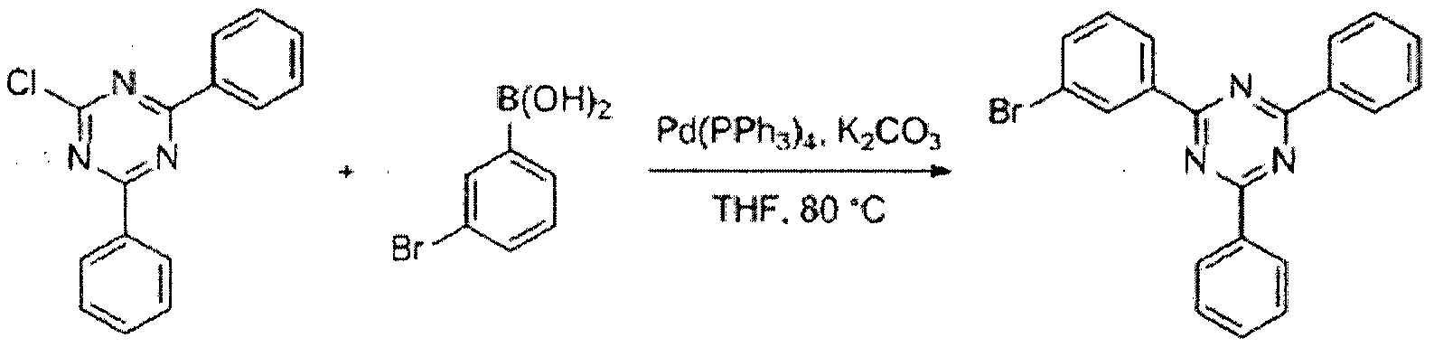
HRMS (70 eV, EI+): m/z calcd for C21H14BrN3: 387.0371, found: 387
Elemental Analysis: C, 65 %; H, 4 % 합성예 2: 중간체 1-2의 합성

f-1 i-2
중간체 1-1과 3-chlorophenyl boronic acid (TCI)을 상기 중간체 1-1의 합성방법과 동일한 방법으로 합성, 정제하여 중간체 1-2 51 g (95 %)을 수득하였다.
HRMS (70 eV, EI+): m/z calcd for C27H,8C1N3: 419.1189, found: 419
Elemental Analysis: C, 77 %; H, 4 % 합성예 3: 중간체 1-3의 합성
[반웅식 3]

질소 환경에서 1-2 (100 g, 238 mmol)을 dimethylforamide(DMF) 1L에 녹인 후, 여기에 bis(pinacolato)diboron (72.5 g, 285 mmol)과 (1,1- bis(diphenylphosphine)ferrocene)dichloropalladium(II) (2 g, 2.38 mmol), 그리고 potassium acetate(58 g, 595 mmol)을 넣고 150°C에서 48시간 동안 가열하여 환류시켰다. 반응 완료 후 반웅액에 물을 넣고 흔합물을 필터한 후, 진공오본에서 건조하였다. 이렇게 얻어진 잔사를 컬럼 크로마토그래피로 분리 정제하여 상기 화합물 1-3(107 g, 88 %)을 얻었다.
HRMS (70 eV, EI+): m/z calcd for C33H30BN3O2: 511.2431 , found: 511
Elemental Analysis: C, 77 %; H, 6 % 합성예 4: 중간체 i-4의 합성
4]

HRMS (70 eV, EI+): m/z calcd for C30H27BO2: 539.0997, found: 539
Elemental Analysis: C, 73.34; H, 4.10 합성예 5: 중간체 1-5의 합성

중간체 1-3의 합성방법과 동일한 방법으로 합성, 정제하여 중간체 1-5 95
%)을 수득하였다.
HRMS (70 eV, EI+): m/z calcd for C39H34BN302: 587.2744, found: 587
Elemental Analysis: C, 80 %; H, 6 % 합성예 6: 중간체 1-6의 합성

질소 환경에서 2-bromo-l,l'-biphenyl (20 g, 85.8 mmol)을 dimethylforamide(DMF) 1L에 녹인 후, 여기에 bis(pinacolato)diboiOn (26 g, 103 mmol)와 (1,1'- bis(diphenylphosphine)ferrocene)dichloropalladium(II)(0.7 g, 0.85 mmol) 그리고 potassium acetate(58 g, 595 mmol)을 넣고 150°C에서 5시간 동안 가열하여 환류시켰다. 반웅 완료 후 반웅액에 물을 넣고 흔합물을 필터한 후, 진공오븐에서 건조하였다. 이렇게 얻어진 잔사를 플래시 컬럼 크로마토그래피로 분리 정제하여 상기 화합물 1-6(19 g, 83 %)을 얻었다.
HRMS (70 eV, EI+): m/z calcd for C18H21 B02: 280.1635, found: 280
Elemental Analysis: C, 77 %; H, 7% 합성예 7: 중간체 1-7의 합성
7]

H MS (70 eV, EI+): m/z calcd for C18H13Br: 308.0201, found: 308 Elemental Analysis: C, 70 %; H, 4 %
합성예 8: 중간체 1-8의 합성

I-8
질소 환경에서 3-bromo-U'-biphenyl (20 g, 85.8 mmol)을 dimethylforamide(DMF) 1L에 녹인 후, 여기에 bis(pinacolato)diboron (26 g, 103 mmol)과 (Ι,Γ- bis(diphenylphosphine)ferrocene)dichloropalladium(II) (0.7 g, 0.85 mmol), 그리고 potassium acetate(58 g, 595 mmol)을 넣고 150°C에서 5시간 동안 가열하여 환류시켰다. 반웅 완료 후 반응액에 물을 넣고 흔합물을 필터한 후, 진공오븐에서 건조하였다. 이렇게 얻어진 잔사를 플래시 컬럼 크로마토그래피로 분리 정제하여 상기 화합물 1-8 (20 g, 85 %)을 얻었다.
HRMS (70 eV, EI+): m/z calcd for C18H21B02: 280.1635, found: 280.
Elemental Analysis: C, 77 %; H, 7 % 합성예 9: 중간체 1-9의 합성

i-a i-9
질소 환경에서 상기 화합물 1-8 (20 g, 71 mmol)을 THF 1 L에 녹인 후, 여기에 1 -bromo-3 -iodobenzene (22 g, 78 mmol, TCI t)과 tetrakis(triphenylphosphine)palladium (0.8 g, 0.71 mmol)을 넣고 교반시켰다. 물에 포화된 potassuim carbonate(25 g, 177 mmol)을 넣고 8( C에서 12시간 동안 가열하여 환류시켰다. 반응 완료 후 반웅액에 물을 넣고 dichloromethane(DCM)로 추출한 다음 무수 MgS04로 수분을 제거한 후, 필터하고 감압 농축하였다. 이렇게 얻어진 잔사를 플래시 컬럼 크로마토그래피로 분리
정제하여 상기 화합물 1-9 (20 g, 91 %)를 얻었다.
HRMS (70 eV, EI+): m/z calcd for C18H13Br: 308.0201, found: 308 Elemental Analysis: C, 70 %; H, 4 % 합성예 10: 중간체 1-10의 합성
10]

질소 환경에서 상기 화합물 1-3 (50 g, 98 mmol)을 THF 1L에 녹인 후, 여기에 1 -bromo-4-iodobenzene (33 g, 117 mmol)과 tetrakis(triphenylphosphine)palladium (1 g, 0.98 mmol)을 넣고 교반시켰다. 물에 포화된 potassuim carbonate(34 g, 245 mmol)을 넣고 80°C에서 12시간 동안 가열하여 환류시켰다. 반응 완료 후 반웅액에 물을 넣고 dichloromethane(DCM)로 추출한 다음 무수 MgS04로 수분을 제거한 후, 필터하고 감압 농축하였다. 이렇게 얻어진 잔사를 플래시 컬럼 크로마토그래피로 분리 정제하여 상기 화합물 1-10(50 g, 95 %)를 얻었다.
HRMS (70 eV, EI+): m/z calcd for C30H27BO2: 539.0997, found: 539 540.
Elemental Analysis: C, 73.34; H, 4.10 합성예 11: 중간체 1-11의 합성
1 1]

질소 환경에서 1-10 (100 g, 185 mmol)을 dimethylforamide(DMF) 1L에 녹인 후, 여기에 bis(pinacolato)diboron (56 g, 222 mmol)과 (Ι,Ι'- bis(diphenylphosphine)ferrocene)dichloropalladium(II) (1.5 g, 1.85 mmol) 그리고 potassium acetate(45 g, 595 mmol)을 넣고 150°C에서 5시간 동안 가열하여 환류 시켰다. 반웅
완료 早 반응액에 물을 넣고 흔합물을 필터한 후, 진공오븐에서 건조하였다. 이렇게 얻어진 잔사를 플래시 컬럼 크로마토그래피로 분리 정제하여 상기 화합물 1-1 1 (95 & 88 %)을 얻었다.
HRMS (70 eV, EI+): m/z calcd for C39H34BN302: 587.2744, found: 587
Elemental Analysis: C, 80 %; H, 6% 합성예 12 내지 16: 중간체 1-12의 합성 (피리딘 코어를 갖는 중간체의 합성 )
[반웅식 12]

1-12
[반웅식 13]


2-chloro-4,6-diphenyl-l,3,5-triazine 대신 4-chloro-2,6-diphenylpyridine(TCI][ct) 사용한 것을 제외하고는, 중간체 1-1 내지 중간체 1-5, 중간체 1-10, 중간체 1-1 1의 합성방법과 동일한 방법으로 합성, 정제하여 중간체 1-12 내지 중간체 1-16을
수득하였다.
HRMS (70 eV, EI+): m/z calcd for C4iH36BN02: 585.2839, found: 585
Elemental Analysis: C, 84 %; H, 6 % 합성예 17 내지 21: 중간체 1-17의 합성 (피리미딘 코어를 갖는 중간체의 합성)
[반응식 17]


2-chloro-4,6-diphenyl- 1 ,3 ,5-triazine 대신 2-chloro-4,6-diphenyl- 1,3- pyrimidine(TCI社)을 사용한 것올 제외하고는, 중간체 1-1 내지 중간체 1-5, 중간체 I- 10, 중간체 1-1 1의 합성방법과 동일한 방법으로 합성, 정제하여 증간체 1-17 내지 중간체 1-21을 수득하였다.
HRMS (70 eV, EI+): m/z calcd for C40H35BN2O2: 586.2792, found: 586
Elemental Analysis: C, 82 %; H, 6 % 합성예 22 내지 26: 중간체 1-22의 합성 (페닐렌 코어를 갖는 중간체의 합성)

!-22
HRMS (70 eV, EI+): m/z calcd for C40H35BN2O2: 586.2792, found: 586
Elemental Analysis: C, 82 %; H, 6 %


반 26

2-chloro-4,6-diphenyl- 1 ,3,5-triazine 대신 4,4'-(5-Bromo-l,3- phenylene)dipyridine (일본 공개특허공보 제 2008-127326호의 합성예 2 참조)을 사용한 것을 제외하고는, 중간체 1-1 내지 중간체 1ᅳ5, 중간체 1-10, 중간체 I-U의 합성방법과 동일한 방법으로 합성, 정제하여 중간체 1-22 내지 증간체 1-26을 수득하였다. 합성예 27: 중간체 1-27의 합성
27]

HRMS (70 eV, EI+): m/z calcd for C39H26BrN3: 615.1310, found 616
Elemental Analysis: C, 76 %; H, 4 % 합성예 28: 중간체 1-28의 합성
28]

HRMS (70 eV, EI+): m/z calcd for C45H3gBN302: 663.3057, found: 663
Elemental Analysis: C, 81 %; H, 6 % 합성예 29: 중간체 1-29의 합성
29]

질소 환경에서 4-bromo-p-terphenyl (50 g, 162 mmol TCI社)을
dimethylforamide(DMF) 1 L에 녹인 후, 여기에 bis(pinacolato)diboron (49 g, 194 mmol)과 (1 ,l '-bis(diphenylphosphine)ferrocene)dichloropalladium(II)(l .3 g, 1.62 mmol) 그리고 potassium acetate(40 g, 405 mmol)을 넣고 150°C에서 12시간 동안 가열하여 환류시켰다. 반응 완료 후 반웅액에 물을 넣고 흔합물을 필터한 후, 진공오븐에서 건조하였다. 이렇게 얻어진 잔사를 플래시 컬럼 크로마토그래피로 분리 정제하여 상기 화합물 I- 29 (47 g, 82 %)을 얻었다.
HRMS (70 eV, EI+): m/z calcd for C24H25B02: 356.1948, found: 356
Elemental Analysis: C, 81 %; H, 7 % 합성예 30: 중간체 1-30의 합성

질소 환경에서 상기 화합물 1-29 (50 g, 140 mmol)을 THF 1L에 녹인 후, 여기에 1 -bromo-4-iodobenzene (47 g, 168 mmol)과 tetrakis(triphenylphosphine)palladium (1.6 g, 1.4 mmol)을 넣고 교반시켰다. 물에 포화된 potassuim carbonate(48 g, 350 mmol)을 넣고 80°C에서 12시간 동안 가열하여 환류시켰다. 반웅 완료 후 반웅액에 물을 넣고 dichloromethane(DCM)로 추출한 다음 무수 MgS04로 수분을 제거한 후, 필터하고 감압 농축하였다. 이렇게 얻어진 잔사를 플래시 컬럼 크로마토그래피로 분리 정제하여 상기 화합물 1-30 (44 g, 89 %)를 얻었다.
HRMS (70 eV, EI+): m/z calcd for C24H17Br: 384.0514, found 384 Elemental Analysis: C, 75 %; H, 4 %
합성예 31: 중간체 1-31의 합성
31 ]

질소 환경에서 1-30 (20 g, 52 mmol)을 dimethylforamide(DMF) 1L에 녹인 후, 여기에 bis(pinacolato)diboron (16 g, 62.5 mmol)과 (Ι ,Γ- bis(diphenylphosphine)ferrocene)dichloropalladium(II)(0.4 g, 0.52 mmol) 그리고 potassium
13 ^ 130 11111 01)을 넣고 150°C에서 5시간 동안 가열하여 환류시켰다. 반웅 완료 후 반응액에 물을 넣고 흔합물을 필터한 후, 진공오본에서 건조하였다. 이렇게 얻어진 잔사를 플래시 컬럼 크로마토그래피로 분리 정제하여 상기 화합물 1-31 (19 g, 85 %)을 얻었다.
HRMS (70 eV, EI+): m/z calcd for C30H29BO2: 432.2261, found: 432
Elemental Analysis: C, 83 %; H, 7 % 합성예 32: 중간체 1-32의 합성
32]

1-32
질소 환경에서 상기 화합물 2-chloro-4,6-diphenyl-l,3,5-triazine (50 g, 187 mmol)을 THF 1L에 녹인 후, 여기에 (4-bromophenyl)boronic acid (45 g, 224.12 mmol, Aldrich社)와 tetrakis(triphenylphosphine)palladium (2.1 g, 1.87 mmol)을 넣고 교반시켰다. 물에 포화된 potassuim carbonate(64 g, 467 mmol)을 넣고 80°C에서 12시간 동안 가열하여 환류시켰다. 반웅 완료 후 반응액에 물올 넣고 dichloromethane(DCM)로
추출한 다음 무수 MgS04로 수분을 제거한 후, 필터하고 감압 농축하였다. 이렇게 얻어진 잔사를 플래시 컬럼 크로마토그래피로 분리 정제하여 상기 화합물 1-32 (70 g, 96 %)를 얻었다.
HRMS (70 eV, EI+): m/z calcd for C2iH,4BrN3: 387.0371, found: 387.
Elemental Analysis: C, 65%; H, 4% 합성예 33: 중간체 1-33의 합성

질소 환경에서 상기 화합물 1-29 (50 g, 140 mmol)을 THF 1L에 녹인 후, 여기에
1 -bromo-3 -iodobenzene (47 g, 168 mmol)과 tetrakis(triphenylphosphine)palladium (1.6 g, 1.4 mmol)을 넣고 교반시켰다. 물에 포화된 potassuim carbonate(48 g, 350 mmol)을 넣고 80°C에서 12시간 동안 가열하여 환류시켰다. 반웅 완료 후 반웅액에 물을 넣고 dichloromethane(DCM)로 추출한 다음 무수 MgS04로 수분을 제거한 후, 필터하고 감압 농축하였다. 이렇게 얻어진 잔사를 폴래시 컬럼 크로마토그래피로 분리 정제하여 상기 화합물 1-33 (46 g, 90 %)를 얻었다.
HRMS (70 eV, EI+): m/z calcd for C24H,7Br: 384.0514, found 384
Elemental Analysis: C, 75 %; H, 4 % 합성예 34: 증간체 1-34의 합성
*

질소 환경에서 1-33 (20 g, 52 mmol)을 dimethylforamide(DMF) 1L에 녹인 후 여기에 bis(pinacolato)diboron (16 g, 62.5 mmol)과 (Ι,Ι'-
bis(diphenylphosphine)ferrocene)dichloropalladium(II)(0.4 g, 0.52 mmol) 그리고 potassium
^^ 13 ^ 130 11^101)을 넣고 150°C에서 5시간 동안 가열하여 환류 시켰다. 반웅 완료 후 반웅액에 물을 넣고 흔합물을 필터한 후, 진공오븐에서 건조하였다. 이렇게 얻어진 잔사를 플래시 컬럼 크로마토그래피로 분리 정제하여 상기 화합물 1-34 (21 g, 83 %)을 얻었다.
HRMS (70 eV, EI+): m/z calcd for C30H29BO2: 432.2261, found: 432
Elemental Analysis: C, 83 %; H, 7 % 합성예 35: 중간체 1-35의 합성

질소 환경에서 상기 화합물 l,3-dibromo-5-chlorobenzene (50 g, 185 mmol, TCI社)을 THF 1 L에 녹인 후, 여기에 naphthalene- 1-boronic acid (32 g, 185 mmol, Aldrich社)와 tetrakis(triphenylphosphine)palladium (2 g, 1.8 mmol)을 넣고 교반시켰다. 물에 포화된 potassuim carbonate(64 g, 462 mmol)을 넣고 80°C에서 12시간 동안 가열하여 환류시켰다. 반웅 완료 후 반응액에 물을 넣고 dichloromethane(DCM)로 추출한 다음 무수 MgS04로 수분을 제거한 후, 필터하고 감압 농축하였다. 이렇게 얻어진 잔사를 플래시 컬럼 크로마토그래피로 분리 정제하여 상기 화합물 1-35 (32 g, 56 %)를 얻었다.
HRMS (70 eV, EI+): m/z calcd for C16Hi0BrCl: 315.9654, found 316
Elemental Analysis: C, 61 %; H, 3 % 합성예 36: 중간체 1-36의 합성
반웅식 36]
질소 환경에서 상기 화합물 1-35 (30 g, 95 mmol)을 THF 1L에 녹인 후, 여기에 phenylboronic acid (14 g, 1 14 mmol, Aldrich社)와 tetrakis(triphenylphosphine)palladium (1 g, 0.95 mmol)을 넣고 교반시켰다. 물에 포화된 potassuim carbonate(33 g, 237 mmol)을 넣고 80 °C에서 12시간 동안 가열하여 환류시켰다. 반응 완료 후 반웅액에 물을 넣고 dichloromethane(DCM)로 추출한 다음 무수 MgS04로 수분을 제거한 후, 필터하고 감압 농축하였다. 이렇게 얻어진 잔사를 플래시 컬럼 크로마토그래피로 분리 정제하여 상기 화합물' 1-36 (32 g, 75 %)를 얻었다.
HRMS (70 eV, EI+): m/z calcd for C22H15C1: 314.0862, found 314
Elemental Analysis: C, 84 %; H, 5 % 합성예 37: 중간체 1-37의 합성
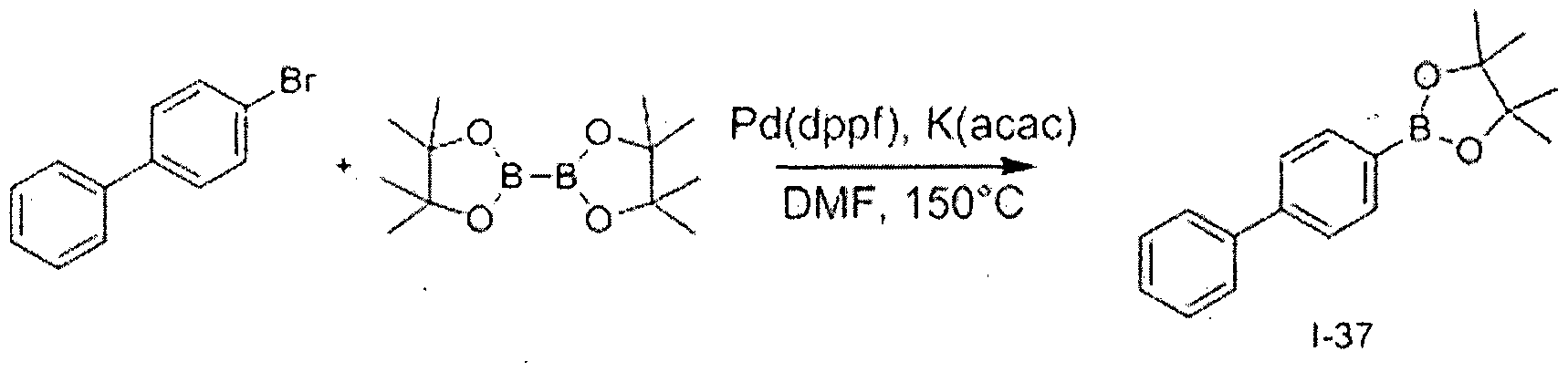
질소 환경에서 4-bromo-U'-biphenyl(20 g, 86 mmol, TCI社)을
dimethylfommide(DMF) 1L에 녹인 후, 여기에 bis(pinacolato)diboron (26 g, 103 mmol)과 (l, -bis(diphenylphosphine)ferrocene)dichloropalladium(II)(0.7 g, 0.86 mmol) 그리고 potassium acetate(21 g, 215 mmol)을 넣고 150°C에서 5시간 동안 가열하여 환류시켰다. 반웅 완료 후 반응액에 물을 넣고 흔합물을 필터한 후, 진공오븐에서 건조하였다. 이렇게 얻어진 잔사를 플래시 컬럼 크로마토그래피로 분리 정제하여 상기 화합물 I- 37 (20 g, 85 %)을 얻었다.
HRMS (70 eV, EI+): m/z calcd for Ci8H21BO2:280.1635, found: 280
Elemental Analysis: C, 77 %; H, 8 % 합성예 38: 증간체 1-38의 합성

HRMS (70 eV, EI+): m/z calcd for C18H13Br:309.1998, found 309 Elemental Analysis: C, 70 %; H, 4 % 합성예 39: 중간체 1-39의 합성
질소 환경에서 1-38(25 g, 81 mmol)을 dimethylforamide(DMF) 1L에 녹인 후, 여기에 bis(pinacolato)diboron (25 g, 97 mmol)과 (Ι,Γ- bis(diphenylphosphine)ferrocene)dichloropalladium(II)(0.7 g, 0.81 mmol) 그리고 potassium acetate(20 g, 203 mmol)을 넣고 150°C에서 5시간 동안 가열하여 환류시켰다. 반웅 완료 후 반웅액에 물을 넣고 흔합물올 필터한 후, 진공오븐에서 건조하였다ᅳ 이렇게 얻어진 잔사를 플래시 컬럼 크로마토그래피로 분리 정제하여 상기 화합물 1-39 (27 g, 93 %)을 얻었다.
HRMS (70 eV, EI+): m/z calcd for C24H25B02:356.1948, found: 356
Elemental Analysis: C, 81 %; H, 7 % 합성예 40: 중간체 1-40의 합성

HRMS (70 eV, EI+): m/z calcd for C24Hi7Br:384.0514, found 384 Elemental Analysis: C, 75 %; H, 4 % 합성예 41: 중간체 1-41의 합성
41]

HRMS (70 eV, EI+): m/z calcd for C30H29BO2:432.2261, found: 432
Elemental Analysis: C, 83 %; H, 7 % 합성예 42: 중간체 1-42의 합성

질소 환경에서 1-48 (27.8 g, 105.00 mmol)을 dimethylforamide(DMF) 1L에 녹인 후, 여기에 bis(pinacolato)diboron (32.0 g, 126.01 mmol)과 (Ι,Ι'- bis(diphenylphosphine)ferrocene)dichloropalladium(II)(0.86 g, 1.05 mmol) 그리고 potassium acetate(25.8 g, 262.51 mmol)을 넣고 150°C에서 5시간 동안 가열하여 환류시켰다.
반응 완료 후 반웅액에 물을 넣고 흔합물을 필터한 후, 진공오본에서 건조하였다. 이렇게 얻어진 잔사를 플래시 컬럼 크로마토그래피로 분리 정제하여 상기 화합물 I- 42 (33 g, 88 %)올 얻었다.
HRMS (70 eV, EI+): m/z calcd for C24H25B02:356.1948, found: 356
Elemental Analysis: C, 81 %; H, 7 % 합성예 43: 중간체 1-43의 합성

HRMS (70 eV, EI+): m/z calcd for C9H5C12N3:224.9861, found: 225
Elemental Analysis: C, 48 %; H, 2 % 합성예 44: 중간체 1-44의 합성
[반응식 44]

질소 환경에서 상기 화합물 1-42(50 g, 140 mmol)을 THF 1L에 녹인 후, 여기에 1-43 (31 g, 140 mmol)과 tetrakis(triphenylphosphine)palladium (1.6 g, 1.4 mmol)을 넣.고 교반시켰다. 물에 포화된 potassuim carbonate(48 g, 350 mmol)을 넣고 80°C에서 12시간 동안 가열하여 환류시켰다. 반응 완료 후 반웅액에 물을 넣고
dichloromethane(DCM)로 추출한 다음 무수 MgS04로 수분을 제거한 후, 필터하고 감압 농축하였다. 이렇게 얻어진 잔사를 플래시 컬럼 크로마토그래피로 분리 정제하여 상기 화합물 1-44 (32 g, 70 %) 얻었다.
HRMS (70 eV, EI+): m/z calcd for C27H18C1N3:419.1 189, found 419 Elemental Analysis: C, 77 %; H, 4 % 합성예 45: 중간체 1-45 및 1-48의 합성

질소 환경에서 상기 화합물 l,3-dibromo-5-chlorobenzene (100 g, 370 mmol, TCI社)을 THF 2L에 녹인 후, 여기에 phenylboronic acid (47.3 g, 388 mmol, Aldrich社)와 tetrakis(triphenylphosphine)palladium (1.5 g, 1.36 mmol)-i: 넣고 교반시켰다. 물에 포화된 potassuim carbonate(127 g, 925 mmol)을 넣고 80°C에서 12시간 동안 가열하여
환류시켰다. 반응 완료 후 반웅액에 물을 넣고 dichloromethane(DCM)로 추출한 다음 무수 MgS04로 수분을 제거한 후, 필터하고 감압 농축하였다. 이렇게 얻어진 잔사를 플래시 컬럼 크로마토그래피로 분리 정제하여 상기 화합물 1-45 (49 g, 50 %)를 얻었다.
HRMS (70 eV, EI+): m/z calcd for C12H8BrCl: 265.9498, found 266 Elemental Analysis:
C, 54 %; H, 3 %
phenyl boronic acid 의 당량을 2배 증가하여 첨가한 것 외에는 같은 방법으로 합성하여 상기 화합물 1-48을 얻었다.
HRMS (70 eV, EI+): m/z calcd for C,8H|3C1: 264.0706, found 264 Elemental Analysis: C, 82 %; H, 5 % 합성예 46: 중간체 1-46의 합성

질소 환경에서 상기 화합물 1-45 (20 g, 75 mmol)을 THF 1L에 녹인 후, 여기에 4-Biphenylboronic acid (17.7 g, 90 mmol, TCI社)와 tetrakis(triphenylphosphine)palladium (863 mg, 0.74 mmol)을 넣고 교반시켰다. 물에 포화된 potassuim carbonate(26 g, 186.87 mmol)을 넣고 8C C에서 12시간 동안 가열하여 환류시켰다. 반웅 완료 후 반응액에
물을 넣고 dichloromethane(DCM)로 추출한 다음 무수 MgS04로 수분을 제거한 후, 필터하고 감압 농축하였다. 이렇게 얻어진 잔사를 플래시 컬럼 크로마토그래피로 분리 정제하여 상기 화합물 1-46 (49 g, 80 %)를 얻었다.
HRMS (70 eV, EI+): m/z calcd for C24Hl7Cl: 340.1019, found 340 Elemental Analysis: C, 85 %; H, 5 % 합성예 47: 중간체 1-47의 합성

HRMS (70 eV, EI+): m/z calcd for C3oH29B02: 432.2261, found: 432
Elemental Analysis: C, 83 %; H, 7 % 최종 화합물의 합성
합성예 49: 화합물 A-1의 합성
49]

질소 환경에서 상기 화합물 1-5(20 g, 34 mmol)을 tetrahydrofuran(THF) 0.2L에
녹인 후, 여기에 3-Biphenylboronic acid (9.5 g, 40 mrnol, TCI社)와
tetmkis(triphenylphosphine)palladium(0.39 g, 0.34 mmol)을 넣고 교반시켰다. 물에 포화된 potassuim carbonate(12 g, 85 mmol)을 넣고 80°C에서 20시간 동안 가열하여 환류시켰다. 반응 완료 후 반응액에 물을 넣고 dichloromethane(DCM)로 추출한 다음 무수
MgS04로 수분을 제거한 후, 필터하고 감압 농축하였다. 이렇게 얻어진 잔사를 플래시 컬럼 크로마토그래피로 분리 정제하여 상기 화합물 A-l(24 g, 70 %)을 얻었다. 화합물 A-1의 분자량은 613.2518이다.
HRMS (70 eV, EI+): m/z calcd for C45H3 IN3: 613.2518, found: 613 Elemental Analysis: C, 88 %; H, 5 % 합성예 50: 화합물 B-l의 합성

질소 환경에서 상기 화합물 1-16(20 g, 34 mmol)을 tetmhydrofuran(THF) 0.2L에 녹인 후, 여기에 3-bromo-l,l'-biphenyl (9.5 g, 40 mmol)과
tetrakis(triphenylphosphine)palladium(0.39 g, 0 4 mmol)을 넣고 교반시켰다. 물에 포화된 !^&^ 11 &1¾0 { 12 85 11111101)을 넣고 80°C에서 20시간 동안 가열하여 환류시켰다. 반응 완료 후 반웅액에 물을 넣고 dichloromethane(DCM)로 추출한 다음 무수
MgS04로 수분을 제거한 후, 필터하고 감압 농축하였다. 이렇게 얻어진 잔사를 플래시 컬럼 크로마토그래피로 분리 정제하여 상기 화합물 B-l(15 g, 72 %)을 얻었다. 화합물 B-1의 분자량은 61 1.2613 이다.
HRMS (70 eV, EI+): m/z calcd for C47H33N: 611.2613, found: 611
Elemental Analysis: C, 92 %; H, 5 % 합성예 51: 화합물 B-2의 합성
51]

질소 환경에서 상기 화합물 1-21(20 g, 34 mmol)을 tetrahydrofuran(THF)
 녹인 후, 여기에 3-bromo-l,l'-biphenyl (9.5 g, 40 mmol)과
tetrakis(triphenylphosphine)palladium(0.39 g, 0.34 mmol) 넣고 교반시켰다. 물에 포화된
5^111^&1:130 ^ 12 £, 85 ^01)을 넣고 80 °C에서 20시간 동안 가열하여 환류시켰다. 반웅 완료 후 반응액에 물을 넣고 dichloromethane(DCM)로 추출한 다음 무수
MgS04로 수분을 제거한 후, 필터하고 감압 농축하였다. 이렇게 얻어진 잔사를 풀래시 컬럼 크로마토그래피로 분리 정제하여 상기 화합물 B-2(16 g, 75 %)을 얻었다. 화합물 B-2의 분자량은 612.2565이다.
HRMS (70 eV, EI+): m/z calcd for C46H32N2: 612.2565, found: 612
Elemental Analysis: C, 90 %; H, 5 % 합성예 52: 화합물 A-2의 합성
2]

689.2831이다.
HRMS (70 eV, EI+): m/z calcd for C51H35N3: 689.2831, found: 689
Elemental Analysis: C, 89 %; H, 5 %
합성예 53: 화합물 A-3의 합성
53]

613.2518이다.
HRMS (70 eV, EI+): m/z calcd for C45H31N3: 613.2518, found: 613
Elemental Analysis: C, 88 %; H, 5 % 합성예 54: 화합물 A-4의 합성

689.2831이다.
HRMS (70 eV, EI+): m/z calcd for C5iH35N3: 689.2831, found: 689.
Elemental Analysis: C, 89 %; H, 5 % 합성예 55: 화합물 A-5의 합성

689.2831이다.
HRMS (70 eV, EI+): m/z calcd for C51H35N3: 689.2831, found: 689.
Elemental Analysis: C, 89 %; H, 5 % 합성예 56: 화합물 A-8의 합성

HRMS (70 eV, EI+): m/z calcd for C45¾iN3: 613.2518, found: 613
Elemental Analysis: C, 88 %; H, 5 % 합성예 57: 화합물 A-9의 합성

질소 환경에서 상기 화합물 1-3(20 g, 39 mmol)을 tetrahydrofuran(THF) 0.2L에 녹인 후, 여기에 4-bromo-p-terphenyl (14.5 g, 47 mmol, TCI社)과
tetrakis(triphenylphosphine)palladium(0.45 g, 0.39 mmol)을 넣고 교반시켰다. 물에 포화된 potassuim carbonate(13.5 g, 97 mmol)올 넣고 80 °C에서 20시간 동안 가열하여
환류시켰다. 반웅 완료 후 반응액에 물을 넣고 dichloromethane(DCM)로 추출한 다음 무수 MgS04로 수분올 제거한 후, 필터하고 감압 농축하였다. 이렇게 얻어진 잔사를 플래시 컬럼 크로마토그래피로 분리 정제하여 상기 화합물 A-9 (19 g, 79 %)을 얻었다. 화합물 A-9의 분자량은 613.2518 이다.
HRMS (70 eV, EI+): m/z calcd for C45H3,N3: 613.2518, found: 613
Elemental Analysis: C, 88 %; H, 5 % 합성예 58: 화합물 A-6의 합성

dichloromethane(DCM)로 추출한 다음 무수 MgS04로 수분을 제거한 후, 필터하고 감압 농축하였다. 이렇게 얻어진 잔사를 플래시 컬럼 크로마토그래피로 분리 정제하여 상기 화합물 A-6(32 g, 80 %)를 얻었다. 화합물 A-6의 분자량은
689.2831이다.
HRMS (70 eV, EI+): m/z calcd for C5iH35N3:689.2831, found 689 Elemental Analysis: C, 89 %; H, 5 % 합성예 59: 화합물 A-72의 합성
59]

질소 환경에서 상기 화합물 1-3(20 g, 39 mmol)을 tetrahydrofuran(THF) 0.2L에 녹인 후, 여기에 3- 01110-1,1'- 1)11^ 1(11 4711^101)과
tetrakis(triphenylphosphine)palladium(0.45 g, 0.39 mmol)을 넣고 교반시켰다. 물에 포화된 !^&5^^0&1¾0 1^13.5 971 101)을 넣고 80°C에서 20시간 동안 가열하여
환류시켰다. 반응 완료 후 반웅액에 물을 넣고 dichloromethane(DCM)로 추출한 다음 무수 MgS04로 수분을 제거한 후, 필터하고 감압 농축하였다. 이렇게 얻어진 잔사를 플래시 컬럼 크로마토그래피로 분리 정제하여 상기 화합물 A-72(16g,78%)을 얻었다. 화합물 A-72의 분자량은 537.2205 이다.
HRMS (70 eV, EI+): m/z calcd for C39H27N3: 537.2205, found: 537
Elemental Analysis: C, 87 %; H, 5 % 합성예 60: 화합물 A-73의 합성

mmol)을 넣고 교반시켰다. 물에 포화된 potassuim carbonate( 10 g, 75 mmol)을 넣고 80 °C에서 20시간 동안 가열하여 환류시켰다. 반웅 완료 후 반웅액에 물을 넣고 dichloromethane(DCM)로 추출한 다음 무수 MgS04로 수분을 제거한 후, 필터하고 감압 농축하였다. 이렇게 얻어진 잔사를 플래시 컬럼 크로마토그래피로 분리 정제하여 상기 화합물 A-73 (14.5 g, 70 %)을 얻었다. 화합물 A-73의 분자량은
765.3144 이다.
HRMS (70 eV, EI+): m/z calcd for C51H35N3: 765.3144, found: 765
Elemental Analysis: C, 89 %; H, 5 % 합성예 61 : 화합물 A-74의 합성

0.51 mmol)을 넣고 교반시켰다. 물에 포화된 potassuim carbonate( 17.5 g, 127 mmol)을 넣고 80°C에서 20시간 동안 가열하여 환류시켰다. 반웅 완료 후 반응액에 물을 넣고 dichloromethane(DCM)로 추출한 다음 무수 MgS04로 수분을 제거한 후, 필터하고
감압 농축하였다. 이렇게 얻어진 잔사를 플래시 컬럼 크로마토그래피로 분리 정제하여 상기 화합물 A-74 (22.5 g, 75 %)을 얻었다. 화합물 A-74의 분자량은
613.2518 이다.
HRMS (70 eV, EI+): m/z calcd for C45H31N3: 613.2518, found: 613.
Elemental Analysis: C, 88 %; H, 5 % 합성예 62: 화합물 A-19의 합성

4,4,5,5-tetramethyl-l,3,2-dioxaborolane 18.12g (50.87 mmol), potassuim carbonate 7.64g (55.30 mmol), Tetrakis(triphenyl phosphine) palladium(O) 1.28g (1.1 1 mmol)올
tetrahydrofuran(THF) lOOmL, 물 30 mL에 넣어준 후, 질소 기류 하에서 10시간 동안 가열하여 환류하였다. 이로부터 수득한 흔합물올 메탄올 500mL에 가하여 결정화된 고형분을 여과한 후, 모노클로로벤젠에 녹여 실리카겔 /셀라이트로 여과하고, 유기 용매를 적당량 제거한 후, 메탄을로 재결정하여 화합물 A-19 (1 1.3g, 83%의 수율)을 수득하였다. 생성된 화합물 A-19의 원소 분석 결과는 하기와 같다.
calcd C45H31N3: C, 88.06; H, 5.09; N, 6.85; found: C, 87.94; H, 5.12; N, 6.76;

250mL 플라스크에 중간체 1-43 5.0g (22.12 mmol), 1-42 18.12g (50.87 mmol):
potassuim carbonate 7.64g (55.30 mmol), Tetrakis(triphenyl phosphine) palladium(O) 1.28g (U l mmol)을 tetrahydrofuran(THF) lOOmL, 물 30 mL에 넣어준 후, 질소 기류 하에서 10시간 동안 가열하여 환류하였다. 이로부터 수득한 흔합물을 메탄을 500mL에 가하여 결정화된 고형분을 여과한 후, 모노클로로벤젠에 녹여 실리카겔 /샐라이트로 여과하고, 유기 용매를 적당량 제거한 후, 메탄올로 재결정하여 화합물 A-20 (8.5.g, 63%의 수율)을 수득하였다. 생성된 화합물 A-20의 원소 분석 결과는 하기와 같다. calcd. C45H3iN3: C, 88.06; H, 5.09; N, 6.85; found: C, 88.16; H, 5.23; N, 6.63; 합성예 64: 화합물 A-23의 합성

250mL 플라스크에 중간체 1-46 5.0g (22.12 mmol), 4,4,5,5-tetmmethyl-2-(5'-phenyl- [ 1 , 1 ':3', 1 "-terphenyl]-3-yl)- 1 ,3,2-dioxaborolane 21.99g (46.60 mmol), potassuim carbonate 7.64g (55.30 mmol), Tetrakis(triphenyl phosphine) palladium(O) 1.28g (1.1 1 mmol)을
tetrahydrofuran(THF) lOOmL, 물 30 mL에 넣어준 후, 질소 기류 하에서 10시간 동안 가열하여 환류하였다. 이로부터 수득한 흔합물을 메탄올 500mL에 가하여 결정화된 고형분을 여과한 후, 모노클로로벤젠에 녹여 실리카겔 /셀라이트로 여과하고, 유기 용매를 적당량 제거한 후, 메탄올로 재결정하여 화합물 A-23 (13.0g, 77%의 수율)을 수득하였다. 생성된 화합물 A-23의 원소 분석 결과는 하기와 같다.
calcd. C57H39N3: C, 89.38; H, 5.13; N, 5.49; found: C, 89.21 ; H, 5.04; N, 5.53; 합성예 65: 화합물 A-25의 합성

250mL 플라스크에 중간체 1-43 5.0g (22.12 mmol), 2-([1,Γ:3',Γ:4",Γ'-
quate henyl]-4-yl)-4,4,5,5-tetramethyl-l,3,2-dioxaborolane 21.99g (46.60 mmol), potassuim carbonate 7.64g (55.30 mmol), Tetrakis(triphenyl phosphine) palladium(O) 1.28g (1.1 1 mmol)을 tetrahydrofuran(THF) lOOmL, 물 30 mL에 넣어준 후, 질소 기류 하에서 10시간 동안 가열하여 환류하였다. 이로부터 수득한 흔합물을 메탄올 500mL에 가하여 결정화된 고형분을 여과한 후, 모노클로로벤젠에 녹여 실리카겔 /셀라이트로 여과하고, 유기 용매를 적당량 제거한 후, 메탄올로 재결정하여 화합물 A-25 (14.2g, 84%의 수율)을 수득하였다. 생성된 화합물 A-25의 원소 분석 결과는 하기와 같다.
calcd. C57H39N3: C, 89.38; H, 5.13; N, 5.49; found: C, 89.48; H, 5.33; N, 5.41 ; 합성예 66: 화합물 A-43의 합성

250mL 플라스크에 중간체 1-43 5.0g (22.12 mmol), 2-([1,1*:3',1":3",1'"- quaterphenyl]-3-yl)-4,4,5,5-tetramethyl-l,3,2-dioxaborolane 21.99g (46.60 mmol), potassuim carbonate 7.64g (55.30 mmol), Tetrakis(triphenyl phosphine) palladium(O) 1.28g (1.11 mmol)을 tetrahydrofuran(THF) lOOmL, 물 30 mL에 넣어준 후, 질소 기류 하에서 10시간 동안 가열하여 환류하였다. 이로부터 수득한 흔합물을 메탄올 500mL에 가하여 결정화된 고형분을 여과한 후, 모노클로로벤젠에 ,녹여 실리카겔 /셀라이트로 여과하고, 유기 용매를 적당량 제거한 후, 메탄을로 재결정하여 화합물 A-43 (12.2g, 72%의 수율)을 수득하였다. 생성된 화합물 A-43의 원소 분석 결과는 하기와 같다.
calcd. C57H39N3: C, 89.38; H, 5.13; N, 5.49; found: C, 89.71 ; H, 5.46; N, 5.24; 합성예 67: 화합물 A-68의 합성
[반응식 67]

질소 환경에서 상기 화합물 1-2 (20 g, 47.63 mmol)을 tetrahydrofuran(THF) 0.2 L에 녹인 후, 여기에 화합물 1-47 (24.71 g, 57.16 mmol)과
tetrakis(triphenylphosphine)palladium(0.55 g, 0.48 mmol)올 넣고 교반시켰다. 물에 포화된 1^&3^11^^1 00 6(13 97 1 1 01)을 넣고 80 °C에서 20시간 동안 가열하여 환류시켰다. 반웅 완료 후 반응액에 물을 넣고 dichloromethane(DCM)로 추출한 다음 무수
MgS04로 수분을 제거한 후, 필터하고 감압 농축하였다. 이렇게 얻어진 잔사를 플래시 컬럼 크로마토그래피로 분리 정제하여 상기 화합물 A-68 (23.66 g, 72 %)을 얻었다. 화합물 A-68의 분자량은 689.86 이다.
HRMS (70 eV, EI+): m/z calcd for C5,H35N3: 689.28, found: 689
Elemental Analysis: C, 89 %; H, 5 % 제 2 화합물의 합성
합성예 68: 중간체 PI-1의 합성
[반웅식 68]

출발 물질인 9H-carbazole (60.00g, 358.83mmol)을 둥근바닥플라스크에
nitrobenzene으로 녹인 후, 4-bromo-4'-iodo- 1 , 1 '-biphenyl (154.58g, 430.60mmol), Na2S04 (50.95g, 358.83mmol), K2C03 (49.52g, 358.83mmol), Cu (6.84g, 107.65mmol) 를 첨가하고 200°C에서 교반하였다. 반응이 완료된 것올 TLC로 확인 후, 감압증류를 통해 nitrobenzene을 제거하고 CH2C12와 물로 추출하였다. 유기층을 MgS04로 건조하고 농축한 후 생성된 화합물을 silica gel column 및 재결정하여 PI-1 104.33g (261.95mmol 수율: 73%) 를 얻었다.
H MS (70 eV, EI+): m/z calcd for C24H,6BrN: 397.05, found: 397
Elemental Analysis: C, 72 %; H, 4 % 합성예 69: 중간체 PI-2의 합성
[반응식 69]

HRMS (70 eV, EI+): m/z calcd for C24Hl9N: 321.15, found: 321
Elemental Analysis: C, 90 %; H, 6 % 합성예 70: 화합물 P-17의 합성

상기 합성에서 얻어진 PI-l(53.59g, 134.06mmol)을 등근바닥플라스크에 toluene으로 녹인 후에 , PI-2(51.71g, 160.87mmol), Pd2(dba)3 (4.59g, 5.0mmol), 50% P(t-Bu)
(4.92ml, 10.0mmol), NaOt-Bu (61.84g, 643.47mmol)을 첨가하고 100°C에서 교반하였다. 반응이 완료된 것을 TLC로 확인후 CH2C12와 물로 추출한 후 유기층을 MgS04로 건조하고 농축한 후 생성된 화합물을 silica-gel column 및 재결정하여 생성물인 P-17 71.08g (1 11.27mmol, 수율: 83%)을 얻었다.
HRMS (70 eV, EI+): m/z calcd for C48H34N2: 638.27, found: 638
Elemental Analysis: C, 90 %; H, 5 % 유기 발광 소자의 제작
실시예 1
ΠΌ (Indium tin oxide)가 1500A의 두께로 박막 코팅된 유리 기판을 증류수 초음파로 세척하였다. 증류수 세척이 끝나면 이소프로필 알코을, 아세톤, 메탄올 등의 용제로 초음파 세척을 하고 건조시킨 후 플라즈마 세정기로 이송시킨 다음 산소 플라즈마를 이용하여 상기 기판올 10분간 세정 한 후 진공 층착기로 기판을 이송하였다. 이렇게 준비된 ITO 투명 전극을 양극으로 사용하여 ITO 기판 상부에 Ν4,Ν4'-디페닐 -Ν4,Ν4'-비스 (9-페닐 -9Η-카바졸 -3-일)바이페닐 -4,4'-디아민 (N4,N4'-diphenyl- N4,N4'-bis(9-phenyl-9H-carbazol-3-yl)biphenyl-4,4'-diamine)(화합물 A)를 진공 증착하여 700A두께의 정공 주입층을 형성하고 상기 정공 주입층 상부에 1,4,5,8,9,1 1- 핵사아자트리페닐렌 -핵사카보니트릴 (1,4,5,8,9,11-hexaazatriphenylene-hexacarbonitrile, HAT-CN)(화합물 B)를 50 A의 두께로 증착한 후 , N- (바이페닐 -4-일) -9,9-디메틸 -N-(4-(9- 페닐 -9H-카바졸 -3-일)페닐) -9H-플루오렌 -2-아민 (N-(biphenyl-4-yl)-9,9-dimethyl-N-(4-(9- phenyl-9H-carbazol-3-yl)phenyl)-9H-fluoren-2-amine)(화합물 C)를 700A의 두께로 증착하여 정공수송층을 형성하였다. 정공수송층 상부에 합성예 70에서 얻어진 화합물 P-17을 진공 증착으로 50A 두께의 정공수송보조층올 형성하였다. 이어서 상기 정공수송보조층 상부에 청색형광 발광 호스트 및 도편트로 SFC社에서
판매하고 있는 BH1 13 과 BD370을 5wt0/。로 도핑하여 200 A의 두께로 증착하여 발광층을 형성하였다.. 이어서 상기 발광층 상부에 합성예 65에서 얻어진 화합물 61을 진공 증착으로 50 A 두께의 전자수송보조층을 형성하였다.
이어서 상기 전자수송보조층 상부에 8-(4-(4- (나프탈렌 -2-일) -6- (나프탈렌 -3-일) - 1 ,3,5-트리아진 -2-일)페닐)퀴놀린 (8-(4-(4-(naphthalen-2-yl)-6-(naphthalen-3-yl)- ,5-triazhi- 2-yl)phenyl)quinoline) (화합물 E)와 Liq(8-hydroxyquinolatolithium)를 동시에 1 : 1 비율로
진공 증착하여 310A 두께의 전자수송층을 형성하고 상기 전자수송층 상부에 Liq 15 A과 A1 1200A을 순차적으로 진공 증착하여 음극을 형성함으로써 유기발광소자를 제작하였다.
상기 유기발광소자는 6층의 유기 박막층을 가지는 구조로 되어 있으며, 구체적으로 nO/A(700A/B(50A/C(700A/정공수송보조층 [P-17(50A)]
/EML[BH113:BD370(95:5wt%)](200A)/전자수송보조층 [화합물 61 (50 A]/
E:Liq=l :l(310A)/ Liq(15 A/Al(1200A)의 구조로 제작하였다. 실시예 2
전자수송보조층에 화합물 61 대신 합성예 67에서 얻어진 화합물 152를 사용한 것을 제외하고는 실시예 1과 동일한 방법으로 유기발광소자를 제작하였다. 참고예 1
정공수송보조층을 형성하지 않고, '화합물 C를 750A의 두께로 증착하여 정공수송층을 형성한 것을 제외하고는 실시예 1과 동일한 방법으로 유기발광소자를 제작하였다. 비교예 1
정공수송보조층을 형성하지 않고, 화합물 C를 750A의 두께로 증착하여 형성하고, 전자수송보조층을 형성하지 않고, 전자수송층에 화합물 E:Liq=l :l(310A) 대신 화합물 E:Liq=l:l(360A) 증착한 것을 제외하고는 실시예 1과 동일한 방법으로 유기발광소자를 제작하였다. 비교예 2
전자수송보조층을 형성하지 않고, 전자수송층에 화합물 E:Liq=l :l(310A) 대신 화합물 E:Liq=l :l(360A) 증착한 것을.제외하고는 실시예 1과 동일한 방법으로 유기발광소자를 제작하였다. 평가
실시예 1, 실시예 2, 참고예 1, 비교예 1 및 비교예 2에 따른 유기발광소자의
발광효율 등을 평가하였다.
구체적인 측정방법은 하기와 같고, 그 결과는 표 1과 같다.
(1) 전압변화에 따른 전류밀도의 변화 측정
제조된 유기발광소자에 대해, 전압을 0V부터 10V까지 상승시키면서 전류- 전압계 (Keithley 2400)를 이용하여 단위소자에 흐르는 전류값을 측정하고, 측정된 전류값을 면적으로 나누어 결과를 얻었다.
(2) 전압변화에 따른 휘도변화 측정
제조된 유기발광소자에 대해, 전압을 0V부터 10V까지 상승시키면서 휘도계 (Minolta Cs-IOOOA)를 이용하여 그 때의 휘도를 측정하여 결과를 얻었다.
(3) 발광효율 측정
상기 (1) 및 (2)로부터 측정된 휘도와 전류밀도 및 전압을 이용하여 동일' 전류밀도 (10 mA/cm2)의 전류 효율 (cd/A) 을 계산하였다.
(4) Roll-off 측정
상기 (3)의 특성수치 중 (Max 수치 - 6000 cd/m2일 때의 수치 / Max 수치)로 계산하여 효율의 하락폭올 0/。로 계산하였다
【표 1】

20: 캐소드
31 : 정공수송층
33 : 정공수송보조 ^
35 : 전자수송보조
37: 정공주입층
Claims
【청구항 1 ]
서로 마주하는 애노드와 캐소드,
상기 애노드와 상기 캐소드 사이에 위치하는 발광층,
상기 애노드와 상기 발광층 사이에 위치하는 정공수송층,
상기 정공수송층과 상기 발광층 사이에 위치하는 정공수송보조층,
상기 캐소드와 상기 발광층 사이에 위치하는 전자수송층, 그리고
상기 전자수송층과 상기 발광층 사이에 위치하는 전자수송보조층을 포함하고, 상기 전자수송보조층은 하기 화학식 1로 표현되는 적어도 1종의 제 1 화합물을 포함하고,
상기 정공수송보조층은 하기 화학식 2로 표현되는 적어도 1종의 제 2 화합물을 포함하는 유기 광전자 소자:

상기 화학식 1에서,
Z는 각각 독립적으로 N, C 또는 CRa이고,
Z 중 적어도 하나는 N 이고,
R1 내지 R6 및 Ra는 각각 독립적으로 수소, 중수소, 치환 또는 비치환된 C1 내지 C10 알킬기, 치환 또는 비치환된 C6 내지 C30 아릴기, 치환 또는 비치환된 C3내지 C30 헤테로아릴기 또는 이들의 조합이고,
L1 내지 L6은 각각 독립적으로 단일결합, 치환 또는 비치환된 C6 내지 C30 아릴렌기, 치환 또는 비치환된 헤테로아릴렌기 또는 이들의 조합이고,
si 내지 s6는 각각 독립적으로 0 내지 5의 정수이고,
2]

상기 화학식 2에서,
R10 내지 R19는 각각 독립적으로 수소, 중수소, 치환 또는 비치환된 C6 내지 C30 아릴기, 치환 또는 비치환된 C2 내지 C30 헤테로아릴기 또는 이들의 조합이고:
L7은 치환 또는 비치환된 C2 내지 C10 알케닐렌기, 치환 또는 비치환된 C6 내지 C30 아릴렌기, 치환 또는 비치환된 C2 내지 C30 헤테로아릴기 또는 이들의 조합이다.
(상기 "치환' '은 적어도 하나의 수소가 중수소, 할로겐기, 히드록시기, 아미노기 , 치환 또는 비치환된 C1 내지 C30 아민기, 니트로기 , 치환 또는 비치환된 C1 내지 C40 실릴기, C1 내지 C30 알킬기, C3 내지 C30 시클로알킬기, C2 내지 C30 헤테로시클로알킬기, C6 내지 C30 아릴기, C2 내지 C30 헤테로아릴기, C1 내지 C20 알콕시기, 플루오로기, C1 내지 C 10 트리플루오로알킬기, 플루오레닐기 또는 시아노기로 치환된 것을 의미한다)
【청구항 2】
제 1항에서
상기 제 1 화합물은 하기 화학식 1 -i 내지 화학식 1-ix 중 어느 하나로 표현되는 유기 광전자 소자:
[화학식 1-i]


[화학식 1-iv
 [화학식 l-v


 [화학식 1-ix]

상기 화학식 1-i에서,
Ral 및 R32는 각각 독립적으로 치환 또는 비치환된 C1 내지 C10 알킬기, 치환 또는 비치환된 C6 내지 C30 아릴기, 치환 또는 비치환된 C2 내지 C30 헤테로아릴기 또는 이들의 조합이고,
nl 및 n2는 각각 독립적으로 0 또는 1의 정수이고, 단 , nl 및 n2는 동시에 0이 아니고,
상기 화학식 1-ii에서,
Rbl 내지 Rb6은 각각 독립적으로 치환 또는 비치환된 C1 내지 C10 알킬기 치환 또는 비치환된 C6 내지 C30 아릴기, 치환 또는 비치환된 C2 내지 C30 헤테로아릴기 또는 이들의 조합이고,
n3 내지 n8은 각각 독립적으로 0 또는 1의 정수이고, 단 , n3 내지 n5는 동시에 0이 아니고 , n6 내지 n8은 동시에 0이 아니고,
상기 화학식 1-iii에서,
Rcl 내지 Rc4는 각각 독립적으로 치환 또는 비치환된 C1 내지 C10 알킬기 치환 또는 비치환된 C6 내지 C30 아릴기, 치환 또는 비치환된 C2 내지 C30 헤테로아릴기 또는 이들의 조합이고,
n9 내지 nl2는 각각 독립적으로 0 또는 1의 정수이고,
상기 화학식 1-iv에서,
Rdi 내지 은 각각 독립적으로 치환 또는 비치환된 C1 내지 C10 알킬기 치환 또는 비치환된 C6 내지 C30 아릴기, 치환 또는 비치환된 C2 내지 C30 헤테로아릴기 또는 이들의 조합이고,
n!3 내지 n20은 각각 독립적으로 0 또는 1의 정수이고,
상기 화학식 1 ^에서,
Xa 내지 Xf는 각각 독립적으로 N 또는 CH이고,
Xa 내지 Xc 중 적어도 하나는 N이고,
Xd 내지 Xf 중 적어도 하나는 N이고,
Rel 내지 Re6은 각각 독립적으로 치환 또는 비치환된 C1 내지 C10 알킬기, 치환 또는 비치환된 C6 내지 C30 아릴기, 치환 또는 비치환된 C2 내지 C30 헤테로아릴기 또는 이들의 조합이고,
n21 내지 n26, ml 및 m2는 각각 독립적으로 0 또는 1의 정수이고, 상기 화학식 1-vi에서,
fl 내지 Rf6은 각각 독립적으로 치환 또는 비치환된 C1 내지 C10 알킬기, 치환 또는 비치환된 C6 내지 C30 아릴기, 치환 ^는 비치환된 C2 내지 C30 헤테로아릴기 또는 이들의 조합이고,
n27 내지 n32는 각각 독립적으로 0 또는 1의 정수이고, 단 , n27 내지 n29는 동시에 0이 아니고 , n30 내지 n32는 동시에 0이 아니고,
상기 화학식 Ι-vii에서,
Xg 내지 X1은 각각 독립적으로 N 또는 CH이고,
Xs 내지 X1 중 적어도 하나는 N이고,
X' 내지 X' 중 적어도 하나는 N이고,
Rgi 및 Rg2는 각각 독립적으로 치환 또는 비치환된 C1 내지 C10 알킬기, 치환 또는 비치환된 C6 내지 C30 아릴기, 치환 또는 비치환된 C2 내지 C30 헤테로아릴기 또는 이들의 조합이고,
n33 및 n34는 각각 독립적으로 0 또는 1의 정수이고,
상기 화학식 1 -viii에서,
Rhl 내지 Rh6는 각각 독립적으로 치환 또는 비치환된 C1 내지 C10 알킬기, 치환 또는 비치환된 C6 내지 C30 아릴기, 치환 또는 비치환된 C2 내지 C30 헤테로아릴기 또는 이들의 조합이고,
n35 내지 n40은 각각 독립적으로 0 또는 1의 정수이고,
상기 화학식 1-ix에서,
R" 내지 R13은 각각 독립적으로 치환 또는 비치환된 C1 내지 C10 알킬기, 치환 또는 비치환된 C6 내지 C30 아릴기, 치환 또는 비치환된 C2 내지 C30
헤테로아릴기 또는 이들의 조합이고,
n41 내지 n43은 각각 독립적으로 0 또는 1의 정수이며,
상기 화학식 1-i 내지 l-v, 및 1-ix 에서, X1 내지 X9 은 CH 또는 N 이며, 상기 X' 내지 X9 중 적어도 하나는 N 이며,
상기 화학식 1-vi, 1-vii 및 1-viii 에서, X1 내지 X3은 CH 또는 N이며, 상기 X1 내지 X3 중 적어도 하나는 N 이다.
(상기 "치환 "은 적어도 하나의 수소가 중수소, 할로겐기, 히드록시기, 아미노기, 치환 또는 비치환된 C1 내지 C30 아민기, 니트로기, 치환 또는 비치환된 C1 내지 C40 실릴기, C1 내지 C30 알킬기, C3 내지 C30 시클로알킬기, C2 내지 C30 헤테로시클로알킬기, C6 내지 C30 아릴기, C2 내지 C30 헤테로아릴기, C1 내지 C20 알콕시기, 플루오로기, C1 내지 C10 트리플루오로알킬기, 플루오레닐기 또는 시아노기로 치환된 것을 의미한다)
【청구항 3】
제 1항에서,
상기 게 1 화합물은 하기 화학식 Y로 표현되는 유기 광전자 소자:
γ]

상기 화학식 γ에서,
Z는 각각 독립적으로 N 또는 CH이고,
Z 중 적어도 하나는 N 이고,
R1 내지 R6은 각각 독립적으로 수소, 중수소, 치환 또는 비치환된 C1 내지 C10 알킬기, 치환 또는 비치환된 C6 내지 C30 아릴기, 치환 또는 비치환된 C3내 C30 헤테로아릴기 또는 이들의 조합이고,
L1 내지 L6는 각각 독립적으로 단일결합, 치환 또는 비치환된 C6 내지 C30
아릴렌기, 치환 또는 비치환된 헤테로아릴렌기 또는 이들의 조합이고, sl 내지 s6는 각각 독립적으로 0 내지 5의 정수이다.
(상기 "치환 "은 적어도 하나의 수소가 중수소, 할로겐기, 히드록시기, 아미노기, 치환 또는 비치환된 C1 내지 C30 아민기, 니트로기, 치환 또는 비치환된 C1 내지 C40 실릴기, C1 내지 C30 알킬기, C3 내지 C30 시클로알킬기, C2 내지 C30 해테로시클로알킬기, C6 내지 C30 아릴기, C2 내지 C30 헤테로아릴기, C1 내지 C20 알콕시기, 플루오로기, C1 내지 C10 트리플루오로알킬기, 플루오레닐기 또는 시아노기로 치환된 것을 의미한다)
【청구항 4】
게 1항에서,
상기 제 1 화합물은 하기 화학식 Z로 표현되는 유기 광전자 소자:

상기 화학식 z에서,
Z는 각각 독립적으로 N 또는 CH이고,
Z 중 적어도 하나는 N 이고,
R1 내지 R6은 각각 독립적으로 수소, 중수소, 치환 또는 비치환된 C1 내지 C10 알킬기, 치환 또는 비치환된 C6 내지 C30 아릴기, 치환 또는 비치환된 C3내지 C30 헤테로아릴기 또는 이들의 조합이고,
L1 내지 L6는 각각 독립적으로 단일결합, 치환 또는 비치환된 C6 내지 C30 아릴렌기, 치환 또는 비치환된 해테로아릴렌기 또는 이들의 조합이고,
sl 내지 s6는 각각 독립적으로 0 내지 5의 정수이다.
(상기 "치환 "은 적어도 하나의 수소가 중수소, 할로겐기, 히드록시기, 아미노기 , 치환 또는 비치환된 C1 내지 C30 아민기, 니트로기 , 치환 또는 비치환된
CI 내지 C40 실릴기, CI 내지 C30 알킬기, C3 내지 C30 시클로알킬기, C2 내지 C30 헤테로시클로알킬기, C6 내자 C30 아릴기, C2 내지 C30 헤테로아릴기, C1 내지 C20 알콕시기, 플루오로기, C1 내지 C10 트리플루오로알킬기, 플루오레닐기 또는 시아노기로 치환된 것을 의미한다) .
【청구항 5】
제 1항에서,
상기 제 2 화합물은 하기 화학식 2-i 내지 화학식 2-iii 중 어느 하나로 표현되는 유기 광전자 소자:
[화학식 2 i]

[화학식 2-ii


상기 화학식 2-i에서
L7은 치환 또는 비치환된 C6 내지 C30 아릴렌기, 치환 또는 비치환된 C2 내지 C30 헤테로 아릴렌기 또는 이들의 조합이고,
Rj l 내지 RJ0은 각각 독립적으로 치환 또는 비치환된 C1 내지 C10 알킬기, 치환 또는 비치환된 C1 내지 C30 아릴기, 치환 또는 비치환된 C2 내지 C30 헤테로 아릴렌기 또는 이들의 조합 이고,
pi 내지 p4는 각각 독립적으로 0 내지 5의 정수이고, 단, 0≤pl+p2≤5 이고, 0<p3+p4<5 이고,
상기 화학식 2-ii에서,
L7은 치환 또는 비치환된 C6 내지 C30 아릴렌기, 치환 또는 비치환된 C2 내지 C30 헤테로아릴렌기 또는 이들의 조합이고,
Rk l 내지 Rk6은 각각 독립적으로 치환 또는 비치환된 C1 내지 C10 알킬기, 치환 또는 비치환된 C6 내지 C30 아릴기, 치환 또는 비치환된 C2 내지 C30 헤테로 아릴렌기 또는 이들의 조합이고,
Rk7 및 Rk8은 각각 독립적으로 수소 또는 치환 또는 비치환된 C1 내지 C10 알킬기, 치환 또는 비치환된 C6 내지 C30 아릴기, 치환 또는 비치환된 C2 내지 C30 헤테로 아릴렌기 또는 이들의 조합이고,
p5 및 p6은 각각 독립적으로 0 내지 5의 정수이고, 단, 0≤p5+p6≤5 이고, p7 및 p8은 각각 독립적으로 0 내지 4의 정수이고, 단, 0≤p7+p8≤4 이고, 상기 화학식 2-iii에서,
L7은 치환 또는 비치환된 C6 내지 C30 아릴렌기, 치환 또는 비치환된 C2
내지 C30 헤테로 아릴렌기 또는 이들의 조합이고,
Rm l 내지 Rm6은 각각 독립적으로 치환 또는 비치환된 C1 내지 C10 알킬기, 치환 또는 비치환된 C6 내지 C30 아릴기, 치환 또는 비치환된 C2 내지 C30 헤테로 아릴렌기 또는 이들의 조합이고,
Rm7 내지 Rm l0은 각각 독립적으로 수소 또는 치환 또는 비치환된 C1 내지 C 10 알킬기, 치환 또는 비치환된 C6 내지 C30 아릴기, 치환 또는 비치환된 C2 내지 C30 헤테로 아릴렌기 또는 이들의 조합이고,
p9 내지 pl2는 각각 독립적으로 0 내지 4의 정수이고, 단, 0≤p9+pl0≤4 이고, 0<pl l+pl2<4 이다.
(상기 "치환 "은 적어도 하나의 수소가 중수소, 할로겐기, 히드록시기, 아미노기, 치환 또는 비치환된 C 1 내지 C30 아민기, 니트로기, 치환 또는 비치환된 C 1 내지 C40 실릴기, C 1 내지 C30 알킬기, C3 내지 C30 시클로알킬기, C2 내지 C30 해테로시클로알킬기, C6 내지 C30 아릴기, C2 내지 C30 헤테로아릴기, C1 내지 C20 알콕시기, 플루오로기, ci 내지 C10 트리플루오로알킬기, 플루오레닐기 또는 시아노기로 치환된 것을 의미한다)
【청구항 6】
거 15항에서,
상기 L7은 하기 그룹 A에 나열된 연결기 중 어느 하나인 유기 광전자 소자: [그

상기 그룹 A에서,
Rnl 내지 Rn l3은 각각 독립적으로 수소, 치환 또는 비치환된 C1 내지 C 10 알킬기 또는 치환 또는 비치환된 C6 내지 C20 아릴기이고,
ql 내지 q6 및 ql 3은 각각 독립적으로 0 내지 4의 정수이고,
q9 및 qlO은 각각 독립적으로 0 내지 3의 정수이다.
(상기 "치환 "은 적어도 하나의 수소가 중수소, 할로겐기, 히드록시기, 아미노기 , 치환 또는 비치환된 C1 내지 C30 아민기, 니트로기 , 치환 또는 비치환된 C1 내지 C40 실릴기, C1 내지 C30 알킬기, C3 내지 C30 시클로알킬기, C2 내지 C30 헤테로시클로알킬기, C6 내지 C30 아릴기, C2 내지 C30 헤테로아릴기, C1 내지 C20 알콕시기, 플루오로기, C1 내지 C10 트리플루오로알킬기, 플루오레닐기 또는 시아노기로 치환된 것을 의미한다)
【청구항 7】
제 1항에서,
상기 전자수송보조층은,
하기 화학식 1ᅳ i 또는 i-ii로 표현되는 제 1 화합물이고,
상기 정공수송보조층은 하기 화학식 2-i로 표현되는 게 2화합물을 포함하는 유기 광전자 소자:
[화학식 1-i]

상기 화학식 1-i에서,
al 및 R32는 각각 독립적으로 치환 또는 비치환된 C1 내지 C10 알킬기, 치환 또는 비치환된 C6 내지 C30 아릴기, 치환 또는 비치환된 C2 내지 C30 헤테로아릴기 또는 이들의 조합이고,
nl 및 n2는 각각 독¾적으로 0 또는 1의 정수이고, 단 , nl 및 n2는 동시에
0이 아니고,
X1 내지 X9은 CH 또는 N 이며, 상기 X1 내지 X9 중 적어도 하나는 N 이며, 상기 화학식 l-ii에서,
Rbl 내지 Rb6은 각각 독립적으로 치환 또는 비치환된 C1 내지 C10 알킬기, 치환 또는 비치환된 C6 내지 C30 아릴기, 치환 또는 비치환된 C2 내지 C30 헤테로아릴기 또는 이들의 조합이고,
n3 내지 n8은 각각 독립적으로 0 또는 1의 정수이고, 단 , n3 내지 n5는 동시에 0이 아니고, n6 내지 n8은 동시에 0이 아니고,
X' 내지 X9은 CH 또는 N 이며, 상기 X、 내지 X9 중 적어도 하나는 N 이며,
-i]

상기 화학식 에서,
L7은 치환 또는 비치환된 C6 내지 C30 아릴렌기 이고,
'1 내지 Ri6은 각각 독립적으로 치환 또는 비치환된 C1 내지 C10 알킬기, 치환 또는 비치환된 C6 내지 C30 아릴기, 치환 또는 비치환된 C2 내지 C30 헤테로아릴기 또는 이들의 조합이고,
pi 내지 p4는 각각 독립적으로 0 내지 5의 정수이고, 단, 0≤pl+p2≤5 이고,
0<p3+p4<5 이다.
(상기 "치환 "은 적어도 하나의 수소가 중수소, 할로겐기, 히드록시기, 아미노기 , 치환 또는 비치환된 C1 내지 C30 아민기, 니트로기, 치환 또는 비치환된 C1 내지 C40 실릴기, C1 내지 C30 알킬기, C3 내지 C30 시클로알킬기, C2 내지 C30 헤테로시클로알킬기, C6 내지 C30 아릴기, C2 내지 C30 헤테로아릴기, C1 내지 C20 알콕시기, 플루오로기, C1 내지 C10 트리폴루오로알킬기, 플루오레닐기 또는 시아노기로 치환된 것을 의미한다)
【청구항 8】
제 1항에서,
상기 게 1 화합물은 하기 그룹 1에 나열된 화합물 중 어느 하나인 유기
> 소자.
[그룹 1]
[A-1] [A-2] -3]

[A- -5] [A-6]

[A-7] [A-8] [A-9]


[81-V] [ ΐ-ν] [9I-V]
εοι
Z.S.00/ST0ZaM/X3d OAV

Z.S.00/ST0ZaM/X3d TS17890/910Z OAV

SOT
Z.S.00/ST0ZaM/X3d TS17890/910Z OAV

[69-V] [89-V] [L9-V]
901
Z.S.00/ST0ZaM/X3d TS17890/910Z OAV


-10 B-11 B-12

[B-13] [B-14] [B-15]
 //u/ O zz-sz-ooSSSMld9SZAV
98-


【청구항 9】
제 1항에서,
상기 정공수송보조층은 상기 정공수송층과 상기 발광층에 각각 접해있고, 상기 전자수송보조층은 상기 전자수송층과 상기 발광층에 각각 접해있는 유기 광전자 소자.
【청구항 10】
제 1항에서,
상기 발광층은 형광 도펀트를 더 포함하는 유기 광전자 소자ᅳ
【청구항 1 1】
저 1 1항, 제 5항 또는 제 7항 중 어느 한 항에서,
상기 [화학식 2], [화학식 2-i], [화학식 2-ii] 및 [화학식 2-iii]에서,
C6 내지 C30 아릴렌기는 페닐렌기, 비페닐렌기, 터페닐렌기, 테트라페닐렌기 플루오레닐렌기 또는 이들의 조합이고,
C6 내지 C30 아릴기는 페닐기, 비페닐기, 터페닐기, 테트라페닐기, 플루오렌일기 또는 이들의 조합인 유기 광전자 소자.
【청구항 12】
게 1항 내지 제 10항 중 어느 한 항에 따른 유기 광전자 소자를 포함하는 표 A 장치.
【청구항 13]
제 1항 내지 제 10항 중 어느 한 항에서,
상기 유기 광전자 소자는 유기발광소자, 유기광전소자, 유기태양전지, 유기트랜지스터, 유기 감광체 드럼 및 유기메모리소자로 이루어진 군에서 선택된 어느 하나인 유기광전자 소자.
Priority Applications (2)
| Application Number | Priority Date | Filing Date | Title |
|---|---|---|---|
| US15/522,437 US10115925B2 (en) | 2014-10-28 | 2015-07-21 | Organic optoelectronic device and display apparatus |
| CN201580049210.2A CN107001925B (zh) | 2014-10-28 | 2015-07-21 | 有机光电装置和显示设备 |
Applications Claiming Priority (2)
| Application Number | Priority Date | Filing Date | Title |
|---|---|---|---|
| KR1020140147558A KR101857146B1 (ko) | 2014-10-28 | 2014-10-28 | 유기 광전자 소자 및 표시 장치 |
| KR10-2014-0147558 | 2014-10-28 |
Publications (1)
| Publication Number | Publication Date |
|---|---|
| WO2016068451A1 true WO2016068451A1 (ko) | 2016-05-06 |
Family
ID=55857759
Family Applications (1)
| Application Number | Title | Priority Date | Filing Date |
|---|---|---|---|
| PCT/KR2015/007572 Ceased WO2016068451A1 (ko) | 2014-10-28 | 2015-07-21 | 유기 광전자 소자 및 표시 장치 |
Country Status (4)
| Country | Link |
|---|---|
| US (1) | US10115925B2 (ko) |
| KR (1) | KR101857146B1 (ko) |
| CN (1) | CN107001925B (ko) |
| WO (1) | WO2016068451A1 (ko) |
Cited By (5)
| Publication number | Priority date | Publication date | Assignee | Title |
|---|---|---|---|---|
| WO2017043645A1 (ja) * | 2015-09-10 | 2017-03-16 | 東ソー株式会社 | 環状アジン化合物、その製造方法、製造中間体、及び用途 |
| USRE47654E1 (en) | 2010-01-15 | 2019-10-22 | Idemitsu Koasn Co., Ltd. | Organic electroluminescence device |
| US12269812B2 (en) | 2018-07-13 | 2025-04-08 | Gilead Sciences, Inc. | PD-1/PD-L1 inhibitors |
| US12338233B2 (en) | 2018-02-13 | 2025-06-24 | Gilead Sciences, Inc. | PD-1/Pd-L1 inhibitors |
| US12590062B2 (en) | 2017-04-20 | 2026-03-31 | Gilead Sciences, Inc. | PD-1/PD-L1 inhibitors |
Families Citing this family (9)
| Publication number | Priority date | Publication date | Assignee | Title |
|---|---|---|---|---|
| EP3147961A1 (en) * | 2015-09-28 | 2017-03-29 | Novaled GmbH | Organic electroluminescent device |
| WO2017074052A1 (ko) * | 2015-10-27 | 2017-05-04 | 주식회사 엘지화학 | 유기 발광 소자 |
| KR102315040B1 (ko) * | 2017-07-11 | 2021-10-19 | 엘지디스플레이 주식회사 | 유기발광소자를 이용한 조명장치 및 그 제조방법 |
| US11404656B2 (en) * | 2017-12-22 | 2022-08-02 | Semiconductor Energy Laboratory Co., Ltd. | Light-emitting device, light-emitting apparatus, electronic device, and lighting device |
| EP4600247A3 (en) * | 2018-04-19 | 2025-11-19 | Gilead Sciences, Inc. | Pd-1/pd-l1 inhibitors |
| CN110423235A (zh) * | 2018-08-03 | 2019-11-08 | 广东聚华印刷显示技术有限公司 | 电子传输材料及其应用 |
| US11236085B2 (en) | 2018-10-24 | 2022-02-01 | Gilead Sciences, Inc. | PD-1/PD-L1 inhibitors |
| KR20220062297A (ko) * | 2019-08-16 | 2022-05-16 | 유비쿼터스 에너지 인코포레이티드 | 태양 전지를 위한 버퍼 및 색 조정 층으로써의 파라페닐렌 |
| CN114945563A (zh) * | 2019-10-31 | 2022-08-26 | 秀博瑞殷株式公社 | 有机化合物、包含其的有机发光二极管以及包括所述有机发光二极管的显示装置 |
Citations (4)
| Publication number | Priority date | Publication date | Assignee | Title |
|---|---|---|---|---|
| KR20070030759A (ko) * | 2004-03-08 | 2007-03-16 | 이데미쓰 고산 가부시키가이샤 | 유기 전기 발광 소자용 재료 및 이를 이용한 유기 전기발광 소자 |
| KR20100021908A (ko) * | 2008-08-18 | 2010-02-26 | 삼성모바일디스플레이주식회사 | 광효율 개선층을 구비한 유기 발광 소자 |
| KR20130106255A (ko) * | 2012-03-19 | 2013-09-27 | 덕산하이메탈(주) | 유기전기소자용 화합물, 이를 이용한 유기전기소자 및 그 전자 장치 |
| KR20140010133A (ko) * | 2011-04-07 | 2014-01-23 | 미쓰비시 가가꾸 가부시키가이샤 | 유기 화합물, 전하 수송 재료, 그 화합물을 함유하는 조성물, 유기 전계 발광 소자, 표시 장치 및 조명 장치 |
Family Cites Families (4)
| Publication number | Priority date | Publication date | Assignee | Title |
|---|---|---|---|---|
| WO2005085387A1 (ja) | 2004-03-08 | 2005-09-15 | Idemitsu Kosan Co., Ltd. | 有機エレクトロルミネッセンス素子用材料及びそれを利用した有機エレクトロルミネッセンス素子 |
| KR100933747B1 (ko) | 2008-04-01 | 2009-12-24 | 단국대학교 산학협력단 | 유기 발광 소자 |
| JP5905584B2 (ja) * | 2012-02-27 | 2016-04-20 | エルジー・ケム・リミテッド | 有機発光素子 |
| KR101604168B1 (ko) | 2012-02-27 | 2016-03-16 | 주식회사 엘지화학 | 유기 발광 소자 |
-
2014
- 2014-10-28 KR KR1020140147558A patent/KR101857146B1/ko active Active
-
2015
- 2015-07-21 CN CN201580049210.2A patent/CN107001925B/zh active Active
- 2015-07-21 WO PCT/KR2015/007572 patent/WO2016068451A1/ko not_active Ceased
- 2015-07-21 US US15/522,437 patent/US10115925B2/en active Active
Patent Citations (4)
| Publication number | Priority date | Publication date | Assignee | Title |
|---|---|---|---|---|
| KR20070030759A (ko) * | 2004-03-08 | 2007-03-16 | 이데미쓰 고산 가부시키가이샤 | 유기 전기 발광 소자용 재료 및 이를 이용한 유기 전기발광 소자 |
| KR20100021908A (ko) * | 2008-08-18 | 2010-02-26 | 삼성모바일디스플레이주식회사 | 광효율 개선층을 구비한 유기 발광 소자 |
| KR20140010133A (ko) * | 2011-04-07 | 2014-01-23 | 미쓰비시 가가꾸 가부시키가이샤 | 유기 화합물, 전하 수송 재료, 그 화합물을 함유하는 조성물, 유기 전계 발광 소자, 표시 장치 및 조명 장치 |
| KR20130106255A (ko) * | 2012-03-19 | 2013-09-27 | 덕산하이메탈(주) | 유기전기소자용 화합물, 이를 이용한 유기전기소자 및 그 전자 장치 |
Cited By (5)
| Publication number | Priority date | Publication date | Assignee | Title |
|---|---|---|---|---|
| USRE47654E1 (en) | 2010-01-15 | 2019-10-22 | Idemitsu Koasn Co., Ltd. | Organic electroluminescence device |
| WO2017043645A1 (ja) * | 2015-09-10 | 2017-03-16 | 東ソー株式会社 | 環状アジン化合物、その製造方法、製造中間体、及び用途 |
| US12590062B2 (en) | 2017-04-20 | 2026-03-31 | Gilead Sciences, Inc. | PD-1/PD-L1 inhibitors |
| US12338233B2 (en) | 2018-02-13 | 2025-06-24 | Gilead Sciences, Inc. | PD-1/Pd-L1 inhibitors |
| US12269812B2 (en) | 2018-07-13 | 2025-04-08 | Gilead Sciences, Inc. | PD-1/PD-L1 inhibitors |
Also Published As
| Publication number | Publication date |
|---|---|
| KR101857146B1 (ko) | 2018-05-11 |
| CN107001925A (zh) | 2017-08-01 |
| CN107001925B (zh) | 2019-05-31 |
| US10115925B2 (en) | 2018-10-30 |
| KR20160049844A (ko) | 2016-05-10 |
| US20170331067A1 (en) | 2017-11-16 |
Similar Documents
| Publication | Publication Date | Title |
|---|---|---|
| CN105916847B (zh) | 有机化合物、组成物、有机光电元件以及显示元件 | |
| TWI500604B (zh) | 有機光電元件用組成物及有機光電元件及顯示元件 | |
| JP6629565B2 (ja) | 有機光電子素子および表示装置 | |
| CN107155330B (zh) | 有机光电装置和显示装置 | |
| CN103608429B (zh) | 化合物及使用所述化合物的有机电子器件 | |
| EP2860783B1 (en) | Organic optoelectric device and display device | |
| TWI651312B (zh) | 有機化合物及有機光電裝置和顯示裝置 | |
| JP5583349B2 (ja) | 新規なアントラセン誘導体およびこれを用いた有機電子素子 | |
| EP3015527B1 (en) | Organic compound for optoelectric device and composition for optoelectric device and organic optoelectric device and display device | |
| CN101679150B (zh) | 蒽衍生物和使用该蒽衍生物的有机电子器件 | |
| CN107001930B (zh) | 有机光电装置用组成物、有机光电装置及显示装置 | |
| EP2862862A1 (en) | Nitrogen-containing heterocyclic compound and organic electronic element comprising same | |
| CN102119158A (zh) | 新的含氮杂环化合物及使用该化合物的有机电子器件 | |
| CN107109211B (zh) | 有机光电二极管和显示装置 | |
| CN107001925A (zh) | 有机光电装置和显示设备 | |
| JP5946963B2 (ja) | 多環式化合物およびそれを含む有機電子素子 | |
| TW201141989A (en) | Biscarbazole derivative, material for organic electroluminescence device and organic electroluminescence device using the same | |
| JP6067873B2 (ja) | 新規な化合物およびそれを用いた有機電子素子 | |
| WO2016060332A1 (ko) | 유기 광전자 소자 및 표시 장치 | |
| KR101597865B1 (ko) | 신규한 화합물 및 이를 이용한 유기 전자 소자 | |
| KR101729372B1 (ko) | 유기 화합물 및 이를 포함하는 유기 전계 발광 소자 | |
| KR20120061056A (ko) | 신규한 질소 함유 헤테로환 화합물 및 이를 이용한 유기 전자 소자 | |
| KR101627695B1 (ko) | 유기발광 화합물 및 이를 포함하는 유기전계발광소자 | |
| KR20130100948A (ko) | 신규한 안트라센 유도체 및 이를 이용한 유기전자소자 | |
| JP6766303B2 (ja) | 含窒素多環化合物及びこれを用いる有機発光素子 |
Legal Events
| Date | Code | Title | Description |
|---|---|---|---|
| 121 | Ep: the epo has been informed by wipo that ep was designated in this application |
Ref document number: 15855846 Country of ref document: EP Kind code of ref document: A1 |
|
| WWE | Wipo information: entry into national phase |
Ref document number: 15522437 Country of ref document: US |
|
| NENP | Non-entry into the national phase |
Ref country code: DE |
|
| 122 | Ep: pct application non-entry in european phase |
Ref document number: 15855846 Country of ref document: EP Kind code of ref document: A1 |