WO2016068231A1 - Composite diamond body and composite diamond tool - Google Patents
Composite diamond body and composite diamond tool Download PDFInfo
- Publication number
- WO2016068231A1 WO2016068231A1 PCT/JP2015/080537 JP2015080537W WO2016068231A1 WO 2016068231 A1 WO2016068231 A1 WO 2016068231A1 JP 2015080537 W JP2015080537 W JP 2015080537W WO 2016068231 A1 WO2016068231 A1 WO 2016068231A1
- Authority
- WO
- WIPO (PCT)
- Prior art keywords
- diamond
- layer
- base material
- carbide
- stable
- Prior art date
Links
Images


Classifications
-
- B—PERFORMING OPERATIONS; TRANSPORTING
- B23—MACHINE TOOLS; METAL-WORKING NOT OTHERWISE PROVIDED FOR
- B23B—TURNING; BORING
- B23B27/00—Tools for turning or boring machines; Tools of a similar kind in general; Accessories therefor
- B23B27/14—Cutting tools of which the bits or tips or cutting inserts are of special material
- B23B27/18—Cutting tools of which the bits or tips or cutting inserts are of special material with cutting bits or tips or cutting inserts rigidly mounted, e.g. by brazing
- B23B27/20—Cutting tools of which the bits or tips or cutting inserts are of special material with cutting bits or tips or cutting inserts rigidly mounted, e.g. by brazing with diamond bits or cutting inserts
-
- B—PERFORMING OPERATIONS; TRANSPORTING
- B23—MACHINE TOOLS; METAL-WORKING NOT OTHERWISE PROVIDED FOR
- B23B—TURNING; BORING
- B23B27/00—Tools for turning or boring machines; Tools of a similar kind in general; Accessories therefor
- B23B27/14—Cutting tools of which the bits or tips or cutting inserts are of special material
- B23B27/148—Composition of the cutting inserts
-
- C—CHEMISTRY; METALLURGY
- C23—COATING METALLIC MATERIAL; COATING MATERIAL WITH METALLIC MATERIAL; CHEMICAL SURFACE TREATMENT; DIFFUSION TREATMENT OF METALLIC MATERIAL; COATING BY VACUUM EVAPORATION, BY SPUTTERING, BY ION IMPLANTATION OR BY CHEMICAL VAPOUR DEPOSITION, IN GENERAL; INHIBITING CORROSION OF METALLIC MATERIAL OR INCRUSTATION IN GENERAL
- C23C—COATING METALLIC MATERIAL; COATING MATERIAL WITH METALLIC MATERIAL; SURFACE TREATMENT OF METALLIC MATERIAL BY DIFFUSION INTO THE SURFACE, BY CHEMICAL CONVERSION OR SUBSTITUTION; COATING BY VACUUM EVAPORATION, BY SPUTTERING, BY ION IMPLANTATION OR BY CHEMICAL VAPOUR DEPOSITION, IN GENERAL
- C23C14/00—Coating by vacuum evaporation, by sputtering or by ion implantation of the coating forming material
- C23C14/06—Coating by vacuum evaporation, by sputtering or by ion implantation of the coating forming material characterised by the coating material
- C23C14/0617—AIII BV compounds, where A is Al, Ga, In or Tl and B is N, P, As, Sb or Bi
-
- C—CHEMISTRY; METALLURGY
- C23—COATING METALLIC MATERIAL; COATING MATERIAL WITH METALLIC MATERIAL; CHEMICAL SURFACE TREATMENT; DIFFUSION TREATMENT OF METALLIC MATERIAL; COATING BY VACUUM EVAPORATION, BY SPUTTERING, BY ION IMPLANTATION OR BY CHEMICAL VAPOUR DEPOSITION, IN GENERAL; INHIBITING CORROSION OF METALLIC MATERIAL OR INCRUSTATION IN GENERAL
- C23C—COATING METALLIC MATERIAL; COATING MATERIAL WITH METALLIC MATERIAL; SURFACE TREATMENT OF METALLIC MATERIAL BY DIFFUSION INTO THE SURFACE, BY CHEMICAL CONVERSION OR SUBSTITUTION; COATING BY VACUUM EVAPORATION, BY SPUTTERING, BY ION IMPLANTATION OR BY CHEMICAL VAPOUR DEPOSITION, IN GENERAL
- C23C14/00—Coating by vacuum evaporation, by sputtering or by ion implantation of the coating forming material
- C23C14/06—Coating by vacuum evaporation, by sputtering or by ion implantation of the coating forming material characterised by the coating material
- C23C14/0635—Carbides
-
- C—CHEMISTRY; METALLURGY
- C23—COATING METALLIC MATERIAL; COATING MATERIAL WITH METALLIC MATERIAL; CHEMICAL SURFACE TREATMENT; DIFFUSION TREATMENT OF METALLIC MATERIAL; COATING BY VACUUM EVAPORATION, BY SPUTTERING, BY ION IMPLANTATION OR BY CHEMICAL VAPOUR DEPOSITION, IN GENERAL; INHIBITING CORROSION OF METALLIC MATERIAL OR INCRUSTATION IN GENERAL
- C23C—COATING METALLIC MATERIAL; COATING MATERIAL WITH METALLIC MATERIAL; SURFACE TREATMENT OF METALLIC MATERIAL BY DIFFUSION INTO THE SURFACE, BY CHEMICAL CONVERSION OR SUBSTITUTION; COATING BY VACUUM EVAPORATION, BY SPUTTERING, BY ION IMPLANTATION OR BY CHEMICAL VAPOUR DEPOSITION, IN GENERAL
- C23C14/00—Coating by vacuum evaporation, by sputtering or by ion implantation of the coating forming material
- C23C14/06—Coating by vacuum evaporation, by sputtering or by ion implantation of the coating forming material characterised by the coating material
- C23C14/0641—Nitrides
-
- C—CHEMISTRY; METALLURGY
- C23—COATING METALLIC MATERIAL; COATING MATERIAL WITH METALLIC MATERIAL; CHEMICAL SURFACE TREATMENT; DIFFUSION TREATMENT OF METALLIC MATERIAL; COATING BY VACUUM EVAPORATION, BY SPUTTERING, BY ION IMPLANTATION OR BY CHEMICAL VAPOUR DEPOSITION, IN GENERAL; INHIBITING CORROSION OF METALLIC MATERIAL OR INCRUSTATION IN GENERAL
- C23C—COATING METALLIC MATERIAL; COATING MATERIAL WITH METALLIC MATERIAL; SURFACE TREATMENT OF METALLIC MATERIAL BY DIFFUSION INTO THE SURFACE, BY CHEMICAL CONVERSION OR SUBSTITUTION; COATING BY VACUUM EVAPORATION, BY SPUTTERING, BY ION IMPLANTATION OR BY CHEMICAL VAPOUR DEPOSITION, IN GENERAL
- C23C14/00—Coating by vacuum evaporation, by sputtering or by ion implantation of the coating forming material
- C23C14/06—Coating by vacuum evaporation, by sputtering or by ion implantation of the coating forming material characterised by the coating material
- C23C14/14—Metallic material, boron or silicon
- C23C14/18—Metallic material, boron or silicon on other inorganic substrates
- C23C14/185—Metallic material, boron or silicon on other inorganic substrates by cathodic sputtering
-
- C—CHEMISTRY; METALLURGY
- C23—COATING METALLIC MATERIAL; COATING MATERIAL WITH METALLIC MATERIAL; CHEMICAL SURFACE TREATMENT; DIFFUSION TREATMENT OF METALLIC MATERIAL; COATING BY VACUUM EVAPORATION, BY SPUTTERING, BY ION IMPLANTATION OR BY CHEMICAL VAPOUR DEPOSITION, IN GENERAL; INHIBITING CORROSION OF METALLIC MATERIAL OR INCRUSTATION IN GENERAL
- C23C—COATING METALLIC MATERIAL; COATING MATERIAL WITH METALLIC MATERIAL; SURFACE TREATMENT OF METALLIC MATERIAL BY DIFFUSION INTO THE SURFACE, BY CHEMICAL CONVERSION OR SUBSTITUTION; COATING BY VACUUM EVAPORATION, BY SPUTTERING, BY ION IMPLANTATION OR BY CHEMICAL VAPOUR DEPOSITION, IN GENERAL
- C23C14/00—Coating by vacuum evaporation, by sputtering or by ion implantation of the coating forming material
- C23C14/22—Coating by vacuum evaporation, by sputtering or by ion implantation of the coating forming material characterised by the process of coating
- C23C14/34—Sputtering
- C23C14/35—Sputtering by application of a magnetic field, e.g. magnetron sputtering
- C23C14/352—Sputtering by application of a magnetic field, e.g. magnetron sputtering using more than one target
-
- C—CHEMISTRY; METALLURGY
- C23—COATING METALLIC MATERIAL; COATING MATERIAL WITH METALLIC MATERIAL; CHEMICAL SURFACE TREATMENT; DIFFUSION TREATMENT OF METALLIC MATERIAL; COATING BY VACUUM EVAPORATION, BY SPUTTERING, BY ION IMPLANTATION OR BY CHEMICAL VAPOUR DEPOSITION, IN GENERAL; INHIBITING CORROSION OF METALLIC MATERIAL OR INCRUSTATION IN GENERAL
- C23C—COATING METALLIC MATERIAL; COATING MATERIAL WITH METALLIC MATERIAL; SURFACE TREATMENT OF METALLIC MATERIAL BY DIFFUSION INTO THE SURFACE, BY CHEMICAL CONVERSION OR SUBSTITUTION; COATING BY VACUUM EVAPORATION, BY SPUTTERING, BY ION IMPLANTATION OR BY CHEMICAL VAPOUR DEPOSITION, IN GENERAL
- C23C14/00—Coating by vacuum evaporation, by sputtering or by ion implantation of the coating forming material
- C23C14/22—Coating by vacuum evaporation, by sputtering or by ion implantation of the coating forming material characterised by the process of coating
- C23C14/48—Ion implantation
-
- C—CHEMISTRY; METALLURGY
- C23—COATING METALLIC MATERIAL; COATING MATERIAL WITH METALLIC MATERIAL; CHEMICAL SURFACE TREATMENT; DIFFUSION TREATMENT OF METALLIC MATERIAL; COATING BY VACUUM EVAPORATION, BY SPUTTERING, BY ION IMPLANTATION OR BY CHEMICAL VAPOUR DEPOSITION, IN GENERAL; INHIBITING CORROSION OF METALLIC MATERIAL OR INCRUSTATION IN GENERAL
- C23C—COATING METALLIC MATERIAL; COATING MATERIAL WITH METALLIC MATERIAL; SURFACE TREATMENT OF METALLIC MATERIAL BY DIFFUSION INTO THE SURFACE, BY CHEMICAL CONVERSION OR SUBSTITUTION; COATING BY VACUUM EVAPORATION, BY SPUTTERING, BY ION IMPLANTATION OR BY CHEMICAL VAPOUR DEPOSITION, IN GENERAL
- C23C14/00—Coating by vacuum evaporation, by sputtering or by ion implantation of the coating forming material
- C23C14/58—After-treatment
- C23C14/5806—Thermal treatment
-
- C—CHEMISTRY; METALLURGY
- C23—COATING METALLIC MATERIAL; COATING MATERIAL WITH METALLIC MATERIAL; CHEMICAL SURFACE TREATMENT; DIFFUSION TREATMENT OF METALLIC MATERIAL; COATING BY VACUUM EVAPORATION, BY SPUTTERING, BY ION IMPLANTATION OR BY CHEMICAL VAPOUR DEPOSITION, IN GENERAL; INHIBITING CORROSION OF METALLIC MATERIAL OR INCRUSTATION IN GENERAL
- C23C—COATING METALLIC MATERIAL; COATING MATERIAL WITH METALLIC MATERIAL; SURFACE TREATMENT OF METALLIC MATERIAL BY DIFFUSION INTO THE SURFACE, BY CHEMICAL CONVERSION OR SUBSTITUTION; COATING BY VACUUM EVAPORATION, BY SPUTTERING, BY ION IMPLANTATION OR BY CHEMICAL VAPOUR DEPOSITION, IN GENERAL
- C23C16/00—Chemical coating by decomposition of gaseous compounds, without leaving reaction products of surface material in the coating, i.e. chemical vapour deposition [CVD] processes
- C23C16/06—Chemical coating by decomposition of gaseous compounds, without leaving reaction products of surface material in the coating, i.e. chemical vapour deposition [CVD] processes characterised by the deposition of metallic material
-
- C—CHEMISTRY; METALLURGY
- C23—COATING METALLIC MATERIAL; COATING MATERIAL WITH METALLIC MATERIAL; CHEMICAL SURFACE TREATMENT; DIFFUSION TREATMENT OF METALLIC MATERIAL; COATING BY VACUUM EVAPORATION, BY SPUTTERING, BY ION IMPLANTATION OR BY CHEMICAL VAPOUR DEPOSITION, IN GENERAL; INHIBITING CORROSION OF METALLIC MATERIAL OR INCRUSTATION IN GENERAL
- C23C—COATING METALLIC MATERIAL; COATING MATERIAL WITH METALLIC MATERIAL; SURFACE TREATMENT OF METALLIC MATERIAL BY DIFFUSION INTO THE SURFACE, BY CHEMICAL CONVERSION OR SUBSTITUTION; COATING BY VACUUM EVAPORATION, BY SPUTTERING, BY ION IMPLANTATION OR BY CHEMICAL VAPOUR DEPOSITION, IN GENERAL
- C23C16/00—Chemical coating by decomposition of gaseous compounds, without leaving reaction products of surface material in the coating, i.e. chemical vapour deposition [CVD] processes
- C23C16/22—Chemical coating by decomposition of gaseous compounds, without leaving reaction products of surface material in the coating, i.e. chemical vapour deposition [CVD] processes characterised by the deposition of inorganic material, other than metallic material
- C23C16/26—Deposition of carbon only
- C23C16/27—Diamond only
-
- C—CHEMISTRY; METALLURGY
- C30—CRYSTAL GROWTH
- C30B—SINGLE-CRYSTAL GROWTH; UNIDIRECTIONAL SOLIDIFICATION OF EUTECTIC MATERIAL OR UNIDIRECTIONAL DEMIXING OF EUTECTOID MATERIAL; REFINING BY ZONE-MELTING OF MATERIAL; PRODUCTION OF A HOMOGENEOUS POLYCRYSTALLINE MATERIAL WITH DEFINED STRUCTURE; SINGLE CRYSTALS OR HOMOGENEOUS POLYCRYSTALLINE MATERIAL WITH DEFINED STRUCTURE; AFTER-TREATMENT OF SINGLE CRYSTALS OR A HOMOGENEOUS POLYCRYSTALLINE MATERIAL WITH DEFINED STRUCTURE; APPARATUS THEREFOR
- C30B25/00—Single-crystal growth by chemical reaction of reactive gases, e.g. chemical vapour-deposition growth
-
- C—CHEMISTRY; METALLURGY
- C30—CRYSTAL GROWTH
- C30B—SINGLE-CRYSTAL GROWTH; UNIDIRECTIONAL SOLIDIFICATION OF EUTECTIC MATERIAL OR UNIDIRECTIONAL DEMIXING OF EUTECTOID MATERIAL; REFINING BY ZONE-MELTING OF MATERIAL; PRODUCTION OF A HOMOGENEOUS POLYCRYSTALLINE MATERIAL WITH DEFINED STRUCTURE; SINGLE CRYSTALS OR HOMOGENEOUS POLYCRYSTALLINE MATERIAL WITH DEFINED STRUCTURE; AFTER-TREATMENT OF SINGLE CRYSTALS OR A HOMOGENEOUS POLYCRYSTALLINE MATERIAL WITH DEFINED STRUCTURE; APPARATUS THEREFOR
- C30B29/00—Single crystals or homogeneous polycrystalline material with defined structure characterised by the material or by their shape
- C30B29/02—Elements
- C30B29/04—Diamond
-
- C—CHEMISTRY; METALLURGY
- C30—CRYSTAL GROWTH
- C30B—SINGLE-CRYSTAL GROWTH; UNIDIRECTIONAL SOLIDIFICATION OF EUTECTIC MATERIAL OR UNIDIRECTIONAL DEMIXING OF EUTECTOID MATERIAL; REFINING BY ZONE-MELTING OF MATERIAL; PRODUCTION OF A HOMOGENEOUS POLYCRYSTALLINE MATERIAL WITH DEFINED STRUCTURE; SINGLE CRYSTALS OR HOMOGENEOUS POLYCRYSTALLINE MATERIAL WITH DEFINED STRUCTURE; AFTER-TREATMENT OF SINGLE CRYSTALS OR A HOMOGENEOUS POLYCRYSTALLINE MATERIAL WITH DEFINED STRUCTURE; APPARATUS THEREFOR
- C30B31/00—Diffusion or doping processes for single crystals or homogeneous polycrystalline material with defined structure; Apparatus therefor
- C30B31/20—Doping by irradiation with electromagnetic waves or by particle radiation
- C30B31/22—Doping by irradiation with electromagnetic waves or by particle radiation by ion-implantation
-
- B—PERFORMING OPERATIONS; TRANSPORTING
- B23—MACHINE TOOLS; METAL-WORKING NOT OTHERWISE PROVIDED FOR
- B23B—TURNING; BORING
- B23B2222/00—Materials of tools or workpieces composed of metals, alloys or metal matrices
- B23B2222/68—Palladium
-
- B—PERFORMING OPERATIONS; TRANSPORTING
- B23—MACHINE TOOLS; METAL-WORKING NOT OTHERWISE PROVIDED FOR
- B23B—TURNING; BORING
- B23B2222/00—Materials of tools or workpieces composed of metals, alloys or metal matrices
- B23B2222/72—Platinum
-
- B—PERFORMING OPERATIONS; TRANSPORTING
- B23—MACHINE TOOLS; METAL-WORKING NOT OTHERWISE PROVIDED FOR
- B23B—TURNING; BORING
- B23B2222/00—Materials of tools or workpieces composed of metals, alloys or metal matrices
- B23B2222/84—Steel
-
- B—PERFORMING OPERATIONS; TRANSPORTING
- B23—MACHINE TOOLS; METAL-WORKING NOT OTHERWISE PROVIDED FOR
- B23B—TURNING; BORING
- B23B2226/00—Materials of tools or workpieces not comprising a metal
- B23B2226/31—Diamond
-
- B—PERFORMING OPERATIONS; TRANSPORTING
- B23—MACHINE TOOLS; METAL-WORKING NOT OTHERWISE PROVIDED FOR
- B23B—TURNING; BORING
- B23B2226/00—Materials of tools or workpieces not comprising a metal
- B23B2226/31—Diamond
- B23B2226/315—Diamond polycrystalline [PCD]
-
- B—PERFORMING OPERATIONS; TRANSPORTING
- B23—MACHINE TOOLS; METAL-WORKING NOT OTHERWISE PROVIDED FOR
- B23B—TURNING; BORING
- B23B2228/00—Properties of materials of tools or workpieces, materials of tools or workpieces applied in a specific manner
- B23B2228/04—Properties of materials of tools or workpieces, materials of tools or workpieces applied in a specific manner applied by chemical vapour deposition [CVD]
-
- B—PERFORMING OPERATIONS; TRANSPORTING
- B23—MACHINE TOOLS; METAL-WORKING NOT OTHERWISE PROVIDED FOR
- B23B—TURNING; BORING
- B23B2228/00—Properties of materials of tools or workpieces, materials of tools or workpieces applied in a specific manner
- B23B2228/36—Multi-layered
-
- B—PERFORMING OPERATIONS; TRANSPORTING
- B23—MACHINE TOOLS; METAL-WORKING NOT OTHERWISE PROVIDED FOR
- B23B—TURNING; BORING
- B23B2240/00—Details of connections of tools or workpieces
- B23B2240/08—Brazed connections
Definitions
- the present invention relates to a composite diamond material, a composite diamond body, and a composite diamond tool used for cutting and grinding.
- Diamond tools make use of their hard properties to process Al, Al alloys, Mg, Mg alloys, etc. in cutting and grinding processes, etc. From the very clean finished surface, cutting technology that does not require polishing And has been used as grinding technology. However, processing oxides and iron has been very weak. The reason is that diamond is easily worn because carbon is easily bonded to oxygen and carbon reacts with iron. Tools such as diamond that can process oxides and iron can be very useful tools.
- Patent Document 1 JP-A-3-232973
- Patent Document 2 JP-A-3-232973
- Patent Document 3 JP-A-3-232973
- Patent Document 2 JP-A-3-232973
- a hard surface such as Al 2 O 3 , TiN, ZrN, and BN
- a tool is disclosed.
- Japanese Patent Application Laid-Open No. 2010-240812 Patent Document 2 is a surface-coated cutting tool including a base material such as a diamond sintered body and a film formed on the base material, A nitride layer having a thickness of 7 to 15 ⁇ m formed on the base material, a composite wear-resistant layer having a thickness of 3 to 10 ⁇ m formed on the nitride layer, and a composite anti-wear layer.
- JP-T-2010-527802 Patent Document 3 discloses a diamond base material, a first carbide layer of a carbide-forming element, W substantially free of a carbide-forming element from the first carbide layer, A second layer of a refractory metal selected from Mo, Cr, etc. or a combination thereof or an alloy thereof; and an overcoating of a combination thereof, such as Ag, Ni, Cu, or an alloy thereof, wherein the overcoating metal Discloses a coated diamond comprising an overcoating different from the metal of the second layer.
- JP-A-3-232973 JP 2010-240812 A Special table 2010-527802
- JP-A-3-232973 Patent Document 1
- JP-A-2010-240812 Patent Document 2
- sintered diamond or a diamond sintered body is used as diamond as a base material. Since the sintered body contains a binder, there are gaps in the grain boundaries, the surface has large irregularities, and even if a coating is formed on the substrate, the surface flatness and tip processing accuracy are low, so precision processing and mirror surface flat processing There was a problem that it was not suitable.
- JP 2010-240812 Patent Document 2
- JP 2010-527802 Patent Document 3
- the cost is low.
- the occurrence rate of defects such as delamination is high.
- adhesion to the tip that required high accuracy.
- an object of the present invention is to provide a composite diamond body and a composite diamond tool having high wear resistance that can cope with mirror surface flattening of a work material that reacts with diamond and wears diamond by solving the above problems.
- a composite diamond body includes a diamond base material, and at least one stable layer disposed on at least one of the diamond base material and at least part of the inside of the diamond base material from the surface.
- the stable layer may have a thickness of 0.001 ⁇ m or more and less than 10 ⁇ m.
- the stable layer can include a plurality of layers.
- the stable layer may contain at least one metal selected from the group consisting of tungsten, tantalum, molybdenum, niobium, vanadium, chromium, titanium, zirconium, and hafnium.
- the stable layer may contain at least one metal selected from the group consisting of ruthenium, osmium, rhodium, iridium, palladium and platinum.
- the stable layer may contain at least one kind of carbide selected from the group consisting of tungsten carbide, tantalum carbide, molybdenum carbide, niobium carbide, vanadium carbide, chromium carbide, titanium carbide, zirconium carbide, hafnium carbide, and silicon carbide. it can.
- at least one of the stable layers can be a deposited layer disposed on the diamond base material.
- at least one of the stable layers can be an ion implantation layer disposed at least partially inside from the surface of the diamond base material.
- the stable layers can be an annealed layer disposed at least partially inside from the surface of the diamond base material.
- the diamond base material can be formed of at least one kind of synthetic single crystal diamond and synthetic polycrystalline diamond.
- the diamond base material can be formed of vapor phase synthetic diamond having an unsubstituted nitrogen concentration higher than 1 ppm.
- the composite diamond body may further include a diamond surface layer having a thickness of 5 ⁇ m or less disposed on the stable layer.
- a composite diamond tool according to another aspect of the present invention includes the composite diamond body according to the above aspect.
- a composite diamond body according to an embodiment of the present invention includes a diamond base material, and at least one stable layer disposed on at least one of the diamond base material and at least a part of the interior of the diamond base material from the diamond base material, including. Since the composite diamond body according to the present embodiment includes a diamond base material and a stable layer disposed on and / or from the surface thereof to at least a part of the inside thereof, the work material and the diamond base material are included. Since the reaction can be prevented, the wear resistance is high, the mirror surface flattening of the work material can be supported, and the temperature of the machined portion can be lowered because of the high thermal conductivity.
- the stable layer is a layer formed of a different element from the diamond base material, or a crystal structure, electrical, or chemical element that is not a different type of element. Broadly refers to layers having different properties.
- the stable layer has properties different from those of the diamond base material, and imparts durability characteristics (electrical, chemical, and mechanical characteristics) that cannot be achieved with the diamond base material alone.
- the stable layer can have a thickness of 0.001 ⁇ m or more and less than 10 ⁇ m. Therefore, since the hardness of the composite diamond body is high, the composite diamond body can suitably cope with the mirror surface flattening of the work material.
- the stable layer can include a plurality of layers.
- the stable layer and the diamond base material can be an interface in which the respective element ratios or the respective imparting characteristics change gradually or stepwise.
- “Sequentially changing” or “gradually changing” means that an average value (for example, an average value in a 100 ⁇ m square area or more) measured by a general measurement method is “continuously”. It means “changing" or “changing in a staircase”. This includes that the diamond base material and the stable layer are locally separated and mixed at different area ratios when viewed micro (less than 100 ⁇ m) than the average area. It is. Thereby, the adhesiveness of a diamond base material and a stable layer can be made high.
- the stable layer can include at least one metal selected from the group consisting of tungsten, tantalum, molybdenum, niobium, vanadium, chromium, titanium, zirconium, and hafnium.
- the stable layer can contain at least one metal selected from the group consisting of ruthenium, osmium, rhodium, iridium, palladium and platinum.
- the stable layer is at least one selected from the group consisting of tungsten carbide, tantalum carbide, molybdenum carbide, niobium carbide, vanadium carbide, chromium carbide, titanium carbide, zirconium carbide, hafnium carbide, and silicon carbide. Types of carbides can be included. Thereby, since the stable layer has low reactivity with a work material and high wear resistance, the composite diamond body can suitably cope with mirror surface flattening of the work material.
- the stable layer includes an inner stable layer located on the diamond base material side, and the inner stable layer is at least one selected from the group consisting of ruthenium, osmium, rhodium, iridium, palladium and platinum. Metals can be included.
- the composite diamond body has an inner stable layer with high adhesion to the diamond base material, and therefore can be suitably adapted to mirror surface flattening of the work material.
- the stable layer includes an inner stable layer located on the diamond base material side, and the inner stable layer is tungsten carbide, tantalum carbide, molybdenum carbide, niobium carbide, vanadium carbide, chromium carbide, titanium carbide, At least one carbide selected from the group consisting of zirconium carbide, hafnium carbide, and silicon carbide can be included.
- the composite diamond body has an inner stable layer with high adhesion to the diamond base material, and therefore can be suitably adapted to mirror surface flattening of the work material.
- the composite diamond body of the present embodiment at least one of the stable layers can be a deposited layer disposed on the diamond base material.
- the deposited layer means a layer formed by deposition.
- the composite diamond body has a stable layer having low reactivity with the work material and high adhesion with the diamond base material.
- At least one of the stable layers may be an ion implantation layer disposed at least partially inside from the surface of the diamond base material.
- the ion implantation layer means a layer formed by ion implantation.
- the ion-implanted layer can be separated into a plurality of regions having a diameter smaller than 1 ⁇ m when viewed from the direction perpendicular to the surface of the diamond base material.
- the composite diamond body has a stable layer having low reactivity with the work material and high adhesion with the diamond base material.
- At least one layer of the stable layer can be an annealed layer disposed on the diamond base material and at least a part inside from the surface of the diamond base material.
- the annealing layer means a layer formed by annealing.
- the diamond base material can be formed of at least one of synthetic single crystal diamond and synthetic polycrystalline diamond. Thereby, a composite diamond body having a high-quality diamond base material is obtained.
- the diamond base material can be formed of vapor phase synthetic diamond having a non-substituted nitrogen concentration higher than 1 ppm. Thereby, a composite diamond body having a high-quality diamond base material is obtained.
- the composite diamond body of the present embodiment can further include a diamond surface layer having a thickness of 5 ⁇ m or less disposed on the stable layer. Thereby, even if a diamond surface layer having a thickness of 5.0 ⁇ m or less is present, the composite diamond body can be used for processing a work material because there is a stable layer therebelow.
- a composite diamond tool according to another embodiment of the present invention includes the composite diamond body of the above embodiment. Since the composite diamond tool according to the present embodiment includes the composite diamond body of the above aspect, the work material can be processed over a long period of time, and can also be applied to mirror surface flattening of the work material.
- the composite diamond body 10 of the present embodiment is arranged on at least one of a diamond base material 11, the diamond base material 11, and at least a part inside the diamond base material from the surface. And at least one stable layer.
- the composite diamond body 10 according to the present embodiment includes a diamond base material 11 and a stable layer 12 disposed on and / or from the surface thereof to at least part of the inside thereof, and thus reacts with diamond to wear the diamond. Since the reaction between the workpiece and the diamond base material 11 can be prevented by the stable layer 12, the wear resistance is high. Since the stable layer 12 is hard by the support of the diamond base material 11, it can cope with mirror surface flattening of the work material.
- the composite diamond body 10 of the present embodiment has high wear resistance and high thermal conductivity with respect to a work material that reacts with diamond and wears the diamond, and thus has a mirror surface of the work material. Can also be used for flattening.
- the diamond base material 11 is not particularly limited, but is a pure diamond that does not contain a binder or the like from the viewpoint of increasing the flatness of the surface (refers to a diamond having a purity of substantially 100%, the same applies hereinafter).
- the pure diamond includes single crystal diamond and polycrystalline diamond.
- single crystal diamond having no grain boundary is more preferable.
- sintered diamond contains a binder, there are gaps in grain boundaries and surface irregularities are large (for example, arithmetic average roughness Ra specified in JIS B0601: 2013 is larger than 100 nm). Not suitable for mirror flattening.
- the diamond used for the diamond base material 11 is not particularly limited, but is preferably formed of a synthetic single crystal diamond and / or a synthetic polycrystalline diamond from the viewpoint of obtaining a uniform and homogeneous surface. It is more preferable that it is formed by.
- synthetic single crystal diamond is more preferable, and vapor phase synthetic single crystal diamond is more preferable. This is because the vapor-phase synthetic single crystal diamond suppresses non-uniformity like a natural single crystal diamond, and can form a homogeneous surface without the growth sector seen in the high-pressure synthetic single crystal diamond.
- the vapor-phase synthesized single crystal diamond contains an unsubstituted nitrogen concentration of more than 1 ppm and / or contains vacancies of more than 1 ppm.
- the non-substituted nitrogen concentration refers to the concentration of nitrogen obtained by subtracting the isolated substituted nitrogen measured by electron spin resonance (ESR) from the total nitrogen concentration measured by secondary ion mass spectrometry (SIMS). .
- ESR electron spin resonance
- SIMS secondary ion mass spectrometry
- the vacancy is a value evaluated by measurement using the positron annihilation method.
- the surface orientation of the surface (rake surface) used as the tool using the diamond base material may be the approximate (100) plane, the approximate (110) plane, or the approximate (111) plane.
- “substantially” is not limited to a just surface, but includes a surface having an off angle larger than 0 ° and smaller than 20 °.
- the diamond used as the diamond base material 11 is not a high-purity high-quality diamond such as a semiconductor device, and is not a diamond whose boron (B) or phosphorus (P) doping concentration is controlled. That is, impurities having no doping effect in diamond (in particular, lithium (Li), beryllium (Be), nitrogen (N), aluminum (Al), silicon (Si), germanium (Ge), tin (Sn), tungsten ( W), tantalum (Ta), molybdenum (Mo), niobium (Nb), chromium (Cr), vanadium (V)) is preferably 10 ppb or more, more preferably 80 ppb or more, and still more preferably It is a diamond mixed at a concentration of 1 ppm or more.
- impurities having no doping effect in diamond in particular, lithium (Li), beryllium (Be), nitrogen (N), aluminum (Al), silicon (Si), germanium (Ge), tin (Sn),
- the diamond used as the diamond base material is a diamond in which vacancies are mixed at a density of preferably 50 ppb or more, more preferably 200 ppb or more, and further preferably 1 ppm or more.
- the diamond used as the diamond base material has a crystal strain, that is, an average phase difference of optical strain (general optical strain index) of preferably 1 nm or more, more preferably 5 nm or more, and further preferably 30 nm or more. It is.
- the average phase difference can be evaluated with a resolution of 15 ⁇ m per pixel using, for example, WPA-100 manufactured by Photoniclattice.
- the maximum phase difference is usually 10 times or more than the average phase difference. None of them are suitable for such high-purity, high-quality semiconductor diamond, but diamonds that are effective for tools can be used for tools.
- the stable layer 12 is not particularly limited as long as it has no or low reactivity with the work material and is hard.
- the work material is an iron-based material
- a layer containing at least one metal selected from the group consisting of chromium (Cr), titanium (Ti), zirconium (Zr), and hafnium (Hf) also referred to as a stable hard metal, hereinafter the same
- a higher melting point is preferable.
- the stable layer 12 also has a higher melting point than iron, is less reactive with iron, and can be expected to be harder than iron, so that ruthenium (Ru), osmium (Os), rhodium (Rh), iridium (Ir) ), Palladium (Pd), and platinum (Pt), and a layer containing at least one metal selected from the group consisting of platinum (Pt) (also referred to as a stable refractory metal, hereinafter the same) is preferable. From the viewpoint of being harder, a higher melting point is preferable.
- the stable layer 12 is not conductive but has a low reactivity with iron and / or oxygen and is much harder than a metal such as iron, so that tungsten carbide (WC), tantalum carbide (TaC), molybdenum carbide ( MoC), niobium carbide (NbC), vanadium carbide (VC), chromium carbide (CrC), titanium carbide (TiC), zirconium carbide (ZrC), hafnium carbide (HfC), and silicon carbide (SiC)
- a layer containing at least one type of carbide also referred to as
- the stable layer 12 is made of titanium nitride (TiN), zirconium nitride (ZrN), hafnium nitride from the viewpoint that it is not conductive but has a low reactivity with iron and / or oxygen and is much harder than a metal such as iron.
- a layer containing a hard oxide also referred to as a stable oxide, hereinafter the same
- a hard oxynitride such as silicon aluminum oxynitride (SiAlON)
- a layer containing a material also referred to as a stable oxynitride, hereinafter the same or the like can also be used.
- any of the above stable carbides, stable nitrides, stable oxides and stable oxynitrides may deviate somewhat from the stoichiometric ratio. Further, it may contain at least one of the above stable hard metal, stable refractory metal, stable carbide, stable nitride, stable oxide and stable oxynitride. Further, from the viewpoint of increasing the surface flatness with a small particle size, stable carbide, stable nitride, stable oxide and stable oxynitride are preferable to stable hard metal and stable refractory metal.
- the deviation from the stoichiometric ratio is preferably 0.1 atm% or more and less than 8 atm%, and the conductivity imparted thereby is preferably larger than 10 ⁇ 9 S / cm (resistivity is 10 9 ⁇ cm).
- the conductivity indicates an average conductivity calculated from a current value when a stable layer having a thickness of 1 ⁇ m is formed on a Cu substrate by the same method, a Ti electrode having a diameter of 1 mm is formed, and 50 V is applied.
- the stable layer 12 may be a single crystal layer, a polycrystalline layer, or an amorphous layer.
- the particle size is preferably 1 ⁇ m or less, preferably 0.1 ⁇ m or less, from the viewpoint of preventing or suppressing the generation of scratches and fogging of the work material due to grain boundaries. More preferably. However, the particle size is preferably smaller than the thickness of the stable layer 12.
- the thickness of the stable layer 12 is preferably 0.001 ⁇ m or more and less than 10 ⁇ m, preferably 0.01 ⁇ m or more and less than 5 ⁇ m, from the viewpoint of preventing the reaction between the work material and the diamond base material and maintaining the hardness of the composite diamond body 10 high. Is more preferable, and more preferably 0.1 ⁇ m or more and less than 2 ⁇ m. From the viewpoint of preventing the reaction between the work material and the diamond base material, a thickness of 0.001 ⁇ m to 0.01 ⁇ m is sufficient for the stable layer 12. However, since the stable layer 12 also wears, the thickness of the stable layer 12 is preferably 0.1 ⁇ m or more and less than 2 ⁇ m from the viewpoint of long life. Further, from the viewpoint of maintaining a high heat dissipation effect of the composite diamond body 10, the thickness of the stable layer 12 having a lower thermal conductivity than the diamond base material 11 is preferably less than 10 ⁇ m.
- the stable layer 12 includes a plurality of layers (for example, the inner stable layer 12 a and the outer stable layer 12 b) from the viewpoint of increasing the adhesion between the diamond base material 11 and the stable layer 12. It is preferable to include.
- the plurality of layers includes an inner stable layer 12a and an outer stable layer 12b, which are sequentially positioned from the diamond base material 11 side.
- the inner stable layer 12a can further include an innermost stable layer 12aa and an intermediate inner stable layer 12ab, which are sequentially positioned from the diamond base material 11 side.
- Such a stable layer 12 can enhance the adhesion to the diamond base material 11 by the inner stable layer 12a, and can prevent the reaction with the work material by the outer stable layer 12b, thereby improving the wear resistance.
- the inner stable layer 12a is made of ruthenium (Ru) or osmium (Os) from the viewpoint of high adhesion between the inner stable layer 12a and the diamond base material 11.
- Ru ruthenium
- Os osmium
- the inner stable layer 12a is preferably a layer containing a stable refractory metal such as ruthenium (Ru), and the outer stable layer 12b is preferably a layer containing a stable hard metal such as tungsten (W).
- the inner stable layer 12a is made of tungsten carbide (WC), tantalum carbide (from the viewpoint of high adhesion between the inner stable layer 12a and the diamond base material 11).
- the inner stable layer 12a is preferably a layer containing a stable carbide such as WC
- the outer stable layer 12b is preferably a layer containing a stable hard metal such as tungsten (W).
- both the innermost stable layer 12aa and the intermediate inner stable layer 12ab are both tungsten carbide (WC).
- the innermost stable layer 12aa includes a stable carbide having a high carbon content
- the intermediate inner stable layer 12ab includes a stable carbide having a lower carbon content than the innermost stable layer 12aa. preferable.
- the surface of the diamond base material 11 that forms the interface between the diamond base material 11 and the stable layer 12 is rough from the viewpoint of increasing the adhesion between the diamond base material 11 and the stable layer 12. That is, it is preferable that the arithmetic average roughness Ra is large.
- the arithmetic average roughness Ra of the surface of the diamond base material 11 is preferably 10 ⁇ Ra ⁇ T with respect to the thickness T of the stable layer, and 100 ⁇ Ra ⁇ T is more preferable.
- the relationship between the PV value Vpv and the thickness T of the stable layer is preferably Vpv ⁇ T, and more preferably 10 ⁇ Vpv ⁇ T.
- the composite diamond body 10 of the present embodiment has a diamond surface layer 11 s having a thickness of 5.0 ⁇ m or less, preferably 1.0 ⁇ m or less, on the stable layer 12. Also good.
- the composite diamond body 10 can be used for processing a work material because there is a stable layer 12 below the diamond surface layer 11s having a thickness of 5.0 ⁇ m or less, preferably 1.0 ⁇ m or less. .
- ions are implanted into a region from a position of 5.0 ⁇ m or less to a deeper inside position from the surface of the diamond base material 11 as described later. (See FIG. 8).
- the composite diamond body 10 is preferably used when the work material is an oxide or other insulator. It is more preferable that the outermost diamond layer on the composite diamond body has conductivity when the probe is set up at two arbitrary points on the surface for evaluation of contact with the work material and antistatic. is there.
- the conductivity at this time is preferably larger than 10 ⁇ 7 S including the contact resistance (the resistance value is smaller than 10 M ⁇ ).
- the conductivity value is an average conductivity value calculated from a current and a voltage measured using a general BeCu-based material for the probe at room temperature (25 ° C.) 50 V.
- the stable layer 12 is not particularly limited, but the stable layer 12 having low reactivity with the work material and high adhesion with the diamond base material 11 is provided. From the viewpoint of formation, a deposited layer arranged on the diamond base material 11 is preferable. Such a deposited layer can be formed by depositing on the diamond base material 11.
- the method of depositing the stable layer 12 on the diamond base material 11 includes various stable layers 12 (for example, a layer containing a stable hard metal, a layer containing a stable refractory metal, a layer containing a stable carbide, and a layer containing a stable nitride.
- the deposition method, sputtering method, arc method, HiPIMS High Power Impulse Magnetron Sputtering
- the PVD (physical vapor deposition) method such as the method is preferably used. From the viewpoint of forming a high-quality film with high adhesion to the diamond base material 11, the sputtering method and the HiPIMS method are preferable.
- a CVD (chemical vapor deposition) method is also preferably used. A CVD method is preferable for forming a layer containing stable carbide.
- the method for depositing the stable layer 12 is performed on the diamond base material 11.
- the outer stable layer 12b can be formed on the inner stable layer 12a (intermediate inner stable layer 12ab).
- the surface of the diamond base material 11 is roughened before the stable layer 12 is deposited on the diamond base material 11, that is, It is preferable to increase the arithmetic average roughness Ra of the surface of the diamond base material 11.
- the diamond base material 11 is made of single crystal diamond, the flatness of the surface is high, and thus there is a high need to improve the adhesion between the diamond base material and the stable layer 12.
- the arithmetic average roughness Ra of the surface of the diamond base material 11 is preferably 10 ⁇ Ra ⁇ T with respect to the thickness T of the stable layer, and 100 ⁇ Ra ⁇ T is more preferable.
- the relationship between the PV value Vpv and the thickness T of the stable layer is preferably Vpv ⁇ T, and more preferably 10 ⁇ Vpv ⁇ T.
- the stable layer 12 is not particularly limited, but the stable layer 12 having low reactivity with the work material and high adhesion with the diamond base material 11 is used. From the viewpoint of formation, it is preferable that the ion-implanted layer is disposed at least partially inside from the surface of the diamond base material 11. Such an ion implantation layer can be formed by implanting ions into the diamond base material 11. The stable layer 12 formed by such ion implantation has high adhesion to the diamond base material 11.
- the energy of ion implantation can be 200 keV to several MeV depending on the type of ion element to be implanted.
- the depth of ion penetration by ion implantation is preferably 0.001 ⁇ m or more and less than 5 ⁇ m in terms of the maximum ion concentration. It is physically difficult on the apparatus to set the depth from the surface of the diamond base material 11 having the maximum ion concentration to 5 ⁇ m or more. However, if necessary, the depth from the surface of the diamond base material 11 can be increased to 5 ⁇ m or more by additionally growing a diamond layer after ion implantation.
- the ion element to be implanted is at least one selected from the group consisting of tungsten (W), tantalum (Ta), molybdenum (Mo), niobium (Nb), chromium (Cr), vanadium (V), and silicon (Si). It is preferable to contain. This is because a carbide harder than iron can be formed. After the implantation, it can be strengthened by annealing.
- the ion element to be implanted may include at least one selected from the group consisting of palladium (Pd), ruthenium (Ru), platinum (Pt), and iridium (Ir). Such elements do not form carbides and exist as single atoms. In this case, the annealing process is not very effective.
- one layer can be formed by one ion implantation, but it is preferable to form a plurality of layers in the thickness direction by a plurality of ion implantations with different energies. It is preferable to adjust the dose so that the atomic density of the implanted ion element is 1 ⁇ 10 19 cm ⁇ 3 to 1 ⁇ 10 22 cm ⁇ 3, and the atomic density of the implanted ion element is More preferably, the dose is adjusted so as to be 1 ⁇ 10 21 cm ⁇ 3 to 1 ⁇ 10 22 cm ⁇ 3 .
- the thickness of the remaining diamond surface layer is 5.0 ⁇ m or less, preferably 1.0 ⁇ m or less, more preferably 0.5 ⁇ m or less. No problem. Even if the diamond surface layer is worn by reaction with the work material, the stable layer 12 exists under the diamond surface layer, so that it can be used for a long time.
- a stable layer by deposition may be formed on the stable layer by ion implantation.
- the stable layer by ion implantation becomes the inner stable layer
- the stable layer by deposition becomes the outer stable layer.
- the composite diamond body 10 is the above-described ion-implanted layer from the viewpoint of having a stable layer having low reactivity with the work material and high adhesion with the diamond base material.
- the stable layer 12 can be separated into a plurality of regions having a diameter smaller than 1 ⁇ m as viewed from the direction perpendicular to the surface of the diamond base material 11.
- the at least one layer is preferably an annealing layer disposed on the diamond base material and at least a part of the inside of the diamond base material from the surface.
- Such an annealed layer can be formed by annealing at a temperature of 1000 ° C. or lower after forming the above-described deposited layer or ion-implanted layer.
- the adhesion between the diamond base material 11 and the stable layer 12 can be enhanced even if the annealing layer does not clearly form by the annealing treatment.
- the diamond base material 11 is made of single crystal diamond, the flatness of the surface is high, and thus there is a high need to improve the adhesion between the diamond base material and the stable layer 12.
- the temperature is 1000 ° C. or less in a nitrogen-containing atmosphere.
- a layer containing a stable nitride is obtained by annealing at, and a layer containing a stable oxide is obtained by annealing at a temperature of 1000 ° C. or lower in an oxygen-containing atmosphere.
- the inner stable layer 12a formed at the interface with the diamond base material 11 by such annealing treatment is a very thin carbide layer having a thickness of 100 nm or less and has high adhesion to the diamond base material 11.
- the composite diamond body 10 of the present embodiment has been described focusing on features that prevent or suppress the reaction between the diamond base material and iron (Fe), but nickel (Ni), cobalt (Co), etc. The same applies to the case.
- the composite diamond body 10 of the present embodiment can be similarly applied to oxides and the like. That is, diamond that is weak against oxygen (O) is not good at processing oxides, and therefore, by covering the diamond base material with a stable layer of carbide, nitride, oxide, etc., the diamond base material and oxygen Reaction can be prevented or suppressed. In this case, it is more effective to use a layer containing carbide, nitride, oxide, or the like as the stable layer, rather than using a layer containing a metal that can be oxidized.
- O oxygen
- the stable layer 12 as shown in FIGS. 1 to 9 is made of any of the above-mentioned stable hard metal, stable refractory metal, stable carbide, stable nitride, stable oxide and stable oxynitride. Even so, it becomes an electron supply section for supplying electrons to the diamond base material 11, the stable layer 12, and the diamond surface layer 11s. For this reason, the stable layer 12 and the diamond surface layer 11s can be prevented from deteriorating due to the removal of electrons by the contacted work material such as iron or oxide, and the stable layer 12 and the diamond surface layer 11s. High wear resistance.
- an electron supply layer 11e as an electron supply portion inside the composite diamond body 10, preferably inside the diamond base material 11 in contact with the stable layer 12.
- the electron supply layer 11e enhances the cutting performance of the counter layer oxide of the stable layer 12 and the diamond surface layer 11s.
- the electron supply layer 11e is, for example, a layer containing an SP2 component of carbon (C), and specifically a graphite layer. Since the graphite layer has a ⁇ bond and is understood to be a very soft material, the graphite layer exposed on the surface is not suitable as a base material. It is formed inside the diamond base material and the surface is diamond, but it is preferable that electrons can be supplied from the inside.
- an electron supply layer serving as an electron supply portion inside the diamond base material by ion implantation. If an element in which a carbide is present is ion-implanted into a diamond base material, a carbide layer formed by carbonizing the ion-implanted portion serves as an electron supply portion and also serves as a stable layer. Further, if an element in which carbide is not present is implanted into the diamond base material, a layer containing the SP2 component of carbon formed in the ion implanted portion serves as an electron supply portion, and a stable layer and / or a diamond surface layer positioned thereon. To stabilize the electron supply.
- the ion implantation atoms for forming the electron supply layer 11e serving as the electron supply portion inside the diamond base material 11 are not particularly limited, and boron (B), carbon (C), nitrogen (N), argon (Ar) ), Aluminum (Al), silicon (Si), phosphorus (P), sulfur (S) and the like are preferably used.
- atoms such as tungsten (W), tantalum (Ta), molybdenum (Mo), niobium (Nb), chromium (Cr), and vanadium (V) may be ion-implanted.
- the composite diamond body that can cope with the oxide processing as described above can also cope with the resin processing. This is because the structure for supplying electrons as described above easily breaks carbon bonds in the resin. Diamond is much harder, but in addition to this, a structure that supplies electrons through diamond is a better tool.
- the ion implantation depth is preferably 0.001 ⁇ m or more, more preferably 0.01 ⁇ m or more, and 0.1 ⁇ m or more. More preferably. This can be set by a Monte Carlo simulation such as TRIM.
- the dose is preferably 1 ⁇ 10 15 cm ⁇ 2 or more from the viewpoint of supplying electrons.
- the composite diamond tool 1 of the present embodiment includes the composite diamond body 10 of the first embodiment. More specifically, the composite diamond tool 1 of the present embodiment includes a shank 20 of the tool and the composite diamond body 10 of Embodiment 1 disposed on the shank 20, and the composite diamond body 10 has a stable layer 12 thereof. It arrange
- the composite diamond tool 1 of the present embodiment includes the composite diamond body 10 of the first embodiment, and the composite diamond body 10 is not particularly limited as long as the composite diamond body 10 is disposed so that the stable layer 12 is in contact with the work material.
- a cutting tool, a dresser, an end mill, etc. are mentioned.
- the procedure for forming the stable layer in the production of the composite diamond tool 1 of the present embodiment is not particularly limited, but from the viewpoint of easy production of the tool, the diamond base material 11 is placed on the tool shank 20 and then deposited.
- the composite diamond body 10 is preferably formed by forming the stable layer 12 by ion implantation. Even if the composite diamond body 10 is formed on the diamond base material 11 by forming the stable layer 12 by deposition or ion implantation, and then the composite diamond body 10 is placed on the shank 20 of the tool, it is difficult to manufacture. Apart from that, there is no problem with properties.
- a diamond crystal cutting tool was prepared by processing a gas-phase synthesized (specifically, CVD) single crystal diamond base material to form a cutting tip and brazing the chip at 900 ° C.
- a tungsten (W) layer having a thickness of 1 ⁇ m was formed as a stable layer on the single crystal diamond base material, which is a cutting tip, by vapor deposition.
- annealing was performed for 1 hour at 700 ° C., which is lower than the brazing temperature, in a vacuum at the ultimate vacuum of the rotary pump.
- Tungsten carbide (WC) was formed at the interface between the diamond base material and the stable layer. Tungsten (W) remained on the surface of the stable layer.
- Example 2 A diamond crystal cutting tool was prepared by processing a gas-phase synthesized (specifically, CVD) single crystal diamond base material to form a cutting tip and brazing the chip at 900 ° C. First, a 0.05 ⁇ m thick titanium (Ti) layer is formed as a stable layer on a single crystal diamond base material, which is a cutting tip, by a HiPIMS method, and then a 1 ⁇ m thick titanium nitride (TiN) layer is formed as a HiPIMS. Formed by law. Next, annealing was performed for 1 hour at 700 ° C., which is lower than the brazing temperature, in a vacuum at the ultimate vacuum of the rotary pump.
- a gas-phase synthesized (specifically, CVD) single crystal diamond base material to form a cutting tip and brazing the chip at 900 ° C.
- a 0.05 ⁇ m thick titanium (Ti) layer is formed as a stable layer on a single crystal diamond base material, which is a cutting tip, by a
- the annealing treatment increased the adhesion between the diamond base material and the stable layer.
- TEM transmission electron microscope
- a 35 nm titanium carbide (TiC) layer was formed.
- cast iron was cut at a speed of 800 m / min with reference to a diamond tool (comparative example) not coated on the diamond base material. Assuming that the lifetime of the contact portion with the cast iron is 1 ⁇ m, the coated diamond tool of this example has a lifetime that is nine times that of the comparative diamond tool.
- a diamond crystal cutting tool was prepared by processing a gas-phase synthesized (specifically, CVD) single crystal diamond base material to form a cutting tip and brazing the chip at 900 ° C.
- a titanium (Ti) layer having a thickness of 0.05 ⁇ m is first formed by HiPIMS on a single crystal diamond base material that is a cutting tip, and then an aluminum nitride (AlN) layer having a thickness of 1 ⁇ m is formed by HiPIMS. Formed by law.
- annealing was performed for 1 hour at 700 ° C., which is lower than the brazing temperature, in a vacuum at the ultimate vacuum of the rotary pump.
- the annealing treatment increased the adhesion between the diamond base material and the stable layer.
- cast iron was cut at a speed of 800 m / min with reference to a diamond tool (comparative example) not coated on the diamond base material. Assuming that the lifetime of the contact portion with the cast iron was 1 ⁇ m, the coated diamond tool of this example had a lifetime that was 10 times that of the comparative diamond tool.
- Example 4 A diamond crystal cutting tool was prepared by processing a gas-phase synthesized (specifically, CVD) single crystal diamond base material to form a cutting tip and brazing the chip at 900 ° C.
- a tungsten carbide (WC) layer having a thickness of 1 ⁇ m was formed as a stable layer on the single crystal diamond base material, which is a cutting tip, by a CVD method.
- annealing was performed for 1 hour at 700 ° C., which is lower than the brazing temperature, in a vacuum at the ultimate vacuum of the rotary pump. The annealing treatment increased the adhesion between the diamond base material and the stable layer.
- the coated diamond tool of this example has a lifetime that is eight times that of the diamond tool of the comparative example.
- Example 5 A single crystal diamond base material synthesized by vapor phase synthesis (specifically, CVD) was processed into a cutting tip.
- a stable layer was formed by ion-implanting zirconium (Zr) at a dose of 1 ⁇ 10 17 cm ⁇ 2 and an energy of 400 keV on a single crystal diamond base material as a cutting tip.
- Annealing treatment was performed at 1200 ° C. for 1 hour in a vacuum at the ultimate vacuum of a turbo molecular pump.
- a diamond cutting tool was manufactured by brazing a single crystal diamond base material on which a stable layer was formed to a shank at 900 ° C.
- Example 6 A single crystal diamond base material synthesized by vapor phase synthesis (specifically, CVD) or a single crystal diamond base material synthesized at high pressure is processed to produce a cutting tool tip, and this cutting tip is used as a shank at 900 ° C.
- a diamond cutting tool was prepared by attaching.
- a stable layer was formed on a single crystal diamond base material that was a cutting tip.
- Samples 01 to 14 were prepared in different combinations of the single crystal diamond base material and the stable layer. Table 1 summarizes the type and thickness of each metal and the results of the cutting test. In Samples 01 to 04, one metal layer was formed on the base material, and then annealed to form a carbide layer at the interface. The carbide layer becomes the inner stable layer.
- the outer stable layer Since the outer stable layer remains a metal layer, it has a structure of at least two layers.
- a titanium (Ti) layer is formed on a base material at room temperature (25 ° C.), another metal layer is formed thereon, and then annealed to form titanium carbide (at the interface with diamond) TiC) layer was formed. Although a TiC layer was formed, but a part of the TiC layer remained, the TiC layer as the innermost stable layer of the inner stable layer, the Ti layer as the intermediate inner stable layer, and the metal layer as the outer stable layer Of at least three layers.
- sample 08 and sample 09 only one metal layer was formed.
- a ruthenium (Ru) layer was formed on the base material as an inner stable layer at a substrate temperature of 500 ° C., and another metal layer was formed thereon as an outer stable layer at 300 ° C. or less.
- a carbide layer was formed on the base material as an inner stable layer at a substrate temperature of 500 ° C., and a metal layer was formed thereon as an outer stable layer at 300 ° C. or less.
- the metal in the carbide layer as the inner stable layer and the metal layer on the outermost surface as the outer stable layer had higher adhesion when the same element was used. All the stable layers were formed to have a thickness of about 2 ⁇ m.
- the stable layer was formed by the HiPIMS method.
- the diamond base material Prior to the formation of the stable layer, the diamond base material was annealed at 800 ° C. in a vacuum to form thin graphite (30 nm or less). This can stably form a stable layer.
- the adhesion to diamond increases.
- the peeled portion after the abrasion test is 2000 ⁇ m 2 or more in the electron beam evaporation method and 800 ⁇ m 2 or more in the sputtering method, whereas in the HiPIMS method, it is 80 ⁇ m. It was less than 2 .
- Sample 01 to Sample 07 were annealed at 700 ° C., which is lower than the brazing temperature, for 1 hour in a vacuum at the ultimate vacuum of the rotary pump. Further, when depositing the inner stable layer, the substrate temperature was deposited at 500 ° C. As described above, when the inner stable layer is formed on the diamond base material, the adhesion is further strengthened and peeling is not observed by forming the inner stable layer under a condition that reacts with diamond as much as possible. For comparison, a diamond tool that does not cover the sample 15 was also prepared.
- the tool of this example obtained in this way was tested for cutting of cast iron at a speed of 800 m / min.
- the results are summarized in Table 1.
- the time when the contact portion (flank portion) with the cast iron was worn by 2 ⁇ m was defined as the lifetime.
- the coated diamond tool of this example had a longer life as shown in Table 1 than the sample 15 without the coating, and had a coating effect.
- Example 7 A single crystal diamond base material synthesized by vapor phase synthesis (specifically, CVD) or a single crystal diamond base material synthesized at high pressure is processed to produce a cutting tool tip, and this cutting tip is used as a shank at 900 ° C.
- a diamond cutting tool was prepared by attaching.
- As the nitrogen in the single crystal diamond of vapor phase synthesis a base material containing more than 1 ppm of unsubstituted nitrogen was used.
- a stable layer was formed on a single crystal diamond base material that was a cutting tip. Samples 21 to 32 were prepared with different combinations of the single crystal diamond base material and the stable layer.
- a titanium (Ti) layer is formed on a base material at room temperature (25 ° C.), another carbide layer, a nitride layer, or an oxide layer is formed thereon, and then annealed.
- a titanium carbide (TiC) layer was formed at the interface with diamond. Although a TiC layer was formed, but a part remained as a Ti layer, at least a TiC layer that is an innermost stable layer of the inner stable layer, a Ti layer that is an intermediate inner stable layer, and a metal layer that is an outer stable layer It has a three-layer structure. All the stable layers were formed to have a thickness of about 2 ⁇ m. The stable layer was formed by the HiPIMS method.
- the metal content ratio is 1 to 4 atm% more than the stoichiometric ratio (W is 50.5 to 52 mol% for WC, Al 2 O 3
- the Al was formed at 40.4 to 41.6 atm%), and the test was conducted by imparting conductivity higher than 10 ⁇ 9 S / cm (resistivity lower than 10 9 ⁇ cm) to improve toughness.
- the composition was examined by averaging the positions of five different points by X-ray photoelectron spectroscopy (XPS) or electron beam microanalysis (EPMA).
- XPS X-ray photoelectron spectroscopy
- EPMA electron beam microanalysis
- the resistivity was calculated by forming a Ti electrode having a diameter of 1 mm on a film formed on a Cu substrate under the same conditions through a metal mask, and obtaining a current value when 50 V was applied between the Cu substrate and the Ti electrode.
- the substrate temperature was deposited at 500 ° C. when depositing the inner stable layer.
- Samples 26 to 32 were annealed at 700 ° C., which is lower than the brazing temperature, for 1 hour in a vacuum at the ultimate vacuum of the rotary pump after forming a stable layer.
- the adhesion became stronger and peeling was not observed by forming the inner stable layer under the condition of reacting as much as possible with diamond.
- a diamond tool that does not cover the sample 15 was also prepared.
- the tool of this example obtained in this way was tested for cutting of cast iron at a speed of 800 m / min.
- the time when the contact portion (flank portion) with the cast iron was worn by 2 ⁇ m was defined as the lifetime. It was found that the coated diamond tool of this example has a longer life as shown in Table 2 than the sample 15 without the coating, and has a coating effect.
- Example 8 A single crystal diamond base material for vapor phase synthesis (specifically, CVD) was processed to produce a chip for a cutting tool. Ion implantation was performed on a single crystal diamond base material, which is a cutting tip, to form a stable layer. Depending on the implantation conditions, there was a diamond layer remaining on the outermost surface. Samples 41 to 48 were prepared in different combinations of ion implantation. Samples 41 to 45 were annealed at 1000 ° C. for 1 hour in a vacuum at the ultimate pressure of a general turbo molecular pump after ion implantation. Crystal diamond remained on the outermost surface. Other conditions are as shown in Table 3. Samples 46 to 48 were annealed at 1200 ° C.
- a diamond cutting tool was manufactured by brazing a single crystal diamond base material on which a stable layer was formed to a shank at 900 ° C. The tool of this example obtained in this way was cut at a speed of 800 m / min for cast iron. Assuming that the lifetime of the contact portion (flank portion) with the cast iron is 1 ⁇ m, the coated diamond tool of this example has a longer lifetime as shown in Table 3 than the diamond tool of the sample 15 of the comparative example.
- the total area of the portions where the stable layer was peeled after the test was less than 10 ⁇ m 2 for all the samples.
- the conductivity value of Sample 41 to Sample 45 is higher than 1 ⁇ S (the resistance value is less than 1 M ⁇ ).
- the conductivity values of samples 46 to 48 were larger than 1 mS (resistance value was less than 1 k ⁇ ).
- Example 9 A single crystal diamond base material for vapor phase synthesis (specifically, CVD) was processed to produce a chip for a cutting tool.
- the stable layer was injected into the diamond matrix in a polka dot pattern.
- the mask was removed after ion implantation.
- the ion implantation conditions are summarized in Table 4, and Sample 51 to Sample 58 were prepared. Samples 51 to 55 were annealed at 1000 ° C.
- the total area of the portions where the stable layer was peeled after the test was less than 10 ⁇ m 2 for all the samples.
- the conductivity value is higher than 1 ⁇ S (the resistance value is less than 1 M ⁇ ).
- the conductivity values of Sample 56 to Sample 58 were higher than 1 mS (resistance value was less than 1 k ⁇ ).
- 1 composite diamond tool 11 diamond base material, 11e electron supply layer, 11s diamond surface layer, 12 stable layer, 12a inner stable layer, 12aa innermost stable layer, 12ab intermediate inner stable layer, 12b outer stable layer, 20 shank.
Abstract
Description
本発明のある実施形態にかかる複合ダイヤモンド体は、ダイヤモンド母材と、ダイヤモンド母材上およびダイヤモンド母材の表面から内部の少なくとも一部の少なくともいずれかに配置された少なくとも1層の安定層と、を含む。本実施形態にかかる複合ダイヤモンド体は、ダイヤモンド母材と、その上および/またはその表面から内部の少なくとも一部に配置された安定層と、を含むことから、被削材とダイヤモンド母材との反応を防げるため、耐摩耗性が高く、被削材の鏡面平坦化加工にも対応でき、熱伝導率が高いため加工部分の温度を低くすることができる。ここで、安定層というのは、ダイヤモンド母材とは種類の異なる元素で形成される層、または、種類の異なる元素ではなくとも結晶構造的、電気的、もしくは化学的に、ダイヤモンド母材とは異なった性質を有する層を広く指していう。安定層は、ダイヤモンド母材とは性質が異なることで、ダイヤモンド母材単体では成し得ない耐久性の特性(電気的、化学的、機械的特性)を付与するものである。 <Description of Embodiment of the Present Invention>
A composite diamond body according to an embodiment of the present invention includes a diamond base material, and at least one stable layer disposed on at least one of the diamond base material and at least a part of the interior of the diamond base material from the diamond base material, including. Since the composite diamond body according to the present embodiment includes a diamond base material and a stable layer disposed on and / or from the surface thereof to at least a part of the inside thereof, the work material and the diamond base material are included. Since the reaction can be prevented, the wear resistance is high, the mirror surface flattening of the work material can be supported, and the temperature of the machined portion can be lowered because of the high thermal conductivity. Here, the stable layer is a layer formed of a different element from the diamond base material, or a crystal structure, electrical, or chemical element that is not a different type of element. Broadly refers to layers having different properties. The stable layer has properties different from those of the diamond base material, and imparts durability characteristics (electrical, chemical, and mechanical characteristics) that cannot be achieved with the diamond base material alone.
以下、図面を参照して、本発明の実施形態を詳細に説明する。なお、図面の説明においては、同一要素に同一符号を付し、重複する説明を省略する。図面の寸法比率は、実際の寸法比率を反映したものではない。特に、安定層の幅がダイヤモンド母材の幅に比べて大きく描かれている。 <Details of Embodiment of the Present Invention>
Hereinafter, embodiments of the present invention will be described in detail with reference to the drawings. In the description of the drawings, the same reference numerals are assigned to the same elements, and duplicate descriptions are omitted. The dimensional ratio in the drawing does not reflect the actual dimensional ratio. In particular, the width of the stable layer is drawn larger than the width of the diamond base material.
図1~図11に示すように、本実施形態の複合ダイヤモンド体10は、ダイヤモンド母材11と、ダイヤモンド母材11上およびダイヤモンド母材の表面から内部の少なくとも一部の少なくともいずれかに配置された少なくとも1層の安定層と、を含む。本実施形態にかかる複合ダイヤモンド体10は、ダイヤモンド母材11とその上および/またはその表面から内部の少なくとも一部に配置された安定層12とを含むことから、ダイヤモンドと反応してダイヤモンドを摩耗させる被削材とダイヤモンド母材11との反応が安定層12により防げるため耐摩耗性が高く、安定層12はダイヤモンド母材11の支持により硬いため被削材の鏡面平坦化加工にも対応でき、またダイヤモンド母材11の熱伝導率が高いため加工部分の温度を低くすることができる。このように、本実施形態の複合ダイヤモンド体10は、ダイヤモンドと反応してダイヤモンドを摩耗させる被削材に対しても耐摩耗性が高く、また熱伝導率が高いため、上記被削材の鏡面平坦化加工にも対応できる。 [Embodiment 1: Composite diamond body]
As shown in FIGS. 1 to 11, the
ダイヤモンド母材11は、特に制限はないが、表面の平坦性を高くする観点から、結合剤などを含まない純粋なダイヤモンド(純度が実質的に100%のダイヤモンドをいう、以下同じ。)であることが好ましく、純粋なダイヤモンドとしては単結晶ダイヤモンドおよび多結晶ダイヤモンドなどが挙げられる。さらに、表面の平坦性をさらに高くする観点から、粒界のない単結晶ダイヤモンドがさらに好ましい。なお、焼結ダイヤモンドは、結合剤を含むことから粒界に隙間があり表面の凹凸が大きく(たとえば、JIS B0601:2013に規定する算術平均粗さRaが100nmより大きく)なるため、精密加工や鏡面平坦化加工に適さない。 (Diamond base material)
The
安定層12は、被削材と反応性がないかまたは低く、また硬いものであれば特に制限はない。被削材が鉄系材料である場合は、鉄と反応性が低く鉄よりも硬い観点から、タングステン(W)、タンタル(Ta)、モリブデン(Mo)、ニオブ(Nb)、バナジウム(V)、クロム(Cr)、チタン(Ti)、ジルコニクム(Zr)およびハフニウム(Hf)からなる群から選ばれる少なくとも1種類の金属(安定硬質金属ともいう、以下同じ。)を含む層であることが好ましい。より硬いという観点から、より融点が高い方が好ましい。 (Stable layer)
The
曇りの発生を防止または抑制する観点から、粒径が1μm以下であることが好ましく、0.1μm以下であることがより好ましい。ただし、安定層12の厚さより粒径が小さいことが好ましい。 The
図7~図9に示すように、本実施形態の複合ダイヤモンド体10は、安定層12上に厚さ5.0μm以下、好ましくは厚さ1.0μm以下のダイヤモンド表面層11sを有していてもよい。複合ダイヤモンド体10は、厚さ5.0μm以下、好ましくは厚さ1.0μm以下のダイヤモンド表面層11sが存在してもその下に安定層12があるため、被削材の加工に用いられ得る。このようなダイヤモンド表面層11sを有する複合ダイヤモンド体10は、後述のように、ダイヤモンド母材11の表面から内部に5.0μm以下の位置からより深い内部の位置までの領域にイオンが注入されることにより形成される(図8参照)。あるいは、ダイヤモンド母材11の表面から内部にイオン注入後にダイヤモンド表面層11sを5.0μmより薄く成長することにより形成される。かかる複合ダイヤモンド体10は、被削材が酸化物あるいはその他絶縁体である場合に好適に用いられる。複合ダイヤモンド体上の最表面のダイヤモンド層は、表面の任意の2地点にプローブを立てて評価した時に導電性を有することが、被削材との接触感知、帯電防止の観点から、より好適である。この際の導電性は、接触抵抗を含めて、10-7Sより大きい(抵抗値は10MΩより小さい)ことが好ましい。かかる導電値は、プローブに一般的なBeCu系の材質を使い、室温(25℃)50Vで測定し、電流と電圧から算出される平均の導電値である。 (Diamond surface layer)
As shown in FIGS. 7 to 9, the
図1~図4に示すように、安定層12の少なくとも1層は、特に制限はないが、被削材との反応性が低く、かつダイヤモンド母材11との密着性が高い安定層12を形成する観点から、ダイヤモンド母材11上に配置された堆積層であることが好ましい。かかる堆積層は、ダイヤモンド母材11上に堆積させることにより形成することができる。ダイヤモンド母材11上に安定層12を堆積させる方法は、各種の安定層12(たとえば、安定硬質金属を含む層、安定高融点金属を含む層、安定炭化物を含む層、安定窒化物を含む層など)の形成に適した方法であれば特に制限はないが、表面が平坦で品質の高い安定層を効率よく形成する観点から、蒸着法、スパッタ法、アーク法、HiPIMS(High Power Impulse Magnetron Sputtering)法などのPVD(物理気相堆積)法が好適に用いられる。ダイヤモンド母材11との密着性が高く品質の高い膜を形成できる観点から、スパッタ法、HiPIMS法が好ましい。また、CVD(化学気相堆積)法も好適に用いられる。安定炭化物を含む層の形成にはCVD法が好ましい。 (Stable layer formation by deposition)
As shown in FIGS. 1 to 4, at least one of the
図4および図5に示すように、安定層12の少なくとも1層は、特に制限はないが、被削材との反応性が低く、かつダイヤモンド母材11との密着性が高い安定層12を形成する観点から、ダイヤモンド母材11の表面から内部の少なくとも一部に配置されたイオン注入層であることが好ましい。かかるイオン注入層は、ダイヤモンド母材11にイオンを注入することにより形成することができる。かかるイオン注入により形成される安定層12は、ダイヤモンド母材11との密着性が高い。 (Stable layer formation by ion implantation)
As shown in FIGS. 4 and 5, at least one of the
本実施形態の複合ダイヤモンド体10において、特に制限はないが、被削材との反応性が低く、かつダイヤモンド母材11との密着性が高い安定層12を形成する観点から、安定層12の少なくとも1つの層は、ダイヤモンド母材上およびダイヤモンド母材の表面から内部の少なくとも一部に配置されたアニール層とすることが好ましい。かかるアニール層は、上記の堆積層またはイオン注入層を形成した後に、1000℃以下の温度でアニール処理することにより形成することができる。また、上記アニール処理により、アニール層が明確に形成されるに至らなくても、ダイヤモンド母材11と安定層12との密着性を高めることができる。特に、ダイヤモンド母材11が単結晶ダイヤモンドで形成されている場合は、表面の平坦性が高いことから、ダイヤモンド母材と安定層12との密着性を高める必要性が高い。 (Formation of stable layer by annealing treatment or improvement of adhesion to diamond base material)
In the
図12に示すように、本実施形態の複合ダイヤモンド工具1は、実施形態1の複合ダイヤモンド体10を含む。より具体的には、本実施形態の複合ダイヤモンド工具1は、工具のシャンク20と、シャンク20上に配置された実施形態1の複合ダイヤモンド体10を含み、複合ダイヤモンド体10はその安定層12が被削材に接するように配置されている。本実施形態の複合ダイヤモンド工具1は、実施形態1の複合ダイヤモンド体10を含んでいるため、長期間に亘って被削材を加工することができ、被削材の鏡面平坦化加工にも対応できる。 [Embodiment 2: Composite diamond tool]
As shown in FIG. 12, the composite diamond tool 1 of the present embodiment includes the
気相合成(具体的にはCVD)された単結晶ダイヤモンド母材を加工し、切削チップとし、これをシャンクに900℃でろう付することによってダイヤモンド切削工具を準備した。切削チップである単結晶ダイヤモンド母材上に、安定層として厚さ1μmのタングステン(W)層を蒸着法により形成した。次に、ロータリーポンプの到達真空度の真空中で、ろう付け温度より低い700℃で1時間アニール処理した。ダイヤモンド母材と安定層との界面には炭化タングステン(WC)が形成していた。安定層の表面はタングステン(W)がそのまま残った。こうして得られた本実施例の工具を、ダイヤモンド母材上になにも被覆していないダイヤモンド工具(比較例)を参照として、鋳鉄を800m/minの速度で切削加工した。鋳鉄との接触部分が1μm摩耗する時点を寿命とすると、本実施例の被覆ダイヤモンド工具は、比較例のダイヤモンド工具と比べて、寿命が5倍であった。 (Example 1)
A diamond crystal cutting tool was prepared by processing a gas-phase synthesized (specifically, CVD) single crystal diamond base material to form a cutting tip and brazing the chip at 900 ° C. A tungsten (W) layer having a thickness of 1 μm was formed as a stable layer on the single crystal diamond base material, which is a cutting tip, by vapor deposition. Next, annealing was performed for 1 hour at 700 ° C., which is lower than the brazing temperature, in a vacuum at the ultimate vacuum of the rotary pump. Tungsten carbide (WC) was formed at the interface between the diamond base material and the stable layer. Tungsten (W) remained on the surface of the stable layer. With respect to the tool of this example obtained in this way, cast iron was cut at a speed of 800 m / min with reference to a diamond tool (comparative example) not coated on the diamond base material. Assuming that the lifetime of the contact portion with the cast iron was 1 μm, the coated diamond tool of this example had a lifetime five times that of the diamond tool of the comparative example.
気相合成(具体的にはCVD)された単結晶ダイヤモンド母材を加工し、切削チップとし、これをシャンクに900℃でろう付することによってダイヤモンド切削工具を準備した。切削チップである単結晶ダイヤモンド母材上に、安定層として、まず、厚さ0.05μmのチタン(Ti)層をHiPIMS法により形成し、その後、厚さ1μmの窒化チタン(TiN)層をHiPIMS法によって形成した。次に、ロータリーポンプの到達真空度の真空中で、ろう付け温度より低い700℃で1時間アニール処理した。アニール処理により、ダイヤモンド母材と安定層との密着力が高くなった。アニール処理後のチタン(Ti)層とダイヤモンド母材の界面を透過型電子顕微鏡(TEM)により観察すると35nmの炭化チタン(TiC)層が形成されていた。こうして得られた本実施例の工具を、ダイヤモンド母材上になにも被覆していないダイヤモンド工具(比較例)を参照として、鋳鉄を800m/minの速度で切削加工した。鋳鉄との接触部分が1μm摩耗する時点を寿命とすると、本実施例の被覆ダイヤモンド工具は、比較例のダイヤモンド工具と比べて、寿命が9倍であった。 (Example 2)
A diamond crystal cutting tool was prepared by processing a gas-phase synthesized (specifically, CVD) single crystal diamond base material to form a cutting tip and brazing the chip at 900 ° C. First, a 0.05 μm thick titanium (Ti) layer is formed as a stable layer on a single crystal diamond base material, which is a cutting tip, by a HiPIMS method, and then a 1 μm thick titanium nitride (TiN) layer is formed as a HiPIMS. Formed by law. Next, annealing was performed for 1 hour at 700 ° C., which is lower than the brazing temperature, in a vacuum at the ultimate vacuum of the rotary pump. The annealing treatment increased the adhesion between the diamond base material and the stable layer. When the interface between the annealed titanium (Ti) layer and the diamond base material was observed with a transmission electron microscope (TEM), a 35 nm titanium carbide (TiC) layer was formed. With respect to the tool of this example obtained in this way, cast iron was cut at a speed of 800 m / min with reference to a diamond tool (comparative example) not coated on the diamond base material. Assuming that the lifetime of the contact portion with the cast iron is 1 μm, the coated diamond tool of this example has a lifetime that is nine times that of the comparative diamond tool.
気相合成(具体的にはCVD)された単結晶ダイヤモンド母材を加工し、切削チップとし、これをシャンクに900℃でろう付することによってダイヤモンド切削工具を準備した。切削チップである単結晶ダイヤモンド母材上に、安定層として、まず、厚さ0.05μmのチタン(Ti)層をHiPIMS法により形成し、その後、厚さ1μmの窒化アルミニウム(AlN)層をHiPIMS法によって形成した。次に、ロータリーポンプの到達真空度の真空中で、ろう付け温度より低い700℃で1時間アニール処理した。アニール処理により、ダイヤモンド母材と安定層との密着力が高くなった。こうして得られた本実施例の工具を、ダイヤモンド母材上になにも被覆していないダイヤモンド工具(比較例)を参照として、鋳鉄を800m/minの速度で切削加工した。鋳鉄との接触部分が1μm摩耗する時点を寿命とすると、本実施例の被覆ダイヤモンド工具は、比較例のダイヤモンド工具と比べて、寿命が10倍であった。 (Example 3)
A diamond crystal cutting tool was prepared by processing a gas-phase synthesized (specifically, CVD) single crystal diamond base material to form a cutting tip and brazing the chip at 900 ° C. As a stable layer, a titanium (Ti) layer having a thickness of 0.05 μm is first formed by HiPIMS on a single crystal diamond base material that is a cutting tip, and then an aluminum nitride (AlN) layer having a thickness of 1 μm is formed by HiPIMS. Formed by law. Next, annealing was performed for 1 hour at 700 ° C., which is lower than the brazing temperature, in a vacuum at the ultimate vacuum of the rotary pump. The annealing treatment increased the adhesion between the diamond base material and the stable layer. With respect to the tool of this example obtained in this way, cast iron was cut at a speed of 800 m / min with reference to a diamond tool (comparative example) not coated on the diamond base material. Assuming that the lifetime of the contact portion with the cast iron was 1 μm, the coated diamond tool of this example had a lifetime that was 10 times that of the comparative diamond tool.
気相合成(具体的にはCVD)された単結晶ダイヤモンド母材を加工し、切削チップとし、これをシャンクに900℃でろう付することによってダイヤモンド切削工具を準備した。切削チップである単結晶ダイヤモンド母材上に、安定層として、厚さ1μmの炭化タングステン(WC)層をCVD法により形成した。次に、ロータリーポンプの到達真空度の真空中で、ろう付け温度より低い700℃で1時間アニール処理した。アニール処理により、ダイヤモンド母材と安定層との密着力が高くなった。こうして得られた本実施例の工具を、ダイヤモンド母材上になにも被覆していないダイヤモンド工具(比較例)を参照として、鋳鉄を800m/minの速度で切削加工した。鋳鉄との接触部分が1μm摩耗する時点を寿命とすると、本実施例の被覆ダイヤモンド工具は、比較例のダイヤモンド工具と比べて、寿命が8倍であった。 Example 4
A diamond crystal cutting tool was prepared by processing a gas-phase synthesized (specifically, CVD) single crystal diamond base material to form a cutting tip and brazing the chip at 900 ° C. A tungsten carbide (WC) layer having a thickness of 1 μm was formed as a stable layer on the single crystal diamond base material, which is a cutting tip, by a CVD method. Next, annealing was performed for 1 hour at 700 ° C., which is lower than the brazing temperature, in a vacuum at the ultimate vacuum of the rotary pump. The annealing treatment increased the adhesion between the diamond base material and the stable layer. With respect to the tool of this example obtained in this way, cast iron was cut at a speed of 800 m / min with reference to a diamond tool (comparative example) not coated on the diamond base material. Assuming that the lifetime of the contact portion with the cast iron is 1 μm, the coated diamond tool of this example has a lifetime that is eight times that of the diamond tool of the comparative example.
気相合成(具体的にはCVD)された単結晶ダイヤモンド母材を加工し、切削チップとした。切削チップである単結晶ダイヤモンド母材上に、ジルコニウム(Zr)をドーズ量1×1017cm-2、エネルギー400keVでイオン注入することにより、安定層を形成した。ターボ分子ポンプの到達真空度の真空中で、1200℃で1時間アニール処理した。安定層が形成された単結晶ダイヤモンド母材をシャンクに900℃でろう付することによってダイヤモンド切削工具を作製した。こうして得られた本実施例の工具を、ダイヤモンド母材上になにも被覆していないダイヤモンド工具(比較例)を参照として、鋳鉄を800m/minの速度で切削加工した。鋳鉄との接触部分が1μm摩耗する時点を寿命とすると、本実施例の被覆ダイヤモンド工具は、比較例のダイヤモンド工具と比べて、寿命が5倍であった。 (Example 5)
A single crystal diamond base material synthesized by vapor phase synthesis (specifically, CVD) was processed into a cutting tip. A stable layer was formed by ion-implanting zirconium (Zr) at a dose of 1 × 10 17 cm −2 and an energy of 400 keV on a single crystal diamond base material as a cutting tip. Annealing treatment was performed at 1200 ° C. for 1 hour in a vacuum at the ultimate vacuum of a turbo molecular pump. A diamond cutting tool was manufactured by brazing a single crystal diamond base material on which a stable layer was formed to a shank at 900 ° C. With respect to the tool of this example obtained in this way, cast iron was cut at a speed of 800 m / min with reference to a diamond tool (comparative example) not coated on the diamond base material. Assuming that the lifetime of the contact portion with the cast iron was 1 μm, the coated diamond tool of this example had a lifetime five times that of the diamond tool of the comparative example.
気相合成(具体的にはCVD)された単結晶ダイヤモンド母材あるいは高圧合成された単結晶ダイヤモンド母材を加工し、切削工具用のチップを作製し、この切削チップをシャンクに900℃でろう付することによってダイヤモンド切削工具を準備した。切削チップである単結晶ダイヤモンド母材上に、安定層を形成した。単結晶ダイヤモンド母材と安定層はそれぞれ異なる組み合わせで試料01~試料14の作製を行った。それぞれの金属の種類と厚さと切削試験の結果と合わせて表1にまとめた。試料01~試料04は母材上に金属層1層を形成し、その後アニールを行って、界面に炭化物層を形成した。炭化物層は内側安定層となる。外側安定層は金属層のままなので、少なくとも2層の構造をしている。試料05~試料07は母材上に室温(25℃)でチタン(Ti)層を形成し、その上に別の金属層を形成し、その後アニールを行って、ダイヤモンドとの界面に炭化チタン(TiC)層を形成した。TiC層を形成したが、一部はTi層の形で残ったので、内側安定層の最内側層安定層であるTiC層、中間内側安定層であるTi層、および外側安定層である金属層の少なくとも3層の構造を有する。試料08および試料09は金属層1層のみを形成した。試料10および試料01は母材上に内側安定層としてルテニウム(Ru)層を基板温度500℃で形成し、その上に外側安定層として別の金属層を300℃以下で形成した。試料12~試料14は母材上に内側安定層として炭化物層を基板温度500℃で形成し、その上に外側安定層として金属層を300℃以下で形成した。内側安定層である炭化物層中の金属と外側安定層である最表面の金属層は同じ元素である方が密着力が高かった。安定層の厚さは全てほぼ2μmとなるように形成した。安定層の形成方法は全てHiPIMS法で行った。上記の安定層の形成前に、ダイヤモンド母材は、真空中800℃でアニールを行い、薄くグラファイト(30nm以下)を形成した。この方が安定して安定層を形成できる。HiPIMS法で形成すると、ダイヤモンドへの密着力が増大する。比較として、電子線蒸着法やスパッタ法と比べると、摩耗試験後の剥離部分が電子線蒸着法では2000μm2以上であり、スパッタ法では800μm2以上であるのに対して、HiPIMS法では、80μm2未満であった。このようにして、安定層を形成した後に、試料01~試料07については、ロータリーポンプの到達真空度の真空中で、ろう付け温度より低い700℃で1時間アニール処理をした。また、内側安定層を堆積する時には基板温度を500℃で堆積した。このように内側安定層をダイヤモンド母材上に形成するときは、ダイヤモンドとなるべく反応するような状況下で形成することで、密着性がより強固になり、剥離も見られなくなる。比較として、試料15に何も被覆しないダイヤモンドの工具も用意した。 (Example 6)
A single crystal diamond base material synthesized by vapor phase synthesis (specifically, CVD) or a single crystal diamond base material synthesized at high pressure is processed to produce a cutting tool tip, and this cutting tip is used as a shank at 900 ° C. A diamond cutting tool was prepared by attaching. A stable layer was formed on a single crystal diamond base material that was a cutting tip. Samples 01 to 14 were prepared in different combinations of the single crystal diamond base material and the stable layer. Table 1 summarizes the type and thickness of each metal and the results of the cutting test. In Samples 01 to 04, one metal layer was formed on the base material, and then annealed to form a carbide layer at the interface. The carbide layer becomes the inner stable layer. Since the outer stable layer remains a metal layer, it has a structure of at least two layers. In Samples 05 to 07, a titanium (Ti) layer is formed on a base material at room temperature (25 ° C.), another metal layer is formed thereon, and then annealed to form titanium carbide (at the interface with diamond) TiC) layer was formed. Although a TiC layer was formed, but a part of the TiC layer remained, the TiC layer as the innermost stable layer of the inner stable layer, the Ti layer as the intermediate inner stable layer, and the metal layer as the outer stable layer Of at least three layers. In sample 08 and sample 09, only one metal layer was formed. In

気相合成(具体的にはCVD)された単結晶ダイヤモンド母材あるいは高圧合成された単結晶ダイヤモンド母材を加工し、切削工具用のチップを作製し、この切削チップをシャンクに900℃でろう付することによってダイヤモンド切削工具を準備した。気相合成の単結晶ダイヤモンド中の窒素は非置換型窒素が1ppmより多く入っている母材を使用した。切削チップである単結晶ダイヤモンド母材上に、安定層を形成した。単結晶ダイヤモンド母材と安定層はそれぞれ異なる組み合わせで試料21~試料32を作製した。それぞれの炭化物層、窒化物層、酸化物層、酸窒化物の種類と厚さと切削試験の結果と合わせて表2にまとめた。試料21および試料22は母材上にルテニウム(Ru)層を基板温度500℃で堆積し、その上に炭化物層を形成した。Ru層は内側安定層であり、その上の炭化物層は外側安定層である。試料23~試料25は母材上に室温(25℃)で炭化物層を形成した。試料26~試料32は母材上に室温(25℃)でチタン(Ti)層を形成し、その上に別の炭化物層、窒化物層あるいは酸化物層などを形成し、その後アニールを行って、ダイヤモンドとの界面に炭化チタン(TiC)層を形成した。TiC層を形成したが、一部はTi層として残ったので、内側安定層の最内側層安定層であるTiC層、中間内側安定層であるTi層、および外側安定層である金属層の少なくとも3層の構造を有する。安定層の厚さは全てほぼ2μmとなるように形成した。安定層の形成方法は全てHiPIMS法で行った。この方法を行う前の処理や密着性に関しては、実施例6で述べた通りである。試料21~25および27~31の炭化物、窒化物に関して、金属含有比率を化学量論比率より1~4atm%多め(WCの場合はWが50.5~52モル%、Al2O3の場合はAlが40.4~41.6atm%)に形成し、10-9S/cmより高い導電性(109Ωcmより低い抵抗率)を付与して靱性を向上させて、試験を行った。組成はX線光電子分光法(XPS)もしくは電子線マイクロアナリシス法(EPMA)で異なる5点の位置を平均して調べた。抵抗率はCu基板に同じ条件で形成した膜に直径1mmのTi電極を金属マスクを通して形成し、Cu基板とTi電極間の50V印加時の電流値を求めて算出した。試料21および試料22について、内側安定層を堆積する時には基板温度を500℃で堆積した。また、試料26~試料32については、安定層を形成した後に、ロータリーポンプの到達真空度の真空中で、ろう付け温度より低い700℃で1時間アニール処理をした。このように内側安定層をダイヤモンド母材上に形成するときは、ダイヤモンドとなるべく反応するような状況下で形成することで、密着性がより強固になり、剥離も見られなくなった。比較として、試料15に何も被覆しないダイヤモンドの工具も用意した。 (Example 7)
A single crystal diamond base material synthesized by vapor phase synthesis (specifically, CVD) or a single crystal diamond base material synthesized at high pressure is processed to produce a cutting tool tip, and this cutting tip is used as a shank at 900 ° C. A diamond cutting tool was prepared by attaching. As the nitrogen in the single crystal diamond of vapor phase synthesis, a base material containing more than 1 ppm of unsubstituted nitrogen was used. A stable layer was formed on a single crystal diamond base material that was a cutting tip. Samples 21 to 32 were prepared with different combinations of the single crystal diamond base material and the stable layer. The types and thicknesses of the respective carbide layers, nitride layers, oxide layers, and oxynitrides and the results of the cutting test are shown in Table 2. In samples 21 and 22, a ruthenium (Ru) layer was deposited on a base material at a substrate temperature of 500 ° C., and a carbide layer was formed thereon. The Ru layer is the inner stable layer and the carbide layer above it is the outer stable layer. In Samples 23 to 25, a carbide layer was formed on a base material at room temperature (25 ° C.). In samples 26 to 32, a titanium (Ti) layer is formed on a base material at room temperature (25 ° C.), another carbide layer, a nitride layer, or an oxide layer is formed thereon, and then annealed. A titanium carbide (TiC) layer was formed at the interface with diamond. Although a TiC layer was formed, but a part remained as a Ti layer, at least a TiC layer that is an innermost stable layer of the inner stable layer, a Ti layer that is an intermediate inner stable layer, and a metal layer that is an outer stable layer It has a three-layer structure. All the stable layers were formed to have a thickness of about 2 μm. The stable layer was formed by the HiPIMS method. The treatment and adhesion before performing this method are as described in Example 6. Regarding the carbides and nitrides of Samples 21 to 25 and 27 to 31, the metal content ratio is 1 to 4 atm% more than the stoichiometric ratio (W is 50.5 to 52 mol% for WC, Al 2 O 3 The Al was formed at 40.4 to 41.6 atm%), and the test was conducted by imparting conductivity higher than 10 −9 S / cm (resistivity lower than 10 9 Ωcm) to improve toughness. The composition was examined by averaging the positions of five different points by X-ray photoelectron spectroscopy (XPS) or electron beam microanalysis (EPMA). The resistivity was calculated by forming a Ti electrode having a diameter of 1 mm on a film formed on a Cu substrate under the same conditions through a metal mask, and obtaining a current value when 50 V was applied between the Cu substrate and the Ti electrode. For Sample 21 and Sample 22, the substrate temperature was deposited at 500 ° C. when depositing the inner stable layer. Samples 26 to 32 were annealed at 700 ° C., which is lower than the brazing temperature, for 1 hour in a vacuum at the ultimate vacuum of the rotary pump after forming a stable layer. As described above, when the inner stable layer was formed on the diamond base material, the adhesion became stronger and peeling was not observed by forming the inner stable layer under the condition of reacting as much as possible with diamond. For comparison, a diamond tool that does not cover the sample 15 was also prepared.

気相合成(具体的にはCVD)の単結晶ダイヤモンド母材を加工し、切削工具用のチップを作製した。切削チップである単結晶ダイヤモンド母材上に、イオン注入を行い、安定層を形成した。注入条件によっては、最表面はダイヤモンド層が残っているものもあった。イオン注入の異なる組み合わせにおいて、試料41~試料48を作製した。試料41~試料45は、イオン注入後に一般的なターボ分子ポンプの到達圧の真空中で、1000℃で1時間アニールを行った。最表面は結晶質のダイヤモンドが残存していた。その他の条件は、表3に示す通りである。試料46~試料48は、イオン注入後に一般的なターボ分子ポンプの到達圧の真空中で、1200℃で2時間のアニールを行った。最表面には結晶質のダイヤモンドは残存しなかった。注入した金属はほとんどが炭化物となっていた。その他の条件は、表3に示す通りである。安定層が形成された単結晶ダイヤモンド母材をシャンクに900℃でろう付することによってダイヤモンド切削工具を作製した。こうして得られた本実施例の工具を、鋳鉄を800m/minの速度で切削加工した。鋳鉄との接触部分(逃げ面部分)が1μm摩耗する時点を寿命とすると、本実施例の被覆ダイヤモンド工具は、比較例の試料15のダイヤモンド工具と比べて、寿命が表3にまとめるように長くなり、安定層形成の効果があることがわかった。なお、試験後の安定層が剥離した部分の面積の総計は、全ての試料で10μm2未満であった。最表面の導電値(抵抗値)を2端子プローブで室温(25℃)で50V印加して評価を行うと、試料41~試料45に関しては、導電値は1μSより高い(抵抗値は1MΩ未満の)値であり、試料46~試料48に関しては、導電値は1mSより大きな(抵抗値は1kΩ未満の)値であった。 (Example 8)
A single crystal diamond base material for vapor phase synthesis (specifically, CVD) was processed to produce a chip for a cutting tool. Ion implantation was performed on a single crystal diamond base material, which is a cutting tip, to form a stable layer. Depending on the implantation conditions, there was a diamond layer remaining on the outermost surface. Samples 41 to 48 were prepared in different combinations of ion implantation. Samples 41 to 45 were annealed at 1000 ° C. for 1 hour in a vacuum at the ultimate pressure of a general turbo molecular pump after ion implantation. Crystal diamond remained on the outermost surface. Other conditions are as shown in Table 3. Samples 46 to 48 were annealed at 1200 ° C. for 2 hours in a vacuum at the ultimate pressure of a general turbo molecular pump after ion implantation. No crystalline diamond remained on the outermost surface. Most of the injected metal was carbide. Other conditions are as shown in Table 3. A diamond cutting tool was manufactured by brazing a single crystal diamond base material on which a stable layer was formed to a shank at 900 ° C. The tool of this example obtained in this way was cut at a speed of 800 m / min for cast iron. Assuming that the lifetime of the contact portion (flank portion) with the cast iron is 1 μm, the coated diamond tool of this example has a longer lifetime as shown in Table 3 than the diamond tool of the sample 15 of the comparative example. Thus, it was found that there is an effect of forming a stable layer. The total area of the portions where the stable layer was peeled after the test was less than 10 μm 2 for all the samples. When conducting evaluation by applying 50V at room temperature (25 ° C) with the conductivity value (resistance value) of the outermost surface, the conductivity value of Sample 41 to Sample 45 is higher than 1 μS (the resistance value is less than 1 MΩ). ), And the conductivity values of samples 46 to 48 were larger than 1 mS (resistance value was less than 1 kΩ).
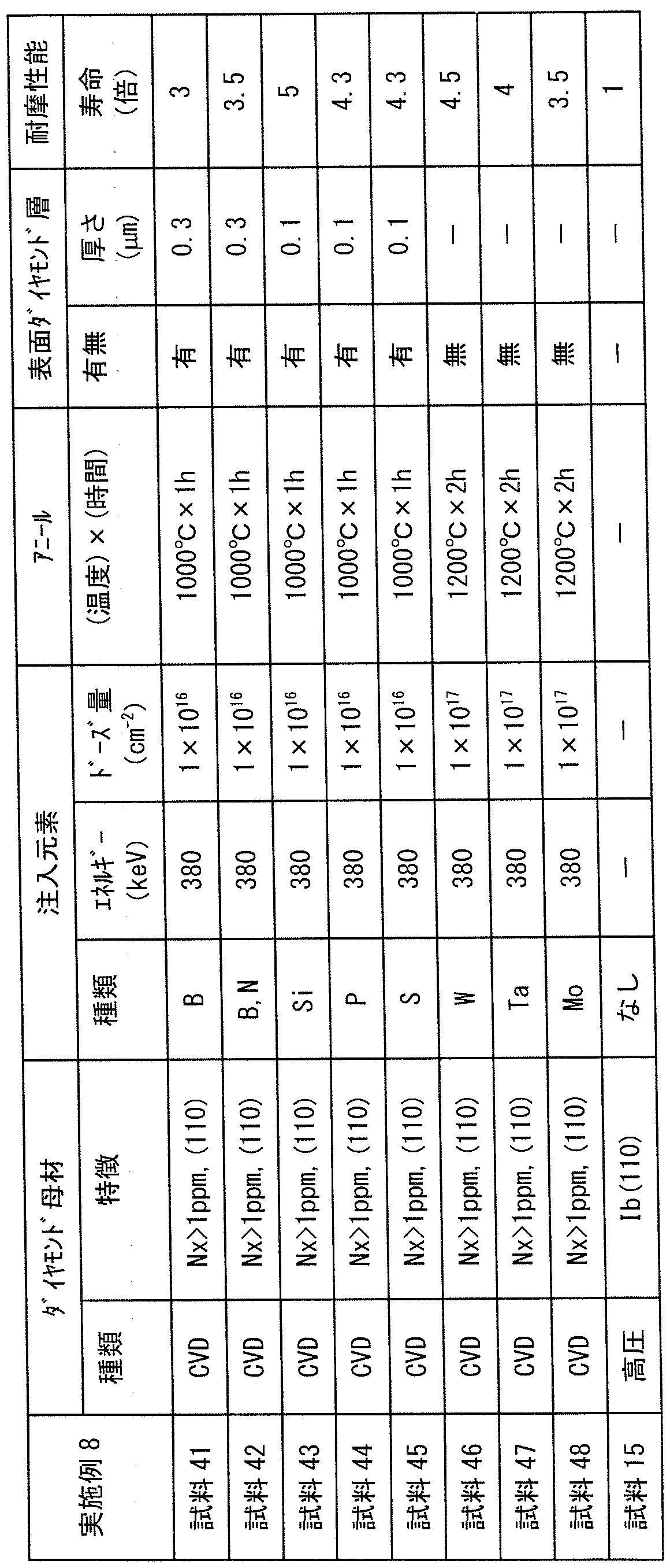
気相合成(具体的にはCVD)の単結晶ダイヤモンド母材を加工し、切削工具用のチップを作製した。切削チップである単結晶ダイヤモンド母材上に、直径0.3μmおよびピッチ0.6μmで正方格子状に配置した穴のあいたマスクを形成し、その穴を通して、イオン注入を行い、安定層を形成した。安定層は水玉模様にダイヤモンド母材に注入された。マスクはイオン注入後に除去された。イオン注入条件は、表4にまとめた通りで、試料51~試料58を作製した。試料51~試料55は、イオン注入後に一般的なターボ分子ポンプの到達圧の真空中で、1000℃で1時間アニールを行った。試料56~試料58は、イオン注入後に一般的なターボ分子ポンプの到達圧の真空中で、1200℃で2時間のアニールを行った。安定層が形成された単結晶ダイヤモンド母材をシャンクに900℃でろう付することによってダイヤモンド切削工具を作製した。こうして得られた本実施例の工具を、鋳鉄を800m/minの速度で切削加工した。鋳鉄との接触部分(逃げ面部分)が1μm摩耗する時点を寿命とすると、本実施例の被覆ダイヤモンド工具は、比較例の試料15のダイヤモンド工具と比べて、寿命が表4にまとめるように長くなり、部分的に形成した安定層形成の効果があることがわかった。試験後の安定層が剥離した部分の面積の総計は、全ての試料で10μm2未満であった。最表面の導電値(抵抗値)を2端子プローブで室温(25℃)で50V印加して評価を行うと、試料51~試料55に関しては、導電値は1μSより高い(抵抗値は1MΩ未満の)値であり、試料56~試料58に関しては、導電値は1mSより高い(抵抗値は1kΩ未満の)値であった。 Example 9
A single crystal diamond base material for vapor phase synthesis (specifically, CVD) was processed to produce a chip for a cutting tool. A mask with holes arranged in a square lattice pattern with a diameter of 0.3 μm and a pitch of 0.6 μm was formed on a single crystal diamond base material as a cutting tip, and ion implantation was performed through the holes to form a stable layer. . The stable layer was injected into the diamond matrix in a polka dot pattern. The mask was removed after ion implantation. The ion implantation conditions are summarized in Table 4, and Sample 51 to Sample 58 were prepared. Samples 51 to 55 were annealed at 1000 ° C. for 1 hour in a vacuum at the ultimate pressure of a general turbo molecular pump after ion implantation. Samples 56 to 58 were annealed at 1200 ° C. for 2 hours in a vacuum at the ultimate pressure of a general turbo molecular pump after ion implantation. A diamond cutting tool was manufactured by brazing a single crystal diamond base material on which a stable layer was formed to a shank at 900 ° C. The tool of this example obtained in this way was cut at a speed of 800 m / min for cast iron. Assuming that the lifetime of the contact portion (flank portion) with the cast iron is 1 μm, the coated diamond tool of this example has a longer lifetime as shown in Table 4 than the diamond tool of Sample 15 of the comparative example. Thus, it was found that there was an effect of forming a partially formed stable layer. The total area of the portions where the stable layer was peeled after the test was less than 10 μm 2 for all the samples. When the evaluation is performed by applying 50 V at the room temperature (25 ° C.) with the conductivity value (resistance value) of the outermost surface for the samples 51 to 55, the conductivity value is higher than 1 μS (the resistance value is less than 1 MΩ). ) Values, and the conductivity values of Sample 56 to Sample 58 were higher than 1 mS (resistance value was less than 1 kΩ).

Claims (16)
- ダイヤモンド母材と、前記ダイヤモンド母材上および前記ダイヤモンド母材の表面から内部の少なくとも一部の少なくともいずれかに配置された少なくとも1層の安定層と、を含む複合ダイヤモンド体。 A composite diamond body comprising a diamond base material and at least one stable layer disposed on at least one of the diamond base material and at least a part of the inside of the diamond base material.
- 前記安定層は、0.001μm以上10μm未満の厚さを有する請求項1に記載の複合ダイヤモンド体。 The composite diamond body according to claim 1, wherein the stable layer has a thickness of 0.001 µm or more and less than 10 µm.
- 前記安定層は、複数の層を含む請求項1または請求項2に記載の複合ダイヤモンド体。 The composite diamond body according to claim 1 or 2, wherein the stable layer includes a plurality of layers.
- 前記安定層は、タングステン、タンタル、モリブデン、ニオブ、バナジウム、クロム、チタン、ジルコニウムおよびハフニウムからなる群から選ばれる少なくとも1種類の金属を含む請求項1から請求項3のいずれか1項に記載の複合ダイヤモンド体。 The said stable layer contains at least 1 sort (s) of metal chosen from the group which consists of tungsten, tantalum, molybdenum, niobium, vanadium, chromium, titanium, zirconium, and hafnium. Composite diamond body.
- 前記安定層は、ルテニウム、オスミウム、ロジウム、イリジウム、パラジウムおよび白金からなる群から選ばれる少なくとも1種類の金属を含む請求項1から請求項3のいずれか1項に記載の複合ダイヤモンド体。 The composite diamond body according to any one of claims 1 to 3, wherein the stable layer includes at least one metal selected from the group consisting of ruthenium, osmium, rhodium, iridium, palladium, and platinum.
- 前記安定層は、炭化タングステン、炭化タンタル、炭化モリブデン、炭化ニオブ、炭化バナジウム、炭化クロム、炭化チタン、炭化ジルコニウム、炭化ハフニウムおよび炭化ケイ素からなる群から選ばれる少なくとも1種類の炭化物を含む請求項1から請求項3のいずれか1項に記載の複合ダイヤモンド体。 2. The stable layer includes at least one carbide selected from the group consisting of tungsten carbide, tantalum carbide, molybdenum carbide, niobium carbide, vanadium carbide, chromium carbide, titanium carbide, zirconium carbide, hafnium carbide, and silicon carbide. The composite diamond body according to any one of claims 3 to 4.
- 前記安定層は、前記ダイヤモンド母材側に位置する内側安定層を含み、
前記内側安定層が、ルテニウム、オスミウム、ロジウム、イリジウム、パラジウムおよび白金からなる群から選ばれる少なくとも1種類の金属を含む請求項1から請求項4および請求項6のいずれか1項に記載の複合ダイヤモンド体。 The stable layer includes an inner stable layer located on the diamond base material side,
7. The composite according to claim 1, wherein the inner stable layer includes at least one metal selected from the group consisting of ruthenium, osmium, rhodium, iridium, palladium, and platinum. Diamond body. - 前記安定層は、前記ダイヤモンド母材側に位置する内側安定層を含み、
前記内側安定層が、炭化タングステン、炭化タンタル、炭化モリブデン、炭化ニオブ、炭化バナジウム、炭化クロム、炭化チタン、炭化ジルコニウム、炭化ハフニウムおよび炭化ケイ素からなる群から選ばれる少なくとも1種類の炭化物を含む請求項1から請求項5のいずれか1項に記載の複合ダイヤモンド体。 The stable layer includes an inner stable layer located on the diamond base material side,
The inner stable layer includes at least one carbide selected from the group consisting of tungsten carbide, tantalum carbide, molybdenum carbide, niobium carbide, vanadium carbide, chromium carbide, titanium carbide, zirconium carbide, hafnium carbide, and silicon carbide. The composite diamond body according to any one of claims 1 to 5. - 前記安定層の少なくとも1層は、前記ダイヤモンド母材上に配置された堆積層である請求項1から請求項8のいずれか1項に記載の複合ダイヤモンド体。 The composite diamond body according to any one of claims 1 to 8, wherein at least one of the stable layers is a deposited layer disposed on the diamond base material.
- 前記安定層の少なくとも1層は、前記ダイヤモンド母材の表面から内部の少なくとも一部に配置されたイオン注入層である請求項1から請求項5のいずれか1項に記載の複合ダイヤモンド体。 The composite diamond body according to any one of claims 1 to 5, wherein at least one of the stable layers is an ion-implanted layer disposed at least partially inside from the surface of the diamond base material.
- 前記イオン注入層は、前記ダイヤモンド母材の表面に垂直な方向から見て、直径が1μmよりも小さな複数の領域に分離している請求項10に記載の複合ダイヤモンド体。 The composite diamond body according to claim 10, wherein the ion-implanted layer is separated into a plurality of regions having a diameter smaller than 1 µm when viewed from a direction perpendicular to the surface of the diamond base material.
- 前記安定層の少なくとも1つの層は、前記ダイヤモンド母材上および前記ダイヤモンド母材の表面から内部の少なくとも一部に配置されたアニール層である請求項1から請求項8のいずれか1項に記載の複合ダイヤモンド体 The at least one layer of the stable layer is an annealing layer disposed on the diamond base material and at least a part of the inside from the surface of the diamond base material. Composite diamond body
- 前記ダイヤモンド母材は、合成単結晶ダイヤモンドおよび合成多結晶ダイヤモンドの少なくとも1種類で形成されている請求項1から請求項12のいずれか1項に記載の複合ダイヤモンド体。 The composite diamond body according to any one of claims 1 to 12, wherein the diamond base material is formed of at least one of a synthetic single crystal diamond and a synthetic polycrystalline diamond.
- 前記ダイヤモンド母材は、非置換型窒素濃度が1ppmより高い気相合成ダイヤモンドで形成されている請求項1から請求項13のいずれか1項に記載の複合ダイヤモンド体。 The composite diamond body according to any one of claims 1 to 13, wherein the diamond base material is formed of vapor-phase synthetic diamond having an unsubstituted nitrogen concentration higher than 1 ppm.
- 前記安定層上に配置された厚さ5μm以下のダイヤモンド表面層をさらに含む請求項1から請求項14のいずれか1項に記載の複合ダイヤモンド体。 The composite diamond body according to any one of claims 1 to 14, further comprising a diamond surface layer having a thickness of 5 µm or less disposed on the stable layer.
- 請求項1から請求項15のいずれか1項に記載の複合ダイヤモンド体を含む複合ダイヤモンド工具。 A composite diamond tool comprising the composite diamond body according to any one of claims 1 to 15.
Priority Applications (5)
| Application Number | Priority Date | Filing Date | Title |
|---|---|---|---|
| EP18201569.3A EP3453476A1 (en) | 2014-10-29 | 2015-10-29 | Composite diamond body and composite diamond tool |
| CN201580059052.9A CN107107206B (en) | 2014-10-29 | 2015-10-29 | Composite diamond body and composite diamond tool |
| EP15855222.4A EP3213842A4 (en) | 2014-10-29 | 2015-10-29 | Composite diamond body and composite diamond tool |
| US15/522,938 US10639725B2 (en) | 2014-10-29 | 2015-10-29 | Composite diamond body and composite diamond tool |
| JP2016556619A JP6706580B2 (en) | 2014-10-29 | 2015-10-29 | Composite diamond body and composite diamond tool |
Applications Claiming Priority (2)
| Application Number | Priority Date | Filing Date | Title |
|---|---|---|---|
| JP2014219991 | 2014-10-29 | ||
| JP2014-219991 | 2014-10-29 |
Publications (1)
| Publication Number | Publication Date |
|---|---|
| WO2016068231A1 true WO2016068231A1 (en) | 2016-05-06 |
Family
ID=55857566
Family Applications (1)
| Application Number | Title | Priority Date | Filing Date |
|---|---|---|---|
| PCT/JP2015/080537 WO2016068231A1 (en) | 2014-10-29 | 2015-10-29 | Composite diamond body and composite diamond tool |
Country Status (5)
| Country | Link |
|---|---|
| US (1) | US10639725B2 (en) |
| EP (2) | EP3213842A4 (en) |
| JP (1) | JP6706580B2 (en) |
| CN (1) | CN107107206B (en) |
| WO (1) | WO2016068231A1 (en) |
Cited By (1)
| Publication number | Priority date | Publication date | Assignee | Title |
|---|---|---|---|---|
| GB2572062B (en) * | 2018-02-09 | 2021-02-24 | Element Six Uk Ltd | Tool cutting element |
Families Citing this family (10)
| Publication number | Priority date | Publication date | Assignee | Title |
|---|---|---|---|---|
| WO2018123042A1 (en) * | 2016-12-28 | 2018-07-05 | 住友電気工業株式会社 | Coating film |
| WO2019035438A1 (en) | 2017-08-15 | 2019-02-21 | 住友電気工業株式会社 | Body obtained by processing solid carbon-containing material, producing method thereof and producing apparatus thereof |
| WO2019035437A1 (en) * | 2017-08-15 | 2019-02-21 | 住友電気工業株式会社 | Body obtained by processing solid carbon-containing material and producing method thereof |
| CN108103472B (en) * | 2017-12-27 | 2020-04-14 | 富耐克超硬材料股份有限公司 | Composite coating cutter and preparation method thereof |
| US11229957B2 (en) * | 2018-10-02 | 2022-01-25 | Jakob Lach Gmbh & Co. Kg | Method for producing a cutting tool for the machining of workpieces and cutting tool |
| CN109231990A (en) * | 2018-11-06 | 2019-01-18 | 河海大学 | A kind of preparation method of tungsten carbide-diamond composite |
| EP4008474A4 (en) * | 2019-08-01 | 2022-11-23 | Sumitomo Electric Hardmetal Corp. | Cutting tool manufacturing method and cutting tool |
| CN110578128B (en) * | 2019-08-26 | 2021-08-20 | 中南钻石有限公司 | Preparation method of dome-shaped polycrystalline diamond compact |
| CN111424248A (en) * | 2020-05-13 | 2020-07-17 | 沈阳理工大学 | Preparation method of high-temperature oxidation-resistant SiC/ZrC coating on surface of carbon/carbon composite material |
| CN115233197B (en) * | 2022-08-09 | 2023-09-15 | 中南钻石有限公司 | Titanium nitride plating diamond and production process thereof |
Citations (4)
| Publication number | Priority date | Publication date | Assignee | Title |
|---|---|---|---|---|
| JP2005324319A (en) * | 2004-04-15 | 2005-11-24 | Kobe Univ | Diamond member and its manufacture method |
| JP2010520067A (en) * | 2007-02-28 | 2010-06-10 | エレメント シックス (プロダクション)(プロプライエタリィ) リミテッド | Machining method of workpiece |
| JP2010527802A (en) * | 2007-05-22 | 2010-08-19 | エレメント シックス リミテッド | Coated diamond |
| JP2013035732A (en) * | 2011-08-10 | 2013-02-21 | Sumitomo Electric Ind Ltd | Single crystal diamond with conduction layer, and tool using the same |
Family Cites Families (24)
| Publication number | Priority date | Publication date | Assignee | Title |
|---|---|---|---|---|
| US3378393A (en) * | 1964-11-19 | 1968-04-16 | Gen Electric | Evaporative application of metal coatings to diamond |
| SE453474B (en) * | 1984-06-27 | 1988-02-08 | Santrade Ltd | COMPOUND BODY COATED WITH LAYERS OF POLYCristalline DIAMANT |
| JPH03232973A (en) * | 1990-02-08 | 1991-10-16 | Daido Steel Co Ltd | Diamond tool |
| US5126207A (en) * | 1990-07-20 | 1992-06-30 | Norton Company | Diamond having multiple coatings and methods for their manufacture |
| US5232469A (en) | 1992-03-25 | 1993-08-03 | General Electric Company | Multi-layer metal coated diamond abrasives with an electrolessly deposited metal layer |
| US5855967A (en) * | 1995-11-29 | 1999-01-05 | Epion Corporation | Method of protecting surfaces on diamond, diamondlike carbon or carbon |
| US5853888A (en) * | 1997-04-25 | 1998-12-29 | The United States Of America As Represented By The Secretary Of The Navy | Surface modification of synthetic diamond for producing adherent thick and thin film metallizations for electronic packaging |
| US6779951B1 (en) * | 2000-02-16 | 2004-08-24 | U.S. Synthetic Corporation | Drill insert using a sandwiched polycrystalline diamond compact and method of making the same |
| WO2001079583A2 (en) * | 2000-04-14 | 2001-10-25 | Technology International, Inc. | Diamonds having improved durability |
| CN100376714C (en) * | 2004-12-08 | 2008-03-26 | 上海江信超硬材料有限公司 | Composite structure of diamond surface coated with glass, aluminium oxide and titanium layers and its manufacturing method |
| EP2400531A3 (en) * | 2005-06-20 | 2012-03-28 | Nippon Telegraph And Telephone Corporation | Diamond semiconductor element and process for producing the same |
| CN100555418C (en) * | 2006-01-24 | 2009-10-28 | 鸿富锦精密工业(深圳)有限公司 | Perpendicular magnetic recording medium and manufacture method thereof |
| US8080312B2 (en) * | 2006-06-22 | 2011-12-20 | Kennametal Inc. | CVD coating scheme including alumina and/or titanium-containing materials and method of making the same |
| EP2108630B1 (en) * | 2007-02-02 | 2016-08-17 | Sumitomo Electric Hardmetal Corp. | Diamond sintered compact |
| WO2008104946A1 (en) * | 2007-02-28 | 2008-09-04 | Element Six (Production) (Pty) Ltd | Tool component |
| JP4982506B2 (en) * | 2009-01-09 | 2012-07-25 | 信越化学工業株式会社 | Method for producing single crystal diamond |
| JP4964268B2 (en) * | 2009-04-10 | 2012-06-27 | 住友電気工業株式会社 | Surface coated cutting tool |
| JP2011079683A (en) * | 2009-10-02 | 2011-04-21 | Shin-Etsu Chemical Co Ltd | Base material for growing single crystal diamond and method for producing single crystal diamond substrate |
| PL2524066T3 (en) * | 2010-01-11 | 2019-02-28 | Iscar Ltd. | Coated cutting tool |
| JP2012086988A (en) * | 2010-10-15 | 2012-05-10 | Sumitomo Electric Ind Ltd | Process for exfoliating diamond |
| US20140341664A1 (en) * | 2012-01-10 | 2014-11-20 | Sumitomo Electric Hardmetal Corp. | Diamond coated tool |
| TWI481752B (en) * | 2012-11-20 | 2015-04-21 | Univ Nat Chiao Tung | Growth method of epitaxial diamond |
| GB2509790B (en) * | 2013-03-27 | 2015-02-25 | Hardide Plc | Superabrasive material with protective adhesive coating and method for producing said coating |
| SG10201505413VA (en) | 2015-01-14 | 2016-08-30 | Iia Technologies Pte Ltd | Electronic device grade single crystal diamonds and method of producing the same |
-
2015
- 2015-10-29 CN CN201580059052.9A patent/CN107107206B/en active Active
- 2015-10-29 JP JP2016556619A patent/JP6706580B2/en active Active
- 2015-10-29 US US15/522,938 patent/US10639725B2/en active Active
- 2015-10-29 EP EP15855222.4A patent/EP3213842A4/en active Pending
- 2015-10-29 WO PCT/JP2015/080537 patent/WO2016068231A1/en active Application Filing
- 2015-10-29 EP EP18201569.3A patent/EP3453476A1/en active Pending
Patent Citations (4)
| Publication number | Priority date | Publication date | Assignee | Title |
|---|---|---|---|---|
| JP2005324319A (en) * | 2004-04-15 | 2005-11-24 | Kobe Univ | Diamond member and its manufacture method |
| JP2010520067A (en) * | 2007-02-28 | 2010-06-10 | エレメント シックス (プロダクション)(プロプライエタリィ) リミテッド | Machining method of workpiece |
| JP2010527802A (en) * | 2007-05-22 | 2010-08-19 | エレメント シックス リミテッド | Coated diamond |
| JP2013035732A (en) * | 2011-08-10 | 2013-02-21 | Sumitomo Electric Ind Ltd | Single crystal diamond with conduction layer, and tool using the same |
Cited By (2)
| Publication number | Priority date | Publication date | Assignee | Title |
|---|---|---|---|---|
| GB2572062B (en) * | 2018-02-09 | 2021-02-24 | Element Six Uk Ltd | Tool cutting element |
| US11407038B2 (en) | 2018-02-09 | 2022-08-09 | Element Six (Uk) Limited | Tool cutting element |
Also Published As
| Publication number | Publication date |
|---|---|
| EP3213842A1 (en) | 2017-09-06 |
| JP6706580B2 (en) | 2020-06-10 |
| CN107107206A (en) | 2017-08-29 |
| CN107107206B (en) | 2020-07-28 |
| US20170320144A1 (en) | 2017-11-09 |
| EP3453476A1 (en) | 2019-03-13 |
| EP3213842A4 (en) | 2018-10-24 |
| JPWO2016068231A1 (en) | 2017-08-10 |
| US10639725B2 (en) | 2020-05-05 |
Similar Documents
| Publication | Publication Date | Title |
|---|---|---|
| JP6706580B2 (en) | Composite diamond body and composite diamond tool | |
| CN101855035B (en) | Member covered with hard coating film and process for the production of the member | |
| EP2305405B1 (en) | Coated member | |
| JP6268530B2 (en) | Surface coated cutting tool with excellent chipping resistance due to hard coating layer | |
| CA2880949C (en) | Coated tool | |
| EP2409798B1 (en) | Surface-coated cutting tool | |
| JP6417959B2 (en) | Surface coated cutting tool with excellent chipping resistance due to hard coating layer | |
| WO2015182746A1 (en) | Surface-coated cutting tool | |
| EP3715026B1 (en) | Coated cutting tool | |
| US20160017499A1 (en) | Coated cutting tool | |
| WO2015174490A1 (en) | Surface coating cutting tool | |
| JP2021100783A (en) | Surface coat cutting tool | |
| JP6709526B2 (en) | Surface coated cutting tool | |
| JP2005138209A (en) | Wear-resistant member | |
| EP3456867B1 (en) | Coated drill | |
| WO2022202729A1 (en) | Coated cutting tool | |
| JP5321360B2 (en) | Surface coated cutting tool | |
| WO2022239139A1 (en) | Cutting tool | |
| WO2023008188A1 (en) | Coated tool and cutting tool | |
| JP5267766B2 (en) | Surface coated cutting tool | |
| JP5321356B2 (en) | Surface coated cutting tool | |
| EP4066970A1 (en) | Coated cutting tool | |
| JP2019171531A (en) | Surface-coated cutting tool excellent in thermal crack resistance and chipping resistance |
Legal Events
| Date | Code | Title | Description |
|---|---|---|---|
| 121 | Ep: the epo has been informed by wipo that ep was designated in this application |
Ref document number: 15855222 Country of ref document: EP Kind code of ref document: A1 |
|
| ENP | Entry into the national phase |
Ref document number: 2016556619 Country of ref document: JP Kind code of ref document: A |
|
| WWE | Wipo information: entry into national phase |
Ref document number: 15522938 Country of ref document: US |
|
| NENP | Non-entry into the national phase |
Ref country code: DE |
|
| REEP | Request for entry into the european phase |
Ref document number: 2015855222 Country of ref document: EP |