WO2016047242A1 - Lighting device - Google Patents
Lighting device Download PDFInfo
- Publication number
- WO2016047242A1 WO2016047242A1 PCT/JP2015/069785 JP2015069785W WO2016047242A1 WO 2016047242 A1 WO2016047242 A1 WO 2016047242A1 JP 2015069785 W JP2015069785 W JP 2015069785W WO 2016047242 A1 WO2016047242 A1 WO 2016047242A1
- Authority
- WO
- WIPO (PCT)
- Prior art keywords
- light source
- led
- led light
- resistor
- lighting device
- Prior art date
Links
- 230000005669 field effect Effects 0.000 claims description 3
- 230000001678 irradiating effect Effects 0.000 claims 1
- 238000004020 luminiscence type Methods 0.000 abstract 2
- 239000000758 substrate Substances 0.000 description 24
- 238000005286 illumination Methods 0.000 description 23
- 238000004088 simulation Methods 0.000 description 11
- 238000000034 method Methods 0.000 description 7
- 230000007423 decrease Effects 0.000 description 6
- 230000006399 behavior Effects 0.000 description 5
- 230000000694 effects Effects 0.000 description 4
- 239000003086 colorant Substances 0.000 description 2
- 230000003247 decreasing effect Effects 0.000 description 2
- OAICVXFJPJFONN-UHFFFAOYSA-N Phosphorus Chemical compound [P] OAICVXFJPJFONN-UHFFFAOYSA-N 0.000 description 1
- 239000003990 capacitor Substances 0.000 description 1
- 238000010586 diagram Methods 0.000 description 1
- 238000005516 engineering process Methods 0.000 description 1
- 238000012986 modification Methods 0.000 description 1
- 230000004048 modification Effects 0.000 description 1
- 230000003287 optical effect Effects 0.000 description 1
Images


Classifications
-
- H—ELECTRICITY
- H05—ELECTRIC TECHNIQUES NOT OTHERWISE PROVIDED FOR
- H05B—ELECTRIC HEATING; ELECTRIC LIGHT SOURCES NOT OTHERWISE PROVIDED FOR; CIRCUIT ARRANGEMENTS FOR ELECTRIC LIGHT SOURCES, IN GENERAL
- H05B45/00—Circuit arrangements for operating light-emitting diodes [LED]
- H05B45/40—Details of LED load circuits
- H05B45/44—Details of LED load circuits with an active control inside an LED matrix
- H05B45/46—Details of LED load circuits with an active control inside an LED matrix having LEDs disposed in parallel lines
-
- F—MECHANICAL ENGINEERING; LIGHTING; HEATING; WEAPONS; BLASTING
- F21—LIGHTING
- F21V—FUNCTIONAL FEATURES OR DETAILS OF LIGHTING DEVICES OR SYSTEMS THEREOF; STRUCTURAL COMBINATIONS OF LIGHTING DEVICES WITH OTHER ARTICLES, NOT OTHERWISE PROVIDED FOR
- F21V19/00—Fastening of light sources or lamp holders
-
- F—MECHANICAL ENGINEERING; LIGHTING; HEATING; WEAPONS; BLASTING
- F21—LIGHTING
- F21V—FUNCTIONAL FEATURES OR DETAILS OF LIGHTING DEVICES OR SYSTEMS THEREOF; STRUCTURAL COMBINATIONS OF LIGHTING DEVICES WITH OTHER ARTICLES, NOT OTHERWISE PROVIDED FOR
- F21V9/00—Elements for modifying spectral properties, polarisation or intensity of the light emitted, e.g. filters
- F21V9/08—Elements for modifying spectral properties, polarisation or intensity of the light emitted, e.g. filters for producing coloured light, e.g. monochromatic; for reducing intensity of light
-
- H—ELECTRICITY
- H01—ELECTRIC ELEMENTS
- H01L—SEMICONDUCTOR DEVICES NOT COVERED BY CLASS H10
- H01L27/00—Devices consisting of a plurality of semiconductor or other solid-state components formed in or on a common substrate
- H01L27/14—Devices consisting of a plurality of semiconductor or other solid-state components formed in or on a common substrate including semiconductor components sensitive to infrared radiation, light, electromagnetic radiation of shorter wavelength or corpuscular radiation and specially adapted either for the conversion of the energy of such radiation into electrical energy or for the control of electrical energy by such radiation
-
- H—ELECTRICITY
- H01—ELECTRIC ELEMENTS
- H01L—SEMICONDUCTOR DEVICES NOT COVERED BY CLASS H10
- H01L33/00—Semiconductor devices with at least one potential-jump barrier or surface barrier specially adapted for light emission; Processes or apparatus specially adapted for the manufacture or treatment thereof or of parts thereof; Details thereof
-
- F—MECHANICAL ENGINEERING; LIGHTING; HEATING; WEAPONS; BLASTING
- F21—LIGHTING
- F21V—FUNCTIONAL FEATURES OR DETAILS OF LIGHTING DEVICES OR SYSTEMS THEREOF; STRUCTURAL COMBINATIONS OF LIGHTING DEVICES WITH OTHER ARTICLES, NOT OTHERWISE PROVIDED FOR
- F21V9/00—Elements for modifying spectral properties, polarisation or intensity of the light emitted, e.g. filters
- F21V9/02—Elements for modifying spectral properties, polarisation or intensity of the light emitted, e.g. filters for simulating daylight
-
- F—MECHANICAL ENGINEERING; LIGHTING; HEATING; WEAPONS; BLASTING
- F21—LIGHTING
- F21Y—INDEXING SCHEME ASSOCIATED WITH SUBCLASSES F21K, F21L, F21S and F21V, RELATING TO THE FORM OR THE KIND OF THE LIGHT SOURCES OR OF THE COLOUR OF THE LIGHT EMITTED
- F21Y2115/00—Light-generating elements of semiconductor light sources
- F21Y2115/10—Light-emitting diodes [LED]
Definitions
- the present invention relates to a lighting device.
- LEDs light-emitting diodes
- an LED package that emits white light is used for an illumination device using LEDs.
- White light emitting LED packages are packaged with LED elements that emit blue light and phosphors that convert blue light into light having a long wavelength (yellow, green, red, etc.). By combining these colors, white light is emitted.
- the method of realizing is general. Even if they are said to be the same white, the color emitted from the LED package differs depending on the amount of blue to be output and the type and amount of phosphor.
- Lighting with a toning function that adjusts the color temperature of illumination light by combining a LED package that emits white light with a high color temperature and an LED package that emits white light with a low color temperature, and controlling the ratio of the amount of light emitted Devices are also widespread.
- LED lighting devices having a dimming function that can adjust the brightness of illumination light by using the characteristics of LEDs whose emission intensity can be easily changed by the amount of current are also widely used.
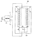
- the LED lighting device 700 shown in FIG. 7 uses an AC power supply 101 as an input power supply and drives LED light sources having two different color temperatures.
- the irradiation unit 720 includes an LED light source 130 including a plurality of LED packages 131 that emit light having a first color temperature, and an LED light source 140 including a plurality of LED packages 141 that emit light having a second color temperature.
- a power supply circuit 110 that generates a DC voltage for driving an LED from an AC power supply can individually drive the LED light source 130 and the LED light source 140 using the anode line 111, the cathode line 112, and the cathode line 113.
- the LED lighting apparatus 700 includes means for controlling some light adjustment and color adjustment, and realizes light adjustment and color adjustment by changing a current for driving the irradiation unit 720.
- FIG. 8 is a graph called a Kruitoff curve, and a region A is a region where a person feels comfortable (so-called “Kreutov comfort zone”). For example, if the brightness is too strong (upper side of the graph) with strong reddish illumination light (low color temperature, left side of the graph) (area B), it tends to feel uncomfortable and uncomfortable.
- FIG. 9 shows an LED lighting device 900 based on this concept.
- a resistor is added to one of the single LEDs connected in parallel.
- Two LED light sources formed by connecting the LEDs in series are connected in parallel, and a resistor R9 is connected to only one of them.
- the illumination unit 920 included in the LED illumination device 900 includes an LED light source 130 including a plurality of LED packages 131 that emit light having a first color temperature, and a second color temperature, similar to the illumination unit 720 included in the LED illumination device 700.
- the LED light source 140 is composed of a plurality of LED packages 141 that emit light of the same number.
- the first color temperature at which the LED package 131 emits light is selected to be lower than the second color temperature at which the LED package 141 emits light.
- the resistor R9 is connected in series with the LED light source 130.
- the irradiation unit 720 includes the cathode line 112 for driving the LED light source 130 and the cathode line 113 for driving the LED light source 140 separately, but the irradiation unit 920 includes only the common cathode line 112. Yes.
- FIG. 10 shows a simulation result calculated from the configuration of the irradiation unit 920.
- the current flowing through the anode line 111 and the cathode line 112 is changed, and the ratio of the current flowing through the LED light source 130, the current flowing through the LED light source 140, and the current flowing through the LED light source 130 is calculated.
- the resistance value of the resistor R9 is adjusted so that the effect can be easily understood.
- the horizontal axis of FIG. 10 indicates the current flowing through the irradiation unit 920, the vertical axis indicates the current flowing through each LED light source, and the ratio of the current flowing through the LED light source 130 to the current flowing through the LED irradiation unit 920.
- the current flowing through the resistor R9 is also small. Since the voltage drop due to the resistor R9 is the product of the resistance value of the resistor R9 and the current value flowing through the resistor R9, this voltage drop is small when the current flowing through the resistor R9 is small. Therefore, the influence of the presence or absence of the resistor R9 is small, and the LED light source 130 and the LED light source 140 pass the same current if they have the same forward voltage. When the current flowing through the irradiation unit 920 is increased from here, the current flowing through the resistor R9 increases accordingly, and the voltage drop due to the resistor R9 increases.
- the voltage applied between the anode line 111 and the cathode line 112 of the LED light source 130 is reduced, and current does not easily flow through the LED light source 130. That is, as the current flowing through the irradiation unit 920 increases, the current flowing from the LED light source 140 decreases from the LED light source 140. Accordingly, the ratio of the current from the LED light source 130 to the current from the irradiation unit 920 is reduced. Since the LED light source 130 has irradiation light with a low color temperature and the LED light source 140 has irradiation light with a high color temperature, as the current flowing through the irradiation unit 920 increases, irradiation with a higher color temperature is obtained as a whole. It is done. With this characteristic, it is possible to keep the emission color within the comfort area of Kruitoff (area A in FIG. 8).
- the LED lighting device 900 can automatically change the color temperature of the emitted color according to the brightness.
- the control of the irradiation unit from the power supply circuit can be simplified to one system instead of two systems at the same time.
- FIG. 11 shows another configuration of the lighting device that automatically changes the color temperature of the emission color according to the brightness.
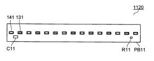
- a difference between the LED illumination device 1100 and the LED illumination device 900 shown in FIG. 11 is that the number of LED packages included in the LED light source 130 and the LED light source 140 is different in the irradiation unit 1120 included in the LED illumination device 1100.
- the LED light source 130 includes seven LED packages 131, and the LED light source 140 includes eight LED packages 141 connected in series. For this reason, the forward voltage of the LED light source 130 is smaller than the forward voltage of the LED light source 140 by one LED package.
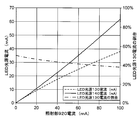
- the simulation result calculated from the structure of the irradiation part 1120 of the LED lighting apparatus 1100 is shown in FIG.
- the notation of this graph is the same as in FIG.
- the resistance value of the resistor R11 connected to the LED light source 130 is adjusted so that the effect can be easily understood.
- the current flowing through the irradiation unit 1120 is small, the voltage drop of the resistor R11 is small, so the influence of the presence or absence of the resistor R11 is small. Therefore, a large amount of current flows through the LED light source 130 having a lower forward voltage than the LED light source 140.
- the current of the irradiation unit 1120 increases, the voltage drop of the resistor R11 increases, so that the current flowing through the LED light source 140 gradually becomes closer to the current flowing through the LED light source 130.
- the current flowing through each of the LED light sources 130 and 140 is equal in that the difference between the voltage drop of the resistor R11 and the forward voltage match. Thereafter, since the voltage drop of the resistor R11 is further increased, the current ratio is reversed, and the LED light source 140 passes more current than the LED power source 130.
- the configuration of the LED lighting device 1100 it is possible to ensure a larger current difference than the LED lighting device 900. That is, the change in color temperature can be increased.
- FIG. 13 shows an LED in which seven LED packages 131 (with hatches in the figure), eight LED packages 141 (without hatches in the figure), resistor R11, and connector C11 are mounted on the printed circuit board PB11. It is a substrate. Since the LED packages 131 and the LED packages 141 are alternately and evenly mounted, color unevenness and luminance unevenness can be minimized. Further, the anode and cathode can be easily connected by simply inserting a harness into the connector C11.
- the LED package 131 and the LED package 141 are staggered. Thereby, surface irradiation is possible with a single substrate, and color unevenness can be suppressed to a minimum by arranging them in a staggered manner.
- the number of LED packages is limited.
- the LED substrate shown in FIGS. 13 and 14 since LED packages of two kinds of light emission colors are evenly arranged as a single unit, color unevenness hardly occurs.
- the larger number of LED packages (LED packages 141) are adjacent to each other at the boundary between adjacent substrates, and thus color unevenness occurs. Arise.
- the LED boards shown in FIG. 14 cannot be arranged vertically and horizontally so that the same color is not adjacent to each other. In this way, there are significant restrictions on the number and arrangement of LED packages.
- the present invention can automatically change the color temperature of a light emission color according to brightness with a simple configuration, and has a high number of light emitting units (for example, LED packages) and a high degree of freedom in arrangement.
- An object is to provide a lighting device.
- a lighting device includes a first light source including at least one first light-emitting portion having a first emission color, and a second light having a second emission color.
- a second light source including at least one light-emitting unit, a resistor connected in series with the first light source, and a switching element connected in series with the second light source, The current flowing through the first light source is converted into a control voltage, and the current flowing through the switching element is controlled by the control voltage (first configuration).
- a field effect transistor is preferably used as the switching element (second configuration).
- the first light source, the second light source, the resistor, and the switching element are mounted on the same printed circuit board (third configuration).
- any one of the first to third configurations it is preferable that a plurality of irradiation units including the first light source, the second light source, the resistor, and the switching element are connected in series or in parallel. (Fourth configuration).
- an illumination device includes a first light source including at least one first light emitting unit having a first emission color, and a second emission color.
- a second light source including at least one second light emitting unit and a resistor connected in series with the first light source, and the first light emitting unit and the second light emitting unit have different numbers.
- the light emitting elements are connected in series.
- the color temperature of the emission color can be automatically changed according to the brightness with a simple configuration, and the number of light emitting units (for example, LED packages) and the degree of freedom in arrangement are high.
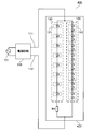
- the LED lighting device 100 is a lighting device that operates using an AC power source 101 as a power source.
- the LED lighting device 100 includes a power supply circuit 110 that generates a DC voltage for driving an LED from an AC power supply 101, and an irradiation unit 120 including the LED.
- the power supply circuit 110 uses the anode line 111 and the cathode line 112 to drive the irradiation unit 120 to emit light. Although not particularly shown, the power supply circuit 110 is provided with some dimming function, and can control a current for driving the irradiation unit 120.
- the irradiation unit 120 includes an LED light source 130 in which a plurality of LED packages (an example of a light emitting unit) 131 having a first emission color are connected in series, and a plurality of LED packages 141 having a second emission color are connected in series.
- the second LED light source 140 thus formed, a switching element Q1 that is an N-channel MOS-FET (field effect transistor), and a resistor R1.
- connection point where the anode sides of the LED light source 130 and the LED light source 140 are connected is connected to the anode line 111.
- the cathode side of the LED light source 130 is connected to one end of the resistor R1.
- the cathode side of the LED light source 140 is connected to the drain of the switching element Q1.
- a node N1 which is a connection point between the LED light source 130 and the resistor R1, is connected to the gate of the switching element Q1.
- a connection point between the other end of the resistor R1 and the source of the switching element Q1 is connected to the cathode line 112.
- the current flowing through the LED light source 130 and the current flowing through the resistor R1 are substantially equal. Further, the current flowing through the LED light source 140 and the current flowing through the switching element Q1 are substantially equal.
- the current flowing through the irradiation unit 120 is the sum of the current flowing through the LED light source 130 and the current flowing through the LED light source 140.
- the current flowing through the irradiation unit 120 is small, the current flowing through the LED light source 130 and the current flowing through the LED light source 140 are both small. Since the current flowing through the resistor R1 is also small, the potential of the node N1 is hardly different from the potential of the cathode line 112. Since the switching element Q1 is an N-channel MOS-FET whose gate is connected to the node N1, almost no current can flow in this state where the voltage between the gate and the source is small. Therefore, almost no current flows through the LED light source 140, and a current flows through the LED light source 130.
- the switching element Q1 passes a current. That is, current flows not only through the LED light source unit 130 but also through the LED light source unit 140.
- the on-resistance of a MOS-FET is very small. Therefore, if the current flowing through the irradiation unit 120 is further increased while the switching element Q1 is turned on, the current flowing through the LED light source unit 140 may increase more than the LED light source unit 130. it can.
- the LED light source 130 when the current flowing through the irradiation unit 120 is small, that is, when the light emission brightness is dark, only the LED light source 130 emits light. However, as the current increases, that is, the LED light source 140 can emit light as the light emission becomes brighter. The ratio of the current flowing through the LED light source 140 gradually increases.
- the LED light source 130 is a white light source with a low color temperature and the LED light source 140 is a white light source with a high color temperature
- the operation emits light at a low color temperature when the brightness is dark and gradually emits light at a higher color temperature when the brightness is bright It becomes.
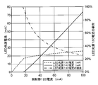
- the simulation result calculated from the structure of the irradiation part 120 of the LED lighting apparatus 100 is shown in FIG.
- the notation of this graph is the same as in FIG.
- the resistance value of the resistor R1 connected to the LED light source 130 is adjusted so that the effect can be easily understood. Until the switching element Q1 is turned on, almost no current flows through the LED light source 140, so that a large difference in current between the LED power source 130 and the LED power source 140 can be secured.
- the number of LED packages included in the LED light source 130 and the LED light source 140, the connection method in series and parallel, and the like are not particularly limited to the examples described above, and are not a plurality but a single LED package. May be.
- the LED lighting device 300 having the configuration shown in FIG. 3 has the same function as the LED lighting device 100 (FIG. 1, the first embodiment).
- the irradiation unit 320 included in the LED lighting device 300 is different in configuration from the irradiation unit 120 included in the LED lighting device 100.
- the irradiation unit 320 includes the LED light source 130 and the LED light source 140 in the same manner as the irradiation unit 120.
- a resistor R3 connected to the anode side in series with the LED light source 130 and a switching element Q3 which is a P-channel MOS-FET connected to the anode side in series with the LED light source 140 are included.
- the operation when the drive current of the irradiation unit 320 is changed is substantially the same as that of the irradiation unit 120. Since the switching element Q3 for controlling the current and the resistor R3 are connected to the anode side, a P-channel type MOS-FET instead of an N-channel type is used as the switching element. Since the switching element Q3 is turned on when the voltage drop due to the resistor R3 becomes larger than a certain level, the behavior is the same as that of the irradiation unit 120.
- the LED lighting device 300 can emit light at a low color temperature when the brightness is dark, and can gradually emit light at a higher color temperature when the brightness is bright, as in the LED lighting device 100.
- the LED light source 140 uses an LED package 142 in which two LED elements are connected in series.
- the LED light source 130 and the LED light source 140 have the same number of LED packages (eight as an example in FIG. 4), but have different forward voltages because the number of LED elements connected in series is different.
- a resistor R4 is connected to the LED light source 130 having a low forward voltage. Since this irradiation unit is equivalent to the LED lighting device 1100 (FIG. 11) except for the number of LEDs in terms of circuit, the ratio of the current flowing through the LED light source 130 according to the drive current flowing through the irradiation unit 420 is the same mechanism.
- the color temperature of the light emission changes. That is, the color temperature can be changed according to the brightness.
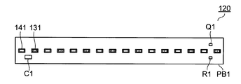
- FIG. 5 is a schematic view of an LED substrate corresponding to the irradiation unit 120 (FIG. 1, the first embodiment).
- the LED substrate shown in FIG. 5 eight LED packages 131, eight LED packages 141, a resistor R1, and a connector C1 are mounted on a printed circuit board PB1. Since the LED packages 131 and the LED packages 141 are alternately and evenly mounted, color unevenness and luminance unevenness can be minimized. Further, the anode and cathode can be easily connected by simply inserting a harness into the connector C1.
- the LED substrate shown in FIG. 6 has the same configuration as that in FIG. 5, but the LED package 131 and the LED package 141 are staggered. Thereby, surface irradiation is possible with a single substrate, and color unevenness can be suppressed to a minimum by arranging them in a staggered manner.
- the LED packages arranged at both ends are different. Therefore, when a plurality of LED substrates are arranged side by side, different LEDs are arranged at the boundary between adjacent substrates, and color unevenness is unlikely to occur. By arranging a plurality of LED substrates in this way, a longer linear light source can be obtained while suppressing the occurrence of color unevenness.
- the LED substrates are arranged vertically to obtain surface irradiation, the LED package 131 and the LED package 141 on the adjacent substrates may be exchanged. In this way, two types of LED packages can be arranged in a staggered manner. Such a configuration is possible because the number of LED packages is the same.
- Such an LED substrate can be realized in the same manner as the irradiation unit 120 in the irradiation unit 320 (FIG. 3, second embodiment) and the irradiation unit 420 (FIG. 4, third embodiment).
- the two types of LED light sources are each formed by connecting LED packages in one row, but the same effect can be obtained even when a plurality of rows are connected in parallel. It is done. By adjusting the number of columns, the overall light emission intensity of each LED light source can be adjusted.
- another resistor may be added to the resistor connected in series with the LED light source and connected in series. According to such a configuration, the change in the ratio of the current flowing through each LED light source after the switching element is turned on can be changed.
- the position at which the switching element or resistor is inserted and the voltage for controlling the switching element can be changed in a path in which each is connected in series. is there.
- the number of LED packages in the LED light source 130 and the LED light source 140 may be different. Further, in the lighting device of the first or second embodiment, an LED package in which different numbers of LED elements are connected in series may be used as in the lighting device of the third embodiment. These can be determined in consideration of the voltage and current required for driving the irradiation unit, the change in the ratio of the current flowing through each LED light source, the arrangement of the LED package, and the like.
- an element other than the N-channel MOS-FET and the P-channel MOS-FET described as an example can be used.
- the same function can be realized with the same circuit configuration as that of the MOS-FET.
- Bipolar transistors and photocouplers can also be used.
- thyristors and triacs can also be used. In these cases, lighting devices having different feelings of use can be realized.
- a circuit configuration using a thyristor as a switching element is an example of a circuit configuration using a thyristor as a switching element.
- a resistor R6 and a capacitor C2 are added to suppress variations in voltage and current.
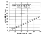
- FIG. 16 is a simulation result showing an example of the behavior of the LED lighting device 500.
- FIG. 16A shows the behavior when the current is increased from the state where the illumination is off.
- the thyristor S1 is turned off. Therefore, no current flows through the LED light source 140, and all the current of the irradiation unit 520 flows through the LED light source 130.
- the current of the resistor R5 also increases, so that the potential of the node N1 increases.
- the node N1 is connected to the gate of the thyristor S1 via the resistor R6, when the potential of the node N1 rises to some extent, the gate current of the thyristor S1 increases and the thyristor S1 is turned on. Since the thyristor S ⁇ b> 1 continues to be turned on until the current is interrupted, in this state, the current flows through both the LED light source 130 and the LED light source 140.
- FIG. 16B shows a simulation result when the current of the irradiation unit 520 is gradually decreased from the state where the thyristor S1 is turned on. Initially, the thyristor S1 is in an ON state, but when the current of the irradiation unit 520 decreases, the currents of the LED light source 130 and the LED light source 140 also decrease. When the current of the LED light source 140, that is, the anode current of the thyristor S1 becomes equal to or lower than the holding current, the thyristor S1 is turned off. Then, all the current of the irradiation unit 520 flows to the LED light source 130.
- the LED lighting device 500 first supplies current only to the LED light source 130 from the off state, and when this current increases to a certain extent, current also flows to the LED light source 140, so the color temperature changes rapidly. To do. Conversely, when the current of the irradiation unit is decreased, the LED light source 140 also flows a current until halfway, so the color temperature does not change much. However, when the current decreases, the current does not flow to the LED light source 140 but only the LED light source 130. Since it is switched to flow, the color temperature changes rapidly. As described above, the lighting device having the characteristic of color temperature having hysteresis with respect to increase / decrease in current can realize a behavior of switching a plurality of color temperatures discretely with a simple circuit configuration.
- the balance of the currents flowing through the LED light source 130 and the LED light source 140 can be adjusted by intentionally significantly differentiating the forward voltages of the LED light source 130 and the LED light source 140. is there.
- the forward voltage of the LED light source 140 is sufficiently lower than the forward voltage of the LED light source 130, only the LED light source 130 is turned on when the thyristor is turned off, and only the LED light source 140 is turned on when the thyristor is turned on.
- the variation of the color temperature rich in variations can be realized by making the structure of the LED light source having the structure according to the present invention a nested structure.
- the structure of the illumination device according to the present invention having different behaviors such as the LED illumination device 500 and the LED illumination device 100. If the LED light source 130 of the LED lighting device 500 is configured like the irradiation unit 120 exemplified in the LED lighting device 100 instead of the LED array having a single color temperature, only the LED light source 130 of the LED lighting device 500 is turned on. Even in a region where the color temperature changes, the color temperature changes depending on the current value.
- the structure of the irradiation part of the present invention and the structure of the irradiation part according to the prior art can be nested and combined.
Abstract
Description
図1~図2を用いて、本発明の第1実施形態に係るLED照明装置について説明する。 <First Embodiment>
The LED lighting device according to the first embodiment of the present invention will be described with reference to FIGS.
色温度の高い白色光源であった場合、明るさが暗いときは低い色温度で発光し、明るくなると次第に高い色温度で発光する動作となる。 To summarize the above description, when the current flowing through the
次に図3を用いて、本発明の第2実施形態に係るLED照明装置について説明する。図3に構成を示すLED照明装置300は、LED照明装置100(図1、第1実施形態)と同様の機能を有する。LED照明装置300の有する照射部320は、LED照明装置100の有する照射部120と構成が異なる。 Second Embodiment
Next, an LED lighting device according to a second embodiment of the present invention will be described with reference to FIG. The
次に図4を用いて、本発明の第3実施形態に係るLED照明装置について説明する。 <Third Embodiment>
Next, an LED lighting apparatus according to a third embodiment of the present invention will be described with reference to FIG.
図5~図6を用いて、本発明に係るLED照明装置が有するLED基板について説明する。 <Fourth embodiment>
The LED substrate included in the LED lighting device according to the present invention will be described with reference to FIGS.
以上、本発明の各実施形態について説明したが、本発明の範囲はこれらに限定されるものではなく、発明の趣旨を逸脱しない範囲で種々の変更を加えて実施することができる。 <Others>
The embodiments of the present invention have been described above, but the scope of the present invention is not limited to these embodiments, and various modifications can be made without departing from the spirit of the invention.
700、900、1100 LED照明装置(従来)
101 交流電源
110 電源回路
111 アノードライン
112、113 カソードライン
120、320、420、520、720、920、1120 照射部
130、140 LED光源
131、141、142 LEDパッケージ
R1、R3、R4、R5、R6、R9、R11 抵抗
Q1、Q3 スイッチング素子
C1、C2、C11 コネクタ
PB1、PB11 プリント基板
S1 サイリスタ 100, 300, 400, 500 LED lighting device (present invention)
700, 900, 1100 LED lighting device (conventional)
101
Claims (5)
- 第1の発光色を有する第1の発光部を少なくとも一つ含む第1の光源と、
第2の発光色を有する第2の発光部を少なくとも一つ含む第2の光源と、
前記第1の光源と直列に接続された抵抗と、
前記第2の光源と直列に接続されたスイッチング素子とを有し、
前記抵抗により前記第1の光源に流れる電流が制御電圧に変換され、
前記制御電圧により前記スイッチング素子に流れる電流が制御されることを特徴とする照明装置。 A first light source including at least one first light emitting unit having a first emission color;
A second light source including at least one second light emitting unit having a second emission color;
A resistor connected in series with the first light source;
A switching element connected in series with the second light source,
A current flowing through the first light source is converted into a control voltage by the resistor,
The lighting device, wherein a current flowing through the switching element is controlled by the control voltage. - 前記スイッチング素子として電界効果トランジスタが使用されることを特徴とする請求項1に記載の照明装置。 The lighting device according to claim 1, wherein a field effect transistor is used as the switching element.
- 前記第1の光源、前記第2の光源、前記抵抗、及び前記スイッチング素子が同一のプリント基板に実装されることを特徴とする請求項1又は請求項2に記載の照明装置。 The lighting device according to claim 1 or 2, wherein the first light source, the second light source, the resistor, and the switching element are mounted on the same printed circuit board.
- 前記第1の光源、前記第2の光源、前記抵抗、及び前記スイッチング素子を含む照射部が直列又は並列に複数接続されることを特徴とする請求項1~請求項3のいずれか1項に記載の照明装置。 The irradiating unit including the first light source, the second light source, the resistor, and the switching element is connected in series or in parallel. The lighting device described.
- 第1の発光色を有する第1の発光部を少なくとも一つ含む第1の光源と、
第2の発光色を有する第2の発光部を少なくとも一つ含む第2の光源と、
前記第1の光源と直列に接続された抵抗とを有し、
前記第1の発光部と前記第2の発光部は、異なる数の発光素子が直列接続されてなることを特徴とする照明装置。 A first light source including at least one first light emitting unit having a first emission color;
A second light source including at least one second light emitting unit having a second emission color;
A resistor connected in series with the first light source;
The first light-emitting unit and the second light-emitting unit include different numbers of light-emitting elements connected in series.
Priority Applications (4)
| Application Number | Priority Date | Filing Date | Title |
|---|---|---|---|
| EP15844974.4A EP3200564A4 (en) | 2014-09-26 | 2015-07-09 | Lighting device |
| CN201580046123.1A CN106797691B (en) | 2014-09-26 | 2015-07-09 | Lighting device |
| US15/513,346 US20170307174A1 (en) | 2014-09-26 | 2015-07-09 | Lighting device |
| JP2016549998A JP6273375B2 (en) | 2014-09-26 | 2015-07-09 | Lighting device |
Applications Claiming Priority (2)
| Application Number | Priority Date | Filing Date | Title |
|---|---|---|---|
| JP2014-196493 | 2014-09-26 | ||
| JP2014196493 | 2014-09-26 |
Publications (1)
| Publication Number | Publication Date |
|---|---|
| WO2016047242A1 true WO2016047242A1 (en) | 2016-03-31 |
Family
ID=55580779
Family Applications (1)
| Application Number | Title | Priority Date | Filing Date |
|---|---|---|---|
| PCT/JP2015/069785 WO2016047242A1 (en) | 2014-09-26 | 2015-07-09 | Lighting device |
Country Status (5)
| Country | Link |
|---|---|
| US (1) | US20170307174A1 (en) |
| EP (1) | EP3200564A4 (en) |
| JP (1) | JP6273375B2 (en) |
| CN (1) | CN106797691B (en) |
| WO (1) | WO2016047242A1 (en) |
Cited By (6)
| Publication number | Priority date | Publication date | Assignee | Title |
|---|---|---|---|---|
| WO2017203989A1 (en) * | 2016-05-26 | 2017-11-30 | シャープ株式会社 | Light emitting device and illumination device |
| JP2018182049A (en) * | 2017-04-12 | 2018-11-15 | Zigenライティングソリューション株式会社 | Light-emitting device and illuminating device |
| JP2018181693A (en) * | 2017-04-18 | 2018-11-15 | パナソニックIpマネジメント株式会社 | Luminaire |
| WO2018233815A1 (en) * | 2017-06-20 | 2018-12-27 | Osram Opto Semiconductors Gmbh | Light arrangement, filament and method for operating a light arrangement |
| JP2020102314A (en) * | 2018-12-20 | 2020-07-02 | 日亜化学工業株式会社 | Light-emitting device and light-emitting circuit |
| US11924937B2 (en) | 2018-10-31 | 2024-03-05 | Nichia Corporation | Light-emitting device, lighting device, and optical member |
Citations (5)
| Publication number | Priority date | Publication date | Assignee | Title |
|---|---|---|---|---|
| JP2004039684A (en) * | 2002-06-28 | 2004-02-05 | Matsushita Electric Works Ltd | Lighting device |
| JP2009009817A (en) * | 2007-06-28 | 2009-01-15 | Toshiba Lighting & Technology Corp | Illumination apparatus |
| CN102595680A (en) * | 2011-01-07 | 2012-07-18 | 英飞特电子(杭州)有限公司 | Multi-output LED (Light-Emitting Diode) constant-current driving circuit |
| WO2013118208A1 (en) * | 2012-02-07 | 2013-08-15 | パナソニック株式会社 | Light-emitting circuit, light-emitting module, and illumination device |
| JP2014157744A (en) * | 2013-02-15 | 2014-08-28 | Panasonic Corp | Light emitting circuit, light emitting module and lighting apparatus |
Family Cites Families (15)
| Publication number | Priority date | Publication date | Assignee | Title |
|---|---|---|---|---|
| CN201045454Y (en) * | 2007-04-24 | 2008-04-09 | 鹤山丽得电子实业有限公司 | LED lamp capable of adjusting colour temperature |
| US7701151B2 (en) * | 2007-10-19 | 2010-04-20 | American Sterilizer Company | Lighting control system having temperature compensation and trim circuits |
| JPWO2011040512A1 (en) * | 2009-10-02 | 2013-02-28 | レシップホールディングス株式会社 | Fluorescent lamp driving device and protective circuit for fluorescent lamp driving device |
| WO2011107138A1 (en) * | 2010-03-01 | 2011-09-09 | Hella Kgaa Hueck & Co. | Method for supplying current to an led array and circuit arrangement for carrying out the method |
| CN102414851B (en) * | 2010-03-11 | 2016-06-22 | 松下知识产权经营株式会社 | The manufacture method of light emitting module, light supply apparatus, liquid crystal indicator and light emitting module |
| JP2012199218A (en) * | 2010-09-09 | 2012-10-18 | Mitsubishi Chemicals Corp | Light-emitting device, lighting system and lighting method |
| US8698388B2 (en) * | 2011-02-03 | 2014-04-15 | Cree, Inc. | Lighting apparatus providing increased luminous flux while maintaining color point and CRI |
| JP2013042099A (en) * | 2011-07-15 | 2013-02-28 | Mitsubishi Chemicals Corp | Circuit board for mounting semiconductor light emitting device, light emitting module, lighting apparatus, and lighting system |
| US9488324B2 (en) * | 2011-09-02 | 2016-11-08 | Soraa, Inc. | Accessories for LED lamp systems |
| US8710754B2 (en) * | 2011-09-12 | 2014-04-29 | Juno Manufacturing Llc | Dimmable LED light fixture having adjustable color temperature |
| CN203457366U (en) * | 2013-07-10 | 2014-02-26 | 艾尔瓦特集成电路科技(天津)有限公司 | LED driver controller and LED driver |
| TWI509835B (en) * | 2013-10-01 | 2015-11-21 | Opto Tech Corp | White led |
| KR102188993B1 (en) * | 2013-11-15 | 2020-12-10 | 삼성디스플레이 주식회사 | Light source unit and back-light assembly having the same |
| CN103957649B (en) * | 2014-05-20 | 2018-03-13 | 贵州光浦森光电有限公司 | LED driving methods and LED illumination circuit |
| CN105792408B (en) * | 2015-01-09 | 2019-02-15 | 松下知识产权经营株式会社 | Lighting system and luminaire |
-
2015
- 2015-07-09 WO PCT/JP2015/069785 patent/WO2016047242A1/en active Application Filing
- 2015-07-09 JP JP2016549998A patent/JP6273375B2/en not_active Expired - Fee Related
- 2015-07-09 EP EP15844974.4A patent/EP3200564A4/en not_active Withdrawn
- 2015-07-09 US US15/513,346 patent/US20170307174A1/en not_active Abandoned
- 2015-07-09 CN CN201580046123.1A patent/CN106797691B/en not_active Expired - Fee Related
Patent Citations (5)
| Publication number | Priority date | Publication date | Assignee | Title |
|---|---|---|---|---|
| JP2004039684A (en) * | 2002-06-28 | 2004-02-05 | Matsushita Electric Works Ltd | Lighting device |
| JP2009009817A (en) * | 2007-06-28 | 2009-01-15 | Toshiba Lighting & Technology Corp | Illumination apparatus |
| CN102595680A (en) * | 2011-01-07 | 2012-07-18 | 英飞特电子(杭州)有限公司 | Multi-output LED (Light-Emitting Diode) constant-current driving circuit |
| WO2013118208A1 (en) * | 2012-02-07 | 2013-08-15 | パナソニック株式会社 | Light-emitting circuit, light-emitting module, and illumination device |
| JP2014157744A (en) * | 2013-02-15 | 2014-08-28 | Panasonic Corp | Light emitting circuit, light emitting module and lighting apparatus |
Cited By (11)
| Publication number | Priority date | Publication date | Assignee | Title |
|---|---|---|---|---|
| WO2017203989A1 (en) * | 2016-05-26 | 2017-11-30 | シャープ株式会社 | Light emitting device and illumination device |
| CN109155344A (en) * | 2016-05-26 | 2019-01-04 | 夏普株式会社 | Light emitting device and lighting device |
| JPWO2017203989A1 (en) * | 2016-05-26 | 2019-01-17 | シャープ株式会社 | Light emitting device and lighting device |
| US10524325B2 (en) | 2016-05-26 | 2019-12-31 | Sharp Kabushiki Kaisha | Light emitting device and illumination device |
| CN109155344B (en) * | 2016-05-26 | 2021-06-01 | 夏普株式会社 | Light emitting device and lighting device |
| JP2018182049A (en) * | 2017-04-12 | 2018-11-15 | Zigenライティングソリューション株式会社 | Light-emitting device and illuminating device |
| JP2018181693A (en) * | 2017-04-18 | 2018-11-15 | パナソニックIpマネジメント株式会社 | Luminaire |
| WO2018233815A1 (en) * | 2017-06-20 | 2018-12-27 | Osram Opto Semiconductors Gmbh | Light arrangement, filament and method for operating a light arrangement |
| US11924937B2 (en) | 2018-10-31 | 2024-03-05 | Nichia Corporation | Light-emitting device, lighting device, and optical member |
| JP2020102314A (en) * | 2018-12-20 | 2020-07-02 | 日亜化学工業株式会社 | Light-emitting device and light-emitting circuit |
| JP7186359B2 (en) | 2018-12-20 | 2022-12-09 | 日亜化学工業株式会社 | Light-emitting device and light-emitting circuit |
Also Published As
| Publication number | Publication date |
|---|---|
| CN106797691B (en) | 2019-07-19 |
| EP3200564A4 (en) | 2018-05-02 |
| CN106797691A (en) | 2017-05-31 |
| EP3200564A1 (en) | 2017-08-02 |
| US20170307174A1 (en) | 2017-10-26 |
| JPWO2016047242A1 (en) | 2017-06-22 |
| JP6273375B2 (en) | 2018-01-31 |
Similar Documents
| Publication | Publication Date | Title |
|---|---|---|
| JP6273375B2 (en) | Lighting device | |
| CN107124786B (en) | LED light source and method for adjusting the hue or color temperature of an LED light source | |
| EP3326434B1 (en) | Lighting apparatus using multiple led strings with current mirror circuitry and methods of operating same | |
| US10182486B2 (en) | LED drive circuit | |
| US7423387B2 (en) | Apparatus and method for controlling colour and colour temperature of light generated by a digitally controlled luminaire | |
| US8847516B2 (en) | Lighting devices including current shunting responsive to LED nodes and related methods | |
| JP5120537B2 (en) | Lighting device | |
| US20080030153A1 (en) | Lighting device | |
| US10136485B1 (en) | Methods for adjusting the light output of illumination systems | |
| US11044793B2 (en) | LED lighting circuit | |
| US10721801B1 (en) | Systems and methods for controlling color temperature and brightness of LED lighting using two wires | |
| JP5454189B2 (en) | Power supply circuit and lighting device | |
| JP5538078B2 (en) | LED power supply | |
| JP2010176984A (en) | Lighting system | |
| JP2009010099A (en) | Lighting system | |
| KR20130025394A (en) | Optoelectronic device | |
| EP3503687B1 (en) | A lighting device and corresponding method for chromatic compensation | |
| JP6090824B2 (en) | LED lighting device | |
| WO2014087874A1 (en) | Illumination device | |
| US20220386431A1 (en) | A light emitting diode, led, based lighting device arranged for emitting a particular emitted light following a planckian locus in a color space | |
| JP5663055B2 (en) | Lighting device and lighting device | |
| JP2008192842A (en) | Lighting system | |
| JP6296051B2 (en) | Lighting device | |
| JP6816354B2 (en) | Lighting device | |
| JP2015008275A (en) | Led module device and led lighting device |
Legal Events
| Date | Code | Title | Description |
|---|---|---|---|
| 121 | Ep: the epo has been informed by wipo that ep was designated in this application |
Ref document number: 15844974 Country of ref document: EP Kind code of ref document: A1 |
|
| ENP | Entry into the national phase |
Ref document number: 2016549998 Country of ref document: JP Kind code of ref document: A |
|
| REEP | Request for entry into the european phase |
Ref document number: 2015844974 Country of ref document: EP |
|
| WWE | Wipo information: entry into national phase |
Ref document number: 2015844974 Country of ref document: EP |
|
| WWE | Wipo information: entry into national phase |
Ref document number: 15513346 Country of ref document: US |
|
| NENP | Non-entry into the national phase |
Ref country code: DE |