WO2016042485A1 - Levelers for copper deposition in microelectronics - Google Patents
Levelers for copper deposition in microelectronics Download PDFInfo
- Publication number
- WO2016042485A1 WO2016042485A1 PCT/IB2015/057097 IB2015057097W WO2016042485A1 WO 2016042485 A1 WO2016042485 A1 WO 2016042485A1 IB 2015057097 W IB2015057097 W IB 2015057097W WO 2016042485 A1 WO2016042485 A1 WO 2016042485A1
- Authority
- WO
- WIPO (PCT)
- Prior art keywords
- set forth
- group
- compound
- composition
- inclusive
- Prior art date
Links
- 0 CCC1[C@@](C2)*(CCC(C)CCCCC(C)C(C)C3(C(C)C)*(C)C3C)C2C1 Chemical compound CCC1[C@@](C2)*(CCC(C)CCCCC(C)C(C)C3(C(C)C)*(C)C3C)C2C1 0.000 description 4
- UAOMVDZJSHZZME-UHFFFAOYSA-N CC(C)NC(C)C Chemical compound CC(C)NC(C)C UAOMVDZJSHZZME-UHFFFAOYSA-N 0.000 description 1
Classifications
-
- C—CHEMISTRY; METALLURGY
- C25—ELECTROLYTIC OR ELECTROPHORETIC PROCESSES; APPARATUS THEREFOR
- C25D—PROCESSES FOR THE ELECTROLYTIC OR ELECTROPHORETIC PRODUCTION OF COATINGS; ELECTROFORMING; APPARATUS THEREFOR
- C25D3/00—Electroplating: Baths therefor
- C25D3/02—Electroplating: Baths therefor from solutions
- C25D3/38—Electroplating: Baths therefor from solutions of copper
-
- C—CHEMISTRY; METALLURGY
- C25—ELECTROLYTIC OR ELECTROPHORETIC PROCESSES; APPARATUS THEREFOR
- C25D—PROCESSES FOR THE ELECTROLYTIC OR ELECTROPHORETIC PRODUCTION OF COATINGS; ELECTROFORMING; APPARATUS THEREFOR
- C25D7/00—Electroplating characterised by the article coated
- C25D7/12—Semiconductors
- C25D7/123—Semiconductors first coated with a seed layer or a conductive layer
-
- H—ELECTRICITY
- H01—ELECTRIC ELEMENTS
- H01L—SEMICONDUCTOR DEVICES NOT COVERED BY CLASS H10
- H01L21/00—Processes or apparatus adapted for the manufacture or treatment of semiconductor or solid state devices or of parts thereof
- H01L21/70—Manufacture or treatment of devices consisting of a plurality of solid state components formed in or on a common substrate or of parts thereof; Manufacture of integrated circuit devices or of parts thereof
- H01L21/71—Manufacture of specific parts of devices defined in group H01L21/70
- H01L21/768—Applying interconnections to be used for carrying current between separate components within a device comprising conductors and dielectrics
- H01L21/76801—Applying interconnections to be used for carrying current between separate components within a device comprising conductors and dielectrics characterised by the formation and the after-treatment of the dielectrics, e.g. smoothing
- H01L21/76802—Applying interconnections to be used for carrying current between separate components within a device comprising conductors and dielectrics characterised by the formation and the after-treatment of the dielectrics, e.g. smoothing by forming openings in dielectrics
- H01L21/76807—Applying interconnections to be used for carrying current between separate components within a device comprising conductors and dielectrics characterised by the formation and the after-treatment of the dielectrics, e.g. smoothing by forming openings in dielectrics for dual damascene structures
-
- H—ELECTRICITY
- H01—ELECTRIC ELEMENTS
- H01L—SEMICONDUCTOR DEVICES NOT COVERED BY CLASS H10
- H01L21/00—Processes or apparatus adapted for the manufacture or treatment of semiconductor or solid state devices or of parts thereof
- H01L21/70—Manufacture or treatment of devices consisting of a plurality of solid state components formed in or on a common substrate or of parts thereof; Manufacture of integrated circuit devices or of parts thereof
- H01L21/71—Manufacture of specific parts of devices defined in group H01L21/70
- H01L21/768—Applying interconnections to be used for carrying current between separate components within a device comprising conductors and dielectrics
- H01L21/76838—Applying interconnections to be used for carrying current between separate components within a device comprising conductors and dielectrics characterised by the formation and the after-treatment of the conductors
- H01L21/76877—Filling of holes, grooves or trenches, e.g. vias, with conductive material
Definitions
- the present invention generally relates to additives for use in an electrolytic deposition chemistry and a method for depositing copper and copper alloys; and more specifically to leveler additives for use in an electrolytic plating solution and a method for copper metallization of interconnect features in semiconductor substrates.
- An interconnect feature is a feature such as a via or trench formed in a dielectric substrate which is then filled with metal, typically copper, to render the interconnect electrically conductive. Copper has been introduced to replace aluminum to form the connection lines and interconnects in semiconductor substrates. Copper, having better conductivity than any metal except silver, is the metal of choice since copper metallization allows for smaller features and uses less energy to pass electricity.
- damascene processing interconnect features of semiconductor IC devices are metallized using electrolytic copper deposition.
- substrates include patterned dielectric films on semiconductor wafer or chip substrates such as, for example, SiO 2 or low- ⁇ dielectric films on silicon or silicon-germanium.
- a wafer has layers of integrated circuitry, e.g., processors, programmable devices, memory devices, and the like, built into one or more layers of dielectric on a semiconductor substrate.
- integrated circuit (IC) devices have been manufactured to contain sub-micron vias and trenches that form electrical connections between layers of interconnect structure (via) and between devices (trench). These features typically have dimensions on the order of about 200 nanometers or less, such as about 150 nanometers, less than about 100 nanometers, or even less than about 50 nanometers.
- a barrier layer such as titanium nitride, tantalum, tantalum nitride, or other layers as are known in the art, is applied to the patterned dielectric prior to the copper metallization that involves copper seed layer deposition (typically by PVD process) followed by electrolytic copper deposition to achieve void-free filling.
- copper seed layer deposition typically by PVD process
- electrolytic copper deposition to achieve void-free filling.
- One conventional semiconductor manufacturing process is the copper damascene system. Specifically, this system begins by etching the circuit architecture into the substrate's dielectric material.
- the architecture is comprised of a combination of the
- a barrier layer is laid over the dielectric to prevent diffusion of the subsequently applied copper layer into the substrate's junctions, followed by physical or chemical vapor deposition of a copper seed layer to provide electrical conductivity for a sequential electrochemical process.
- Copper to fill into the vias and trenches on substrates can be deposited by plating (such as electroless or electrolytic), sputtering, plasma vapor deposition (PVD), and chemical vapor deposition (CVD). It is generally recognized that electrochemical deposition is the best method to apply Cu since it is more economical than other deposition methods and can flawlessly fill into the interconnect features (often called "bottom up" growth or superfilling).
- plating such as electroless or electrolytic
- PVD plasma vapor deposition
- CVD chemical vapor deposition
- electrochemical deposition is the best method to apply Cu since it is more economical than other deposition methods and can flawlessly fill into the interconnect features (often called "bottom up" growth or superfilling).
- excess copper is removed from the facial plane of the dielectric
- Copper plating methods must meet the stringent requirements of the semiconductor industry. For example, copper deposits must be uniform and capable of flawlessly filling the small interconnect features of the device, for example, with openings of 100 nm or smaller.
- Electrolytic copper systems have been developed which rely on so-called “superfilling” or “bottom-up growth” to deposit Cu into various aspect ratio features.
- Superfilling involves filling a feature from the bottom up, rather than at an equal rate on all its surfaces, to avoid seams and pinching off that can result in voiding.
- Multi-part systems consisting of a suppressor and an accelerator as additives have been developed for superfilling, as in Too et al., U.S. Pat. No.6,776,893, which discloses sulfide-based compounds for accelerating and a polyether-based compound for suppressing. Further improvements in bottom up filling are described in Paneccasio US patents 7,303,992 and 7,815,786 which describe suppressors in which a polyether comprising a combination of propylene oxide (PO) and ethylene oxide (EO) is bonded to a nitrogen-containing species.
- PO propylene oxide
- EO ethylene oxide
- the Cu deposit is thicker on the areas of interconnect features than on the field area that does not have features.
- These overgrowth regions are commonly called overplating, overburden, mounding, bumps, or humps. Smaller features generate higher overplating humps due to faster superfill speed. Larger features generally fill slower, which can lead to formation of dimples (also called underplate or underplating), and thus requires additional copper plating to achieve complete planarity. Additional copper plating to correct underplating may further exacerbate overplating.
- Overplating poses challenges for later chemical and mechanical polishing processes that planarize the Cu surface.
- a third organic additive called a“leveler” is typically used to address overgrowth and other issues, as in
- micro-defects may form when electrodepositing Cu for filling interconnect features.
- One defect that can occur is the formation of internal voids inside the features.
- deposition on the side walls and entrance to the feature can pinch off and thereby close access to the depths of the feature especially with features which are small (e.g., ⁇ 100 nm) and/or which have a high aspect ratio (depth:width) if the bottom-up growth rate is not fast enough. Smaller feature size or higher aspect ratio generally requires faster bottom- up speed to avoid pinching off.
- Microvoids are another type of defect which can form during or after electrolytic Cu deposition due to abnormal Cu growth or grain recrystallization that happens after Cu plating, such as, for example, during high temperature anneal steps.
- U.S. Pub. No. 2003/0168343 discloses a method of using an electrolytic deposition chemistry comprising a leveler additive that increases the overall impurity (Cl, S, C, O, N) content of copper metallization in interconnect features.
- Through Silicon Vias are critical components of three-dimensional integrated circuits, and they can be found in RF devices, MEMs, CMOS image sensors, Flash, DRAM, SRAM memories, analog devices, and logic devices.
- TSVs through silicon vias
- the dimensions of through silicon vias are several orders of magnitude larger than the submicron interconnects, but present their own set of problems in gap filling.
- the depth of a TSV depends on the via type (via first or via last), and the application. Via depth can vary from 3 to 500 microns, e.g., from 20 microns to 500 microns, typically between about 30 and about 250 microns, or between about 50 microns and about 250 microns.
- Via openings in TSV have had entry dimensions, such as the diameter, on the order of between about 200 nm to about 200 microns, typically between about 25 microns and about 75 microns.
- compositions appropriate for damascene metallization i.e., the composition comprises the three component superfilling additives including accelerator, suppressor, and leveler
- the composition comprises the three component superfilling additives including accelerator, suppressor, and leveler
- are current density limited such as about 0.10 A/dm 2 . or less to get defect-free fill
- Arana et al. US 2007/0001266 and Lane et al. US 7,081,408 describe various methods for filling through silicon vias.
- Copper plating is also known from, e.g., Eilert (U.S. Pat. No.7,111,149); Rumer et al. (U.S. Pat. No.6,924,551); Shi et al. (U.S. Pub. No.2007/0085198); Ramanathan et al. (U.S. Pub. No.2007/0117348) Heck et al. (U.S. Pub. No.2006/0264029); Williams et al. (U.S. Pub. No.2006/0273455); Rangel (U.S. Pub. No.2006/0278979); and Savastiouk et al. (U.S. Pub. No.2005/0136635). But none of these references, which relate to through silicon via architectures and methods, disclose applicable copper metallization chemistries or plating durations sufficient to fill through silicon via features.
- the additives, compositions and electrolytic plating processes described in Richardson et al. US 2013/0199935 represent a significant advance in the art of filling through silicon vias.
- the TSVs are filled from a plating solution that contains a source of copper ions, chloride ion, and a leveler selected from the group consisting of a quaternized dipyridyl compound and a reaction product of benzyl chloride with
- the present invention is directed to novel levelers, novel electrolytic plating solutions, methods of preparing useful levelers, methods for filling submicron features of integrated circuit devices using plating solutions containing preferred levelers, methods for filling through silicon vias using plating solutions containing preferred levelers, and
- microelectronic devices prepared by processes which comprise filling submicron features of an integrated circuit device, or filling through silicon vias, by electrolytic deposit of copper from plating baths containing the preferred levelers.
- the invention is further directed to novel processes for building copper bumps and pillars in wafer level packaging.
- novel leveler compounds comprise the reaction product of an aliphatic di(t-amine) with a bifunctional alkylating agent corresponding to the formula:
- G is selected from the group consisting of a single covalent bond, -O-, O-((A) r - O) s - and -((A) r -O) s -;
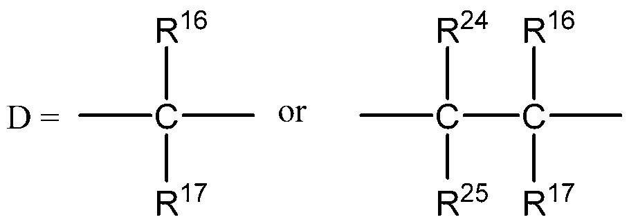
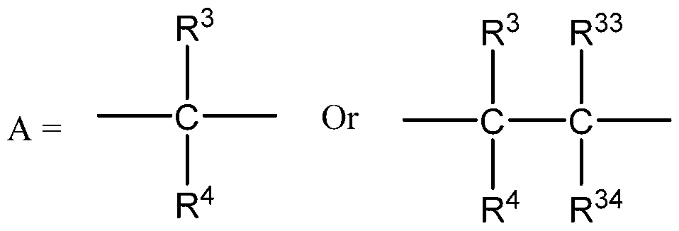
- A has the structure -CR 3 R 4 - or -C(R 3 )(R 4 )C(R 33 )(R 34 )- ; each of p and r is independently an integer between 1 and 6 inclusive, s is an integer between 1 and 10 inclusive, q is an integer between 0 and 6 inclusive; each of R 1 , R 2 , R 3 , R 4 , R 5 , R 6 and R 34 is independently selected from the group consisting of hydrogen and substituted or unsubstituted aliphatic hydrocarbyl comprising 1 to 4 carbon atoms; R 33 is substituted or unsubstituted aliphatic hydrocarbyl having 1 to 4 carbon atoms, Y is a leaving group selected from the group consisting of chloride, bromide, i
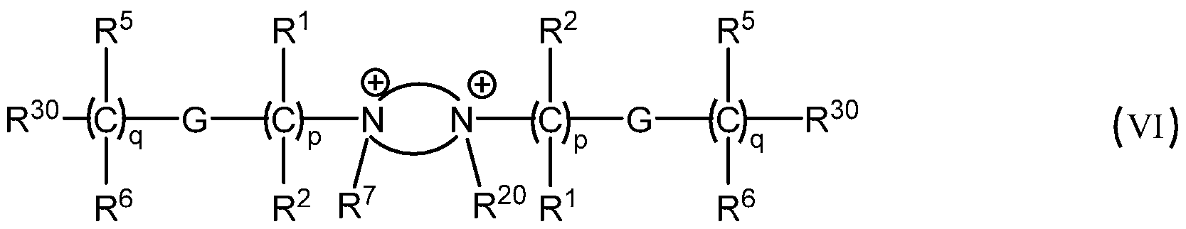
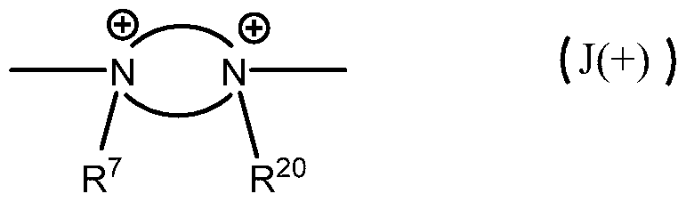
- the leveler compound comprises an oligomer and/or polymer compound selected from the group consisting of salts comprising a cation having the ructure:
- G and A are as defined above; B has the structure;
- each of p, r, t, u, w and y is an integer between 1 and 6 inclusive, each of q, v, x, k, and z is independently an integer between 0 and 6 inclusive, s is an integer between 1 and 10 inclusive, k is at least one when v or x is other than 0, q is at least one when G is other than a single covalent bond; each of R 1 to R 6 , R 9 to R 19 , R 23 , R 25 and R 34 is independently selected from the group consisting of hydrogen or lower alkyl comprising 1 to 4 carbon atoms, each of R 7 , R 8 , R 20 , R 21 , R 22 , R 24 and R 33 is independently selected
- n is between 1 and about 30.
- the leveler compounds comprise compounds
- G, A, B and D are as defined above;
- each of p, r, t, u, w and y is an integer between 1 and 6 inclusive, each of q, v, x, k, and z is independently an integer between 0 and 6 inclusive, s is an integer between 1 and 10 inclusive, k is at least one when v or x is other than 0, q is at least one when G is other than a single covalent bond; each of R 1 to R 6 , R 9 to R 19 , R 23 , R 25 and R 34 is independently selected from the group consisting of hydrogen or lower alkyl comprising 1 to 4 carbon atoms, each of R 7 , R 8 , R 20 , R 21 , R 22 , R 24 and R 33 is independently selected
- R 30 is selected from the group consisting of aliphatic hydrocarbyl, hydroxyl, alkoxy, cyano, carboxyl, alkoxycarbonyl, and amido.
- structure III or VII includes a tertiary amine site, i.e., where x has a value of at least 1, cross-linking may occur at the amine site with another structure III polymer or structure VII compound based on reaction with bifunctional alkylating agent of structure I during synthesis of the leveler.
- Such cross-linked structures are also functional as levelers in the applications described herein.
- the novel levelers are used in processes for electrodeposition of copper on a dielectric or semiconductor base structure.
- a metalizing substrate comprising a conductive layer on the base structure is contacted with an aqueous electrolytic deposition composition; and electrical current is supplied to the electrolytic deposition composition to deposit copper on the substrate.
- the aqueous electrolytic composition comprises copper ions; an acid; a suppressor; and a leveler composition or compound as defined above and/or further defined hereinbelow.
- Novel electrolytic plating compositions and methods have been developed for use in electrolytic deposition of copper in the manufacture of semiconductor integrated circuit devices. More particularly, the novel compositions and methods are effective for filling submicron features of such devices, as well as filling through silicon vias which, e.g., allow electrical interconnection between two or more wafers bonded to each other in a three- dimensional wafer stack. The compositions and processes are also useful for building copper bumps and pillars in wafer level packaging.
- the novel plating compositions contain levelers of two generically different compositions.
- the first class of levelers comprises a predominantly linear configuration that include both ether linkages and quaternized ammonium ions.
- the leveler may be prepared by reaction of a di(t-amine) with an alkylating agent corresponding to the formula:
- G is selected from the group consisting of a covalent single bond, -O-, O-((A) r - O) s - and -((A) r -O) s -, A has the structure
- each of p, q and r is independently an integer between 1 and 6 inclusive, s is an integer between 0 and 10 inclusive, each of R 1 , R 2 , R 3 , R 4 , R 5 , R 6 and R 34 is independently selected from the group consisting of hydrogen and substituted or unsubstituted aliphatic hydrocarbyl comprising 1 to 4 carbon atoms, R 33 is substituted or unsubstituted aliphatic hydrocarbyl having 1 to 4 carbon atoms, Y is a leaving group selected from the group consisting of chloride, bromide, iodide, tosyl, triflate, sulfonate, mesylate, methosulfate, fluorosulfonate, methyl tosylate, and brosylate, Z is selected from the group consisting of R 30 and a leaving group independently selected from the same group as Y, and R 30 is selected from the group consisting of aliphatic hydrocarbyl, hydroxyl, alk
- the leveler compound comprises single reaction species in addition to oligomer and/or polymer.
- Particularly suitable di(t-amine) reactants include: N,N'-dialkyl heterocycles and compounds corresponding to the formula:
- each of t, u, w and y is independently an integer between 1 and 6 inclusive, and each of v, x, z and n is independently an integer between 0 and 6 inclusive
- each of R 7 , R 8 , R 13 , R 20 and R 21 , R 22 , R 24 and R 33 is independently selected from lower alkyl substituents comprising 1 to 4 carbon atoms
- each of each of R 9 to R 12 , R 14 to R 19 , R 23 , R 25 and R 34 is independently selected from the group consisting of hydrogen and substituted or unsubstituted aliphatic hydrocarbyl groups comprising 1 to 4 carbon atoms.
- Alternative di(t-amine) reactants include an N, N'-dialkyl heterocycle corresponding to the formula where R7 and R20 are as defined above.
- Suitable levelers include novel compounds, polymers, and oligomers in the form of quaternary ammonium salts comprising a cation having the structure:
- each of t, u, w, y and, is an integer between 1 and 6 inclusive
- s is an integer between 0 and 10 inclusive
- each of v, x, n and q is independently an integer between 1 and 6 inclusive
- s is an integer between 0 and 10 inclusive
- n is at least one when v or x is other than
- q is t least one when s is other than zero
- each of R 9 to R 12 , R 14 to R 19 , R 23 , R 25 and R 33 is independently selected from the group consisting of hydrogen or lower alkyl comprising 1 to 4 carbon atoms
- each of R 1 , R 2 , R 3 , R 4 , R 5 , R 6 , R 13 , R 22 , R 24 and R 34 is independently selected from the group consisting of hydrogen or lower alkyl comprising 1 to 4 carbon atoms
- the value of s is at least one, or at least two; the value of x is at least one; R13 is alkyl; each of R7, R8, R13, R20, R21, R23, and R33 is methyl; and is the residue of a 5- or 6-membered N, N'-dialkylheterocycle such as, e.g., N,N'- dialkylpiperazine, N,N'-dialkylhexahydropyrimidine, and N,N'-dialkylimidazolidine, more preferably N,N'-dialkylpiperazine, most preferably N,N'-dimethylpiperazine.
- N,N'-dialkylheterocycle such as, e.g., N,N'- dialkylpiperazine, N,N'-dialkylhexahydropyrimidine, and N,N'-dialkylimidazolidine, more preferably N,N'-dialkylpiperazine, most preferably N,N
- Exemplary linear di(t-amine)s include N,N,N',N'-tetramethyl-1,2- diaminoethane, N,N,N',N'-tetramethyl-1,3-diaminopropane, bis(N,N-dimethyl-2-amino)ethyl ether, N,N,N',N'-tetramethyl-1,6-diaminohexane.
- N,N,N’,N’-tetramethyl-1,4-diaminobutane N,N,N’,N’-tetramethyl-1,4-Bis(aminomethyl)cyclohexane
- Exemplary alkylating agents for compounds of formula III include bis(2- chloroethyl) ether, bis(2-chloroethoxy)ethane, 1,6-dichlorohexane, and the analogs of these compounds which contain bromide or other leaving group.
- alkylating agents include bis[2-(2-chloroethoxy)ethyl] ether, 1,3-dichloro-2-propanol, bis(4-chlorobutyl) ether, 1,3-dichloropropan-2-one, 1,2-di(2-chloroethyl)ether, 1,2-dichloroethane, 1,3-dichloropropane, 1,4-dichlorobutane, 1,5-dichloropentane, 1,6-dichlorohexane, 1,7-dichlorobutane, 1,8- dichlorooctane, and anologs of these compounds which contain bromide or other leaving groups.
- Exemplary alkylating agents for the compounds of formula IV include 2-(2- hydroxyethoxy)ethyl chloride, 2-methoxyethyl chloride.1-chloro-4-butanol, hexanol, octanol etc. (3-chloro-2-hydroxypropyl) trimethyl-ammonium chloride, (2- chloroethyl)trimethylammonium chloride, (2-chloroethoxy)benzene, Benzyl chloride, 4- Methylbenzyl chloride, allyl chloride.
- Particularly preferred species of the first class of levelers are oligomers and polymers selected from among compounds having the structural formulas (as in the generic formulae set out above, the brackets indicated that the depicted structures are repeat units of a polymer or oligomer): *
- n is between 1 and 30, e.g., between 2 and 30 or between 5 and 30, or between 5 and 20, and n-x is between 1 and 12, e.g., between 2 and 12, or between 3 and 12, or between 3 and 8.
- compounds having a tertiary amine site e.g., polymers 31 or 32, may cross-link through the amine site with another polymer chain to produce cross-linked polymer structure that may also function as a leveler.
- a diamine is reacted with a difunctional alkylating agent to produce the quaternized structure.
- the diamine and the alkylating agent are dissolved and reacted in a polar organic solvent medium that is compatible with a copper electrolytic plating bath and the conditions under which copper is electrolytically deposited from a copper plating bath in applications such as filling TSVs or wafer level packaging.
- the polar organic solvent medium has an atmospheric boiling point above a temperature at which the quaternization reaction proceeds at a satisfactory rate, e.g., at least 120°, at least 140°C, at least 150°C, or at least 160°C.
- polar solvents such as, e.g., ethylene glycol, diethylene glycol or other similar solvent having a boiling point greater than 180°C.
- Solvents such as dimethylformamide, N- methylpyridine or dimethylsulfoxide are preferably avoided because of possible adverse effect on plating performance where the reaction mixture produced by the leveler synthesis is incorporated into an electrolytic copper plating solution.
- the diamine is preferably present in an initial concentration between about 50 and about 400 g/L, more preferably between about 80 and about 250 g/L.
- the leveler product is polymeric, e.g., where the alkylating agent corresponds to the formula:
- the alkylating agent is preferably present in an initial concentration between about 100 and about 450 g/L, more preferably between about 160 and about 280 g/L, and the molar ratio of alkylating agent to diamine is preferably between about 5:2 and about 1:2, more preferably between about 2:1 and about 1:1.
- the reactant of structure II comprises a tertiary amine site, as in the precursors of compounds 31 and 32, reaction with a bifunctional alkylating agent at the t-amine sites may result in modest cross-linking between the polymer and/or oligomer chains formed in the alkylation reaction.
- the initial concentration of alkylating agent is preferably between about 160 and about 300 g/L, more preferably between about 220 and about 260 g/L, and the molar ratio of alkylating agent to diamine is preferably between about 5:2 and about 1:1.
- the reaction is preferably conducted at a temperature in the range of between about 23°C and about 190°C, more typically between about 120° and about 180°C.
- the leveler reaction mixture is directly diluted in water to produce an aqueous solution that can be combined with accelerator, suppressor, chloride ion, copper salt and acid to yield a novel plating bath of the invention.
- the leveler compound of the first class may be a non-polymeric compound wherein a di(t-amine) is alkylated at both nitrogens with a monofunctional alkylating agent otherwise comparable to that used in synthesis of the polymeric levelers described above.
- These non-polymeric levelers correspond to the structure:
- each of p, r, t, u, w and y is an integer between 1 and 6 inclusive
- each of q, v, x, k, and z is independently an integer between 0 and 6 inclusive
- s is an integer between 1 and 10 inclusive
- k is at least one when v or x is other than
- q is at least one when G is other than a single covalent bond
- each of R 1 to R 6 , R 9 to R 19 , R 23 , R 25 and R 34 is independently selected from the group consisting of hydrogen or lower alkyl comprising 1 to 4 carbon atoms
- each of R 7 , R 8 , R 20 , R 21 , R 22 , R 24 and R 33 is independently selected
- non-polymeric levelers include those corresponding to the formulae:
- a separate class of levelers useful in the novel electrolytic plating methods comprise compounds prepared by the reaction of a dipyridyl or other di(t-amine) compound with a difunctional alkylating agent to produce and intermediate that is reacted with an N,N'- tetraalkylthiourea.
- a dipyridyl or other di(t-amine) compound with a difunctional alkylating agent to produce and intermediate that is reacted with an N,N'- tetraalkylthiourea.
- reactant A corresponds to the structure: Y-(CR 26 R 27 ) i -Ar-(CR 28 R 29 ) j -Z
- each of Y and Z is a leaving group independently selected from among chloride, bromide, iodide, tosyl, triflate, sulfonate, mesylate, methosulfate, fluorosulfonate, methyl tosylate, and brosylate
- Ar is an bivalent aryl residue derived, e.g., from benzene, toluene, xylene, naphthalene, etc.
- each of i and j is an integer between 1 and 12, inclusive
- each of R 26 , R 27 , R 28 , and R 29 is independently selected from among hydrogen and lower alkyl having 1 to 4 carbon atoms.
- Exemplary compounds that can constitute reactant A are p- di(chloromethyl)benzene, 1,4-bis(2-chloroethyl)benzene, m-di(chloromethyl)benzene, and o- di(chloromethyl)benzene.
- A can also be described by structure (I).
- Reactant B is optionally unsubstituted dipyridyl or dipyridyl that is mono- di-, or tri-substituted with any of various ring substituents, including, e.g., alkyl, aryl, aralkyl, hydoxy, alkoxy, aryloxy, cyano, amido, or carboxyl (i.e., hydroxycarbonyl).
- ring substituents including, e.g., alkyl, aryl, aralkyl, hydoxy, alkoxy, aryloxy, cyano, amido, or carboxyl (i.e., hydroxycarbonyl).
- Exemplary compounds that can constitute Reactant B include dipyridyl, ethane, propane, or butane, and any of the di(tert-amine)s described by structure (II).
- Reactant C is preferably a compound that will react with the alkylating agent at the leaving group site, but will not propagate the polymeric reaction.
- Examples include pyridine, thiourea, and N,N,N',N'-tetralkylthiourea
- Alkyl substituents on the urea nitrogen are preferably selected from lower alkyl having 1 to 4 carbon atoms.
- both A and B are dissolved in a solvent medium, e.g., ethylene glycol, and reacted in the solvent medium, preferably at a temperature between about 120°C and about 180°C.
- Reactant A is preferably present in an initial concentration between about 150 and about 200 g/L, more preferably between about 170 and about 180 g/L.
- Reactant B is preferably present in an initial concentration between about 50 and about 200 g/L, more preferably between about 70 and about 100 g/L, and molar ratio of Reactant A to Reactant B is preferably between about 3:1 and about 2:3, more preferably between about 1:1 and about 2:1.
- the reaction generates a salt comprising polymer or oligomer comprising a cation that comprises quaternized dipyridinium repeating units and repeating units comprising the residue of reactant A, and anions derived from the leaving groups Y and Z.
- the intermediate reaction mixture produced by reaction of reactants A and B is cooled to a temperature of preferably less than about 80°C, after which reactant C is added.
- the solution is then heated again between about 120°C and about 180°C to react with the A + B adduct to yield a reaction solution comprising the leveler compound.
- reactant A can initially be reacted with reactant C to produce an adduct which is reacted with reactant B to produce the leveler.
- reactant B can initially be reacted with reactant C to produce an adduct which is reacted with reactant B to produce the leveler.
- reactants A, B and C can all be introduced into the reaction medium and simultaneously reacted to produce a solution comprising the leveler product.
- Weight average molecular weight of the thiourea-based levelers is typically in the range between about 1000 and about 5000. Where reactant C is N,N, N',N'- tetramethylthiourea, the weight average molecular weight may preferably range from about 300 to about 3000.
- a leveler compound produced from p-di(chloromethyl)benzene, dipyridyl and N,N'- tetramethylthiourea has the general structure:
- the novel levelers based on dipyridyl correspond to the above formula except that the substituent on the nitrogens of the thiourea residue may independently be selected from the group consisting of hydrogen and C 1 to C 4 alkyl and the dipyridyl residue and phenylene ring may each bear one or more of the ring substituents listed above.
- leveler compounds of the separate class may correspond to the structure:
- each of R 40 and R 41 is independently selected from the group consisting of hydrogen and C 1 to C 4 alkyl, each of i, j, p, q, R 1 , R 2 , R 5 , R 6 , R 26 , R 27 , R 28 , R 29 , Ar and G is as defined above, and the di(t-amine) residue is derived, e.g., from any of the dipyridyl or other di- (t-amine) compounds listed above.
- the polymeric leveler may typically comprise a mixture of polymers, oligomers and non- polymeric species.
- An electrolytic plating bath for plating semiconductor integrated circuit device preferably comprises copper ions in a concentration between about 0.3 and about 50 g/l, preferably between about 0.5 and about 20 g/l, e.g., in the form of a copper salt such as copper sulfate in a concentration between about 1 and about 40 g/l, an acid, preferably sulfuric acid in a concentration between about 3 and about 150 g/l, preferably between about 5 and about 50 g/l, an accelerator in a concentration between about 15 and about 200 ppm, preferably between about 25 and about 140 ppm, a suppressor in a concentration between about 50 and about 500 ppm, and a novel leveler of the invention in a concentration between about 0.5 and about 30 ppm, preferably between about 1 and about 15 ppm.
- the plating bath also contains chloride ion, e.g., in the form of hydrochloric acid at a concentration between about 30 and about 100 ppm, or between
- a metalizing substrate comprising a seminal conductive layer is initially deposited along the bottom and sidewalls of the vias and trenches, and on those areas of the field to be plated with copper.
- the seminal conductive layer comprises a copper seed layer, or in some cases a conductive polymer such as a polythiophene, polypyrrole or polyaniline, or, in the case of wafer level packaging, an under bump metal pad formed on the semiconductor substrate.
- a copper seed layer may be applied over a dielectric or semiconductor base structure by conventional means such as physical or chemical vapor deposition. In Damascene plating, the base structure is ordinarily a silicon dioxide or other insulating layer formed or bonded on a silicon or other semiconductor chip or wafer. To prevent unwanted diffusion or
- a barrier layer is preferably interposed between the base structure and the metalizing substrate.
- the barrier layer may typically comprise titanium nitride, tantalum, tantalum nitride, tungsten nitride, and other metals and nitrides having comparable properties.
- an electrolytic circuit comprising the electrolytic plating solution, an anode immersed in the plating solution, the metalizing substrate on a dielectric or semiconductor base structure that is formed on or provided by a semiconductor wafer or chip immersed in the electrolytic solution and spaced from the anode, and a DC power source having a positive terminal in electrical communication with the anode and a negative terminal in electrical communication with the metalizing substrate on the wafer or chip which functions as the cathode in the electrolytic circuit.
- DC current is caused to flow through the circuit, causing copper ions from the plating bath to be reduced at the cathodic surface and fill submicron vias and trenches or through silicon vias in the semiconductor substrate.
- the combination of accelerator, suppressor and leveler in the plating bath promotes bottom up filling of the submicron features in the semiconductor substrate.
- Suppressors and levelers both inhibit the plating rate in the field and along the sidewalls of the vias and trenches.
- the accelerators diffuse readily through the bulk electrolytic solution to the bottom of the vias and trenches, and through the boundary layer within the liquid phase at the surface of the metalizing substrate, to function as an electron transfer agent attached to the cathodic copper substrate as the latter grows on the seed layer or other seminal conductive layer.
- Copper ions which are mobile, also diffuse readily through the boundary layer under the influence of the electrolytic field and accept electrons at the cathodic surface to deposit as metallic copper.
- Suppressors and levelers diffuse more slowly, thus resulting in a gradient of progressively decreasing suppressor and leveler concentration vs. depth within the vias and trenches, resulting in an inverse gradient of boundary layer resistance and a corresponding current gradient that promotes more rapid plating at the bottom of the submicron features.
- the levelers are relatively large molecules having a weight average molecular weights typically in the range of 1000 to 5000. Apparently due to a combination of its size and charge density, the leveler typically diffuses more slowly than the suppressor. The slow diffusion rate, coupled with its strong charge, causes the leveler to concentrate at the areas of the metalizing substrate at the surface of an integrated circuit chip or wafer and in the very top reaches of the via. Where it attaches to the substrate, the leveler is not readily displaced by either the accelerator or the suppressor.
- the leveler exhibits a strongly suppressive effect on electrodeposition of copper at the underlying substrate, thus directing the current away from the upper reaches of the via where the leveler concentration is highest to the bottom of the via where the leveler concentration is lowest, and thereby promoting growth of the deposit in the vertical direction faster than growth in the horizontal direction within the via.
- the leveler is concentrated at the exterior surface (the field) of the chip (or other microelectronic device) and the upper reaches of the via, it is effective to retard electrodeposition at on those surfaces, thereby minimizing undesirable overburden and preventing pinching and formation of voids at or near the via entry.
- the novel levelers described herein have been found to possess favorable properties in promoting rapid bottom up filling with minimal formation of voids or overburden
- the electrolytic deposition process operates at a current density between about 1 and about 10 mA/cm 2 and a wafer rotation rate of 10 to 100 rpm.
- Electrolytic solutions which contain the novel leveler can be used in filling submicron features of semiconductor integrated circuit devices, e.g., vias and trenches having a dimension ⁇ 1 ⁇ , more typically ⁇ 100 nm, more preferably between 10 to 30 nm, most typically 20 to 30 nm, in width, and between 60 and 150 nm in depth. Even vias and trenches having a width in the range of 10 to 20 nm may be gap filled using the levelers, plating baths, and plating methods of the invention.
- the submicron features filled using the novel levelers may have aspect ratios >3:1, more typically >4:1, and most typically in the range between about 4:1 and about 10:1.
- the novel aliphatic levelers described herein are especially effective for producing copper deposits of purity, and in particular deposits having relatively minimal content of impurities such as carbon, oxygen, chlorides, sulfur, and nitrogen. This is a signal and advantageous departure from the prior art. While a copper deposit having high impurity can have some advantages such as improving the stress migration resistance of devices, it may not always be advantageous to fill interconnect features in certain devices with copper deposits with high level of impurities. Rather, some devices, particularly memory devices, may require interconnect metallization with a more pure copper deposit. Such a pure copper layer is believed to be less susceptible to microvoiding, have better conductivity and improved resistance to electromigration.
- Plating baths containing the novel levelers further exhibit strong leveling performance for better planarization of the Cu overplate throughout a wafer pattern. Where the substrate presents a dense pattern of especially small interconnect sites, hump height is minimized and mounding is mitigated within a short time frame throughout a wafer pattern.
- TSVs through silicon vias
- TSVs typically have an entry dimension between 1 micrometers and 100 micrometers, a depth dimension between 20 micrometers and 750 micrometers, and an aspect ratio greater than about 2:1, although somewhat lower and significantly higher aspect ratios are also encountered.
- the novel electrolytic plating baths may typically comprise between about 30 and about 80, preferably between about 40 and about 60 g/L copper ion, between about 50 and 120, preferably between about 70 and about 90 g/L acid, preferably sulfuric acid, between about 40 and about 60 ppm chloride ion, between about 2 and about 75, preferably between about 5 and about 50 ppm accelerator, between about 50 and about 300 ppm suppressor and between about 2 and about 50, preferably between about 3 and about 30 ppm leveler.
- Typical aspect ratios range from about 10 to about 25. The process preferably does not use hot entry.
- a seminal conductive layer ordinarily a seed layer is deposited on the wall of the TSV. Current wave form
- the novel electrolytic plating baths may also be used in plating of printed wiring boards, and especially for plating blind vias and the walls of through holes.
- the electrolytic bath preferably comprises between about 15 and about 80 g/L, e.g., between about 30 g/l copper ion, between about 70 and about 225 g/L, e.g., between about 150 and about 225 g/L acid, preferably sulfuric, and between about 50 and about 90 ppm chloride ion.
- Current density is preferably in the range between about 10 and about 40 A/ft 2 .
- the novel levelers are also effective in wafer level packaging applications wherein an electrolytic plating composition containing such a leveler can also be used for building copper bumps and pillars in flip chip packaging or other processes for wafer-level packaging of integrated circuits.
- the electrodeposition process including forming bumps or pillars, forming a redistribution layer, or filling TSVs, the cavity in which copper is to be deposited is first provided with a dielectric liner such as silicon dioxide or silicon nitride.
- the dielectric liner can be provided, e.g., by chemical vapor deposition or plasma vapor deposition. Alternatively, organic dielectrics can be used to mitigate a coefficient of thermal expansion mismatch.
- a photoresist wall of the cavity may have sufficient dielectric properties to obviate the need for a further dielectric layer, but the nature of the vapor deposition process may cause a further dielectric layer to form on the photoresist wall as well.
- a seminal conductive layer is then provided by either chemical vapor deposition of a seed layer or by application of a conductive polymer.
- the seminal conductive layer is deposited only at the bottom of the cavity.
- the bottom can be flat, or comprise a recess filled with polyimide that promotes better bonding.
- This embodiment of the process differs from filling TSVs, in which the seminal conductive layer is formed over the entire surface of the cavity, including bottom and sidewalls, and metalization is carried to deposit copper on both bottom and sidewalls.
- the process can be used to provide the under bump metal pads for flip chip manufacturing in which case the metalizing substrate is limited to the faces of the bonding pads.
- the process can be used to form a copper bump or pillar by bottom-up filling of the cavity formed at its floor by the under bump pad or under bump metal and on its sides by the wall of an opening in a stress buffer layer and/or photoresist that allows access to the pad or under bump metal.
- the aperture size of the cavity is roughly comparable to that of a blind through silicon via, and the parameters of the process for building the bump or pillar are similar to those used for filling blind TSVs.
- the concavity wall provided by openings in photoresist or stress-reducing material is ordinarily not seeded and is therefore non-conductive.
- a semiconductor or dielectric under bump structure at the floor of the cavity is provided with a seminal conductive layer, typically comprising a conductive polymer such as a polyimide.
- the process is not as dependent on balance of accelerator and suppressor as it is in the case of bottom filling submicron vias or TSVs.
- Plating baths useful in wafer level packaging are similar to those used for Damascene processes and filling TSVs.
- sulfuric acid is strongly preferred in the latter applications
- baths containing either sulfuric acid or alkane sulfonic acids such as methane sulfonic acid are highly advantageous for forming copper bumps and pillars.
- the novel compositions and processes are effective for forming bumps and pillars of varying dimensions, with a diameter or width ranging from 20 to 150 ⁇ and a height ranging from 20-210 ⁇ .
- megabumps typically have a diameter or width of 100 to 150 ⁇ and a height of 200 to 210 ⁇
- pillars have a diameter or width of 40 to 60 ⁇ and a height of 40 to 100 ⁇
- microbumps have both a diameter or width and a height in the range of 20 to 30 ⁇ .
- the electrolytic plating bath preferably contains copper sulfate or a copper alkanesulfonate in a concentration between about 25 and about 100 g/L, sulfuric acid or an alkanesulfonic acid in a concentration between about 70 and about 150 g/l, and chloride ion in a concentration of about 30 to about 80 ppm.
- the acid In a plating bath for forming microbumps and pillars, the acid
- the concentration is preferably in the lower end of the aforesaid range, e.g., between about 70 and about 100 g/L, while in forming megabumps the acid concentration is preferably in the higher end of the range, e.g., 120 and about 150 g/L. Also in microbump and pillar applications, the concentration of copper salt is preferably between about 25 and about 60 g/L.
- the electrolytic bath preferably contains an accelerator in a concentration between about 20 and about 60 mg/L, a suppressor in a concentration between about 1000 and about 3000 mg/L and the leveler in a concentration between about 1 and about 60 mg/L.
- Preferred levelers for filling megabumps correspond to the formula: III:
- p+q is in the range of 3 to 5
- G is an ether oxygen -O-.
- R 1 , R 2 , R 5 , R 6 , R 7 , R 8 , R 9 , R 10 , R 18 and R 19 are hydrogen.
- a particularly preferred leveler for such applications is compound 27 as depicted on p.15 wherein R 7 , R 8 , R 20 and R 21 are also hydrogen. Using a bath of such composition a WIF of about 3% can be achieved.
- Bumps and pillars produced using the levelers of structure (III) are generally free of Kirkendall voids, also free of impurities including Cl, S, O and C.
- the plating bath preferably comprises a leveler produced by copolymerization of a di(t-amine) and a di(haloalkyl)aryl compound and terminated by condensation of a haloalkylaryl residue with an N,N'-tetralkylthiourea.
- a leveler produced by copolymerization of a di(t-amine) and a di(haloalkyl)aryl compound and terminated by condensation of a haloalkylaryl residue with an N,N'-tetralkylthiourea.
- each of R 40 and R 41 is independently selected from the group consisting of hydrogen and C 1 to C 4 alkyl
- each of i, j, p, q, R 1 , R 2 , R 5 , R 6 , R 26 , R 27 , R 28 , R 29 , Ar and G is as defined above
- the di(t-amine) residue is derived, e.g., from any of the dipyridyl or other di-(t-amine) compounds listed above.
- An especially preferred leveler for forming microbumps and pillars may be produced from p-di(chloromethyl)benzene, dipyridyl and N,N'- tetramethylthiourea has the structure:
- the novel plating bath and process are effective for producing bumps and pillars having a within feature (WIF) height variation of less than about 10% and a within die (WID) height variation of less than about 10% as well.
- WIF within feature
- WID within die
- Use of the dipyridyl based levelers is effective for achieving high plating speeds while controlling the configuration of bumps and pillars, and in particular for eliminating or controlling the height, depth and configuration of domes and dimples.
- Ethylene Glycol (50 mL) is added to a 3-neck 250mL round bottom flask equipped with stir bar, condenser, and thermometer. Tetramethylthiourea (50mmol), and a,a’- dichloro-p-xylene (50mmol) are added to the reaction flask.
- the solution is stirred at 400rpm and the solution is heated to 170°C and allowed to stir at that temperature for 1 hour.
- the solution is allowed to cool to ⁇ 80°C, at which, 4,4-dipyridyl (25mmol) is added.
- the reaction mixture is then heated back to 170°C and allowed to stir at that temperature for an additional hour.
- the solution is then allowed to cool to room temperature.
- the reaction solution is poured into a 100mL volumetric flask and brought to volume with high purity deionized water.
- An electrodeposition bath was prepared containing CuSO 4 (50 g/L Cu ++ ), sulfuric acid (80 g/L), chloride ion (50 ppm), an accelerator (80 mg/L), an aryl ethoxylate suppressor comprising a combination of propylene oxide and ethylene oxide repeat units (400 mg/L), and a leveler compound produced from copolymerization of p-di(chloromethyl)benzene, dipyridyl and subsequent reaction with N,N'-tetramethylthiourea as described hereinabove (28 mg/L).
- This bath was brought into contact with an array of underbump metal sites in a flip chip die assembly and current was applied at a density effective to deposit copper at a rate between 1 and 8 ⁇ per minute, more typically between 2 and 3.5 ⁇ per minute.
- Plating was performed at a bath temperature in the range of 20-45°C, in particular, at room temperature.
- An array of copper pillars was formed on the underbump metal sites, each pillar having a diameter of approximately 40- 60 ⁇ and a height of approximately 60-80 ⁇ , and having a domed configuration at its distal end.
- the WID for the array of microbumps was ⁇ 10%.
- the height of the dome in each microbump extended no more than4 to 6 ⁇ above a plane defined by the base of the dome within the bump structure, i.e., the WIF was not greater than 10%.
- Microbumps were formed on the underbump sites of a flip chip assembly in the manner described in Example 4 except that the copper salt component of the plating bath was cupric methanesulfonate in a Cu ++ ion concentration of 80 g/L, and the acid component was methanesulfonic acid (80 g/L). Again, each of WID and WIF was not greater than 10%.
- Example 6
- An electrodeposition bath was prepared containing CuSO 4 (50 g/L Cu ++ ), sulfuric acid (80 g/L), chloride ion (50 ppm), an accelerator (3 mg/L), a suppressor comprising a combination of propylene oxide and ethylene oxide repeat units bonded to a nitrogen-containing species (2,500 mg/L), and a leveler compound consisting of compound 27 (15 mg/L).
- This bath was brought into contact with an array of underbump metal sites in a flip chip die assembly and current was applied at density effective to deposit copper at rate of 1 to 8 ⁇ /min. for example, 2 to 3.5 ⁇ /min.
- Plating was performed at a bath temperature in the range of 20-45°C, in particular, at room temperature.
- An array of copper megabumps was formed on the underbump metal sites, each megabump having a diameter of 200 ⁇ and a height of approximately 200 ⁇ , and having a domed configuration at its distal end.
- the WID for the array of megabumps was ⁇ 10%.
- the height of the dome in each megabump extended no more than 20 ⁇ above a plane defined by the base of the dome within the bump structure, i.e., the WIF was not greater than 10%.
Abstract
Description


Claims


Priority Applications (6)
| Application Number | Priority Date | Filing Date | Title |
|---|---|---|---|
| ES15841311T ES2819839T3 (en) | 2014-09-15 | 2015-09-15 | Levelers for copper deposition in microelectronics |
| MYPI2017000380A MY187476A (en) | 2014-09-15 | 2015-09-15 | Levelers for copper deposition in microelectronics |
| KR1020177010057A KR101927687B1 (en) | 2014-09-15 | 2015-09-15 | Levelers for copper deposition in microelectronics |
| JP2017514489A JP6776228B2 (en) | 2014-09-15 | 2015-09-15 | Leveler for copper precipitation in microelectronics |
| CN201580049614.1A CN107079591B (en) | 2014-09-15 | 2015-09-15 | Levelling agents for copper deposition in microelectronics |
| EP15841311.2A EP3195708B1 (en) | 2014-09-15 | 2015-09-15 | Levelers for copper deposition in microelectronics |
Applications Claiming Priority (2)
| Application Number | Priority Date | Filing Date | Title |
|---|---|---|---|
| US201462050574P | 2014-09-15 | 2014-09-15 | |
| US62/050,574 | 2014-09-15 |
Publications (1)
| Publication Number | Publication Date |
|---|---|
| WO2016042485A1 true WO2016042485A1 (en) | 2016-03-24 |
Family
ID=55454197
Family Applications (1)
| Application Number | Title | Priority Date | Filing Date |
|---|---|---|---|
| PCT/IB2015/057097 WO2016042485A1 (en) | 2014-09-15 | 2015-09-15 | Levelers for copper deposition in microelectronics |
Country Status (9)
| Country | Link |
|---|---|
| US (1) | US10294574B2 (en) |
| EP (1) | EP3195708B1 (en) |
| JP (1) | JP6776228B2 (en) |
| KR (1) | KR101927687B1 (en) |
| CN (1) | CN107079591B (en) |
| ES (1) | ES2819839T3 (en) |
| MY (1) | MY187476A (en) |
| TW (1) | TWI710671B (en) |
| WO (1) | WO2016042485A1 (en) |
Cited By (1)
| Publication number | Priority date | Publication date | Assignee | Title |
|---|---|---|---|---|
| JP7422809B2 (en) | 2016-09-22 | 2024-01-26 | マクダーミッド エンソン インコーポレイテッド | Copper deposition in wafer-level packaging of integrated circuits |
Families Citing this family (13)
| Publication number | Priority date | Publication date | Assignee | Title |
|---|---|---|---|---|
| TW200632147A (en) | 2004-11-12 | 2006-09-16 | ||
| WO2018057490A1 (en) * | 2016-09-22 | 2018-03-29 | Macdermid Enthone Inc. | Copper plating method and composition for semiconductor substrates |
| CN109952390A (en) * | 2016-09-22 | 2019-06-28 | 麦克德米德乐思公司 | The electro-deposition of copper in microelectronics part |
| US10483221B2 (en) * | 2017-10-30 | 2019-11-19 | Micron Technology, Inc. | 3DI solder cup |
| EP3508620B1 (en) * | 2018-01-09 | 2021-05-19 | ATOTECH Deutschland GmbH | Ureylene additive, its use and a preparation method therefor |
| US10590541B2 (en) * | 2018-06-15 | 2020-03-17 | Rohm And Haas Electronic Materials Llc | Electroless copper plating compositions and methods for electroless plating copper on substrates |
| CN110938847B (en) * | 2019-10-30 | 2021-11-12 | 苏州清飙科技有限公司 | Copper electroplating leveling agent, preparation method thereof and electroplating solution |
| CN110642731A (en) * | 2019-10-30 | 2020-01-03 | 苏州清飙科技有限公司 | Leveling agent for blind hole full-copper electroplating, preparation method thereof and electroplating solution |
| CN115335434A (en) | 2020-04-03 | 2022-11-11 | 巴斯夫欧洲公司 | Composition for copper bump electrodeposition comprising polyaminoamide type leveling agent |
| KR102339868B1 (en) * | 2021-07-30 | 2021-12-16 | 와이엠티 주식회사 | Leveler and electroplating composition for filling via hole |
| CN113981495B (en) * | 2021-09-30 | 2022-05-27 | 深圳市联合蓝海黄金材料科技股份有限公司 | Cyanide-free gold electroplating solution for wafer electroplating, application of cyanide-free gold electroplating solution and method for wafer gold electroplating |
| WO2023052254A1 (en) | 2021-10-01 | 2023-04-06 | Basf Se | Composition for copper electrodeposition comprising a polyaminoamide type leveling agent |
| WO2024008562A1 (en) | 2022-07-07 | 2024-01-11 | Basf Se | Use of a composition comprising a polyaminoamide type compound for copper nanotwin electrodeposition |
Citations (18)
| Publication number | Priority date | Publication date | Assignee | Title |
|---|---|---|---|---|
| US20030168343A1 (en) | 2002-03-05 | 2003-09-11 | John Commander | Defect reduction in electrodeposited copper for semiconductor applications |
| US6776893B1 (en) | 2000-11-20 | 2004-08-17 | Enthone Inc. | Electroplating chemistry for the CU filling of submicron features of VLSI/ULSI interconnect |
| US20050136635A1 (en) | 2003-12-17 | 2005-06-23 | Sergey Savastiouk | Attachment of integrated circuit structures and other substrates to substrates with vias |
| US6924551B2 (en) | 2003-05-28 | 2005-08-02 | Intel Corporation | Through silicon via, folded flex microelectronic package |
| US20060016693A1 (en) * | 2004-07-22 | 2006-01-26 | Rohm And Haas Electronic Materials Llc | Leveler compounds |
| US7081408B2 (en) | 2004-10-28 | 2006-07-25 | Intel Corporation | Method of creating a tapered via using a receding mask and resulting structure |
| US7111149B2 (en) | 2003-07-07 | 2006-09-19 | Intel Corporation | Method and apparatus for generating a device ID for stacked devices |
| US20060264029A1 (en) | 2005-05-23 | 2006-11-23 | Intel Corporation | Low inductance via structures |
| US20060273455A1 (en) | 2005-06-01 | 2006-12-07 | Intel Corporation | Electronic packaging including die with through silicon via |
| US20060278979A1 (en) | 2005-06-09 | 2006-12-14 | Intel Corporation | Die stacking recessed pad wafer design |
| US20070001266A1 (en) | 2005-06-30 | 2007-01-04 | Leonel Arana | Integrated circuit die containing particle-filled through-silicon metal vias with reduced thermal expansion |
| US20070085198A1 (en) | 2005-10-13 | 2007-04-19 | Wei Shi | Integrated micro-channels for 3D through silicon architectures |
| US20070117348A1 (en) | 2005-11-21 | 2007-05-24 | Shriram Ramanathan | 3D integrated circuits using thick metal for backside connections and offset bumps |
| US7303992B2 (en) | 2004-11-12 | 2007-12-04 | Enthone Inc. | Copper electrodeposition in microelectronics |
| US20130175179A1 (en) * | 2004-03-04 | 2013-07-11 | Coventya, Inc. | Polyamine brightening agent |
| US20130199935A1 (en) | 2008-11-26 | 2013-08-08 | Enthone Inc. | Copper filling of through silicon vias |
| US20130241060A1 (en) * | 2008-11-26 | 2013-09-19 | Enthone Inc. | Method and composition for electrodeposition of copper in microelectronics with dipyridyl-based levelers |
| US8608933B2 (en) | 2002-03-05 | 2013-12-17 | Enthone Inc. | Copper electrodeposition in microelectronics |
Family Cites Families (8)
| Publication number | Priority date | Publication date | Assignee | Title |
|---|---|---|---|---|
| US3770598A (en) | 1972-01-21 | 1973-11-06 | Oxy Metal Finishing Corp | Electrodeposition of copper from acid baths |
| IT1046971B (en) * | 1975-03-11 | 1980-09-10 | Oxy Metal Industries Corp | Baths for electrodeposition of copper - contg soluble prod prepd by reacting alkoxylated polyalkylene-imine with alkylating agent |
| US4036711A (en) * | 1975-12-18 | 1977-07-19 | M & T Chemicals Inc. | Electrodeposition of copper |
| CA1105045A (en) * | 1977-05-04 | 1981-07-14 | Hans G. Creutz (Deceased) | Electrodeposition of copper |
| JP2001073182A (en) * | 1999-07-15 | 2001-03-21 | Boc Group Inc:The | Improved acidic copper electroplating solution |
| CN102105622A (en) * | 2008-06-12 | 2011-06-22 | 古河电气工业株式会社 | Electrolytic copper coating and method of manufacture therefor, and copper electrolyte for manufacturing electrolytic copper coatings |
| TWI500823B (en) * | 2010-03-18 | 2015-09-21 | Basf Se | Composition for metal electroplating comprising leveling agent |
| US20140238868A1 (en) | 2013-02-25 | 2014-08-28 | Dow Global Technologies Llc | Electroplating bath |
-
2015
- 2015-09-14 TW TW104130298A patent/TWI710671B/en active
- 2015-09-15 US US14/854,561 patent/US10294574B2/en active Active
- 2015-09-15 EP EP15841311.2A patent/EP3195708B1/en active Active
- 2015-09-15 JP JP2017514489A patent/JP6776228B2/en active Active
- 2015-09-15 CN CN201580049614.1A patent/CN107079591B/en active Active
- 2015-09-15 WO PCT/IB2015/057097 patent/WO2016042485A1/en active Application Filing
- 2015-09-15 MY MYPI2017000380A patent/MY187476A/en unknown
- 2015-09-15 ES ES15841311T patent/ES2819839T3/en active Active
- 2015-09-15 KR KR1020177010057A patent/KR101927687B1/en active IP Right Grant
Patent Citations (19)
| Publication number | Priority date | Publication date | Assignee | Title |
|---|---|---|---|---|
| US6776893B1 (en) | 2000-11-20 | 2004-08-17 | Enthone Inc. | Electroplating chemistry for the CU filling of submicron features of VLSI/ULSI interconnect |
| US20030168343A1 (en) | 2002-03-05 | 2003-09-11 | John Commander | Defect reduction in electrodeposited copper for semiconductor applications |
| US8608933B2 (en) | 2002-03-05 | 2013-12-17 | Enthone Inc. | Copper electrodeposition in microelectronics |
| US6924551B2 (en) | 2003-05-28 | 2005-08-02 | Intel Corporation | Through silicon via, folded flex microelectronic package |
| US7111149B2 (en) | 2003-07-07 | 2006-09-19 | Intel Corporation | Method and apparatus for generating a device ID for stacked devices |
| US20050136635A1 (en) | 2003-12-17 | 2005-06-23 | Sergey Savastiouk | Attachment of integrated circuit structures and other substrates to substrates with vias |
| US20130175179A1 (en) * | 2004-03-04 | 2013-07-11 | Coventya, Inc. | Polyamine brightening agent |
| US20060016693A1 (en) * | 2004-07-22 | 2006-01-26 | Rohm And Haas Electronic Materials Llc | Leveler compounds |
| US7081408B2 (en) | 2004-10-28 | 2006-07-25 | Intel Corporation | Method of creating a tapered via using a receding mask and resulting structure |
| US7303992B2 (en) | 2004-11-12 | 2007-12-04 | Enthone Inc. | Copper electrodeposition in microelectronics |
| US7815786B2 (en) | 2004-11-12 | 2010-10-19 | Enthone Inc. | Copper electrodeposition in microelectronics |
| US20060264029A1 (en) | 2005-05-23 | 2006-11-23 | Intel Corporation | Low inductance via structures |
| US20060273455A1 (en) | 2005-06-01 | 2006-12-07 | Intel Corporation | Electronic packaging including die with through silicon via |
| US20060278979A1 (en) | 2005-06-09 | 2006-12-14 | Intel Corporation | Die stacking recessed pad wafer design |
| US20070001266A1 (en) | 2005-06-30 | 2007-01-04 | Leonel Arana | Integrated circuit die containing particle-filled through-silicon metal vias with reduced thermal expansion |
| US20070085198A1 (en) | 2005-10-13 | 2007-04-19 | Wei Shi | Integrated micro-channels for 3D through silicon architectures |
| US20070117348A1 (en) | 2005-11-21 | 2007-05-24 | Shriram Ramanathan | 3D integrated circuits using thick metal for backside connections and offset bumps |
| US20130199935A1 (en) | 2008-11-26 | 2013-08-08 | Enthone Inc. | Copper filling of through silicon vias |
| US20130241060A1 (en) * | 2008-11-26 | 2013-09-19 | Enthone Inc. | Method and composition for electrodeposition of copper in microelectronics with dipyridyl-based levelers |
Cited By (1)
| Publication number | Priority date | Publication date | Assignee | Title |
|---|---|---|---|---|
| JP7422809B2 (en) | 2016-09-22 | 2024-01-26 | マクダーミッド エンソン インコーポレイテッド | Copper deposition in wafer-level packaging of integrated circuits |
Also Published As
| Publication number | Publication date |
|---|---|
| CN107079591B (en) | 2020-06-05 |
| EP3195708A1 (en) | 2017-07-26 |
| KR20170054498A (en) | 2017-05-17 |
| JP2017532452A (en) | 2017-11-02 |
| US20160076160A1 (en) | 2016-03-17 |
| TW201623696A (en) | 2016-07-01 |
| EP3195708A4 (en) | 2018-07-18 |
| TWI710671B (en) | 2020-11-21 |
| US10294574B2 (en) | 2019-05-21 |
| EP3195708B1 (en) | 2020-07-01 |
| KR101927687B1 (en) | 2018-12-12 |
| MY187476A (en) | 2021-09-23 |
| CN107079591A (en) | 2017-08-18 |
| ES2819839T3 (en) | 2021-04-19 |
| JP6776228B2 (en) | 2020-10-28 |
Similar Documents
| Publication | Publication Date | Title |
|---|---|---|
| EP3195708B1 (en) | Levelers for copper deposition in microelectronics | |
| US9613858B2 (en) | Method and composition for electrodeposition of copper in microelectronics with dipyridyl-based levelers | |
| US9869029B2 (en) | Composition for metal plating comprising suppressing agent for void free submicron feature filling | |
| EP2199315B1 (en) | Composition for metal electroplating comprising leveling agent | |
| TWI489011B (en) | Composition for metal plating comprising suppressing agent for void free submicron feature filling | |
| JP4888913B2 (en) | Copper electrical deposition method in microelectronics | |
| KR20130092994A (en) | Novel compound and use thereof | |
| WO2011149965A2 (en) | Copper filling of through silicon vias | |
| JP2019510875A (en) | Leveler composition for use in copper deposition in the manufacture of microelectronics | |
| WO2011135673A1 (en) | Novel compound and use thereof | |
| US20180355502A1 (en) | Process for metalization of copper pillars in the manufacture of microelectronics |
Legal Events
| Date | Code | Title | Description |
|---|---|---|---|
| 121 | Ep: the epo has been informed by wipo that ep was designated in this application |
Ref document number: 15841311 Country of ref document: EP Kind code of ref document: A1 |
|
| ENP | Entry into the national phase |
Ref document number: 2017514489 Country of ref document: JP Kind code of ref document: A |
|
| NENP | Non-entry into the national phase |
Ref country code: DE |
|
| REEP | Request for entry into the european phase |
Ref document number: 2015841311 Country of ref document: EP |
|
| WWE | Wipo information: entry into national phase |
Ref document number: 2015841311 Country of ref document: EP |
|
| ENP | Entry into the national phase |
Ref document number: 20177010057 Country of ref document: KR Kind code of ref document: A |