WO2016013984A1 - Process for depositing metal or metalloid chalcogenides - Google Patents
Process for depositing metal or metalloid chalcogenides Download PDFInfo
- Publication number
- WO2016013984A1 WO2016013984A1 PCT/SG2015/050231 SG2015050231W WO2016013984A1 WO 2016013984 A1 WO2016013984 A1 WO 2016013984A1 SG 2015050231 W SG2015050231 W SG 2015050231W WO 2016013984 A1 WO2016013984 A1 WO 2016013984A1
- Authority
- WO
- WIPO (PCT)
- Prior art keywords
- metal
- metalloid
- chalcogen
- substrate
- sputtering
- Prior art date
- Legal status (The legal status is an assumption and is not a legal conclusion. Google has not performed a legal analysis and makes no representation as to the accuracy of the status listed.)
- Ceased
Links
Images
Classifications
-
- C—CHEMISTRY; METALLURGY
- C23—COATING METALLIC MATERIAL; COATING MATERIAL WITH METALLIC MATERIAL; CHEMICAL SURFACE TREATMENT; DIFFUSION TREATMENT OF METALLIC MATERIAL; COATING BY VACUUM EVAPORATION, BY SPUTTERING, BY ION IMPLANTATION OR BY CHEMICAL VAPOUR DEPOSITION, IN GENERAL; INHIBITING CORROSION OF METALLIC MATERIAL OR INCRUSTATION IN GENERAL
- C23C—COATING METALLIC MATERIAL; COATING MATERIAL WITH METALLIC MATERIAL; SURFACE TREATMENT OF METALLIC MATERIAL BY DIFFUSION INTO THE SURFACE, BY CHEMICAL CONVERSION OR SUBSTITUTION; COATING BY VACUUM EVAPORATION, BY SPUTTERING, BY ION IMPLANTATION OR BY CHEMICAL VAPOUR DEPOSITION, IN GENERAL
- C23C14/00—Coating by vacuum evaporation, by sputtering or by ion implantation of the coating forming material
- C23C14/0021—Reactive sputtering or evaporation
- C23C14/0036—Reactive sputtering
- C23C14/0057—Reactive sputtering using reactive gases other than O2, H2O, N2, NH3 or CH4
-
- C—CHEMISTRY; METALLURGY
- C23—COATING METALLIC MATERIAL; COATING MATERIAL WITH METALLIC MATERIAL; CHEMICAL SURFACE TREATMENT; DIFFUSION TREATMENT OF METALLIC MATERIAL; COATING BY VACUUM EVAPORATION, BY SPUTTERING, BY ION IMPLANTATION OR BY CHEMICAL VAPOUR DEPOSITION, IN GENERAL; INHIBITING CORROSION OF METALLIC MATERIAL OR INCRUSTATION IN GENERAL
- C23C—COATING METALLIC MATERIAL; COATING MATERIAL WITH METALLIC MATERIAL; SURFACE TREATMENT OF METALLIC MATERIAL BY DIFFUSION INTO THE SURFACE, BY CHEMICAL CONVERSION OR SUBSTITUTION; COATING BY VACUUM EVAPORATION, BY SPUTTERING, BY ION IMPLANTATION OR BY CHEMICAL VAPOUR DEPOSITION, IN GENERAL
- C23C14/00—Coating by vacuum evaporation, by sputtering or by ion implantation of the coating forming material
- C23C14/06—Coating by vacuum evaporation, by sputtering or by ion implantation of the coating forming material characterised by the coating material
- C23C14/0623—Sulfides, selenides or tellurides
-
- C—CHEMISTRY; METALLURGY
- C23—COATING METALLIC MATERIAL; COATING MATERIAL WITH METALLIC MATERIAL; CHEMICAL SURFACE TREATMENT; DIFFUSION TREATMENT OF METALLIC MATERIAL; COATING BY VACUUM EVAPORATION, BY SPUTTERING, BY ION IMPLANTATION OR BY CHEMICAL VAPOUR DEPOSITION, IN GENERAL; INHIBITING CORROSION OF METALLIC MATERIAL OR INCRUSTATION IN GENERAL
- C23C—COATING METALLIC MATERIAL; COATING MATERIAL WITH METALLIC MATERIAL; SURFACE TREATMENT OF METALLIC MATERIAL BY DIFFUSION INTO THE SURFACE, BY CHEMICAL CONVERSION OR SUBSTITUTION; COATING BY VACUUM EVAPORATION, BY SPUTTERING, BY ION IMPLANTATION OR BY CHEMICAL VAPOUR DEPOSITION, IN GENERAL
- C23C14/00—Coating by vacuum evaporation, by sputtering or by ion implantation of the coating forming material
- C23C14/22—Coating by vacuum evaporation, by sputtering or by ion implantation of the coating forming material characterised by the process of coating
- C23C14/34—Sputtering
- C23C14/35—Sputtering by application of a magnetic field, e.g. magnetron sputtering
-
- H—ELECTRICITY
- H10—SEMICONDUCTOR DEVICES; ELECTRIC SOLID-STATE DEVICES NOT OTHERWISE PROVIDED FOR
- H10P—GENERIC PROCESSES OR APPARATUS FOR THE MANUFACTURE OR TREATMENT OF DEVICES COVERED BY CLASS H10
- H10P14/00—Formation of materials, e.g. in the shape of layers or pillars
- H10P14/20—Formation of materials, e.g. in the shape of layers or pillars of semiconductor materials
- H10P14/22—Formation of materials, e.g. in the shape of layers or pillars of semiconductor materials using physical deposition, e.g. vacuum deposition or sputtering
-
- H—ELECTRICITY
- H10—SEMICONDUCTOR DEVICES; ELECTRIC SOLID-STATE DEVICES NOT OTHERWISE PROVIDED FOR
- H10P—GENERIC PROCESSES OR APPARATUS FOR THE MANUFACTURE OR TREATMENT OF DEVICES COVERED BY CLASS H10
- H10P14/00—Formation of materials, e.g. in the shape of layers or pillars
- H10P14/20—Formation of materials, e.g. in the shape of layers or pillars of semiconductor materials
- H10P14/29—Formation of materials, e.g. in the shape of layers or pillars of semiconductor materials characterised by the substrates
- H10P14/2901—Materials
- H10P14/2921—Materials being crystalline insulating materials
-
- H—ELECTRICITY
- H10—SEMICONDUCTOR DEVICES; ELECTRIC SOLID-STATE DEVICES NOT OTHERWISE PROVIDED FOR
- H10P—GENERIC PROCESSES OR APPARATUS FOR THE MANUFACTURE OR TREATMENT OF DEVICES COVERED BY CLASS H10
- H10P14/00—Formation of materials, e.g. in the shape of layers or pillars
- H10P14/20—Formation of materials, e.g. in the shape of layers or pillars of semiconductor materials
- H10P14/34—Deposited materials, e.g. layers
- H10P14/3402—Deposited materials, e.g. layers characterised by the chemical composition
- H10P14/3436—Deposited materials, e.g. layers characterised by the chemical composition being chalcogenide semiconductor materials not being oxides, e.g. ternary compounds
-
- H—ELECTRICITY
- H10—SEMICONDUCTOR DEVICES; ELECTRIC SOLID-STATE DEVICES NOT OTHERWISE PROVIDED FOR
- H10P—GENERIC PROCESSES OR APPARATUS FOR THE MANUFACTURE OR TREATMENT OF DEVICES COVERED BY CLASS H10
- H10P14/00—Formation of materials, e.g. in the shape of layers or pillars
- H10P14/20—Formation of materials, e.g. in the shape of layers or pillars of semiconductor materials
- H10P14/36—Formation of materials, e.g. in the shape of layers or pillars of semiconductor materials characterised by treatments done before the formation of the materials
-
- H—ELECTRICITY
- H10—SEMICONDUCTOR DEVICES; ELECTRIC SOLID-STATE DEVICES NOT OTHERWISE PROVIDED FOR
- H10P—GENERIC PROCESSES OR APPARATUS FOR THE MANUFACTURE OR TREATMENT OF DEVICES COVERED BY CLASS H10
- H10P14/00—Formation of materials, e.g. in the shape of layers or pillars
- H10P14/20—Formation of materials, e.g. in the shape of layers or pillars of semiconductor materials
- H10P14/29—Formation of materials, e.g. in the shape of layers or pillars of semiconductor materials characterised by the substrates
- H10P14/2901—Materials
Definitions
- the present invention generally relates to a process for making metal or metalloid chalcogenides as nanostructured materials.
- the present invention also relates to the use of the process to create one or multiple 2D monolayers of the metal or metalloid chalcogenide. It also relates to the use of the metal or metalloid chalcogenides in a layered semiconductor device such as a field effect transistor.
- transition-metal dichalcogenides a class of layered semiconductor
- MoS 2 molybdenum disulphide
- monolayer MoS 2 presents a direct band gap (1.8 eV) at the K point of the Brillouin zone, while in few-layer and bulk counterpart an indirect band gap (1.2 eV) is observed.
- MoS 2 could be suitable for applications in effective photovoltaic and photocatalysts under visible light.
- a monolayer MoS 2 transistor has shown a high current on-off ratio of 1 ⁇ 10 9 , high current density and the negligible OFF current using mechanically exfoliated flakes from bulk geological samples. This indicates that the sensitivity of MoS 2 -based field effect transistors (FETs) can be significantly improved which is comparable to silicon-based transistors and better than that from graphene ribbons. In addition, logic circuits and amplifiers have also been demonstrated recently using monolayer MoS 2 .
- the structure of MoS 2 is formed by covalently bonded S-Mo-S two-dimensional (2D) hexagonal atomic trilayer, which weakly bounds with neighboring layers via van der Waals forces.
- a process for making metal or metalloid chalcogenides from a metal or metalloid and an elemental chalcogen using magnetron sputtering is provided.
- the sputtering process may comprise the steps of a) directing sputtering gas ions at a target comprising a metal or metalloid, b) reacting the ejected metal or metalloid atoms from the target surface with an elemental chalcogen vapor and c) assembling the metal or metalloid chalcogenides on a substrate.
- This process may involve a chemical reaction between the ejected metal or metalloid atoms and the chalcogen and may therefore additionally be referred to as a reactive sputtering process.
- the reactive gas comprises an elemental chalcogen vapor.
- the process according to the invention allows producing metal or metalloid chalcogenide films in a controlled way. Films can be grown uniformly over large areas in the form of a few layers of the metal or metalloid chalcogenide.
- the method can be scaled up to large area sample preparation. In this way it is compatible with industry mass production techniques on wafer level.
- the sputtering may be performed in an apparatus comprising: i) a vacuum deposition chamber, ii) a sputtering target comprising the metal or metalloid, iii) a reservoir of elemental chalcogen optionally linked to a vaporizer, iv) a power source to effect ejection of the metal or metalloid and v) a substrate on which the deposition of the metal or metalloid chalcogenide occurs.
- the use of such apparatus allows effectively reacting the elemental chalcogen with the metal or metalloid during the sputtering to form the films.
- the vaporization of the elemental chalcogen can be further controlled by the optional use of a suitable vaporizer. Different crystal structure imperfections may be introduced as compared to known methods.
- the sulphur can be vaporized in a suitable manner using such apparatus when temperatures and partial vapor pressure of the elemental chalcogen are controlled.
- the sputtering gas is provided with a fixed pressure of about 1.0 ⁇ 10 -4 to 3.0 ⁇ 10 -3 mbar.
- the deposition in the sputtering process may be performed with a substrate temperature of between about 300°C and 1000°C.
- a high temperature leads to the deposition of the desired films.
- the chalcogen may be vaporized by heating.
- the vaporized chalcogen may preferably produce a partial pressure of about 1.0 to 9.0 ⁇ 10 -7 mbar.
- a controlled vaporization by heating and a controlled partial pressure of the chalcogen can be utilized for optimal deposition for various applications.
- the process as disclosed above may be performed using a DC power source, with a DC power of less than 10 W for the sputtering.
- the growth rate of the layers can be controlled with high precision by the use of a low power source for sputtering.
- a very low partial argon pressure and a low power source used in the magnetron sputtering process allows to grow materials at a very low rate in a controllable chalcogen vapor environment, which can allow the control of 2D growth down to monolayers with lower defects.
- the process as disclosed herein may comprise the production of a transition metal dichalcogenide.
- the process to create one or multiple 2D monolayers of the transitional chalcogenide on a substrate.
- the 2D monolayers can be produced in high uniformity and precision.
- a metal or metalloid chalcogenide obtainable by the process as disclosed above.
- the chalcogenide can advantageously be grown on various substrates with a defined orientation (e.g. c-axis of MoS 2 perpendicular to the substrate surface) and high quality.
- the metal or metalloid chalcogenide as disclosed above in a layered semiconductor device, such as a field effect transistor.
- the obtained field effect transistors can show an improved performance when being applied in photovoltaic or photocatalyst applications.
- metal or metalloid chalcogenide as disclosed above in nanoelectronics as a catalyst, as a photo-detector, photovoltaic or photocatalyst.
- Transition metal is to be interpreted broadly to include any element in which the filling of the outermost shell to eight electrons within a periodic table is interrupted to bring the penultimate shell from 8 to 18 or 32 electrons.
- Transition elements may include, without limitation, scandium, titanium, vanadium, chromium, manganese, iron, cobalt, nickel, copper, zinc, ytterbium, zirconium, niobium, molybdenum, silver, lanthanum, hafnium, tantalum, tungsten, rhenium, rare-earth elements, cerium, praseodymium, neodymium, promethium, samarium, europium, gadolinium, terbium, dysprosium, holmium, erbium, thulium, yttrium, lutetium, and rhodium.
- post-transition metals which may refer to the metallic elements in the periodic table located between the transition metals (to their left) and the metalloids (to their right). These elements may include gallium, indium and thallium; tin and lead; and bismuth, cadmium and mercury; and aluminium.
- 2D monolayer or ‘2-dimensional monolayer’ is to be interpreted broadly to include substantially flat, two dimensional layers of the chalcogenide on an atomic level.
- Flat thin films (“2D films”) of such layers may have the thickness of one or multiple monolayers of the metal or metalloid chalcogenide. It may typically have a thickness of up to 10 nm.
- inert gas is to be interpreted broadly to include any gas which does not form chemical bonds when used in magnetron sputtering.
- exemplary inert gases include noble gases but may include other gases so long as no chemical bonds are formed.
- chalcogen is to be interpreted broadly to include Group VIA elements.
- Group VIA elements may include sulphur, selenium and tellurium or mixtures thereof.
- film is to be interpreted broadly to include a thin, commonly flexible, form of a material, which may be for example a layer on a surface of a substrate.
- substrate is to be interpreted broadly to include materials upon which one or more layers of the metal or metalloid chalcogenide may be deposited.
- the substrate may comprise any material, as long as it is stable under the conditions applied in the sputtering process.
- target is to be interpreted broadly to include materials from which atoms may be ejected to form a coating on a substrate.
- the ejected atoms from the target may engage in subsequent reactions to form covalent bonds.
- the target may include, but is not limited to, metals or metalloids or materials comprising metals or metalloids or materials comprising transition metals.
- transition metal dichalcogenide is to be interpreted broadly to include materials that comprise transition metals and Group VIA elements. There may be a covalent bond between the transition metal and the atoms of the dichalcogenide.
- magnet sputtering is to be interpreted broadly to include the ejection of atoms from a surface as a consequence of ions impacting that surface and, in some manner, imparting enough energy to some surface atoms to overcome binding energies and cause these atoms to be ejected.
- the term may include ‘reactive sputtering’.
- vapor ‘vaporized’ or ‘vaporizer’ is to be interpreted broadly to include a gaseous phase of the element. As used herein, it refers to the gaseous phase of the chalcogenide, wherein the concentration of the chalcogenide in the atmosphere may be irrelevant.
- the term "about”, in the context of concentrations of components of the formulations, typically means +/- 5% of the stated value, more typically +/- 4% of the stated value, more typically +/- 3% of the stated value, more typically, +/- 2% of the stated value, even more typically +/- 1% of the stated value, and even more typically +/- 0.5% of the stated value.
- range format is merely for convenience and brevity and should not be construed as an inflexible limitation on the scope of the disclosed ranges. Accordingly, the description of a range should be considered to have specifically disclosed all the possible sub-ranges as well as individual numerical values within that range. For example, description of a range such as from 1 to 6 should be considered to have specifically disclosed sub-ranges such as from 1 to 3, from 1 to 4, from 1 to 5, from 2 to 4, from 2 to 6, from 3 to 6 etc., as well as individual numbers within that range, for example, 1, 2, 3, 4, 5, and 6. This applies regardless of the breadth of the range.
- sputtering refers to the ejection of atoms from the surface of a target as a consequence of ions impacting that surface and, in some manner, imparting enough energy to some surface atoms to overcome binding energies and cause these atoms to be ejected. Sputtering is most commonly used as a method of depositing coatings onto other surfaces.
- the sputtering according to the invention preferably provides for a target subjected to ion bombardment (“ion-beam sputtering”). Additionally, the atoms ejected from the target may engage in chemical reactions (“reactive sputtering”) with a reactive gas of the elemental chalcogen present in the process (preferably a vaporized chalcogen) and thus the deposited coating will have a different chemical composition from the target.
- the items to be coated generally referred to as the substrates, are preferably placed in locations (with respect to the ion bombarded surface) in which their surfaces will intercept the greatest flux of ejected atoms, and thus be coated.
- magnetron sputtering magnetic fields are employed to help confine electrons which generate the plasma which is the source of bombarding ions. This confinement greatly increases both the sputtering rate and the system efficiency by minimizing the loss of both ions and ionizing electrons.
- the process may be applicable to large scale production of the metal or metalloid chalcogenides. It may be applicable to conventional present semiconductor fabrication processes. It may be applicable for the fabrication of 8 inch wafers.
- the process as disclosed above may comprise the steps of a) directing sputtering gas ions at a target comprising a metal or metalloid (ion-beam sputtering), b) reacting the ejected metal or metalloid atoms from the target surface with an elemental chalcogen vapor (reactive sputtering) and c) assembling the metal or metalloid chalcogenides on a substrate.
- Sputtering may be conducted in a vacuum deposition chamber and in the presence of an inert sputtering gas, such as argon, that may be maintained under very low pressure.
- the inert sputtering gas may form a plasma, which may contain a reactive gas, for example elemental chalcogen, optionally linked to a vaporizer.
- the material to be sputtered (referred to as the target) may be connected to the negative terminal of a DC power supply and may serve as a cathode.
- the target is preferably a metal or metalloid.
- the sputtering process may be performed in an apparatus comprising: i) a vacuum deposition chamber, ii) a sputtering target comprising the metal or metalloid, iii) a reservoir of elemental chalcogen optionally linked to a vaporizer, iv) a power source to effect the ejection of metal or metalloid atoms and v) a substrate on which the deposition of the metal or metalloid chalcogenide occurs.
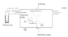
- Figure 1 Illustrative in this context is Figure 1, in which an exemplary apparatus is shown. It consists of a chamber, which is connected to a pump for production of a vacuum. Introduced into this chamber is a sputtering target, from which atoms can be ejected.
- a substrate On the opposite side and in a straight line of the sputtering target is a substrate, on which the deposition of the metal or metalloid chalcogenide may occur.
- a reservoir containing the elemental chalcogen, provided as a powder according to a preferred embodiment, which is wrapped in heating tape. This effects small amounts of the chalcogen to evaporate and, through a leaking valve, reach the vacuum chamber in a vaporized state.
- the sputtering gas in the example shown as Argon, may be ionized and thereby ejecting atoms from the sputtering target.
- the ejected atoms originating from the sputtering may react with the chalcogen and the reaction product may self-assemble on the substrate, thereby forming a thin film, optionally a monolayer.
- the process can be used to create such monolayer, but also two layers, three layers, four layers, five layers, six layers, seven layers or multiple layers of small number, but controlled number on the substrate by altering the power of the ion beam or the deposition time.
- the process as disclosed above may be performed with a substrate temperature of between about 300 °C and about 1000°C, or between about 300 °C and about 900 °C, or between about 300 °C and about 800 °C, or between about 300 °C and about 700 °C, or between about 300 °C and about 600 °C, or between about 300 °C and about 500 °C, or between about 300 °C and about 400 °C, or between about 400 °C and about 1000 °C, or between about 500 °C and about 1000 °C, or between about 600 °C and about 1000 °C, or between about 700 °C and about 1000 °C, or between about 800 °C and about 1000 °C, or between about 900 °C and about 1000 °C, or between about 400 °C and about 900 °C, or between about 500 °C and about 800 °C, or between about 600 °C and about 800 °C, or preferably between about 650 °C and about
- the chalcogen may be vaporized by heating.
- the heating may be effected using a variety of heat sources, which may include, but are not limited to, heating tape, oil bath, sand bath, oven or water bath.
- the heating of the chalcogen is performed by using wrapped heating tape.
- the heating process may result in the vaporized chalcogen producing a partial pressure in the vacuum chamber during the sputtering.
- the vaporized chalcogen produces a partial pressure of about 1.0 to about 9.0 ⁇ 10 -7 mbar, or about 2.0 to about 9.0 ⁇ 10 -7 mbar, or about 3.0 to about 9.0 ⁇ 10 -7 mbar, or about 4.0 to about 9.0 ⁇ 10 -7 mbar, or about 5.0 to about 9.0 ⁇ 10 -7 mbar, or about 6.0 to about 9.0 ⁇ 10 -7 mbar, or about 7.0 to about 9.0 ⁇ 10 -7 mbar, or about 8.0 to about 9.0 ⁇ 10 -7 mbar, or about 1.0 to about 8.0 ⁇ 10 -7 mbar, or about 1.0 to about 7.0 ⁇ 10 -7 mbar, or about 1.0 to about 6.0 ⁇ 10 -7 mbar, or about 1.0 to about 5.0 ⁇ 10 -7 mbar, or about 1.0 to about 4.0 ⁇ 10 -7 mbar, or about 1.0 to about 3.0 ⁇ 10 -7 mbar
- a range of about 3.0 to about 5.0 ⁇ 10 -7 mbar can be particularly mentioned. It can be critical for optimal performance to control this partial gas pressure carefully using for instance a residual gas analyser (RGA).
- RAA residual gas analyser
- the deposition chamber may comprise a sputtering gas.
- sputtering may be conducted in the presence of a sputtering gas, such as an inert gas, that advantageously may be maintained under very low pressure.
- the sputtering gas may be provided with a fixed pressure of about 1.0 ⁇ 10 -4 to about 3.0 ⁇ 10 -3 mbar, or about 1.0 ⁇ 10 -4 to about 2.0 ⁇ 10 -3 mbar, or about 1.0 ⁇ 10 -4 to about 1.0 ⁇ 10 -3 mbar, or about 1.0 ⁇ 10 -4 to about 9.0 ⁇ 10 -4 mbar, or about 1.0 ⁇ 10 -4 to about 8.0 ⁇ 10 -4 mbar, or about 1.0 ⁇ 10 -4 to about 7.0 ⁇ 10 -4 mbar, or about 1.0 ⁇ 10 -4 to about 6.0 ⁇ 10 -4 mbar, or about 1.0 ⁇ 10 -4 to about 5.0 ⁇ 10 -4 mbar, or about 1.0 ⁇ 10 -4 to about 4.0 ⁇ 10 -4 mbar, or about 1.0 ⁇ 10 -4 to about 3.0 ⁇ 10 -4 mbar, or about 1.0 ⁇ 10 -4 to about 2.0 ⁇ 10 -4 mbar
- the sputtering gas may comprise an inert gas.
- the inert gas may be chosen from any gas, which does not from covalent bonds with any of the reaction partners of the above disclosed process. It may typically be chosen from the group of noble gases. It may be chosen depending on the atomic weight of the target, which usually is close to the atomic weight of the sputtering gas, so for sputtering light elements neon is preferable, while for heavy elements krypton or xenon are used.
- the inert gas may comprise a noble gas, such as argon, neon, xenon, and krypton.
- a noble gas such as argon, neon, xenon, and krypton.
- it may comprise argon.
- argon may be supplied at a partial pressure in a range of about 6.2 to 6.6 ⁇ 10 -4 mbar.
- the power source to effect ejections of the metal or metalloid atoms may be selected from the power sources including, but not limited to, DC power and RF power. It may be a DC power source. It may be a RF power source.
- a DC power of less than 10 W for the sputtering may be particularly suitable for a low growth rate of the metal or metalloid chalcogenide. This in turn may ensure an optimal degree of control over the sputtering process, which may result in the desired uniform and high quality modification of the metal or metalloid chalcogenide.
- the growth rate can be chosen to achieve a deposition rate of about 0.1 to 5 nm, 0.1 to about 4 nm, or about 0.1 to about 3 nm, or about 0.2 to about 5 nm, or about 0.2 to about 4 nm, or about 0.2 to about 1 nm, or about 0.3 to about 3.5 nm, or about 0.4 to about 2 nm, or about 0.2 to about 0.8 nm per minute. Preferably it is 0.4 to 0.8 nm/min.
- a deposition rate of about 0.6 nm/min may be particularly mentioned.
- the substrate may be cleaned prior to the sputtering process. This may ensure sufficient purity of the metal or metalloid chalcogenide.
- the cleaning may involve using acetone in an ultrasonic bath.
- the ultrasonic effect may de-attach any impurities off the surface of the substrate.
- Acetone may be preferably used as it has been found to remove most impurities well and it has the additional beneficial effect, that it evaporates quickly and does not itself represent an impurity.
- the substrate may include, but is not limited to, materials from the group consisting of glass, silicon, silicon oxides, metal, metal alloy, metal oxides and any mixture thereof. It may include any material, which is substantially stable under the reaction conditions. It may include materials or devices in need of a coating film consisting of a 2D monolayer or several well-defined layers of a metal or metalloid chalcogenide.
- the substrate may function as a substantially inert carrier.
- the substrate may include, but is not limited to, silicon or silicon oxide, optionally in amorphous phase and optionally hafnia-stabilized.
- it may include, but is not limited to, crystalline silicone. In this case the process may have a suitable application in wafer production.
- the substrate may include, but is not limited to, corundum, optionally aluminium oxide, preferably in a crystalline polymorphic phase ⁇ -Al 2 O 3
- aluminium oxide preferably in a crystalline polymorphic phase ⁇ -Al 2 O 3
- traces of other elements embedded in the aluminium oxide for example iron, titanium, chromium, copper, or magnesium.
- it may be a gem stone, for example sapphire, emerald or ruby. It may be a single crystal of aluminium oxide. It may have a particular orientation, for example, it may be a c-plane sapphire [Al 2 O 3 (0001)].
- the substrate may include, but is not limited to, zirconia. It may be a cubic zirconia. It may be an oxide of zirconium. It may be a crystalline form of zirconia, or it may an amorphous form of zirconia. It may be stabilized by various other materials, to form stabilized zirconias, including, but not limited to calcia-, magnesia-, ceria-, hafnia or alumina-stabilized zirconias, or it may be partially stabilized zirconias. In a specific example, it may be yttria-stabilized zirconia (YSZ).
- YSZ yttria-stabilized zirconia
- the metal or metalloid chalcogenide may be a film on a substrate.
- the film may be in the form of a layer on a surface of the substrate. It may be a dry layer, as contrasted to a solution.
- the adhesive strength between the substrate and the film may be greater than the cohesive strength of the film. Thus if sufficient force is applied, the film may fail within its body rather than at the adhesive interface between the film and the substrate. This ensures a suitable hold between the surface of the substrate and the film.
- the film may include, but is not limited to, one or multiple monolayers of the metal or metalloid chalcogenides.
- the film therefore may comprise a monolayer, two layers, three layers, four, five layer, six layers, seven layers or a low number of multiple layers of the dichalcogenide.
- the thickness may vary according to the chalcogenides obtained in the process.
- the film may have a thickness of about 0.5 to about 10 nm, or about 1.0 to about 10 nm, or about 2.0 to about 10 nm, or about 3.0 to about 10 nm, or about 4.0 to about 10 nm, or about 5.0 to about 10 nm, or about 6.0 to about 10 nm, or about 7.0 to about 10 nm, or about 8.0 to about 10 nm, or about 9.0 to about 10 nm, or about 0.5 to about 9.0 nm, or about 0.5 to about 8.0 nm, or about 0.5 to about 7.0 nm, or about 0.5 to about 6.0 nm, or about 0.5 to about 5.0 nm, or about 0.5 to about 4.0 nm, or about 0.5 to about 3.0 nm, or about 0.5 to about 2.0 nm, or about 0.5 to about 1.0 nm, or of about 0.5 nm, about 1.0 nm, about 2.0 nm, about 3.0 nm, or about
- the monolayers may have a thickness of about 0.3 to 2 nm, about 0.5 to 1 nm or about 0.6 to 0.8 nm. In the case of molybdenum dichalcogenide the thickness of the monolayer is usually about 0.75 nm ⁇ 20 %.
- the metal or metalloid has an oxidation state of +4 and the atomic ratio between the metal or metalloid and the chalcogen may be between about 1:1.75 to 2.05, or about 1:1.75 to 1.95, or about 1:1.75 to 1.85, or about 1:1.85 to 2.05, or about 1:1.95 to 2.05, or about 1:1.75, about 1:1.85, about 1:1.95, or about 1:2.05.
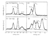
- Illustrative in respect of this embodiment may be Figure 2. Exemplary for this process, Figure 2 shows the core level spectra of X-ray photoelectron spectroscopy (XPS) of deposited molybdenum disulphide (MoS 2 ).
- the metal or metalloid chalcogenide may be prismatically coordinated by six surrounding chalcogen atoms and the c-axis may be perpendicular to the substrate.
- Illustrative in respect of this embodiment may be Figure 3.
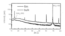
- Figure 3 shows a high-resolution X-ray diffraction result for MoS 2 film grown as compared to the bulk materials. The out-of-plane orientation of MoS 2 film was determined to be (0001). The crystal structure of the film is confirmed to be 2H-MoS 2 phase on the substrates [Al 2 O 3 (0001)] and YSZ(111).
- each molybdenum atom is prismatically coordinated by six surrounding sulphur atoms and it exhibits semiconducting behaviour.
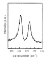
- Supplementing the result of the 2H-MoS 2 phase is also a Raman spectrum ( Figure 4), which additionally demonstrates that the films exhibit the correct phase and that they are in good quality.
- the process as disclosed herein may comprise the production of a transition metal dichalcogenide.
- the deposited metal or metalloid chalcogenide may have semi-conducting properties. These properties may include, but are not limited to, passing current more easily in one direction than the other, showing variable resistance, and sensitivity to light or heat. This is especially the case for 2D monolayers or multiple layers of a small number of suitable chalcogenides, such as. MoS 2 .
- the metal or metalloid may include, but is not limited to, metals or metalloids such as indium, silicon, germanium, silver, tin, lead, bismuth, antimony, strontium, and any alloys or mixtures of these elements. A combination of these elements from different groups, or from the same group, may be used.
- the metal or metalloid may include, but is not limited to, transition metals. It may include, but is not limited to, aluminium, chromium, copper, tungsten and molybdenum. A combination of these elements from different groups, or from the same group, may be used. These may be used in any desired mixing ratio.
- the metal may be a transition metal, such as tungsten or molybdenum, or a mixture of these in any mixing ratio.
- the metal or metalloid may be molybdenum.
- the process of the invention produces preferably transition metal dichalcogenides. Molybdenium and Tungsten dichalcogenieds or their mixtures can be especially mentioned.
- the sputtering target may include, but is not limited to, elemental molybdenum.
- the chalcogen may include, but is not limited to, sulphur, selenium and tellurium or mixtures thereof. These elements may have the advantage, that they produce a desirable band gap and therefore provide for the application of such coated substrates in, for example, field effect transistor devices.
- the chalcogen may be sulphur.
- the preferred chalcogenide can then be MoS 2 .
- the sulphur may be provided in the form of a powder for vaporization.
- This powder may be stored in a reservoir, wherein it is getting vaporized and, through a leaking valve, reach the deposition chamber.
- the growth rate of the metal or metalloid chalcogenide is, inter alia , dependant on the partial pressure of vaporized chalcogen. Therefore, it is understood, that the heating temperature of the reservoir may be adjusted depending on the chalcogen used.
- Vaporizing of the sulphur is preferably done in a controlled manner. For controlling the vaporization typical valves combined with an RGA can be used.
- chalcogenide monolayers obtainable by the process as defined above.
- the chalcogenide monolayers obtainable by the process have an organized structure of uniformity, although showing the presence of more lattice disorder or residual dopants than mechanically exfoliated monolayers. They are new materials for use in the applications mentioned throughout the description.
- a metal or metalloid chalcogenide as defined above in a layered semiconductor device, such as a field effect transistor.
- a thin layer of dichalcogenide is for instance well suited as a channel material in field effect transistors (FETs), exhibiting high mobility, almost ideal switching characteristics and low standby power dissipation.
- metal or metalloid chalcogenide as disclosed above in nanoelectronics as a catalyst, as a photo-detector, photovoltaic or photocatalyst.
- the photovoltaic or photocatalyst may be used in the range of visible light to near-infrared applications, preferably it may be used under visible light conditions.
- XPS X-ray photoelectron spectroscopy
- Non-limiting examples of the invention and a comparative example will be further described in greater detail by reference to specific examples, which should not be construed as in any way limiting the scope of the invention.
- the magnetron sputtering of molybdenum is carried out in a vaporized sulphur ambient.
- the sputtering gun is a Torus magnetron sputtering (TM3u) from K.J Lesker.
- the target is molybdenum (99.9% from Able Target).
- the chalcogenide is sulphur (99.5% sulphur powder, purchased from Sigma Aldrich).
- the power source is DC power.
- the substrates were pre-cleaned using acetone in an ultrasonic bath before introducing to the deposition chamber. The deposition was performed with a substrate temperature of 700°C.
- the out-of-plane orientation of MoS 2 film was determined to be (0001) by high-resolution x-ray diffraction (HR-XRD), recorded on a PANalytical X’pert pro with step size 0.1 degree, dwell time 0.2 second, and a range of 10-80 degree.
- Figure 2 shows the core-level XPS spectra of Mo 3 d and S 2 p on MoS 2 /Sapphire, and MoS 2 /YSZ systems, recorded on a VG ESCALAB 220i-XL with monochromated X-Ray and 10eV pass energy to achieve high resolution. As shown in Fig.
- each Mo atom is prismatically coordinated by six surrounding S atoms and it exhibits semiconducting behaviour.
- the films can be grown on variable substrates with the c-axis of MoS 2 perpendicular to the substrate surface. All these results demonstrate that the films exhibit correct phase and they are in good quality.
- Raman spectra were obtained on a single- gating micro-Raman spectrometer (Horiba-JY T64000) excited with 532 nm laser. The signal was collected through a 100 ⁇ objective, dispersed with a 1800 g/mm grating, and detected by a liquid nitrogen cooled charge-coupled device. Photoluminescence (PL) was obtained from the same micro-Raman spectrometer. The Si peak at 520 cm -1 was used for calibration in the experiments.
- This process can be easily applied to other metal or metalloid dichalcogenide film growth by switching the target between, for example, molybdenum and tungsten, and switching the vapor source between, for example, sulphur and selenium.
- metal or metalloid chalcogenides described in this disclosure may be useful as a facile and low-cost procedure for a high-yield preparation of the materials.
- Such metal or metalloid chalcogenides have a direct band gap, and can be used in electronics as transistors and in optics as emitters and detectors.
- the metal or metalloid chalcogenide monolayer crystal structure has no inversion center, which allows to access a new degree of freedom of charge carriers, namely the k-valley index, and to open up a new field of physics: valleytronics.
- the strong spin-orbit coupling in metal or metalloid chalcogenide monolayers lead to a spin-orbit splitting of hundreds meV in the valence band and a few meV in the conduction band, which allows control of the electron spin by tuning the excitation laser photon energy.
- the work on metal or metalloid chalcogenide monolayers is an emerging research and development field since the discovery of the direct bandgap and the potential applications of the very peculiar electron valley physics.
- the process according to the invention provides a new method for producing such monolayers on larger areas and is therefore suited for mass fabrication of the materials.
Landscapes
- Chemical & Material Sciences (AREA)
- Chemical Kinetics & Catalysis (AREA)
- Engineering & Computer Science (AREA)
- Materials Engineering (AREA)
- Mechanical Engineering (AREA)
- Metallurgy (AREA)
- Organic Chemistry (AREA)
- Physical Vapour Deposition (AREA)
- Photovoltaic Devices (AREA)
Abstract
The instant invention provides a process for making metal or metalloid dichalcogenides from a metal or metalloid and elemental chalcogen using magnetron sputtering. The process may comprise the steps of directing sputtering gas ions at a metal or metalloid target, reacting the ejected metal or metalloid atoms from the target surface with an elemental chalcogen vapor and assembling the metal or metalloid dichalcogenides on a substrate. It can be used to make thin films of the dichalcogenides which have a use in layered semiconductor devices. The process of the invention is suitable for upscaling to potentially make the films on a wafer level. Films on large areas with high uniformity have for instance been obtained utilizing the reaction of the metal or metalloid in an ambient of vaporized chalcogen under controlled conditions and with low growth rates. The process of the invention can be used to deposit two dimensional channels as part of field effect transistors. The materials made with the process in general can have a use in nanoelectronics as a catalyst, as a photo-detector, photovoltaic or photocatalyst.
Description
The present invention generally relates to a
process for making metal or metalloid chalcogenides as
nanostructured materials. The present invention also
relates to the use of the process to create one or
multiple 2D monolayers of the metal or metalloid
chalcogenide. It also relates to the use of the metal or
metalloid chalcogenides in a layered semiconductor
device such as a field effect transistor.
Recently, transition-metal dichalcogenides
(TMD), a class of layered semiconductor, have received
increased interests due to their wide applications in
nanoelectronics, catalyst, photo-detectors, photovoltaic
and photocatalyst. Among them, molybdenum disulphide
(MoS2) was a prototype for this class and has
been most widely investigated both experimentally and
theoretically. Monolayer MoS2 presents a
direct band gap (1.8 eV) at the K point of the Brillouin
zone, while in few-layer and bulk counterpart an
indirect band gap (1.2 eV) is observed. With the small
band gap energy and high light absorption in the visible
light range, MoS2 could be suitable for
applications in effective photovoltaic and
photocatalysts under visible light. A monolayer
MoS2 transistor has shown a high current
on-off ratio of 1 × 10⁹, high current density
and the negligible OFF current using mechanically
exfoliated flakes from bulk geological samples. This
indicates that the sensitivity of MoS2-based
field effect transistors (FETs) can be significantly
improved which is comparable to silicon-based
transistors and better than that from graphene ribbons.
In addition, logic circuits and amplifiers have also
been demonstrated recently using monolayer
MoS2. The structure of MoS2 is
formed by covalently bonded S-Mo-S two-dimensional (2D)
hexagonal atomic trilayer, which weakly bounds with
neighboring layers via van der Waals forces. In each
layer, the electrons and holes are intrinsically
confined in the 2-dimensional layer, which gives rise to
many unusual physical and chemical properties and offers
the advantages of superior vertical scaling for a
transistor topology. The potential of these materials
for low-cost flexible or transparent electronics that
could revolutionize technology is also very high, which
are valuable for demonstrating the promise of
MoS2 devices. With these advantages and
potential applications, large area of MoS2
layers manufacturing with an easily controlled manner is
greatly desired.
Monolayer of MoS2 was first
obtained by the mechanical exfoliation technique as
commonly used for graphene. However, the traditional
mechanical exfoliation method limits its usefulness in a
commercially viable device. Later, attempts to develop
more scalable techniques include solution-based
exfoliation, epitaxial growth, and soft sulphurization,
physical vapor deposition, sulphurization of molybdenum
oxides, hydrothermal synthesis, and electrochemical
lithiation process. Recently, it is reported that large
scale MoS2 can be obtained via chemical vapor
deposition (CVD) using a Mo film (or MoO3
powder) and sulphur powder as the reactants. However,
all the previous used methods are not capable to
integrate with device fabrication and MoS2
monolayer resulted from those chemical methods will
co-exist with some by-products. As the properties of
MoS2 materials strongly depend on the layer
number, the uniformity and controllability are extremely
important for the improvement of device performance.
Similar to graphene, the practical application
based on such 2D semiconducting materials also requires
the facile procedures for low-cost and high-yield
preparation of the materials.
There is therefore a need to provide a process
for the production of metal or metalloid chalcogenides
that overcomes, or at least ameliorates, one or more of
the disadvantages described above.
According to a first aspect, there is provided
a process for making metal or metalloid chalcogenides
from a metal or metalloid and an elemental chalcogen
using magnetron sputtering.
In one embodiment, the sputtering process may
comprise the steps of a) directing sputtering gas ions
at a target comprising a metal or metalloid, b) reacting
the ejected metal or metalloid atoms from the target
surface with an elemental chalcogen vapor and c)
assembling the metal or metalloid chalcogenides on a
substrate. This process may involve a chemical reaction
between the ejected metal or metalloid atoms and the
chalcogen and may therefore additionally be referred to
as a reactive sputtering process. Preferably, the
reactive gas comprises an elemental chalcogen vapor.
Advantageously the process according to the
invention allows producing metal or metalloid
chalcogenide films in a controlled way. Films can be
grown uniformly over large areas in the form of a few
layers of the metal or metalloid chalcogenide. The
method can be scaled up to large area sample
preparation. In this way it is compatible with industry
mass production techniques on wafer level.
In another embodiment, the sputtering may be
performed in an apparatus comprising: i) a vacuum
deposition chamber, ii) a sputtering target comprising
the metal or metalloid, iii) a reservoir of
elemental chalcogen optionally linked to a vaporizer,
iv) a power source to effect ejection of the metal or
metalloid and v) a substrate on which the deposition of
the metal or metalloid chalcogenide occurs.
Advantageously, the use of such apparatus
allows effectively reacting the elemental chalcogen with
the metal or metalloid during the sputtering to form the
films. In the apparatus the vaporization of the
elemental chalcogen can be further controlled by the
optional use of a suitable vaporizer. Different crystal
structure imperfections may be introduced as compared to
known methods. Advantageously, the sulphur can be
vaporized in a suitable manner using such apparatus when
temperatures and partial vapor pressure of the elemental
chalcogen are controlled. Advantageously, the
sputtering gas is provided with a fixed pressure of
about 1.0 × 10⁻⁴ to 3.0 × 10⁻³ mbar.
The deposition in the sputtering process may
be performed with a substrate temperature of between
about 300°C and 1000°C. Advantageously, a high
temperature leads to the deposition of the desired films.
In another embodiment, the chalcogen may be
vaporized by heating. The vaporized chalcogen may
preferably produce a partial pressure of about 1.0 to
9.0 × 10⁻⁷ mbar. Advantageously, a controlled
vaporization by heating and a controlled partial
pressure of the chalcogen can be utilized for optimal
deposition for various applications.
More advantageously, the process as disclosed
above may be performed using a DC power source, with a
DC power of less than 10 W for the sputtering.
Advantageously, the growth rate of the layers can be
controlled with high precision by the use of a low power
source for sputtering.
Advantageously, a very low partial argon
pressure and a low power source used in the magnetron
sputtering process allows to grow materials at a very
low rate in a controllable chalcogen vapor environment,
which can allow the control of 2D growth down to
monolayers with lower defects.
The process as disclosed herein may comprise
the production of a transition metal dichalcogenide.
In a second aspect, there is provided the use
of the process to create one or multiple 2D monolayers
of the transitional chalcogenide on a substrate.
Advantageously, the 2D monolayers can be produced in
high uniformity and precision.
In a third aspect, there is provided a metal
or metalloid chalcogenide obtainable by the process as
disclosed above. The chalcogenide can advantageously be
grown on various substrates with a defined orientation
(e.g. c-axis of MoS2 perpendicular to the
substrate surface) and high quality.
In a fourth aspect, there is provided use of
the metal or metalloid chalcogenide as disclosed above
in a layered semiconductor device, such as a field
effect transistor. Advantageously, the obtained field
effect transistors can show an improved performance when
being applied in photovoltaic or photocatalyst applications.
In a fifth aspect, there is provided use of
the metal or metalloid chalcogenide as disclosed above
in nanoelectronics, as a catalyst, as a photo-detector,
photovoltaic or photocatalyst.
The following words and terms used herein
shall have the meaning indicated:
The term ‘transition metal’ is to be
interpreted broadly to include any element in which the
filling of the outermost shell to eight electrons within
a periodic table is interrupted to bring the penultimate
shell from 8 to 18 or 32 electrons. Transition elements
may include, without limitation, scandium, titanium,
vanadium, chromium, manganese, iron, cobalt, nickel,
copper, zinc, ytterbium, zirconium, niobium, molybdenum,
silver, lanthanum, hafnium, tantalum, tungsten, rhenium,
rare-earth elements, cerium, praseodymium, neodymium,
promethium, samarium, europium, gadolinium, terbium,
dysprosium, holmium, erbium, thulium, yttrium, lutetium,
and rhodium. Included in this definition are
post-transition metals, which may refer to the metallic
elements in the periodic table located between the
transition metals (to their left) and the metalloids (to
their right). These elements may include gallium, indium
and thallium; tin and lead; and bismuth, cadmium and
mercury; and aluminium.
The term ‘2D monolayer’ or ‘2-dimensional
monolayer’ is to be interpreted broadly to include
substantially flat, two dimensional layers of the
chalcogenide on an atomic level. Flat thin films (“2D
films”) of such layers may have the thickness of one or
multiple monolayers of the metal or metalloid
chalcogenide. It may typically have a thickness of up to
10 nm.
The term ‘inert gas’ is to be interpreted
broadly to include any gas which does not form chemical
bonds when used in magnetron sputtering. Exemplary inert
gases include noble gases but may include other gases so
long as no chemical bonds are formed.
The term ‘chalcogen’ is to be interpreted
broadly to include Group VIA elements. Group VIA
elements may include sulphur, selenium and tellurium or
mixtures thereof.
The term ‘film’ is to be interpreted broadly
to include a thin, commonly flexible, form of a
material, which may be for example a layer on a surface
of a substrate.
The term ‘substrate’ is to be interpreted
broadly to include materials upon which one or more
layers of the metal or metalloid chalcogenide may be
deposited. The substrate may comprise any material, as
long as it is stable under the conditions applied in the
sputtering process.
The term ‘target’ is to be interpreted broadly
to include materials from which atoms may be ejected to
form a coating on a substrate. The ejected atoms from
the target may engage in subsequent reactions to form
covalent bonds. In the present context, the target may
include, but is not limited to, metals or metalloids or
materials comprising metals or metalloids or materials
comprising transition metals.
The term ‘transition metal dichalcogenide’ is
to be interpreted broadly to include materials that
comprise transition metals and Group VIA elements. There
may be a covalent bond between the transition metal and
the atoms of the dichalcogenide.
The term ‘magnetron sputtering’ is to be
interpreted broadly to include the ejection of atoms
from a surface as a consequence of ions impacting that
surface and, in some manner, imparting enough energy to
some surface atoms to overcome binding energies and
cause these atoms to be ejected. The term may include
‘reactive sputtering’.
The term ‘vapor’, ‘vaporized’ or ‘vaporizer’
is to be interpreted broadly to include a gaseous phase
of the element. As used herein, it refers to the gaseous
phase of the chalcogenide, wherein the concentration of
the chalcogenide in the atmosphere may be irrelevant.
The word “substantially” does not exclude
“completely” e.g. a composition which is “substantially
free” from Y may be completely free from Y. Where
necessary, the word “substantially” may be omitted from
the definition of the invention.
Unless specified otherwise, the terms
"comprising" and "comprise", and grammatical variants
thereof, are intended to represent "open" or "inclusive"
language such that they include recited elements but
also permit inclusion of additional, unrecited elements.
As used herein, the term "about", in the
context of concentrations of components of the
formulations, typically means +/- 5% of the stated
value, more typically +/- 4% of the stated value, more
typically +/- 3% of the stated value, more typically,
+/- 2% of the stated value, even more typically +/- 1%
of the stated value, and even more typically +/- 0.5% of
the stated value.
Throughout this disclosure, certain
embodiments may be disclosed in a range format. It
should be understood that the description in range
format is merely for convenience and brevity and should
not be construed as an inflexible limitation on the
scope of the disclosed ranges. Accordingly, the
description of a range should be considered to have
specifically disclosed all the possible sub-ranges as
well as individual numerical values within that range.
For example, description of a range such as from 1 to 6
should be considered to have specifically disclosed
sub-ranges such as from 1 to 3, from 1 to 4, from 1 to
5, from 2 to 4, from 2 to 6, from 3 to 6 etc., as well
as individual numbers within that range, for example, 1,
2, 3, 4, 5, and 6. This applies regardless of the
breadth of the range.
Certain embodiments may also be described
broadly and generically herein. Each of the narrower
species and subgeneric groupings falling within the
generic disclosure also form part of the disclosure.
This includes the generic description of the embodiments
with a proviso or negative limitation removing any
subject matter from the genus, regardless of whether or
not the excised material is specifically recited herein.
Exemplary, non-limiting embodiments of a
process for the production of a metal or metalloid
chalcogenide, will now be disclosed.
There is provided a one-step process for
making metal chalcogenides from a metal or metalloid and
an elemental chalcogen using magnetron sputtering. The
term sputtering refers to the ejection of atoms from the
surface of a target as a consequence of ions impacting
that surface and, in some manner, imparting enough
energy to some surface atoms to overcome binding
energies and cause these atoms to be ejected. Sputtering
is most commonly used as a method of depositing coatings
onto other surfaces.
The sputtering according to the invention
preferably provides for a target subjected to ion
bombardment (“ion-beam sputtering”). Additionally, the
atoms ejected from the target may engage in chemical
reactions (“reactive sputtering”) with a reactive gas of
the elemental chalcogen present in the process
(preferably a vaporized chalcogen) and thus the
deposited coating will have a different chemical
composition from the target. The items to be coated,
generally referred to as the substrates, are preferably
placed in locations (with respect to the ion bombarded
surface) in which their surfaces will intercept the
greatest flux of ejected atoms, and thus be coated. In
magnetron sputtering, magnetic fields are employed to
help confine electrons which generate the plasma which
is the source of bombarding ions. This confinement
greatly increases both the sputtering rate and the
system efficiency by minimizing the loss of both ions
and ionizing electrons.
The process may be applicable to large scale
production of the metal or metalloid chalcogenides. It
may be applicable to conventional present semiconductor
fabrication processes. It may be applicable for the
fabrication of 8 inch wafers.
Thus, in one embodiment, the process as
disclosed above may comprise the steps of a) directing
sputtering gas ions at a target comprising a metal or
metalloid (ion-beam sputtering), b) reacting the ejected
metal or metalloid atoms from the target surface with an
elemental chalcogen vapor (reactive sputtering) and c)
assembling the metal or metalloid chalcogenides on a
substrate.
Sputtering may be conducted in a vacuum
deposition chamber and in the presence of an inert
sputtering gas, such as argon, that may be maintained
under very low pressure. The inert sputtering gas may
form a plasma, which may contain a reactive gas, for
example elemental chalcogen, optionally linked to a
vaporizer. The material to be sputtered (referred to as
the target) may be connected to the negative terminal of
a DC power supply and may serve as a cathode. The
positive terminal of the power supply may be connected
to a separate anode structure or to the vacuum chamber
itself, depending on the application. Deposition of the
reaction product between the atoms originating from the
target and atoms originating from the reactive gas, in
the present context the metal or metalloid chalcogenide,
may occur on a substrate.
The target is preferably a metal or metalloid.
Thus, in one embodiment, the sputtering
process may be performed in an apparatus comprising: i)
a vacuum deposition chamber, ii) a sputtering target
comprising the metal or metalloid, iii) a
reservoir of elemental chalcogen optionally linked to a
vaporizer, iv) a power source to effect the ejection of
metal or metalloid atoms and v) a substrate on which the
deposition of the metal or metalloid chalcogenide
occurs. Illustrative in this context is Figure 1, in
which an exemplary apparatus is shown. It consists of a
chamber, which is connected to a pump for production of
a vacuum. Introduced into this chamber is a sputtering
target, from which atoms can be ejected. On the opposite
side and in a straight line of the sputtering target is
a substrate, on which the deposition of the metal or
metalloid chalcogenide may occur. Additionally connected
to the vacuum chamber is a reservoir, containing the
elemental chalcogen, provided as a powder according to a
preferred embodiment, which is wrapped in heating tape.
This effects small amounts of the chalcogen to evaporate
and, through a leaking valve, reach the vacuum chamber
in a vaporized state. The sputtering gas, in the example
shown as Argon, may be ionized and thereby ejecting
atoms from the sputtering target. The ejected atoms
originating from the sputtering may react with the
chalcogen and the reaction product may self-assemble on
the substrate, thereby forming a thin film, optionally a
monolayer. The process can be used to create such
monolayer, but also two layers, three layers, four
layers, five layers, six layers, seven layers or
multiple layers of small number, but controlled number
on the substrate by altering the power of the ion beam
or the deposition time.
In one embodiment, the process as disclosed
above may be performed with a substrate temperature of
between about 300 °C and about 1000°C, or between about
300 °C and about 900 °C, or between about 300 °C and
about 800 °C, or between about 300 °C and about 700 °C,
or between about 300 °C and about 600 °C, or between
about 300 °C and about 500 °C, or between about 300 °C
and about 400 °C, or between about 400 °C and about 1000
°C, or between about 500 °C and about 1000 °C, or
between about 600 °C and about 1000 °C, or between about
700 °C and about 1000 °C, or between about 800 °C and
about 1000 °C, or between about 900 °C and about 1000
°C, or between about 400 °C and about 900 °C, or between
about 500 °C and about 800 °C, or between about 600 °C
and about 800 °C, or preferably between about 650 °C and
about 750 °C, or at about 300 °C, at about 400 °C, at
about 500 °C, at about 600 °C, at about 700 °C, at about
800 °C, at about 00 °C, or at about 1000 °C. A
temperature of about 700 °C can be particularly
mentioned. For achieving a best uniformity it may be
desired to control the temperature in a small range.
In one embodiment, the chalcogen may be
vaporized by heating. The heating may be effected using
a variety of heat sources, which may include, but are
not limited to, heating tape, oil bath, sand bath, oven
or water bath. Advantageously, in one embodiment, the
heating of the chalcogen is performed by using wrapped
heating tape.
The heating process may result in the
vaporized chalcogen producing a partial pressure in the
vacuum chamber during the sputtering.
Thus, in one embodiment, the vaporized
chalcogen produces a partial pressure of about 1.0 to
about 9.0 × 10⁻⁷ mbar, or about 2.0 to about
9.0 × 10⁻⁷ mbar, or about 3.0 to about 9.0 ×
10-7 mbar, or about 4.0 to about 9.0 ×
10-7 mbar, or about 5.0 to about 9.0 ×
10-7 mbar, or about 6.0 to about 9.0 ×
10-7 mbar, or about 7.0 to about 9.0 ×
10-7 mbar, or about 8.0 to about 9.0 ×
10-7 mbar, or about 1.0 to about 8.0 ×
10-7 mbar, or about 1.0 to about 7.0 ×
10-7 mbar, or about 1.0 to about 6.0 ×
10-7 mbar, or about 1.0 to about 5.0 ×
10-7 mbar, or about 1.0 to about 4.0 ×
10-7 mbar, or about 1.0 to about 3.0 ×
10-7 mbar, or about 1.0 to about 2.0 ×
10-7 mbar, or about 2.0 to about 8.0 ×
10-7 mbar, or about 3.0 to about 7.0 ×
10-7 mbar, or about 4.0 to about 6.0 ×
10-7 mbar, or of about 1.0 × 10⁻⁷
mbar, of about 2.0 × 10⁻⁷ mbar, of about 3.0
× 10-7 mbar, of about 4.0 × 10⁻⁷
mbar, of about 5.0 × 10⁻⁷ mbar, of about 6.0
× 10-7 mbar, of about 7.0 × 10⁻⁷
mbar, of about 8.0 × 10⁻⁷ mbar, or of about
9.0 × 10⁻⁷ mbar. A range of about 3.0 to
about 5.0 × 10⁻⁷ mbar can be particularly
mentioned. It can be critical for optimal performance to
control this partial gas pressure carefully using for
instance a residual gas analyser (RGA). As a residual
gas analyse a small and usually rugged mass
spectrometer, typically designed for process control in
vacuum systems, can be used.
In one embodiment, the deposition chamber may
comprise a sputtering gas. As detailed further above,
sputtering may be conducted in the presence of a
sputtering gas, such as an inert gas, that
advantageously may be maintained under very low pressure.
The sputtering gas may be provided with a
fixed pressure of about 1.0 × 10⁻⁴ to about
3.0 × 10⁻³ mbar, or about 1.0 ×
10-4 to about 2.0 × 10⁻³ mbar, or
about 1.0 × 10⁻⁴ to about 1.0 ×
10-3 mbar, or about 1.0 × 10⁻⁴ to
about 9.0 × 10⁻⁴ mbar, or about 1.0 ×
10-4 to about 8.0 × 10⁻⁴ mbar, or
about 1.0 × 10⁻⁴ to about 7.0 ×
10-4 mbar, or about 1.0 × 10⁻⁴ to
about 6.0 × 10⁻⁴ mbar, or about 1.0 ×
10-4 to about 5.0 × 10⁻⁴ mbar, or
about 1.0 × 10⁻⁴ to about 4.0 ×
10-4 mbar, or about 1.0 × 10⁻⁴ to
about 3.0 × 10⁻⁴ mbar, or about 1.0 ×
10-4 to about 2.0 × 10⁻⁴ mbar, or
about 2.0 × 10⁻⁴ to about 3.0 ×
10-3 mbar, or about 3.0 × 10⁻⁴ to
about 3.0 × 10⁻³ mbar, or about 4.0 ×
10-4 to about 3.0 × 10⁻³ mbar, or
about 5.0 × 10⁻⁴ to about 3.0 ×
10-3 mbar, or about 6.0 × 10⁻⁴ to
about 3.0 × 10⁻³ mbar, or about 7.0 ×
10-4 to about 3.0 × 10⁻³ mbar, or
about 8.0 × 10⁻⁴ to about 3.0 ×
10-3 mbar, or about 9.0 × 10⁻⁴ to
about 3.0 × 10⁻³ mbar, or about 1.0 ×
10-3 to about 3.0 × 10⁻³ mbar, or
about 2.0 × 10⁻³ to about 3.0 ×
10-3 mbar, or about 2.0 × 10⁻⁴ to
about 2.0 × 10⁻³ mbar, or about 3.0 ×
10-4 to about 1.0 × 10⁻³ mbar, or
about 4.0 × 10⁻⁴ to about 9.0 ×
10-4 mbar, or about 5.0 × 10⁻⁴ to
about 8.0 × 10⁻⁴ mbar, or about 6.0 ×
10-4 to about 7.0 × 10⁻⁴ mbar, or
at about 1.0 × 10⁻⁴, at about 2.0 ×
10-4, at about 3.0 × 10⁻⁴, at
about 4.0 × 10⁻⁴, at about 5.0 ×
10-4, at about 6.0 × 10⁻⁴, at
about 7.0 × 10⁻⁴, at about 8.0 ×
10-4, at about 9.0 × 10⁻⁴, at
about 1.0 × 10⁻³ mbar, at about 2.0 ×
10-3 mbar, or at about 3.0 × 10⁻³
mbar. A range of about 6.2 to 6.6 × 10⁻⁴ mbar
may be particularly mentioned.
In one embodiment, the sputtering gas may
comprise an inert gas. The inert gas may be chosen from
any gas, which does not from covalent bonds with any of
the reaction partners of the above disclosed process. It
may typically be chosen from the group of noble gases.
It may be chosen depending on the atomic weight of the
target, which usually is close to the atomic weight of
the sputtering gas, so for sputtering light elements
neon is preferable, while for heavy elements krypton or
xenon are used.
In one embodiment, the inert gas may comprise
a noble gas, such as argon, neon, xenon, and krypton. In
particular, it may comprise argon. Advantageously, argon
may be supplied at a partial pressure in a range of
about 6.2 to 6.6 × 10⁻⁴ mbar.
In one embodiment, the power source to effect
ejections of the metal or metalloid atoms may be
selected from the power sources including, but not
limited to, DC power and RF power. It may be a DC power
source. It may be a RF power source.
Advantageously, there is provided a DC power
of less than 10 W for the sputtering. A low DC current
may be particularly suitable for a low growth rate of
the metal or metalloid chalcogenide. This in turn may
ensure an optimal degree of control over the sputtering
process, which may result in the desired uniform and
high quality modification of the metal or metalloid
chalcogenide.
The growth rate can be chosen to achieve a
deposition rate of about 0.1 to 5 nm, 0.1 to about 4
nm, or about 0.1 to about 3 nm, or about 0.2 to about 5
nm, or about 0.2 to about 4 nm, or about 0.2 to about 1
nm, or about 0.3 to about 3.5 nm, or about 0.4 to about
2 nm, or about 0.2 to about 0.8 nm per minute.
Preferably it is 0.4 to 0.8 nm/min. A deposition rate of
about 0.6 nm/min may be particularly mentioned.
In one embodiment, the substrate may be
cleaned prior to the sputtering process. This may ensure
sufficient purity of the metal or metalloid
chalcogenide.
In a further embodiment, the cleaning may
involve using acetone in an ultrasonic bath. The
ultrasonic effect may de-attach any impurities off the
surface of the substrate. Acetone may be preferably used
as it has been found to remove most impurities well and
it has the additional beneficial effect, that it
evaporates quickly and does not itself represent an impurity.
In one embodiment, the substrate may include,
but is not limited to, materials from the group
consisting of glass, silicon, silicon oxides, metal,
metal alloy, metal oxides and any mixture thereof. It
may include any material, which is substantially stable
under the reaction conditions. It may include materials
or devices in need of a coating film consisting of a 2D
monolayer or several well-defined layers of a metal or
metalloid chalcogenide. The substrate may function as a
substantially inert carrier.
In one embodiment, the substrate may include,
but is not limited to, silicon or silicon oxide,
optionally in amorphous phase and optionally
hafnia-stabilized. Alternatively, it may include, but is
not limited to, crystalline silicone. In this case the
process may have a suitable application in wafer
production.
In one embodiment, the substrate may include,
but is not limited to, corundum, optionally aluminium
oxide, preferably in a crystalline
polymorphic phase α-Al2O3 There
may be traces of other elements embedded in the
aluminium oxide, for example iron, titanium, chromium,
copper, or magnesium. Or it may be a gem stone, for
example sapphire, emerald or ruby. It may be a single
crystal of aluminium oxide. It may have a particular
orientation, for example, it may be a c-plane sapphire [Al2O3(0001)].
Alternatively, in one embodiment, the
substrate may include, but is not limited to, zirconia.
It may be a cubic zirconia. It may be an oxide of
zirconium. It may be a crystalline form of zirconia, or
it may an amorphous form of zirconia. It may be
stabilized by various other materials, to form
stabilized zirconias, including, but not limited to
calcia-, magnesia-, ceria-, hafnia or alumina-stabilized
zirconias, or it may be partially stabilized zirconias.
In a specific example, it may be yttria-stabilized
zirconia (YSZ).
In one embodiment, the metal or metalloid
chalcogenide may be a film on a substrate. The film may
be in the form of a layer on a surface of the substrate.
It may be a dry layer, as contrasted to a solution. The
adhesive strength between the substrate and the film may
be greater than the cohesive strength of the film. Thus
if sufficient force is applied, the film may fail within
its body rather than at the adhesive interface between
the film and the substrate. This ensures a suitable hold
between the surface of the substrate and the film.
In one embodiment, the film may include, but
is not limited to, one or multiple monolayers of the
metal or metalloid chalcogenides. The film therefore may
comprise a monolayer, two layers, three layers, four,
five layer, six layers, seven layers or a low number of
multiple layers of the dichalcogenide. The thickness may
vary according to the chalcogenides obtained in the
process.
Advantageously, the film may have a thickness
of about 0.5 to about 10 nm, or about 1.0 to about 10
nm, or about 2.0 to about 10 nm, or about 3.0 to about
10 nm, or about 4.0 to about 10 nm, or about 5.0 to
about 10 nm, or about 6.0 to about 10 nm, or about 7.0
to about 10 nm, or about 8.0 to about 10 nm, or about
9.0 to about 10 nm, or about 0.5 to about 9.0 nm, or
about 0.5 to about 8.0 nm, or about 0.5 to about 7.0 nm,
or about 0.5 to about 6.0 nm, or about 0.5 to about 5.0
nm, or about 0.5 to about 4.0 nm, or about 0.5 to about
3.0 nm, or about 0.5 to about 2.0 nm, or about 0.5 to
about 1.0 nm, or of about 0.5 nm, about 1.0 nm, about
2.0 nm, about 3.0 nm, about 4.0 nm, about 5.0 nm, about
6.0 nm, about 7.0 nm, about 8.0 nm, about 9.0 nm, or of
about 10 nm.
The monolayers may have a thickness of about
0.3 to 2 nm, about 0.5 to 1 nm or about 0.6 to 0.8 nm.
In the case of molybdenum dichalcogenide the thickness
of the monolayer is usually about 0.75 nm ± 20 %.
In some embodiments, the metal or metalloid
has an oxidation state of +4 and the atomic ratio
between the metal or metalloid and the chalcogen may be
between about 1:1.75 to 2.05, or about 1:1.75 to 1.95,
or about 1:1.75 to 1.85, or about 1:1.85 to 2.05, or
about 1:1.95 to 2.05, or about 1:1.75, about 1:1.85,
about 1:1.95, or about 1:2.05. Illustrative in respect
of this embodiment may be Figure 2. Exemplary for this
process, Figure 2 shows the core level spectra of X-ray
photoelectron spectroscopy (XPS) of deposited molybdenum
disulphide (MoS2). It elucidates the
molybdenum 3d and sulphur 2p spectra of
MoS2/sapphire (0001) [(a) and (b)], and
MoS2/YSZ (111) [(c) and (d)]. In this
example, a few layers of MoS2 were first
grown on c-plane sapphire
[Al2O3(0001)] and YSZ(111).
As shown in Figure 2 (a) and (c), the Mo 3d
spectra on both substrates are almost identical, which
can be fitted using two components at 229.81 and 232.94
eV, respectively, in agreement with reported values. As
shown in Figure 2 (b) and (d), the spin-orbital
splitting for S 2p is well resolved which suggest
the good film quality. On YSZ, the lower binding energy
peaks at 161.31 eV and 159.21 eV come from the Y 3d
3/2 and 3d
5/2 orbitals. The atomic ratio between Mo and
S is determined to be 1:2 from quantitative analysis of
the XPS peaks.
In the metal or metalloid chalcogenide, the
metal or metalloid may be prismatically coordinated by
six surrounding chalcogen atoms and the c-axis may be
perpendicular to the substrate. Illustrative in respect
of this embodiment may be Figure 3. Exemplary for the
process, Figure 3 shows a high-resolution X-ray
diffraction result for MoS2 film grown as
compared to the bulk materials. The out-of-plane
orientation of MoS2 film was determined to be
(0001). The crystal structure of the film is confirmed
to be 2H-MoS2 phase on the substrates
[Al2O3(0001)] and YSZ(111). In
this phase, each molybdenum atom is prismatically
coordinated by six surrounding sulphur atoms and it
exhibits semiconducting behaviour. Supplementing the
result of the 2H-MoS2 phase is also a Raman
spectrum (Figure 4), which additionally demonstrates
that the films exhibit the correct phase and that they
are in good quality.
The process as disclosed herein may comprise
the production of a transition metal dichalcogenide.
As mentioned further above, in some
embodiments, the deposited metal or metalloid
chalcogenide may have semi-conducting properties. These
properties may include, but are not limited to, passing
current more easily in one direction than the other,
showing variable resistance, and sensitivity to light or
heat. This is especially the case for 2D monolayers or
multiple layers of a small number of suitable
chalcogenides, such as. MoS2.
The metal or metalloid may include, but is not
limited to, metals or metalloids such as indium,
silicon, germanium, silver, tin, lead, bismuth,
antimony, strontium, and any alloys or mixtures of these
elements. A combination of these elements from different
groups, or from the same group, may be used. The metal
or metalloid may include, but is not limited to,
transition metals. It may include, but is not limited
to, aluminium, chromium, copper, tungsten and
molybdenum. A combination of these elements from
different groups, or from the same group, may be used.
These may be used in any desired mixing ratio. In
particular, the metal may be a transition metal, such as
tungsten or molybdenum, or a mixture of these in any
mixing ratio. Optionally, the metal or metalloid may be
molybdenum. In case that the metal is a transition metal
the process of the invention produces preferably
transition metal dichalcogenides. Molybdenium and
Tungsten dichalcogenieds or their mixtures can be
especially mentioned. In one embodiment, the sputtering
target may include, but is not limited to, elemental
molybdenum.
The chalcogen may include, but is not limited
to, sulphur, selenium and tellurium or mixtures thereof.
These elements may have the advantage, that they produce
a desirable band gap and therefore provide for the
application of such coated substrates in, for example,
field effect transistor devices.
In one embodiment, the chalcogen may be
sulphur. The preferred chalcogenide can then be MoS2.
The sulphur may be provided in the form of a
powder for vaporization. This powder may be stored in a
reservoir, wherein it is getting vaporized and, through
a leaking valve, reach the deposition chamber. The
growth rate of the metal or metalloid chalcogenide is,
inter alia, dependant on the partial pressure
of vaporized chalcogen. Therefore, it is understood,
that the heating temperature of the reservoir may be
adjusted depending on the chalcogen used. Vaporizing of
the sulphur is preferably done in a controlled manner.
For controlling the vaporization typical valves combined
with an RGA can be used.
There is provided the use of the process to
create one or multiple 2D monolayers of the transitional
chalcogenide on a substrate. Preferably, one, two,
three, four, five, six or seven layers are deposited
with well-defined structure.
There is provided a metal or metalloid
chalcogenide obtainable by the process as defined above.
The chalcogenide monolayers obtainable by the process
have an organized structure of uniformity, although
showing the presence of more lattice disorder or
residual dopants than mechanically exfoliated
monolayers. They are new materials for use in the
applications mentioned throughout the description.
In one embodiment there is provided the use of
the metal or metalloid chalcogenide as defined above in
a layered semiconductor device, such as a field effect
transistor. A thin layer of dichalcogenide is
for instance well suited as a channel material in field
effect transistors (FETs), exhibiting high mobility,
almost ideal switching characteristics and low standby
power dissipation.
There is provided use of the metal or
metalloid chalcogenide as disclosed above in
nanoelectronics, as a catalyst, as a photo-detector,
photovoltaic or photocatalyst.
The photovoltaic or photocatalyst may be used
in the range of visible light to near-infrared
applications, preferably it may be used under visible
light conditions.
The accompanying drawings illustrate a
disclosed embodiment and serves to explain the
principles of the disclosed embodiment. It is to be
understood, however, that the drawings are designed for
purposes of illustration only, and not as a definition
of the limits of the invention.
Non-limiting examples of the invention and a
comparative example will be further described in greater
detail by reference to specific examples, which should
not be construed as in any way limiting the scope of the invention.
The magnetron sputtering of molybdenum is
carried out in a vaporized sulphur ambient. The
sputtering gun is a Torus magnetron sputtering (TM3u)
from K.J Lesker. The target is molybdenum (99.9% from
Able Target). The chalcogenide is sulphur (99.5% sulphur
powder, purchased from Sigma Aldrich). The power source
is DC power. The substrates were pre-cleaned using
acetone in an ultrasonic bath before introducing to the
deposition chamber. The deposition was performed with a
substrate temperature of 700°C. Sulphur powder was
heated up above 250 °C by wrapped heating tape to obtain
the desired sulphur partial pressure, 4.0 ×
10−7 mbar in the present system. The argon
pressure is fixed at 6.0 × 10⁻⁴ mbar. Both
partial pressures were measured and monitored by RGA CIS
200 from SRS. The DC power is kept as low as 6 W for low
growth rate. Using this process, few layers of
MoS2 can be grown on variable substrates,
such as sapphire, yttria-stabilized zirconia (YSZ),
amorphous SiO2 and Si etc. To demonstrate the
process, few layers of MoS2 were first grown
on c-plane sapphire [Al2O3(0001)]
and YSZ(111). The out-of-plane orientation of
MoS2 film was determined to be (0001) by
high-resolution x-ray diffraction (HR-XRD), recorded on
a PANalytical X’pert pro with step size 0.1 degree,
dwell time 0.2 second, and a range of 10-80 degree.
Figure 2 shows the core-level XPS spectra of Mo
3d and S 2p on MoS2/Sapphire,
and MoS2/YSZ systems, recorded on a VG
ESCALAB 220i-XL with monochromated X-Ray and 10eV pass
energy to achieve high resolution. As shown in Fig. 2
(a) and (c), the Mo 3d spectra on both substrates
are almost identical, which can be fitted using two
components at 229.81 and 232.94 eV, respectively, in
agreement with reported values. As shown in Fig. 2 (b)
and (d), the spin-orbital splitting for S 2p is
well resolved which suggest the good film quality. On
YSZ, the lower binding energy peaks at 161.31 eV and
159.21 eV come from the Y 3d
3/2 and 3d
5/2 orbitals. The atomic ratio between Mo and
S is determined to be 1:2 from quantitatively analysis
of XPS peaks. In addition, HR-XRD was used and the
crystal structure is of the film confirmed to be
2H-MoS2 phase on both substrates. In this
phase, each Mo atom is prismatically coordinated by six
surrounding S atoms and it exhibits semiconducting
behaviour. As shown below by HR-XRD, (Fig. 3) and
Raman spectrum (Fig. 4), the films can be grown on
variable substrates with the c-axis of MoS2
perpendicular to the substrate surface. All these
results demonstrate that the films exhibit correct phase
and they are in good quality. Raman spectra were
obtained on a single- gating micro-Raman spectrometer
(Horiba-JY T64000) excited with 532 nm laser. The signal
was collected through a 100× objective, dispersed with a
1800 g/mm grating, and detected by a liquid nitrogen
cooled charge-coupled device. Photoluminescence (PL) was
obtained from the same micro-Raman spectrometer. The Si
peak at 520 cm-1 was used for calibration in
the experiments.
This process can be easily applied to other
metal or metalloid dichalcogenide film growth by
switching the target between, for example, molybdenum
and tungsten, and switching the vapor source between,
for example, sulphur and selenium.
The process for the production of metal or
metalloid chalcogenides described in this disclosure may
be useful as a facile and low-cost procedure for a
high-yield preparation of the materials. Such metal or
metalloid chalcogenides have a direct band gap, and can
be used in electronics as transistors and in optics as
emitters and detectors. The metal or metalloid
chalcogenide monolayer crystal structure has no
inversion center, which allows to access a new degree of
freedom of charge carriers, namely the k-valley index,
and to open up a new field of physics: valleytronics.
The strong spin-orbit coupling in metal or
metalloid chalcogenide monolayers lead to a spin-orbit
splitting of hundreds meV in the valence band and a few
meV in the conduction band, which allows control of the
electron spin by tuning the excitation laser photon energy.
The work on metal or metalloid chalcogenide
monolayers is an emerging research and development field
since the discovery of the direct bandgap and the
potential applications of the very peculiar electron
valley physics. The process according to the invention
provides a new method for producing such monolayers on
larger areas and is therefore suited for mass
fabrication of the materials.
It will be apparent that various other
modifications and adaptations of the invention will be
apparent to the person skilled in the art after reading
the foregoing disclosure without departing from the
spirit and scope of the invention and it is intended
that all such modifications and adaptations come within
the scope of the appended claims.
Claims (40)
- A process for making metal or metalloid chalcogenides from a metal or metalloid and an elemental chalcogen using magnetron sputtering.
- The process of claim 1 comprising the steps of
a) directing sputtering gas ions at a target comprising a metal or metalloid
b) reacting the ejected metal or metalloid atoms from the target surface with an elemental chalcogen vapor and
c) assembling the metal or metalloid chalcogenides on a substrate. - The process of claim 1, wherein sputtering is performed in an apparatus comprising:
i) a vacuum deposition chamber
ii) a sputtering target comprising the metal or metalloid
iii) a reservoir of elemental chalcogen optionally linked to a vaporizer
iv) a power source to effect ejection of the metal or metalloid atoms,
v) a substrate on which the deposition of the metal or metalloid chalcogenide occurs. - The process of claim 1, wherein the process is performed using a substrate for assembling the chalcogenide which is heated to temperatures of between about 300 °C and 1000°C.
- The process of claim 1, wherein the chalcogen is vaporized by heating.
- The process of claim 5, wherein the heating of the chalcogen is performed by using wrapped heating tape.
- The process of claim 5, wherein the vaporized chalcogen produces a partial pressure of about 1.0 to 9.0 × 10⁻⁷ mbar.
- The process of claim 1, wherein a sputtering gas is used.
- The process of claim 8, wherein the sputtering gas is provided with a fixed pressure of about 1.0 × 10⁻⁴ to 3.0 × 10⁻³ mbar.
- The process of claim 8, wherein the sputtering gas comprises an inert gas.
- The process of claim 10, wherein the inert gas comprises argon.
- The process of claim 1, wherein the power source to effect ejection of the metal or metalloid atoms comprises a DC power and a RF power source.
- The process of claim 12, wherein the power source to effect ejection of the metal or metalloid atoms comprises a DC power.
- The process of claim 13, wherein the DC power source with a power of less than 10 W is used for the sputtering.
- The process of claim 1, wherein a substrate is used which is cleaned prior to the sputtering process.
- The process of claim 15, wherein the cleaning involves using acetone in an ultrasonic bath.
- The process of claim 1, wherein a substrate is used which comprises materials from the group consisting of glass, silicon, silicon oxides, metal, metal alloy, metal oxides and any mixture thereof.
- The process of claim 17, wherein the substrate comprises silicon or silicon oxide, optionally in amorphous phase and optionally hafnia-stabilized.
- The process of claim 17, wherein the substrate comprises aluminium oxide.
- The process of claim 17, wherein the substrate comprises zirconia.
- The process of claim 1, wherein the metal or metalloid chalcogenide is deposited as a film on a substrate.
- The process of claim 21, wherein the film comprises one or multiple monolayers of the metal or metalloid chalcogenides.
- The process of claim 22, wherein the film has a thickness of about 0.5 to 10 nm.
- The process of claim 1, wherein the metal or metalloid has an oxidation state of +4 and the atomic ratio between the metal or metalloid and the chalcogen is between about 1:1.75 to 2.05.
- The process of claim 24, wherein in the metal or metalloid chalcogenide, the metal or metalloid is prismatically coordinated by six surrounding chalcogen atoms and the c-axis is perpendicular to the substrate used in the process.
- The process of claim 21, wherein the metal or metalloid chalcogenide has semi-conducting properties.
- The process of claim 1, wherein the metal or metalloid comprises a transition metal.
- The process of claim 27, wherein the transition metal comprises aluminium, chromium, copper, tungsten and molybdenum.
- The process of claim 27, wherein the transition metal comprises a metal that is selected from tungsten, molybdenum or a mixture thereof.
- The process of claim 29, wherein the transition metal comprises molybdenum.
- The process of claim 1, wherein a sputtering target is used that comprises elemental molybdenum.
- The process of claim 1, wherein the metal or metalloid chalcogenide comprises a transition metal dichalcogenide.
- The process of claim 1, wherein the chalcogen comprises sulphur, selenium, tellurium or a mixture thereof.
- The process of claim 33, wherein the chalcogen comprises sulphur.
- The process of claim 1, wherein the chalcogen is provided in the form of a powder for vaporization.
- Use of the process of claim 1 to create one or multiple 2D monolayers of the transitional chalcogenide on a substrate.
- A metal or metalloid chalcogenide obtainable by the process of claim 1.
- Use of the metal or metalloid chalcogenide of claim 37 in a layered semiconductor device.
- Use of the metal or metalloid chalcogenide of claim 37 in nanoelectronics as a catalyst, a photo-detector, a photovoltaic or photocatalyst.
- The use of claim 39 wherein the photovoltaic or photocatalyst is used under visible light conditions.
Priority Applications (2)
| Application Number | Priority Date | Filing Date | Title |
|---|---|---|---|
| US15/328,896 US20170218498A1 (en) | 2014-07-24 | 2015-07-23 | Process for depositing metal or metalloid chalcogenides |
| SG11201700604RA SG11201700604RA (en) | 2014-07-24 | 2015-07-23 | Process for depositing metal or metalloid chalcogenides |
Applications Claiming Priority (2)
| Application Number | Priority Date | Filing Date | Title |
|---|---|---|---|
| SG10201404379Q | 2014-07-24 | ||
| SG10201404379Q | 2014-07-24 |
Publications (1)
| Publication Number | Publication Date |
|---|---|
| WO2016013984A1 true WO2016013984A1 (en) | 2016-01-28 |
Family
ID=55163400
Family Applications (1)
| Application Number | Title | Priority Date | Filing Date |
|---|---|---|---|
| PCT/SG2015/050231 Ceased WO2016013984A1 (en) | 2014-07-24 | 2015-07-23 | Process for depositing metal or metalloid chalcogenides |
Country Status (3)
| Country | Link |
|---|---|
| US (1) | US20170218498A1 (en) |
| SG (1) | SG11201700604RA (en) |
| WO (1) | WO2016013984A1 (en) |
Cited By (4)
| Publication number | Priority date | Publication date | Assignee | Title |
|---|---|---|---|---|
| WO2018087281A1 (en) * | 2016-11-11 | 2018-05-17 | Danmarks Tekniske Universitet | Fabrication of large-area multi-element two-dimensional materials |
| WO2019050483A1 (en) * | 2017-09-11 | 2019-03-14 | Agency For Science, Technology And Research | A sputtering system and method |
| WO2021032947A1 (en) | 2019-08-16 | 2021-02-25 | University Of Southampton | Method and composition |
| US12245531B2 (en) | 2019-09-18 | 2025-03-04 | Agency For Science, Technology And Research | Resistive memory device structure based on stacked layers of nanocrystalline TMDCs |
Families Citing this family (2)
| Publication number | Priority date | Publication date | Assignee | Title |
|---|---|---|---|---|
| US20220199405A1 (en) * | 2020-12-18 | 2022-06-23 | Osram Opto Semiconductors Gmbh | Method for Producing a Semiconductor Body, A Semiconductor Body and an Optoelectronic Device |
| RU2765222C1 (en) * | 2020-12-30 | 2022-01-26 | Тхе Баттериес Сп. з о.о. | METHOD FOR FORMING A LiCoO2 FILM AND APPARATUS FOR IMPLEMENTATION THEREOF |
Citations (1)
| Publication number | Priority date | Publication date | Assignee | Title |
|---|---|---|---|---|
| US5370778A (en) * | 1992-11-19 | 1994-12-06 | Iowa State University Research Foundation, Inc. | Method for preparing basal oriented molybdenum disulfide (MoS2) thin films |
Family Cites Families (6)
| Publication number | Priority date | Publication date | Assignee | Title |
|---|---|---|---|---|
| US6488824B1 (en) * | 1998-11-06 | 2002-12-03 | Raycom Technologies, Inc. | Sputtering apparatus and process for high rate coatings |
| AU2003222669A1 (en) * | 2002-04-22 | 2003-11-03 | Yazaki Corporation | Electrical connectors incorporating low friction coatings and methods for making them |
| US8362220B2 (en) * | 2007-04-13 | 2013-01-29 | The Board Of Trustees Of The University Of Illinois | Metal complex compositions and methods for making metal-containing films |
| US8969720B2 (en) * | 2010-03-17 | 2015-03-03 | Dow Global Technologies Llc | Photoelectronically active, chalcogen-based thin film structures incorporating tie layers |
| WO2012012376A1 (en) * | 2010-07-22 | 2012-01-26 | First Solar, Inc | Deposition system |
| US8734619B1 (en) * | 2011-03-02 | 2014-05-27 | Hanergy Holding Group Ltd. | Method of sensing local sputtering target selenization |
-
2015
- 2015-07-23 SG SG11201700604RA patent/SG11201700604RA/en unknown
- 2015-07-23 US US15/328,896 patent/US20170218498A1/en not_active Abandoned
- 2015-07-23 WO PCT/SG2015/050231 patent/WO2016013984A1/en not_active Ceased
Patent Citations (1)
| Publication number | Priority date | Publication date | Assignee | Title |
|---|---|---|---|---|
| US5370778A (en) * | 1992-11-19 | 1994-12-06 | Iowa State University Research Foundation, Inc. | Method for preparing basal oriented molybdenum disulfide (MoS2) thin films |
Non-Patent Citations (1)
| Title |
|---|
| REDDY ET AL.: "Formation of polycrystalline SnS layers by a two-step process", THIN SOLID FILMS, vol. 403 - 40, 2002, pages 116 - 117 and 119 * |
Cited By (5)
| Publication number | Priority date | Publication date | Assignee | Title |
|---|---|---|---|---|
| WO2018087281A1 (en) * | 2016-11-11 | 2018-05-17 | Danmarks Tekniske Universitet | Fabrication of large-area multi-element two-dimensional materials |
| WO2019050483A1 (en) * | 2017-09-11 | 2019-03-14 | Agency For Science, Technology And Research | A sputtering system and method |
| US11257663B2 (en) | 2017-09-11 | 2022-02-22 | Agency For Science, Technology And Research | Sputtering system and method |
| WO2021032947A1 (en) | 2019-08-16 | 2021-02-25 | University Of Southampton | Method and composition |
| US12245531B2 (en) | 2019-09-18 | 2025-03-04 | Agency For Science, Technology And Research | Resistive memory device structure based on stacked layers of nanocrystalline TMDCs |
Also Published As
| Publication number | Publication date |
|---|---|
| SG11201700604RA (en) | 2017-02-27 |
| US20170218498A1 (en) | 2017-08-03 |
Similar Documents
| Publication | Publication Date | Title |
|---|---|---|
| Lin et al. | Controllable thin‐film approaches for doping and alloying transition metal dichalcogenides monolayers | |
| WO2016013984A1 (en) | Process for depositing metal or metalloid chalcogenides | |
| Reddy et al. | Structural, optical and XPS study of thermal evaporated In2O3 thin films | |
| Gao et al. | Repeated and controlled growth of monolayer, bilayer and few-layer hexagonal boron nitride on Pt foils | |
| Suzuki et al. | Growth of atomically thin hexagonal boron nitride films by diffusion through a metal film and precipitation | |
| Xu et al. | Wafer scale quasi single crystalline MoS2 realized by epitaxial phase conversion | |
| Cao et al. | Photocatalytic activity and photocorrosion of atomic layer deposited ZnO ultrathin films for the degradation of methylene blue | |
| US11869768B2 (en) | Method of forming transition metal dichalcogenide thin film | |
| EP3575436A1 (en) | Method for direct patterned growth of atomic layer transition metal dichalcogenides | |
| Azam et al. | Accelerated synthesis of atomically-thin 2D quantum materials by a novel laser-assisted synthesis technique | |
| KR20130020351A (en) | Fabricaion method of high-quality graphen film | |
| Kawamoto et al. | Micrometer-scale monolayer SnS growth by physical vapor deposition | |
| Saroja et al. | Optical studies of Ag2O thin film prepared by electron beam evaporation method | |
| US20210039949A1 (en) | Method and apparatus for producing a nanometer thick film of black phosphorus | |
| Youn et al. | Soft Sputtering of Large‐Area 2D MoS2 Layers Using Isolated Plasma Soft Deposition for Humidity Sensors | |
| Babenko et al. | Oxidising and carburising catalyst conditioning for the controlled growth and transfer of large crystal monolayer hexagonal boron nitride | |
| CN109437124B (en) | Method for synthesizing single-layer transition metal chalcogenide | |
| Fan et al. | Novel micro-rings of molybdenum disulfide (MoS 2) | |
| Ullah et al. | Continuous large area few layers MoS2 films by pulsed laser deposition and effect of annealing in sulfur environment | |
| KR102576569B1 (en) | Preparing method of transition metal dichalcogenide | |
| Sirghi | Plasma synthesis of photocatalytic TiO x thin films | |
| Tripathi et al. | Semiconductor oxide nanomaterial | |
| CN108441841B (en) | A kind of method of growing transition metal dichalcogenide thin film | |
| Musschoot et al. | ALD of vanadium oxide | |
| Thandavan et al. | Synthesis of ZnO nanowires via hotwire thermal evaporation of brass (CuZn) assisted by vapor phase transport of methanol |
Legal Events
| Date | Code | Title | Description |
|---|---|---|---|
| 121 | Ep: the epo has been informed by wipo that ep was designated in this application |
Ref document number: 15824945 Country of ref document: EP Kind code of ref document: A1 |
|
| DPE1 | Request for preliminary examination filed after expiration of 19th month from priority date (pct application filed from 20040101) | ||
| NENP | Non-entry into the national phase |
Ref country code: DE |
|
| WWE | Wipo information: entry into national phase |
Ref document number: 15328896 Country of ref document: US |
|
| 122 | Ep: pct application non-entry in european phase |
Ref document number: 15824945 Country of ref document: EP Kind code of ref document: A1 |