WO2015195052A1 - A method for bonding a chip to a wafer - Google Patents
A method for bonding a chip to a wafer Download PDFInfo
- Publication number
- WO2015195052A1 WO2015195052A1 PCT/SG2015/050173 SG2015050173W WO2015195052A1 WO 2015195052 A1 WO2015195052 A1 WO 2015195052A1 SG 2015050173 W SG2015050173 W SG 2015050173W WO 2015195052 A1 WO2015195052 A1 WO 2015195052A1
- Authority
- WO
- WIPO (PCT)
- Prior art keywords
- chip
- wafer
- bonding
- posts
- contacts
- Prior art date
- Legal status (The legal status is an assumption and is not a legal conclusion. Google has not performed a legal analysis and makes no representation as to the accuracy of the status listed.)
- Ceased
Links
Images





Classifications
-
- H—ELECTRICITY
- H10—SEMICONDUCTOR DEVICES; ELECTRIC SOLID-STATE DEVICES NOT OTHERWISE PROVIDED FOR
- H10W—GENERIC PACKAGES, INTERCONNECTIONS, CONNECTORS OR OTHER CONSTRUCTIONAL DETAILS OF DEVICES COVERED BY CLASS H10
- H10W90/00—Package configurations
-
- H—ELECTRICITY
- H10—SEMICONDUCTOR DEVICES; ELECTRIC SOLID-STATE DEVICES NOT OTHERWISE PROVIDED FOR
- H10W—GENERIC PACKAGES, INTERCONNECTIONS, CONNECTORS OR OTHER CONSTRUCTIONAL DETAILS OF DEVICES COVERED BY CLASS H10
- H10W72/00—Interconnections or connectors in packages
- H10W72/01—Manufacture or treatment
- H10W72/012—Manufacture or treatment of bump connectors, dummy bumps or thermal bumps
-
- H—ELECTRICITY
- H10—SEMICONDUCTOR DEVICES; ELECTRIC SOLID-STATE DEVICES NOT OTHERWISE PROVIDED FOR
- H10W—GENERIC PACKAGES, INTERCONNECTIONS, CONNECTORS OR OTHER CONSTRUCTIONAL DETAILS OF DEVICES COVERED BY CLASS H10
- H10W72/00—Interconnections or connectors in packages
- H10W72/01—Manufacture or treatment
- H10W72/012—Manufacture or treatment of bump connectors, dummy bumps or thermal bumps
- H10W72/01215—Manufacture or treatment of bump connectors, dummy bumps or thermal bumps forming coatings
-
- H—ELECTRICITY
- H10—SEMICONDUCTOR DEVICES; ELECTRIC SOLID-STATE DEVICES NOT OTHERWISE PROVIDED FOR
- H10W—GENERIC PACKAGES, INTERCONNECTIONS, CONNECTORS OR OTHER CONSTRUCTIONAL DETAILS OF DEVICES COVERED BY CLASS H10
- H10W72/00—Interconnections or connectors in packages
- H10W72/01—Manufacture or treatment
- H10W72/012—Manufacture or treatment of bump connectors, dummy bumps or thermal bumps
- H10W72/01231—Manufacture or treatment of bump connectors, dummy bumps or thermal bumps using blanket deposition
- H10W72/01233—Manufacture or treatment of bump connectors, dummy bumps or thermal bumps using blanket deposition in liquid form, e.g. spin coating, spray coating or immersion coating
- H10W72/01235—Manufacture or treatment of bump connectors, dummy bumps or thermal bumps using blanket deposition in liquid form, e.g. spin coating, spray coating or immersion coating by plating, e.g. electroless plating or electroplating
-
- H—ELECTRICITY
- H10—SEMICONDUCTOR DEVICES; ELECTRIC SOLID-STATE DEVICES NOT OTHERWISE PROVIDED FOR
- H10W—GENERIC PACKAGES, INTERCONNECTIONS, CONNECTORS OR OTHER CONSTRUCTIONAL DETAILS OF DEVICES COVERED BY CLASS H10
- H10W72/00—Interconnections or connectors in packages
- H10W72/01—Manufacture or treatment
- H10W72/012—Manufacture or treatment of bump connectors, dummy bumps or thermal bumps
- H10W72/01251—Changing the shapes of bumps
-
- H—ELECTRICITY
- H10—SEMICONDUCTOR DEVICES; ELECTRIC SOLID-STATE DEVICES NOT OTHERWISE PROVIDED FOR
- H10W—GENERIC PACKAGES, INTERCONNECTIONS, CONNECTORS OR OTHER CONSTRUCTIONAL DETAILS OF DEVICES COVERED BY CLASS H10
- H10W72/00—Interconnections or connectors in packages
- H10W72/01—Manufacture or treatment
- H10W72/012—Manufacture or treatment of bump connectors, dummy bumps or thermal bumps
- H10W72/01251—Changing the shapes of bumps
- H10W72/01255—Changing the shapes of bumps by using masks
-
- H—ELECTRICITY
- H10—SEMICONDUCTOR DEVICES; ELECTRIC SOLID-STATE DEVICES NOT OTHERWISE PROVIDED FOR
- H10W—GENERIC PACKAGES, INTERCONNECTIONS, CONNECTORS OR OTHER CONSTRUCTIONAL DETAILS OF DEVICES COVERED BY CLASS H10
- H10W72/00—Interconnections or connectors in packages
- H10W72/01—Manufacture or treatment
- H10W72/016—Manufacture or treatment of strap connectors
-
- H—ELECTRICITY
- H10—SEMICONDUCTOR DEVICES; ELECTRIC SOLID-STATE DEVICES NOT OTHERWISE PROVIDED FOR
- H10W—GENERIC PACKAGES, INTERCONNECTIONS, CONNECTORS OR OTHER CONSTRUCTIONAL DETAILS OF DEVICES COVERED BY CLASS H10
- H10W72/00—Interconnections or connectors in packages
- H10W72/01—Manufacture or treatment
- H10W72/019—Manufacture or treatment of bond pads
- H10W72/01931—Manufacture or treatment of bond pads using blanket deposition
- H10W72/01938—Manufacture or treatment of bond pads using blanket deposition in gaseous form, e.g. by CVD or PVD
-
- H—ELECTRICITY
- H10—SEMICONDUCTOR DEVICES; ELECTRIC SOLID-STATE DEVICES NOT OTHERWISE PROVIDED FOR
- H10W—GENERIC PACKAGES, INTERCONNECTIONS, CONNECTORS OR OTHER CONSTRUCTIONAL DETAILS OF DEVICES COVERED BY CLASS H10
- H10W72/00—Interconnections or connectors in packages
- H10W72/01—Manufacture or treatment
- H10W72/019—Manufacture or treatment of bond pads
- H10W72/01951—Changing the shapes of bond pads
-
- H—ELECTRICITY
- H10—SEMICONDUCTOR DEVICES; ELECTRIC SOLID-STATE DEVICES NOT OTHERWISE PROVIDED FOR
- H10W—GENERIC PACKAGES, INTERCONNECTIONS, CONNECTORS OR OTHER CONSTRUCTIONAL DETAILS OF DEVICES COVERED BY CLASS H10
- H10W72/00—Interconnections or connectors in packages
- H10W72/01—Manufacture or treatment
- H10W72/019—Manufacture or treatment of bond pads
- H10W72/01951—Changing the shapes of bond pads
- H10W72/01953—Changing the shapes of bond pads by etching
-
- H—ELECTRICITY
- H10—SEMICONDUCTOR DEVICES; ELECTRIC SOLID-STATE DEVICES NOT OTHERWISE PROVIDED FOR
- H10W—GENERIC PACKAGES, INTERCONNECTIONS, CONNECTORS OR OTHER CONSTRUCTIONAL DETAILS OF DEVICES COVERED BY CLASS H10
- H10W72/00—Interconnections or connectors in packages
- H10W72/01—Manufacture or treatment
- H10W72/0198—Manufacture or treatment batch processes
-
- H—ELECTRICITY
- H10—SEMICONDUCTOR DEVICES; ELECTRIC SOLID-STATE DEVICES NOT OTHERWISE PROVIDED FOR
- H10W—GENERIC PACKAGES, INTERCONNECTIONS, CONNECTORS OR OTHER CONSTRUCTIONAL DETAILS OF DEVICES COVERED BY CLASS H10
- H10W72/00—Interconnections or connectors in packages
- H10W72/071—Connecting or disconnecting
- H10W72/072—Connecting or disconnecting of bump connectors
-
- H—ELECTRICITY
- H10—SEMICONDUCTOR DEVICES; ELECTRIC SOLID-STATE DEVICES NOT OTHERWISE PROVIDED FOR
- H10W—GENERIC PACKAGES, INTERCONNECTIONS, CONNECTORS OR OTHER CONSTRUCTIONAL DETAILS OF DEVICES COVERED BY CLASS H10
- H10W72/00—Interconnections or connectors in packages
- H10W72/071—Connecting or disconnecting
- H10W72/072—Connecting or disconnecting of bump connectors
- H10W72/07211—Treating the bond pad before connecting, e.g. by applying flux or cleaning
-
- H—ELECTRICITY
- H10—SEMICONDUCTOR DEVICES; ELECTRIC SOLID-STATE DEVICES NOT OTHERWISE PROVIDED FOR
- H10W—GENERIC PACKAGES, INTERCONNECTIONS, CONNECTORS OR OTHER CONSTRUCTIONAL DETAILS OF DEVICES COVERED BY CLASS H10
- H10W72/00—Interconnections or connectors in packages
- H10W72/071—Connecting or disconnecting
- H10W72/072—Connecting or disconnecting of bump connectors
- H10W72/07231—Techniques
- H10W72/07232—Compression bonding, e.g. thermocompression bonding
-
- H—ELECTRICITY
- H10—SEMICONDUCTOR DEVICES; ELECTRIC SOLID-STATE DEVICES NOT OTHERWISE PROVIDED FOR
- H10W—GENERIC PACKAGES, INTERCONNECTIONS, CONNECTORS OR OTHER CONSTRUCTIONAL DETAILS OF DEVICES COVERED BY CLASS H10
- H10W72/00—Interconnections or connectors in packages
- H10W72/071—Connecting or disconnecting
- H10W72/072—Connecting or disconnecting of bump connectors
- H10W72/07231—Techniques
- H10W72/07236—Soldering or alloying
-
- H—ELECTRICITY
- H10—SEMICONDUCTOR DEVICES; ELECTRIC SOLID-STATE DEVICES NOT OTHERWISE PROVIDED FOR
- H10W—GENERIC PACKAGES, INTERCONNECTIONS, CONNECTORS OR OTHER CONSTRUCTIONAL DETAILS OF DEVICES COVERED BY CLASS H10
- H10W72/00—Interconnections or connectors in packages
- H10W72/20—Bump connectors, e.g. solder bumps or copper pillars; Dummy bumps; Thermal bumps
- H10W72/241—Dispositions, e.g. layouts
-
- H—ELECTRICITY
- H10—SEMICONDUCTOR DEVICES; ELECTRIC SOLID-STATE DEVICES NOT OTHERWISE PROVIDED FOR
- H10W—GENERIC PACKAGES, INTERCONNECTIONS, CONNECTORS OR OTHER CONSTRUCTIONAL DETAILS OF DEVICES COVERED BY CLASS H10
- H10W72/00—Interconnections or connectors in packages
- H10W72/20—Bump connectors, e.g. solder bumps or copper pillars; Dummy bumps; Thermal bumps
- H10W72/241—Dispositions, e.g. layouts
- H10W72/242—Dispositions, e.g. layouts relative to the surface, e.g. recessed, protruding
-
- H—ELECTRICITY
- H10—SEMICONDUCTOR DEVICES; ELECTRIC SOLID-STATE DEVICES NOT OTHERWISE PROVIDED FOR
- H10W—GENERIC PACKAGES, INTERCONNECTIONS, CONNECTORS OR OTHER CONSTRUCTIONAL DETAILS OF DEVICES COVERED BY CLASS H10
- H10W72/00—Interconnections or connectors in packages
- H10W72/20—Bump connectors, e.g. solder bumps or copper pillars; Dummy bumps; Thermal bumps
- H10W72/241—Dispositions, e.g. layouts
- H10W72/244—Dispositions, e.g. layouts relative to underlying supporting features, e.g. bond pads, RDLs or vias
-
- H—ELECTRICITY
- H10—SEMICONDUCTOR DEVICES; ELECTRIC SOLID-STATE DEVICES NOT OTHERWISE PROVIDED FOR
- H10W—GENERIC PACKAGES, INTERCONNECTIONS, CONNECTORS OR OTHER CONSTRUCTIONAL DETAILS OF DEVICES COVERED BY CLASS H10
- H10W72/00—Interconnections or connectors in packages
- H10W72/20—Bump connectors, e.g. solder bumps or copper pillars; Dummy bumps; Thermal bumps
- H10W72/241—Dispositions, e.g. layouts
- H10W72/245—Dispositions, e.g. layouts of outermost layers of multilayered bumps, e.g. bump coating being only on a part of a bump core
-
- H—ELECTRICITY
- H10—SEMICONDUCTOR DEVICES; ELECTRIC SOLID-STATE DEVICES NOT OTHERWISE PROVIDED FOR
- H10W—GENERIC PACKAGES, INTERCONNECTIONS, CONNECTORS OR OTHER CONSTRUCTIONAL DETAILS OF DEVICES COVERED BY CLASS H10
- H10W72/00—Interconnections or connectors in packages
- H10W72/20—Bump connectors, e.g. solder bumps or copper pillars; Dummy bumps; Thermal bumps
- H10W72/251—Materials
- H10W72/252—Materials comprising solid metals or solid metalloids, e.g. PbSn, Ag or Cu
-
- H—ELECTRICITY
- H10—SEMICONDUCTOR DEVICES; ELECTRIC SOLID-STATE DEVICES NOT OTHERWISE PROVIDED FOR
- H10W—GENERIC PACKAGES, INTERCONNECTIONS, CONNECTORS OR OTHER CONSTRUCTIONAL DETAILS OF DEVICES COVERED BY CLASS H10
- H10W72/00—Interconnections or connectors in packages
- H10W72/20—Bump connectors, e.g. solder bumps or copper pillars; Dummy bumps; Thermal bumps
- H10W72/251—Materials
- H10W72/255—Materials of outermost layers of multilayered bumps, e.g. material of a coating
-
- H—ELECTRICITY
- H10—SEMICONDUCTOR DEVICES; ELECTRIC SOLID-STATE DEVICES NOT OTHERWISE PROVIDED FOR
- H10W—GENERIC PACKAGES, INTERCONNECTIONS, CONNECTORS OR OTHER CONSTRUCTIONAL DETAILS OF DEVICES COVERED BY CLASS H10
- H10W72/00—Interconnections or connectors in packages
- H10W72/20—Bump connectors, e.g. solder bumps or copper pillars; Dummy bumps; Thermal bumps
- H10W72/29—Bond pads specially adapted therefor
-
- H—ELECTRICITY
- H10—SEMICONDUCTOR DEVICES; ELECTRIC SOLID-STATE DEVICES NOT OTHERWISE PROVIDED FOR
- H10W—GENERIC PACKAGES, INTERCONNECTIONS, CONNECTORS OR OTHER CONSTRUCTIONAL DETAILS OF DEVICES COVERED BY CLASS H10
- H10W72/00—Interconnections or connectors in packages
- H10W72/90—Bond pads, in general
-
- H—ELECTRICITY
- H10—SEMICONDUCTOR DEVICES; ELECTRIC SOLID-STATE DEVICES NOT OTHERWISE PROVIDED FOR
- H10W—GENERIC PACKAGES, INTERCONNECTIONS, CONNECTORS OR OTHER CONSTRUCTIONAL DETAILS OF DEVICES COVERED BY CLASS H10
- H10W72/00—Interconnections or connectors in packages
- H10W72/90—Bond pads, in general
- H10W72/921—Structures or relative sizes of bond pads
- H10W72/923—Bond pads having multiple stacked layers
-
- H—ELECTRICITY
- H10—SEMICONDUCTOR DEVICES; ELECTRIC SOLID-STATE DEVICES NOT OTHERWISE PROVIDED FOR
- H10W—GENERIC PACKAGES, INTERCONNECTIONS, CONNECTORS OR OTHER CONSTRUCTIONAL DETAILS OF DEVICES COVERED BY CLASS H10
- H10W72/00—Interconnections or connectors in packages
- H10W72/90—Bond pads, in general
- H10W72/951—Materials of bond pads
- H10W72/952—Materials of bond pads comprising metals or metalloids, e.g. PbSn, Ag or Cu
-
- H—ELECTRICITY
- H10—SEMICONDUCTOR DEVICES; ELECTRIC SOLID-STATE DEVICES NOT OTHERWISE PROVIDED FOR
- H10W—GENERIC PACKAGES, INTERCONNECTIONS, CONNECTORS OR OTHER CONSTRUCTIONAL DETAILS OF DEVICES COVERED BY CLASS H10
- H10W90/00—Package configurations
- H10W90/701—Package configurations characterised by the relative positions of pads or connectors relative to package parts
- H10W90/721—Package configurations characterised by the relative positions of pads or connectors relative to package parts of bump connectors
- H10W90/722—Package configurations characterised by the relative positions of pads or connectors relative to package parts of bump connectors between stacked chips
-
- H—ELECTRICITY
- H10—SEMICONDUCTOR DEVICES; ELECTRIC SOLID-STATE DEVICES NOT OTHERWISE PROVIDED FOR
- H10W—GENERIC PACKAGES, INTERCONNECTIONS, CONNECTORS OR OTHER CONSTRUCTIONAL DETAILS OF DEVICES COVERED BY CLASS H10
- H10W90/00—Package configurations
- H10W90/701—Package configurations characterised by the relative positions of pads or connectors relative to package parts
- H10W90/721—Package configurations characterised by the relative positions of pads or connectors relative to package parts of bump connectors
- H10W90/724—Package configurations characterised by the relative positions of pads or connectors relative to package parts of bump connectors between a chip and a stacked insulating package substrate, interposer or RDL
Definitions
- the present disclosure provides a method for bonding one or more chips to a wafer.
- a chip on wafer (CoW) bonding process involves the formation of copper (Cu) pillars on either the chip or the wafer, or both, before the chip is bonded to the wafer. If one of the chip and wafer does not include Cu pillars, it is instead provided with a Cu pad for bonding to the Cu pillars of the other of the chip and wafer.
- Cu copper
- the following discussion will be limited to arrangements where there are pairs of opposing Cu pillars – i.e. the chip and wafer each have Cu pillars, with each Cu pillar of the chip aligning with a unique Cu pillar of the wafer – though the same discussion applies when bonding a Cu pillar to a Cu pad.
- Each Cu pillar consists of a Cu post and a solder cap.
- the solder cap is typically applied using electroplating, followed by a reflow process to round the cap.
- the solder caps of the chip melt and react with solder caps of the wafer to permanently fix the chip to the wafer.
- the Cu pillars vary in height. This is the result of variance in the height of the Cu post and, or alternatively, the solder cap. As a consequence, thick solder caps are used, since solder deforms easily when melted, and pressure is usually applied to urge the chip against the wafer to ensure each Cu pillar meets and bonds with an opposing Cu pillar. This pressure can squeeze solder between the opposing Cu pillars. If the solder volume is large and the separation between Cu pillars (the “pitch”) is small, spreading solder can bridge neighbouring Cu pillars.
- Flip chip bonding – a process that can permanently bond a chip to a wafer in a single step — requires thick solder caps to ensure there is sufficient solder on each of the chip and wafer so that opposing Cu pillars can bond through formation of an intermetallic alloy between the opposing pillars.
- a thick solder cap is considered useful since the solder of a Cu pillar diffuses into the Cu post at elevated temperatures. This diffusion reduces the amount of available solder for the bonding process. Also, to form a smooth solder cap using a reflow process – the smoothness being necessary to ensure proper bonding and to reduce the impact of Cu pillar height variation – a relative thick minimum thickness is usually required.
- the present invention provides a method for chip on wafer bonding, comprising forming a plurality of posts on at least one of a chip and a wafer, and a like plurality of contacts on the other of the chip and the wafer; planarizing a contact surface of each post, the planarized contact surface having a surface roughness height; applying, to at least one of the chip and the wafer, a bonding material of a thickness no greater than the surface roughness height; temporarily bonding the posts to the contacts using the bonding material to stabilize a position of the chip relative to the wafer for permanent diffusion bonding of the chip to the wafer.
- the method may further include the step of permanently bonding the chip to the wafer by diffusion of the posts and contacts into each other.
- the present invention also provides an integrated chip formed using the method described above.
- surface roughness height refers to the difference in height between the lowest point on a surface and the highest point on the surface.
- the lowest point of a contact surface of a post on a wafer or chip is the point on that contact surface that is closest to the wafer or chip.
- the highest point of a contact surface of a post on a wafer or chip is the point on that contact surface that is furthest from the wafer or chip.
- temporary integrated chip refers to a chip and wafer that have been temporarily bonded in advance of being permanently bonded.
- temporary bonding refers to a condition in which the contact surface of a post is only partially bonded to an opposing contact. In other words, across the contact surface of the post there are regions in which the post is bonded to the opposing contact and regions where it is not, such that a reliable electrical connection has not been formed.
- opposite contact identify, for a post or contact on one of the chip and wafer, the post or contact on the other of the chip and wafer to which it will be bonded.
- contact surface refers to the surface of a contact (e.g. a post) that is to be bonded to an opposing contact.
- low melting point metal will be understood to mean a metal having a lower melting point than the material from which the contacts of the chip and wafer are fabricated.
- the contacts are formed from Cu, aluminium (Al) or gold (Au)
- the bonding material is formed from a lower melting point metal such as tin (Sn), indium (In), lead (Pb) or bismuth (Bi).
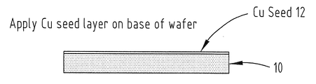
- Figure 1 is a side view of a wafer on which a Cu seed layer has been deposited
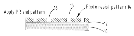
- Figure 2 is a side view of the wafer of Figure 1, with a photoresist layer in place;
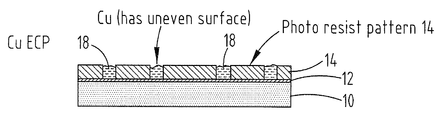
- Figure 3 is a side view of the wafer of Figure 2, after post deposition
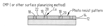
- Figure 4 is a side view of the wafer of Figure 3, after planarization;
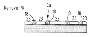
- Figure 5 is a side view of the wafer of Figure 4, after removal of the photoresist layer;
- Figure 6 is a side view of the wafer of Figure 5, after etching
- Figure 7 is a side view of the wafer of Figure 6, after bonding material deposition
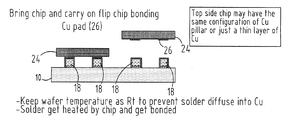
- Figure 8 is a side view of the wafer of Figure 7, with a first chip in register with some of the posts on the wafer and a second chip being brought into register with other posts on the wafer;
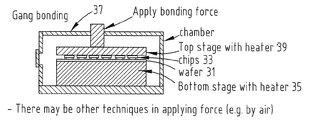
- Figure 9 is a side, cross-sectional view of a gang bonder with a single wafer in position on the bottom stage, ready for permanent bonding with multiple chips;
- Figure 10 is a plan view of a full wafer to which a number of chips have been temporarily bonded
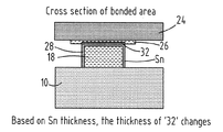
- Figure 11 is a side, close-up view of a bonding region between a post and pad
- Figures 12(a), 12(b) and 12(c) show progressive steps of a flip chip bonder picking up a chip, dipping it in an electroless solvent bath and then bringing the chip into register with a wafer;
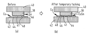
- Figures 13(a) and 13(b) show before and after illustrations of a chip and wafer being temporarily bonded using an electroless solvent
- Figures 14(a) and 14(b) show before and after illustrations of a chip and wafer being temporarily bonded using an electroless solvent with eutectic bonding to achieve temporary bonding of the chip to the wafer;
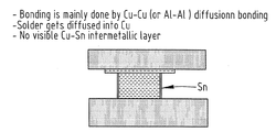
- Figure 15 shows a close-up view of a bonding region between a post and pad resulting from use of electroless solvent as a bonding material for temporary bonding.
- Figure 1 shows a wafer 10.
- An electrically conductive material seed layer 12 is deposited onto the wafer 10.
- the wafer 10 is formed from silicon. However, any other appropriate material may be used, such as germanium.
- Deposition of the seed layer 12 is performed using physical vapour deposition (PVD). This process produces very smooth layer of electrically conductive material having a surface roughness height of around 1nm.
- the electrically conductive material deposited by the PVD process may be Cu, Al, Au or any other appropriate material.
- the present seed layer 12 is formed from Cu.
- a photoresist 14 is laid over the seed layer 12 as shown in Figure 2.
- the photoresist 14 is patterned with the apertures 16 defining the positions where posts will be formed on the wafer 10.
- Posts 18 are then formed on the exposed portions of the seed layer 12, through the patterned photoresist 14, as shown in Figure 3.
- the present posts 18 are formed using an electroplating process.
- the posts 18 comprise the same electrically conductive material as the seed layer 12.
- the posts 18 are formed from Cu. While different metals can be used for the seed layer 12 and posts 18, using the same metals is useful. This ensures the melting point of the metals is the same and reduces the likelihood of galvanic corrosion.
- the posts 18 have irregular surfaces and dissimilar heights after electroplating. In prior art CoW bonding methods, this is one of the primary reasons for applying a thick layer of solder on the posts so that there is sufficient solder on each post for solder reflow to form a smooth cap.
- posts may be formed on either the chip and wafer or, in some embodiments, on both the chip and wafer.
- the posts 18 then undergo planarization.
- the planarization process results in a highly polished or planar contact surface on each of the posts 18.
- Planarization can be achieved using any process providing an appropriate low surface roughness (e.g. less than 20nm). Some relevant processes involve chemical-mechanical planarization (CMP) of the top surfaces 20 of the posts 18 using a CMP device (not shown). CMP can yield a surface roughness as low as 1nm. An different relevant process is bit grinding. Bit grinding can yield a surface roughness in the range of about 15 to 20nm. A further relevant process is dry polishing. Dry polishing can yield a surface roughness in the range of about 15 to 20nm. Whichever appropriate planarization process is adopted, it can be useful for the photoresist 14 to remain in place during planarization to reduce the likelihood of damage to the posts 18 resulting from lateral forces (i.e.
- CMP chemical-mechanical planarization
- lateral force may be applied by the carrier or chuck of the CMP device.
- the photoresist 14 provides lateral support to the posts 18 to counteract lateral forces applied during planarization. Accordingly, in the present embodiment, planarization occurs while the photoresist 14 is in place on the seed layer 12.
- Planarization removes material from the posts 18 until a desired height of the posts 18 is reached.
- the desired height will usually be the lowest part of the top surface 20 – in other words, the part of the contact surface closest to the wafer 10 before planarization – or lower. Electroplating often results in the lowest part of the top surface 20 being within the aperture 16 of the photoresist 14 – in other words, below the exposed surface of the photoresist 14. It is therefore usually necessary to also remove part of the photoresist 14 down to the desired height of the posts 18 after planarization, as shown in Figure 4 in which the photoresist 14 and posts 18 have undergone planarization until they form a substantially continuous, planar surface 22.
- planarization also results in uniform height of the posts 18 across the wafer. The uniformity in post height reduces the likelihood that chips will drift under applied pressure during subsequent permanent bonding.
- the top surface 20 is a contact surface that, after planarization, becomes better suited to contacting an opposing contact on the chip during CoW bonding according to the methods described herein.
- the contact surface 20 will be substantially planar with a surface roughness height (i.e. the difference in height of the post 18 at the lowest point of the contact surface 20 when compared with the highest point of the contact surface 20) of less than 20nm.
- the photoresist layer 14 is then removed, leaving behind the Cu posts 18 on the seed layer 12 as shown in Figure 5. Regions 23 of the seed layer 12 are then removed using a known process, such as chemical etching, to produce electrically isolated Cu posts 18 as shown in Figure 6.
- the chip is also provided with contacts.
- contacts typically, for a plurality of posts 18 a like plurality of contacts will be provided, one contact will for each post 18.
- the like plurality of contacts are arranged in a mirror-image configuration to the posts 18 such that the posts 18 and contacts align upon inversion of the chip onto the wafer 10 for bonding.
- each chip will include contacts arranged in a mirror image of a subset of the posts on the wafer, as shown in Figure 8.
- the contacts on the chip may be posts such as those formed on the wafer 10.
- the chip 24 may include a different types of contacts, such as pads 26, as shown in Figure 8.
- the pads 26 may be formed by any appropriate method such as PVD and patterning through photoresist, followed by etching.
- PVD process can be useful since it provides a highly smooth surface, with a surface roughness height of around 1nm. The highly smooth surface improves the surface area for bonding and lowers the required bonding force during permanent bonding, when compared with a less smooth surface.
- bonding material 28 is applied to the posts 18 as shown in Figure 7.
- the amount of bonding material is only that which is necessary to achieve a temporary CoW bond to ensure alignment of the chip and wafer during subsequent global or gang bonding.
- the bonding material 28 be applied very shortly after planarization to reduce oxidation of the contact surfaces 20 of the posts 18 – here, “very shortly” means before oxidation of the contact surfaces 20. If the contact surfaces 20 oxidise after planarization, the contact surfaces 20 can be de-oxidised immediately before application of the bonding material 28. Removing surface oxidation lowers the bonding temperature and thereby reduces the likelihood that the bonding material will diffuse into the posts 18. For example, in order to achieve Cu-Cu diffusion bonding between oxidised contact surfaces may require a temperature of around 350 degrees Celsius, whereas those same surface may undergo Cu-Cu diffusion bonding at temperatures as low as 200 degrees Celsius when de-oxidised.
- bonding material presently tin (Sn) solder 28 is deposited onto the posts 18.
- the solder 28 is deposited using electroless electroplating, though other techniques may be used.
- another low melting point metal may be used in place of Sn.
- the bonding material 28 is deposited in a thickness no greater than the surface roughness height of the planarized contact surface 20. While the surface height roughness will typically be less than 20nm, even for rougher surfaces it is desirable that the bonding material thickness remain less than 1 micron. This reduces the likelihood that permanent bonding will be achieved using an intermetallic compound comprising the bonding material.
- the posts 18 are temporarily bonded to the contacts 26 using the bonding material to stabilize a position of the chip relative to the wafer10 for permanent diffusion bonding of the chip to the wafer 10.
- a flip chip bonder (not shown) is used for this purpose. The flip chip bonder picks up the chip 24 and positions it over the wafer 10 with the pads 26 brought into register (i.e. contact and alignment) with the posts 18. While a single chip 24 may be positioned over the wafer 10 by the flip chip bonder, the embodiment shown in Figure 8 provides two chips 24 and it will be understood that the present methodology can be applied in cases where even three or more chips 24 are temporarily bonded to the wafer 10 before being permanently bonded to the wafer 10 in a subsequent bonding step.
- the chip 24 is heated so that the solder 28 melts and tacks (i.e. temporarily bonds) the pads 26 to the posts 18 and thereby pads chip 24 to the wafer 10.
- the chip 24 may be heated in advance of it being brought into register with the wafer 10. However, this may result in oxidation of the Cu pads 26. It is therefore usually preferable that the chip 24 be heated once brought into register with the wafer 10.
- the thickness of the Sn solder 28 is equal to or less than the surface roughness height of the contact surfaces 20.
- heating of the chip 24 is not sufficient to melt the Cu pads 26, and the wafer 10 and Cu posts 18 are not directly heated at all, though some heat will transfer to the posts 18 from the chip. Given the pads 26 and contact surface 20 do not melt, the remaining surface roughness of the pads 26 and contact surfaces 20 will prevent them from being bonded across the full contact surfaces 20 of the posts 18.
- the temporary bonding of the chip to the wafer involves tacking the chip to the wafer at a number of regions across the contact surfaces 20, but not across the entirety of the contact surfaces 20.
- solder bonding material 28 is not intended to be of sufficient thickness to permanently bond the chip 24 to the wafer 10.
- Sn is still useful for temporarily bonding the chip 24 to the wafer 10 in a flip chip bonder, in advance of permanent bonding. It is therefore undesirable that the Sn solder 28 diffuse into the Cu posts 18 before temporary bonding is achieved.
- the wafer 10 is maintained at a temperature lower than the melting point of the bonding material during temporary bonding – in other words, at a temperature lower than the melting point of Sn in the present example. At lower temperatures the oxidation of the contact surfaces 20 is also reduced. In the embodiment shown in Figure 8, the wafer 10 is maintained at room temperature. Thus, the solder 28 remains solid until the heated chip 24 brings it to melting temperature at which point it rapidly, temporarily bonds the chip 24 to the wafer 26. Since the solder 28 is Sn, and Sn melts quickly over around 240 degrees Celsius, temporary tacking or bonding of the chip to the wafer can be carried out in a few seconds.
- the flip chip bonder may thereafter cool the chip 24 to bring the solder 28 back down below melting point. In an ideal scenario the solder 28 will melt and bond the chip 24 to the wafer 10 substantially without diffusing into either of the posts 18 or pads 26.
- a temporary integrated chip 30 is formed form the chip 24 and wafer 10 to which the chip 24 is temporarily bonded.
- bonding material can similarly be applied to the chip as well as, or alternatively to, the wafer.
- the present embodiment intends to provide only sufficient bonding material to temporarily bond the chip to the wafer to enable permanent bonding by diffusion of the posts and pads into each other, it is generally desirable that the bonding material be applied to only one of the chip and wafer.
- the product of the temporary bonding process e.g. the temporary integrated chip, or a wafer 31 to which multiple chips 33 have been temporarily bonded – see also Figure 10.
- the product of the temporary bonding process e.g. the temporary integrated chip, or a wafer 31 to which multiple chips 33 have been temporarily bonded – see also Figure 10.
- the temporary integrated chip, or wafer with multiple chips is then vacuumed (to remove volatile gases) and, subsequently, a top stage 39 presses and applies force to the chip or chips.
- the top and bottom stages are then heated to a suitable temperature for permanent bonding.
- This heat should be sufficient to cause the Cu posts 18 to diffuse into the Cu pads 26 and vice versa, achieving permanent bonding.
- This temperature should be less than the melting temperature of the material (e.g. Cu) from which the posts 18 and pads 26 are formed.
- the temperature needed will depend on the level of oxidation of the Cu contact surfaces 20 and the pad 26. Usually, a temperature in the range of 100 degrees Celsius to 250 degrees Celsius is sufficient to achieve permanent bonding substantially by Cu-Cu diffusion.
- Pressure may be applied during either or both of the temporary and permanent bonding steps.
- the pressure ensures appropriate contact between each of the posts 18 and the pads 26 to account for any variations in the height of posts 18 – these variations will be very minor due to planarization.
- Flip chip bonding and global wafer bonding techniques will be understood in the art.
- Other bonding techniques e.g. heated air bonding
- an electroless solvent is used to temporarily bond the chip to the wafer.
- a solvent bath or tray 50 containing electroless solvent is positioned between chip pick up and bonding in the flip chip bonder.
- the flip chip bonder picks up the chip 40 (see Figure 12(a)) and dips it in the electroless solvent bath 50 (see Figure 12(b)) to coat the contacts 38 (e.g. pads or posts) with solvent 41. While the solvent is wet the chip 40 is brought into register with the wafer 42 (see Figure 12(c)).
- the electroless solvent 41 reacts with the contacts, 38, 44 to form Sn between them.
- the process hereafter depends on the amount of electroless solvent deposited on the contacts 38.
- a thicker layer of electroless solvent 41 e.g. 100 nm to 1 micron thick
- the amount of metal, such as Sn, formed between the contacts 38, 44 can be sufficient for temporary bonding.
- eutectic bonding is used to temporarily bond the chip 40 to the wafer 42.
- permanent bonding can be achieved in a flip chip bonder, or alternatively in a gang or global bonder if desired.
- the thickness of the electroless solvent is lower (e.g.
- the metal formed between the contacts 38, 44 should still be heated to forge the necessary temporary bond between the contacts 38, 44. Accordingly, for thinner layers of electroless solvent the chip 40 is brought into register with the wafer 42 using a flip chip bonder. The chip 40 is then heated, and the wafer 42 held at a lower temperature, as described above to temporarily bond the chip 40 to the wafer 42. After temporary bonding the temporary integrated chip (comprising chip 40 and wafer 42 temporarily bonded together) is moved to a global or gang bonder as described above, and permeant bonding takes place.
- the electroless solvent layer may be 10um thick.
- the thickness can be adjusted by adjusting the depth of solvent in the solvent bath. To achieve a low thickness the solvent can be coated into the bath using a roller between successive chip coating steps.
- the present methods use very little bonding material to bond the chip to the wafer.
- the amount of bonding material is in general only that which is necessary to temporarily bond, or tack, the chip to the wafer to ensure alignment during permanent bonding.
- Permanent bonding is achieved by metal-metal (e.g. Cu-Cu or Al-Al) diffusion of the posts on one of the chip and wafer into the contacts on the other of the chip and wafer.
- the bonding material can be vapourised during diffusion of the chip and wafer contacts into each other.
- the bonding material may be diffused into the posts or contacts (e.g. into Cu) which, in light of the minimal bonding material employed during temporary bonding, becomes practically undetectable and has negligible influence on permanent bonding – the permanent bonding in this circumstance remains substantially reliant on post/contact diffusion.
- Figure 15 shows the ideal scenario in which no bonding material (e.g. solder) protrudes from between the contacts after bonding.
- the pitch (centre to centre distance between the closest posts on a chip or wafer) can be substantially reduced.
- the pitch may be 0.2 ⁇ m to 100 ⁇ m.
- the Sn bonding material thickness may be 0.5 nm to 100nm.
- a post diameter of 0.1 ⁇ m may be able to achieve a pitch of 0.2 ⁇ m with a Sn thickness of 0.5 nm and, similarly, a post diameter of 50 ⁇ m may be able to achieve a pitch of 100 ⁇ m with a Sn thickness of 100 nm.
Landscapes
- Engineering & Computer Science (AREA)
- Manufacturing & Machinery (AREA)
- Wire Bonding (AREA)
Abstract
A method for chip on wafer bonding is provided. The method includes the formation of a plurality of posts on at least one of a chip and a wafer, and a like plurality of contacts on the other of the chip and the wafer. After formation, a contact surface of each post is planarized, the respective planarized contact surface having a surface roughness height. A bonding material is then applied to at least one of the chip in a thickness no greater than the surface roughness height of the contact surface. The posts are then temporarily bonded to the contacts using the bonding material to stabilize a position of the chip relative to the wafer for permanent diffusion bonding of the chip to the wafer.
Description
The present disclosure provides a method for
bonding one or more chips to a wafer.
Using conventional methodologies, a chip on
wafer (CoW) bonding process involves the formation of
copper (Cu) pillars on either the chip or the wafer, or
both, before the chip is bonded to the wafer. If one of
the chip and wafer does not include Cu pillars, it is
instead provided with a Cu pad for bonding to the Cu
pillars of the other of the chip and wafer. For
simplicity, the following discussion will be limited to
arrangements where there are pairs of opposing Cu
pillars – i.e. the chip and wafer each have Cu pillars,
with each Cu pillar of the chip aligning with a unique
Cu pillar of the wafer – though the same discussion
applies when bonding a Cu pillar to a Cu pad.
Each Cu pillar consists of a Cu post and a
solder cap. The solder cap is typically applied using
electroplating, followed by a reflow process to round
the cap. During bonding, the solder caps of the chip
melt and react with solder caps of the wafer to
permanently fix the chip to the wafer.
The Cu pillars vary in height. This is the
result of variance in the height of the Cu post and, or
alternatively, the solder cap. As a consequence, thick
solder caps are used, since solder deforms easily when
melted, and pressure is usually applied to urge the chip
against the wafer to ensure each Cu pillar meets and
bonds with an opposing Cu pillar. This pressure can
squeeze solder between the opposing Cu pillars. If the
solder volume is large and the separation between Cu
pillars (the “pitch”) is small, spreading solder can
bridge neighbouring Cu pillars.
Despite this, there are many reasons why thick
solder caps are considered unavoidable in conventional
CoW processes. Flip chip bonding – a process that can
permanently bond a chip to a wafer in a single step –
requires thick solder caps to ensure there is sufficient
solder on each of the chip and wafer so that opposing Cu
pillars can bond through formation of an intermetallic
alloy between the opposing pillars.
In addition, a thick solder cap is considered
useful since the solder of a Cu pillar diffuses into the
Cu post at elevated temperatures. This diffusion reduces
the amount of available solder for the bonding process.
Also, to form a smooth solder cap using a reflow process
– the smoothness being necessary to ensure proper
bonding and to reduce the impact of Cu pillar height
variation – a relative thick minimum thickness is
usually required.
It would be useful to provide a method that
avoids the need for the thick solder caps, and thereby
mitigates the potential for bridging.
The present invention provides a method for
chip on wafer bonding, comprising forming a plurality of
posts on at least one of a chip and a wafer, and a like
plurality of contacts on the other of the chip and the
wafer; planarizing a contact surface of each post, the
planarized contact surface having a surface roughness
height; applying, to at least one of the chip and the
wafer, a bonding material of a thickness no greater than
the surface roughness height; temporarily bonding the
posts to the contacts using the bonding material to
stabilize a position of the chip relative to the wafer
for permanent diffusion bonding of the chip to the wafer.
The method may further include the step of
permanently bonding the chip to the wafer by diffusion
of the posts and contacts into each other.
The present invention also provides an
integrated chip formed using the method described above.
The term “surface roughness height”, and
similar, refer to the difference in height between the
lowest point on a surface and the highest point on the
surface. In the present case, the lowest point of a
contact surface of a post on a wafer or chip is the
point on that contact surface that is closest to the
wafer or chip. Conversely, the highest point of a
contact surface of a post on a wafer or chip is the
point on that contact surface that is furthest from the
wafer or chip.
The term “temporary integrated chip” refers to
a chip and wafer that have been temporarily bonded in
advance of being permanently bonded.
The term “temporarily bonding”, “temporarily
bonded”, and similar, refer to a condition in which the
contact surface of a post is only partially bonded to an
opposing contact. In other words, across the contact
surface of the post there are regions in which the post
is bonded to the opposing contact and regions where it
is not, such that a reliable electrical connection has
not been formed.
The term “opposing contact”, “opposing post”,
and similar, identify, for a post or contact on one of
the chip and wafer, the post or contact on the other of
the chip and wafer to which it will be bonded.
The term “contact surface” refers to the
surface of a contact (e.g. a post) that is to be bonded
to an opposing contact.
The phrase “do not oxidise”, and similar, when
used in the context of the oxidation of contacts or
posts, means that for the time up to when the contacts
or posts are bonded with opposing contacts, the contact
surfaces or posts remain substantially un-oxidised.
The term “low melting point metal”, and
similar, will be understood to mean a metal having a
lower melting point than the material from which the
contacts of the chip and wafer are fabricated. In
embodiments described herein, the contacts are formed
from Cu, aluminium (Al) or gold (Au), and the bonding
material is formed from a lower melting point metal such
as tin (Sn), indium (In), lead (Pb) or bismuth (Bi).
Some embodiments of the present method will
now be described, by way of non-limiting example only,
with reference to the accompanying drawings in which:
Figure 1 is a side view of a wafer on which a
Cu seed layer has been deposited;
Figure 2 is a side view of the wafer of Figure
1, with a photoresist layer in place;
Figure 3 is a side view of the wafer of Figure
2, after post deposition;
Figure 4 is a side view of the wafer of Figure
3, after planarization;
Figure 5 is a side view of the wafer of Figure
4, after removal of the photoresist layer;
Figure 6 is a side view of the wafer of Figure
5, after etching;
Figure 7 is a side view of the wafer of Figure
6, after bonding material deposition;
Figure 8 is a side view of the wafer of Figure
7, with a first chip in register with some of the posts
on the wafer and a second chip being brought into
register with other posts on the wafer;
Figure 9 is a side, cross-sectional view of a
gang bonder with a single wafer in position on the
bottom stage, ready for permanent bonding with multiple chips;
Figure 10 is a plan view of a full wafer to
which a number of chips have been temporarily bonded;
Figure 11 is a side, close-up view of a
bonding region between a post and pad;
Figures 12(a), 12(b) and 12(c) show
progressive steps of a flip chip bonder picking up a
chip, dipping it in an electroless solvent bath and then
bringing the chip into register with a wafer;
Figures 13(a) and 13(b) show before and after
illustrations of a chip and wafer being temporarily
bonded using an electroless solvent;
Figures 14(a) and 14(b) show before and after
illustrations of a chip and wafer being temporarily
bonded using an electroless solvent with eutectic
bonding to achieve temporary bonding of the chip to the
wafer; and
Figure 15 shows a close-up view of a bonding
region between a post and pad resulting from use of
electroless solvent as a bonding material for temporary bonding.
Decribed herein is one of a variety of methods
for forming contacts, presently posts, on a wafer. It
will be appreciated that similar teachings apply to the
formation of posts on a chip.
A method for forming posts on a wafer is shown
in Figures 1 to 6. Figure 1 shows a wafer 10. An
electrically conductive material seed layer 12 is
deposited onto the wafer 10. The wafer 10 is formed from
silicon. However, any other appropriate material may be
used, such as germanium.
Deposition of the seed layer 12 is performed
using physical vapour deposition (PVD). This process
produces very smooth layer of electrically conductive
material having a surface roughness height of around
1nm. The electrically conductive material deposited by
the PVD process may be Cu, Al, Au or any other
appropriate material. The present seed layer 12 is
formed from Cu.
After the seed layer 12 has been deposited a
photoresist 14 is laid over the seed layer 12 as shown
in Figure 2. The photoresist 14 is patterned with the
apertures 16 defining the positions where posts will be
formed on the wafer 10.
The posts 18 comprise the same electrically
conductive material as the seed layer 12. Thus in the
present embodiment, the posts 18 are formed from Cu.
While different metals can be used for the seed layer 12
and posts 18, using the same metals is useful. This
ensures the melting point of the metals is the same and
reduces the likelihood of galvanic corrosion.
The posts 18 have irregular surfaces and
dissimilar heights after electroplating. In prior art
CoW bonding methods, this is one of the primary reasons
for applying a thick layer of solder on the posts so
that there is sufficient solder on each post for solder
reflow to form a smooth cap.
In this manner, posts may be formed on either
the chip and wafer or, in some embodiments, on both the
chip and wafer.
The posts 18 then undergo planarization. The
planarization process results in a highly polished or
planar contact surface on each of the posts 18.
Planarization can be achieved using any
process providing an appropriate low surface roughness
(e.g. less than 20nm). Some relevant processes involve
chemical-mechanical planarization (CMP) of the top
surfaces 20 of the posts 18 using a CMP device (not
shown). CMP can yield a surface roughness as low as 1nm.
An different relevant process is bit grinding. Bit
grinding can yield a surface roughness in the range of
about 15 to 20nm. A further relevant process is dry
polishing. Dry polishing can yield a surface roughness
in the range of about 15 to 20nm. Whichever appropriate
planarization process is adopted, it can be useful for
the photoresist 14 to remain in place during
planarization to reduce the likelihood of damage to the
posts 18 resulting from lateral forces (i.e. forces
applied parallel to the plane of the top surface 20)
applied to the posts 18 (e.g. for a CMP process, lateral
force may be applied by the carrier or chuck of the CMP
device). In this circumstance, the photoresist 14
provides lateral support to the posts 18 to counteract
lateral forces applied during planarization.
Accordingly, in the present embodiment, planarization
occurs while the photoresist 14 is in place on the seed
layer 12.
Planarization removes material from the posts
18 until a desired height of the posts 18 is reached.
The desired height will usually be the lowest part of
the top surface 20 – in other words, the part of the
contact surface closest to the wafer 10 before
planarization – or lower. Electroplating often results
in the lowest part of the top surface 20 being within
the aperture 16 of the photoresist 14 – in other words,
below the exposed surface of the photoresist 14. It is
therefore usually necessary to also remove part of the
photoresist 14 down to the desired height of the posts
18 after planarization, as shown in Figure 4 in which
the photoresist 14 and posts 18 have undergone
planarization until they form a substantially
continuous, planar surface 22. Thus planarization also
results in uniform height of the posts 18 across the
wafer. The uniformity in post height reduces the
likelihood that chips will drift under applied pressure
during subsequent permanent bonding.
The top surface 20 is a contact surface that,
after planarization, becomes better suited to contacting
an opposing contact on the chip during CoW bonding
according to the methods described herein. The contact
surface 20 will be substantially planar with a surface
roughness height (i.e. the difference in height of the
post 18 at the lowest point of the contact surface 20
when compared with the highest point of the contact
surface 20) of less than 20nm.
The photoresist layer 14 is then removed,
leaving behind the Cu posts 18 on the seed layer 12 as
shown in Figure 5. Regions 23 of the seed layer 12 are
then removed using a known process, such as chemical
etching, to produce electrically isolated Cu posts 18 as
shown in Figure 6.
The chip is also provided with contacts.
Typically, for a plurality of posts 18 a like plurality
of contacts will be provided, one contact will for each
post 18. The like plurality of contacts are arranged in
a mirror-image configuration to the posts 18 such that
the posts 18 and contacts align upon inversion of the
chip onto the wafer 10 for bonding. Also, where multiple
chips are to be bonded to the same wafer, each chip will
include contacts arranged in a mirror image of a subset
of the posts on the wafer, as shown in Figure 8.
The contacts on the chip may be posts such as
those formed on the wafer 10. Alternatively, the chip 24
may include a different types of contacts, such as pads
26, as shown in Figure 8. Where the chip 24 includes
pads 26, the pads 26 may be formed by any appropriate
method such as PVD and patterning through photoresist,
followed by etching. A PVD process can be useful since
it provides a highly smooth surface, with a surface
roughness height of around 1nm. The highly smooth
surface improves the surface area for bonding and lowers
the required bonding force during permanent bonding,
when compared with a less smooth surface.
After formation of the posts 18, bonding
material 28 is applied to the posts 18 as shown in
Figure 7. The amount of bonding material is only that
which is necessary to achieve a temporary CoW bond to
ensure alignment of the chip and wafer during subsequent
global or gang bonding.
It is desirable that the bonding material 28
be applied very shortly after planarization to reduce
oxidation of the contact surfaces 20 of the posts 18 –
here, “very shortly” means before oxidation of the
contact surfaces 20. If the contact surfaces 20 oxidise
after planarization, the contact surfaces 20 can be
de-oxidised immediately before application of the
bonding material 28. Removing surface oxidation lowers
the bonding temperature and thereby reduces the
likelihood that the bonding material will diffuse into
the posts 18. For example, in order to achieve Cu-Cu
diffusion bonding between oxidised contact surfaces may
require a temperature of around 350 degrees Celsius,
whereas those same surface may undergo Cu-Cu diffusion
bonding at temperatures as low as 200 degrees Celsius
when de-oxidised.
In a first embodiment, as shown in Figure 6,
bonding material, presently tin (Sn) solder 28, is
deposited onto the posts 18. The solder 28 is deposited
using electroless electroplating, though other
techniques may be used. Similarly, another low melting
point metal may be used in place of Sn.
The bonding material 28 is deposited in a
thickness no greater than the surface roughness height
of the planarized contact surface 20. While the surface
height roughness will typically be less than 20nm, even
for rougher surfaces it is desirable that the bonding
material thickness remain less than 1 micron. This
reduces the likelihood that permanent bonding will be
achieved using an intermetallic compound comprising the
bonding material.
After application of the bonding material, the
posts 18 are temporarily bonded to the contacts 26 using
the bonding material to stabilize a position of the chip
relative to the wafer10 for permanent diffusion bonding
of the chip to the wafer 10. A flip chip bonder (not
shown) is used for this purpose. The flip chip bonder
picks up the chip 24 and positions it over the wafer 10
with the pads 26 brought into register (i.e. contact and
alignment) with the posts 18. While a single chip 24 may
be positioned over the wafer 10 by the flip chip bonder,
the embodiment shown in Figure 8 provides two chips 24
and it will be understood that the present methodology
can be applied in cases where even three or more chips
24 are temporarily bonded to the wafer 10 before being
permanently bonded to the wafer 10 in a subsequent
bonding step.
The chip 24 is heated so that the solder 28
melts and tacks (i.e. temporarily bonds) the pads 26 to
the posts 18 and thereby pads chip 24 to the wafer 10.
The chip 24 may be heated in advance of it being brought
into register with the wafer 10. However, this may
result in oxidation of the Cu pads 26. It is therefore
usually preferable that the chip 24 be heated once
brought into register with the wafer 10.
In the present embodiment, the thickness of
the Sn solder 28 is equal to or less than the surface
roughness height of the contact surfaces 20. Also,
heating of the chip 24 is not sufficient to melt the Cu
pads 26, and the wafer 10 and Cu posts 18 are not
directly heated at all, though some heat will transfer
to the posts 18 from the chip. Given the pads 26 and
contact surface 20 do not melt, the remaining surface
roughness of the pads 26 and contact surfaces 20 will
prevent them from being bonded across the full contact
surfaces 20 of the posts 18. In other words, the
temporary bonding of the chip to the wafer involves
tacking the chip to the wafer at a number of regions
across the contact surfaces 20, but not across the
entirety of the contact surfaces 20.
Notably, the solder bonding material 28 is not
intended to be of sufficient thickness to permanently
bond the chip 24 to the wafer 10. However, Sn is still
useful for temporarily bonding the chip 24 to the wafer
10 in a flip chip bonder, in advance of permanent
bonding. It is therefore undesirable that the Sn solder
28 diffuse into the Cu posts 18 before temporary bonding
is achieved.
To reduce diffusion of the Sn solder 28 into
the Cu posts 18, the wafer 10 is maintained at a
temperature lower than the melting point of the bonding
material during temporary bonding – in other words, at a
temperature lower than the melting point of Sn in the
present example. At lower temperatures the oxidation of
the contact surfaces 20 is also reduced. In the
embodiment shown in Figure 8, the wafer 10 is maintained
at room temperature. Thus, the solder 28 remains solid
until the heated chip 24 brings it to melting
temperature at which point it rapidly, temporarily bonds
the chip 24 to the wafer 26. Since the solder 28 is Sn,
and Sn melts quickly over around 240 degrees Celsius,
temporary tacking or bonding of the chip to the wafer
can be carried out in a few seconds.
Shortly after the solder 28 is melted the chip
24 ceases to be heated. The flip chip bonder may
thereafter cool the chip 24 to bring the solder 28 back
down below melting point. In an ideal scenario the
solder 28 will melt and bond the chip 24 to the wafer 10
substantially without diffusing into either of the posts
18 or pads 26.
In this manner a temporary integrated chip 30
is formed form the chip 24 and wafer 10 to which the
chip 24 is temporarily bonded.
It will be understood that bonding material
can similarly be applied to the chip as well as, or
alternatively to, the wafer. However, since the present
embodiment intends to provide only sufficient bonding
material to temporarily bond the chip to the wafer to
enable permanent bonding by diffusion of the posts and
pads into each other, it is generally desirable that the
bonding material be applied to only one of the chip and wafer.
Upon completion of the temporary bonding
process the product of the temporary bonding process
(e.g. the temporary integrated chip, or a wafer 31 to
which multiple chips 33 have been temporarily bonded –
see also Figure 10) is placed on a bottom stage 35 of a
gang or global bonder 37, though other types of bonder
may be used. The temporary integrated chip, or wafer
with multiple chips, is then vacuumed (to remove
volatile gases) and, subsequently, a top stage 39
presses and applies force to the chip or chips.
The top and bottom stages are then heated to a
suitable temperature for permanent bonding. This heat
should be sufficient to cause the Cu posts 18 to diffuse
into the Cu pads 26 and vice versa, achieving permanent
bonding. This temperature should be less than the
melting temperature of the material (e.g. Cu) from which
the posts 18 and pads 26 are formed. The temperature
needed will depend on the level of oxidation of the Cu
contact surfaces 20 and the pad 26. Usually, a
temperature in the range of 100 degrees Celsius to 250
degrees Celsius is sufficient to achieve permanent
bonding substantially by Cu-Cu diffusion.
It will be appreciated that the presence of
some Sn in the bonding region will result in the
creation of an intermetallic compound in the bonded
region 32 during permanent bonding, as shown in Figure
11. However, in accordance with the present methods, the
amount of bonding material, and the resultant amount of
intermetallic compound, is insufficient for reliable,
permanent CoW bonding.
Pressure may be applied during either or both
of the temporary and permanent bonding steps. The
pressure ensures appropriate contact between each of the
posts 18 and the pads 26 to account for any variations
in the height of posts 18 – these variations will be
very minor due to planarization. Flip chip bonding and
global wafer bonding techniques will be understood in
the art. Other bonding techniques (e.g. heated air
bonding) will be similarly understood as applicable to
the present methods.
In a second embodiment, after regions of the
Cu seed layer have been etched to complete formation of
the posts, an electroless solvent is used to temporarily
bond the chip to the wafer.
With reference to Figures 12(a), 12(b) and
12(c), to deposit the solvent onto the contacts 38 of a
chip 40, a solvent bath or tray 50 containing
electroless solvent is positioned between chip pick up
and bonding in the flip chip bonder. During temporary
bonding, the flip chip bonder picks up the chip 40 (see
Figure 12(a)) and dips it in the electroless solvent
bath 50 (see Figure 12(b)) to coat the contacts 38 (e.g.
pads or posts) with solvent 41. While the solvent is wet
the chip 40 is brought into register with the wafer 42
(see Figure 12(c)). By contacting the chip 40 to the
wafer 42, and ideally pressing the chip 40 to the wafer
42, solvent from the contacts 38 of the chip 40 flows
onto, and coats, the contacts 44 of the wafer 42. In
this manner the solvent fills between the contact
surfaces 46, 48 of the contacts 38, 44.
The electroless solvent 41 reacts with the
contacts, 38, 44 to form Sn between them. The process
hereafter depends on the amount of electroless solvent
deposited on the contacts 38. As shown in Figures 14(a)
and 14(b), where a thicker layer of electroless solvent
41 is deposited (e.g. 100 nm to 1 micron thick) the
amount of metal, such as Sn, formed between the contacts
38, 44 can be sufficient for temporary bonding. In other
words, eutectic bonding is used to temporarily bond the
chip 40 to the wafer 42. Thus permanent bonding can be
achieved in a flip chip bonder, or alternatively in a
gang or global bonder if desired. Where the thickness of
the electroless solvent is lower (e.g. less than 100nm),
as shown in Figures 13(a) and 13(b), the metal formed
between the contacts 38, 44 should still be heated to
forge the necessary temporary bond between the contacts
38, 44. Accordingly, for thinner layers of electroless
solvent the chip 40 is brought into register with the
wafer 42 using a flip chip bonder. The chip 40 is then
heated, and the wafer 42 held at a lower temperature, as
described above to temporarily bond the chip 40 to the
wafer 42. After temporary bonding the temporary
integrated chip (comprising chip 40 and wafer 42
temporarily bonded together) is moved to a global or
gang bonder as described above, and permeant bonding
takes place.
In both cases using electroless solvent the
metal layer ultimately produced is markedly thinner than
in conventional CoW bonding techniques. Similar to the
thin electroplated layer of Sn of the previous
embodiment, by using only a thin electroless solvent
layer (e.g. less than 1 micron thick) only temporary
bonding is possible using the Sn formed by the solvent
react with the posts and contacts. This enables
permanent bonding to result predominantly from Cu-Cu or
Al-Al diffusion of the posts 18 into the contacts 32 and
vice versa.
The electroless solvent layer may be 10um
thick. The thickness can be adjusted by adjusting the
depth of solvent in the solvent bath. To achieve a low
thickness the solvent can be coated into the bath using
a roller between successive chip coating steps.
It will be noted that the present methods use
very little bonding material to bond the chip to the
wafer. The amount of bonding material is in general only
that which is necessary to temporarily bond, or tack,
the chip to the wafer to ensure alignment during
permanent bonding. Permanent bonding is achieved by
metal-metal (e.g. Cu-Cu or Al-Al) diffusion of the posts
on one of the chip and wafer into the contacts on the
other of the chip and wafer.
Due to the use of very little bonding
material, there is a far lower risk of bridging between
neighbouring posts when compared with conventional CoW
bonding techniques. In some cases, the bonding material
can be vapourised during diffusion of the chip and wafer
contacts into each other. In other cases, the bonding
material may be diffused into the posts or contacts
(e.g. into Cu) which, in light of the minimal bonding
material employed during temporary bonding, becomes
practically undetectable and has negligible influence on
permanent bonding – the permanent bonding in this
circumstance remains substantially reliant on
post/contact diffusion. This is illustrated in Figure
15, which shows the ideal scenario in which no bonding
material (e.g. solder) protrudes from between the
contacts after bonding. Thus the pitch (centre to centre
distance between the closest posts on a chip or wafer)
can be substantially reduced. For example, for a Cu post
diameter in the range of 0.1 µm to 50 µm, and a post
height of 0.1 µm to 50 µm, the pitch may be 0.2 µm to
100 µm. In such cases, the Sn bonding material thickness
may be 0.5 nm to 100nm. As such, a post diameter of 0.1
µm may be able to achieve a pitch of 0.2 µm with a Sn
thickness of 0.5 nm and, similarly, a post diameter of
50 µm may be able to achieve a pitch of 100 µm with a Sn
thickness of 100 nm.
The embodiments described herein have been
cast in the context of a chip being bonded to a wafer,
with the wafer providing the posts and the chip
providing opposing contacts. It will be appreciated that
the same teachings apply to a scenario in which the chip
provides the posts and the wafer provides the contacts,
or in which both the chip and wafer provide posts.
Claims (19)
- A method for chip on wafer bonding, comprising:
forming a plurality of posts on at least one of a chip and a wafer, and a like plurality of contacts on the other of the chip and the wafer;
planarizing a contact surface of each post, the planarized contact surface having a surface roughness height;
applying, to at least one of the chip and the wafer, a bonding material of a thickness no greater than the surface roughness height;
temporarily bonding the posts to the contacts using the bonding material to stabilize a position of the chip relative to the wafer for permanent diffusion bonding of the chip to the wafer. - The method of claim 1 further comprising permanently bonding the chip to the wafer by diffusion of the posts and contacts into each other.
- The method of claim 1 or 2 wherein the applying step comprises applying insufficient bonding material to permanently bond the chip to the wafer through forming of an intermetallic compound.
- The method of any preceding claim, wherein each of the plurality of contacts comprises a pad.
- The method of claim 5, wherein the pads are formed by a physical vapour deposition process.
- The method of any one of claims 1 to 3, wherein each of the plurality of contacts comprises a post.
- The method of any preceding claim, further comprising the step of de-oxidising the contact surface of each post before the applying step.
- The method of any preceding claim, wherein bonding material is applied to one of the chip and wafer which, during the temporary bonding step, is held at a lower temperature than the other of the chip or wafer.
- The method of claim 8, wherein the lower temperature is a temperature at which the plurality of contacts does not oxidise.
- The method of claim 8 or 9, wherein the lower temperature is a temperature at which the bonding material does not diffuse into the plurality of contacts.
- The method of any one of claims 8 to 10, wherein the lower temperature is about room temperature.
- The method of any preceding claim, wherein the permanent bonding step is performed at a temperature below the melting temperature of the bonding material.
- The method of any preceding claim, wherein the temporarily bonding step comprises temporarily bonding the posts to the contacts in a flip chip bonder.
- The method of claim 13, further comprising cooling the flip chip bonder, after the temporary bonding step, to solidify the bonding material.
- The method of any preceding claim, wherein the bonding material is applied using electroplating.
- The method of any one of claims 1 to 14, wherein the bonding material comprises a solvent applied by electroless deposition to the plurality of posts.
- The method of claim 16, wherein the temporary bonding step bonds the posts and contacts with the solvent reacting with the posts and contacts to form a low melting point metal.
- The method of any preceding claim, wherein the bonding material forms a layer having a thickness of less than 1 micron.
- An integrated chip formed using the method of any preceding claim.
Priority Applications (2)
| Application Number | Priority Date | Filing Date | Title |
|---|---|---|---|
| SG11201609433VA SG11201609433VA (en) | 2014-06-20 | 2015-06-22 | A method for bonding a chip to a wafer |
| US15/310,684 US10249593B2 (en) | 2014-06-20 | 2015-06-22 | Method for bonding a chip to a wafer |
Applications Claiming Priority (2)
| Application Number | Priority Date | Filing Date | Title |
|---|---|---|---|
| SG10201403487P | 2014-06-20 | ||
| SG10201403487P | 2014-06-20 |
Publications (1)
| Publication Number | Publication Date |
|---|---|
| WO2015195052A1 true WO2015195052A1 (en) | 2015-12-23 |
Family
ID=54935886
Family Applications (1)
| Application Number | Title | Priority Date | Filing Date |
|---|---|---|---|
| PCT/SG2015/050173 Ceased WO2015195052A1 (en) | 2014-06-20 | 2015-06-22 | A method for bonding a chip to a wafer |
Country Status (3)
| Country | Link |
|---|---|
| US (1) | US10249593B2 (en) |
| SG (1) | SG11201609433VA (en) |
| WO (1) | WO2015195052A1 (en) |
Families Citing this family (6)
| Publication number | Priority date | Publication date | Assignee | Title |
|---|---|---|---|---|
| SG11201703125WA (en) * | 2014-10-23 | 2017-05-30 | Agency Science Tech & Res | Method of bonding a first substrate and a second substrate |
| US10037961B2 (en) * | 2016-05-17 | 2018-07-31 | Taiwan Semiconductor Manufacturing Co., Ltd. | Integrated fan-out package and method of fabricating the same |
| US10186549B1 (en) * | 2017-09-20 | 2019-01-22 | Asm Technology Singapore Pte Ltd | Gang bonding process for assembling a matrix of light-emitting elements |
| US11264314B2 (en) | 2019-09-27 | 2022-03-01 | International Business Machines Corporation | Interconnection with side connection to substrate |
| US11004819B2 (en) | 2019-09-27 | 2021-05-11 | International Business Machines Corporation | Prevention of bridging between solder joints |
| US11735529B2 (en) | 2021-05-21 | 2023-08-22 | International Business Machines Corporation | Side pad anchored by next adjacent via |
Citations (4)
| Publication number | Priority date | Publication date | Assignee | Title |
|---|---|---|---|---|
| US5468655A (en) * | 1994-10-31 | 1995-11-21 | Motorola, Inc. | Method for forming a temporary attachment between a semiconductor die and a substrate using a metal paste comprising spherical modules |
| US20040173372A1 (en) * | 2003-03-04 | 2004-09-09 | Yushi Suda | Electronic component for adhesion of a plurality of electrodes and method of mounting the same |
| US20090302469A1 (en) * | 2007-10-22 | 2009-12-10 | Naomi Masuda | Semiconductor device and method for manufacturing thereof |
| WO2014040423A1 (en) * | 2012-09-11 | 2014-03-20 | 厦门锐迅达电子有限公司 | Surface mounting process of dies |
Family Cites Families (4)
| Publication number | Priority date | Publication date | Assignee | Title |
|---|---|---|---|---|
| US20050161814A1 (en) * | 2002-12-27 | 2005-07-28 | Fujitsu Limited | Method for forming bumps, semiconductor device and method for manufacturing same, substrate processing apparatus, and semiconductor manufacturing apparatus |
| US20050003652A1 (en) * | 2003-07-02 | 2005-01-06 | Shriram Ramanathan | Method and apparatus for low temperature copper to copper bonding |
| US8294279B2 (en) * | 2005-01-25 | 2012-10-23 | Megica Corporation | Chip package with dam bar restricting flow of underfill |
| JP2006294650A (en) * | 2005-04-05 | 2006-10-26 | Oki Electric Ind Co Ltd | Electronic component mounting method |
-
2015
- 2015-06-22 US US15/310,684 patent/US10249593B2/en not_active Expired - Fee Related
- 2015-06-22 SG SG11201609433VA patent/SG11201609433VA/en unknown
- 2015-06-22 WO PCT/SG2015/050173 patent/WO2015195052A1/en not_active Ceased
Patent Citations (4)
| Publication number | Priority date | Publication date | Assignee | Title |
|---|---|---|---|---|
| US5468655A (en) * | 1994-10-31 | 1995-11-21 | Motorola, Inc. | Method for forming a temporary attachment between a semiconductor die and a substrate using a metal paste comprising spherical modules |
| US20040173372A1 (en) * | 2003-03-04 | 2004-09-09 | Yushi Suda | Electronic component for adhesion of a plurality of electrodes and method of mounting the same |
| US20090302469A1 (en) * | 2007-10-22 | 2009-12-10 | Naomi Masuda | Semiconductor device and method for manufacturing thereof |
| WO2014040423A1 (en) * | 2012-09-11 | 2014-03-20 | 厦门锐迅达电子有限公司 | Surface mounting process of dies |
Also Published As
| Publication number | Publication date |
|---|---|
| US20170084570A1 (en) | 2017-03-23 |
| US10249593B2 (en) | 2019-04-02 |
| SG11201609433VA (en) | 2016-12-29 |
Similar Documents
| Publication | Publication Date | Title |
|---|---|---|
| US10249593B2 (en) | Method for bonding a chip to a wafer | |
| US20250022752A1 (en) | Flat metal features for microelectronics applications | |
| US8324103B2 (en) | Vias and method of making | |
| US8431431B2 (en) | Structures with through vias passing through a substrate comprising a planar insulating layer between semiconductor layers | |
| US20170179061A1 (en) | Nanowires for pillar interconnects | |
| US20070045858A1 (en) | Microfeature workpieces and methods for forming interconnects in microfeature workpieces | |
| US9683278B2 (en) | Diffusion solder bonding using solder preforms | |
| US20150262950A1 (en) | Method for Fabricating Equal Height Metal Pillars of Different Diameters | |
| US9418961B2 (en) | Apparatus and method of substrate to substrate bonding for three dimensional (3D) IC interconnects | |
| US20140035167A1 (en) | Method for producing a bonding pad for thermocompression bonding, and bonding pad | |
| US7993971B2 (en) | Forming a 3-D semiconductor die structure with an intermetallic formation | |
| US20110219612A1 (en) | Method for metalizing blind vias | |
| US20170125374A1 (en) | Rework Process and Tool Design for Semiconductor Package | |
| TW202410298A (en) | Through-substrate vias with metal plane layers and methods of manufacturing the same | |
| EP3753045B1 (en) | Method of manufacturing wafer level low melting temperature interconnections for a wafer bonding assembly | |
| WO2016064350A1 (en) | Method of bonding a first substrate and a second substrate | |
| Flötgen et al. | Wafer bonding using Cu–Sn intermetallic bonding layers | |
| US7514340B2 (en) | Composite integrated device and methods for forming thereof | |
| US20090298277A1 (en) | Maskless Process for Solder Bumps Production | |
| US6214646B1 (en) | Soldering optical subassemblies | |
| US6415973B1 (en) | Method of application of copper solution in flip-chip, COB, and micrometal bonding | |
| US10418339B2 (en) | 3D packaging method for semiconductor components | |
| US9899260B2 (en) | Method for fabricating a semiconductor device | |
| US20250118691A1 (en) | Semiconductor Component Comprising Structured Contacts and A Method for Producing the Component | |
| TWI692064B (en) | Semiconductor chip having coplanar bumps and manufacturing method thereof |
Legal Events
| Date | Code | Title | Description |
|---|---|---|---|
| 121 | Ep: the epo has been informed by wipo that ep was designated in this application |
Ref document number: 15810521 Country of ref document: EP Kind code of ref document: A1 |
|
| WWE | Wipo information: entry into national phase |
Ref document number: 15310684 Country of ref document: US |
|
| NENP | Non-entry into the national phase |
Ref country code: DE |
|
| 122 | Ep: pct application non-entry in european phase |
Ref document number: 15810521 Country of ref document: EP Kind code of ref document: A1 |