WO2015186643A1 - 複合材、積層体、及びパワーモジュール - Google Patents
複合材、積層体、及びパワーモジュール Download PDFInfo
- Publication number
- WO2015186643A1 WO2015186643A1 PCT/JP2015/065684 JP2015065684W WO2015186643A1 WO 2015186643 A1 WO2015186643 A1 WO 2015186643A1 JP 2015065684 W JP2015065684 W JP 2015065684W WO 2015186643 A1 WO2015186643 A1 WO 2015186643A1
- Authority
- WO
- WIPO (PCT)
- Prior art keywords
- copper
- powder
- additive
- volume content
- power module
- Prior art date
- Legal status (The legal status is an assumption and is not a legal conclusion. Google has not performed a legal analysis and makes no representation as to the accuracy of the status listed.)
- Ceased
Links
Images















Classifications
-
- C—CHEMISTRY; METALLURGY
- C23—COATING METALLIC MATERIAL; COATING MATERIAL WITH METALLIC MATERIAL; CHEMICAL SURFACE TREATMENT; DIFFUSION TREATMENT OF METALLIC MATERIAL; COATING BY VACUUM EVAPORATION, BY SPUTTERING, BY ION IMPLANTATION OR BY CHEMICAL VAPOUR DEPOSITION, IN GENERAL; INHIBITING CORROSION OF METALLIC MATERIAL OR INCRUSTATION IN GENERAL
- C23C—COATING METALLIC MATERIAL; COATING MATERIAL WITH METALLIC MATERIAL; SURFACE TREATMENT OF METALLIC MATERIAL BY DIFFUSION INTO THE SURFACE, BY CHEMICAL CONVERSION OR SUBSTITUTION; COATING BY VACUUM EVAPORATION, BY SPUTTERING, BY ION IMPLANTATION OR BY CHEMICAL VAPOUR DEPOSITION, IN GENERAL
- C23C24/00—Coating starting from inorganic powder
- C23C24/02—Coating starting from inorganic powder by application of pressure only
- C23C24/04—Impact or kinetic deposition of particles
-
- H—ELECTRICITY
- H10—SEMICONDUCTOR DEVICES; ELECTRIC SOLID-STATE DEVICES NOT OTHERWISE PROVIDED FOR
- H10W—GENERIC PACKAGES, INTERCONNECTIONS, CONNECTORS OR OTHER CONSTRUCTIONAL DETAILS OF DEVICES COVERED BY CLASS H10
- H10W40/00—Arrangements for thermal protection or thermal control
- H10W40/10—Arrangements for heating
-
- H—ELECTRICITY
- H10—SEMICONDUCTOR DEVICES; ELECTRIC SOLID-STATE DEVICES NOT OTHERWISE PROVIDED FOR
- H10W—GENERIC PACKAGES, INTERCONNECTIONS, CONNECTORS OR OTHER CONSTRUCTIONAL DETAILS OF DEVICES COVERED BY CLASS H10
- H10W40/00—Arrangements for thermal protection or thermal control
- H10W40/20—Arrangements for cooling
- H10W40/25—Arrangements for cooling characterised by their materials
-
- H—ELECTRICITY
- H10—SEMICONDUCTOR DEVICES; ELECTRIC SOLID-STATE DEVICES NOT OTHERWISE PROVIDED FOR
- H10W—GENERIC PACKAGES, INTERCONNECTIONS, CONNECTORS OR OTHER CONSTRUCTIONAL DETAILS OF DEVICES COVERED BY CLASS H10
- H10W90/00—Package configurations
- H10W90/701—Package configurations characterised by the relative positions of pads or connectors relative to package parts
- H10W90/731—Package configurations characterised by the relative positions of pads or connectors relative to package parts of die-attach connectors
- H10W90/734—Package configurations characterised by the relative positions of pads or connectors relative to package parts of die-attach connectors between a chip and a stacked insulating package substrate, interposer or RDL
Definitions
- the present invention relates to a composite material composed of a plurality of types of metals, a laminate including the composite material, and a power module to which the composite material is applied.
- FIG. 16 is a cross-sectional view schematically showing a conventional power module.
- a semiconductor chip 94 is disposed on one surface of an insulating base 91 made of ceramics or the like via a circuit layer 92 and solder 93, and a metal layer 95 is disposed on the other surface.
- the formed substrate 96 is a device in which a cooler (heat radiator) 98 is disposed via a buffer layer 97 made of a metal plate.
- the heat generated from the semiconductor chip 94 can be cooled by moving it to the cooler 98 through the metal layer 95 and the buffer layer 97 and dissipating it to the outside.
- the buffer layer 97 is disposed to relieve thermal stress between the insulating base 91 and the cooler 98. For this reason, as the material of the buffer layer 97, a metal having low expansion and high thermal conductivity, specifically, a composite material such as copper tungsten or copper molybdenum is used.
- Patent Document 1 discloses copper (Cu) as a first material, silicon (Si) as a second material having a smaller thermal expansion coefficient than the first material, and alumina (Al 2 O 3 ).
- a power module is disclosed in which the underlying conductive member formed is provided between a metal wiring and a semiconductor chip.
- powder of a material is sprayed from a divergent nozzle (Laval nozzle) together with an inert gas having a melting point or a softening point or less, and is collided with the substrate in a solid state, thereby causing the material surface to be surfaced.
- This is a method of forming a film.
- the processing is performed at a lower temperature than the thermal spraying method, the influence of thermal stress is reduced. Therefore, it is possible to obtain a metal film having no phase transformation and suppressing oxidation.
- both the base material and the material to be coated are metal
- the powder of the metal material collides with the base material or the previously formed film plastic deformation occurs between the powder and the base material, and the anchor The effect is obtained, and the oxide films of each other are destroyed to form a metal bond between the new surfaces, so that a laminate with high adhesion strength can be obtained.
- Non-Patent Document 1 discloses a technique for forming a composite material of copper and tungsten by a cold spray method.
- Non-Patent Document 2 discloses a technique for forming a part of a power module by a cold spray method.
- Hyun-Ki Kang, et al. “Tungsten / Copper composite deposit produced by a cold spray”, Scripta Materialia 49 (2003), pp. 1169-1174 Osterwald, et al., “Sprayed Stress Reducing Interlayers for Highly Reliable Large Solder Joints” [Searched on December 11, 2013], Internet ⁇ http://www.danfoss.com/NR/rdonlyres/522FBBBC-EA80 -4CEE-8BCC-361026167619 / 0 / InterlayersforHighlyReliableLargeSolderJoints_PCIM2007.pdf>
- the buffer layer 97 is bonded to the substrate 96 and the cooler 98 using a heat transfer sheet or grease 99, the heat transfer sheet or grease 99 increases the thermal resistance of the module. It was a factor. Therefore, it has been desired to develop a power module structure that can reduce thermal stress between the substrate and the cooler while suppressing an increase in thermal resistance. Moreover, since a composite material such as copper tungsten used as the material of the buffer layer 97 is expensive, the cost increases significantly when the size of the power module 9 is increased. Therefore, it is desired to develop a material for a buffer layer that can be applied to a power module and can reduce costs while maintaining necessary performances according to uses such as low thermal expansion and high thermal conductivity.
- Patent Document 1 focuses only on the thermal stress mitigating action of the underlying conductive member, and no material has been known that can achieve both thermal stress mitigation and thermal resistance mitigation.
- the present invention has been made in view of the above, and has a performance necessary as a buffer layer of a power module, and can be produced at low cost, a laminate including the composite material, and heat conduction efficiency
- An object of the present invention is to provide a power module that can alleviate thermal stress between a substrate and a cooler while suppressing a decrease in the temperature.
- the composite material according to the present invention is a mixed powder obtained by mixing a copper powder and an additive powder composed of any of iron-nickel alloy, tungsten, and molybdenum. Is accelerated by gas and sprayed and deposited on the surface of the base material in a solid state, and the volume content of the additive is greater than 0% and less than 20%.
- the iron-nickel alloy is Fe-36Ni or Fe-32Ni-5Co.
- the laminate according to the present invention includes the composite material and the base material.
- the power module according to the present invention includes a substrate on which a semiconductor element is mounted on one surface, the composite material formed with the other surface of the substrate as the surface of the base material, a base having a flat plate shape, A cooling unit provided on one surface of the base, and a cooler bonded to the composite material on the other surface of the base.
- the power module according to the present invention is formed of a cooler having a flat plate-like base portion and a cooling portion provided on one surface of the base portion, and the other surface of the base portion as the surface of the base material. And a substrate having a semiconductor element mounted on one surface and bonded to the composite material on the other surface.
- a composite material in which any one of iron-nickel alloy, tungsten, and molybdenum is added to copper is formed by a so-called cold spray method, so that a composite having performance necessary as a buffer layer of a power module is formed.
- the material can be manufactured at low cost.
- such a composite material is directly formed on either the power module substrate or the cooler by the so-called cold spray method, so that the decrease in the heat conduction efficiency is suppressed, and the substrate and the cooler It becomes possible to relieve the thermal stress between the two.
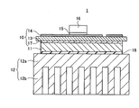
- FIG. 1 is a cross-sectional view showing the structure of a power module according to Embodiment 1 of the present invention.
- FIG. 2 is a flowchart showing a method of manufacturing the power module shown in FIG.
- FIG. 3 is a schematic diagram illustrating a configuration example of a cold spray apparatus.
- FIG. 4 is a table showing characteristics of copper and materials used as additives.
- FIG. 5A is a graph showing experimental results when Invar powder having a center particle diameter of about 25 ⁇ m is used as an additive.
- FIG. 5B is a graph showing experimental results when Invar powder having a center particle size of about 25 ⁇ m is used as an additive.
- FIG. 5C is a graph showing experimental results when Invar powder having a center particle diameter of about 25 ⁇ m is used as an additive.
- FIG. 5A is a graph showing experimental results when Invar powder having a center particle diameter of about 25 ⁇ m is used as an additive.
- FIG. 5B is a graph showing experimental results when Invar
- FIG. 7A is a graph showing experimental results when Invar powder having a center particle diameter of about 11 ⁇ m is used as an additive.
- FIG. 7B is a graph showing experimental results when Invar powder having a center particle diameter of about 11 ⁇ m is used as an additive.
- FIG. 7C is a graph showing experimental results when Invar powder having a center particle diameter of about 11 ⁇ m is used as an additive.
- FIG. 7A is a graph showing experimental results when Invar powder having a center particle diameter of about 11 ⁇ m is used as an additive.
- FIG. 7B is a graph showing experimental results when Invar powder
- FIG. 8A is a graph showing experimental results when Invar powder having a center particle size of about 36 ⁇ m is used as an additive.
- FIG. 8B is a graph showing experimental results when Invar powder having a center particle size of about 36 ⁇ m is used as an additive.
- FIG. 8C is a graph showing experimental results when Invar powder having a center particle size of about 36 ⁇ m is used as an additive.
- FIG. 9A is a graph showing experimental results when tungsten (W) powder is used as an additive.
- FIG. 9B is a graph showing experimental results when tungsten (W) powder is used as an additive.
- FIG. 9C is a graph showing experimental results when tungsten (W) powder is used as an additive.
- FIG. 9A is a graph showing experimental results when tungsten (W) powder is used as an additive.
- FIG. 9B is a graph showing experimental results when tungsten (W) powder is used as an additive.
- FIG. 9C is a graph showing experimental results when tungs
- FIG. 10A is a graph showing experimental results when molybdenum (Mo) powder is used as an additive.
- FIG. 10B is a graph showing experimental results when molybdenum (Mo) powder is used as an additive.
- FIG. 10C is a graph showing experimental results when molybdenum (Mo) powder is used as an additive.
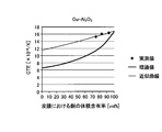
- FIG. 11A is a graph showing experimental results when alumina (Al 2 O 3 ) powder is used as an additive.
- FIG. 11B is a graph showing experimental results when alumina (Al 2 O 3 ) powder is used as an additive.
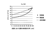
- FIG. 12A is a graph showing experimental results when silicon carbide (SiC) powder is used as an additive.
- SiC silicon carbide
- FIG. 12B is a graph showing experimental results when silicon carbide (SiC) powder is used as an additive.
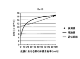
- FIG. 13A is a graph showing experimental results when carbon (C) powder is used as an additive.
- FIG. 13B is a graph showing experimental results when carbon (C) powder is used as an additive.
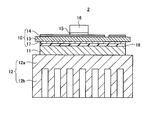
- FIG. 14 is a cross-sectional view showing the structure of the power module according to Embodiment 2 of the present invention.
- FIG. 15 is a flowchart showing a method of manufacturing the power module shown in FIG.
- FIG. 16 is a cross-sectional view showing the structure of a conventional power module.
- FIG. 1 is a cross-sectional view showing the structure of a power module according to Embodiment 1 of the present invention.
- a power module 1 shown in FIG. 1 includes a substrate 10 and a cooler (heat radiator) 12 disposed via the substrate 10 and a buffer layer 11. In such a power module 1, heat generated from the semiconductor chip 16 is transferred to the cooler 12 through the metal layer 17 and the buffer layer 11, and is radiated to the outside.
- the substrate 10 includes a circuit layer 14 formed on one surface of a flat insulating base 13, a semiconductor chip 16 disposed on the circuit layer 14 via solder 15, and the other of the insulating base 13. And a metal layer 17 formed on the surface.
- the insulating base material 13 is an insulating material such as nitride ceramics such as aluminum nitride and silicon nitride, and oxide ceramics such as alumina, magnesia, zirconia, steatite, forsterite, mullite, titania, silica, and sialon. Is a substantially plate-like member.
- the circuit layer 14 is a metal layer made of a metal or alloy having good electrical conductivity such as copper.
- a circuit pattern for transmitting an electrical signal to the semiconductor chip 16 and the like is formed on the circuit layer 14.
- the semiconductor chip 16 is realized by a semiconductor element such as a diode, a transistor, or an insulated gate bipolar transistor (IGBT). A plurality of semiconductor chips 16 may be provided on the circuit layer 14 in accordance with the purpose of use.
- a semiconductor element such as a diode, a transistor, or an insulated gate bipolar transistor (IGBT).
- IGBT insulated gate bipolar transistor
- the metal layer 17 is made of a metal or alloy having good electrical conductivity such as copper, and is provided to transfer heat generated in the semiconductor chip 16 and the circuit layer 14 to the buffer layer 11 and the cooler 12. Yes.
- the buffer layer 11 is made of a composite material in which any of iron nickel alloy (Fe-36Ni, Fe-32Ni-5Co), tungsten, and molybdenum is added to copper, and on the metal layer 17 side of the substrate 10, It is directly formed by a so-called cold spray method.
- the iron-nickel alloy (Fe-36Ni) is generally called Invar (INVAR (registered trademark)), and hereinafter, the iron-nickel alloy (Fe-36Ni) is also referred to as Invar.
- the iron nickel alloy (Fe-32Ni-5Co) is generally called a super invar, and in the following, the iron nickel alloy (Fe-32Ni-5Co) is also called a super invar.
- the buffer layer 11 suppresses the generation of thermal stress due to the high thermal conductivity for efficiently conducting the heat generated in the substrate 10 to the cooler 12 and the difference in thermal expansion coefficient with the insulating base material 13. Therefore, characteristics such as a low coefficient of thermal expansion are required.
- the thermal conductivity ratio of the buffer layer 11 to pure copper is preferably about 50% to 100%.
- the thermal expansion coefficient of the buffer layer 11 is preferably an intermediate value between the thermal expansion coefficient of the substrate 10 on which the semiconductor chip 16 is mounted and the thermal expansion coefficient of the cooler 12.
- the thermal expansion coefficient of the buffer layer 11 is preferably 7.5 ⁇ 10 ⁇ 6 / K or more and less than 16.6 ⁇ 10 ⁇ 6 / K.
- the cold spray method is performed by mixing powders of base materials and additive materials having different specific gravities, Young's moduli, and particle diameters
- the ratio of the additive material in the composite material cannot be increased beyond a certain level. Therefore, in the present application, among the preferable ranges of the thermal expansion coefficient, the range of 13.0 ⁇ 10 ⁇ 6 / K or more and less than 16.6 ⁇ 10 ⁇ 6 / K is targeted, and characteristics within this range are obtained.
- the volume content of the additive with respect to the base material is more than 0% and less than 20%.
- Such a buffer layer 11 is bonded to the cooler 12 via the heat transfer sheet 18 on the surface opposite to the substrate 10 (the lower surface in FIG. 1).
- the cooler 12 is made of a metal or alloy having good thermal conductivity such as aluminum or aluminum alloy, and has a plate-like base portion 12a and a plate shape provided on the back surface (the lower surface in FIG. 1) of the base portion 12a. And a plurality of cooling parts (cooling fins) 12b. The heat generated from the semiconductor chip 16 is released to the outside through the insulating base 13 through the cooler 12.
- the heat transfer sheet 18 is a material in which an adhesive material is disposed on both surfaces of a sheet-like member having good thermal conductivity and electrical insulation.
- the buffer layer 11 and the cooler 12 may be bonded using a gel sheet member or grease instead of the heat transfer sheet 18.
- FIG. 2 is a flowchart showing a method for manufacturing the power module 1.
- step S1 the substrate 10 is manufactured. That is, the circuit layer 14 is formed on one surface of the insulating base 13 and the metal layer 17 is formed on the other surface by a brazing method, and a circuit pattern is formed by an etching method. In addition, you may form the circuit layer 14 and the metal layer 17 using the cold spray method mentioned later instead of the brazing method.
- the semiconductor chip 16 is mounted on the circuit layer 14 using solder 15 or the like.
- a mixed powder as a material for the buffer layer 11 is prepared. That is, a copper powder and an additive powder each having a predetermined center particle diameter are prepared, and both are weighed and mixed so as to have a preset mixing ratio.
- the mixing method of the powder is not particularly limited, and in the first embodiment, mixing is performed by a dry mixing method (dry blending method).
- the particle size of the copper powder is not particularly limited as long as it is a particle size applicable to the cold spray method. Specifically, it may be about 5 to 100 ⁇ m.
- the particle size of the additive powder is preferably within a range of ⁇ 60% with respect to the particle size of the copper powder. This is because it is preferable that the powder of the additive behave similarly to the behavior of the copper powder when the cold spray method is performed. Therefore, for example, when a copper powder having a center particle size of about 25 ⁇ m is used, the center particle size of the additive powder is preferably about 10 to 40 ⁇ m. The method for preparing the powder will be described in detail later.
- FIG. 3 is a schematic diagram illustrating a configuration example of a cold spray apparatus.
- a cold spray device 100 shown in FIG. 3 includes a gas heater 101 that heats compressed gas, a powder supply device 102 that stores powder of a coating material and supplies the powder to the spray gun 103, and a material supplied to the spray gun 103.
- the gas nozzle 104 for injecting the powder together with the heated compressed gas toward the substrate 110, and valves 105 and 106 for adjusting the supply amount of the compressed gas to the gas heater 101 and the powder supply device 102, respectively.
- the compressed gas helium, nitrogen, air or the like is used.
- the compressed gas supplied to the gas heater 101 is heated to a temperature in a range lower than the melting point of the material powder, and then supplied to the spray gun 103.
- the heating temperature of the compressed gas is preferably 300 to 1000 ° C.
- the compressed gas supplied to the powder supply device 102 supplies the material powder in the powder supply device 102 to the spray gun 103 so as to have a predetermined discharge amount.
- the heated compressed gas is injected as a supersonic flow of about 340 m / s or more by passing through a gas nozzle 104 having a divergent shape.
- the gas pressure of the compressed gas is preferably about 1 to 5 MPa. This is because by adjusting the pressure of the compressed gas to this level, the adhesion strength of the coating film 111 to the substrate 110 can be improved. More preferably, the treatment is performed at a pressure of about 2 to 5 MPa.
- the base material 110 As the base material 110, the metal layer 17 side of the substrate 10 is disposed toward the spray gun 103, and the mixed powder prepared in step S2 is charged into the powder supply device 102 and heated by gas. Supply of compressed gas to the vessel 101 and the powder supply device 102 is started. Thereby, the mixed powder supplied to the spray gun 103 is put into the supersonic flow of the compressed gas, accelerated, and sprayed from the spray gun 103. The mixed powder is deposited while colliding with the base material 110, that is, the metal layer 17 of the substrate 10 at a high speed in the solid state, thereby forming the coating film 111. Then, the buffer layer 11 is formed by depositing the film 111 to a desired thickness.
- the film forming apparatus using the cold spray method is limited to the configuration of the cold spray apparatus 100 shown in FIG. 3 as long as it can form a film by colliding the material powder toward the base material 110 in a solid state. Is not to be done.
- step S4 the cooler 12 is attached to the buffer layer 11 formed in step S3 via the heat transfer sheet 18. Thereby, the power module 1 shown in FIG. 1 is completed.
- FIG. 4 is a table showing characteristics of copper as a base material and materials used as an additive.
- the characteristics of silicon nitride used as the base material are shown at the right end of FIG.
- Experiment (1) Mixing ratios of copper powder and additive powder were mixed at various ratios, and a 10 mm film was formed on a 50 mm square ⁇ 3 mm thick aluminum substrate (A1050) by the cold spray method.
- A1050 aluminum substrate
- the copper powder a powder having a center particle diameter of 25 ⁇ m prepared by a water atomization method was used and mixed with the additive powder by a dry mixing method.
- the temperature of the compressed gas was 800 ° C., and the gas pressure was 3 MPa.
- an experiment was performed using three types of powders having a center particle diameter of 11 ⁇ m, 25 ⁇ m, and 36 ⁇ m.
- the volume content of copper in the formed film was measured, and the correlation between the volume content of copper in the mixed powder and the volume content of copper in the film was determined.
- the volume content of copper in the film was calculated by performing image analysis on the SEM image of the film surface and comparing the area of the copper region with the area of the additive material region.
- Experiment (2) A 10 mm thick film was formed in the same manner as in Experiment (1), and a 2 mm square ⁇ 40 mm thick test piece was cut out from the film by the discharge wire method, and the conductivity was measured by the four-terminal method. From the measurement results, the correlation between the copper volume content and the electrical conductivity in the coating was determined.
- Experiment (3) A 10 mm thick film was formed in the same manner as in Experiment (1), and a 2 mm square x 15 mm thick test piece was cut out from the film by the discharge wire method, and heat in a direction perpendicular to the film deposition direction The expansion coefficient was measured. From the measurement results, the correlation between the volume content of copper in the coating and the coefficient of thermal expansion was determined.
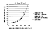
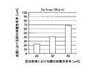
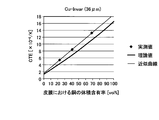
- FIGS. 5A to 5C are graphs respectively showing the results of experiments (1) to (3) in the case of using Invar powder having a center particle size of about 25 ⁇ m as an additive.
- the horizontal axis of FIG. 5A shows the volume content [vol%] of copper in the mixed powder before film formation
- the vertical axis shows the volume content [vol%] of copper in the film after film formation. .
- FIG. 5B shows the horizontal axis of FIG. 5B shows the volume content [vol%] of the copper in a film
- thermal conductivity ratio is evaluated by electrical conductivity ratio.
- FIG. 5B also shows the theoretical value of the thermal conductivity ratio with respect to the copper volume content. This theoretical value is calculated by the following equation (1).
- FIG. 5C shows the horizontal axis of FIG. 5C shows the volume content [vol%] of copper in the film, and the vertical axis shows the coefficient of thermal expansion (CTE) [ ⁇ 10 ⁇ 6 / K].
- ⁇ c coefficient of thermal expansion in the composite material
- v m volume content of the base material (copper)
- v a Volume content of additive material
- E a Young's modulus of additive material
- ⁇ a Thermal expansion coefficient of additive material In the case of Invar, Young's modulus E a of the additive material is 142 GPa, and thermal expansion coefficient ⁇ a of the additive material Is 1.2 ⁇ 10 ⁇ 6 / K.
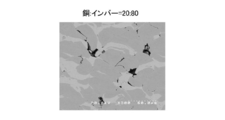
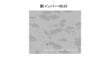
- FIGS. 6A to 6C are SEM images showing the surface of the film obtained by the experiment (1).
- FIG. 6A shows the case where the mixing ratio (copper: invar) of copper and invar in the mixed powder is 20:80
- FIG. 6B is 50:50
- FIG. 6C is 80:20.
- the volume content of copper in the mixed powder before film formation is generally linearly related to the volume content of copper in the film. It was observed. From this, it is understood that the ratio of copper and invar contained in the coating can be controlled with high accuracy by adjusting the mixing ratio of copper and invar in the powder state.
- the measured value of the electrical conductivity ratio with respect to the volume content of copper tended to be almost in line with the theoretical value of the thermal conductivity ratio. From this, it can be seen that the conductivity ratio (thermal conductivity ratio) of the coating can be controlled by adjusting the ratio of copper and invar contained in the coating. Specifically, the conductivity ratio can be 50% or more suitable for the buffer layer 11 by setting the volume content of copper to about 75% or more, that is, the volume content of Invar is less than about 25%. .
- the measured value of the coefficient of thermal expansion with respect to the volume content of copper tended to be almost in line with the theoretical value.
- the coefficient of thermal expansion can be controlled by adjusting the ratio of copper and invar in the coating. Specifically, by setting the volume content of copper to about 80% or more, that is, the volume content of Invar is less than about 20%, the coefficient of thermal expansion is 13.0 ⁇ 10 ⁇ 6 / suitable for the buffer layer 11. K or more and less than 16.6 ⁇ 10 ⁇ 6 / K.
- the volume content of copper in the film is about 80% or more, that is, the volume content of Invar is less than about 20%. Just do it.
- the volume content of copper in the mixed powder is about 90% or more, that is, The volume content of invar may be less than about 10%.
- FIGS. 7A to 7C are graphs respectively showing the results of experiments (1) to (3) in the case of using Invar powder having a center particle diameter of about 11 ⁇ m as an additive.
- FIG. 7A when the center particle diameter of the Invar powder is 11 ⁇ m, there is a substantially linear relationship between the copper volume content in the mixed powder before film formation and the copper volume content in the film. It was observed. This shows that the ratio of copper and invar contained in the coating can be controlled with high accuracy by adjusting the mixing ratio of copper and invar in the powder state.
- the measured value of the conductivity ratio with respect to the volume content of copper tended to be almost in line with the theoretical value of the thermal conductivity ratio.
- the measured value of the thermal expansion coefficient with respect to the volume content of copper showed the tendency which followed the theoretical value in general. Therefore, even when the center particle diameter of invar is 11 ⁇ m, it can be seen that the conductivity ratio and thermal expansion coefficient of the film can be controlled by adjusting the ratio of copper to invar in the film.
- the volume content of copper in the mixed powder is about 90% or more, that is, The volume content of invar may be less than about 10%.
- FIG. 8A to 8C are graphs showing the results of experiments (1) to (3), respectively, in the case where Invar powder having a center particle diameter of about 36 ⁇ m was used as an additive.
- FIG. 8A when the center particle diameter of the Invar powder is 36 ⁇ m, there is a substantially linear relationship between the copper volume content in the mixed powder before film formation and the copper volume content in the film. It was observed. This shows that the ratio of copper and invar contained in the coating can be controlled with high accuracy by adjusting the mixing ratio of copper and invar in the powder state.
- the measured value of the conductivity ratio with respect to the volume content of copper tended to be almost in line with the theoretical value of the thermal conductivity ratio.
- the measured value of the coefficient of thermal expansion with respect to the volume content of copper tended to be almost in line with the theoretical value. Therefore, even when the center particle diameter of Invar is set to 36 ⁇ m, it can be seen that the conductivity ratio and the thermal expansion coefficient of the film can be controlled by adjusting the ratio of copper to Invar in the film.
- the volume content of copper in the mixed powder is about 90% or more, that is, The volume content of invar may be less than about 10%.
- FIGS. 9A to 9C are graphs respectively showing the results of experiments (1) to (3) in the case of using tungsten (W) powder having a center particle size of about 9.8 ⁇ m as an additive.
- the theoretical value shown in FIG. 9B is calculated by assuming that the thermal conductivity ⁇ a of the additive is 174 W / m ⁇ K in the equation (1).
- the theoretical values shown in FIG. 9C are calculated in Formula (2) with the Young's modulus E a of the additive as 400 GPa and the thermal expansion coefficient ⁇ a of the additive as 4.5 ⁇ 10 ⁇ 6 / K. is there.
- the volume content of copper in the coating was larger than the volume content of copper in the mixed powder. This indicates that when a film is formed by the cold spray method, it is difficult to increase the volume content of tungsten to a level of, for example, about 30% or more because tungsten powder hardly enters the film. .
- copper is about 70% or more, that is, when tungsten is in the range of less than about 30%, there is a substantially linear relationship between the volume content of copper in the mixed powder and the volume content of copper in the coating. Therefore, it is possible to control the ratio of copper and tungsten in the coating by adjusting the mixing ratio of copper and tungsten in the powder state.
- the measured value of the conductivity ratio with respect to the volume content of copper deviated from the theoretical value of the thermal conductivity ratio.
- the conductivity ratio can be 50% or more suitable for the buffer layer 11 by setting the volume content of copper to about 75% or more, that is, the volume content of tungsten is less than about 25%. .
- the coefficient of thermal expansion can be controlled by adjusting the ratio of copper and tungsten in the coating. For example, when the volume content of copper is about 85% or more, that is, the volume content of tungsten is less than about 15%, the coefficient of thermal expansion is 13.0 ⁇ 10 ⁇ 6 / K or more suitable for the buffer layer 16 16 Less than 6 ⁇ 10 ⁇ 6 / K.
- a film having a thermal conductivity and a thermal expansion coefficient suitable for the buffer layer 11 specifically, a film having a copper volume content of 85% or more is obtained by the cold spray method.
- the volume content of copper in the mixed powder may be about 60% or more, that is, the volume content of tungsten may be less than about 40%.
- FIGS. 10A to 10C are graphs showing the results of experiments (1) to (3), respectively, when molybdenum (Mo) powder having a center particle size of about 5.3 ⁇ m is used as an additive.
- Mo molybdenum
- FIG. 10B is calculated by assuming that the thermal conductivity ⁇ a of the additive is 138 W / m ⁇ K in the equation (1).
- FIG. 10C are calculated in Formula (2) with Young's modulus E a of the additive as 330 GPa and thermal expansion coefficient ⁇ a of the additive as 4.8 ⁇ 10 ⁇ 6 / K. is there.
- the volume content of copper in the coating was larger than the volume content of copper in the mixed powder. This indicates that when a film is formed by the cold spray method, it is difficult to increase the volume content of molybdenum to a level of, for example, 35% or more because molybdenum powder hardly enters the film. However, if the copper content is 65% or more, that is, the molybdenum content is less than 35%, a predetermined tendency is observed between the copper volume content in the mixed powder and the copper volume content in the coating. It is possible to control the ratio of copper and molybdenum in the coating by adjusting the mixing ratio of copper and molybdenum in the above state.
- the measured value of the conductivity ratio with respect to the volume content of copper deviated from the theoretical value of the thermal conductivity ratio.
- the conductivity ratio with respect to the volume content of copper there is a certain relationship in the conductivity ratio with respect to the volume content of copper, so it is possible to control the conductivity ratio of the film by adjusting the ratio of copper and molybdenum. is there.
- the conductivity ratio can be 50% or more suitable for the buffer layer 11 regardless of the volume content of copper.
- the volume content of molybdenum in the coating is about 35% or more, that is, the volume of molybdenum.
- the coefficient of thermal expansion can be controlled by adjusting the ratio of copper and molybdenum in the coating. For example, when the volume content of copper is about 85% or more (molybdenum is less than about 15%), the coefficient of thermal expansion is 13.0 ⁇ 10 ⁇ 6 / K or more suitable for the buffer layer 11 and 16.6 ⁇ 10. -6 / K or less.
- a film having a thermal conductivity and a coefficient of thermal expansion suitable for the buffer layer 11 is obtained by the cold spray method.
- the volume content of copper in the mixed powder may be about 65% or more, that is, the volume content of molybdenum may be less than about 35%.
- FIGS. 11A and 11B are graphs showing the results of experiments (1) and (3), respectively, when an alumina (Al 2 O 3 ) powder having a center particle size of about 30 ⁇ m is used as an additive.
- the theoretical values shown in FIG. 11B are calculated by assuming that the Young's modulus E a of the additive is 380 GPa and the thermal expansion coefficient ⁇ a of the additive is 7.2 ⁇ 10 ⁇ 6 / K in the formula (2). It is.
- the conductivity ratio thermal conductivity ratio
- the conductivity ratio is not evaluated because the conductivity ratio of the film to pure copper does not correspond to the thermal conductivity ratio to pure copper.
- the volume content of copper in the film was larger than the volume content of copper in the mixed powder. This indicates that when a film is formed by the cold spray method, the alumina powder hardly enters the film. Therefore, it can be said that it is difficult to increase the volume content of alumina in the coating to a level of, for example, 30% or more, or to control the ratio of both in the coating by the mixing ratio of copper and alumina in the mixed powder.
- FIG. 12A and 12B are graphs showing the results of experiments (1) and (3), respectively, when silicon carbide (SiC) powder having a center particle size of about 30 ⁇ m is used as an additive.
- SiC silicon carbide
- FIG. 12B the theoretical values shown in FIG. 12B are calculated by assuming that the Young's modulus E a of the additive is 450 GPa and the thermal expansion coefficient ⁇ a of the additive is 4.4 ⁇ 10 ⁇ 6 / K in the formula (2). It is.
- the volume content of copper in the coating was larger than the volume content of copper in the mixed powder. This indicates that when a film is formed by the cold spray method, the silicon carbide powder hardly enters the film. Therefore, it is difficult to increase the volume content of silicon carbide in the coating to a level of, for example, 20% or more, or to control the ratio of both in the coating by the mixing ratio of copper and silicon carbide in the mixed powder.
- 13A and 13B are graphs showing the results of experiments (1) and (3), respectively, in the case of using carbon (C) powder having a center particle size of about 25 ⁇ m as an additive.
- the theoretical values shown in FIG. 13B are calculated by assuming that the Young's modulus E a of the additive is 15 GPa and the thermal expansion coefficient ⁇ a of the additive is 4.4 ⁇ 10 ⁇ 6 / K in the formula (2). It is.
- the volume content of copper in the coating was greater than the volume content of copper in the mixed powder. This indicates that when a film is formed by the cold spray method, the carbon powder hardly enters the film. Therefore, it is difficult to increase the volume content of carbon to a level of, for example, 10% or more in the film, or to control the ratio of both in the film by the mixing ratio of copper and carbon in the mixed powder.
- an iron nickel alloy, tungsten, or molybdenum is used as the additive, and the volume of the additive in the film.
- the content is preferably less than 20%.
- the volume content of the additive in the coating is preferably less than 15%.
- the buffer layer 11 can be directly formed on the metal layer 17 of the substrate 10 by using the cold spray method. Therefore, the thermal stress between the insulating base material 13 and the cooler 12 can be relaxed. Further, one heat resistance layer such as a heat transfer sheet or grease can be omitted from the configuration of the conventional power module. Accordingly, it is possible to realize a power module that can efficiently release the heat generated in the substrate 10 and has excellent durability.
- the mixed powder of copper and an additive made of iron-nickel alloy, tungsten, or molybdenum is applied to the material powder of the cold spray method, so that the powder mixing ratio is adjusted.
- a film having a desired composition ratio in other words, a film having a desired coefficient of thermal expansion and thermal conductivity can be easily formed.
- the thermal expansion coefficient and thermal conductivity of the film can be easily controlled by adjusting the mixing ratio of the copper and additive powders. Therefore, a film corresponding to required characteristics such as low thermal expansion and high thermal conductivity can be easily realized like the buffer layer 11 in the power module 1.
- the control of the composition and characteristics of such a film can be performed more easily and at a lower cost than in the case of a sintered body.
- FIG. 14 is a cross-sectional view showing the structure of the power module according to the second embodiment.
- a buffer layer 11 is formed directly on the surface of the cooler 12 (upper surface in FIG. 14) as compared with the power module 1 shown in FIG. The difference is that the buffer layer 11 is bonded to the metal layer 17 side of the substrate 10.
- the material and configuration of each part are the same as in the first embodiment.
- FIG. 15 is a flowchart showing a method for manufacturing the power module 2. Among these, steps S1 and S2 are the same as those in the first embodiment.
- step S5 following step S2 the buffer layer 11 is formed on the cooler 12 by a cold spray method. That is, in the cold spray device 100 illustrated in FIG. 3, the surface of the base 12 a of the cooler 12 (upper surface in FIG. 14) is disposed as the base material 110 toward the spray gun 103, and the mixed powder prepared in step S ⁇ b> 2. Is put into the powder supply apparatus 102 to form a film.
- step S6 the substrate 10 produced in step S1 is attached to the buffer layer 11 formed in step S5 via the heat transfer sheet 18. Thereby, the power module 2 shown in FIG. 14 is completed.
- the buffer layer 11 is formed directly on the cooler 12 side, one heat resistance layer such as a heat transfer sheet or grease can be omitted from the configuration of the conventional power module. Therefore, it is possible to efficiently release the heat generated in the substrate 10 and realize a power module excellent in durability.
Landscapes
- Chemical & Material Sciences (AREA)
- Chemical Kinetics & Catalysis (AREA)
- Engineering & Computer Science (AREA)
- Materials Engineering (AREA)
- Mechanical Engineering (AREA)
- Metallurgy (AREA)
- Organic Chemistry (AREA)
- Cooling Or The Like Of Semiconductors Or Solid State Devices (AREA)
- Other Surface Treatments For Metallic Materials (AREA)
Abstract
パワーモジュールの緩衝層として必要な性能を有し、低コストで作製可能な複合材、該複合材を含む積層体、及び、熱伝導効率の低下を抑制しつつ基板と冷却器との間の熱応力を緩和することができるパワーモジュールを提供する。パワーモジュール1は、一方の面に半導体チップ16が実装された基板10と、該基板10の他方の面に形成された緩衝層11と、平板状をなす基部12aと該基部12aの一方の面に設けられた冷却部12bを有し、基部12aの他方の面において緩衝層11と接着された冷却器12とを備える。緩衝層11は、銅の粉末と、鉄ニッケル合金、タングステン、及びモリブデンのいずれかからなる添加材の粉末とを混合した混合粉末をガスと共に加速し、基材の表面に固相状態のままで吹き付けて堆積させることによって形成され、上記添加材の体積含有率が0%より大きく20%未満の複合材である。
Description
本発明は、複数種類の金属からなる複合材、該複合材を含む積層体、及び該複合材が適用されたパワーモジュールに関する。
従来、産業用、自動車用などの電力制御からモータ制御まで、幅広い分野に使用される省エネルギー化のキーデバイスとして、パワーモジュールが知られている。図16は、従来のパワーモジュールを模式的に示す断面図である。図16に示すように、パワーモジュール9は、セラミックス等からなる絶縁基材91の一方の面に回路層92及び半田93を介して半導体チップ94を配設し、他方の面に金属層95を形成した基板96を、金属板からなる緩衝層97を介して冷却器(放熱器)98を配設した装置である。このようなパワーモジュール9においては、半導体チップ94から発生した熱を、金属層95及び緩衝層97を介して冷却器98に移動させて外部に放熱することにより、冷却を行うことができる。
緩衝層97は、絶縁基材91と冷却器98との間の熱応力を緩和するために配設されている。このため、緩衝層97の材料としては通常、低膨張性及び高熱伝導性の金属、具体的には銅タングステンや銅モリブデンなどの複合材料が用いられる。また、特許文献1には、第1の材料としての銅(Cu)と、該第1の材料よりも熱膨張係数の小さい第2の材料としてのケイ素(Si)、アルミナ(Al2O3)、炭化ケイ素(SiC)、窒化ケイ素(Si3N4)、二酸化ケイ素(SiO2)、窒化アルミニウム(AlN)、タングステン(W)、モリブデン(Mo)、インバー合金等とを含み、コールドスプレー法により形成された下敷き導電部材を、金属配線と半導体チップとの間に設けたパワーモジュールが開示されている。
コールドスプレー法とは、材料の粉末を、融点又は軟化点以下の状態の不活性ガスと共に末広ノズル(ラバルノズル)から噴射し、固相状態のまま基材に衝突させることにより、基材の表面に皮膜を形成する方法である。コールドスプレー法においては、溶射法と比較して低い温度で加工が行われるので、熱応力の影響が緩和される。そのため、相変態がなく酸化も抑制された金属皮膜を得ることができる。特に、基材及び皮膜となる材料が共に金属である場合、金属材料の粉末が基材、又は先に形成された皮膜に衝突した際に粉末と基材との間で塑性変形が生じてアンカー効果が得られると共に、互いの酸化皮膜が破壊されて新生面同士による金属結合が生じるので、密着強度の高い積層体を得ることができる。
例えば非特許文献1には、銅とタングステンの複合材をコールドスプレー法により形成する技術が開示されている。また、非特許文献2には、パワーモジュールの一部をコールドスプレー法により形成する技術が開示されている。
カン(Hyun-Ki Kang)、他、「Tungsten/Copper composite deposite produced by a cold spray」、スクリプタ マテリアリア(Scripta Materialia)49(2003年)、第1169~1174頁
オスターヴァルト(Osterwald)、他、「Sprayed Stress Reducing Interlayers for Highly Reliable Large Solder Joints」、[2013年12月11日検索]、インターネット<http://www.danfoss.com/NR/rdonlyres/522FBBBC-EA80-4CEE-8BCC-361026167619/0/InterlayersforHighlyReliableLargeSolderJoints_PCIM2007.pdf>
図16に示すパワーモジュール9において、緩衝層97は、伝熱シートやグリス99を用いて基板96及び冷却器98に接着されているため、伝熱シートやグリス99がモジュールの熱抵抗を増大させる要因になっていた。そのため、熱抵抗の増大を抑制しつつ、基板と冷却器との間の熱応力を緩和することができるパワーモジュールの構造の開発が望まれていた。また、緩衝層97の材料として用いられる銅タングステンなどの複合材料は高価であるため、パワーモジュール9のサイズが大きくなるとコストが大幅に上昇してしまう。そのため、パワーモジュールに適用することができ、低熱膨張性及び高熱伝導性といった用途に応じて必要な性能を維持しつつ、コストを低減することができる緩衝層の材料の開発も望まれている。
この点について、特許文献1においては下敷き導電部材による熱応力の緩和作用にしか着目しておらず、熱応力の緩和と熱抵抗の抑制とを両立可能な材料は従来知られていない。
本発明は、上記に鑑みてなされたものであって、パワーモジュールの緩衝層として必要な性能を有し、低コストで作製可能な複合材、該複合材を含む積層体、及び、熱伝導効率の低下を抑制しつつ基板と冷却器との間の熱応力を緩和することができるパワーモジュールを提供することを目的とする。
上述した課題を解決し、目的を達成するために、本発明に係る複合材は、銅の粉末と、鉄ニッケル合金、タングステン、及びモリブデンのいずれかからなる添加材の粉末とを混合した混合粉末をガスと共に加速し、基材の表面に固相状態のままで吹き付けて堆積させることによって形成され、前記添加材の体積含有率が0%より大きく20%未満であることを特徴とする。
上記複合材において、前記鉄ニッケル合金は、Fe-36Ni又はFe-32Ni-5Coであることを特徴とする。
本発明に係る積層体は、前記複合材と、前記基材と、を備えることを特徴とする。
本発明に係るパワーモジュールは、一方の面に半導体素子が実装された基板と、前記基板の他方の面を前記基材の表面として形成された前記複合材と、平板状をなす基部と、該基部の一方の面に設けられた冷却部と、を有し、前記基部の他方の面において前記複合材と接着された冷却器と、を備えることを特徴とする。
本発明に係るパワーモジュールは、平板状をなす基部と、該基部の一方の面に設けられた冷却部と、を有する冷却器と、前記基部の他方の面を前記基材の表面として形成された前記複合材と、一方の面に半導体素子が実装され、他方の面において前記複合材に接着された基板と、を備えることを特徴とする。
本発明によれば、銅に、鉄ニッケル合金、タングステン、及びモリブデンのいずれかの金属が添加された複合材を所謂コールドスプレー法によって形成するので、パワーモジュールの緩衝層として必要な性能を有する複合材を低コストで作製することができる。また、本発明によれば、そのような複合材を所謂コールドスプレー法によりパワーモジュールの基板と冷却器のいずれかに直接形成するので、熱伝導効率の低下を抑制しつつ、基板と冷却器との間の熱応力を緩和することが可能となる。
以下、本発明を実施するための形態を、図面を参照しながら詳細に説明する。なお、以下の実施の形態により本発明が限定されるものではない。また、以下の説明において参照する各図は、本発明の内容を理解し得る程度に形状、大きさ、及び位置関係を概略的に示してあるに過ぎない。即ち、本発明は各図で例示された形状、大きさ、及び位置関係のみに限定されるものではない。
(実施の形態1)
図1は、本発明の実施の形態1に係るパワーモジュールの構造を示す断面図である。図1に示すパワーモジュール1は、基板10と、該基板10と緩衝層11を介して配設された冷却器(放熱器)12とを備える。このようなパワーモジュール1においては、半導体チップ16から発生した熱を、金属層17及び緩衝層11を介して冷却器12に移動させることにより、外部に放熱する。
図1は、本発明の実施の形態1に係るパワーモジュールの構造を示す断面図である。図1に示すパワーモジュール1は、基板10と、該基板10と緩衝層11を介して配設された冷却器(放熱器)12とを備える。このようなパワーモジュール1においては、半導体チップ16から発生した熱を、金属層17及び緩衝層11を介して冷却器12に移動させることにより、外部に放熱する。
基板10は、平板状をなす絶縁基材13の一方の面に形成された回路層14と、該回路層14に半田15を介して配設された半導体チップ16と、絶縁基材13の他方の面に形成された金属層17とを有する。
絶縁基材13は、例えば、窒化アルミニウム、窒化ケイ素等の窒化物系セラミックスや、アルミナ、マグネシア、ジルコニア、ステアタイト、フォルステライト、ムライト、チタニア、シリカ、サイアロン等の酸化物系セラミックスといった絶縁性材料からなる略板状の部材である。
回路層14は、例えば銅等の良好な電気伝導度を有する金属又は合金からなる金属層である。この回路層14には、半導体チップ16等に対して電気信号を伝達するための回路パターンが形成されている。
半導体チップ16は、ダイオード、トランジスタ、絶縁ゲートバイポーラトランジスタ(IGBT)等の半導体素子によって実現される。なお、半導体チップ16は、使用の目的に合わせて回路層14上に複数個設けられても良い。
金属層17は、例えば銅等の良好な電気伝導度を有する金属又は合金からなり、半導体チップ16及び回路層14において発生した熱を緩衝層11及び冷却器12に伝熱するために設けられている。
緩衝層11は、銅に対し、鉄ニッケル合金(Fe-36Ni、Fe-32Ni-5Co)と、タングステンと、モリブデンとのいずれかを添加した複合材からなり、基板10の金属層17側に、所謂コールドスプレー法により直接形成されている。なお、鉄ニッケル合金(Fe-36Ni)は一般にインバー(INVAR(登録商標))と呼ばれており、以下においても、鉄ニッケル合金(Fe-36Ni)のことをインバーともいう。また、鉄ニッケル合金(Fe-32Ni-5Co)は一般にスーパーインバーと呼ばれており、以下においても、鉄ニッケル合金(Fe-32Ni-5Co)のことをスーパーインバーともいう。
緩衝層11には、基板10において発生した熱を効率良く冷却器12に伝導させるための高熱伝導率、及び、絶縁基材13との熱膨張率の差に起因する熱応力の発生を抑制するための低熱膨張率といった特性が要求される。具体的には、純銅に対する緩衝層11の熱伝導率比が50%~100%程度であることが好ましい。また、緩衝層11の熱膨張率は、半導体チップ16が実装される基板10の熱膨張率と冷却器12の熱膨張率との中間的な値であることが好ましい。例えば、基板10の熱膨張率が4.0~7.5×10⁻⁶/K程度であり、冷却器12が熱膨張率23.6×10-6/Kのアルミニウムで形成されている場合、緩衝層11の熱膨張率を7.5×10-6/K以上16.6×10-6/K未満にすると良い。
しかしながら、比重やヤング率や粒径が互いに異なる母材及び添加材の粉末を混合してコールドスプレー法を行う場合、複合材における添加材の比率を一定以上に上げられないなどの事情がある。そのため、本出願においては、上記熱膨張率の好ましい範囲のうち、13.0×10⁻⁶/K以上16.6×10-6/K未満の範囲を目標とし、この範囲の特性を得るために、母材に対する添加材の体積含有率を0%より多く20%未満としている。
このような緩衝層11は、基板10と反対側の面(図1においては下面)において、伝熱シート18を介して冷却器12と接着されている。冷却器12は、アルミニウムやアルミニウム合金等の良好な熱伝導性を有する金属又は合金からなり、平板状をなす基部12aと、該基部12aの裏面(図1においては下面)に設けられた板状をなす複数の冷却部(冷却フィン)12bとを有する。このような冷却器12を介して、半導体チップ16から発生した熱が絶縁基材13を介して外部に放出される。
伝熱シート18は、良好な熱伝導性及び電気絶縁性を有するシート状部材の両面に粘着材を配置した材料である。なお、伝熱シート18の代わりに、ゲル状のシート部材やグリスを用いて緩衝層11と冷却器12とを接着しても良い。
次に、パワーモジュール1の製造方法について説明する。図2は、パワーモジュール1の製造方法を示すフローチャートである。
まず、工程S1において、基板10を作製する。即ち、絶縁基材13の一方の面に回路層14を、他方の面に金属層17をろう付法により形成し、エッチング法により回路パターンを形成する。なお、ろう付法の代わりに、後述するコールドスプレー法を用いて回路層14や金属層17を形成しても良い。半導体チップ16は半田15等を用いて回路層14上に実装される。
続く工程S2において、緩衝層11の材料となる混合粉末を調製する。即ち、所定の中心粒径をそれぞれ有する銅の粉末及び添加材の粉末を用意し、予め設定された混合比率となるように両者を秤量して混合する。粉末の混合方法は特に限定されず、本実施の形態1においては、乾式混合法(ドライブレンド法)によって混合する。
銅の粉末の粒径については、コールドスプレー法に適用可能な粒径であれば特に限定されない。具体的には、5~100μm程度であれば良い。一方、添加材の粉末の粒径は、銅の粉末の粒径に対して±60%の範囲内にすると良い。これは、コールドスプレー法を行った際に、銅の粉末のふるまいに対して添加材の粉末が同様にふるまうことが好ましいからである。そのため、例えば、中心粒径が約25μmの銅の粉末を用いる場合、添加材の粉末の中心粒径を10~40μm程度にすると良い。粉末の調製方法については、後で詳しく説明する。
続く工程S3において、コールドスプレー法により、工程S1において作製した基板10の金属層17側に緩衝層11を形成する。図3は、コールドスプレー装置の構成例を示す模式図である。図3に示すコールドスプレー装置100は、圧縮ガスを加熱するガス加熱器101と、皮膜の材料の粉末を収容してスプレーガン103に供給する粉末供給装置102と、スプレーガン103に供給された材料の粉末を、加熱された圧縮ガスと共に基材110に向けて噴射するガスノズル104と、ガス加熱器101及び粉末供給装置102に対する圧縮ガスの供給量をそれぞれ調節するバルブ105及び106とを備える。
圧縮ガスとしては、ヘリウム、窒素、空気などが使用される。ガス加熱器101に供給された圧縮ガスは、材料の粉末の融点よりも低い範囲の温度に加熱された後、スプレーガン103に供給される。圧縮ガスの加熱温度は、好ましくは300~1000℃である。
一方、粉末供給装置102に供給された圧縮ガスは、粉末供給装置102内の材料粉末をスプレーガン103に所定の吐出量となるように供給する。
加熱された圧縮ガスは、末広形状をなすガスノズル104を通過することにより、約340m/s以上の超音速流となって噴射される。この際の圧縮ガスのガス圧力は、1~5MPa程度とすることが好ましい。圧縮ガスの圧力をこの程度に調整することにより、基材110に対する皮膜111の密着強度の向上を図ることができるからである。より好ましくは、2~5MPa程度の圧力で処理すると良い。
このようなコールドスプレー装置100において、基材110として、基板10の金属層17側をスプレーガン103に向けて配置すると共に、工程S2において調製した混合粉末を粉末供給装置102に投入し、ガス加熱器101及び粉末供給装置102への圧縮ガスの供給を開始する。それにより、スプレーガン103に供給された混合粉末が、この圧縮ガスの超音速流の中に投入されて加速され、スプレーガン103から噴射される。この混合粉末が、固相状態のまま基材110、即ち基板10の金属層17に高速で衝突して堆積することにより、皮膜111が形成される。そして、この皮膜111を所望の厚さとなるまで堆積させることで、緩衝層11が形成される。
なお、コールドスプレー法による成膜装置としては、材料の粉末を基材110に向けて固相状態で衝突させて皮膜を形成できる装置であれば、図3に示すコールドスプレー装置100の構成に限定されるものではない。
続く工程S4において、伝熱シート18を介して、工程S3において形成した緩衝層11に冷却器12を貼り付ける。それにより、図1に示すパワーモジュール1が完成する。
次に、工程S2における混合粉末の調製方法を詳しく説明する。本願発明者は、緩衝層11として好適な高熱伝導率及び低熱膨張率を有し、且つ、容易に作製することができる複合材を探索するため、銅に対して種々の材料を添加した混合粉末を用いてコールドスプレー法により皮膜を形成する実験を実施した。図4は、母材である銅及び添加材として用いた材料の特性を示す表である。併せて、図4の右端に、基材(図1に示す絶縁基材13)として用いられる窒化ケイ素の特性を示す。
具体的には、以下の実験(1)~(3)を行った。
実験(1):銅の粉末と添加材の粉末との混合比率を種々の比率で混合し、コールドスプレー法により、50mm角×3mm厚のアルミニウム基材(A1050)上に10mmの皮膜を形成した。銅の粉末としては、水アトマイズ法で作製した中心粒径25μmの粉末を用い、乾式混合法により添加材の粉末と混合した。銅の粉末と添加材の粉末との混合比率は、銅:添加材=20:80、50:50、及び80:20の3種類とした。また、コールドスプレー条件としては、圧縮ガスの温度を800℃とし、ガス圧力を3MPaとした。なお、インバーについては、中心粒径が11μm、25μm、及び36μmの3種類の粉末を用いて実験を行った。
実験(1):銅の粉末と添加材の粉末との混合比率を種々の比率で混合し、コールドスプレー法により、50mm角×3mm厚のアルミニウム基材(A1050)上に10mmの皮膜を形成した。銅の粉末としては、水アトマイズ法で作製した中心粒径25μmの粉末を用い、乾式混合法により添加材の粉末と混合した。銅の粉末と添加材の粉末との混合比率は、銅:添加材=20:80、50:50、及び80:20の3種類とした。また、コールドスプレー条件としては、圧縮ガスの温度を800℃とし、ガス圧力を3MPaとした。なお、インバーについては、中心粒径が11μm、25μm、及び36μmの3種類の粉末を用いて実験を行った。
そして、形成した皮膜における銅の体積含有率を測定し、混合粉末における銅の体積含有率と、皮膜における銅の体積含有率との相関を求めた。皮膜における銅の体積含有率は、皮膜表面のSEM画像に対して画像解析を行い、銅の領域の面積と添加材の領域の面積とを比較することにより算出した。
実験(2):実験(1)と同様にして厚さ10mmの皮膜を形成し、この皮膜から2mm角×40mm厚の試験片を放電ワイヤー法により切り出し、四端子法により導電率を測定した。該測定結果より、皮膜における銅の体積含有率と導電率との相関を求めた。
実験(3):実験(1)と同様にして厚さ10mmの皮膜を形成し、この皮膜から2mm角×15mm厚の試験片を放電ワイヤー法により切り出し、皮膜の堆積方向と直交する方向における熱膨張率を測定した。該測定結果より、皮膜における銅の体積含有率と熱膨張率との相関を求めた。
図5A~図5Cは、中心粒径が約25μmのインバーの粉末を添加材として用いた場合の実験(1)~(3)の結果をそれぞれ示すグラフである。このうち、図5Aの横軸は、成膜前の混合粉末における銅の体積含有率[vol%]を示し、縦軸は、成膜後の皮膜における銅の体積含有率[vol%]を示す。
また、図5Bの横軸は、皮膜における銅の体積含有率[vol%]を示し、縦軸は、純銅に対する導電率比[%]を示す。ここで、純銅に対する導電率比は、純銅に対する熱伝導率比に対応するため、以下においては、導電率比により熱伝導率比を評価する。図5Bには併せて、銅の体積含有率に対する熱伝導率比の理論値も表示している。この理論値は、次式(1)により算出されたものである。

式(1)における各符号は、以下の値を示す。
1-Φ:複合材における添加材の体積含有率
λc:複合材における熱伝導率
λm:母材(銅)の熱伝導率(銅の場合、λm=397W/m・K)
λa:添加材の熱伝導率
インバーの場合、添加材の熱伝導率λaは13.4W/m・Kである。
1-Φ:複合材における添加材の体積含有率
λc:複合材における熱伝導率
λm:母材(銅)の熱伝導率(銅の場合、λm=397W/m・K)
λa:添加材の熱伝導率
インバーの場合、添加材の熱伝導率λaは13.4W/m・Kである。
また、図5Cの横軸は、皮膜における銅の体積含有率[vol%]を示し、縦軸は、熱膨張率(CTE)[×10-6/K]を示す。図5Cには併せて、銅の体積含有率に対する熱膨張率の理論値も表示している。この理論値は、次式(2)によって与えられるターナー(Turner)則に従って算出されたものである。
αc=(vmEmαm+vaEaαa)/(vmEm+vaEa) …(2)
αc=(vmEmαm+vaEaαa)/(vmEm+vaEa) …(2)
式(2)における各符号は、以下の値を示す。
αc:複合材における熱膨張率
vm:母材(銅)の体積含有率
Em:母材のヤング率(銅の場合、Em=120GPa)
αm:母材の熱膨張率(銅の場合、αm=16.6×10⁻⁶/K)
va:添加材の体積含有率
Ea:添加材のヤング率
αa:添加材の熱膨張率
インバーの場合、添加材のヤング率Eaは142GPaであり、添加材の熱膨張率αaは1.2×10⁻⁶/Kである。
αc:複合材における熱膨張率
vm:母材(銅)の体積含有率
Em:母材のヤング率(銅の場合、Em=120GPa)
αm:母材の熱膨張率(銅の場合、αm=16.6×10⁻⁶/K)
va:添加材の体積含有率
Ea:添加材のヤング率
αa:添加材の熱膨張率
インバーの場合、添加材のヤング率Eaは142GPaであり、添加材の熱膨張率αaは1.2×10⁻⁶/Kである。
また、図6A~図6Cは、実験(1)により得られた皮膜の表面を写したSEM画像である。このうち、図6Aは混合粉末における銅とインバーとの混合比率(銅:インバー)が20:80、図6Bは50:50、図6Cは80:20の場合をそれぞれ示している。
図5Aに示すように、中心粒径が25μmのインバーの粉末を添加材として用いた場合、成膜前の混合粉末における銅の体積含有率は、皮膜における銅の体積含有率に概ねリニアな関係が見られた。これより、粉末の状態における銅とインバーとの混合比率を調節することによって、皮膜に含まれる銅とインバーとの比率を精度良く制御できることがわかる。
図5Bに示すように、銅の体積含有率に対する導電率比の実測値は、熱伝導率比の理論値に概ね沿った傾向を示していた。これより、皮膜に含まれる銅とインバーとの比率を調節することにより、皮膜の導電率比(熱伝導率比)を制御できることがわかる。具体的には、銅の体積含有率を約75%以上、即ちインバーの体積含有率を約25%未満にすることで、導電率比を緩衝層11に好適な50%以上とすることができる。
図5Cに示すように、銅の体積含有率に対する熱膨張率の実測値は、理論値に概ね沿った傾向を示していた。これより、皮膜における銅とインバーとの比率を調節することにより、熱膨張率を制御できることがわかる。具体的には、銅の体積含有率を約80%以上、即ちインバーの体積含有率を約20%未満にすることで、熱膨張率を緩衝層11に好適な13.0×10⁻⁶/K以上16.6×10-6/K未満とすることができる。
従って、緩衝層11に好適な熱伝導率及び熱膨張率を有する皮膜を形成するためには、皮膜における銅の体積含有率を約80%以上、即ちインバーの体積含有率を約20%未満にすれば良い。そして、図5Aに示す実験(1)の結果を考慮すると、上述した好適な特性を有する皮膜をコールドスプレー法により形成するためには、混合粉末における銅の体積含有率を約90%以上、即ちインバーの体積含有率を約10%未満にすれば良い。
図7A~図7Cは、中心粒径が約11μmのインバーの粉末を添加材として用いた場合の実験(1)~(3)の結果をそれぞれ示すグラフである。図7Aに示すように、インバーの粉末の中心粒径を11μmとした場合、成膜前の混合粉末における銅の体積含有率と皮膜における銅の体積含有率との間には、概ねリニアな関係が見られた。これより、粉末の状態における銅とインバーとの混合比率を調節することによって、皮膜に含まれる銅とインバーとの比率を精度よく制御できることがわかる。
図7Bに示すように、銅の体積含有率に対する導電率比の実測値は、熱伝導率比の理論値に概ね沿った傾向を示していた。また、図7Cに示すように、銅の体積含有率に対する熱膨張率の実測値は、理論値に概ね沿った傾向を示していた。従って、インバーの中心粒径を11μmとした場合であっても、皮膜における銅とインバーとの比率を調節することにより、皮膜の導電率比及び熱膨張率を制御できることがわかる。また、図7Aに示す実験結果を考慮すると、上述した緩衝層11に好適な特性を有する皮膜をコールドスプレー法により形成するためには、混合粉末における銅の体積含有率を約90%以上、即ちインバーの体積含有率を約10%未満にすれば良い。
図8A~図8Cは、中心粒径が約36μmのインバーの粉末を添加材として用いた場合の実験(1)~(3)の結果をそれぞれ示すグラフである。図8Aに示すように、インバーの粉末の中心粒径を36μmとした場合、成膜前の混合粉末における銅の体積含有率と皮膜における銅の体積含有率との間には、概ねリニアな関係が見られた。これより、粉末の状態における銅とインバーとの混合比率を調節することによって、皮膜に含まれる銅とインバーとの比率を精度よく制御できることがわかる。
図8Bに示すように、銅の体積含有率に対する導電率比の実測値は、熱伝導率比の理論値に概ね沿った傾向を示していた。また、図8Cに示すように、銅の体積含有率に対する熱膨張率の実測値は、理論値に概ね沿った傾向を示していた。従って、インバーの中心粒径を36μmとした場合であっても、皮膜における銅とインバーとの比率を調節することにより、皮膜の導電率比及び熱膨張率を制御できることがわかる。また、図8Aに示す実験結果を考慮すると、上述した緩衝層11に好適な特性を有する皮膜をコールドスプレー法により形成するためには、混合粉末における銅の体積含有率を約90%以上、即ちインバーの体積含有率を約10%未満にすれば良い。
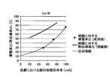
図9A~図9Cは、中心粒径が約9.8μmのタングステン(W)の粉末を添加材として用いた場合の実験(1)~(3)の結果をそれぞれ示すグラフである。このうち、図9Bに示す理論値は、式(1)において、添加材の熱伝導率λaを174W/m・Kとして算出したものである。また、図9Cに示す理論値は、式(2)において、添加材のヤング率Eaを400GPaとし、添加材の熱膨張率αaを4.5×10-6/Kとして算出したものである。
図9Aに示すように、混合粉末における銅の体積含有率に対し、皮膜における銅の体積含有率が多くなっていた。これは、コールドスプレー法で皮膜を形成する場合、タングステンの粉末が皮膜に入り込み難いため、タングステンの体積含有率を、例えば約30%以上といったレベルまで多くすることが困難であることを示している。しかしながら、銅が約70%以上、即ちタングステンが約30%未満の範囲であれば、混合粉末における銅の体積含有率と皮膜における銅の体積含有率との間には概ねリニアな関係が見られるため、粉末の状態における銅とタングステンとの混合比率を調節することにより、皮膜における銅とタングステンとの比率を制御することは可能である。
図9Bに示すように、銅の体積含有率に対する導電率比の実測値は、熱伝導率比の理論値から乖離してしまった。しかしながら、実測値においても、銅の体積含有率に対する導電率比に一定の関係が見られることから、銅とタングステンとの比率を調節することにより、皮膜の導電率比を制御することが可能である。具体的には、銅の体積含有率を約75%以上、即ちタングステンの体積含有率を約25%未満にすることで、導電率比を緩衝層11に好適な50%以上とすることができる。
図9Cに示すように、銅の体積含有率に対する熱膨張率の実測値は、理論値に概ね沿った傾向を示していた。従って、皮膜における銅とタングステンとの比率を調節することにより熱膨張率を制御することが可能であるといえる。例えば、銅の体積含有率を約85%以上、即ちタングステンの体積含有率を約15%未満にすることで、熱膨張率を緩衝層11に好適な13.0×10⁻⁶/K以上16.6×10-6/K未満とすることができる。
従って、図9Aに示す実験結果を考慮すると、緩衝層11に好適な熱伝導率及び熱膨張率を有する皮膜、具体的には銅の体積含有率が85%以上である皮膜をコールドスプレー法により形成するためには、混合粉末における銅の体積含有率を約60%以上、即ちタングステンの体積含有率を約40%未満にすれば良い。
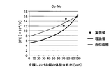
図10A~図10Cは、中心粒径が約5.3μmのモリブデン(Mo)の粉末を添加材として用いた場合の実験(1)~(3)の結果をそれぞれ示すグラフである。このうち、図10Bに示す理論値は、式(1)において、添加材の熱伝導率λaを138W/m・Kとして算出したものである。また、図10Cに示す理論値は、式(2)において、添加材のヤング率Eaを330GPaとし、添加材の熱膨張率αaを4.8×10-6/Kとして算出したものである。
図10Aに示すように、混合粉末における銅の体積含有率に対し、皮膜においては銅の体積含有率が多くなっていた。これは、コールドスプレー法で皮膜を形成する場合、モリブデンの粉末が皮膜に入り込み難いため、モリブデンの体積含有率を、例えば35%以上といったレベルまで多くすることが困難であることを示している。しかしながら、銅が65%以上、即ちモリブデンが35%未満の範囲であれば、混合粉末における銅の体積含有率と皮膜における銅の体積含有率との間には所定の傾向が見られるため、粉末の状態における銅とモリブデンとの混合比率を調節することにより、皮膜における銅とモリブデンとの比率を制御することは可能である。
図10Bに示すように、銅の体積含有率に対する導電率比の実測値は、熱伝導率比の理論値から乖離してしまった。しかしながら、実測値においても、銅の体積含有率に対する導電率比に一定の関係が見られることから、銅とモリブデンとの比率を調節することにより、皮膜の導電率比を制御することは可能である。
ここで、理論的には、銅の体積含有率によらず、導電率比を緩衝層11に好適な50%以上とすることができる。しかしながら、図10Aに示す実験結果を考慮すると、皮膜におけるモリブデンの体積含有率を約35%以上とすることは困難なので、実際には、銅の体積含有率を約65%以上、即ちモリブデンの体積含有率を約35%未満にすることで、上記好適な導電率比を得ることができる。
図10Cに示すように、銅の体積含有率に対する熱膨張率の実測値は、理論値に概ね沿った傾向を示していた。従って、皮膜における銅とモリブデンとの比率を調節することにより、熱膨張率を制御することが可能であるといえる。例えば、銅の体積含有率を約85%以上(モリブデンを約15%未満)とすることで、熱膨張率を緩衝層11に好適な13.0×10⁻⁶/K以上16.6×10-6/K未満とすることができる。
従って、図10Aに示す実験結果を考慮すると、緩衝層11に好適な熱伝導率及び熱膨張率を有する皮膜、具体的には銅の体積含有率が85%以上である皮膜をコールドスプレー法により形成するためには、混合粉末における銅の体積含有率を約65%以上、即ちモリブデンの体積含有率を約35%未満にすれば良い。
図11A及び図11Bは、中心粒径が約30μmのアルミナ(Al2O3)の粉末を添加材として用いた場合の実験(1)及び(3)の結果をそれぞれ示すグラフである。このうち、図11Bに示す理論値は、式(2)において、添加材のヤング率Eaを380GPaとし、添加材の熱膨張率αaを7.2×10⁻⁶/Kとして算出したものである。なお、添加材が金属又は合金でない場合、皮膜の純銅に対する導電率比と純銅に対する熱伝導率比とが対応しないため、導電率比(熱伝導率比)の評価は行っていない。
図11Aに示すように、混合粉末における銅の体積含有率に対し、皮膜における銅の体積含有率が多くなっていた。これは、コールドスプレー法で皮膜を形成する場合、アルミナの粉末が皮膜に入り込み難いことを示している。従って、皮膜においてアルミナの体積含有率を、例えば30%以上といったレベルまで多くする、或いは、混合粉末における銅とアルミナとの混合比率によって皮膜における両者の比率を制御することは困難といえる。
図11Bに示すように、実験データの範囲では、緩衝層11に好適な熱膨張率13.0×10⁻⁶/K以上16.6×10-6/K未満を得ることができた。しかしながら、銅の体積含有率に対する熱膨張率の実測値は、理論値から乖離していたため、銅とアルミナとの比率を調節することにより、皮膜の熱膨張率を制御することは困難といえる。
図12A及び図12Bは、中心粒径が約30μmの炭化ケイ素(SiC)の粉末を添加材として用いた場合の実験(1)及び(3)の結果をそれぞれ示すグラフである。このうち、図12Bに示す理論値は、式(2)において、添加材のヤング率Eaを450GPaとし、添加材の熱膨張率αaを4.4×10⁻⁶/Kとして算出したものである。
図12Aに示すように、混合粉末における銅の体積含有率に対し、皮膜においては銅の体積含有率が多くなっていた。これは、コールドスプレー法で皮膜を形成する場合、炭化ケイ素の粉末が皮膜に入り込み難いことを示している。従って、皮膜において炭化ケイ素の体積含有率を、例えば20%以上といったレベルまで多くする、或いは、混合粉末における銅と炭化ケイ素との混合比率によって皮膜における両者の比率を制御することは困難である。
図12Bに示すように、実験データの範囲では、緩衝層11に好適な熱膨張率13.0×10⁻⁶/K以上16.6×10-6/K未満を得ることができた。しかしながら、銅の体積含有率に対する熱膨張率の実測値は、理論値から乖離していたため、銅の炭化ケイ素との比率を調節することにより、皮膜の熱膨張率を制御することは困難といえる。
図13A及び図13Bは、中心粒径が約25μmの炭素(C)の粉末を添加材として用いた場合の実験(1)及び(3)の結果をそれぞれ示すグラフである。このうち、図13Bに示す理論値は、式(2)において、添加材のヤング率Eaを15GPaとし、添加材の熱膨張率αaを4.4×10⁻⁶/Kとして算出したものである。
図13Aに示すように、混合粉末における銅の体積含有率に対し、皮膜における銅の体積含有率が多くなっていた。これは、コールドスプレー法で皮膜を形成する場合、炭素の粉末が皮膜に入り込み難いことを示している。従って、皮膜において炭素の体積含有率を、例えば10%以上といったレベルまで多くする、或いは、混合粉末における銅と炭素との混合比率によって皮膜における両者の比率を制御することは困難である。
図13Bに示すように、実験データの範囲では、緩衝層11に好適な熱膨張率13.0×10⁻⁶/K以上16.6×10-6/K未満を得ることができた。しかしながら、図13Aに示す実験結果を考慮すると、そもそも、皮膜における銅と炭素との比率を制御することが困難であるので、皮膜の熱膨張率を制御することも困難といえる。
これらの実験結果から、緩衝層11に好適な熱伝導率及び熱膨張率を有する皮膜を形成するためには、添加材として、鉄ニッケル合金、タングステン、又はモリブデンを用い、皮膜における添加材の体積含有率を好ましくは20%未満にすると良い。特に、添加材としてタングステン又はモリブデンを用いる場合には、皮膜における添加材の体積含有率を15%未満にすることが好ましい。
以上説明したように、本実施の形態1によれば、コールドスプレー法を用いることにより、緩衝層11を基板10の金属層17上に直接形成することができる。そのため、絶縁基材13と冷却器12との間における熱応力を緩和することができる。また、従来のパワーモジュールの構成に対し、伝熱シートやグリス等の熱抵抗層を1層省くことができる。従って、基板10において発生した熱を効率良く放出することができ、且つ耐久性に優れたパワーモジュールを実現することが可能となる。
また、本実施の形態1によれば、銅と、鉄ニッケル合金、タングステン、又はモリブデンからなる添加材との混合粉末をコールドスプレー法の材料粉末に適用するので、粉末の混合比率を調節することで、所望の組成比を有する皮膜、言い換えると、所望の熱膨張率や熱伝導率を有する皮膜を容易に形成することができる。また、銅と添加材との粉末の混合比率を調節することにより、皮膜の熱膨張率や熱伝導率を容易に制御することができる。従って、パワーモジュール1における緩衝層11のように、低熱膨張且つ高熱伝導といった要求される特性等に応じた皮膜を容易に実現することができる。また、このような皮膜の組成や特性の制御を、焼結体の場合よりも容易且つ安価に行うことができる。
(実施の形態2)
次に、本発明の実施の形態2について説明する。図14は、本実施の形態2に係るパワーモジュールの構造を示す断面図である。図14に示すパワーモジュール2は、図1に示すパワーモジュール1に対し、緩衝層11が冷却器12の表面(図14においては上面)に直接形成されていると共に、伝熱シート18を介して緩衝層11が基板10の金属層17側に接着されている点が異なる。各部の材料や構成については、実施の形態1と同様である。
次に、本発明の実施の形態2について説明する。図14は、本実施の形態2に係るパワーモジュールの構造を示す断面図である。図14に示すパワーモジュール2は、図1に示すパワーモジュール1に対し、緩衝層11が冷却器12の表面(図14においては上面)に直接形成されていると共に、伝熱シート18を介して緩衝層11が基板10の金属層17側に接着されている点が異なる。各部の材料や構成については、実施の形態1と同様である。
図15は、パワーモジュール2の製造方法を示すフローチャートである。このうち、工程S1及びS2については、実施の形態1と同様である。
工程S2に続く工程S5において、コールドスプレー法により、冷却器12に緩衝層11を形成する。即ち、図3に例示するコールドスプレー装置100において、基材110として冷却器12の基部12aの表面(図14においては上面)をスプレーガン103に向けて配置すると共に、工程S2において調製した混合粉末を粉末供給装置102に投入して、皮膜形成を行う。
続く工程S6において、伝熱シート18を介して、工程S5において形成した緩衝層11に、工程S1において作製した基板10を貼り付ける。それにより、図14に示すパワーモジュール2が完成する。
本実施の形態2によれば、冷却器12側に直接緩衝層11を形成する場合においても、従来のパワーモジュールの構成に対し、伝熱シートやグリス等の熱抵抗層を1層省くことができるので、基板10において発生した熱を効率良く放出することができ、且つ耐久性に優れたパワーモジュールを実現することが可能となる。
1、2、9 パワーモジュール
10、96 基板
11、97 緩衝層
12、98 冷却器
12a 基部
12b 冷却部
13、91 絶縁基材
14、92 回路層
15、93 半田
16、94 半導体チップ
17、95 金属層
18 伝熱シート
100 コールドスプレー装置
101 ガス加熱器
102 粉末供給装置
103 スプレーガン
104 ガスノズル
105、106 バルブ
110 基材
111 皮膜
10、96 基板
11、97 緩衝層
12、98 冷却器
12a 基部
12b 冷却部
13、91 絶縁基材
14、92 回路層
15、93 半田
16、94 半導体チップ
17、95 金属層
18 伝熱シート
100 コールドスプレー装置
101 ガス加熱器
102 粉末供給装置
103 スプレーガン
104 ガスノズル
105、106 バルブ
110 基材
111 皮膜
Claims (5)
- 銅の粉末と、鉄ニッケル合金、タングステン、及びモリブデンのいずれかからなる添加材の粉末とを混合した混合粉末をガスと共に加速し、基材の表面に固相状態のままで吹き付けて堆積させることによって形成され、
前記添加材の体積含有率が0%より大きく20%未満であることを特徴とする複合材。 - 前記鉄ニッケル合金は、Fe-36Ni又はFe-32Ni-5Coであることを特徴とする請求項1に記載の複合材。
- 請求項1又は2に記載の複合材と、
前記基材と、
を備えることを特徴とする積層体。 - 一方の面に半導体素子が実装された基板と、
前記基板の他方の面を前記基材の表面として形成された請求項1~3のいずれか1項に記載の複合材と、
平板状をなす基部と、該基部の一方の面に設けられた冷却部と、を有し、前記基部の他方の面において前記複合材と接着された冷却器と、
を備えることを特徴とするパワーモジュール。 - 平板状をなす基部と、該基部の一方の面に設けられた冷却部と、を有する冷却器と、
前記基部の他方の面を前記基材の表面として形成された請求項1~3のいずれか1項に記載の複合材と、
一方の面に半導体素子が実装され、他方の面において前記複合材に接着された基板と、
を備えることを特徴とするパワーモジュール。
Applications Claiming Priority (2)
| Application Number | Priority Date | Filing Date | Title |
|---|---|---|---|
| JP2014-118183 | 2014-06-06 | ||
| JP2014118183A JP2015231040A (ja) | 2014-06-06 | 2014-06-06 | 積層体、及びパワーモジュール |
Publications (1)
| Publication Number | Publication Date |
|---|---|
| WO2015186643A1 true WO2015186643A1 (ja) | 2015-12-10 |
Family
ID=54766716
Family Applications (1)
| Application Number | Title | Priority Date | Filing Date |
|---|---|---|---|
| PCT/JP2015/065684 Ceased WO2015186643A1 (ja) | 2014-06-06 | 2015-05-29 | 複合材、積層体、及びパワーモジュール |
Country Status (2)
| Country | Link |
|---|---|
| JP (1) | JP2015231040A (ja) |
| WO (1) | WO2015186643A1 (ja) |
Citations (2)
| Publication number | Priority date | Publication date | Assignee | Title |
|---|---|---|---|---|
| JP2008300455A (ja) * | 2007-05-29 | 2008-12-11 | Sumitomo Electric Ind Ltd | パワーモジュール |
| JP4645464B2 (ja) * | 2006-01-27 | 2011-03-09 | トヨタ自動車株式会社 | 電子部材の製造方法 |
-
2014
- 2014-06-06 JP JP2014118183A patent/JP2015231040A/ja active Pending
-
2015
- 2015-05-29 WO PCT/JP2015/065684 patent/WO2015186643A1/ja not_active Ceased
Patent Citations (2)
| Publication number | Priority date | Publication date | Assignee | Title |
|---|---|---|---|---|
| JP4645464B2 (ja) * | 2006-01-27 | 2011-03-09 | トヨタ自動車株式会社 | 電子部材の製造方法 |
| JP2008300455A (ja) * | 2007-05-29 | 2008-12-11 | Sumitomo Electric Ind Ltd | パワーモジュール |
Also Published As
| Publication number | Publication date |
|---|---|
| JP2015231040A (ja) | 2015-12-21 |
Similar Documents
| Publication | Publication Date | Title |
|---|---|---|
| JP6096094B2 (ja) | 積層体、絶縁性冷却板、パワーモジュールおよび積層体の製造方法 | |
| JP5409740B2 (ja) | 放熱構造体、パワーモジュール、放熱構造体の製造方法およびパワーモジュールの製造方法 | |
| Fukumoto et al. | Effects of Extreme Temperature Swings ($-\hbox {55}\^{\circ}\hbox {C} $ to 250$^{\circ}\hbox {C} $) on Silicon Nitride Active Metal Brazing Substrates | |
| US11158560B2 (en) | Thermal structures for dissipating heat and methods for manufacture thereof | |
| KR102084339B1 (ko) | 적층체 및 적층체의 제조 방법 | |
| CN110168140B (zh) | 陶瓷电路基板的制造方法 | |
| WO2013047330A1 (ja) | 接合体 | |
| WO2016021561A1 (ja) | 複合基板及びパワーモジュール | |
| JP5848874B2 (ja) | 温度調節装置およびこの温度調節装置の製造方法 | |
| TW201935624A (zh) | 以陶瓷為基之熱傳導性電源基板之製造方法 | |
| WO2018135490A1 (ja) | セラミックス回路基板の製造方法 | |
| WO2016056567A1 (ja) | 放熱部材用積層体、ヒートシンク付き基板、および放熱部材用積層体の製造方法 | |
| JP5940589B2 (ja) | 積層体、及びパワーモジュール | |
| JP6378247B2 (ja) | 積層体、パワーモジュールおよび積層体の製造方法 | |
| WO2015186643A1 (ja) | 複合材、積層体、及びパワーモジュール | |
| JP4645464B2 (ja) | 電子部材の製造方法 | |
| KR101992749B1 (ko) | 멀티 히트 스프레더 | |
| JP5935517B2 (ja) | ろう材、ろう材による接合方法及び半導体モジュール | |
| US11973002B2 (en) | Composite substrate and method for manufacturing same, and circuit substrate and method for manufacturing same | |
| KR20230104033A (ko) | 구리 접합 질화물 기판용 구리 접합층 니켈 합금 조성물 | |
| JP2010239164A (ja) | 配線基板 |
Legal Events
| Date | Code | Title | Description |
|---|---|---|---|
| 121 | Ep: the epo has been informed by wipo that ep was designated in this application |
Ref document number: 15803102 Country of ref document: EP Kind code of ref document: A1 |
|
| NENP | Non-entry into the national phase |
Ref country code: DE |
|
| 122 | Ep: pct application non-entry in european phase |
Ref document number: 15803102 Country of ref document: EP Kind code of ref document: A1 |