WO2015133013A1 - Electronic apparatus and control method - Google Patents
Electronic apparatus and control method Download PDFInfo
- Publication number
- WO2015133013A1 WO2015133013A1 PCT/JP2014/080408 JP2014080408W WO2015133013A1 WO 2015133013 A1 WO2015133013 A1 WO 2015133013A1 JP 2014080408 W JP2014080408 W JP 2014080408W WO 2015133013 A1 WO2015133013 A1 WO 2015133013A1
- Authority
- WO
- WIPO (PCT)
- Prior art keywords
- solar cell
- resistor
- output voltage
- control circuit
- external data
- Prior art date
Links
- 238000000034 method Methods 0.000 title claims description 30
- 238000004891 communication Methods 0.000 abstract description 36
- 230000005540 biological transmission Effects 0.000 description 49
- 230000003287 optical effect Effects 0.000 description 37
- 238000010586 diagram Methods 0.000 description 6
- 230000006870 function Effects 0.000 description 5
- 238000012545 processing Methods 0.000 description 4
- 238000013500 data storage Methods 0.000 description 1
- 230000007423 decrease Effects 0.000 description 1
- 238000005286 illumination Methods 0.000 description 1
- 239000004973 liquid crystal related substance Substances 0.000 description 1
- 238000012986 modification Methods 0.000 description 1
- 230000004048 modification Effects 0.000 description 1
- 230000002093 peripheral effect Effects 0.000 description 1
- 230000002265 prevention Effects 0.000 description 1
- 238000012546 transfer Methods 0.000 description 1
Images


Classifications
-
- G—PHYSICS
- G04—HOROLOGY
- G04C—ELECTROMECHANICAL CLOCKS OR WATCHES
- G04C10/00—Arrangements of electric power supplies in time pieces
- G04C10/02—Arrangements of electric power supplies in time pieces the power supply being a radioactive or photovoltaic source
-
- G—PHYSICS
- G04—HOROLOGY
- G04G—ELECTRONIC TIME-PIECES
- G04G19/00—Electric power supply circuits specially adapted for use in electronic time-pieces
-
- G—PHYSICS
- G04—HOROLOGY
- G04G—ELECTRONIC TIME-PIECES
- G04G21/00—Input or output devices integrated in time-pieces
- G04G21/04—Input or output devices integrated in time-pieces using radio waves
-
- H—ELECTRICITY
- H01—ELECTRIC ELEMENTS
- H01L—SEMICONDUCTOR DEVICES NOT COVERED BY CLASS H10
- H01L31/00—Semiconductor devices sensitive to infrared radiation, light, electromagnetic radiation of shorter wavelength or corpuscular radiation and specially adapted either for the conversion of the energy of such radiation into electrical energy or for the control of electrical energy by such radiation; Processes or apparatus specially adapted for the manufacture or treatment thereof or of parts thereof; Details thereof
- H01L31/02—Details
- H01L31/02016—Circuit arrangements of general character for the devices
- H01L31/02019—Circuit arrangements of general character for the devices for devices characterised by at least one potential jump barrier or surface barrier
- H01L31/02021—Circuit arrangements of general character for the devices for devices characterised by at least one potential jump barrier or surface barrier for solar cells
-
- H—ELECTRICITY
- H02—GENERATION; CONVERSION OR DISTRIBUTION OF ELECTRIC POWER
- H02J—CIRCUIT ARRANGEMENTS OR SYSTEMS FOR SUPPLYING OR DISTRIBUTING ELECTRIC POWER; SYSTEMS FOR STORING ELECTRIC ENERGY
- H02J7/00—Circuit arrangements for charging or depolarising batteries or for supplying loads from batteries
- H02J7/34—Parallel operation in networks using both storage and other dc sources, e.g. providing buffering
- H02J7/35—Parallel operation in networks using both storage and other dc sources, e.g. providing buffering with light sensitive cells
-
- H—ELECTRICITY
- H02—GENERATION; CONVERSION OR DISTRIBUTION OF ELECTRIC POWER
- H02S—GENERATION OF ELECTRIC POWER BY CONVERSION OF INFRARED RADIATION, VISIBLE LIGHT OR ULTRAVIOLET LIGHT, e.g. USING PHOTOVOLTAIC [PV] MODULES
- H02S40/00—Components or accessories in combination with PV modules, not provided for in groups H02S10/00 - H02S30/00
- H02S40/30—Electrical components
- H02S40/38—Energy storage means, e.g. batteries, structurally associated with PV modules
-
- Y—GENERAL TAGGING OF NEW TECHNOLOGICAL DEVELOPMENTS; GENERAL TAGGING OF CROSS-SECTIONAL TECHNOLOGIES SPANNING OVER SEVERAL SECTIONS OF THE IPC; TECHNICAL SUBJECTS COVERED BY FORMER USPC CROSS-REFERENCE ART COLLECTIONS [XRACs] AND DIGESTS
- Y02—TECHNOLOGIES OR APPLICATIONS FOR MITIGATION OR ADAPTATION AGAINST CLIMATE CHANGE
- Y02E—REDUCTION OF GREENHOUSE GAS [GHG] EMISSIONS, RELATED TO ENERGY GENERATION, TRANSMISSION OR DISTRIBUTION
- Y02E10/00—Energy generation through renewable energy sources
- Y02E10/50—Photovoltaic [PV] energy
-
- Y—GENERAL TAGGING OF NEW TECHNOLOGICAL DEVELOPMENTS; GENERAL TAGGING OF CROSS-SECTIONAL TECHNOLOGIES SPANNING OVER SEVERAL SECTIONS OF THE IPC; TECHNICAL SUBJECTS COVERED BY FORMER USPC CROSS-REFERENCE ART COLLECTIONS [XRACs] AND DIGESTS
- Y02—TECHNOLOGIES OR APPLICATIONS FOR MITIGATION OR ADAPTATION AGAINST CLIMATE CHANGE
- Y02E—REDUCTION OF GREENHOUSE GAS [GHG] EMISSIONS, RELATED TO ENERGY GENERATION, TRANSMISSION OR DISTRIBUTION
- Y02E70/00—Other energy conversion or management systems reducing GHG emissions
- Y02E70/30—Systems combining energy storage with energy generation of non-fossil origin
Definitions
- the present invention relates to an electronic device and a control method.
- the present invention claims priority based on Japanese Patent Application No. 2014-040129 filed in Japan on March 3, 2014, the entire contents of which are incorporated herein by reference.
- An object of the present invention is to provide an electronic device and a control method capable of performing data communication using the.
- Some aspects of the present invention include a solar cell, a receiver that receives data based on an output voltage of the solar cell, a resistor connected between electrodes of the solar cell, and the receiver that receives the data.
- An electronic device comprising: a control unit that controls a resistance value of the resistor based on whether or not the receiving operation is being performed.
- control unit disconnects the resistor when the receiving unit is not in operation to receive the data.
- control unit controls a resistance value of the resistor in accordance with an output voltage of the solar cell.
- control unit reduces the resistance value of the resistor when the output voltage of the solar cell is a predetermined value or more for a predetermined time or more.
- the receiving unit receives data based on the output voltage of the solar cell. Further, the control unit controls the resistance value of the resistor connected between the electrodes of the solar cell based on whether or not the receiving unit is operating to receive data. Thereby, even when the intensity
- FIG. 3 is a circuit diagram illustrating a circuit example of a charge control circuit according to the first embodiment. It is the flowchart which showed the operation
- FIG. 1 is a schematic diagram showing a configuration of a data communication system 1 in the present embodiment.
- the data communication system 1 includes an external data transmission device 10 and an electronic timepiece 20.
- the external data transmission device 10 is an electronic device such as a smartphone, a mobile phone, or a tablet terminal, and includes a light emitting diode 101.
- the electronic timepiece 20 includes a solar cell 201.
- the external data transmission device 10 controls lighting and extinguishing of the light emitting diode 101, and transmits data using light. For example, the external data transmitting apparatus 10 turns on the light emitting diode 101 when transmitting data “1”, and turns off the light emitting diode 101 when transmitting data “0”.
- the electronic timepiece 20 receives data based on the output voltage of the solar cell 201. For example, when the light emitting diode 101 of the external data transmission device 10 is turned on, the solar cell 201 generates an output voltage corresponding to the light of the light emitting diode 101.
- the electronic timepiece 20 receives the data “1” when the output voltage of the solar cell 201 is equal to or higher than the predetermined threshold, and receives the data “0” when the output voltage of the solar cell 201 is lower than the predetermined threshold.
- the data transmitted by the external data transmitting apparatus 10 may be any data such as time information.
- FIG. 2 is a schematic diagram showing the configuration of the electronic timepiece 20 in the present embodiment.
- the electronic timepiece 20 includes a solar battery 201, a control circuit 202, a charge control circuit 203, a secondary battery 204, a resistor 205, a transistor 206, an external input unit 207, and a display unit 208. It has.
- the solar cell 201 functions as a generator that receives an external light source (sun, illumination, etc.) and converts it into electrical energy during the charging period, and performs optical communication with the external data transmission device 10 during the communication period. Function as an optical receiver for
- the potential of the cathode terminal of the solar cell 201 is set as a reference potential.
- the resistor 205 is provided between the pair of electrodes of the anode terminal and the cathode terminal of the solar cell 201, and is configured to be connected in parallel with the solar cell 201.
- the transistor 206 has a source terminal grounded and a drain connected to one end of the resistor 205. In short, the transistor 206 is connected between the resistor 205 and the ground (GND). With this configuration, the connection state of the resistor 205 provided between the electrodes of the solar cell 201 can be controlled by switching between the ON state and the OFF state of the transistor 206.
- the control circuit 202 controls each unit included in the electronic timepiece 20.
- the control circuit 202 operates as a communication unit (reception unit). Specifically, in the communication mode (during operation of receiving data), the control circuit 202 detects the output voltage of the solar cell 201 input to the input terminal, and converts the detected voltage into an electric signal. Thus, data transmitted from the external device (in this case, the external data transmission device 10) by optical communication is received. Further, the control circuit 202 controls ON / OFF of the transistor 206 via the control terminal, and controls connection of the resistor 205 connected between the electrodes of the solar cell 201. A method for controlling the connection of the resistor 205 will be described later.
- the external input unit 207 is, for example, a switch or the like, and accepts an operation input from the outside.
- the display unit 208 is a liquid crystal display, for example, and displays information such as time.
- the charging control circuit 203 controls charging control of the secondary battery 204 by the solar battery 201, prevention of overcharging of the secondary battery 204, and the like.
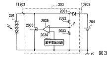
- FIG. 3 is a circuit diagram illustrating a configuration example of the charging control circuit 203.
- the charge control circuit 203 includes a diode element 2031, resistors 2032 and 2033, a reference voltage circuit 2034, a comparator unit 2035, and a transistor 2036.
- the anode terminal of the solar battery 201 is connected to the input terminal TI 203 of the charge control circuit 203, and the anode terminal of the secondary battery 204 is connected to the output terminal TO 203 of the charge control circuit 203.
- the reference potential of the charging control circuit 203 is configured to be a common potential VG between the cathode terminal of the solar battery 201 and the cathode terminal of the secondary battery.
- the anode terminal of the diode element 2031 is connected to the input terminal TI 203 of the charge control circuit 203.
- the cathode terminal of the diode element 2031 is connected to the output terminal TO203 of the charge control circuit 203.
- the charging control circuit 203 causes a current flowing from the anode terminal of the solar battery 201 to the anode terminal of the secondary battery 204, and in contrast, from the anode terminal of the secondary battery 204 to the anode terminal of the solar battery 201. Prevent current from flowing.
- the resistor 2032 and the resistor 2033 are connected in series via the connection point P.
- the other end different from the connection point P of the resistor 2032 is connected to the input terminal TI203 of the charge control circuit 203, and the other end different from the connection point P of the resistor 2033 is configured to be the above-described common potential VG.
- the potential at the connection point P is a potential obtained by dividing the output voltage (Vsc) of the solar cell 201 by the resistor 2032 and the resistor 2033, and can be compared with a reference voltage output by a reference voltage circuit 2034 described later.
- Each resistance value of the resistor 2032 and the resistor 2033 is set so as to be a voltage.
- One end (non-inverting input) of the input terminal of the comparator unit 2035 is connected to the connection point P, and the other end (inverting input) of the input terminal is connected to the output terminal of the reference voltage circuit 2034.
- the output terminal of the comparator unit 2035 is connected to the gate terminal of the transistor 2036.
- the drain terminal of the transistor 2036 is connected to the input terminal TI203 of the charge control circuit 203, and the source terminal is configured to have the above-described common potential VG.
- the drain terminal of the transistor 2036 is connected to the anode terminal of the solar cell 201, and the source terminal is connected to the cathode terminal of the solar cell 201.
- the reference voltage circuit 2034 outputs a reference voltage that is not affected by fluctuations in the output voltage of the solar battery 201, and supplies the reference voltage Vref to the comparator unit 2035.
- the comparator unit 2035 receives the reference voltage Vref and compares the voltage VC obtained by dividing the output voltage of the solar cell 210 with the resistor 2032 and the resistor 2033 with the reference voltage Vref.
- the comparator unit 2035 outputs a voltage corresponding to the comparison result from the output terminal.
- the comparator unit 2035 sets a voltage for turning on the transistor 2036, and when the voltage VC does not exceed the reference voltage Vref (VC ⁇ Vref). In this case, a voltage for turning off the transistor 2036 is applied from the output terminal to the gate of the transistor 2036.
- the output voltage of the solar cell 201 can be made lower than the upper limit voltage of the secondary battery 204, and the overcharge of the secondary battery 204 can be prevented.
- the above-described state in which the transistor 2036 allows the current to flow may be, for example, a state in which the current value is limited by a predetermined internal impedance of the transistor 2036 and does not need to be in a complete ON state. In that case, the internal impedance of the transistor 2036 is adjusted so that the output voltage of the solar battery 201 is lower than the upper limit voltage of the secondary battery 204.
- the output voltage of the solar cell 201 changes according to the intensity of the received light
- the output voltage of the solar cell 201 is the value of the charge control circuit 203 even if the intensity of the light is changed when the intensity of the light is a certain level or more. It becomes a certain upper limit by work. Therefore, when the intensity of ambient light is high and the solar cell 201 is always irradiated with light of a certain level or higher, the output of the solar cell 201 is output even when the external data transmission device 10 turns on and off the light emitting diode 101. The voltage remains unchanged at a certain upper limit.
- the control circuit 202 connects the resistor 205 between the electrodes of the solar cell 201 to Only when light brighter than light is received, the output voltage of the solar cell 201 is set to be equal to or higher than a predetermined threshold. Therefore, for example, the resistance value of the resistor 205 is a value at which the output voltage of the solar cell 201 is equal to or higher than a predetermined threshold only when the resistor 205 is connected between the electrodes of the solar cell 201 and light brighter than ambient light is received.
- the control circuit 202 sets the resistance 205 between the electrodes of the solar cell 201. Disconnect the connection.
- FIG. 4 is a flowchart showing an operation procedure of the electronic timepiece 20 in the present embodiment.
- Step S101 The user operates the external input unit 207 to input an instruction to change to the communication mode when the electronic timepiece 20 receives data transmitted from the external data transmitting apparatus 10.
- the control circuit 202 determines whether or not the external input unit 207 has received an input of a change instruction to the communication mode. If the control circuit 202 determines that an input of an instruction to change to the communication mode has been received, the process proceeds to step S102, and otherwise, the process of step S101 is repeated again.
- Step S102 The control circuit 202 switches the operation mode of the electronic timepiece 20 to the communication mode. Thereafter, the process proceeds to step S103.
- Step S103 The control circuit 202 enables the control terminal and turns on the transistor 206. That is, the control circuit 202 connects the resistor 205 between the electrodes of the solar cell 201. Thereafter, the process proceeds to step S104.
- Step S104 The control circuit 202 detects the output voltage of the solar cell 201 input to the input terminal, and converts the detected voltage into an electrical signal, thereby transmitting data transmitted from the external data transmission device 10 by optical communication. Receive. If the reception of data is completed, the process proceeds to step S105, and if not completed, the process of step S104 is continued.
- Step S105 The control circuit 202 processes the data received in the process of step S104. Thereafter, the process proceeds to step S106.
- Step S106 The control circuit 202 switches the operation mode of the electronic timepiece 20 to the normal mode. Thereafter, the process proceeds to step S107.
- Step S107 The control circuit 202 disables the control terminal and turns off the transistor 206. That is, the control circuit 202 disconnects the resistor 205 between the electrodes of the solar cell 201. Thereafter, the process ends.
- the electronic timepiece 20 is in a communication mode in which data transmitted from the external data transmission device 10 is transmitted by optical communication and in a normal mode in which data reception is not performed. Operate.
- the control circuit 202 connects the resistor 205 between the electrodes of the solar cell 201. Further, the control circuit 202 disconnects the resistor 205 between the electrodes of the solar cell 201 when operating in the normal mode.
- the electronic timepiece 20 when operating in the communication mode, the electronic timepiece 20 detects the output voltage of the solar cell 201 input to the input terminal regardless of the influence of ambient light, and converts the detected voltage into an electric signal. Thus, the data transmitted from the external data transmission device 10 by optical communication is received. Further, when the electronic timepiece 20 operates in the normal mode, the secondary battery 204 can be charged by ambient light. That is, the electronic timepiece 20 can charge the secondary battery 204 even when the intensity of light applied to the solar cell 201 is weak, and performs data communication using the solar cell 201 while suppressing the influence of ambient light. be able to.
- FIG. 5 is a schematic diagram showing the configuration of the electronic timepiece 30 in the present embodiment.
- the electronic timepiece 30 includes a solar battery 201, a control circuit 202, a charge control circuit 203, a secondary battery 204, resistors 301 and 302, transistors 303 and 304, an external input unit 207, And a display unit 208.
- the solar cell 201, the control circuit 202, the charge control circuit 203, the secondary battery 204, the external input unit 207, and the display unit 208 are the same as the respective units of the first embodiment.
- the resistors 301 and 302 are connected in parallel between the electrodes of the solar cell 201.
- the transistor 303 is connected between the resistor 301 and the ground (GND).
- the transistor 304 is connected between the resistor 302 and the ground (GND).
- the control circuit 202 When the intensity of the ambient light is strong, even if only the resistor 301 is connected between the electrodes of the solar cell 201, the output voltage of the solar cell 201 is always equal to or higher than the threshold value Vth. Therefore, even if only the resistor 301 is connected between the electrodes of the solar cell 201, if the intensity of ambient light is strong, even if the external data transmitting device 10 turns on and off the light emitting diode 101, the solar cell 201 The output voltage remains unchanged from the threshold value Vth.
- FIG. 6 is a schematic diagram showing the output voltage of the solar cell 201 when receiving the optical signal transmitted by the external data transmitting device 10 when only the resistor 301 is connected between the electrodes of the solar cell 201 in this embodiment.
- the control circuit 202 determines that the data “1” has been received when the output voltage of the solar cell 201 is equal to or higher than the threshold value Vth, and the data “0” when the output voltage of the solar cell 201 is lower than the threshold value Vth. Is determined to have been received.
- the intensity of ambient light is in the order of a ⁇ b ⁇ c ⁇ d. That is, strength a is the weakest and strength d is the strongest.
- Vbatt is a voltage output when the secondary battery 204 is fully charged.
- Graph (A) shows the intensity of the optical signal transmitted by the external data transmitter 10.
- the optical signal is a signal in which ON and OFF are alternately repeated. That is, the external data transmitter 10 turns on the light emitting diode 101 when turned on, and turns off the light emitting diode 101 when turned off.
- Graph (B) is a graph showing the output voltage of solar cell 201 when an optical signal transmitted from external data transmission device 10 is received when the intensity of ambient light is a.
- the output voltage of the solar cell 201 is equal to or higher than the threshold value Vth.
- the electronic timepiece 30 can receive the optical signal transmitted from the external data transmission device 10.
- Graph (C) is a graph showing the output voltage of solar cell 201 when an optical signal transmitted from external data transmission device 10 is received when the intensity of ambient light is b.
- the output voltage of the solar cell 201 is equal to or higher than the threshold value Vth.
- the electronic timepiece 30 can receive the optical signal transmitted from the external data transmission device 10.
- Graph (D) is a graph showing the output voltage of solar cell 201 when an optical signal transmitted from external data transmission device 10 is received when the intensity of ambient light is c.
- the output voltage of the solar cell 201 is equal to or higher than the threshold value Vth.
- the electronic timepiece 30 cannot receive the optical signal transmitted from the external data transmission device 10.
- Graph (E) is a graph showing the output voltage of solar cell 201 when an optical signal transmitted by external data transmission device 10 is received when the intensity of ambient light is d.
- the output voltage of the solar cell 201 is equal to or higher than the threshold value Vth.
- the electronic timepiece 30 cannot receive the optical signal transmitted from the external data transmission device 10.
- the electronic timepiece 30 cannot receive the optical signal transmitted from the external data transmission device 10. There is a case.
- a resistor 301 and a resistor 302 are connected in parallel between the electrodes of the solar cell 201. That is, the resistance value of the resistor connected between the electrodes of the solar cell 201 is lowered.
- FIG. 7 shows the output of the solar cell 201 when receiving an optical signal transmitted by the external data transmission device 10 when the resistor 301 and the resistor 302 are connected in parallel between the electrodes of the solar cell 201 in this embodiment. It is the schematic which showed the voltage.
- the control circuit 202 determines that the data “1” has been received when the output voltage of the solar cell 201 is equal to or higher than the threshold value Vth, and the data “0” when the output voltage of the solar cell 201 is lower than the threshold value Vth. Is determined to have been received.
- the intensity of ambient light is in the order of a ⁇ b ⁇ c ⁇ d. That is, strength a is the weakest and strength d is the strongest.
- Vbatt is a voltage output when the secondary battery 204 is fully charged.
- Graph (A) shows the intensity of the optical signal transmitted by the external data transmitter 10.
- the optical signal is a signal in which ON and OFF are alternately repeated. That is, the external data transmitter 10 turns on the light emitting diode 101 when turned on, and turns off the light emitting diode 101 when turned off.
- Graph (B) is a graph showing the output voltage of solar cell 201 when an optical signal transmitted from external data transmission device 10 is received when the intensity of ambient light is a.
- the output voltage of the solar cell 201 is less than the threshold value Vth.
- the electronic timepiece 30 cannot receive the optical signal transmitted from the external data transmission device 10.
- Graph (C) is a graph showing the output voltage of solar cell 201 when an optical signal transmitted from external data transmission device 10 is received when the intensity of ambient light is b.
- the output voltage of the solar cell 201 is equal to or higher than the threshold value Vth.
- the electronic timepiece 30 can receive the optical signal transmitted from the external data transmission device 10.
- Graph (D) is a graph showing the output voltage of solar cell 201 when an optical signal transmitted from external data transmission device 10 is received when the intensity of ambient light is c.
- the output voltage of the solar cell 201 is equal to or higher than the threshold value Vth.
- the electronic timepiece 30 can receive the optical signal transmitted from the external data transmission device 10.
- Graph (E) is a graph showing the output voltage of solar cell 201 when an optical signal transmitted by external data transmission device 10 is received when the intensity of ambient light is d.
- the output voltage of the solar cell 201 is equal to or higher than the threshold value Vth.
- the electronic timepiece 30 can receive the optical signal transmitted from the external data transmission device 10.
- the electronic timepiece 30 transmits the optical signal transmitted from the external data transmission device 10 by connecting the resistor 301 and the resistor 302 in parallel between the electrodes of the solar cell 201. Can be received.
- the electronic timepiece 30 may not be able to receive an optical signal transmitted from the external data transmission device 10.
- the resistor 301 and the resistor 302 are interposed between the electrodes of the solar cell 201. Are connected in parallel. That is, when operating in the communication mode, if the output voltage of the solar cell 201 continues for a predetermined time or more than the threshold value Vth, the resistance value of the resistor connected between the electrodes of the solar cell 201 is lowered. Thereby, the electronic timepiece 30 can receive an optical signal transmitted from the external data transmitting apparatus 10 regardless of the intensity of ambient light.
- FIG. 8 is a flowchart showing an operation procedure of the electronic timepiece 30 in the present embodiment.
- the processing from step S201 to step S202 is the same as the processing from step S101 to step S102 in the first embodiment.
- Step S203 The control circuit 202 enables the control terminal 1 and turns on the transistor 303. That is, the control circuit 202 connects the resistor 301 between the electrodes of the solar cell 201. Thereafter, the process proceeds to step S204.
- Step S204 The control circuit 202 determines whether or not the output voltage of the secondary battery 204 has continued for not less than the threshold value Vth and not less than a predetermined time. If the control circuit 202 determines that the output voltage of the secondary battery 204 has exceeded the threshold value Vth and has continued for a predetermined time or longer, the process proceeds to step S205, and otherwise, the process proceeds to step S206.
- Step S205 The control circuit 202 enables the control terminal 2 and turns on the transistor 304. That is, the control circuit 202 connects the resistor 302 between the electrodes of the solar cell 201. Thereafter, the process proceeds to step S206.
- step S206 to step S208 is the same as the processing from step S104 to step S106 in the first embodiment.
- Step S209 The control circuit 202 disables the control terminals 1 and 2 and turns off the transistors 303 and 304. That is, the control circuit 202 disconnects the resistors 301 and 302 between the electrodes of the solar cell 201. Thereafter, the process ends.
- the electronic timepiece 30 is in a communication mode in which data transmitted from the external data transmission device 10 is transmitted by optical communication and in a normal mode in which data reception is not performed. Operate.
- the control circuit 202 disconnects the resistors 301 and 302 between the electrodes of the solar cell 201.
- the control circuit 202 connects the resistor 301 between the electrodes of the solar cell 201 when operating in the communication mode. Further, even when the resistor 301 is connected between the electrodes of the solar cell 201, when the output voltage of the solar cell 210 continues for a predetermined time or more than the threshold Vth, the resistor 301 and A resistor 302 is connected in parallel.
- the electronic timepiece 30 when operating in the communication mode, the electronic timepiece 30 detects the output voltage of the solar cell 201 input to the input terminal regardless of the influence of ambient light, and converts the detected voltage into an electric signal. Thus, it is possible to receive data transmitted from the external data transmission device 10 by optical communication.
- the secondary battery 204 can be charged with ambient light. That is, the electronic timepiece 30 can charge the secondary battery 204 even when the intensity of light applied to the solar cell 201 is weak, and performs data communication using the solar cell 201 while suppressing the influence of ambient light. be able to.
- the present invention is not limited thereto.
- three or more resistors may be connected between the electrodes of the solar cell 201.
- the connection of the resistors is not limited to parallel, and may be connected in series.
- a variable resistor may be used as the resistor.
- each unit included in the electronic device 20 or the electronic timepiece 30 in the embodiment described above is recorded on a computer-readable recording medium, and this recording medium It may be realized by reading the program recorded in the above into a computer system and executing it.
- the “computer system” includes an OS and hardware such as peripheral devices.
- the “computer-readable recording medium” means a portable medium such as a flexible disk, a magneto-optical disk, a ROM, and a CD-ROM, and a storage unit such as a hard disk built in the computer system. Furthermore, the “computer-readable recording medium” dynamically holds a program for a short time like a communication line when transmitting a program via a network such as the Internet or a communication line such as a telephone line. In this case, a volatile memory inside a computer system serving as a server or a client in that case may be included and a program that holds a program for a certain period of time.
- the program may be a program for realizing a part of the functions described above, and may be a program capable of realizing the functions described above in combination with a program already recorded in a computer system.
- the electronic timepieces 20 and 30 are described as examples of the electronic device.
- the present invention is not limited to this, and any electronic device may be used as long as the electronic device includes a solar battery.
- the connection of the resistors 205, 301, and 302 connected between the electrodes of the solar cell 201 is controlled by ON / OFF of the transistors 206, 303, and 304. You may control by a method.
- the light source used by the external data transmission device 10 to transmit an optical signal is not limited to the light emitting diode 101, and any light source that can be turned on and off may be used.
- SYMBOLS 1 Data communication system, 10 ... External data transmitter, 20, 30 ... Electronic timepiece, 101 ... Light emitting diode, 201 ... Solar cell, 202 ... Control circuit, 203 ... Charge control circuit, 204 ... secondary battery, 205, 301, 302, 2032, 2033 ... resistor, 206, 303, 304, 2036 ... transistor, 207 ... external input unit, 208 ... Display unit 2031 ... Diode element 2034 ... Reference voltage circuit 2035 ... Comparator unit
Landscapes
- Engineering & Computer Science (AREA)
- Power Engineering (AREA)
- Physics & Mathematics (AREA)
- General Physics & Mathematics (AREA)
- Electromagnetism (AREA)
- Sustainable Development (AREA)
- Sustainable Energy (AREA)
- Condensed Matter Physics & Semiconductors (AREA)
- Life Sciences & Earth Sciences (AREA)
- Computer Hardware Design (AREA)
- Microelectronics & Electronic Packaging (AREA)
- Electromechanical Clocks (AREA)
- Optical Communication System (AREA)
- Electric Clocks (AREA)
- Photovoltaic Devices (AREA)
- Charge And Discharge Circuits For Batteries Or The Like (AREA)
Abstract
Description
本発明は、2014年3月3日に日本に出願された特願2014-040129に基づき優先権を主張し、同出願の全記載内容を本書において引用する。 The present invention relates to an electronic device and a control method.
The present invention claims priority based on Japanese Patent Application No. 2014-040129 filed in Japan on March 3, 2014, the entire contents of which are incorporated herein by reference.
まず、本発明の第1の実施形態について説明する。図1は、本実施形態におけるデータ通信システム1の構成を示した概略図である。図示する例では、データ通信システム1は、外部データ送信装置10と、電子時計20とを含んでいる。外部データ送信装置10は、例えば、スマートフォンや、携帯電話機や、タブレット端末等の電子機器であり、発光ダイオード101を備えている。電子時計20は、太陽電池201を備えている。 (First embodiment)
First, a first embodiment of the present invention will be described. FIG. 1 is a schematic diagram showing a configuration of a
(ステップS101)ユーザは、電子時計20に外部データ送信装置10から送信されるデータを受信させる場合には、外部入力部207を操作し、通信モードへの変更指示を入力する。制御回路202は、外部入力部207が通信モードへの変更指示の入力を受け付けたか否かを判定する。通信モードへの変更指示の入力を受け付けたと制御回路202が判定した場合にはステップS102の処理に進み、それ以外の場合には再度ステップS101の処理を繰り返す。 Next, the operation procedure of the
(Step S101) The user operates the
(ステップS103)制御回路202は、制御端子をイネーブルにし、トランジスタ206をONにする。すなわち、制御回路202は、太陽電池201の電極間に抵抗205を接続させる。その後、ステップS104の処理に進む。 (Step S102) The
(Step S103) The
(ステップS106)制御回路202は、電子時計20の動作モードを通常モードに切り替える。その後、ステップS107の処理に進む。 (Step S105) The
(Step S106) The
次に、本発明の第2の実施形態について説明する。本実施形態と第1の実施形態とで異なる点は、太陽電池201の電極間に接続されている抵抗の抵抗値を変更することができる点である。 (Second Embodiment)
Next, a second embodiment of the present invention will be described. The difference between the present embodiment and the first embodiment is that the resistance value of the resistor connected between the electrodes of the
ステップS201~ステップS202の処理は、第1の実施形態におけるステップS101~ステップS102の処理と同様である。 Next, the operation procedure of the
The processing from step S201 to step S202 is the same as the processing from step S101 to step S102 in the first embodiment.
(ステップS209)制御回路202は、制御端子1,2をディスエーブルにし、トランジスタ303,304をOFFにする。すなわち、制御回路202は、太陽電池201の電極間の抵抗301,302の接続を切断させる。その後、処理を終了する。 The processing from step S206 to step S208 is the same as the processing from step S104 to step S106 in the first embodiment.
(Step S209) The
Claims (5)
- 太陽電池と、
前記太陽電池の出力電圧に基づいてデータを受信する受信部と、
前記太陽電池の電極間に接続された抵抗と、
前記受信部が前記データを受信する動作中であるか否かに基づいて、前記抵抗の抵抗値を制御する制御部と、
を備えることを特徴とする電子機器。 Solar cells,
A receiver for receiving data based on the output voltage of the solar cell;
A resistor connected between the electrodes of the solar cell;
A control unit that controls a resistance value of the resistor based on whether the receiving unit is operating to receive the data;
An electronic device comprising: - 前記制御部は、前記受信部が前記データを受信する動作中ではない場合、前記抵抗の接続を切断する
ことを特徴とする請求項1に記載の電子機器。 The electronic device according to claim 1, wherein the control unit disconnects the resistor when the receiving unit is not in an operation of receiving the data. - 前記制御部は、前記太陽電池の出力電圧に応じて前記抵抗の抵抗値を制御する
ことを特徴とする請求項1または請求項2に記載の電子機器。 The electronic device according to claim 1, wherein the control unit controls a resistance value of the resistor in accordance with an output voltage of the solar cell. - 前記制御部は、所定時間以上、前記太陽電池の出力電圧が一定値以上の場合、前記抵抗の抵抗値を小さくする
ことを特徴とする請求項3に記載の電子機器。 The electronic device according to claim 3, wherein the control unit reduces the resistance value of the resistor when the output voltage of the solar cell is a predetermined value or more for a predetermined time or more. - 太陽電池の出力電圧に基づいてデータを受信する受信ステップと、
前記受信ステップで前記データを受信する動作中であるか否かに基づいて、前記太陽電池の電極間に接続された抵抗の抵抗値を制御する制御ステップと、
を含むことを特徴とする制御方法。 A receiving step for receiving data based on the output voltage of the solar cell;
A control step of controlling a resistance value of a resistor connected between the electrodes of the solar cell based on whether or not the data is received in the receiving step;
The control method characterized by including.
Priority Applications (2)
| Application Number | Priority Date | Filing Date | Title |
|---|---|---|---|
| US15/122,619 US10228660B2 (en) | 2014-03-03 | 2014-11-18 | Electronic apparatus and control method |
| JP2016506080A JP6395806B2 (en) | 2014-03-03 | 2014-11-18 | Electronic device and control method |
Applications Claiming Priority (2)
| Application Number | Priority Date | Filing Date | Title |
|---|---|---|---|
| JP2014-040129 | 2014-03-03 | ||
| JP2014040129 | 2014-03-03 |
Publications (1)
| Publication Number | Publication Date |
|---|---|
| WO2015133013A1 true WO2015133013A1 (en) | 2015-09-11 |
Family
ID=54054836
Family Applications (1)
| Application Number | Title | Priority Date | Filing Date |
|---|---|---|---|
| PCT/JP2014/080408 WO2015133013A1 (en) | 2014-03-03 | 2014-11-18 | Electronic apparatus and control method |
Country Status (3)
| Country | Link |
|---|---|
| US (1) | US10228660B2 (en) |
| JP (1) | JP6395806B2 (en) |
| WO (1) | WO2015133013A1 (en) |
Families Citing this family (2)
| Publication number | Priority date | Publication date | Assignee | Title |
|---|---|---|---|---|
| JP6547379B2 (en) * | 2015-04-10 | 2019-07-24 | セイコーエプソン株式会社 | Communication system, electronic watch and communication device |
| DE102017111946A1 (en) * | 2017-05-31 | 2018-12-06 | Epcos Ag | Electrical circuit and use of electrical circuit |
Citations (5)
| Publication number | Priority date | Publication date | Assignee | Title |
|---|---|---|---|---|
| JPS5533324A (en) * | 1978-08-30 | 1980-03-08 | Hitachi Ltd | Remote control receiver |
| JPH052879Y2 (en) * | 1987-06-29 | 1993-01-25 | ||
| JPH10239464A (en) * | 1996-12-25 | 1998-09-11 | Casio Comput Co Ltd | Electronic equipment with solar battery |
| JP2001099964A (en) * | 1999-09-30 | 2001-04-13 | Seiko Epson Corp | Electronic watch and control method of electronic watch |
| WO2012132874A1 (en) * | 2011-03-31 | 2012-10-04 | シチズンホールディングス株式会社 | Radio-controlled wristwatch |
Family Cites Families (3)
| Publication number | Priority date | Publication date | Assignee | Title |
|---|---|---|---|---|
| US4240021A (en) * | 1977-05-20 | 1980-12-16 | Citizen Watch Co., Ltd. | Solar cell battery charging control system |
| US4571532A (en) * | 1983-11-03 | 1986-02-18 | Gte Automatic Electric Incorporated | Photovoltaic power regulation system |
| US5886954A (en) | 1997-08-20 | 1999-03-23 | Casio Computer Co., Ltd. | Electronic devices with a solar cell |
-
2014
- 2014-11-18 WO PCT/JP2014/080408 patent/WO2015133013A1/en active Application Filing
- 2014-11-18 US US15/122,619 patent/US10228660B2/en active Active
- 2014-11-18 JP JP2016506080A patent/JP6395806B2/en active Active
Patent Citations (5)
| Publication number | Priority date | Publication date | Assignee | Title |
|---|---|---|---|---|
| JPS5533324A (en) * | 1978-08-30 | 1980-03-08 | Hitachi Ltd | Remote control receiver |
| JPH052879Y2 (en) * | 1987-06-29 | 1993-01-25 | ||
| JPH10239464A (en) * | 1996-12-25 | 1998-09-11 | Casio Comput Co Ltd | Electronic equipment with solar battery |
| JP2001099964A (en) * | 1999-09-30 | 2001-04-13 | Seiko Epson Corp | Electronic watch and control method of electronic watch |
| WO2012132874A1 (en) * | 2011-03-31 | 2012-10-04 | シチズンホールディングス株式会社 | Radio-controlled wristwatch |
Also Published As
| Publication number | Publication date |
|---|---|
| US20170075310A1 (en) | 2017-03-16 |
| US10228660B2 (en) | 2019-03-12 |
| JP6395806B2 (en) | 2018-09-26 |
| JPWO2015133013A1 (en) | 2017-04-06 |
Similar Documents
| Publication | Publication Date | Title |
|---|---|---|
| US11139652B2 (en) | System and method for a load-based selectable battery cell | |
| KR101902951B1 (en) | Charging circuit and terminal | |
| US9906059B2 (en) | Charge and discharge management system and movable power source using the same | |
| US10727677B2 (en) | Fast charging circuit | |
| US9859726B2 (en) | Detection circuit and method for starting charging | |
| US11128154B2 (en) | Charging method and related device | |
| KR20100082036A (en) | Bidirectional power management techniques | |
| JP2008178196A (en) | Power receiving controller, power receiver, and electronic apparatus | |
| US20170294794A1 (en) | Electronic system and charging method | |
| US9864130B2 (en) | Power supply system | |
| US20130181683A1 (en) | Battery Charging Circuit and Reference Signal Generator | |
| CN105515173A (en) | Wearable device and method thereof for managing application program according to electric quantity | |
| JP6395806B2 (en) | Electronic device and control method | |
| US20150325960A1 (en) | Universal serial bus interface and mobile device | |
| US11336106B2 (en) | Charging system with low power consumption | |
| CN102255362A (en) | Power supply device and method for terminal | |
| US9991700B2 (en) | Power bank, power bank system and method thereof | |
| JP2019103305A (en) | Power supply device and communication device | |
| US20130003428A1 (en) | Power supply system and electrical device with same | |
| US20140217994A1 (en) | Electronic device with fast charging circuit | |
| US10367371B2 (en) | Intelligent charging system and intelligent charging method | |
| CN110649673A (en) | Mobile terminal | |
| CN116742106B (en) | Battery module, charging control method and electronic equipment | |
| CN118157251A (en) | Charging circuit control method and device, terminal equipment and storage medium | |
| US20130106345A1 (en) | Charger for reducing static power consumption |
Legal Events
| Date | Code | Title | Description |
|---|---|---|---|
| 121 | Ep: the epo has been informed by wipo that ep was designated in this application |
Ref document number: 14884334 Country of ref document: EP Kind code of ref document: A1 |
|
| ENP | Entry into the national phase |
Ref document number: 2016506080 Country of ref document: JP Kind code of ref document: A |
|
| WWE | Wipo information: entry into national phase |
Ref document number: 15122619 Country of ref document: US |
|
| NENP | Non-entry into the national phase |
Ref country code: DE |
|
| 122 | Ep: pct application non-entry in european phase |
Ref document number: 14884334 Country of ref document: EP Kind code of ref document: A1 |