WO2015098608A1 - タッチパネル製造方法 - Google Patents
タッチパネル製造方法 Download PDFInfo
- Publication number
- WO2015098608A1 WO2015098608A1 PCT/JP2014/083206 JP2014083206W WO2015098608A1 WO 2015098608 A1 WO2015098608 A1 WO 2015098608A1 JP 2014083206 W JP2014083206 W JP 2014083206W WO 2015098608 A1 WO2015098608 A1 WO 2015098608A1
- Authority
- WO
- WIPO (PCT)
- Prior art keywords
- conductive
- bridge wiring
- touch panel
- insulating film
- electrode
- Prior art date
- Legal status (The legal status is an assumption and is not a legal conclusion. Google has not performed a legal analysis and makes no representation as to the accuracy of the status listed.)
- Ceased
Links
Images






Classifications
-
- G—PHYSICS
- G06—COMPUTING OR CALCULATING; COUNTING
- G06F—ELECTRIC DIGITAL DATA PROCESSING
- G06F3/00—Input arrangements for transferring data to be processed into a form capable of being handled by the computer; Output arrangements for transferring data from processing unit to output unit, e.g. interface arrangements
- G06F3/01—Input arrangements or combined input and output arrangements for interaction between user and computer
- G06F3/03—Arrangements for converting the position or the displacement of a member into a coded form
- G06F3/041—Digitisers, e.g. for touch screens or touch pads, characterised by the transducing means
- G06F3/044—Digitisers, e.g. for touch screens or touch pads, characterised by the transducing means by capacitive means
- G06F3/0446—Digitisers, e.g. for touch screens or touch pads, characterised by the transducing means by capacitive means using a grid-like structure of electrodes in at least two directions, e.g. using row and column electrodes
-
- G—PHYSICS
- G06—COMPUTING OR CALCULATING; COUNTING
- G06F—ELECTRIC DIGITAL DATA PROCESSING
- G06F3/00—Input arrangements for transferring data to be processed into a form capable of being handled by the computer; Output arrangements for transferring data from processing unit to output unit, e.g. interface arrangements
- G06F3/01—Input arrangements or combined input and output arrangements for interaction between user and computer
- G06F3/03—Arrangements for converting the position or the displacement of a member into a coded form
- G06F3/041—Digitisers, e.g. for touch screens or touch pads, characterised by the transducing means
- G06F3/044—Digitisers, e.g. for touch screens or touch pads, characterised by the transducing means by capacitive means
- G06F3/0443—Digitisers, e.g. for touch screens or touch pads, characterised by the transducing means by capacitive means using a single layer of sensing electrodes
-
- G—PHYSICS
- G06—COMPUTING OR CALCULATING; COUNTING
- G06F—ELECTRIC DIGITAL DATA PROCESSING
- G06F2203/00—Indexing scheme relating to G06F3/00 - G06F3/048
- G06F2203/041—Indexing scheme relating to G06F3/041 - G06F3/045
- G06F2203/04103—Manufacturing, i.e. details related to manufacturing processes specially suited for touch sensitive devices
-
- G—PHYSICS
- G06—COMPUTING OR CALCULATING; COUNTING
- G06F—ELECTRIC DIGITAL DATA PROCESSING
- G06F2203/00—Indexing scheme relating to G06F3/00 - G06F3/048
- G06F2203/041—Indexing scheme relating to G06F3/041 - G06F3/045
- G06F2203/04111—Cross over in capacitive digitiser, i.e. details of structures for connecting electrodes of the sensing pattern where the connections cross each other, e.g. bridge structures comprising an insulating layer, or vias through substrate
Definitions
- the present invention relates to a method for manufacturing a touch panel using printing.
- the projected capacitive touch panel has been mounted on various devices such as smartphones and tablet terminals.
- the projected capacitive touch panel has a drive line provided with a plurality of drive electrodes and a sense line provided with a plurality of sense electrodes intersecting the drive lines.
- a technique for forming a conductive portion and wiring including a drive electrode and a sense electrode in a touch panel by printing is known.
- a substrate is provided with first conductive elements arranged in the X-axis direction, first conductive wiring portions that connect adjacent first conductive elements in the X-axis direction, and Y
- a technique for printing using a nanoparticle dispersion, a second conductive wiring portion that is formed with second conductive elements arranged in the axial direction and connects adjacent second conductive elements in the Y-axis direction.
- 2010-146785 discloses a technique for forming a y-direction electrode and an x-direction electrode made of a transparent conductive film by applying a polymer material on an insulating substrate by screen printing, ink jet printing, or the like. It is disclosed.
- Japanese Patent Application Laid-Open No. 2010-21647 discloses a touch panel substrate on which an electrode pattern having planar electrodes regularly arranged in the X-axis direction and the Y-axis direction is formed. In this electrode pattern, an upper wiring connecting adjacent Y-axis planar electrodes and a Y-axis planar electrode are integrally formed, and the X-axis planar electrodes are electrically conductive liquids. They are connected by a lower wiring formed by a liquid layer film forming method such as an ink jet method using a material.
- the area where the bridge wiring connecting the conductive elements arranged in the X-axis or Y-axis direction on the substrate contacts the conductive elements affects the electrical conductivity of the conductive elements.
- the bridge wiring is formed by printing, the smaller the contact area between the bridge wiring after printing and the conductive element, the larger the contact resistance between the conductive element and the bridge wiring, and the lower the electrical conductivity of the conductive element. To do.
- An object of the present invention is to provide a touch panel manufacturing method capable of reducing the contact resistance between a conductive element and a bridge wiring when the bridge wiring is formed by printing.
- a touch panel manufacturing method comprising: forming a conductive film on a substrate; and arranging a plurality of first conductive elements spaced apart along a first direction of the substrate; The first conductive part integrally formed with the first bridge wiring part that connects between the adjacent first conductive elements and the first conductive part are separated from each other with the first bridge wiring part interposed therebetween. Forming a plurality of second conductive elements arranged along a second direction intersecting the direction of the second conductive element, covering the first bridge wiring portion and adjacent to the second direction.
- the portion of at least said second bridge wiring section is formed, further comprising a hydrophilizing step of performing hydrophilic treatment.
- the hydrophilic treatment is a process of irradiating plasma on the surface of the second conductive element.
- the hydrophilic treatment is a treatment of irradiating the surface of the second conductive element with ultraviolet rays.
- the insulating film forming step forms the insulating film using a hydrophobic material.
- the material is an acrylic resin or a polyimide resin.
- the insulating film forming step forms the insulating film by printing using the material.
- the conductive liquid material contains a conductive polymer
- the printing step is performed by spraying the conductive liquid material.
- the second bridge wiring part is printed.
- a conductive material is used, and the first conductive portion, the second conductive element, and the second bridge wiring portion are included. It further includes a wiring pattern printing step of printing a wiring pattern of wiring connected to at least one of the second conductive portions.
- the contact resistance between the conductive element and the bridge wiring can be reduced.
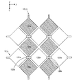
- FIG. 1 is a schematic configuration diagram of a touch panel according to an embodiment.
- FIG. 2 is an enlarged plan view of a part of the touch panel shown in FIG.
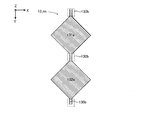
- FIG. 3 is a plan view showing connection portions of electrode portions arranged in the Y-axis direction shown in FIG.
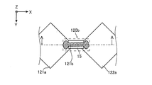
- FIG. 4 is a plan view showing connection portions of electrode portions arranged in the X-axis direction shown in FIG.
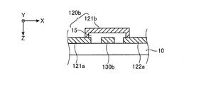
- FIG. 5 is a cross-sectional view schematically showing the AA cross section in FIG. 6A is an enlarged plan view of a connection portion of the electrode portion shown in FIG. 6B is a diagram illustrating a print pattern of the bridge wiring portion illustrated in FIG. 6A.
- FIG. 6C is a comparative example, and is a diagram illustrating a connection portion of the electrode portion when the hydrophilic treatment is not performed.
- FIG. 7 is a schematic diagram showing a display panel on which the touch panel shown in FIG. 1 is arranged.
- FIG. 8A is a cross-sectional view schematically showing a cross section of the touch panel shown in FIG.
- FIG. 8B is a cross-sectional view schematically showing a cross section of the touch panel shown in FIG. 1 after forming an insulating film.
- FIG. 8C is a cross-sectional view schematically showing a cross section of the touch panel shown in FIG. 1 after the bridge wiring portion is formed.
- FIG. 8D is a cross-sectional view schematically showing a cross section of the touch panel shown in FIG. 1 after the wiring portion is formed.
- a conductive film is formed on a substrate, a plurality of first conductive elements that are spaced apart from each other along a first direction of the substrate, and the first A first conductive part integrally formed with a first bridge wiring part that connects between the first conductive elements adjacent to each other in a direction, and the first bridge wiring part between the first conductive part and the first conductive part Forming a plurality of second conductive elements disposed along a second direction intersecting the first direction; and covering the first bridge wiring portion and adjacent to the second direction.
- the touch panel manufacturing method forms a first conductive portion and a plurality of second conductive elements on a substrate by a forming step.
- the first conductive portion includes a plurality of first conductive elements that are spaced apart along the first direction of the substrate, and a first bridge wiring portion that connects between the first conductive elements adjacent in the first direction.
- the second conductive element is formed along a second direction that intersects the first direction so as to be separated from each other with the first bridge wiring portion interposed therebetween.
- the space between the second conductive element and the second conductive element adjacent to each other in the second direction including the first bridge wiring portion is covered with the insulating film.
- a second bridge wiring portion printed using a conductive liquid material is formed by the printing process, and the second bridge wiring portion covers the insulating film between the second conductive elements adjacent in the second direction.
- the second conductive elements are connected to each other.
- the hydrophilization step at least a partial region on the surface of the second conductive element is hydrophilized. This partial region is a region where the second bridge wiring portion is formed in the second conductive element.
- the second bridge wiring portion contacting the surface of the second conductive element is more than the other portion.
- it is easy to spread on the second conductive element and the contact area with the second conductive element is increased.
- the contact resistance between the second conductive element and the second bridge wiring portion can be reduced, and the electrical conductivity of the second conductive element can be improved.
- the second configuration may be that in the first configuration, the hydrophilic treatment is a process of irradiating plasma on the surface of the second conductive element.
- the part irradiated with the plasma in the surface of the 2nd conductive element can be improved into hydrophilicity, and adhesiveness can be improved.
- the portion of the second bridge wiring portion that comes into contact with the second conductive element can be easily spread on the second conductive element, and the second conductive element and the second bridge wiring can be brought into close contact with each other.
- the third configuration may be that in the first configuration, the hydrophilic treatment is a process of irradiating the surface of the second conductive element with ultraviolet rays.
- the ultraviolet irradiation can be performed in the air by a dry process.
- it is possible to improve the adhesion by modifying the part that has been subjected to a hydrophilic treatment to hydrophilicity.
- the portion of the second bridge wiring portion that comes into contact with the second conductive element can be easily spread on the second conductive element, and the second conductive element and the second bridge wiring can be brought into close contact with each other.
- the insulating film forming step may form the insulating film using a hydrophobic material. According to the fourth configuration, since the insulating film is formed using a hydrophobic material, the second bridge wiring portion can be hardly spread on the insulating film.
- the fifth configuration may be that in the fourth configuration, the material is an acrylic resin or a polyimide resin.
- the sixth structure may be the fourth or fifth structure, wherein the insulating film forming step forms the insulating film by printing using the material. According to the sixth configuration, since the insulating film is formed by printing, manufacturing cost and time can be reduced as compared with the case where the insulating film is formed using a photomask.
- the conductive liquid material contains a conductive polymer, and the printing step is performed by spraying the conductive liquid material. It is good also as printing the 2nd bridge wiring part.
- the second bridge wiring portion is printed by spraying a conductive liquid material. Therefore, the second bridge wiring portion can be easily formed as compared with screen printing in which it is necessary to appropriately adjust the condition setting such as pressure applied to the substrate depending on the environment in which the substrate is arranged.
- An eighth configuration includes the first conductive portion, the second conductive element, and the second bridge wiring portion in any one of the first to seventh configurations, using a conductive material after the printing step.
- a wiring pattern printing step of printing a wiring pattern of wiring connected to at least one of the second conductive parts may be further included. According to the eighth configuration, since the wiring pattern of the wiring connected to at least one of the first conductive portion and the second conductive portion is formed by printing, the manufacturing cost and time are compared with the case of forming using a photomask. Can be reduced.
- FIG. 1 is a schematic configuration diagram of a touch panel according to the present embodiment.
- FIG. 1 shows a plan view of the touch panel 1.
- FIG. 2 is an enlarged plan view of a part of the touch panel 1 shown in FIG.
- the touch panel 1 includes a substrate 10, a conductive part 12 that is an example of a second conductive part, a conductive part 13 that is an example of a first conductive part, and a wiring part 14.
- the substrate 10 has a substantially rectangular shape and is made of an insulating and permeable material.
- the material of the substrate 10 is, for example, a colorless and transparent resin, glass, plastic, PET (polyethylene terephthalate) or the like.
- the conductive part 13 has M rows (M is a natural number) of conductive parts 13_1 to 13_M arranged in the X-axis direction on the substrate 10.
- each of the conductive portions 13_1 to 13_M is connected as a sense electrode to a touch panel detection circuit (not shown).
- Current values or voltage values generated in the conductive portions 13_1 to 13_M are read by the detection circuit, and changes in the electric field between the conductive portions 12_1 to 12_N and the conductive portions 13_1 to 13_M described later are detected.
- the conductive portion 13_m (m; natural number, 1 ⁇ m ⁇ M) includes a plurality of first conductive elements spaced apart along the first direction of the substrate 10 and the first conductive adjacent in the first direction. And a first bridge wiring portion for connecting the elements.
- the first conductive element is a plurality of electrode portions 131 a, 132 a, 133 a... Provided along the Y-axis direction of the substrate 10.
- electrode parts 130a when these electrode parts are not distinguished, they are referred to as electrode parts 130a.
- FIG. 3 is an enlarged plan view of a connection portion between the electrode portion 131a and the electrode portion 132a.
- the first bridge wiring portion is a bridge wiring portion 130b that connects between the electrode portion 131a and the electrode portion 132a.
- the electrode part 131a and the electrode part 132a are integrally formed with the bridge wiring part 130b. In this way, each electrode portion 130a in the conductive portion 13_m is formed integrally with the bridge wiring portion 130b that connects the adjacent electrode portions 130a.
- the electrode part 130a and the bridge wiring part 130b are formed of a transparent conductive film such as ITO (Indium Tin Oxide).
- the sheet resistance of the conductive portion 13_m including the electrode portion 130a and the bridge wiring portion 130b is preferably 10 ⁇ / ⁇ or more and 200 ⁇ / ⁇ or less, and in this example, is 100 ⁇ / ⁇ .
- the conductive portion 12 has N rows (N is a natural number) of conductive portions 12_1 to 12_N arranged in the Y-axis direction on the substrate 10 in FIG.
- each of the conductive portions 12_1 to 12_N is connected to a drive circuit (not shown) of the touch panel as a drive electrode, and is sequentially driven by drive pulses from the drive circuit.
- the conductive portion 12 ⁇ / b> _n (n: natural number, 1 ⁇ n ⁇ N) includes a plurality of second conductive elements that are spaced apart from each other along a second direction that intersects the first direction of the substrate 10.
- the second conductive elements are electrode portions 121 a, 122 a, 123 a... Arranged along the X-axis direction of the substrate 10.
- the conductive portion 12 ⁇ / b> _n includes a plurality of connection portions 120 b that connect the electrode portions 120 a adjacent in the X-axis direction.
- FIG. 4 is an enlarged plan view of the connecting portion 120b
- FIG. 5 is a cross-sectional view taken along line AA in FIG.
- a bridge wiring portion 130b of the conductive portion 13_m is formed between the electrode portions 121a and 122a.
- the connecting portion 120b is formed on the electrode portion 121a and the electrode portion 122a and the bridge wiring portion 130b so as to straddle between the electrode portion 121a and the electrode portion 122a.
- the connection part 120b includes an insulating film 15 and a bridge wiring part 121b.
- the insulating film 15 is formed on the electrode part 121a and the electrode part 122a and the bridge wiring part 130b so as to straddle between the electrode part 121a and the electrode part 122a.
- the bridge wiring part 121b is formed on the electrode part 121a, the electrode part 122a, and the insulating film 15 so as to straddle between the electrode part 121a and the electrode part 122a on the surfaces of the electrode part 121a and the electrode part 122a. That is, the electrode part 121a and the electrode part 122a are connected by the bridge wiring part 121b through the insulating film 15.
- the electrode part 120a is formed of a transparent conductive film such as ITO.
- the sheet resistance of the electrode part 120a is preferably 10 ⁇ / ⁇ or more and 200 ⁇ / ⁇ or less, and in this example, is 100 ⁇ / ⁇ .
- On the surface of the electrode portion 120a at least a portion where the bridge wiring portion 121b is formed is subjected to a hydrophilic treatment.
- the hydrophilization treatment is, for example, a treatment for irradiating the surface of the electrode part 120a with plasma or ultraviolet rays to modify the surface of the electrode part 120a to be hydrophilic.
- the adhesiveness of the surface of the electrode part 120a improves by this hydrophilic treatment.
- the insulating film 15 is formed of an organic insulating material having a dielectric constant of 4 or less and having transparency and hydrophobicity, such as polyimide resin or acrylic resin.
- the film thickness of the insulating film 15 is preferably 0.5 ⁇ m or more and 2.0 ⁇ m or less, and in this example, it is 1.5 ⁇ m. Further, the hydrophobicity of the insulating film 15 may be improved by fluorinating the surface of the insulating film 15.
- the bridge wiring part 121b is formed on the insulating film 15 and the electrode part 120a by printing using a conductive liquid material.
- the conductive liquid material contains a conductive polymer such as polyacetylene or polythiophene.
- the sheet resistance of the bridge wiring part 121b is preferably 50 ⁇ / ⁇ or more and 200 ⁇ / ⁇ or less, and in this example, is 100 ⁇ / ⁇ .
- the width in the Y-axis direction of the bridge wiring portion 121b on the insulating film 15 is Wy1
- the maximum width in the Y-axis direction of both end portions 1211 and 1212 in contact with the electrode portion 121a and the electrode portion 122a is Wy2 (W2> W1).
- Wy1 is about 0.1 mm
- Wy2 is about 0.3 mm.
- FIG. 6B is a plan view showing a print pattern of the bridge wiring portion 121b.
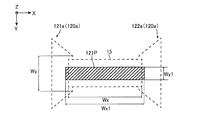
- the print pattern 121P has a width in the Y-axis direction of Wy1, and the width Wx1 in the X-axis direction has a rectangular shape longer than the width Wx of the insulating film 15. In this example, the width Wx is about 0.3 mm.
- the width Wy2 of both ends 1211 and 1212 of the bridge wiring portion 121b is substantially equal to the width Wy of the side to which the bridge wiring portion 121b is connected. In this example, the width Wy is about 0.3 mm.
- the width Wy2 of both ends 1211 and 1212 of the bridge wiring part 121b is preferably the same value as the width Wy, but may be a value larger than the width Wy1 of the bridge wiring part 121b on the insulating film 15.
- both ends of the printed bridge wiring part 121b do not spread on the electrode part 120a.
- the width Wy2 at both ends of the bridge wiring portion 121b is substantially equal to the width Wy1 of the bridge wiring portion 121b on the insulating film 15, and the bridge wiring portion 121b and the electrode The contact area with the portion 120a is smaller than that in FIG. 6A.
- a region 120S in the electrode portion 120a indicates a region contributing to electrical conduction with the bridge wiring portion 121b in the electrode portion 120a, and a shaded region 120R outside the region 120S indicates The area
- the electrode portion 120a and the bridge wiring The contact area with the part 121b increases, and the electrical conductivity in the electrode part 120a increases.
- the wiring part 14 is connected to the conductive part 12. Further, as described above, the wiring section 14 is connected to a touch panel drive circuit (not shown).
- the wiring part 14 is formed using, for example, a metal film such as aluminum or a dispersion of metal nanoparticles such as silver as a conductive material.
- the sheet resistance of the wiring part 14 is preferably 0.3 ⁇ / ⁇ or less.
- the sheet resistance of the wiring part 14 is preferably 100 ⁇ / ⁇ or more and 200 ⁇ / ⁇ or less.
- 1 illustrates the wiring portion 14 that connects the conductive portion 12 and the touch panel drive circuit (not shown), the wiring that connects the conductive portion 13 and the touch panel detection circuit (not shown) is the wiring portion.
- the same material as 14 may be used.
- the touch panel 1 is provided on a display panel 2 such as a liquid crystal panel, for example, as shown in FIG.
- the display panel 2 includes a counter substrate 21 and an active matrix substrate 22.
- a liquid crystal layer (not shown) is sealed between the counter substrate 21 and the active matrix substrate 22.
- Polarizers (not shown) are provided on the upper surface (Z-axis negative direction) of the touch panel 1 and the lower surface (Z-axis positive direction) of the active matrix substrate 22.
- gate lines and source lines are formed (both not shown), and pixels defined by the gate lines and source lines are formed.
- the counter substrate 21 includes R (red), G (green), and B (blue) color filters (not shown), and each color filter is provided corresponding to a pixel formed on the active matrix substrate 22. It is done.
- a glass substrate is used as the substrate 10 of the touch panel 1, and each manufacturing process shown below is performed in a state where the substrate 10 is disposed on the display panel 2 as illustrated in FIG. 7.
- An example of each manufacturing process will be described below with reference to FIGS. 8A to 8D.
- 8A to 8D show cross sections cut along line II shown in FIG. 1 in each manufacturing process.
- An amorphous ITO film is formed on the substrate 10 and etched using a predetermined photomask.
- the conductive portion 12 having a plurality of electrode portions 120a arranged along the X-axis direction on the substrate 10 is formed.
- a plurality of electrode portions 130a are arranged along the Y-axis direction on the substrate 10 and electrode portions 130a (see FIGS. 1 and 2) adjacent in the Y-axis direction.
- the conductive portion 13 is integrally formed with the bridge wiring portion 130b connecting the reference.
- the surface of the conductive portion 12 (electrode portion 120a) shown in FIG. 8A is irradiated with plasma to perform a hydrophilic treatment.
- the surface of the conductive part 12 (electrode part 120a) is modified to be hydrophilic.
- a pattern in which the resist is removed only in a region where the bridge wiring portion 121b is formed is formed on the conductive portion 12 illustrated in FIG. 8A by using a photolithography technique, and the bridge wiring portion 121b is formed by irradiating plasma. Only the portion to be formed may be modified to be hydrophilic.
- a predetermined printing pattern is printed on the surface of the conductive portion 12 (electrode portion 120a) by an ink jet method using a liquid material containing a polyimide resin.
- the insulating film 15 is formed on the bridge wiring portion 130b and the electrode portion 120a so as to straddle between the adjacent electrode portions 120a and 120a.
- the insulating film 15 is also formed on the electrode portion 120 a (121 a) where the wiring portion 14 is formed and on the substrate 10.
- a rectangular printed pattern 121P (see FIG. 6B) straddling between the electrode portions 120a adjacent to each other in the X-axis direction of the substrate 10 is formed on the insulating film 15 by using an ink jet method using a liquid material containing a conductive polymer. It prints on the electrode part 120a and performs a predetermined baking process.
- a bridge wiring portion 121b is formed on the insulating film 15 and the electrode portion 120a so as to straddle between the adjacent electrode portions 120a, and the adjacent electrode portions 120a and 120a are Are electrically connected through the insulating film 15.
- the bridge wiring portion 121b on the insulating film 15 after baking does not expand on the insulating film 15 due to the hydrophobicity of the insulating film 15, and the width of the bridge wiring portion 121b in the Y-axis direction is substantially equal to the width Wy1 of the printed pattern 121P. Same width. Further, the bridge wiring part 121b on the electrode part 120a after firing spreads on the electrode part 120a according to the hydrophilicity of the electrode part 120a, and the width of the bridge wiring part 121b in the Y-axis direction is the width Wy1 of the print pattern 121P. The width Wy2 is larger than that (see FIG. 6A).
- a predetermined printing pattern is printed on the electrode portion 120a (121a) and the insulating film 15 by an inkjet method using a dispersion liquid of metal nanoparticles such as silver. 8D, the wiring part 14 is formed on the electrode part 120a (121a) and the insulating film 15, and the electrode part 120a (121a) and the touch panel drive circuit (not shown) connect the wiring part 14. Connected through.
- the above is an example of a method for manufacturing the touch panel 1 according to the present embodiment.
- the portion of the electrode portion 120a where the bridge wiring portion 121b is formed is not subjected to hydrophilic treatment, and is the same as the bridge wiring portion 121b shown in FIG. 6A. It is also conceivable to print a print pattern of the shape. However, in this case, the position of the print pattern must be adjusted so that the portions of both ends 1211 and 1212 of the bridge wiring part 121b are printed at the position where the bridge wiring part 121b is connected in the electrode part 120a.
- both ends of the bridge wiring part 121b naturally spread on the electrode part 120a according to the hydrophilicity of the electrode part 120a.
- the accuracy of aligning the position of the print pattern 121P may be low.
- the bridge wiring part 121b since the hydrophilic treatment is made
- the insulating film 15 is formed of a hydrophobic material, the bridge wiring portion 121b can be prevented from spreading on the insulating film 15.
- the insulating film 15, the bridge wiring part 121b, and the wiring part 14 are formed by printing. Therefore, by performing etching using each photomask, the manufacturing cost and manufacturing process of the touch panel 1 can be reduced as compared with the case where the insulating film 15, the bridge wiring part 121b, and the wiring part 14 are formed. Moreover, in the said embodiment, since the board
- the printing patterns of the insulating film 15, the bridge wiring part 121 b, and the wiring part 14 are printed by the ink jet method, so that it depends on the environment in which the substrate 10 is arranged as compared with the case of performing screen printing. And can be printed easily.
- the example in which the insulating film 15 and the wiring part 14 are formed by printing has been described.
- one of the insulating film 15 and the wiring part 14 is formed by printing, and the other is used as a photomask. It may be formed by using and etching. Further, both the insulating film 15 and the wiring portion 14 may be formed by etching using a photomask.
- a display device with a touch panel may be realized by combining the touch panel 1 with the display panel 2 and a display panel driving unit that drives the display panel 2.
- an on-cell type touch panel in which the touch panel 1 is disposed on the display panel 2 is illustrated. May be provided on the upper portion of each display panel.
- the present invention can be used for manufacturing a display device with a touch panel, for example.
Landscapes
- Engineering & Computer Science (AREA)
- General Engineering & Computer Science (AREA)
- Theoretical Computer Science (AREA)
- Human Computer Interaction (AREA)
- Physics & Mathematics (AREA)
- General Physics & Mathematics (AREA)
- Position Input By Displaying (AREA)
Abstract
本発明は、印刷によってブリッジ配線を形成する場合に、導電素子とブリッジ配線の間の接触抵抗を低減しうるタッチパネル製造方法を提供する。基板に導電膜を成膜して第1導電部と第2導電素子(120a)とを形成する。第1導電部は、基板の第1の方向に沿って配置された複数の第1導電素子と、第1導電素子間を接続する第1ブリッジ配線部とが一体形成されている。第2導電素子は、第1ブリッジ配線部を間に挟んで離間するように第2の方向に沿って配置されている。第2導電素子の間を跨ぐように絶縁膜(15)を形成し、第2導電素子の間を接続する第2ブリッジ配線部(121b)を絶縁膜上に印刷する。第2導電素子の少なくとも第2ブリッジ配線部が形成される部分に親水化処理を行う。印刷後の第2導電素子上の第2ブリッジ配線部は、第2導電素子の親水性に応じて広がり、第2導電素子と第2ブリッジ配線部の接触抵抗が低減される。
Description
本発明は、印刷を用いたタッチパネルの製造方法に関する。
近年、スマートフォンやタブレット端末等の様々な装置に、投影型静電容量式タッチパネルが搭載されている。投影型静電容量式タッチパネルは、複数のドライブ電極が設けられたドライブラインと、ドライブラインに交差する複数のセンス電極が設けられたセンスラインとを有する。ドライブラインの複数のドライブ電極を順次駆動し、ドライブ電極とセンス電極の間の静電容量の変化を検出することにより、利用者の指やタッチペンが接触した位置を検出することができる。
タッチパネルにおけるドライブ電極とセンス電極を含む導電部や配線等を印刷によって形成する技術が知られている。例えば、特開2010-146283号公報には、基板に、X軸方向に配列された第1導電素子と、隣接するX軸方向の第1導電素子どうしを接続する第1導電配線部と、Y軸方向に配列された第2導電素子とが形成され、隣接するY軸方向の第2導電素子どうしを接続する第2導電配線部を、ナノ粒子分散液を用いて印刷する技術が開示されている。また、特開2010-146785号公報には、絶縁基板上に、スクリーン印刷やインクジェット印刷等により高分子材料を塗布することにより、透明導電膜からなるy方向電極とx方向電極を形成する技術が開示されている。特開2010-211647号公報には、X軸方向とY軸方向に規則的に配置された面状電極を有する電極パターンが形成されたタッチパネル基板が開示されている。この電極パターンは、隣接するY軸方向の面状電極どうしを接続する上部配線とY軸方向の面状電極とが一体的に形成され、X軸方向の面状電極どうしは、導電性の液状材料を用いたインクジェット法等の液層成膜法で形成された下部配線で接続されている。
基板上のX軸又はY軸方向に配列された導電素子の間を接続するブリッジ配線が導電素子と接触する面積は導電素子における電気伝導率に影響する。印刷によってブリッジ配線が形成される場合、印刷後のブリッジ配線と導電素子との間の接触面積が小さくなるほど、導電素子とブリッジ配線の間の接触抵抗が大きくなり、導電素子における電気伝導率が低下する。
本発明は、印刷によってブリッジ配線を形成する場合に、導電素子とブリッジ配線の間の接触抵抗を低減しうるタッチパネル製造方法を提供することを目的とする。
第1の発明に係るタッチパネル製造方法は、基板に導電膜を成膜し、前記基板の第1の方向に沿って離間して配置された複数の第1導電素子と、前記第1の方向に隣接する前記第1導電素子の間を接続する第1ブリッジ配線部とが一体的に形成された第1導電部と、前記第1ブリッジ配線部を間に挟んで離間するように、前記第1の方向と交差する第2の方向に沿って配置された複数の第2導電素子とを形成する形成工程と、前記第1ブリッジ配線部を覆い、前記第2の方向に隣接する前記第2導電素子の間を跨ぐように絶縁膜を形成する絶縁膜形成工程と、導電性の液状材料を用い、前記第2の方向に隣接する前記第2導電素子の間を接続する第2ブリッジ配線部を、前記絶縁膜の上に印刷する印刷工程と、を含むタッチパネル製造方法であって、前記第2導電素子の表面において、少なくとも前記第2ブリッジ配線部が形成される部分に、親水化処理を行う親水化工程をさらに含む。
第2の発明は、第1の発明において、前記親水化処理は、前記第2導電素子の表面にプラズマを照射する処理である。
第3の発明は、第1の発明において、前記親水化処理は、前記第2導電素子の表面に紫外線を照射する処理である。
第4の発明は、第1から第3のいずれかの発明において、前記絶縁膜形成工程は、疎水性を有する材料を用いて前記絶縁膜を形成する。
第5の発明は、第4の発明において、前記材料は、アクリル系樹脂、又はポリイミド樹脂である。
第6の発明は、第4又は第5の発明において、前記絶縁膜形成工程は、前記材料を用いた印刷によって前記絶縁膜を形成する。
第7の発明は、第1から第6のいずれかの発明において、前記導電性の液状材料は、導電性ポリマーを含有し、前記印刷工程は、前記導電性の液状材料を噴霧することにより前記第2ブリッジ配線部を印刷する。
第8の発明は、第1から第7のいずれかの発明において、前記印刷工程後、導電性材料を用い、前記第1導電部と、前記第2導電素子及び前記第2ブリッジ配線部を含む第2導電部の少なくとも一方と接続する配線の配線パターンを印刷する配線パターン印刷工程をさらに含む。
本発明の構成によれば、印刷によってブリッジ配線を形成する場合に、導電素子とブリッジ配線の間の接触抵抗を低減することができる。
本発明の一実施形態に係るタッチパネル製造方法は、基板に導電膜を成膜し、前記基板の第1の方向に沿って離間して配置された複数の第1導電素子と、前記第1の方向に隣接する前記第1導電素子の間を接続する第1ブリッジ配線部とが一体的に形成された第1導電部と、前記第1ブリッジ配線部を間に挟んで離間するように、前記第1の方向と交差する第2の方向に沿って配置された複数の第2導電素子とを形成する形成工程と、前記第1ブリッジ配線部を覆い、前記第2の方向に隣接する前記第2導電素子の間を跨ぐように絶縁膜を形成する絶縁膜形成工程と、導電性の液状材料を用い、前記第2の方向に隣接する前記第2導電素子の間を接続する第2ブリッジ配線部を、前記絶縁膜の上に印刷する印刷工程と、を含むタッチパネル製造方法であって、前記第2導電素子の表面において、少なくとも前記第2ブリッジ配線部が形成される部分に、親水化処理を行う親水化工程をさらに含む(第1の構成)。
第1の構成に係るタッチパネル製造方法は、形成工程により、基板に第1導電部と複数の第2導電素子とを形成する。第1導電部は、基板の第1の方向に沿って離間して配置された複数の第1導電素子と、第1の方向に隣接する第1導電素子間を接続する第1ブリッジ配線部とが一体となって形成される。第2導電素子は、第1ブリッジ配線部を挟んで離間するように、第1の方向に交差する第2の方向に沿って形成される。絶縁膜形成工程により、第1ブリッジ配線部を含む、第2の方向に隣接する第2導電素子と第2導電素子との間が絶縁膜で覆われる。印刷工程により、導電性の液状材料を用いて印刷された第2ブリッジ配線部が形成され、第2ブリッジ配線部によって、第2の方向に隣接する第2導電素子の間における絶縁膜を覆うように第2導電素子の間が接続される。親水化工程により、第2導電素子の表面における少なくとも一部領域に親水化処理がなされる。この一部領域は、第2導電素子において第2ブリッジ配線部が形成される領域である。
第2導電素子の表面において、少なくとも第2ブリッジ配線部が形成される部分に、親水化処理がなされているため、第2導電素子の表面に接触する第2ブリッジ配線部は、他の部分よりも第2導電素子上で広がりやすくなり、第2導電素子との接触面積が大きくなる。その結果、第2導電素子と第2ブリッジ配線部の間の接触抵抗を低下させることができ、第2導電素子における電気伝導率を向上させることができる。
第2の構成は、第1の構成において、前記親水化処理は、前記第2導電素子の表面にプラズマを照射する処理である、こととしてもよい。第2の構成によれば、第2導電素子の表面においてプラズマが照射された部分を親水性に改質して接着性を向上させることができる。その結果、第2導電素子に接触する第2ブリッジ配線部の部分が第2導電素子上で広がりやすくなることに加え、第2導電素子と第2ブリッジ配線とを密着させることができる。
第3の構成は、第1の構成において、前記親水化処理は、前記第2導電素子の表面に紫外線を照射する処理である、こととしてもよい。第3の構成によれば、紫外線の照射は、ドライプロセスで、大気中で行うことができる。また、親水化処理がなされた部分を親水性に改質して接着性を向上させることができる。その結果、第2導電素子に接触する第2ブリッジ配線部の部分が第2導電素子上で広がりやすくなることに加え、第2導電素子と第2ブリッジ配線とを密着させることができる。
第4の構成は、第1から第3のいずれかの構成において、前記絶縁膜形成工程は、疎水性を有する材料を用いて前記絶縁膜を形成する、こととしてもよい。第4の構成によれば、絶縁膜は疎水性を有する材料を用いて形成されるため、絶縁膜上では第2ブリッジ配線部を広がりにくくすることができる。
第5の構成は、第4の構成において、前記材料は、アクリル系樹脂、又はポリイミド樹脂である、こととしてもよい。
第6の構成は、第4又は第5の構成において、前記絶縁膜形成工程は、前記材料を用いた印刷によって前記絶縁膜を形成する、こととしてもよい。第6の構成によれば、絶縁膜を印刷により形成するため、フォトマスクを用いて形成する場合と比べ、製造コスト及び時間を低減することができる。
第7の構成は、第1から第6のいずれかの構成において、前記導電性の液状材料は、導電性ポリマーを含有し、前記印刷工程は、前記導電性の液状材料を噴霧することにより前記第2ブリッジ配線部を印刷する、こととしてもよい。第7の構成によれば、導電性の液状材料を噴霧して第2ブリッジ配線部を印刷する。そのため、基板が配置される環境によって、基板に加える圧力等の条件設定を適宜調整する必要があるスクリーン印刷と比べ、第2ブリッジ配線部を容易に形成することができる。
第8の構成は、第1から第7のいずれかの構成において、前記印刷工程後、導電性材料を用い、前記第1導電部と、前記第2導電素子及び前記第2ブリッジ配線部を含む第2導電部の少なくとも一方と接続する配線の配線パターンを印刷する配線パターン印刷工程をさらに含む、こととしてもよい。第8の構成によれば、印刷により、第1導電部と第2導電部の少なくとも一方と接続する配線の配線パターンを形成するため、フォトマスクを用いて形成する場合と比べ、製造コスト及び時間を低減することができる。
以下、図面を参照し、本発明の実施の形態を詳しく説明する。図中同一又は相当部分には同一符号を付してその説明は繰り返さない。
図1は、本実施形態に係るタッチパネルの概略構成図である。図1は、タッチパネル1の平面図を示している。また、図2は、図1に示すタッチパネル1の一部を拡大した平面図である。
図1に示すように、タッチパネル1は、基板10と、第2導電部の一例である導電部12と、第1導電部の一例である導電部13と、配線部14とを備える。
基板10は、略矩形状を有し、絶縁性及び透過性を有する材料で構成される。基板10の材料は、例えば、無色透明な樹脂、ガラス、プラスチック、PET(polyethylene terephthalate)等である。
導電部13は、図1に示すように、基板10上のX軸方向に配列されたM列(Mは自然数)の導電部13_1~13_Mを有する。本実施形態において、導電部13_1~13_Mの各々は、センス電極としてタッチパネルの検出回路(図示略)に接続される。導電部13_1~13_Mにおいて発生する電流値又は電圧値が検出回路で読み取られ、後述の導電部12_1~12_Nと導電部13_1~13_Mの間の電界の変化が検出される。
導電部13_m(m;自然数、1≦m≦M)は、基板10の第1の方向に沿って離間して配置された複数の第1導電素子と、第1の方向に隣接する第1導電素子の間を接続する第1ブリッジ配線部とを有する。図2の例において、第1導電素子は、基板10のY軸方向に沿って複数設けられた電極部131a,132a,133a…である。以下、これら電極部を区別しないときは、電極部130aと称する。
図3は、電極部131aと電極部132aとの接続部分を拡大した平面図である。図3の例において、第1ブリッジ配線部は、電極部131aと電極部132aの間を接続するブリッジ配線部130bである。電極部131aと電極部132aは、ブリッジ配線部130bと一体形成されている。このように、導電部13_mにおける各電極部130aは、隣接する電極部130aの間を接続するブリッジ配線部130bと一体となって形成されている。
電極部130aとブリッジ配線部130bは、ITO(Indium Tin Oxide)等の透明導電膜で形成されている。電極部130aとブリッジ配線部130bを含む導電部13_mのシート抵抗は、10Ω/□以上、200Ω/□以下が好ましく、この例では、100Ω/□となっている。
導電部12は、図1において、基板10上のY軸方向に配列されたN行(Nは自然数)の導電部12_1~12_Nを有する。本実施形態において、導電部12_1~12_Nの各々は、ドライブ電極としてタッチパネルの駆動回路(図示略)に接続され、駆動回路からの駆動パルスによって順次駆動される。
導電部12_n(n:自然数、1≦n≦N)は、基板10の第1の方向に交差する第2の方向に沿って離間して配置された複数の第2導電素子を有する。図2の例において、第2導電素子は、基板10のX軸方向に沿って配置された電極部121a,122a,123a…である。なお、以下、これら電極部を区別しないときは、電極部120aと称する。また、図2に示すように、導電部12_nは、X軸方向に隣接する電極部120aの間を接続する複数の接続部120bを有する。
図4は、接続部120bの部分を拡大した平面図であり、図5は、図4におけるA-A線で切断した断面図である。なお、便宜上、図4において図示を省略するが、電極部121a,122aの間には、導電部13_mのブリッジ配線部130bが形成されている。図4及び図5に示すように、接続部120bは、電極部121a及び電極部122aの間を跨ぐように、電極部121a及び電極部122aと、ブリッジ配線部130bの上に形成されている。
接続部120bは、絶縁膜15とブリッジ配線部121bとを含む。絶縁膜15は、電極部121aと電極部122aの間を跨ぐように、電極部121a及び電極部122aと、ブリッジ配線部130bの上に形成されている。ブリッジ配線部121bは、電極部121aと電極部122aの表面において、電極部121aと電極部122aの間を跨ぐように、電極部121a及び電極部122aと絶縁膜15の上に形成されている。つまり、電極部121aと電極部122aは、絶縁膜15を介してブリッジ配線部121bによって接続されている。
電極部120aは、ITO等の透明導電膜で形成されている。電極部120aのシート抵抗は、10Ω/□以上、200Ω/□以下が好ましく、この例では、100Ω/□となっている。電極部120aの表面において、少なくともブリッジ配線部121bが形成される部分には、親水化処理がなされている。親水化処理は、例えば、電極部120aの表面にプラズマ又は紫外線を照射し、電極部120aの表面を親水性に改質する処理である。また、この親水化処理により、電極部120aの表面の接着性が向上する。
絶縁膜15は、例えば、ポリイミド樹脂又はアクリル系樹脂等、誘電率が4以下で、透過性及び疎水性を有する有機絶縁材料で形成されている。絶縁膜15の膜厚は、0.5μm以上、2.0μm以下が好ましく、この例では、1.5μmとなっている。また、絶縁膜15の表面をフッ素化処理することにより、絶縁膜15の疎水性を向上させてもよい。
ブリッジ配線部121bは、導電性の液状材料を用いた印刷によって、絶縁膜15及び電極部120aの上に形成される。本実施形態では、導電性の液状材料は、例えば、ポリアセチレン又はポリチオフェン等の導電性ポリマーを含有する。また、ブリッジ配線部121bのシート抵抗は、50Ω/□以上、200Ω/□以下が好ましく、この例では、100Ω/□となっている。
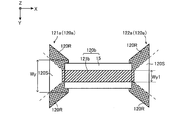
ここで、図6Aに接続部120bを拡大した模式図を示す。図6Aに示すように、絶縁膜15上のブリッジ配線部121bのY軸方向の幅はWy1であり、電極部121aと電極部122aに接触する両端部分1211,1212のY軸方向の最大幅はWy2(W2>W1)である。この例において、Wy1は約0.1mmであり、Wy2は約0.3mmである。
上記したように、ブリッジ配線部121bは、導電性の液状材料を用いた印刷によって絶縁膜15及び電極部120aの上に形成される。図6Bは、ブリッジ配線部121bの印刷パターンを示す平面図である。図6Bに示すように、印刷パターン121Pは、Y軸方向の幅がWy1であり、X軸方向の幅Wx1は、絶縁膜15のその幅Wxよりも長い矩形状を有する。この例において、幅Wxは、約0.3mmである。
電極部120aにおいて、ブリッジ配線部121bが接触する部分は親水化されているため、その部分におけるブリッジ配線部121bの接触角は、親水化処理がなされていない部分よりも小さくなる。その結果、図6Aに示すように、印刷後のブリッジ配線部121bの両端1211,1212は電極部120aの上で広がり、両端1211,1212の幅は、絶縁膜15上のブリッジ配線部121bの幅Wy1より大きくなる。この例では、ブリッジ配線部121bの両端1211,1212の幅Wy2は、ブリッジ配線部121bが接続される辺の幅Wyと略同等の長さとなっている。この例において、幅Wyは、約0.3mmである。
なお、ブリッジ配線部121bの両端1211,1212の幅Wy2は、幅Wyと同等の値であることが好ましいが、絶縁膜15上のブリッジ配線部121bの幅Wy1より大きい値であればよい。
一方、電極部120aにおいて、ブリッジ配線部121bが接触する部分に親水化処理を行っていない場合には、印刷後のブリッジ配線部121bの両端は電極部120aの上で広がらない。その結果、図6Cの比較例に示すように、ブリッジ配線部121bの両端の幅Wy2は、絶縁膜15上のブリッジ配線部121bの幅Wy1と略同等の長さとなり、ブリッジ配線部121bと電極部120aとの接触面積は図6Aと比べて小さくなる。
図6Aと、その比較例を示す図6Cにおいて、電極部120aにおける領域120Sは、電極部120aにおいてブリッジ配線部121bとの電気伝導に寄与する領域を示し、領域120Sより外側の網掛け領域120Rは電気伝導に寄与しない領域を示している。電極部120aとブリッジ配線部121bとの接触面積が大きいほど、電極部120aとブリッジ配線部121bとの接触抵抗が小さくなり、電極部120aにおける電気伝導率は向上する。つまり、電極部120a上のブリッジ配線部121bのY軸方向の幅Wy2の値が、ブリッジ配線部121bが接続される電極部120aの辺の幅Wyの値に近づくほど、電極部120aとブリッジ配線部121bとの接触面積が大きくなり、電極部120aにおける電気伝導率が高くなる。
従って、図6Aに示す状態、つまり、ブリッジ配線部121bが接触する電極部120aの部分に親水化処理を行った方が、親水化処理を行わない図6Cに示す状態よりも電極部120aとブリッジ配線部121bとの接触抵抗が小さくなり、電極部120aにおける電気伝導率が高くなる。
図1において、配線部14は、導電部12に接続されている。また、上記したように、配線部14は、タッチパネルの駆動回路(図示略)と接続されている。配線部14は、導電性材料として、例えば、アルミニウム等の金属膜、又は、銀等の金属ナノ粒子の分散液を用いて形成されている。配線部14がアルミニウム等の金属膜で形成されている場合、配線部14のシート抵抗は、0.3Ω/□以下が好ましい。また、配線部14が銀等の金属ナノ粒子の分散液で形成されている場合、配線部14のシート抵抗は、100Ω/□以上、200Ω/□以下が好ましい。なお、図1では、導電部12とタッチパネル駆動回路(図示略)とを接続する配線部14を例示しているが、導電部13とタッチパネル検出回路(図示略)とを接続する配線を配線部14と同じ材料を用いて形成してもよい。
タッチパネル1は、例えば、図7に示すように、液晶パネル等の表示パネル2の上に設けられる。表示パネル2は、対向基板21とアクティブマトリクス基板22とを有する。対向基板21とアクティブマトリクス基板22の間には液晶層(図示略)が封入されている。タッチパネル1の上面(Z軸負方向)と、アクティブマトリクス基板22の下面(Z軸正方向)には偏光板(図示略)が設けられる。アクティブマトリクス基板22には、ゲート線とソース線とが形成され(いずれも図示略)、ゲート線とソース線とで規定される画素が形成されている。対向基板21は、R(赤)、G(緑)、及びB(青)のカラーフィルタ(図示略)を備え、各々のカラーフィルタは、アクティブマトリクス基板22に形成された画素に対応して設けられる。
<タッチパネルの製造方法>
本実施形態では、タッチパネル1の基板10としてガラス基板を用い、図7に示すように、表示パネル2の上に基板10を配置した状態で以下に示す各製造工程を行う。以下、各製造工程の一例について、図8A~図8Dを用いて説明する。なお、図8A~図8Dは、各製造工程において、図1に示すI-I線で切断した断面を示している。
本実施形態では、タッチパネル1の基板10としてガラス基板を用い、図7に示すように、表示パネル2の上に基板10を配置した状態で以下に示す各製造工程を行う。以下、各製造工程の一例について、図8A~図8Dを用いて説明する。なお、図8A~図8Dは、各製造工程において、図1に示すI-I線で切断した断面を示している。
(導電部形成)
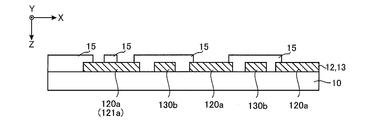
基板10上に、アモルファスITOを成膜し、所定のフォトマスクを用いてエッチングする。これにより、図8Aに示すように、基板10上のX軸方向に沿って配列された複数の電極部120aを有する導電部12が形成される。また、図8Aに示すように、基板10上のY軸方向に沿って配列された複数の電極部130a(図1,2参照)と、Y軸方向に隣接する電極部130a(図1,2参照)を接続するブリッジ配線部130bとが一体的に形成された導電部13が形成される。
基板10上に、アモルファスITOを成膜し、所定のフォトマスクを用いてエッチングする。これにより、図8Aに示すように、基板10上のX軸方向に沿って配列された複数の電極部120aを有する導電部12が形成される。また、図8Aに示すように、基板10上のY軸方向に沿って配列された複数の電極部130a(図1,2参照)と、Y軸方向に隣接する電極部130a(図1,2参照)を接続するブリッジ配線部130bとが一体的に形成された導電部13が形成される。
(親水化工程)
次に、図8Aに示す導電部12(電極部120a)の表面にプラズマを照射して親水化処理を行う。これにより、導電部12(電極部120a)の表面が親水性に改質される。なお、図8Aに示す導電部12の上に、フォトリソグラフィーの手法を用い、ブリッジ配線部121bを形成する領域のみレジストを除去したパターンを形成し、プラズマを照射することにより、ブリッジ配線部121bを形成する部分のみ親水性に改質してもよい。
次に、図8Aに示す導電部12(電極部120a)の表面にプラズマを照射して親水化処理を行う。これにより、導電部12(電極部120a)の表面が親水性に改質される。なお、図8Aに示す導電部12の上に、フォトリソグラフィーの手法を用い、ブリッジ配線部121bを形成する領域のみレジストを除去したパターンを形成し、プラズマを照射することにより、ブリッジ配線部121bを形成する部分のみ親水性に改質してもよい。
(絶縁膜形成)
次に、ポリイミド樹脂を含有する液状材料を用い、インクジェット方式により、導電部12(電極部120a)の表面に所定の印刷パターンを印刷する。これにより、図8Bに示すように、隣接する電極部120aと電極部120aの間を跨ぐように、ブリッジ配線部130b及び電極部120aの上に絶縁膜15が形成される。また、図1に示すように、配線部14が形成される電極部120a(121a)の上と、基板10の上にも絶縁膜15が形成される。
次に、ポリイミド樹脂を含有する液状材料を用い、インクジェット方式により、導電部12(電極部120a)の表面に所定の印刷パターンを印刷する。これにより、図8Bに示すように、隣接する電極部120aと電極部120aの間を跨ぐように、ブリッジ配線部130b及び電極部120aの上に絶縁膜15が形成される。また、図1に示すように、配線部14が形成される電極部120a(121a)の上と、基板10の上にも絶縁膜15が形成される。
(ブリッジ配線部121b形成)
次に、導電性ポリマーを含有する液状材料を用い、インクジェット方式により、基板10のX軸方向に隣接する電極部120aの間を跨ぐ矩形状の印刷パターン121P(図6B参照)を絶縁膜15と電極部120aの上に印刷し、所定の焼成処理を行う。
次に、導電性ポリマーを含有する液状材料を用い、インクジェット方式により、基板10のX軸方向に隣接する電極部120aの間を跨ぐ矩形状の印刷パターン121P(図6B参照)を絶縁膜15と電極部120aの上に印刷し、所定の焼成処理を行う。
これにより、図8Cに示すように、隣接する電極部120aの間を跨ぐように、絶縁膜15と電極部120aの上にブリッジ配線部121bが形成され、隣接する電極部120aと電極部120aは、絶縁膜15を介して電気的に接続される。
焼成後の絶縁膜15上のブリッジ配線部121bは、絶縁膜15の疎水性により、絶縁膜15上で広がらず、ブリッジ配線部121bのY軸方向の幅は、印刷パターン121Pの幅Wy1と略同じ幅となる。また、焼成後の電極部120a上のブリッジ配線部121bは、電極部120aの親水性に応じて電極部120a上で広がり、ブリッジ配線部121bのY軸方向の幅は、印刷パターン121Pの幅Wy1よりも大きい幅Wy2となる(図6A参照)。
(配線部形成)
ブリッジ配線部121bの形成後、銀等の金属ナノ粒子の分散液を用い、インクジェット方式により、電極部120a(121a)及び絶縁膜15の上に所定の印刷パターンを印刷する。これにより、図8Dに示すように、電極部120a(121a)及び絶縁膜15の上に配線部14が形成され、電極部120a(121a)とタッチパネル駆動回路(図示略)とが配線部14を介して接続される。以上が、本実施形態に係るタッチパネル1の製造方法の一例である。
ブリッジ配線部121bの形成後、銀等の金属ナノ粒子の分散液を用い、インクジェット方式により、電極部120a(121a)及び絶縁膜15の上に所定の印刷パターンを印刷する。これにより、図8Dに示すように、電極部120a(121a)及び絶縁膜15の上に配線部14が形成され、電極部120a(121a)とタッチパネル駆動回路(図示略)とが配線部14を介して接続される。以上が、本実施形態に係るタッチパネル1の製造方法の一例である。
ブリッジ配線部121bと電極部120aの接触面積を大きくするために、例えば、ブリッジ配線部121bが形成される電極部120aの部分に親水化処理を行わず、図6Aに示すブリッジ配線部121bと同様の形状の印刷パターンを印刷することも考えられる。しかしながら、この場合には、電極部120aにおいてブリッジ配線部121bを接続させる位置に、ブリッジ配線部121bの両端1211,1212の部分が印刷されるように印刷パターンの位置を合わせなければならない。上記実施形態では、ブリッジ配線部121bの印刷パターン121Pを印刷後、ブリッジ配線部121bの両端は、電極部120aの親水性に応じて自然に電極部120a上で広がるので、上記の場合と比べ、印刷パターン121Pの位置を合わせる精度が低くてもよい。
また、上記実施形態では、電極部120aの表面において、ブリッジ配線部121bが形成される部分に親水化処理がなされているため、電極部120a上でブリッジ配線部121bは広がりやすくなり、電極部120aとブリッジ配線部121bとの接触面積が大きくなる。その結果、電極部120aとブリッジ配線部121bの接触抵抗が低減され、電極部120aにおける電気伝導率を向上させることができる。また、絶縁膜15は、疎水性を有する材料で形成されているため、ブリッジ配線部121bが絶縁膜15上で広がらないようにすることができる。
また、上記実施形態では、絶縁膜15、ブリッジ配線部121b、及び配線部14を印刷によって形成する。そのため、各々のフォトマスクを用いてエッチングを行うことにより、絶縁膜15、ブリッジ配線部121b、及び配線部14を形成する場合と比べ、タッチパネル1の製造コスト及び製造工程を削減することができる。また、上記実施形態では、液晶層が封入された表示パネル2の上に基板10が配置されているため、スクリーン印刷によって絶縁膜15、ブリッジ配線部121b、及び配線部14を形成する場合には、基板10に加える圧力等の条件を調整しなければならない。上記実施形態では、インクジェット方式により絶縁膜15、ブリッジ配線部121b、及び配線部14の各印刷パターンを印刷するため、スクリーン印刷を行う場合と比べ、基板10が配置される環境に左右されることなく容易に印刷することができる。
<変形例>
以上、本発明の実施の形態を説明したが、上述した実施の形態は本発明を実施するための例示に過ぎない。よって、本発明は上述した実施の形態に限定されることなく、その趣旨を逸脱しない範囲内で上述した実施の形態を適宜変形して実施することが可能である。以下、本発明の変形例について説明する。
以上、本発明の実施の形態を説明したが、上述した実施の形態は本発明を実施するための例示に過ぎない。よって、本発明は上述した実施の形態に限定されることなく、その趣旨を逸脱しない範囲内で上述した実施の形態を適宜変形して実施することが可能である。以下、本発明の変形例について説明する。
(1)上述した実施形態では、基板10のX軸方向に隣接する電極部120aの間を、絶縁膜15を介してブリッジ配線部121bで接続する例を説明したが、基板10のY軸方向に隣接する電極部130aの間を、上記実施形態と同様、絶縁膜15を介してブリッジ配線部によって接続してもよい。要は、導電部12又は導電部13において隣接する電極部の間を、絶縁膜15を介してブリッジ配線部で接続するように構成すればよい。
(2)上述した実施形態では、絶縁膜15及び配線部14を印刷によって形成する例を説明したが、絶縁膜15及び配線部14のいずれか一方を印刷によって形成し、他方を、フォトマスクを用いてエッチングすることにより形成してもよい。また、絶縁膜15及び配線部14のいずれもフォトマスクを用いてエッチングすることにより形成してもよい。
(3)上述した実施形態において、タッチパネル1に、表示パネル2及び表示パネル2を駆動する表示パネル駆動部を組み合わせ、タッチパネル付き表示装置を実現してもよい。
(4)上述したタッチパネルの製造方法の工程の実行順序は、上記記載の順序に限定されるものではなく、発明の要旨を逸脱しない範囲で適宜実行順序を入れ替えてもよい。
(5)上述した実施形態の図7では、タッチパネル1を表示パネル2の上に配置したオンセル型タッチパネルを例示したが、タッチパネル1は、対向基板21の上面とアクティブマトリクス基板22の下面に偏光板が各々配置された表示パネルの上部に設けられてもよい。
(6)上述した実施形態のタッチパネル1の製造方法では、インクジェット方式を用いた印刷により絶縁膜15、ブリッジ配線部121b、及び配線部14を形成する例を説明したが、オフセット印刷方式を用いた印刷によりこれらを形成してもよい。
本発明は、例えばタッチパネル付き表示装置の製造に利用することができる。
Claims (8)
- 基板に導電膜を成膜し、前記基板の第1の方向に沿って離間して配置された複数の第1導電素子と、前記第1の方向に隣接する前記第1導電素子の間を接続する第1ブリッジ配線部とが一体的に形成された第1導電部と、前記第1ブリッジ配線部を間に挟んで離間するように、前記第1の方向と交差する第2の方向に沿って配置された複数の第2導電素子とを形成する形成工程と、前記第1ブリッジ配線部を覆い、前記第2の方向に隣接する前記第2導電素子の間を跨ぐように絶縁膜を形成する絶縁膜形成工程と、導電性の液状材料を用い、前記第2の方向に隣接する前記第2導電素子の間を接続する第2ブリッジ配線部を、前記絶縁膜の上に印刷する印刷工程と、を含むタッチパネル製造方法であって、
前記第2導電素子の表面において、少なくとも前記第2ブリッジ配線部が形成される部分に、親水化処理を行う親水化工程をさらに含む、タッチパネル製造方法。 - 前記親水化処理は、前記第2導電素子の表面にプラズマを照射する処理である、請求項1に記載のタッチパネル製造方法。
- 前記親水化処理は、前記第2導電素子の表面に紫外線を照射する処理である、請求項1に記載のタッチパネル製造方法。
- 前記絶縁膜形成工程は、疎水性を有する材料を用いて前記絶縁膜を形成する、請求項1から3のいずれか一項に記載のタッチパネル製造方法。
- 前記材料は、アクリル系樹脂、又はポリイミド樹脂である、請求項4に記載のタッチパネル製造方法。
- 前記絶縁膜形成工程は、前記材料を用いた印刷によって前記絶縁膜を形成する、請求項4又は5に記載のタッチパネル製造方法。
- 前記導電性の液状材料は、導電性ポリマーを含有し、
前記印刷工程は、前記導電性の液状材料を噴霧することにより前記第2ブリッジ配線部を印刷する、請求項1から6のいずれか一項に記載のタッチパネル製造方法。 - 前記印刷工程後、導電性材料を用い、前記第1導電部と、前記第2導電素子及び前記第2ブリッジ配線部を含む第2導電部の少なくとも一方と接続する配線の配線パターンを印刷する配線パターン印刷工程をさらに含む、請求項1から7のいずれか一項に記載のタッチパネル製造方法。
Applications Claiming Priority (2)
| Application Number | Priority Date | Filing Date | Title |
|---|---|---|---|
| JP2013-269474 | 2013-12-26 | ||
| JP2013269474 | 2013-12-26 |
Publications (1)
| Publication Number | Publication Date |
|---|---|
| WO2015098608A1 true WO2015098608A1 (ja) | 2015-07-02 |
Family
ID=53478472
Family Applications (1)
| Application Number | Title | Priority Date | Filing Date |
|---|---|---|---|
| PCT/JP2014/083206 Ceased WO2015098608A1 (ja) | 2013-12-26 | 2014-12-16 | タッチパネル製造方法 |
Country Status (1)
| Country | Link |
|---|---|
| WO (1) | WO2015098608A1 (ja) |
Cited By (1)
| Publication number | Priority date | Publication date | Assignee | Title |
|---|---|---|---|---|
| JP2018190411A (ja) * | 2017-04-27 | 2018-11-29 | エルジー ディスプレイ カンパニー リミテッド | 表示装置及びその製造方法 |
Citations (4)
| Publication number | Priority date | Publication date | Assignee | Title |
|---|---|---|---|---|
| JP2010267223A (ja) * | 2009-05-18 | 2010-11-25 | Seiko Epson Corp | タッチパネルの製造方法及び表示装置製造方法並びに電子機器製造方法 |
| JP2011013725A (ja) * | 2009-06-30 | 2011-01-20 | Seiko Epson Corp | タッチパネル、タッチパネルの製造方法、電気光学装置、電子機器 |
| JP2012119343A (ja) * | 2009-03-31 | 2012-06-21 | Shibaura Mechatronics Corp | 太陽電池の製造方法、太陽電池の製造装置及び太陽電池 |
| WO2013146859A1 (ja) * | 2012-03-28 | 2013-10-03 | 日本写真印刷株式会社 | タッチセンサーとその製造方法、およびタッチセンサー製造用転写リボン |
-
2014
- 2014-12-16 WO PCT/JP2014/083206 patent/WO2015098608A1/ja not_active Ceased
Patent Citations (4)
| Publication number | Priority date | Publication date | Assignee | Title |
|---|---|---|---|---|
| JP2012119343A (ja) * | 2009-03-31 | 2012-06-21 | Shibaura Mechatronics Corp | 太陽電池の製造方法、太陽電池の製造装置及び太陽電池 |
| JP2010267223A (ja) * | 2009-05-18 | 2010-11-25 | Seiko Epson Corp | タッチパネルの製造方法及び表示装置製造方法並びに電子機器製造方法 |
| JP2011013725A (ja) * | 2009-06-30 | 2011-01-20 | Seiko Epson Corp | タッチパネル、タッチパネルの製造方法、電気光学装置、電子機器 |
| WO2013146859A1 (ja) * | 2012-03-28 | 2013-10-03 | 日本写真印刷株式会社 | タッチセンサーとその製造方法、およびタッチセンサー製造用転写リボン |
Cited By (2)
| Publication number | Priority date | Publication date | Assignee | Title |
|---|---|---|---|---|
| JP2018190411A (ja) * | 2017-04-27 | 2018-11-29 | エルジー ディスプレイ カンパニー リミテッド | 表示装置及びその製造方法 |
| US10719152B2 (en) | 2017-04-27 | 2020-07-21 | Lg Display Co., Ltd | Display device and method of manufacturing the same |
Similar Documents
| Publication | Publication Date | Title |
|---|---|---|
| JP5063500B2 (ja) | パネル型入力装置、パネル型入力装置の製造方法、及びパネル型入力装置を備えた電子機器 | |
| US9280013B2 (en) | Touch panel configured to reduce effects of moisture, and display apparatus provided with touch panel | |
| JP4616324B2 (ja) | タッチセンサ | |
| CN101553776B (zh) | 触摸面板装置及其制造方法 | |
| US9011703B2 (en) | Method for manufacturing touch screen panel | |
| US9229555B2 (en) | Touch screen panel and method of manufacturing the same | |
| US20170228090A1 (en) | Conductive film and touch panel sensor provided with same | |
| JP2009259063A (ja) | タッチパネルおよびその製造方法 | |
| US20100309166A1 (en) | Touch panel and display device equipped with the same | |
| JP6233075B2 (ja) | タッチパネルセンサおよびタッチパネルセンサを備える入出力装置 | |
| WO2011125281A1 (ja) | タッチパネル付き表示装置 | |
| JP5827972B2 (ja) | タッチセンサ一体型表示装置 | |
| KR20140070106A (ko) | 플렉서블 터치스크린패널 및 그 제조방법 | |
| CN108255359A (zh) | 触控面板及其制造方法 | |
| KR102335116B1 (ko) | 터치 스크린 패널 및 이의 제조 방법 | |
| JP4882016B2 (ja) | タッチセンサ | |
| US9195359B2 (en) | Providing resistance portions along touch panel electrodes, for adjusting electric potential distribution | |
| KR101878858B1 (ko) | 입력 장치 및 그의 제조 방법 | |
| WO2013008675A1 (ja) | タッチパネルおよびタッチパネル付き表示装置 | |
| KR102367248B1 (ko) | 터치 스크린 패널 | |
| KR20110112615A (ko) | 터치패널용 전극 형성 방법 | |
| US20110317115A1 (en) | Liquid crystal display device and method for manufacturing same | |
| TWI421757B (zh) | 座標偵測裝置 | |
| WO2015098608A1 (ja) | タッチパネル製造方法 | |
| JP2012142016A (ja) | パネル型入力装置、パネル型入力装置の製造方法、及びパネル型入力装置を備えた電子機器 |
Legal Events
| Date | Code | Title | Description |
|---|---|---|---|
| 121 | Ep: the epo has been informed by wipo that ep was designated in this application |
Ref document number: 14874539 Country of ref document: EP Kind code of ref document: A1 |
|
| NENP | Non-entry into the national phase |
Ref country code: DE |
|
| NENP | Non-entry into the national phase |
Ref country code: JP |
|
| 122 | Ep: pct application non-entry in european phase |
Ref document number: 14874539 Country of ref document: EP Kind code of ref document: A1 |