WO2015085512A1 - 一种电压敏感电路、频率源及其压控振荡器 - Google Patents
一种电压敏感电路、频率源及其压控振荡器 Download PDFInfo
- Publication number
- WO2015085512A1 WO2015085512A1 PCT/CN2013/089072 CN2013089072W WO2015085512A1 WO 2015085512 A1 WO2015085512 A1 WO 2015085512A1 CN 2013089072 W CN2013089072 W CN 2013089072W WO 2015085512 A1 WO2015085512 A1 WO 2015085512A1
- Authority
- WO
- WIPO (PCT)
- Prior art keywords
- group
- winding inductance
- winding
- name end
- inductor
- Prior art date
- Legal status (The legal status is an assumption and is not a legal conclusion. Google has not performed a legal analysis and makes no representation as to the accuracy of the status listed.)
- Ceased
Links
Images


Classifications
-
- H—ELECTRICITY
- H03—ELECTRONIC CIRCUITRY
- H03B—GENERATION OF OSCILLATIONS, DIRECTLY OR BY FREQUENCY-CHANGING, BY CIRCUITS EMPLOYING ACTIVE ELEMENTS WHICH OPERATE IN A NON-SWITCHING MANNER; GENERATION OF NOISE BY SUCH CIRCUITS
- H03B5/00—Generation of oscillations using amplifier with regenerative feedback from output to input
- H03B5/08—Generation of oscillations using amplifier with regenerative feedback from output to input with frequency-determining element comprising lumped inductance and capacitance
- H03B5/12—Generation of oscillations using amplifier with regenerative feedback from output to input with frequency-determining element comprising lumped inductance and capacitance active element in amplifier being semiconductor device
- H03B5/1203—Generation of oscillations using amplifier with regenerative feedback from output to input with frequency-determining element comprising lumped inductance and capacitance active element in amplifier being semiconductor device the amplifier being a single transistor
-
- H—ELECTRICITY
- H03—ELECTRONIC CIRCUITRY
- H03B—GENERATION OF OSCILLATIONS, DIRECTLY OR BY FREQUENCY-CHANGING, BY CIRCUITS EMPLOYING ACTIVE ELEMENTS WHICH OPERATE IN A NON-SWITCHING MANNER; GENERATION OF NOISE BY SUCH CIRCUITS
- H03B5/00—Generation of oscillations using amplifier with regenerative feedback from output to input
- H03B5/08—Generation of oscillations using amplifier with regenerative feedback from output to input with frequency-determining element comprising lumped inductance and capacitance
- H03B5/12—Generation of oscillations using amplifier with regenerative feedback from output to input with frequency-determining element comprising lumped inductance and capacitance active element in amplifier being semiconductor device
- H03B5/1231—Generation of oscillations using amplifier with regenerative feedback from output to input with frequency-determining element comprising lumped inductance and capacitance active element in amplifier being semiconductor device the amplifier comprising one or more bipolar transistors
-
- H—ELECTRICITY
- H03—ELECTRONIC CIRCUITRY
- H03B—GENERATION OF OSCILLATIONS, DIRECTLY OR BY FREQUENCY-CHANGING, BY CIRCUITS EMPLOYING ACTIVE ELEMENTS WHICH OPERATE IN A NON-SWITCHING MANNER; GENERATION OF NOISE BY SUCH CIRCUITS
- H03B5/00—Generation of oscillations using amplifier with regenerative feedback from output to input
- H03B5/08—Generation of oscillations using amplifier with regenerative feedback from output to input with frequency-determining element comprising lumped inductance and capacitance
- H03B5/12—Generation of oscillations using amplifier with regenerative feedback from output to input with frequency-determining element comprising lumped inductance and capacitance active element in amplifier being semiconductor device
- H03B5/1237—Generation of oscillations using amplifier with regenerative feedback from output to input with frequency-determining element comprising lumped inductance and capacitance active element in amplifier being semiconductor device comprising means for varying the frequency of the generator
- H03B5/124—Generation of oscillations using amplifier with regenerative feedback from output to input with frequency-determining element comprising lumped inductance and capacitance active element in amplifier being semiconductor device comprising means for varying the frequency of the generator the means comprising a voltage dependent capacitance
- H03B5/1243—Generation of oscillations using amplifier with regenerative feedback from output to input with frequency-determining element comprising lumped inductance and capacitance active element in amplifier being semiconductor device comprising means for varying the frequency of the generator the means comprising a voltage dependent capacitance the means comprising voltage variable capacitance diodes
-
- H—ELECTRICITY
- H03—ELECTRONIC CIRCUITRY
- H03B—GENERATION OF OSCILLATIONS, DIRECTLY OR BY FREQUENCY-CHANGING, BY CIRCUITS EMPLOYING ACTIVE ELEMENTS WHICH OPERATE IN A NON-SWITCHING MANNER; GENERATION OF NOISE BY SUCH CIRCUITS
- H03B5/00—Generation of oscillations using amplifier with regenerative feedback from output to input
- H03B5/08—Generation of oscillations using amplifier with regenerative feedback from output to input with frequency-determining element comprising lumped inductance and capacitance
- H03B5/12—Generation of oscillations using amplifier with regenerative feedback from output to input with frequency-determining element comprising lumped inductance and capacitance active element in amplifier being semiconductor device
- H03B5/1296—Generation of oscillations using amplifier with regenerative feedback from output to input with frequency-determining element comprising lumped inductance and capacitance active element in amplifier being semiconductor device the feedback circuit comprising a transformer
Definitions
- the present invention relates to the field of wireless communications, and in particular, to a voltage sensitive circuit, a frequency source, and a voltage controlled oscillator thereof.
- a voltage-sensitive circuit means that such a circuit exhibits different characteristics for input signals of different voltages, including an inductive component. While the frequency source is a voltage sensitive circuit, phase noise is an important measure.
- the pump current output by the charge pump passes through the loop filter to form an RF control voltage to control the frequency of the voltage controlled oscillator.
- the transistor Q1005 is an active oscillating unit that provides energy for the establishment of a voltage controlled oscillator.
- the winding inductor L5 provides a DC path for the varactor diodes D1006 and D1007, and the inductor L1016 provides a DC path for the D1004 and D1005.
- the varactor diodes D1006, D1007, D1004, and D1005 generate adjustable variable capacitances under the action of the RF control voltage (RFCV). These varying capacitors form a resonant unit with the subsequent capacitors and inductors. The resonant frequency of the resonant unit is determined. The oscillation frequency of the voltage controlled oscillator.
- the RF control voltage RFCV
- the curve S11 is no interference signal.
- the noise data at the time, the curve S12 is the phase noise data after the external interference. It can be seen from the curves S11 and S12 that the phase noise is deteriorated by 25 dB after being interfered at the frequency of 10 KHz.
- the resistor is used instead of the winding inductor L5. Compared with the winding inductor that can induce the interference voltage, this method can reduce the coupling of spatial interference and improve the interference suppression capability. However, this method seriously increases the noise resistance.
- this method can also reduce the amount of coupling of spatial interference, but it also deteriorates the equivalent noise resistance (the equivalent series resistance of the laminated inductor is greater than the equivalent series resistance of the wound inductor). ).
- both of the above methods have the contradiction between reducing spatial interference coupling and noise resistance deterioration.
- the technical problem to be solved by the present invention is to provide a voltage sensitive circuit, a frequency source and a voltage controlled oscillator thereof, which can solve the problem of reducing the spatial interference coupling, in view of the above-mentioned defects of reducing the contradiction between spatial interference coupling and noise resistance deterioration. Contradicts with the deterioration of noise resistance.
- the technical solution adopted by the present invention to solve the technical problem is to construct a voltage sensitive circuit, comprising an inductor component, the inductor component comprises a 2N group of wound inductors, N is a natural number, and the odd array wound inductor group and the latter thereof
- the adjacent winding inductance groups are arranged in parallel and close to each other;
- the same name end of the first group of winding inductance groups is connected with the same name end of the second group of winding inductance groups, and the different names of the first group of winding inductance groups are signal input ends, and the second group of windings
- the different name end of the inductor group is a signal output end; or, the different name end of the first group of wire wound inductor groups is connected to the different name end of the second group of wire wound inductor groups, and the same name end of the first group of wire wound inductor groups is a signal
- the same name end of the second group of winding inductance groups is a signal output end;
- the same name end of the odd-numbered array winding inductance group is connected with the same name end of the adjacent winding inductance group, and the different name end of the first group of winding inductance group is the signal input end, and the second N group is wound.
- the different name end of the line inductance group is the signal output end, and the different names of the other odd-numbered array winding inductance groups except the first group of winding inductance groups are respectively different from the adjacent winding inductance group Connected; or, the different name end of the odd-numbered array winding inductance group is connected to the different name end of the adjacent winding inductance group, the same name of the first group of winding inductance group is the signal input end, and the 2Nth group winding
- the same name end of the inductance group is the signal output end, and the same name end of the other odd-numbered array winding inductance group except the first group of winding inductance groups is respectively connected with the same-name end of the winding inductance group adjacent to the front.
- the odd-numbered array wound inductor group and the subsequent wound inductor group each include a winding inductance.
- the odd-numbered array wound inductor group and the subsequent wound inductor group each include at least two winding inductors connected in series, and the odd-numbered array wound inductor group and the latter thereof The same-named ends of the winding inductors at the same position in the adjacent wound inductor group are respectively close to each other.
- the odd-numbered array wound inductor group and the winding inductor group adjacent thereto are disposed in parallel in the horizontal plane or in parallel in the vertical plane.
- the voltage sensitive circuit of the present invention is disposed in a metal shield case.
- the invention also constructs a voltage controlled oscillator comprising an inductor component, the inductor component comprising a 2N group of wound inductors, N being a natural number,
- the odd-numbered array wound inductor group is parallel and close to the winding inductor group adjacent thereto;
- the same name end of the first group of winding inductance groups is connected with the same name end of the winding inductance group adjacent thereto, and the different names of the first group of winding inductance groups are signal input ends, and the second group is wound.
- the different name end of the line inductance group is a signal output end; or, the different name end of the first group of winding inductance group is connected with the different name end of the adjacent winding inductance group, and the same name end of the first group of winding inductance group
- the same name end of the second group of winding inductance groups is a signal output end;
- the same name end of the odd-numbered array winding inductance group is connected with the same name end of the adjacent winding inductance group, and the different name end of the first group of winding inductance group is the signal input end, and the second N group is wound.
- the different name end of the line inductance group is the signal output end, and the different names of the other odd-numbered array winding inductance groups except the first group of winding inductance groups are respectively different from the adjacent winding inductance group Connected; or, the different name end of the odd-numbered array winding inductance group is connected to the different name end of the adjacent winding inductance group, the same name of the first group of winding inductance group is the signal input end, and the 2Nth group winding
- the same name end of the inductance group is the signal output end, and the same name end of the other odd-numbered array winding inductance group except the first group of winding inductance groups is respectively connected with the same-name end of the winding inductance group adjacent to the front.
- the odd-numbered array wound inductor group and the winding inductor group adjacent thereto both include a winding inductance;
- the odd-numbered array wound inductor group and the subsequent wound inductor group each include at least two winding inductors connected in series, and the odd-numbered array wound inductor group is wound at the same position in the winding inductor group adjacent thereto The same name ends of the line inductors are respectively close to each other.
- the odd-numbered array wound inductor group and the winding inductor group adjacent thereto are disposed in parallel in the horizontal plane or in parallel in the vertical plane.
- the voltage controlled oscillator of the present invention is disposed in a metal shield case.
- the invention also constructs a frequency source, including the voltage controlled oscillator described above.
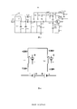
- FIG. 1 is a circuit diagram of a voltage controlled oscillator in the prior art
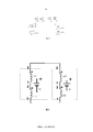
- FIG. 2 is a test diagram of phase noise of the voltage controlled oscillator of FIG. 1 without interference and interference;
- Figure 3 is a circuit diagram of an embodiment of a voltage controlled oscillator of the present invention.
- FIG. 4 is a circuit diagram of an embodiment of the inductor assembly 10 of FIG. 3;
- Figure 5 is a test diagram of the phase noise of the voltage controlled oscillator of Figure 3 in the absence of interference and interference;
- Embodiment 6 is a circuit diagram of Embodiment 2 of an inductance component of a voltage controlled oscillator of the present invention
- Embodiment 7 is a circuit diagram of Embodiment 3 of an inductance component of a voltage controlled oscillator of the present invention.
- Figure 8 is a circuit diagram of a fourth embodiment of an inductive component of a voltage controlled oscillator of the present invention.
- the frequency source includes a phase detector connected in sequence, a charge pump, a loop filter, a voltage controlled oscillator, and a branch connected to the output end of the voltage controlled oscillator and the input end of the phase detector respectively.
- Frequency Regarding the voltage controlled oscillator, in conjunction with the circuit diagram of the first embodiment of the voltage controlled oscillator shown in FIG. 3, the transistor Q1005 is an active oscillating unit, which provides energy for the establishment of the voltage controlled oscillator.
- the wound inductor component 10 provides a DC path for the varactor diodes D1006 and D1007, and the inductor L1016 provides a DC path for the varactor diodes D1004 and D1005.
- the varactor diodes D1006, D1007, D1004, and D1005 generate an adjustable variable capacitance under the action of the RF control voltage (RFCV).
- the shunt capacitor formed by the varactor diodes D1006 and D1007 and the varactor diodes D1004 and D1005 form a shunt capacitor.
- the total series capacitance is formed, and the total series capacitance forms a total parallel capacitance with the capacitor C1099.
- the total parallel capacitance and the inductor L1018 form a parallel resonant unit of inductance and capacitance.
- the resonant frequency of the resonant unit determines the oscillation frequency of the voltage controlled oscillator.
- the resistors R1038, R1039, and R1044 divide the voltage of 5V, and the voltage of the resistor R1044 is supplied with a bias voltage through the inductor (high-frequency choke coil) L1009 to the base of the transistor Q1005.
- the inductors L1015 and L1014 are the collectors of the transistor Q1005, respectively.
- the inductor component includes two winding inductors L1, L2 disposed in parallel and close to each other, wherein the same-name terminal (pin 2) of the winding inductor L1 is The same name end of the winding inductor L2 is connected.
- the different name end of the inductor L1 (pin 1) and the different name end of the inductor L2 (pin 1) serve as a signal input end and an output end, respectively.
- the winding inductances L1 and L2 are preferably the same type of winding inductance of the same manufacturer to ensure that the parameters are consistent.
- the winding inductances L1 and L2 are respectively connected by the same name, thereby ensuring the winding directions of the winding inductances L1 and L2.
- the current is reversed, but the currents of the windings L1 and L2 are parallel and close to each other, which ensures that the electromotive forces induced by the inductors L1 and L2 are equal in magnitude and opposite in polarity, and can cancel each other out.
- the curve S21 is the phase noise data when there is no interference signal
- the curve S22 is the phase noise data after the external interference.
- the phase noise is only deteriorated by 5 dB after being interfered.
- the anti-interference suppression capability is enhanced by 20 dB.
- inductive devices of the voltage controlled oscillator shown in FIG. 3 such as the inductors L1009, L1016, and L1018, may also be replaced by the inductor components in the above embodiments.
- FIG. 6 is a circuit diagram of a second embodiment of an inductor component of a voltage controlled oscillator of the present invention.
- the inductor component of the embodiment includes six winding inductances L1, L2, L3, L4, L5, and L6, wherein the winding inductance L1 and the winding
- the line inductance L2 is parallel and close to the arrangement
- the winding inductance L3 is parallel and close to the winding inductance L4
- the winding inductance L5 is parallel and close to the winding inductance L6.
- the same name end of the winding inductance L1 is connected with the same name end of the winding inductance L2, and the same name end of the winding inductance L3 is connected with the same name end of the winding inductance L4, and the same name end of the winding inductance L5 and the same name of the winding inductance L6 Connected to the end, the different name end of the winding inductance L3 is connected with the different name end of the winding inductance L2, and the different name end of the winding inductance L5 is connected with the different name end of the winding inductance L4, and the different name end of the winding inductance L1 is
- the different names of the winding inductor L6 serve as a signal input terminal and an output terminal, respectively.
- the inductor component of the embodiment includes eight winding inductances L1, L2, L3, L4, L5, L6, L7, L8, wherein the winding The inductor L1 is parallel and close to the winding inductance L2, and the winding inductance L3 is parallel and close to the winding inductance L4.
- the winding inductance L5 is parallel and close to the winding inductance L6, and the winding inductance L7 is parallel to the winding inductance L8. And close to the setting.
- the different name end of the winding inductance L1 is connected with the different name end of the winding inductance L2
- the different name end of the winding inductance L3 is connected with the different name end of the winding inductance L4
- the different name end and winding of the winding inductance L5 The different ends of the line inductance L6 are connected, and the different name end of the winding inductance L7 is connected to the different name end of the winding inductance L8.
- the same name end of the winding inductance L3 is connected with the same name end of the winding inductance L2, and the same name end of the winding inductance L5 is connected with the same name end of the winding inductance L4, and the same name end of the winding inductance L7 is connected with the same name end of the winding inductance L6.
- the same-name end of the winding inductance L1 and the same-name end of the winding inductance L6 serve as a signal input end and an output end, respectively.
- the magnitudes of the electromotive forces induced by the winding inductors L1 and L2 are equal and opposite in polarity.
- the electric potentials induced by the winding inductances L3 and L4 are equal and opposite in polarity, and can cancel each other out;
- the electromotive force induced by the winding inductances L5 and L6 is equal and opposite in polarity, and can cancel each other out.
- the winding electromagnets induced by the winding inductors L7 and L8 have the same magnitude and opposite polarity and can cancel each other out. Therefore, it suppresses external disturbances.
- FIG. 8 is a circuit diagram of a fourth embodiment of an inductor component of the voltage controlled oscillator of the present invention.
- the inductor component of the embodiment is different from the inductor component shown in FIG. 4 only by using two winding inductors L11 connected in series.
- the winding inductance group consisting of L12 is used instead of the winding inductance L1
- the winding inductance group consisting of two series winding inductors L21 and L22 is used instead of the winding inductance L2, and, in these two windings
- the same-named ends of the winding inductors in the same position are respectively close to each other.
- the same-name end of the winding inductance L11 is connected to the same-name end of the winding inductance L21, and the different-name end of the winding inductance L11 Connected to the same-name end of the winding inductance L12, correspondingly, the different-name end of the winding inductance L21 is connected to the same-name end of the winding inductance L22.
- the different end of the winding inductance L12 and the different end of the winding inductance L22 serve as a signal input end and an output end, respectively.
- each winding inductance group includes only two winding inductances connected in series. In actual use, each winding inductance group may also select another number of series windings. The line inductance, as long as the two winding inductors are in the same position, the same name of the winding inductance can be correspondingly close.
- each winding inductance in the inductor assembly shown in FIG. 6 and FIG. 7 can adopt a winding inductance group composed of at least two winding inductors connected in series.
- the number of winding inductance groups in the inductor component is not limited to 2, 6, and 8. In other embodiments, it may be any even array, for example, represented as a 2N group of winding inductance groups, and N is a natural number.
- the odd-numbered array winding inductance group is parallel and close to the winding inductance group adjacent thereto, and the same-name end of the odd-numbered array winding inductance group is connected to the same-name end of the adjacent winding inductance group, the first group
- the different name end of the wound inductor group is a signal input end
- the different name end of the 2N group winding inductance group is a signal output end
- the different name end is connected to the different name end of the winding inductance group adjacent to the front side; or, the different name end of the odd array winding inductance group is connected with the different name end of the adjacent winding inductance group, the first group winding
- the same name end of the line inductance group is the signal input end
- the same name end of the 2N group winding inductance group is the signal output end
- the odd-numbered array winding inductance group is disposed in parallel with the winding inductance group adjacent thereto, and may be arranged in parallel in the horizontal plane or in parallel in the vertical plane, for example, when the odd-numbered array winding inductance group When the winding inductance group adjacent to the rear side is disposed on the same side of the PCB board, the odd-numbered array winding inductance group is disposed in parallel with the winding inductance group adjacent thereto in the horizontal plane; when the PCB board is a double-sided PCB board And the odd-numbered array wound-wound inductor group and the adjacent wound-wound inductor group are respectively disposed at the same positions on both sides of the PCB board, thereby ensuring the odd-numbered array wound-wound inductor group and the winding-wound inductor group adjacent thereto Set in parallel in the vertical plane.
- the voltage controlled oscillator can be placed in the metal shield case.
- the above is a voltage controlled oscillator as an example to illustrate the structure of the inductor component. It should be understood that the structure of the inductor component in the above embodiment can be applied to any voltage sensitive circuit, for example, control. Circuit.
Landscapes
- Engineering & Computer Science (AREA)
- Power Engineering (AREA)
- Inductance-Capacitance Distribution Constants And Capacitance-Resistance Oscillators (AREA)
Abstract
一种电压敏感电路、频率源及其压控振荡器。该压控振荡器包括电感组件,电感组件包括2N组绕线电感组,第奇数组绕线电感组与其后面相邻的绕线电感组平行且靠近设置,当N=1时,第一组绕线电感组的同名端与第二组绕线电感组的同名端相连,第一组绕线电感组的异名端为信号输入端,第二组绕线电感组的异名端为信号输出端;或者,第一组绕线电感组的异名端与第二组绕线电感组的异名端相连,第一组绕线电感组的同名端为信号输入端,第二组绕线电感组的同名端为信号输出端。
Description
本发明涉及无线通信领域,尤其涉及一种电压敏感电路、频率源及其压控振荡器 。
电压敏感电路是指这类电路对不同电压的输入信号呈现出不同的特性,其包括有电感组件。而频率源作为一种电压敏感电路,相位噪声是其重要衡量因素。
在频率源的锁相环中,充电泵所输出的泵电流经过环路滤波器后,形成射频控制电压,以控制压控振荡器的频率。例如,如图1所示的压控振荡器,三极管Q1005是有源振荡单元,为压控振荡器的建立提供能源。绕线电感L5为变容二极管D1006、D1007提供直流通路,电感L1016为D1004、D1005提供直流通路。变容二极管D1006、D1007、D1004、D1005在射频控制电压(RFCV)的作用下,产生可调的变化电容,这些变化电容与后面的电容、电感一并形成谐振单元,该谐振单元的谐振频率决定压控振荡器的振荡频率。
但是,由于压控振荡器的压控增益较高,射频控制电压(RFCV)的微小波动都会转换成相位噪声干扰,导致压控振荡器被干扰,如图2所示,曲线S11为没有干扰信号时的噪声数据,曲线S12为受到外界干扰后的相位噪声数据,从曲线S11、S12可看出,在10KHz频点处,相位噪声受干扰后恶化了25dB。
目前,通常采用以下两种方式来提高频率源的抗干扰能力:
1.
采用电阻替代绕线电感L5,这种方式相比能感应出干扰电压的绕线电感,可减少空间干扰的耦合,提高干扰的抑制能力,但是,这种方式严重增加了噪声电阻。
2.
采用叠层电感替代绕线电感L5,这种方式也能够减小空间干扰的耦合量,但同样会恶化等效噪声电阻(叠层电感的等效串联电阻要大于绕线电感的等效串联电阻)。
综上,以上两种方式都存在减少空间干扰耦合与噪声电阻恶化的矛盾。
本发明要解决的技术问题在于,针对现有技术的上述减少空间干扰耦合与噪声电阻恶化的矛盾的缺陷,提供一种电压敏感电路、频率源及其压控振荡器,能解决减少空间干扰耦合与噪声电阻恶化的矛盾。
本发明解决其技术问题所采用的技术方案是:构造一种电压敏感电路,包括电感组件,所述电感组件包括2N组绕线电感组,N为自然数,第奇数组绕线电感组与其后面相邻的绕线电感组平行且靠近设置;
当N=1时,第一组绕线电感组的同名端与第二组绕线电感组的同名端相连,第一组绕线电感组的异名端为信号输入端,第二组绕线电感组的异名端为信号输出端;或者,第一组绕线电感组的异名端与第二组绕线电感组的异名端相连,第一组绕线电感组的同名端为信号输入端,第二组绕线电感组的同名端为信号输出端;
当N>1时,第奇数组绕线电感组的同名端与其后面相邻的绕线电感组的同名端相连,第一组绕线电感组的异名端为信号输入端,第2N组绕线电感组的异名端为信号输出端,而且,除第一组绕线电感组外的其它第奇数组绕线电感组的异名端分别与其前面相邻的绕线电感组的异名端相连;或者,第奇数组绕线电感组的异名端与其后面相邻的绕线电感组的异名端相连,第一组绕线电感组的同名端为信号输入端,第2N组绕线电感组的同名端为信号输出端,而且,除第一组绕线电感组外的其它第奇数组绕线电感组的同名端分别与其前面相邻的绕线电感组的同名端相连。
在本发明所述的电压敏感电路中,第奇数组绕线电感组与其后面相邻的绕线电感组均包括一个绕线电感。
在本发明所述的电压敏感电路中,第奇数组绕线电感组与其后面相邻的绕线电感组均包括至少两个相串联的绕线电感,且第奇数组绕线电感组与其后面相邻的绕线电感组中相同位置的绕线电感的同名端分别对应靠近。
在本发明所述的电压敏感电路中,第奇数组绕线电感组与其后面相邻的绕线电感组在水平面内平行设置或在垂直面内平行设置。
在本发明所述的电压敏感电路中,所述电压敏感电路设置于金属屏蔽壳内。
本发明还构造一种压控振荡器,包括电感组件,所述电感组件包括2N组绕线电感组,N为自然数,
第奇数组绕线电感组与其后面相邻的绕线电感组平行且靠近设置;
当N=1时,第一组绕线电感组的同名端与其后面相邻的绕线电感组的同名端相连,第一组绕线电感组的异名端为信号输入端,第二组绕线电感组的异名端为信号输出端;或者,第一组绕线电感组的异名端与其后面相邻的绕线电感组的异名端相连,第一组绕线电感组的同名端为信号输入端,第二组绕线电感组的同名端为信号输出端;
当N>1时,第奇数组绕线电感组的同名端与其后面相邻的绕线电感组的同名端相连,第一组绕线电感组的异名端为信号输入端,第2N组绕线电感组的异名端为信号输出端,而且,除第一组绕线电感组外的其它第奇数组绕线电感组的异名端分别与其前面相邻的绕线电感组的异名端相连;或者,第奇数组绕线电感组的异名端与其后面相邻的绕线电感组的异名端相连,第一组绕线电感组的同名端为信号输入端,第2N组绕线电感组的同名端为信号输出端,而且,除第一组绕线电感组外的其它第奇数组绕线电感组的同名端分别与其前面相邻的绕线电感组的同名端相连。
在本发明所述的压控振荡器中,第奇数组绕线电感组与其后面相邻的绕线电感组均包括一个绕线电感;或者,
第奇数组绕线电感组与其后面相邻的绕线电感组均包括至少两个相串联的绕线电感,且第奇数组绕线电感组与其后面相邻的绕线电感组中相同位置的绕线电感的同名端分别对应靠近。
在本发明所述的压控振荡器中,第奇数组绕线电感组与其后面相邻的绕线电感组在水平面内平行设置或在垂直面内平行设置。
在本发明所述的压控振荡器中,所述压控振荡器设置于金属屏蔽壳内。
本发明还构造一种频率源,包括以上所述的压控振荡器。
下面将结合附图及实施例对本发明作进一步说明,附图中:
图1是现有技术中的一种压控振荡器的电路图;
图2是图1中的压控振荡器在没有受到干扰和受到干扰时的相位噪声的测试图;
图3是本发明 压控振荡器实施例的电路图;
图4是图3中电感组件10实施例一电路图;
图5是图3中的压控振荡器在没有受到干扰和受到干扰时的相位噪声的测试图;
图6是本发明压控振荡器的电感组件实施例二的电路图;
图7是本发明压控振荡器的电感组件实施例三的电路图;
图8是本发明压控振荡器的电感组件实施例四的电路图。
首先说明的是,频率源包括有依次连接的鉴相器、充电泵、环路滤波器、压控振荡器,还包括分别与压控振荡器的输出端和鉴相器的输入端相连的分频器。关于压控振荡器,结合图3所示的压控振荡器实施例一的电路图,三极管Q1005是有源振荡单元,为压控振荡器的建立提供能源。绕线电感组件10为变容二极管D1006、D1007提供直流通路,电感L1016为变容二极管D1004、D1005提供直流通路。变容二极管D1006、D1007、D1004、D1005在射频控制电压(RFCV)的作用下,产生可调的变化电容,由变容二极管D1006、D1007形成的并联电容与变容二极管D1004、D1005形成的并联电容串联后,再与电容C1075串联,构成的总的串联电容,该总的串联电容再与电容C1099形成一个总的并联电容,该总的并联电容与电感L1018形成电感、电容的并联谐振单元,该谐振单元的谐振频率决定压控振荡器的振荡频率。电阻R1038、R1039、R1044对5V电压进行分压,电阻R1044的电压经过电感(高频扼流线圈)L1009给三极管Q1005的基极提供偏置电压,电感L1015、L1014分别为三极管Q1005的集电极、发射极的高频扼流线圈,电容C1088提供正反馈信号,电容C1078为谐振单元的接入电容。
在该压控振荡器中,关于电感组件10,结合图4,该电感组件包括平行且靠近设置的两个绕线电感L1、L2,其中,绕线电感L1的同名端(引脚2)与绕线电感L2的同名端相连。电感L1的异名端(引脚1)和电感L2的异名端(引脚1)分别作为信号输入端和输出端。另外,绕线电感L1、L2优选同一厂家同一型号的绕线电感,以保证其参数一致。
在该压控振荡器工作时,若射频控制电压(RFCV)因受外界干扰而引起微小波动,绕线电感L1、L2由于其同名端分别相连,保证了绕线电感L1、L2的绕线方向一致,但通过的电流相反,而且,绕线电感L1、L2由于平行且靠近设置,保证了电感L1、L2分别所感应出的电动势幅度相等且极性相反,可以相互抵消。结合图5,曲线S21为没有干扰信号时的相位噪声数据,曲线S22为受到外界干扰后的相位噪声数据,从曲线S21、S22可看出,相位噪声受干扰后仅恶化了5dB。相比图2,抗干扰抑制能力增强了20dB。
在此需说明的是,图3所示的压控振荡器的其它电感器件,如,电感L1009、L1016、L1018也可用上述实施例中的电感组件来替代。
图6是本发明压控振荡器的电感组件实施例二的电路图,该实施例的电感组件包括六个绕线电感L1、L2、L3、L4、L5、L6,其中,绕线电感L1与绕线电感L2平行且靠近设置,绕线电感L3与绕线电感L4平行且靠近设置,绕线电感L5与绕线电感L6平行且靠近设置。而且,绕线电感L1的同名端与绕线电感L2的同名端相连,绕线电感L3的同名端与绕线电感L4的同名端相连,绕线电感L5的同名端与绕线电感L6的同名端相连,绕线电感L3的异名端与绕线电感L2的异名端相连,绕线电感L5的异名端与绕线电感L4的异名端相连,绕线电感L1的异名端与绕线电感L6的异名端分别作为信号输入端和输出端。
同样地,在该电感组件所在的压控振荡器工作时,若射频控制电压(RFCV)因受外界干扰而引起微小波动,绕线电感L1、L2分别所感应出的电动势幅度相等且极性相反,可以相互抵消;绕线电感L3、L4分别所感应出的电动势幅度相等且极性相反,可以相互抵消;绕线电感L5、L6分别所感应出的电动势幅度相等且极性相反,可以相互抵消。因此,对外界干扰起到了抑制效果。
图7是本发明压控振荡器的电感组件实施例三的电路图,该实施例的电感组件包括八个绕线电感L1、L2、L3、L4、L5、L6、L7、L8,其中,绕线电感L1与绕线电感L2平行且靠近设置,绕线电感L3与绕线电感L4平行且靠近设置,绕线电感L5与绕线电感L6平行且靠近设置,绕线电感L7与绕线电感L8平行且靠近设置。而且,绕线电感L1的异名端与绕线电感L2的异名端相连,绕线电感L3的异名端与绕线电感L4的异名端相连,绕线电感L5的异名端与绕线电感L6的异名端相连,绕线电感L7的异名端与绕线电感L8的异名端相连。绕线电感L3的同名端与绕线电感L2的同名端相连,绕线电感L5的同名端与绕线电感L4的同名端相连,绕线电感L7的同名端与绕线电感L6的同名端相连,绕线电感L1的同名端与绕线电感L6的同名端分别作为信号输入端和输出端。
同样地,在该电感组件所在的压控振荡器工作时,若射频控制电压(RFCV)因受外界干扰而引起微小波动,绕线电感L1、L2分别所感应出的电动势幅度相等且极性相反,可以相互抵消;绕线电感L3、L4分别所感应出的电动势幅度相等且极性相反,可以相互抵消;绕线电感L5、L6分别所感应出的电动势幅度相等且极性相反,可以相互抵消;绕线电感L7、L8分别所感应出的电动势幅度相等且极性相反,可以相互抵消。因此,对外界干扰起到了抑制效果。
图8是本发明压控振荡器的电感组件实施例四的电路图,该实施例的电感组件相比图4所示的电感组件,所不同的仅是,采用由两个串联的绕线电感L11、L12所组成的绕线电感组来替代绕线电感L1,采用由两个串联的绕线电感L21、L22所组成的绕线电感组来替代绕线电感L2,而且,在这两个绕线电感组中,相同位置的绕线电感的同名端分别对应靠近,例如,在该实施例中,绕线电感L11的同名端与绕线电感L21的同名端相连,绕线电感L11的异名端与绕线电感L12的同名端相连,相应地,绕线电感L21的异名端与绕线电感L22的同名端相连。绕线电感L12的异名端及绕线电感L22的异名端分别作为信号输入端和输出端。当然,在其它实施例中,也可将绕线电感L12的异名端与绕线电感L11的异名端相连,相应地,将绕线电感L22的异名端与绕线电感L21的异名端相连,绕线电感L12的同名端及绕线电感L22的同名端分别作为信号输入端和输出端。另外,需说明的是,在该实施例中,每个绕线电感组仅包括两个串联的绕线电感,在实际使用时,每个绕线电感组还可选择其它数量个相串联的绕线电感,只要保证这两个绕线电感组中,相同位置的绕线电感的同名端分别对应靠近即可。
基于图8所示的实施例,相应地,图6、图7所示的电感组件中的每个绕线电感,均可采用由至少两个相串联的绕线电感所组成的绕线电感组来替代。另外,电感组件中的绕线电感组的数量也不限于2、6、8,在其它实施例中,可以为任意偶数组,例如,表示为2N组绕线电感组,N为自然数。第奇数组绕线电感组与其后面相邻的绕线电感组平行且靠近设置,而且,第奇数组绕线电感组的同名端与其后面相邻的绕线电感组的同名端相连,第一组绕线电感组的异名端为信号输入端,第2N组绕线电感组的异名端为信号输出端,而且,除第一组绕线电感组外的其它第奇数组绕线电感组的异名端与其前面相邻的绕线电感组的异名端相连;或者,第奇数组绕线电感组的异名端与其后面相邻的绕线电感组的异名端相连,第一组绕线电感组的同名端为信号输入端,第2N组绕线电感组的同名端为信号输出端,而且,除第一组绕线电感组外的其它第奇数组绕线电感组的同名端分别与其前面相邻的绕线电感组的同名端相连。
另外,关于第奇数组绕线电感组与其后面相邻的绕线电感组平行设置,可以是在水平面内平行设置,也可以是在垂直面内平行设置,例如,当第奇数组绕线电感组与其后面相邻的绕线电感组均设置在PCB板的同一面时,将第奇数组绕线电感组与其后面相邻的绕线电感组在水平面内平行设置;当PCB板为双面PCB板,且第奇数组绕线电感组与其后面相邻的绕线电感组分别设置在PCB板的两个面的相同位置时,可保证第奇数组绕线电感组与其后面相邻的绕线电感组在垂直面内平行设置。
优选地,为进一步地抑制干扰,可将压控振荡器设置于金属屏蔽壳内。
最后需说明的是,以上都是以压控振荡器为例来说明电感组件的结构的,应理解,上述实施例中的电感组件的结构可应用于任何对电压敏感的电路中,例如,控制电路。
以上所述仅为本发明的优选实施例而已,并不用于限制本发明,对于本领域的技术人员来说,本发明可以有各种更改和变化。凡在本发明的精神和原则之内,所作的任何修改、等同替换、改进等,均应包含在本发明的权利要求范围之内。
Claims (10)
- 一种电压敏感电路,包括电感组件,其特征在于,所述电感组件包括2N组绕线电感组,N为自然数,第奇数组绕线电感组与其后面相邻的绕线电感组平行且靠近设置;当N=1时,第一组绕线电感组的同名端与第二组绕线电感组的同名端相连,第一组绕线电感组的异名端为信号输入端,第二组绕线电感组的异名端为信号输出端;或者,第一组绕线电感组的异名端与第二组绕线电感组的异名端相连,第一组绕线电感组的同名端为信号输入端,第二组绕线电感组的同名端为信号输出端;当N>1时,第奇数组绕线电感组的同名端与其后面相邻的绕线电感组的同名端相连,第一组绕线电感组的异名端为信号输入端,第2N组绕线电感组的异名端为信号输出端,而且,除第一组绕线电感组外的其它第奇数组绕线电感组的异名端分别与其前面相邻的绕线电感组的异名端相连;或者,第奇数组绕线电感组的异名端与其后面相邻的绕线电感组的异名端相连,第一组绕线电感组的同名端为信号输入端,第2N组绕线电感组的同名端为信号输出端,而且,除第一组绕线电感组外的其它第奇数组绕线电感组的同名端分别与其前面相邻的绕线电感组的同名端相连。
- 根据权利要求1所述的电压敏感电路,其特征在于,第奇数组绕线电感组与其后面相邻的绕线电感组均包括一个绕线电感。
- 根据权利要求1所述的电压敏感电路,其特征在于,第奇数组绕线电感组与其后面相邻的绕线电感组均包括至少两个相串联的绕线电感,且第奇数组绕线电感组与其后面相邻的绕线电感组中相同位置的绕线电感的同名端分别对应靠近。
- 根据权利要求1所述的电压敏感电路,其特征在于,第奇数组绕线电感组与其后面相邻的绕线电感组在水平面内平行设置或在垂直面内平行设置。
- 根据权利要求1所述的电压敏感电路,其特征在于,所述电压敏感电路设置于金属屏蔽壳内。
- 一种压控振荡器,包括电感组件,其特征在于,所述电感组件包括2N组绕线电感组,N为自然数,第奇数组绕线电感组与其后面相邻的绕线电感组平行且靠近设置;当N=1时,第一组绕线电感组的同名端与第二组绕线电感组的同名端相连,第一组绕线电感组的异名端为信号输入端,第二组绕线电感组的异名端为信号输出端;或者,第一组绕线电感组的异名端与第二组绕线电感组的异名端相连,第一组绕线电感组的同名端为信号输入端,第二组绕线电感组的同名端为信号输出端;当N>1时,第奇数组绕线电感组的同名端与其后面相邻的绕线电感组的同名端相连,第一组绕线电感组的异名端为信号输入端,第2N组绕线电感组的异名端为信号输出端,而且,除第一组绕线电感组外的其它第奇数组绕线电感组的异名端分别与其前面相邻的绕线电感组的异名端相连;或者,第奇数组绕线电感组的异名端与其后面相邻的绕线电感组的异名端相连,第一组绕线电感组的同名端为信号输入端,第2N组绕线电感组的同名端为信号输出端,而且,除第一组绕线电感组外的其它第奇数组绕线电感组的同名端分别与其前面相邻的绕线电感组的同名端相连 。
- 根据权利要求6所述的压控振荡器,其特征在于,第奇数组绕线电感组与其后面相邻的绕线电感组均包括一个绕线电感;或者,第奇数组绕线电感组与其后面相邻的绕线电感组均包括至少两个相串联的绕线电感,且第奇数组绕线电感组与其后面相邻的绕线电感组中相同位置的绕线电感的同名端分别对应靠近。
- 根据权利要求6所述的压控振荡器,其特征在于,第奇数组绕线电感组与其后面相邻的绕线电感组在水平面内平行设置或在垂直面内平行设置。
- 根据权利要求6所述的压控振荡器,其特征在于,所述压控振荡器设置于金属屏蔽壳内。
- 一种频率源,其特征在于,包括权利要求6-9任一项所述的压控振荡器。
Priority Applications (1)
| Application Number | Priority Date | Filing Date | Title |
|---|---|---|---|
| PCT/CN2013/089072 WO2015085512A1 (zh) | 2013-12-11 | 2013-12-11 | 一种电压敏感电路、频率源及其压控振荡器 |
Applications Claiming Priority (1)
| Application Number | Priority Date | Filing Date | Title |
|---|---|---|---|
| PCT/CN2013/089072 WO2015085512A1 (zh) | 2013-12-11 | 2013-12-11 | 一种电压敏感电路、频率源及其压控振荡器 |
Publications (1)
| Publication Number | Publication Date |
|---|---|
| WO2015085512A1 true WO2015085512A1 (zh) | 2015-06-18 |
Family
ID=53370475
Family Applications (1)
| Application Number | Title | Priority Date | Filing Date |
|---|---|---|---|
| PCT/CN2013/089072 Ceased WO2015085512A1 (zh) | 2013-12-11 | 2013-12-11 | 一种电压敏感电路、频率源及其压控振荡器 |
Country Status (1)
| Country | Link |
|---|---|
| WO (1) | WO2015085512A1 (zh) |
Citations (5)
| Publication number | Priority date | Publication date | Assignee | Title |
|---|---|---|---|---|
| JP2002009544A (ja) * | 2000-06-19 | 2002-01-11 | Nec Corp | 電圧制御発振器 |
| TW200919945A (en) * | 2007-10-26 | 2009-05-01 | Realtek Semiconductor Corp | Voltage controlled oscillator |
| CN101567662A (zh) * | 2008-04-22 | 2009-10-28 | 联发科技股份有限公司 | 压控振荡器 |
| CN202333790U (zh) * | 2011-12-05 | 2012-07-11 | 黄兴英 | 一种抑制干扰信号和浪涌防护的电路 |
| US20130300476A1 (en) * | 2012-05-08 | 2013-11-14 | Tagarray, Inc. | Low noise and low power voltage controlled oscillators |
-
2013
- 2013-12-11 WO PCT/CN2013/089072 patent/WO2015085512A1/zh not_active Ceased
Patent Citations (5)
| Publication number | Priority date | Publication date | Assignee | Title |
|---|---|---|---|---|
| JP2002009544A (ja) * | 2000-06-19 | 2002-01-11 | Nec Corp | 電圧制御発振器 |
| TW200919945A (en) * | 2007-10-26 | 2009-05-01 | Realtek Semiconductor Corp | Voltage controlled oscillator |
| CN101567662A (zh) * | 2008-04-22 | 2009-10-28 | 联发科技股份有限公司 | 压控振荡器 |
| CN202333790U (zh) * | 2011-12-05 | 2012-07-11 | 黄兴英 | 一种抑制干扰信号和浪涌防护的电路 |
| US20130300476A1 (en) * | 2012-05-08 | 2013-11-14 | Tagarray, Inc. | Low noise and low power voltage controlled oscillators |
Similar Documents
| Publication | Publication Date | Title |
|---|---|---|
| JP6607922B2 (ja) | モバイル装置用途向け無線エネルギ伝送 | |
| US10003316B2 (en) | Device and method for filtering electromagnetic interference | |
| JPH01220415A (ja) | Acラインフィルタ | |
| KR102162654B1 (ko) | 자기 공진 인덕터를 이용한 소형 고전압 알에프 발생기 | |
| CN104769686B (zh) | Rf变压器 | |
| JPS59141801A (ja) | 携帯無線装置用のダイポ−ルアンテナ | |
| US6512422B2 (en) | Oscillator with improved magnetic coupling rejection | |
| CN108199494B (zh) | 一种增益可调的有源负载无线充电装置及其调节方法 | |
| CN110340746B (zh) | 一种用于超声加工系统声学性能开发调试的动态匹配箱 | |
| CN203101479U (zh) | 一种电流检测电路 | |
| JP6315109B2 (ja) | 給電装置 | |
| WO2015085512A1 (zh) | 一种电压敏感电路、频率源及其压控振荡器 | |
| CN110571127B (zh) | 用于多极杆离子阱和离子导向装置的射频电源 | |
| Detti et al. | A compact radiofrequency drive based on interdependent resonant circuits for precise control of ion traps | |
| KR20180131608A (ko) | 차폐된 케이블을 통해 공진기 커패시터에 커플링되는 센서 인덕터를 가지는 센서 공진기를 사용하는 원격 감지 | |
| US12573550B2 (en) | Switch current sensors | |
| JP2012175880A (ja) | 非接触給電装置 | |
| Halivni et al. | Current controlled transmitter for high frequency WPT utilizing non-invasive PCB integrated rogowski current sensor | |
| CN110289819A (zh) | 一种射频前端及其射频功率放大器的输出匹配网络 | |
| CN210866122U (zh) | 用于多极杆离子阱和离子导向装置的射频电源 | |
| Zhao et al. | Extending the bandwidth of piezo-electric energy harvesting through the use of bias flip | |
| CN203608180U (zh) | 一种电压敏感电路、频率源及其压控振荡器 | |
| JP6690422B2 (ja) | Esr検出器 | |
| SU849392A1 (ru) | Индуктивно-емкостной преобразователь | |
| WO2003100972A1 (en) | Complex resonance circuit and filter |
Legal Events
| Date | Code | Title | Description |
|---|---|---|---|
| 121 | Ep: the epo has been informed by wipo that ep was designated in this application |
Ref document number: 13899211 Country of ref document: EP Kind code of ref document: A1 |
|
| NENP | Non-entry into the national phase |
Ref country code: DE |
|
| 122 | Ep: pct application non-entry in european phase |
Ref document number: 13899211 Country of ref document: EP Kind code of ref document: A1 |