WO2015083749A1 - センサチップ及びバイオセンサシステム - Google Patents
センサチップ及びバイオセンサシステム Download PDFInfo
- Publication number
- WO2015083749A1 WO2015083749A1 PCT/JP2014/082029 JP2014082029W WO2015083749A1 WO 2015083749 A1 WO2015083749 A1 WO 2015083749A1 JP 2014082029 W JP2014082029 W JP 2014082029W WO 2015083749 A1 WO2015083749 A1 WO 2015083749A1
- Authority
- WO
- WIPO (PCT)
- Prior art keywords
- electrode
- substance
- electrode group
- capturing
- electrodes
- Prior art date
- Legal status (The legal status is an assumption and is not a legal conclusion. Google has not performed a legal analysis and makes no representation as to the accuracy of the status listed.)
- Ceased
Links
Images














Classifications
-
- G—PHYSICS
- G01—MEASURING; TESTING
- G01N—INVESTIGATING OR ANALYSING MATERIALS BY DETERMINING THEIR CHEMICAL OR PHYSICAL PROPERTIES
- G01N27/00—Investigating or analysing materials by the use of electric, electrochemical, or magnetic means
- G01N27/02—Investigating or analysing materials by the use of electric, electrochemical, or magnetic means by investigating impedance
- G01N27/22—Investigating or analysing materials by the use of electric, electrochemical, or magnetic means by investigating impedance by investigating capacitance
- G01N27/221—Investigating or analysing materials by the use of electric, electrochemical, or magnetic means by investigating impedance by investigating capacitance by investigating the dielectric properties
-
- G—PHYSICS
- G01—MEASURING; TESTING
- G01N—INVESTIGATING OR ANALYSING MATERIALS BY DETERMINING THEIR CHEMICAL OR PHYSICAL PROPERTIES
- G01N33/00—Investigating or analysing materials by specific methods not covered by groups G01N1/00 - G01N31/00
- G01N33/48—Biological material, e.g. blood, urine; Haemocytometers
- G01N33/50—Chemical analysis of biological material, e.g. blood, urine; Testing involving biospecific ligand binding methods; Immunological testing
- G01N33/53—Immunoassay; Biospecific binding assay; Materials therefor
- G01N33/543—Immunoassay; Biospecific binding assay; Materials therefor with an insoluble carrier for immobilising immunochemicals
- G01N33/54366—Apparatus specially adapted for solid-phase testing
- G01N33/54373—Apparatus specially adapted for solid-phase testing involving physiochemical end-point determination, e.g. wave-guides, FETS, gratings
- G01N33/5438—Electrodes
Definitions
- the present disclosure relates to a technique for electrically detecting a biological substance in a specimen.
- JP 2010-160151 A discloses that an antibody layer having specific binding reactivity with an antigen is immobilized on at least one surface of two electrodes. The change in the conductive property between the two electrodes due to the capture of the antigen by the antibody serves as an index for the electrical sensing of the antigen.
- the present application discloses a biosensor that enables highly accurate detection of a biological substance.
- the sensor chip disclosed in the present application is provided with an insulating film having a capturing surface on which a capturing substance that reacts or binds to a biological substance to be measured is fixed, and is provided on the opposite side of the capturing surface of the insulating film. And a plurality of electrodes provided side by side in one direction.
- the supplementary substance is formed on the capture surface in at least one of a region overlapping with the plurality of electrodes or a region sandwiched between at least two of the plurality of electrodes in a plan view.
- a biosensor that enables highly accurate detection of a biological substance can be realized.
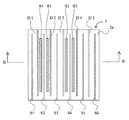
- FIG. 1A is a plan view illustrating a configuration example of a sensor chip of the biosensor according to the embodiment.
- 1B is a cross-sectional view of the sensor chip shown in FIG. 1A taken along line BB.
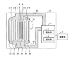
- FIG. 2 is a configuration example of a biosensor system.
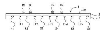
- FIG. 3A is a plan view showing a modified example of the arrangement of the capturing substance R.
- FIG. 3B is a cross-sectional view of the sensor chip 1 shown in FIG. 3A.
- FIG. 4A is a cross-sectional view illustrating an example of a connection form of the sensor chip.
- FIG. 4B is a cross-sectional view illustrating another example of the connection form of the sensor chip.
- FIG. 1A is a plan view illustrating a configuration example of a sensor chip of the biosensor according to the embodiment.
- 1B is a cross-sectional view of the sensor chip shown in FIG. 1A taken along line BB.
- FIG. 2 is a configuration example of a bio
- FIG. 5 is a flowchart showing an operation example of the biosensor in the present embodiment.
- FIG. 6A is a diagram illustrating an example of a part of electric lines of force when driving the sensor chip 1 in a state where a specimen is not dropped and a signal output from the first electrode.
- FIG. 6B is a diagram illustrating an example of a part of electric lines of force when the sensor chip 1 is driven after the sample is dropped and a signal output from the first electrode.
- FIG. 7 is a flowchart showing another operation example of the biosensor.
- FIG. 8 is a diagram showing an example of a part of the electric lines of force when the sensor chip 1 is driven after the sample is dropped and signals output from the first electrodes S1 to S6.
- FIG. 6A is a diagram illustrating an example of a part of electric lines of force when driving the sensor chip 1 in a state where a specimen is not dropped and a signal output from the first electrode.
- FIG. 6B is a diagram illustrating an example of a part of
- FIG. 10A is a diagram illustrating an example of mutual capacitance values measured in advance in a predetermined environment for use in calibration.
- FIG. 10B is a diagram illustrating an example of the mutual capacitance value detected by the detection unit 6 after the specimen is supplied to the sensor chip 1.
- FIG. 11A is a diagram illustrating an example of a manufacturing process of a sensor chip.
- FIG. 11B is a diagram for explaining an example of the manufacturing process of the sensor chip.
- FIG. 11C is a diagram for explaining an example of the manufacturing process of the sensor chip.
- FIG. 11D is a diagram for explaining an example of the manufacturing process of the sensor chip.
- FIG. 11E is a diagram for explaining an example of the manufacturing process of the sensor chip.
- FIG. 12 is a diagram illustrating an example of a region where the ligand R is formed.
- FIG. 13A is a diagram illustrating an example of a manufacturing process of a sensor chip.
- FIG. 13B is a diagram illustrating an example of the manufacturing process of the sensor chip.
- FIG. 14A is a diagram illustrating an example of a manufacturing process of a sensor chip.
- FIG. 14B is a diagram for explaining an example of the manufacturing process of the sensor chip.
- FIG. 14C is a diagram for explaining an example of the manufacturing process of the sensor chip.
- FIG. 14D is a diagram for explaining an example of the manufacturing process of the sensor chip.
- FIG. 15 is a diagram for explaining an example of the manufacturing process of the sensor chip.
- FIG. 16 is a plan view showing a modified example of the configuration of the sensor chip.
- FIG. 17 is a cross-sectional view taken along line L of the sensor chip shown in FIG.
- FIG. 18 is an enlarged view near the intersection of the first electrode S3 and the second electrode D3 of the sensor chip shown in FIG.
- FIG. 19 shows a modification of the configuration of the portion shown in the enlarged view of FIG.
- FIG. 20 is a plan view showing a modification of the configuration of the sensor chip.
- 21 is a cross-sectional view taken along line L of the sensor chip shown in FIG.
- FIG. 22 shows a modification of the configuration shown in FIG.
- FIG. 23 is a plan view showing a modified example of the configuration of the sensor chip.
- 24 is a sectional view taken along line L of the sensor chip shown in FIG.
- FIG. 25 is a cross-sectional view showing a modified example of the configuration of the sensor chip.
- a sensor chip includes an insulating film having a capturing surface to which a capturing substance that reacts or binds to a biological substance to be measured is fixed, and the insulating film on the side opposite to the capturing surface.
- a plurality of electrodes provided side by side in at least one direction.
- the supplementary substance is formed on the capture surface in at least one of a region overlapping with the plurality of electrodes or a region sandwiched between at least two of the plurality of electrodes in a plan view.
- the capacitance value between the plurality of electrodes provided on the side opposite to the capture surface of the insulating film having the capture surface for capturing the biological substance to be measured is detected.
- the value of the capacitance between the plurality of electrodes reflects the state of the electric field on the trapping surface of the insulating film.
- the capturing substance reacts with or binds to the biological substance to be measured on a part of the capturing surface, the electric field around the biological substance changes. This change in electric field is reflected in the detected capacitance value.
- the capacitance value By detecting the capacitance value, the position and amount of the biological substance on the capturing surface can be detected.
- the influence of the oxidation or contamination of the electrodes on the detection accuracy is reduced.
- the capacitance values formed at a plurality of locations on the capture surface can be detected by a plurality of electrodes provided side by side in at least one direction, it is possible to detect subtle changes in potential on the capture surface. It becomes possible. As a result, it is possible to detect a biological substance with high accuracy.
- the form of the plurality of electrodes provided on the side of the insulating film opposite to the capturing surface is limited to the case where the plurality of electrodes are formed so as to contact the surface of the insulating film opposite to the capturing surface. Absent.
- at least one additional insulating film may be provided between the surface opposite to the capturing surface of the insulating film having the capturing surface and the plurality of electrodes.
- the form of the insulating film having the trapping surface is not limited to the case where the trapping substance is directly fixed on the insulating film.
- a film for fixing the capturing substance may be provided on the insulating film, and the capturing substance may be fixed to the film.
- the plurality of electrodes may include a first electrode group arranged in at least one direction and a second electrode group arranged in the same direction as the one direction.
- at least one second electrode may be arranged between at least one pair of two adjacent first electrodes in the first electrode group.
- the trapping substance can be formed between the first electrode and the second electrode in plan view. As a result, since the capturing substance is disposed in the portion where the capacitance between the first electrode and the second electrode is formed, the biological substance can be detected with high accuracy.
- the plurality of electrodes may include a first electrode group provided side by side in the at least one direction and a second electrode group that intersects the first electrode group in plan view.
- the electrostatic capacitance formed by the first electrode and the second electrode can be arranged in a matrix on the capturing surface. For this reason, the degree of freedom of arrangement of the capturing substance is increased.
- a plurality of capturing substances when disposed, they can be efficiently disposed on the capturing surface.
- the distribution of the biological substance on the capture surface can be detected in more detail.
- the supplementary substance is a region sandwiched between the first electrode and the second electrode around the intersection of the first electrode and the second electrode in a plan view, or the first substance around the intersection. It can be formed at a position overlapping a region including a region sandwiched between one electrode and the second electrode and the intersection. As a result, since the capturing substance is disposed in the portion where the capacitance between the first electrode and the second electrode is formed, the biological substance can be detected with high accuracy.
- the supplementary substance may be formed on the capturing surface at a position overlapping all the plurality of electrodes in plan view. Thereby, the measurement target substance can be captured in a wide range on the capture surface. In addition, the manufacturing process can be simplified.
- the capture surface includes a region where the capture material is fixed and a region where the capture material is not provided.
- the capture surface includes a region where the capture material is fixed and a region where the capture material is not provided.
- a plurality of capture substances that react or bind to different biological substances to be measured may be fixed to different areas on the capture surface. Thereby, a plurality of different types of biological substances can be detected on the capture surface.
- the plurality of electrodes may include a plurality of first electrode groups and a plurality of second electrode groups. At least a part of at least one second electrode of the second electrode group is disposed between two adjacent first electrodes of the first electrode group, and the first electrode group and the second electrode group Is connected to a terminal to which a drive signal is input, and the other of the first electrode group and the second electrode group is a mutual electrostatic voltage generated between the first electrode and the second electrode by the drive signal. It can be configured to be connected to a terminal that outputs a signal corresponding to the capacitance.
- one of the first electrode group and the second electrode group is a drive line to which a drive signal is input, and the other of the first electrode group and the second electrode group is the first electrode by the drive signal.
- a sense line that outputs a signal corresponding to the mutual capacitance generated between the first electrode and the second electrode.
- the biosensor system connected to the sensor chip includes: a drive unit that inputs a drive signal to any one of a first electrode group and a second electrode group included in the plurality of electrodes of the sensor chip; Of the electrode group and the second electrode group, a signal output from an electrode group other than the electrode group to which the drive signal is input is measured, and based on the obtained signal, between the second electrode group and the first electrode group And a detecting unit for detecting the value of the mutual capacitance.
- the detection unit can calculate a difference between signals output between two second electrodes in the second electrode group, and use the difference value to calculate the mutual capacitance value. Thereby, it is possible to obtain a capacitance value with less noise components. As a result, the detection accuracy is further improved. Note that the calculation of the difference can also be executed by an arithmetic unit described later.
- the biosystem generates data indicating the presence / absence or amount of the biological substance to be measured or an image indicating the distribution of the biological substance on the capture surface based on the capacitance value detected by the detection unit.
- the operation unit can be further provided. In this manner, information indicating the presence / absence, amount or distribution of a biological substance can be obtained from the detected capacitance.
- the calculation unit is detected by the detection unit in a state where the sample is provided on the capture surface and a value of a mutual capacitance detected by the detection unit when the sample is not supplied to the capture surface.
- the mutual electrostatic capacitance value can be used to generate data indicating the presence or amount of the biological substance to be measured or an image indicating the distribution of the biological substance on the capture surface. Thereby, the value which shows the change of the electrostatic capacitance resulting from a biological substance can be obtained. Therefore, since the capacitance value with reduced noise is used, the accuracy of detection of the presence / absence, amount or distribution of a biological substance is further improved.
- the calculation unit uses a capacitance value in a region where the capturing substance of the capturing surface is fixed and a capacitance value in a region where the capturing substance of the capturing surface is not provided, Data indicating the presence or absence or amount of the biological substance to be measured or an image indicating the distribution of the biological substance on the capturing surface can be generated. Thereby, the value which shows the change of the electrostatic capacitance resulting from a biological substance can be obtained. Therefore, since the capacitance value with reduced noise is used, the accuracy of detection of the presence / absence, amount or distribution of a biological substance is further improved.
- the calculation unit is configured to measure and record a mutual capacitance value in a region where the capturing substance on the capturing surface is fixed and a mutual electrostatic capacitance in the region where the capturing material is not provided on the capturing surface. Using the capacitance value, the mutual capacitance value detected by the detection unit can be calibrated. Thereby, since the capacitance value in which noise caused by environmental changes or the like is further reduced is used, the accuracy of detection of the presence / absence, amount or distribution of a biological substance is further improved.
- the first electrode group includes a plurality of lines, and the plurality of lines included in the second electrode group are adjacent to any line of the first electrode group, and the first electrode line and the first electrode adjacent thereto
- the distance between the two electrode lines is constant, and the trapping substance is provided between at least one line of the first electrode group and the adjacent second electrode line in plan view. It may be a configuration.
- the 1st electrode group and the 2nd electrode group can be made into the simple composition which arranged a plurality of lines.
- the capturing substance is disposed in the portion where the capacitance between the first electrode and the second electrode is formed, the biological substance can be detected with high accuracy.
- the first electrode group includes a plurality of lines arranged at equal intervals
- the second electrode group includes a plurality of lines intersecting the plurality of lines of the first electrode group in plan view
- the substance may be provided in at least one of a region surrounded by two adjacent lines of the first electrode group and two adjacent lines of the second electrode group in plan view.
- a plurality of electrodes, and the supplementary substance is at least one of a region overlapping with the plurality of electrodes or a region sandwiched between at least two of the plurality of electrodes in the plan view.
- a method of measuring the biological material using the formed sensor chip is also one embodiment of the present invention. The method includes inputting a drive signal to one of the first electrode group and the second electrode group included in the plurality of electrodes of the sensor chip, and out of the first electrode group and the second electrode group.
- a signal output from an electrode group other than the electrode group to which the drive signal is input is measured, and a mutual capacitance value between the second electrode group and the first electrode group is determined based on the obtained signal.
- a step of detecting, and using the detected value of the mutual capacitance a step of generating data indicating the presence or amount of the biological substance to be measured or an image indicating the distribution of the biological substance on the capture surface And having.
- the first electrode group is provided for a biosensor including a plurality of first electrode groups and a plurality of second electrode groups located on the opposite side of the capturing surface of the biological substance to be measured with an insulating film therebetween.
- the mutual capacitance value between the first electrode group and the second electrode group is calculated using the response signal of the second electrode group or the first electrode group with respect to the drive signal input to the second electrode group.
- Information indicating the distribution of the biological substance on the capturing surface is obtained from the value of the mutual capacitance. Therefore, it becomes possible to detect a biological substance with high accuracy.
- the difference between the capacitances detected by the two electrodes of the first electrode group can be calculated as the mutual capacitance value. In this case, it is possible to obtain a capacitance value having a smaller noise component and a larger component due to a change in capacitance due to the biological substance to be measured.
- a plurality of electrodes, and the supplementary substance is at least one of a region overlapping with the plurality of electrodes or a region sandwiched between at least two of the plurality of electrodes in the plan view.
- a program for causing a computer to process data obtained by the sensor chip and measuring the biological material is also an embodiment of the present invention.
- the program is output from an electrode group other than the electrode group to which the drive signal is input according to the drive signal input to either one of the first electrode group and the second electrode group included in the plurality of electrodes.
- a process of acquiring a value of mutual capacitance between the second electrode group and the first electrode group detected based on a signal to be detected, and the living body to be measured using the value of the mutual capacitance And processing for generating data indicating the presence or absence or amount of the derived material or an image indicating the distribution of the biological material on the capturing surface.
- a biosensor includes an insulating film having a capturing surface on which a capturing substance that reacts or binds to a biological substance to be measured is fixed, and the side of the insulating film opposite to the capturing surface
- a plurality of first electrode groups provided side by side in at least one direction and a region between the plurality of first electrode groups in plan view, provided on a side opposite to the capturing surface of the insulating film
- a plurality of second electrode groups provided in the first electrode group, a drive unit for inputting a drive signal to the second electrode group, and a signal output from the first electrode group in response to the drive signal,
- a detection unit configured to detect a capacitance value formed between the group and the first electrode group.
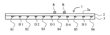
- FIG. 1A is a plan view illustrating a configuration example of a sensor chip of the biosensor according to the embodiment.
- 1B is a cross-sectional view of the sensor chip shown in FIG. 1A taken along line BB.
- the sensor chip 1 shown in FIG. 1A includes an insulating film 2 having a capturing surface 2a on which a capturing substance R is fixed, and a plurality of first electrode groups S1 to S6 provided on the side opposite to the capturing surface of the insulating film 2. And a plurality of second electrode groups D1 to D5.
- the capturing substance R is a substance that reacts with or binds to the biological substance to be measured.
- a specimen containing a biological substance to be measured is brought into contact with the capture surface 2a of the sensor chip 1.
- the combination of the biological substance to be measured and the capturing substance is not limited to a specific one.
- a protein (ligand) that reacts with a biomolecule (analyte) such as a pathogenic substance can be applied to the capture surface 2a as a capture substance.
- a variety of single-stranded DNAs with clear base sequences are placed on the capture surface 2a and the sample is reacted with them, only the portion of the base sequence complementary to the DNA sequence of the sample DNA strands bind.
- an antibody corresponding to the antigen to be measured can be applied to the capture surface 2a, and the antigen in the sample can be reacted with the antibody.
- the sensor chip in the present embodiment fixes a capturing substance on the capturing surface 2 a of the insulating film 2, and a plurality of sensor chips provided on the opposite side of the capturing surface 2 a through the insulating film 2. It is the structure which detects the change of the electric field by the to-be-measured substance trapped on the capture
- the first electrode groups S1 to S6 include a plurality of lines arranged side by side in one direction (left-right direction in FIG. 1A). Each line is formed so as to extend in a direction (vertical direction in FIG. 1A) perpendicular to the one direction. That is, the first electrode groups S1 to S6 include a plurality of lines parallel to each other.
- the second electrode groups D1 to D5 include a plurality of lines formed in a region between the first electrode groups S1 to S6.
- the lines of the second electrode groups D1 to D5 are arranged in the same direction as the direction in which the first electrode groups S1 to S6 are arranged, and extend in the same direction as the direction in which the first electrode groups S1 to S6 extend.
- the second electrode group includes a plurality of lines parallel to each other, and the plurality of lines are parallel to the first electrode groups S1 to S6. Also, none of the second electrode groups D1 to D5 is physically connected to any of the first electrode groups S1 to S6. For example, the first electrode S1 and the second electrode D1 adjacent to the first electrode S1 are insulated from each other and capacitively coupled.
- the line of the second electrode group D1 to D5 is adjacent to any line of the first electrode group S1 to S6. Thereby, when it sees from the direction perpendicular
- the capturing substance R is provided on the capturing surface 2a in a region between one line S4 of the first electrode group and the lines of the second electrodes D3 and D4 adjacent to the line S4.
- the capturing substance R captures the substance to be measured, and the first electrode
- the degree of change in capacitance between the second electrodes can be increased.
- the supplementary substance R can be provided at a position overlapping at least one of the first electrode and the second electrode.
- the supplementary substance R can be formed only at a position that overlaps at least one of the first electrode and the second electrode.
- the first electrode groups S1 to S6 and the second electrode groups D1 to D5 are provided on the surface of the substrate 3.
- the surface of the substrate 3 is covered with the insulating film 2, and the capturing substance R is fixed to the surface of the insulating film 2 opposite to the substrate 3. That is, the first electrode groups S1 to S6 and the second electrode groups D1 to D5 are provided between the laminated insulating film 2 and the substrate 3.
- the substrate 3 may be omitted, and the capturing material R may be provided on one surface of the insulating film 2, and the first electrode groups S1 to S6 and the second electrode groups D1 to D5 may be provided on the other surface. .
- the first electrode groups S1 to S6 and the second electrode groups D1 to D5 may not be in contact with the surface of the insulating film 2.
- a dielectric film may be further provided between the first electrode groups S 1 to S 6 and the second electrode groups D 1 to D 5 and the insulating film 2.
- each of the first electrode groups S1 to S6 is exposed on at least one side of the rectangular insulating film 2 and the substrate 3.
- One end of each of the second electrode groups D1 to D5 is also exposed on at least one side of the insulating film 2 and the substrate 3.
- An exposed portion of one end of each of the second electrode groups D1 to D5 serves as a terminal for connection to a drive unit (not shown) that inputs a drive signal to the second electrode groups D1 to D5.
- An exposed portion of one end of each of the first electrode groups S1 to S6 serves as a terminal for connection to a detection unit (not shown) that processes a signal output from the first electrode group in accordance with the drive signal. .
- the terminals of the first electrode groups S1 to S6 are provided on one side of the substrate 3 (lower side in FIG. 1A), and the second electrode groups D1 to D5 are provided on the side opposite to this side (upper side in FIG. 1A). Terminals are provided. In this way, by providing the terminals of the first electrode group and the terminals of the second electrode group on different sides of the insulating film 2, interference between the wiring drawn from the first electrode group and the wiring drawn from the second electrode group. Can be suppressed.
- the first electrode and the second electrode can be formed of a conductor such as Cu or ITO, for example.
- the insulating film 2 can be a cover film such as glass, PET, or acrylic. With this cover film, it can be set as the structure which covers the board
- a substance (ligant) that reacts with the substance to be detected (analyte) can be formed in a region between the first electrode and the second electrode in plan view.
- the sensor chip 1 can be made of a small piece of film and has a simple and inexpensive structure, so that it can be used as a disposable chip.
- the sensor chip can also be called a biochip or a biosensor.
- the sensor chip of the present embodiment has a configuration in which one surface of the planar or plate-like insulating film 2 is a capturing surface 2a, and a plurality of electrodes are arranged on the opposite side across the capturing surface 2a and the insulating film 2. is there. With this configuration, it is possible to accurately detect the measurement target substance captured by the planar capturing surface 2a by detecting the change in mutual capacitance between the plurality of electrodes. Further, the degree of freedom in designing the trapping substance R arrangement on the trapping surface 2a is increased.
- FIG. 2 is a configuration example of a biosensor system 10 to which the sensor chip 1 shown in FIG. 1 is connected.
- the biosensor system 10 shown in FIG. 2 includes a signal processing unit 4 connected to the first electrode groups S1 to S6 and the second electrodes D1 to D5 of the sensor chip 1.
- the signal processing unit 4 includes a driving unit 5 that inputs signals to the second electrode groups D1 to D5, and a detection unit 6 that processes signals from the first electrode groups S1 to S6.
- the first electrode groups S1 to S6 are connected to the signal processing unit 4 through lead wires 8s.
- the second electrode groups D1 to D5 are connected to the signal processing unit 4 through the lead wiring 8d.
- the lead wiring 8s and the like can be formed, for example, in a portion where the end portions of the first electrode groups S1 to S6 of the sensor chip 1 are exposed, that is, in an FPC connected to the terminal.
- the lead wiring 8d and the like can be formed, for example, in a portion where the ends of the second electrode groups D1 to D5 of the sensor chip 1 are exposed, that is, in an FPC connected to the terminal. Since drive signals are input to the second electrode groups D1 to D5, they can also be called drive lines. Since the first electrode groups S1 to S6 sense capacitance values, they can also be called sense lines.
- the signal processing unit 4 is connected to the calculation unit 7. Based on the signal processed by the detection unit 6, the calculation unit 7 generates data indicating the presence or amount of the biological substance to be measured or an image indicating the distribution of the biological substance on the capture surface.
- the signal processing unit 4 can be constituted by, for example, a semiconductor chip provided on a wiring board.
- the computing unit 7 can be configured by a computer having a processor and a memory, for example.
- the computer may be a general-purpose computer such as a personal computer or a server, or a dedicated computer incorporated in a measuring instrument.
- the hardware configurations of the signal processing unit 4 and the calculation unit 7 are not limited to specific ones. For example, at least a part of the drive unit 5, the detection unit 6, and the calculation unit 7 can be realized by a chip or a circuit formed on the substrate 3 of the sensor chip 1.
- the signal processing unit 4 connectable to the sensor chip 1 is the biosensor system 10, but a system including the sensor chip 1 and the signal processing unit 4 may be a biosensor system. Further, a system including the signal processing unit 4 and the calculation unit 7 can be a biosensor system. For example, a measuring instrument in which the signal processing unit 4 and the calculation unit 7 are mounted in one housing is one embodiment of the sensor system.
- the biosensor system can also be called a biosensor.
- the drive unit 5 inputs drive signals to the second electrode groups D1 to D5.
- the drive unit 5 can apply a pulse voltage to the second electrode groups D1 to D5 at a constant cycle.
- the detection unit 6 generates electrostatic capacitances formed between the second electrode groups D1 to D5 and the first electrode groups S1 to S6 based on signals output from the first electrode groups S1 to S6 according to the drive signals. The value of is detected.
- the detection unit 6 receives signals output from the first electrode groups S1 and S2 adjacent to the second electrode D1 at the timing when the drive signal is input to the second electrode D1.
- the detection unit 6 detects a signal indicating a change in charge of the first electrodes S1 and S2 when a drive signal is input to the second electrode D1.
- the detection unit 6 uses this signal to determine the value indicating the capacitance between the first electrode S1 and the second electrode D1 and the capacitance between the first electrode S2 and the second electrode D1. The value shown is obtained.
- the static of the first electrode S4 and the second electrode D3 corresponding to the region where the capturing substance R that captured the biological substance is provided.
- the capacitance and the capacitance of the first electrode S4 and the second electrode D4 change. Therefore, the signal from the first electrode S4 changes. Further, the capacitance of the first electrode S3 and the second electrode D3 corresponding to the region where the capturing material R is not provided, and the first electrode S4 and the second electrode corresponding to the region where the capturing material R is provided. The difference from the capacitance of the electrode D3 is increased.
- the detection unit 6 can detect a change in capacitance from changes in signals output from the first electrode groups S1 to S6. Based on the change in capacitance detected by the detection unit 6, the calculation unit 7 can generate data indicating the presence, amount, or distribution of the biological substance to be measured.
- the detection unit 6 calculates, for example, the difference between the signals output between two adjacent first electrodes in the first electrode group, thereby obtaining the capacitance between the two first electrodes. A difference value can be obtained.
- the calculation unit 7 uses the difference value of the capacitance between the two second electrodes to indicate the presence or amount of the biological substance to be measured captured on the capture surface 2a or the biological material on the capture surface 2a. It is possible to generate an image showing the distribution of.
- the signals output from the first electrode groups S1 to S6 may include various noise components in addition to the components of the capacitance change due to the capturing substance R capturing the biological substance to be measured. . Therefore, the detection unit 6 can acquire a difference signal between the two first electrodes. Thereby, a noise component can be removed from the output signal. In particular, the noise component can be removed from the signal of the first electrode by taking the difference between the adjacent first electrodes, which often have high noise correlation.
- two types of electrodes responsible for sensing and driving that is, the first electrode groups S1 to S6 and the second electrode groups D1 to D5 are formed under the insulating film 2.
- a trapping substance for example, a ligand
- the capturing substance is provided at a position between the first electrode and the second electrode in plan view.
- the sensor chip 1 as described above is connected to the signal processing unit 4.
- FIG. 3A is a plan view showing a modified example of the arrangement of the capturing substance R on the capturing surface 2a of the sensor chip 1.
- FIG. 3B is a cross-sectional view of the sensor chip 1 shown in FIG. 3A.
- different capturing substances R1 and R2 are fixed to two different regions on the capturing surface 2a. That is, different partial structures are formed as the capturing substances R1 and R2 provided on the capturing surface 2a. That is, the biological substance that reacts or binds to the capturing substance R1 is different from the biological substance that reacts or binds to the capturing substance R2.
- the trapping substance R1 is provided between the second electrode D1 and the first electrode S2 and between the first electrode S2 and the second electrode D2.
- a trapping substance R2 is provided between the second electrode D3 and the first electrode S4 and between the first electrode S4 and the second electrode D4.
- FIG. 4A is a cross-sectional view illustrating an example of a connection form of the sensor chip.
- the sensor chip 1 is placed on the table 21 including the extraction electrode pads 22.
- a lead electrode pad 22 is connected to a portion of the side surface of the sensor chip 1 placed on the table 21 where the first electrode S1 is exposed.
- the probe 23 is provided in a state in which contact and separation are possible with respect to the extraction electrode pad 22.
- the probe 23 is electrically connected to the signal processing unit 4.
- a lead electrode pad 22 is also provided on the side surface of the sensor chip 1 where the second electrode D1 is exposed.
- the extraction electrode pad 22 is connected to the second electrode D1 of the sensor chip 2 placed on the table 21.
- the probe 23 is also provided in a state in which contact and separation are possible with respect to the lead electrode pad 22 to which the second electrode D1 is connected.
- FIG. 4B is a cross-sectional view showing another example of the connection form of the sensor chip.
- the sensor chip 1 is provided with the insulating film 2 so that a part of the first electrode S1 and the second electrode 2 provided on the substrate 3 is exposed. That is, the first electrode S1 and the second electrode D1 extend to a portion where the insulating film 2 does not cover the substrate 3.
- the probe 23 With the sensor chip 1 fixed on the table 21, the probe 23 is brought into contact with the exposed portion of the first electrode S1 and the second electrode D1 on the substrate 3, whereby the first electrode of the sensor chip 1 is contacted.
- the group S and the second electrode group D are connected to the signal processing unit 4.
- the detection unit 6 determines the presence or amount of a biological substance captured by the capturing substance R1 based on the capacitance value detected by the first electrode S2, and is detected by the first electrode S4.
- the presence or amount of the biological substance captured by the capturing substance R2 can be determined based on the capacitance value.
- FIG. 5 is a flowchart showing an operation example of the biosensor system in the present embodiment.
- the sensor chip in the initial state is connected to the signal processing unit 4 (Op01).
- the sensor chip in the initial state is an unused sensor chip before contacting the specimen.
- the calculation unit 7 When the calculation unit 7 detects the sensor chip connection in the initial state, the calculation unit 7 issues a command to the drive unit 5 and the detection unit 6 to acquire the value of the capacitance between the first electrode and the second electrode. Thereby, the detection part 6 acquires the electrical capacitance signal which shows the value of the electrostatic capacitance in the sensor chip of an initial state (Op02).
- the drive unit 5 applies a drive signal voltage to the second electrode groups D1 to D5.
- the detection unit 6 acquires the voltages of the first electrode groups S1 to S6 while applying the drive signal voltage as electric capacitance signals.
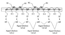
- FIG. 6A is a diagram showing an example of a part of electric lines of force when driving the sensor chip 1 in the initial state and signals output from the first electrode groups S1 to S6.
- the density of the lines of electric force at the places where the capturing substance R1 and the capturing substance R2 are provided is higher than that at the place where the capturing substance is not provided.
- the capacitance values detected by the first electrode groups S1 to S6 are ⁇ 1 to ⁇ 6, respectively, between adjacent first electrodes detected before the drop of the sample of Op02.
- the difference signals are Signal1 (before) to Signal5 (before).
- the detection unit 6 can output these differential signals.
- Singal1 (before) is calculated by ⁇ 2- ⁇ 1.
- the specimen is dropped onto the capturing surface 2a of the sensor chip 1 (Op03).
- the capture surface 2a is cleaned to remove excess sample.
- the sample may be dropped on the capture surface 2a using a dropper, or the sample may be sent to a flow path formed in advance on the capture surface 2a.
- the cleaning is performed, for example, by supplying a cleaning liquid to the capturing surface 2a for a predetermined time.
- the calculation unit 7 issues a command to the drive unit 5 and the detection unit 6 to acquire the capacitance value between the first electrode and the second electrode. Thereby, the detection part 6 acquires the electrical capacitance signal after dripping a sample (Op04).
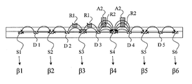
- FIG. 6B is a diagram illustrating an example of a part of the electric lines of force when the sensor chip 1 is driven after the sample is dropped and signals output from the first electrode groups S1 to S6.
- the density of the electric lines of force at the location where the capturing substance R1 bound to the biological substance (analyte) A1 to be measured and the capturing substance R2 bound to the analyte A2 are provided. It is higher than the location where the capture substances R1 and R2 are not provided, and is higher than before the sample is dropped (see FIG. 6A). As shown in FIG.
- the capacitance values detected by the first electrode groups S1 to S6 are ⁇ 1 to ⁇ 6, respectively, between the adjacent first electrodes detected after the drop of the specimen of Op03, that is, , S1 to S2, S2 to S3, S3 to S4, S4 to S5, and S5 to S6 are differential signals from Signal1 (after) to Signal5 (after), respectively.
- the detection unit 6 can output these differential signals.
- Singal1 (after) is calculated by ⁇ 2- ⁇ 1.
- the calculation unit 7 can determine the presence or absence of the analyte corresponding to the trapping substance R1 based on the values of ⁇ Signal1 and ⁇ Signal2.
- the values of ⁇ Signal3 and ⁇ Signal4 shown in the above formulas (4) and (5) are not 0, and vary depending on the amount or state of the analyte A2.
- the presence or amount of the analyte A2 corresponding to the trapping substance R2 can be determined from the values of ⁇ Signal3 and ⁇ Signal4. For example, when the values of ⁇ Signal1 and ⁇ Signal2 exceed the threshold value, the calculation unit 7 can determine that the analyte corresponding to the trapping substance R1 has been detected. Alternatively, the calculation unit 7 can calculate a value indicating the amount of the analyte A1 by using the value of ⁇ Signal1 and the value of ⁇ Signal2.
- the above is an example of the operation in which the biosensor system 10 detects the measurement target substance from the change in the capacitance value after capturing the measurement target substance and the initial capacitance value.
- the difference between the capacitance values of two adjacent first electrodes is detected. Therefore, a noise component common to the two first electrodes, for example, a noise component due to the environment of the entire capture surface 2a is removed. Furthermore, the difference between the capacitance value before contact with the specimen and the capacitance value after contact is detected. Thereby, noise components due to the local environment of the capturing surface 2a such as dust on the capturing surface 2a and the supplementary substance R are removed. By combining these difference detections, it is possible to detect a change in capacitance caused by a biological substance with higher accuracy.
- FIG. 7 is a flowchart showing another operation example of the biosensor system.
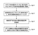
- the sensor chip 1 in the initial state is connected to the signal processing unit 4 (Op11).
- the capture surface 2a of the sensor chip 1 includes a region where a ligand, which is an example of a capture substance, is formed, and a region where no ligand is formed.
- the specimen is dropped on the capturing surface 2a of the sensor chip 1 in the initial state (Op12). After the sample is dropped, the capture surface 2a is cleaned to remove excess sample. It may take time for the movement of the specimen to stabilize on the capture surface 2a.
- the drive unit 5 applies a drive voltage to the second electrode groups D1 to D5 at a constant cycle, and the detection unit 6 monitors the output signals of the first electrode groups S1 to S6 at the same cycle.
- the biosensor system 10 can continue the above-described operation until the value of the signal detected by the detection unit 6 is stabilized. For example, when the fluctuation range of the value detected by the detection unit 6 becomes smaller than the threshold value, it can be determined that the fluctuation of the capacitance is stable.
- the detection unit 6 can determine the value of the capacitance based on the signal detected after the fluctuation of the capacitance is stabilized.
- the calculation unit 7 sends the value of the capacitance between the first electrode and the second electrode to the drive unit 5 and the detection unit 6. Issue an instruction to get Thereby, the detection part 6 acquires the electrical capacitance signal which shows the value of the electrostatic capacitance between the 1st electrode and 2nd electrode after dripping a sample and being stabilized (Op13).
- the drive unit 5 applies a drive signal voltage to the second electrode groups D1 to D5.
- the detection unit 6 acquires the voltages of the first electrode groups S1 to S6 while applying the drive signal voltage as electric capacitance signals.
- FIG. 8 is a diagram showing an example of a part of electric lines of force when the sensor chip 1 is driven after the sample is dropped and signals output from the first electrode groups S1 to S6.
- the density of the lines of electric force at the places where the capturing substance R1 and the capturing substance R2 are provided is higher than that at the place where the capturing substance is not provided.
- the capacitance values detected by the first electrode groups S1 to S6 are ⁇ 1 to ⁇ 6, respectively, the difference between the adjacent first electrodes detected after the Op13 sample is dropped.
- the signals are Signal1 (after) to Signal5 (after).
- the detection unit 6 can output these difference signals as signal values.
- Singal1 (after) is calculated by ⁇ 2- ⁇ 1.
- the calculation unit 7 is detected in the region where the ligands R1 and R2 that are the capturing substances are formed, based on the signal value detected in the region where the capturing substance is not formed.
- the signal value is evaluated (Op14). This makes it possible to determine the presence or amount of the analytes A1 and A2 to which the ligands R1 and R2 react or bind. For example, in the example shown in FIG. 8, the capacitance values ⁇ 1, ⁇ 2, ⁇ 3, ⁇ 5, and ⁇ 6 detected in the region where the ligand is not formed are almost equal.
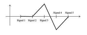
- FIG. 9 is a graph showing Signal 1 (after) to Signal 5 (after) calculated by the above formulas (7) to (11).
- the calculation unit 7 uses the signal values Signal1 (after) and Signal2 (after) in the region where the ligand R1 is formed, based on Signal5 (after) which is the signal value detected in the region where the capturing substance is not formed. evaluate. Thereby, the presence or absence or amount of the analyte corresponding to the ligand R1 can be determined.
- the calculation unit 7 evaluates the signal values Signal3 (after) and Signal4 (after) in the region where the ligand R2 is formed, using Signal5 (after) as a reference.
- the calculation unit 7 can determine the difference between the reference value of Signal 5 and each of Signals 1 to 4 (after), and can determine the presence or absence of the analyte based on the magnitude of the difference. In this way, the measurement target substance can be detected from the difference between the capacitance value in the region where the capturing substance is not formed and the capacitance value in the region where the capturing substance is formed.
- the above example is an example of the operation of detecting the substance to be measured from the difference between the capacitance of the region where the capturing structure is formed on the capturing surface 2a and the capacitance value of the region where the capturing structure is not formed. is there.
- the difference between the capacitance values of the two adjacent first electrodes is detected, and further, the capacitance value in the region where the trapping substance is present and the capacitance value in the region where the trapping substance is not present
- the difference is also detected.
- the detection unit 6 may detect a difference in capacitance value between a region where the supplementary substance is provided and a region where the capture substance is not present before and after contact with the specimen. By combining these differences, a more accurate capacitance can be obtained.
- the detection unit 6 can further decode the capacitance value of each of the first electrodes by using the difference between the values of the two first electrodes.
- the capacitance values ⁇ 2, ⁇ 3, and ⁇ 4 of the first electrodes S2, S3, and S4 are decoded based on the capacitance value ⁇ 5 of the first electrode S5 in the region where the trapping substance R is not provided. can do.
- the difference between the capacitance values ⁇ 3, ⁇ 4, ⁇ 5 of the first electrodes S2, S3, S4 and the capacitance value ⁇ 5 of the first electrode S5 can be calculated by the following equations (12) to (14).
- ⁇ 5- ⁇ 4 Signal 4 (after) (12)
- ⁇ 5- ⁇ 3 Signal 4 (after) + Signal 3 (after) (13)
- ⁇ 5- ⁇ 2 Signal 4 (after) + Signal 3 (after) + Signal 2 (after) (14)
- the computing unit 7 uses the decoded capacitance values of the first electrodes S2, S3, and S4 to determine the presence / absence or amount of the measurement target substance, or generate data indicating the distribution of the measurement target substance on the capture surface 2a. be able to.
- the detection unit 6 or the calculation unit 7 uses the difference value between the output signals of the two first electrodes, and the capacitance value of one first electrode of the first electrode groups S1 to S6 and the other first electrodes. The difference from the capacitance value of one electrode group can be calculated. Thereby, data indicating the distribution of capacitance values on the capture surface 2a is obtained.
- the calculation unit 7 can generate an image showing the distribution of capacitance values on the capture surface 2a.
- FIG. 10A and 10B are diagrams for explaining an operation example 3.
- FIG. 10A is a diagram illustrating an example of mutual capacitance values measured in advance in a predetermined environment for use in calibration.
- ⁇ 2a is measured in advance in a predetermined environment and recorded as calibration data.
- the predetermined environment is not particularly limited, but for example, the measurement can be performed in an environment where there is little capacitance value noise.
- FIG. 10B is a diagram illustrating an example of the mutual capacitance value detected by the detection unit 6 after the specimen is supplied to the sensor chip 1.
- the analyte is not captured in the capturing material R1
- the analyte A2 is captured in the capturing material R2.
- the calculation unit 7 calculates the difference ⁇ 3- ⁇ 2 between the mutual capacitance value of the region where the capturing substance R1 is formed and the mutual capacitance value of the region where there is no capturing material.
- the calculation unit 7 calculates the difference ⁇ 4- ⁇ 2 between the mutual capacitance value in the region where the capturing material R2 is formed and the mutual capacitance in the region where the capturing material is not present.
- the capacitance values ( ⁇ 3- ⁇ 2) ( ⁇ 4- ⁇ 2) obtained by these measurements can be calibrated using the calibration data ⁇ 2a, ⁇ 3a, ⁇ 4a recorded in advance.
- the computing unit 7 can determine the presence or absence of an analyte by comparing ( ⁇ 3- ⁇ 2) with calibration data ( ⁇ 3a- ⁇ 2a).
- the calculation unit 7 calculates the difference between ( ⁇ 3 ⁇ 2) and ( ⁇ 3a ⁇ 2a), and can determine whether or not the analyte is detected based on the magnitude of the difference. For example, in the example shown in FIG. 10B, the calculation unit 7 can determine that there is no analyte when ⁇ 3- ⁇ 2 ⁇ 3a- ⁇ 2a, and can determine that there is an analyte when ⁇ 4- ⁇ 2> ⁇ 4a- ⁇ 2a. it can.
- the detection accuracy can be further improved by using the capacitance value of the measurement data and the capacitance value of the calibration data.
- the capacitance values ⁇ 1 to ⁇ 5 after sample supply can be normalized using the capacitance values ⁇ 1a to ⁇ 5a of the calibration data, respectively.
- FIGS. 11A to 11E Next, an example of a manufacturing process of the sensor chip will be described with reference to FIGS. 11A to 11E.
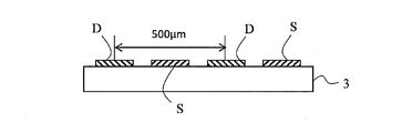
- Cu is pattern-deposited with a thickness of 5 ⁇ m using a mask.
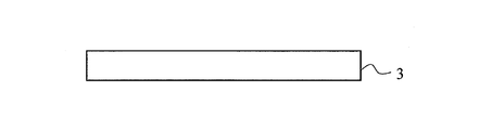
- the first electrode S and the second electrode D are formed on the glass substrate 3.
- the pitch of the second electrodes D is set to 500 ⁇ m.
- SiO 2 is deposited on the glass substrate 3 so as to cover the first electrode S and the second electrode D with a thickness of 50 ⁇ m. Thereby, the insulating film 2 is formed.
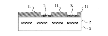
- a part of the surface of the insulating film 2 is covered with a mask 11, and a ligand R, which is an example of a trapping substance, is fixed to a portion not covered with the mask 11.
- a ligand R which is an example of a trapping substance
- Various methods can be used to immobilize the ligand R.
- there is a method of immobilizing a ligand by introducing a modifying group on the surface of the insulating film 2 and reacting with a reactive group of the ligand to generate a covalent bond.
- the modifying group can be introduced by masking a part of the surface of the insulating film 2 and immersing in a silane coupling agent for a predetermined time.
- modifying group at least one modifying group selected from the group consisting of an amino group, a carboxyl group, an epoxy group, an aldehyde group, a thiol group, an isocyanate group, and an isothiocyanate group can be introduced.
- These modifying groups react with thiol groups, amino groups, carboxyl groups, hydroxyl groups, etc. that the ligand has (which may be inherent to the ligand or previously introduced by a predetermined operation) to form a covalent bond.
- the ligand having a reactive group include proteins, polypeptides, nucleic acids, and sugars.
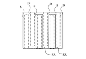
- FIG. 12 is a diagram illustrating an example of a region where the ligand R is formed.
- a solid line RR indicates a ligand formation region.
- a ligand is formed in a region overlapping the first electrode S and a region between the first electrode 2 and the adjacent second electrode.
- 13A, 13B, 14A to 14D, and 15 are diagrams for explaining another example of the manufacturing process of the sensor chip.
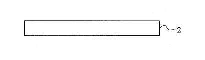
- 13A and 13B show a manufacturing process of the substrate 3 on which the first electrode S and the second electrode D are formed.
- Cu is pattern-deposited with a thickness of 5 ⁇ m using a mask.
- the first electrode S and the second electrode D are formed on the PET substrate 3.
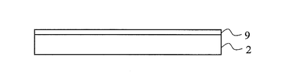
- an Al 2 O 3 film 9 is deposited with a thickness of 10 ⁇ m (FIG. 14B).
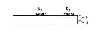
- FIG. 14C a part of the surface of the Al 2 O 3 film 9 is covered with a mask 11, and a ligand R, which is an example of a trapping substance, is fixed to a part not covered with the mask 11. Is done.
- the mask 11 is removed.
- FIG. 14D the surface on which the ligand R of the Al 2 O 3 film 9 is formed becomes the trapping surface 2a.
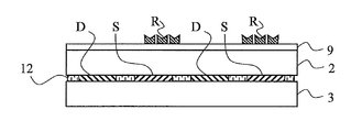
- the PET substrate 3 shown in FIG. 13B and the PET substrate 2 shown in FIG. 14D are bonded together using an adhesive or an adhesive tape (OCA or the like).
- OCA adhesive or the like
- the surface opposite to the surface to be provided is bonded by the adhesive 12.
- FIG. 16 is a plan view showing a modified example of the configuration of the sensor chip.
- 17 is a cross-sectional view of the sensor chip shown in FIG. 16 taken along line LL.
- FIG. 18 is an enlarged view near the intersection of the first electrode S3 and the second electrode D3 of the sensor chip shown in FIG.
- FIG. 19 shows a modification of the configuration of the portion shown in the enlarged view of FIG.
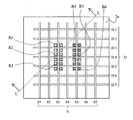
- the first electrode group S is formed by a plurality of lines S1 to S7 arranged at equal intervals.
- a second electrode group D is formed by a plurality of lines D1 to D7 intersecting these first electrode groups S1 to S7 in plan view.
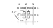
- the trapping substance R1 is provided at four corners formed by the intersections of the first electrode S3 and the second electrode D3. Specifically, as shown in FIG.
- a trapping substance R1 is arranged.
- the trapping substance R2 is formed at the four corners formed by the intersections of the first electrode S3 and the second electrode D4, and the four corners formed by the intersections of the first electrode S3 and the second electrode D5.
- the trapping substance R3 is formed at the four corners formed by the intersections of the first electrode S5 and the second electrode D3
- the trapping substance R5 is formed at the four corners formed by the intersections of the first electrode S5 and the second electrode D4.
- the trapping substances R6 are provided at the four corners formed by the intersections of the first electrode S5 and the second electrode D5, respectively.
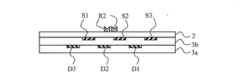
- the second electrode groups D1 to D7 are formed on the substrate 3a.
- An insulating layer 3b is provided on the substrate 3b so as to cover the second electrode groups D1 to D7.
- First electrode groups S1 to S7 are formed on the insulating layer 3b covering the substrate 3a. That is, the second electrode groups D1 to D7 and the first electrodes S1 to S7 are formed in different layers with the insulating layer 3a interposed therebetween. Thereby, it can arrange
- the first electrode group S and the second electrode group D may be formed in the same layer, and an insulator may be formed between the first electrode and the second electrode at a portion where they intersect. Specifically, a bridge in which one of the first electrode and the second electrode straddles the other may be formed.
- the capturing substance R1 is formed at a position overlapping the intersection of the first electrode S3 and the second electrode D3 in plan view.
- the trapping substance R1 is disposed so as to overlap the four corner portions formed by the intersections of the first electrode and the second electrode in plan view. These four corner portions are regions where capacitance is formed between the first electrode and the second electrode.
- the capacitance value detected by the first electrode is likely to reflect the capacitance components at the four corners. Therefore, the measurement target substance captured by the capturing substance R1 is easily reflected in the capacitance value detected by the first electrode.
- the drive unit 5 sequentially supplies drive pulse (drive pulse) signals to the plurality of second electrodes D1 to D7.
- drive pulse By this drive pulse signal, an electric field is generated between the first electrode group S and the second electrode group D.
- a capacitance is generated near the intersection of the first electrode and the second electrode.
- the capacitance change in the vicinity of the intersection is detected by the detector 6 as an output signal from each line of the plurality of first electrodes S1 to S7. Thereby, it is possible to detect the position (coordinates) where the capacity has changed due to the substance captured by the capturing substance R on the capturing surface 2a.
- the sequential drive method is used, but it is also possible to adopt a method in which a weighted drive (drive) signal is supplied to each of a plurality of electrodes a plurality of times.
- drive signals generate an electric field between the first electrode group S and the second electrode group D.
- a capacitance is generated near the intersection of the first electrode and the second electrode.
- the capacity near the intersection changes.
- the capacitance change in the vicinity of the intersection is detected by the detector 6 as an output signal from each line of the plurality of first electrodes S1 to S7.
- a plurality of output signals are subjected to arithmetic processing by the arithmetic unit 7, and a position (coordinates) where the capacity has changed due to the substance captured by the capturing substance R on the capturing surface 2 a can be detected.
- Each of the second electrode groups D1 to D7 is inputted with a plurality of weighted drive signals at the same time, and the output signals of the first electrode groups S1 to S7 with respect to the drive signals are detected and calculated.
- Information indicating a change in capacity can be obtained. That is, by detecting the output signals of the first electrode groups S1 to S7 a plurality of times at the same time, it is possible to obtain the capacitance value at the position (each node) corresponding to each intersection of the capturing surface 2a. Can be obtained.
- the supplementary substance R can be arranged at each intersection of the first electrode and the second electrode on the capture surface 2a, a wider variety of supplementary substances R can be arranged. As a result, a wide variety of substances to be measured can be efficiently detected by scanning or simultaneously driving the second electrode group.
- different supplementary substances are arranged for each intersection of the first electrode and the second electrode, but the same supplementary substance can be arranged over a plurality of intersections.
- FIG. 20 is a plan view showing a modification of the configuration of the sensor chip.
- 21 is a cross-sectional view of the sensor chip shown in FIG. 20 taken along line LL.
- FIG. 22 shows a modification of the configuration shown in FIG.
- the first electrodes S1 to S3 include a plurality of first electrode pads Sa arranged in the first direction and a plurality of first connection wirings Sb connecting the plurality of first electrode pads Sa.
- the second electrode groups D1 to D3 include a plurality of second electrode pads Da arranged in the second direction, and a second connection wiring Db connecting the plurality of second electrode pads Da.
- the first electrode pad Sa has a shape with the narrowest width at both ends connected to the first connection wiring Sb and the widest width at the center.
- the second electrode pad Da is also narrowest at both ends connected to the second connection wiring Db and is widest at the center.
- the portion of the first connection wiring Sb having the narrowest width in the first electrode and the portion of the second connection wiring Db having the narrowest width in the second electrode are arranged to intersect each other. Therefore, the first electrode pad Sa is adjacent to the four second electrode pads Da, and the second electrode pad Da is also adjacent to the four first electrode pads Sa. That is, the first electrode pad Sa has four sides, and each of these four sides faces one side of the four adjacent second electrode pads Da.
- the second electrode pad Da also has four sides, and these four sides respectively face one side of the four first electrode pads Sa.
- both the first electrode pad Sa and the second electrode pad Da can be diamond-shaped or square.
- the trapping substance R1 is between the side near the intersection of the first electrode pad Sa adjacent to the intersection of the first electrode S2 and the second electrode group D2 and the side of the adjacent second electrode pad Da facing this side. It is formed to straddle.
- the region sandwiched between the first electrode pad Sa and the second electrode pad Da where the trapping substance R1 is formed is a region where the capacitance between the first electrode S2 and the second electrode D2 is formed. Therefore, the measurement target substance captured by the capture substance R1 is easily reflected in the capacitance value detected by the second electrode.
- the area of the electrode can be increased by the first electrode pad Sa and the second electrode pad Da. This increases the sensitivity of the sensor. Therefore, the detection accuracy can be further increased.
- the second electrode groups D1 to D3 are formed on the substrate 3a.
- First electrodes S1 to S3 are formed on an insulating layer 3b covering the substrate 3a. That is, the second electrode groups D1 to D3 and the first electrodes S1 to S3 are formed in different layers with the insulating layer 3b interposed therebetween.
- the second electrode groups D1 to D3 and the first electrodes S1 to S3 are formed in the same layer, and an insulator is inserted between the first electrode and the second electrode at a portion where they intersect. You can also.
- the position overlapping the intersection of the first electrode S3 and the second electrode D3 in plan view, and the side of the first electrode pad Sa and the side of the second electrode pad Da that surround the intersection are opposed to each other.
- the capturing substance R1 is formed at both positions overlapping the region to be captured.
- the driving unit 5 sequentially supplies drive pulse signals to the plurality of second electrode groups D1 to D3.
- the drive pulse signal generates an electric field between the first electrode Sa and the second electrode Da adjacent to each other.
- the electric field between the first electrode pad Sa and the second electrode pad Da changes.
- the capacitance between the first electrode and the second electrode at each intersection changes.
- the sequential drive method is used, but it is also possible to adopt a method in which a weighted drive (drive) signal is supplied to each of a plurality of electrodes a plurality of times.
- a weighted drive (drive) signal is supplied to each of a plurality of electrodes a plurality of times.
- drive signals an electric field is generated between the first electrode pad of the first electrode group S and the second electrode pad of the second electrode group D adjacent thereto.
- a capacitance is generated near the intersection of the first electrode and the second electrode.
- the capacity near the intersection changes.
- the capacitance change in the vicinity of the intersection is detected by the detector 6 as an output signal from each line of the plurality of first electrodes S1 to S7.
- a plurality of output signals are subjected to arithmetic processing by the arithmetic unit 7, and a position (coordinates) where the capacity has changed due to the substance captured by the capturing substance R on the capturing surface 2 a can be detected.
- Each of the second electrode groups D1 to D7 is inputted with a plurality of weighted drive signals at the same time, and the output signals of the first electrode groups S1 to S7 with respect to the drive signals are detected and calculated.
- Information indicating a change in capacity can be obtained. That is, by detecting the output signals of the first electrode groups S1 to S7 a plurality of times at the same time, it is possible to obtain the capacitance value at the position (each node) corresponding to each intersection of the capturing surface 2a. Can be obtained.
- FIG. 23 is a plan view showing a modified example of the configuration of the sensor chip.
- 24 is a cross-sectional view of the sensor chip shown in FIG. 23 taken along line LL.
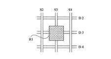
- the capturing substance R1 and the capturing substance R2 are both formed in regions overlapping the plurality of first electrode groups S and the plurality of second electrode groups D.
- the capturing substance R1 is integrally formed in a region that overlaps all the intersections of the first electrodes S2 to S4 and the second electrode groups D2 to D7.
- the trapping substance R2 is integrally formed in a region that overlaps all the intersections of the first electrodes S5 to S7 and the second electrode groups D2 to D7.
- the capturing substance R1 and the capturing substance R2 are formed in different regions of the capturing surface 2a.
- FIG. 25 is a cross-sectional view showing a modified example of the configuration of the sensor chip.
- the second electrode groups D1 to D6 are formed on the surface of the substrate 3a.
- An insulating layer 13a is provided so as to cover the surface of the substrate 3a on which the first electrode groups D1 to D6 are formed.
- a heat dissipation layer 14a is provided on the insulating layer 13a.
- a substrate 3b is provided on the heat dissipation layer 14a, and first electrodes S1 to S7 are provided on the surface of the substrate 3b.
- An insulating layer 13b and a heat dissipation layer 14b are sequentially provided on the surface of the substrate 3b.
- the insulating film 2 having the capturing surface 2a is provided on the heat dissipation layer 14b.
- the heat radiation layers 14a and 14b are preferably formed of a material having high thermal conductivity.
- the heat dissipation layers 14a and 14b can be formed of mesh metal.
- the heat dissipation layers 14a and 14b are insulated from the first electrode groups S1 to S7 and the second electrode groups D1 to D6 by the insulating layers 13a and 13b.
- a heat dissipation structure using the heat dissipation layers 14a and 14b may be provided in a part of the region where the first electrode groups S1 to S7 and the second electrode groups D1 to D7 are formed.
- a signal detected in the region having the heat dissipation structure can be used for calibration.
- settings of various parameters such as a parameter for converting an electric signal detected by the first electrode S into a capacitance value can be appropriately corrected according to the temperature.
- the influence of environmental changes such as temperature at the time of parameter initialization and measurement can be reduced by calibration.
- a material having high thermal conductivity can be connected to the end opposite to the terminal where the first electrode S and the second electrode are connected to the signal processing unit 4. .
- the number of the first electrodes S and the second electrodes D in the above example is an example, and is not limited to the above example.
- a driving signal may be input to the first electrode S and the signal of the second electrode D may be detected.
- the materials of the insulating film 2 and the substrate 3 are not limited to those mentioned in the above example.
- the insulating film 2 and the substrate 3 do not need to have a high visible light transmittance.
- the capture surface 2a can be appropriately selected or appropriately processed according to the properties of the substance to be measured.
- the insulating film 2 may be made of a hydrophilic material. Moreover, you may give the process which forms an unevenness
- the capture substance for example, a substance having a partial structure of a molecule corresponding to the measurement target substance can be formed on the capture surface 2a.
- an antibody corresponding to the antigen to be captured may be formed on the capture surface 2a as a capture substance.
- a substance used for adsorbing, capturing, or identifying a measurement object can be formed on the capturing surface 2a as a capturing substance.
- the biosensor as an embodiment of the present invention includes a sensor chip and a system form including a sensor chip and a circuit or processor for controlling the sensor chip and processing a signal from the sensor chip.
- a biosensor system including a sensor chip and a signal processing unit, and a biosensor system in which a signal processing unit and a calculation unit are combined with the sensor chip are also included in the embodiments of the present invention.
Landscapes
- Health & Medical Sciences (AREA)
- Immunology (AREA)
- Life Sciences & Earth Sciences (AREA)
- Chemical & Material Sciences (AREA)
- Engineering & Computer Science (AREA)
- Pathology (AREA)
- Biomedical Technology (AREA)
- Hematology (AREA)
- General Physics & Mathematics (AREA)
- Molecular Biology (AREA)
- Urology & Nephrology (AREA)
- Analytical Chemistry (AREA)
- General Health & Medical Sciences (AREA)
- Biochemistry (AREA)
- Physics & Mathematics (AREA)
- Cell Biology (AREA)
- Medicinal Chemistry (AREA)
- Food Science & Technology (AREA)
- Microbiology (AREA)
- Biotechnology (AREA)
- Chemical Kinetics & Catalysis (AREA)
- Electrochemistry (AREA)
- Investigating Or Analyzing Materials By The Use Of Electric Means (AREA)
- Apparatus Associated With Microorganisms And Enzymes (AREA)
Abstract
生体由来物質の高精度な検出を可能にする。センサチップは、測定対象の生体由来物質と反応または結合する捕捉用物質が固定された捕捉面(2a)を有する絶縁膜(2)と、絶縁膜(2)の捕捉面(2a)とは反対側に設けられ、少なくとも1つの方向に並んで設けられる複数の電極群(S1~S6、D1~D5)とを有する。補足用物質(R)は、捕捉面(2a)において、平面視で、複数の電極と重なる領域又は、前記複数の電極のうち少なくとも2つの電極で挟まれる領域の少なくともいずれかに形成される。
Description
本願開示は、検体中の生体由来物質を電気的に検知する技術に関する。
従来、センサを用いて検体中の抗原を電気感知する方法が提案されている(例えば、特開2010-160151号公報参照)。また、この特開2010-160151号公報では、2つの電極の少なくとも一方の表面に、抗原に対し特異的結合反応性を有する抗体層を固定することが開示されている。この抗体が抗原を捕捉することによる2電極間の導電特性の変化が、抗原の電気感知の指標となる。
上記従来技術のように、電極表面に抗体層を塗ると、電極の酸化及び汚れが判定結果に影響しやすい。そのため、検出精度が落ちやすい。そこで、本願は、生体由来物質の高精度な検出を可能にするバイオセンサを開示する。
本願開示のセンサチップは、測定対象の生体由来物質と反応または結合する捕捉用物質が固定された捕捉面を有する絶縁膜と、前記絶縁膜の前記捕捉面とは反対側に設けられ、少なくとも1つの方向に並んで設けられる複数の電極とを備える。前記補足用物質は、前記捕捉面において、平面視で、前記複数の電極と重なる領域又は、前記複数の電極のうち少なくとも2つの電極で挟まれる領域の少なくともいずれかに形成される。
本願開示によれば、生体由来物質の高精度な検出を可能にするバイオセンサが実現できる。
本発明の一実施形態に係るセンサチップは、測定対象の生体由来物質と反応または結合する捕捉用物質が固定された捕捉面を有する絶縁膜と、前記絶縁膜の前記捕捉面とは反対側に設けられ、少なくとも1つの方向に並んで設けられる複数の電極とを備える。前記補足用物質は、前記捕捉面において、平面視で、前記複数の電極と重なる領域又は、前記複数の電極のうち少なくとも2つの電極で挟まれる領域の少なくともいずれかに形成される。
上記構成によれば、測定対象の生体由来物質を捕捉する捕捉面を有する絶縁膜の捕捉面とは反対側に設けられた複数の電極の間の静電容量の値を検出することができる。この複数の電極との間の静電容量の値は、絶縁膜の捕捉面における電界の状態を反映したものとなる。捕捉面の一部において捕捉用物質が測定対象の生体由来物質と反応または結合した場合、その生体由来物質の周りの電界が変化する。この電界の変化は、検出される静電容量の値に反映される。上記静電容量の値を検出することで、捕捉面における生体由来物質の位置や量を検出することができる。ここで、捕捉用物質が固定される捕捉面と複数の電極との間には絶縁膜が設けられるので、電極の酸化又は汚れが検出精度に与える影響が小さくなる。また、すくなくとも1つの方向に並んで設けられる複数の電極により、捕捉面の複数の箇所で形成される静電容量の値を検出できるので、捕捉面上の微妙な電位の変化を検出することが可能になる。その結果、生体由来物質の高精度な検出が可能になる。
ここで、絶縁膜の前記捕捉面とは反対側に設けられる複数の電極の形態は、絶縁膜の捕捉面とは反対側の面に接触するように複数の電極が形成される場合に限られない。例えば、捕捉面を有する絶縁膜の前記捕捉面とは反対側の面と複数の電極との間に、少なくとも1つのさらなる絶縁膜を設けることもできる。また、捕捉面を有する絶縁膜の形態は、絶縁膜上に直接捕捉用物質が固定される場合に限られない。例えば、絶縁膜の上にさらに捕捉用物質を固定するための膜を設けて、その膜に捕捉用物質を固定することもできる。
前記複数の電極は、少なくとも1つの方向に並ぶ第1電極群と、前記1つの方向と同じ方向に並ぶ第2電極群を含んでもよい。平面視で、前記第1電極群のうち少なくとも1組の隣り合う2つの第1電極の間に、少なくとも1つの第2電極が配置される構成とすることができる。これにより、センサチップは、第1電極群と第2電極群を同じ方向に並べた単純な構成となる。その結果、単純な構成で、検出精度の高いセンサチップが提供できる。例えば、低コストで製造できる使い捨てタイプのセンサチップを提供することができる。
前記捕捉用物質は、平面視で、前記第1電極と前記第2電極との間に形成することができる。これにより、第1電極と第2電極の間の静電容量が形成される部分に捕捉用物質が配置されるので、生体由来物質を精度よく検出することができる。
前記複数の電極は、前記少なくとも一つの方向に並んで設けられた第1電極群と、平面視で、前記第1の電極群と交差する第2電極群を含む構成とすることができる。これにより、第1電極と第2電極とで形成される静電容量を捕捉面でマトリクス状に配置することができる。そのため、捕捉用物質の配置自由度が高まる。特に、複数の捕捉用物質を配置する際に、捕捉面において効率よく配置することができる。また、捕捉面上の生体由来物質の分布をさらに詳細に検出することができる。
前記補足用物質は、平面視で、前記第1電極と前記第2電極との交点の周囲における前記第1電極と前記第2電極とで挟まれた領域、又は、当該交点の周囲における前記第1電極と前記第2電極とで挟まれた領域と前記交点とを含む領域に重なる位置に形成することができる。これにより、第1電極と第2電極の間の静電容量が形成される部分に捕捉用物質が配置されるので、生体由来物質を精度よく検出することができる。
前記補足用物質は、前記捕捉面において、平面視で、全ての前記複数の電極に重なる位置に形成してもよい。これにより、捕捉面において広い範囲で測定対象物質を捕捉することができる。また、製造工程を簡単にすることができる。
平面視で、全ての前記複数の電極に重なる前記捕捉面の領域において、前記捕捉用物質が設けられる領域と前記補足用物質が設けられない領域とが含まれてもよい。この場合、捕捉面は、捕捉用物質が固定される領域と、捕捉用物質が設けられない領域とを含む。これにより、捕捉用物質がない領域、すなわち、測定対象の生体由来物質がほぼ存在しない領域の静電容量の値と、生体由来物質が存在しうる領域の静電容量の値を得ることができる。これらの値から、ノイズ成分を除去した、生体由来物質による静電容量の変化分を示す値を得ることができる。その結果、検出精度がさらに向上する。
前記捕捉面には、異なる測定対象の生体由来物質に反応または結合する複数の捕捉用物質が、それぞれ、異なる領域に固定されてもよい。これにより、捕捉面において、互いに異なる複数種の生体由来物質を検出することができる。
前記複数の電極は、複数の第1電極群と、複数の第2電極群を含むことができる。前記第1電極群のうち隣り合う2つの第1電極の間に、前記第2電極群のうちの少なくとも1つの第2電極の少なくとも一部が配置され、前記第1電極群及び第2電極群の一方は、駆動信号が入力される端子に接続され、前記第1電極群及び第2電極群の他方は、前記駆動信号により前記第1電極と第2電極との間に発生する相互静電容量に応じた信号を出力する端子に接続される構成とすることができる。この構成では、前記第1電極群及び第2電極群の一方は、駆動信号が入力されるドライブラインとし、前記第1電極群及び第2電極群の他方は、前記駆動信号により前記第1電極と第2電極との間に発生する相互静電容量に応じた信号を出力するセンスラインとすることができる。
上記センサチップに接続されるバイオセンサシステムは、前記センサチップの前記複数の電極に含まれる第1電極群及び第2電極群のうちいずれか一方に駆動信号を入力する駆動部と、前記第1電極群及び第2電極群のうち駆動信号を入力した電極群以外の電極群から出力される信号を測定し、得られた信号に基づいて、前記第2電極群と第1電極群との間の相互静電容量の値を検出する検出部と、を備えることができる。
測定対象の生体由来物質を捕捉する捕捉面を有する絶縁膜の捕捉面とは反対側に設けられた第1電極及び第2電極の間の相互静電容量の値を検出することができる。これにより、捕捉面上の微妙な電位の変化を検出することができる。その結果、生体由来物質の高精度な検出が可能になる。
前記検出部は、前記第2電極群のうち2つの第2電極間で出力される信号の差分を算出し、当該差分値を用いて、前記相互静電容量の値を算出することができる。これにより、ノイズ成分が少ない静電容量の値を得ることができる。その結果、検出精度がさらに向上する。なお、上記差分の算出は、後述する演算部で実行することもできる。
前記バイオシステムは、前記検出部で検出される静電容量の値に基づき、前記測定対象の生体由来物質の有無又は量を示すデータもしくは前記捕捉面における前記生体由来物質の分布を示す画像を生成する、演算部をさらに備えることができる。このように、検出された静電容量から、生体由来物質の存在の有無、量またはその分布を示す情報を得ることができる。
前記演算部は、前記捕捉面に試料が供給されていない状態で前記検出部において検出される相互静電容量の値と、前記捕捉面に前記試料が提供された状態で前記検出部において検出される相互静電容量の値とを用いて、前記測定対象の生体由来物質の有無又は量を示すデータもしくは前記捕捉面における前記生体由来物質の分布を示す画像を生成することができる。これにより、生体由来物質に起因する静電容量の変化を示す値を得ることができる。そのため、ノイズが低減された静電容量の値が用いられるので、生体由来物質の有無、量または分布の検出の精度がさらに向上する。
前記演算部は、前記捕捉面の前記捕捉用物質が固定される領域における静電容量の値と、前記捕捉面の前記捕捉用物質が設けられない領域における静電容量の値とを用いて、前記測定対象の生体由来物質の有無又は量を示すデータもしくは前記捕捉面における前記生体由来物質の分布を示す画像を生成することができる。これにより、生体由来物質に起因する静電容量の変化を示す値を得ることができる。そのため、ノイズが低減された静電容量の値が用いられるので、生体由来物質の有無、量または分布の検出の精度がさらに向上する。
前記演算部は、予め測定され記録された、前記捕捉面の前記捕捉用物質が固定された領域における相互静電容量の値と前記捕捉面の前記捕捉用物質が設けられない領域における相互静電容量の値を用いて、前記検出部で検出された相互静電容量の値を較正することができる。これにより、さらに環境の変化等に起因するノイズが低減された静電容量の値が用いられるので、生体由来物質の有無、量または分布の検出の精度がさらに向上する。
前記第1電極群は、複数の線を含み、前記第2電極群に含まれる複数の線は、前記第1電極群のいずれかの線に隣接し、第1電極の線とそれに隣接する第2電極の線との間の距離は一定であり、前記捕捉用物質は、平面視において前記第1電極群のうち少なくとも1本の線とその両隣の第2電極の線との間に設けられる構成であってもよい。これにより、第1電極群と第2電極群を複数の線を並べた単純な構成にできる。また、第1電極と第2電極の間の静電容量が形成される部分に捕捉用物質が配置されるので、生体由来物質を精度よく検出することができる。
前記第1電極群は、等間隔で配置された複数の線を含み、前記第2電極群は、前記第1電極群の複数の線に平面視で交差する複数の線を含み、前記捕捉用物質は、平面視において前記第1電極群の隣り合う2つの線と、前記第2電極群の隣り合う2つの線とで囲まれる領域のうち少なくとも1つに設けられる構成であってもよい。これにより、第1電極と第2電極とで形成される静電容量を捕捉面でマトリクス状に配置することができる。そのため、捕捉用物質の配置自由度が高まる。特に、複数の捕捉用物質を配置する際に、捕捉面において効率よく配置することができる。また、捕捉面上の生体由来物質の分布をさらに詳細に検出することができる。
測定対象の生体由来物質と反応または結合する捕捉用物質が固定された捕捉面を有する絶縁膜と、前記絶縁膜の前記捕捉面とは反対側に設けられ、少なくとも1つの方向に並んで設けられる複数の電極とを備え、前記補足用物質は、前記捕捉面において、平面視で、前記複数の電極と重なる領域又は、前記複数の電極のうち少なくとも2つの電極で挟まれる領域の少なくともいずれかに形成される、センサチップを用いて、前記生体由来物質を測定する方法も本発明の実施形態の一つである。この方法は、前記センサチップの前記複数の電極に含まれる第1電極群及び第2電極群のうちいずれか一方に駆動信号を入力する工程と、前記第1電極群及び第2電極群のうち前記駆動信号を入力した電極群以外の電極群から出力される信号を測定し、得られた信号に基づいて、前記第2電極群と第1電極群との間の相互静電容量の値を検出する工程と、検出した前記相互静電容量の値を用いて、前記測定対象の生体由来物質の有無又は量を示すデータもしくは前記捕捉面における前記生体由来物質の分布を示す画像を生成する工程と、を有する。
上記方法では、測定対象の生体由来物質の捕捉面とは絶縁膜を隔てて反対側に位置する複数の第1電極群と複数の第2電極群を備えるバイオセンサに対して、第1電極群又は第2電極群へ入力した駆動信号に対する第2電極群又は第1電極群の応答信号を用いて、第1電極群及び第2電極群の間の相互静電容量の値が算出される。この相互静電容量の値により、捕捉面における生体由来物質の分布を示す情報が得られる。そのため、生体由来物質を高い精度で検出することが可能になる。また、相互静電容量の値として、第1電極群の2つの電極で検出される静電容量の差分を算出するこができる。この場合、さらにノイズ成分が少なく、測定対象の生体由来物質による静電容量の変化による成分が多い静電容量の値が得られる。
測定対象の生体由来物質と反応または結合する捕捉用物質が固定された捕捉面を有する絶縁膜と、前記絶縁膜の前記捕捉面とは反対側に設けられ、少なくとも1つの方向に並んで設けられる複数の電極とを備え、前記補足用物質は、前記捕捉面において、平面視で、前記複数の電極と重なる領域又は、前記複数の電極のうち少なくとも2つの電極で挟まれる領域の少なくともいずれかに形成される、センサチップで得られるデータをコンピュータに処理させ、前記生体由来物質を測定させるプログラムも、本発明の一実施形態である。このプログラムは、前記複数の電極に含まれる第1電極群及び第2電極群のうちいずれか一方に入力される駆動信号に応じて前記駆動信号が入力された電極群以外の電極群から出力される信号に基づいて検出された前記第2電極群と第1電極群との間の相互静電容量の値を取得する処理と、前記相互静電容量の値を用いて、前記測定対象の生体由来物質の有無又は量を示すデータもしくは前記捕捉面における前記生体由来物質の分布を示す画像を生成する処理と、をコンピュータに実行させる。
本発明の他の実施形態に係るバイオセンサは、測定対象の生体由来物質と反応または結合する捕捉用物質が固定された捕捉面を有する絶縁膜と、前記絶縁膜の前記捕捉面とは反対側に設けられ、少なくとも1つの方向に並んで設けられる複数の第1電極群と、前記絶縁膜の前記捕捉面とは反対側に設けられ、平面視で前記複数の第1電極群の間の領域に設けられる複数の第2電極群と、前記第2電極群へ駆動信号を入力する駆動部と、前記駆動信号に応じて前記第1電極群から出力される信号に基づいて、前記第2電極群と第1電極群との間に形成される静電容量の値を検出する検出部とを有する。
以下、図面を参照し、本発明の実施の形態を詳しく説明する。図中同一又は相当部分には同一符号を付してその説明は繰り返さない。なお、説明を分かりやすくするために、以下で参照する図面においては、構成が簡略化又は模式化して示されたり、一部の構成部材が省略されたりしている。また、各図に示された構成部材間の寸法比は、必ずしも実際の寸法比を示すものではない。
<実施形態>
(センサチップの構成例)
図1Aは、実施形態にかかるバイオセンサのセンサチップの構成例を示す平面図である。図1Bは、図1Aに示すセンサチップのB-B線断面図である。図1Aに示すセンサチップ1は、捕捉用物質Rが固定された捕捉面2aを有する絶縁膜2と、絶縁膜2の捕捉面とは反対側に設けられた複数の第1電極群S1~S6及び複数の第2電極群D1~D5を備える。
(センサチップの構成例)
図1Aは、実施形態にかかるバイオセンサのセンサチップの構成例を示す平面図である。図1Bは、図1Aに示すセンサチップのB-B線断面図である。図1Aに示すセンサチップ1は、捕捉用物質Rが固定された捕捉面2aを有する絶縁膜2と、絶縁膜2の捕捉面とは反対側に設けられた複数の第1電極群S1~S6及び複数の第2電極群D1~D5を備える。
捕捉用物質Rは、測定対象の生体由来物質と反応または結合する物質である。測定時には、センサチップ1の捕捉面2aに、測定対象の生体由来物質を含む検体を接触させることになる。測定対象の生体由来物質と、捕捉用物質の組み合わせは特定のものに限定されない。例えば、病原物質など生体分子(アナライト)と反応するタンパク質(リガンド)を捕捉用物質として捕捉面2aに塗布することができる。或いは、塩基配列の明らかな1本鎖のDNAを多種、捕捉面2a上に配置しておき、これに検体を反応させれば、検体のDNA配列と相補的な塩基配列の部分にのみ検体のDNA鎖が結合する。或いは、測定対象の抗原に対応する抗体を捕捉面2aに塗布しておき、検体中の抗原を抗体と反応させることもできる。
生体由来物質の存在による電界の変化は小さい傾向にあり、生体由来物質による静電容量の変化を感知することで、生体由来物質を検出することは難しい。そこで、本実施形態におけるセンサチップは、図1に示すように、絶縁膜2の捕捉面2a上に捕捉用物質を固定し、絶縁膜2を介して捕捉面2aの反対側に設けられた複数の第1電極と第2電極によって、捕捉面2a上に捕捉された測定対象物質による電界の変化を検出する構成である。この構成を採用することで、生体由来物質の存在による電界の変化を精度よく検出することが可能になる。
図1Aに示すように、第1電極群S1~S6は、1つの方向(図1Aでは左右方向)に並んで配置される複数の線を含む。各線は、前記1つの方向に垂直な方向(図1Aでは上下方向)に延びて形成される。すなわち、第1電極群S1~S6は、互いに平行な複数の線を含む。第2電極群D1~D5は、第1電極群S1~S6の間の領域に形成される複数の線を含む。第2電極群D1~D5の各線は、第1電極群S1~S6が並ぶ方向と同じ方向に並び、第1電極群S1~S6が延びる方向と同じ方向に延びる。すなわち、第2電極群は、互いに平行な複数の線を含み、これらの複数の線は、第1電極群S1~S6と平行となっている。また、第2電極群D1~D5は、いずれも、第1電極群S1~S6のいずれにも物理的に接続されない。例えば、第1電極S1と、これに隣接する第2電極D1とは、それぞれ互いに絶縁され、かつ、容量結合している。
第2電極群D1~D5の線は、第1電極群S1~S6のいずれかの線に隣接する。これにより、捕捉面2aに垂直な方向から見た場合において、すなわち、平面視において、第1電極と第2電極とがギャップを介して対向するよう配置できる。第1電極と第2電極とが対向する部分には静電容量が形成される。第1電極の線とそれに隣接する第2電極の線との間の距離は一定である。これにより、第1電極と第2電極との間の静電容量を、捕捉面において均等に配置することができる。
捕捉用物質Rは、捕捉面2a上において、第1電極群のうち1本の線S4とその両隣の第2電極D3、D4の線との間の領域に設けられる。このように平面視において第1電極と第2電極とに挟まれた領域に、捕捉用物質Rを配置することにより、捕捉用物質Rが測定対象の物質を捕捉することによる、第1電極と第2電極の間の静電容量の変化の度合いを大きくすることができる。なお、補足用物質Rは、第1電極と第2電極とに挟まれた領域に加えて、第1電極又は第2電極の少なくともいずれかに重なる位置にも設けることができる。或いは、第1電極又は第2電極の少なくともいずれかに重なる位置のみに補足用物質Rを形成することもできる。
図1Bに示す例では、第1電極群S1~S6及び第2電極群D1~D5は、基板3の表面に設けられる。その基板3の表面は、絶縁膜2に覆われ、絶縁膜2の基板3と反対側の面に捕捉用物質Rが固定される。すなわち、第1電極群S1~S6及び第2電極群D1~D5は、積層された絶縁膜2及び基板3の間に設けられる。なお、基板3を省略し、絶縁膜2の一方の面に捕捉用物質Rを設け、他方の面に第1電極群S1~S6及び第2電極群D1~D5を設ける構成にすることもできる。また、第1電極群S1~S6及び第2電極群D1~D5は、絶縁膜2の面に接触させなくてもよい。例えば、第1電極群S1~S6及び第2電極群D1~D5と、絶縁膜2との間にさらに誘電膜を設けてもよい。
第1電極群S1~S6の一端は、矩形の絶縁膜2及び基板3の少なくとも1辺において露出している。第2電極群D1~D5の一端も、絶縁膜2及び基板3の少なくとも1辺で露出している。第2電極群D1~D5の一端の露出している部分は、第2電極群D1~D5へ駆動信号を入力する駆動部(図示せず)に接続するための端子となる。第1電極群S1~S6の一端の露出している部分は、前記駆動信号に応じて第1電極群から出力される信号を処理する検出部(図示せず)へ接続するための端子となる。本例では、基板3の1つの辺(図1Aの下辺)において、第1電極群S1~S6の端子が設けられ、この辺に対向する辺(図1Aの上辺)において第2電極群D1~D5の端子が設けられる。このように、第1電極群の端子と第2電極群の端子を、絶縁膜2の異なる辺に設けることで、第1電極群から引き出される配線と第2電極群から引き出される配線との干渉を抑えることができる。
センサチップ1の基板3の材料には、例えば、PETまたはガラスを用いることができる。第1電極及び第2電極は、例えば、Cu又はITOなどの導電体により形成することができる。絶縁膜2は、ガラス、PET又はアクリル等のカバーフィルムとすることができる。このカバーフィルムで、第1電極及び第2電極が形成された基板3を覆う構成とすることができる。また、このカバーフィルムの上において、平面視で第1電極及び第2電極の間の領域に、検出対象の物質(アナライト)と反応する物質(リガント)を形成することができる。このように、センサチップ1は、フィルムの小片で作製でき、簡潔かつ安価な構造なので、使い捨てチップとして使用することもできる。なお、センサチップは、バイオチップ又はバイオセンサと呼ぶこともできる。また、本実施形態のセンサチップは、平面状すなわち板状の絶縁膜2の一方の面を捕捉面2aとし、捕捉面2aと絶縁膜2を挟んで反対側に複数の電極を配置する構成である。この構成により、複数の電極間の相互静電容量の変化を検出することにより、平面状の捕捉面2aで捕捉された測定対象物質を精度よく検出することができる。また、捕捉面2aにおける捕捉用物質R配置の設計自由度が高くなる。
(バイオセンサシステムの構成例)
図2は、図1に示すセンサチップ1が接続されるバイオセンサシステム10の構成例である。図2に示すバイオセンサシステム10は、センサチップ1の第1電極群S1~S6及び第2電極D1~D5に接続される信号処理部4を備える。信号処理部4は、第2電極群D1~D5に信号を入力する駆動部5と、第1電極群S1~S6からの信号を処理する検出部6とを含む。
図2は、図1に示すセンサチップ1が接続されるバイオセンサシステム10の構成例である。図2に示すバイオセンサシステム10は、センサチップ1の第1電極群S1~S6及び第2電極D1~D5に接続される信号処理部4を備える。信号処理部4は、第2電極群D1~D5に信号を入力する駆動部5と、第1電極群S1~S6からの信号を処理する検出部6とを含む。
第1電極群S1~S6は、引き出し配線8sを介して信号処理部4と接続される。第2電極群D1~D5は、引き出し配線8dを介して信号処理部4と接続される。引き出し配線8s及は、例えば、センサチップ1の第1電極群S1~S6の端部が露出した部分、すなわち、端子に接続されるFPCに形成することができる。引き出し配線8d及は、例えば、センサチップ1の第2電極群D1~D5の端部が露出した部分、すなわち、端子に接続されるFPCに形成することができる。第2電極群D1~D5には、駆動信号が入力されるので、ドライブラインと呼ぶこともできる。第1電極群S1~S6は、容量値をセンシングするので、センスラインと呼ぶこともできる。
信号処理部4は、演算部7に接続される。演算部7は、検出部6で処理された信号に基づいて、前記測定対象の生体由来物質の有無又は量を示すデータもしくは前記捕捉面における前記生体由来物質の分布を示す画像を生成する。
信号処理部4は、例えば、配線基板上に設けられた半導体チップで構成することができる。演算部7は、例えば、プロセッサ及びメモリを有するコンピュータにより構成することができる。コンピュータは、パーソナルコンピュータ又はサーバ等の汎用コンピュータ、或いは、測定器に内蔵された専用コンピュータ等であってもよい。なお、信号処理部4及び演算部7のハードウエア構成は、特定のものに限定されない。例えば、駆動部5、検出部6及び演算部7の少なくとも一部は、センサチップ1の基板3に形成されるチップ又は回路で実現することができる。
なお、本例では、センサチップ1に接続可能な信号処理部4をバイオセンサシステム10としているが、センサチップ1及び信号処理部4を含むシステムをバイオセンサシステムとしてもよい。また、信号処理部4及び演算部7を備えるシステムをバイオセンサシステムとすることもできる。例えば、信号処理部4及び演算部7を一つの筐体に搭載した測定器も、センサシステムの実施形態の一つである。また、バイオセンサシステムを、バイオセンサと呼ぶこともできる。
駆動部5は、第2電極群D1~D5に対して、駆動信号を入力する。例えば、駆動部5は、第2電極群D1~D5に対して、一定周期でパルス電圧を印加することができる。検出部6は、この駆動信号に応じて第1電極群S1~S6から出力される信号により、第2電極群D1~D5と第1電極群S1~S6との間に形成される静電容量の値を検出する。例えば、検出部6は、第2電極D1に駆動信号が入力されたタイミングで、第2電極D1に隣接する第1電極群S1、S2から出力される信号を受信する。検出部6は、第2電極D1への駆動信号入力時における、第1電極S1、S2の電荷の変化を示す信号を検出する。検出部6は、この信号を用いて、第1電極S1と第2電極D1との間の静電容量を示す値、及び、第1電極S2と第2電極D1との間の静電容量を示す値が得られる。
捕捉面2aにおける捕捉用物質Rに測定対象の生体由来物質が捕捉されると、生体由来物質を捕捉した捕捉用物質Rが設けられた領域に対応する第1電極S4と第2電極D3の静電容量及び、第1電極S4と第2電極D4の静電容量が変化する。そのため、第1電極S4からの信号が変化する。また、捕捉用物質Rが設けられていない領域に対応する第1電極S3と第2電極D3との静電容量と、捕捉用物質Rが設けられた領域に対応する第1電極S4と第2電極D3の静電容量との差が大きくなる。そのため、第1電極S4から出力される信号と、第1電極S1、S2、S3、S5、S6から出力される信号との差も大きくなる。検出部6は、このように、第1電極群S1~S6で出力される信号の変化から、静電容量の変化を検出することができる。演算部7は、検出部6が検出した静電容量の変化に基づいて、測定対象の生体由来物質の有無、量、又は分布を示すデータを生成することができる。
ここで、検出部6は、第1電極群のうち、例えば、隣り合う2つの第1電極間で出力される信号の差分を算出することにより、これら2つの第1電極間の静電容量の差分値を得ることができる。演算部7は、2つの第2電極間の静電容量の差分値を用いて、捕捉面2aで捕捉された測定対象の生体由来物質の有無又は量を示すデータもしくは捕捉面2aにおける生体由来物質の分布を示す画像を生成することができる。
第1電極群S1~S6から出力される信号には、捕捉用物質Rが測定対象の生体由来物質を捕捉したことによる静電容量の変化の成分の他に、様々なノイズ成分が含まれ得る。そこで、検出部6は、2つの第1電極間で差分信号を取得することができる。これにより出力信号からノイズ成分を除去することができる。特に、ノイズの相関性が高い場合が多い隣接する第1電極間での差分を取ることで、第1電極の信号からノイズ成分を除去することができる。
図2に示す例では、センス、ドライブを担う2種類の電極、すなわち第1電極群S1~S6及び第2電極群D1~D5が、絶縁膜2の下に形成される。絶縁膜2上には特定の生物由来物質(アナライト)と反応する捕捉用物質(例えば、リガンド)が形成される。捕捉用物質は、平面視で第1電極及び第2電極の間の位置に設けられる。上記のようなセンサチップ1は信号処理部4と接続される。駆動信号により発生するセンスラインドライブライン間の静電容量(電気容量)が前記特定の物質(アナライト)とこれと反応する物質(リガンド)の結合により変動したとき、この変動を特定物質の検出として判定することができる。
(捕捉用物質配置の変形例)
図3Aは、センサチップ1の捕捉面2aにおける、捕捉用物質Rの配置の変形例を示す平面図である。図3Bは、図3Aに示すセンサチップ1の断面図である。図3A及び図3Bに示す例では、捕捉面2aにおける異なる2つの領域に、それぞれ、異なる捕捉用物質R1、R2が固定されている。すなわち、捕捉面2aに設けられる捕捉用物質R1、R2として、それぞれ異なる部分構造が形成される。すなわち、捕捉用物質R1が反応または結合する生体由来物質と、捕捉用物質R2が反応または結合する生体由来物質とは、異なる。
図3Aは、センサチップ1の捕捉面2aにおける、捕捉用物質Rの配置の変形例を示す平面図である。図3Bは、図3Aに示すセンサチップ1の断面図である。図3A及び図3Bに示す例では、捕捉面2aにおける異なる2つの領域に、それぞれ、異なる捕捉用物質R1、R2が固定されている。すなわち、捕捉面2aに設けられる捕捉用物質R1、R2として、それぞれ異なる部分構造が形成される。すなわち、捕捉用物質R1が反応または結合する生体由来物質と、捕捉用物質R2が反応または結合する生体由来物質とは、異なる。
具体的には、第2電極D1と第1電極S2の間、及び、第1電極S2と第2電極D2との間に捕捉用物質R1が設けられる。第2電極D3と第1電極S4の間、及び、第1電極S4と第2電極D4との間に捕捉用物質R2が設けられる。このように、異なる捕捉用物質R1、R2を、異なる領域にそれぞれ設けることで、捕捉用物質R1、R2それぞれで捕捉される2種類の生体由来物質を検出することができる。
(センサチップの接続構成例)
図4Aは、センサチップの接続形態の一例を示す断面図である。図4Aに示す例では、引き出し電極パッド22を備えるテーブル21上に、センサチップ1が載せられる。テーブル21に載せられたセンサチップ1の側面において第1電極S1が露出している部分に、引き出し電極パッド22が接続される。プローブ23は、引き出し電極パッド22に対して、接触及び離反が可能な状態で設けられる。プローブ23は、信号処理部4に電気的に接続される。
図4Aは、センサチップの接続形態の一例を示す断面図である。図4Aに示す例では、引き出し電極パッド22を備えるテーブル21上に、センサチップ1が載せられる。テーブル21に載せられたセンサチップ1の側面において第1電極S1が露出している部分に、引き出し電極パッド22が接続される。プローブ23は、引き出し電極パッド22に対して、接触及び離反が可能な状態で設けられる。プローブ23は、信号処理部4に電気的に接続される。
同様に、センサチップ1の第2電極D1が露出している側面にも、引き出し電極パッド22が設けられる。これにより、テーブル21に載せられたセンサチップ2の第2電極D1には、引き出し電極パッド22が接続される。第2電極D1が接続される引き出し電極パッド22に対しても、プローブ23が接触及び離反が可能な状態で設けられる。この構成により、センサチップ1を、テーブル21に載せ、プローブ23を引き出し電極パッド22へ接触されることにより、センサチップ1の第1電極群S及び第2電極群Dが、プローブ23を介して信号処理部4に接続される。
図4Bは、センサチップの接続形態の他の例を示す断面図である。図4Bに示す例では、センサチップ1は、基板3上に設けられた第1電極S1及び第2電極2の一部が露出するように、絶縁膜2が設けられる。すなわち、絶縁膜2が基板3を覆わない部分にまで第1電極S1及び第2電極D1が延びている。センサチップ1をテーブル21上に固定した状態で、基板3上で、第1電極S1及び第2電極D1が露出している部分に、プローブ23を接触させることにより、センサチップ1の第1電極群S及び第2電極群Dが、信号処理部4に接続される。
例えば、検出部6は、第1電極S2で検出される静電容量の値に基づいて、捕捉用物質R1に捕捉される生体由来物質の有無あるいは量を判断し、第1電極S4で検出される静電容量の値に基づいて、捕捉用物質R2に捕捉される生体由来物質の有無あるいは量を判断することができる。
(動作例1)
図5は、本実施形態におけるバイオセンサシステムの動作例を示すフロー図である。図5に示す例では、まず、初期状態のセンサチップを信号処理部4に接続する(Op01)。初期状態のセンサチップは、検体を接触させる前、すなわち未使用のセンサチップである。
図5は、本実施形態におけるバイオセンサシステムの動作例を示すフロー図である。図5に示す例では、まず、初期状態のセンサチップを信号処理部4に接続する(Op01)。初期状態のセンサチップは、検体を接触させる前、すなわち未使用のセンサチップである。
演算部7は、初期状態のセンサチップ接続を検出すると、駆動部5及び検出部6へ、第1電極と第2電極との間の静電容量の値を取得する命令を出す。これにより、検出部6は、初期状態のセンサチップにおける静電容量の値を示す電気容量信号を取得する(Op02)。例えば、駆動部5が、駆動信号電圧を第2電極群D1~D5へ印加する。検出部6は、駆動信号電圧を印加している間の第1電極群S1~S6の電圧を、電気容量信号として取得する。
図6Aは、初期状態のセンサチップ1の駆動時の電気力線の一部と、第1電極群S1~S6で出力される信号の例を示す図である。図6Aに示す例では、捕捉用物質R1及び捕捉用物質R2が設けられている箇所の電気力線の密度は、捕捉用物質が設けられていない箇所に比べて高くなっている。図6Aに示すように、第1電極群S1~S6で検出される静電容量の値を、それぞれ、α1~α6とすると、Op02の検体滴下前に検出される、隣接する第1電極間の差分信号は、Signal1(before)~Signal5(before)となる。検出部6は、これらの差分信号を出力することができる。例えば、Singal1(before)は、α2-α1で算出される。
再び、図5を参照して、センサチップ1の捕捉面2aに、検体を滴下する(Op03)。検体の滴下後、余分な検体を除去するため、捕捉面2aをクリーニングする。検体の接触は、スポイトを用いて検体を捕捉面2aに滴下してもよいし、予め捕捉面2aに形成された流路に検体を送液してもよい。クリーニングは、例えば、捕捉面2aに洗浄液を所定時間送液することにより行う。
検体の接触及びクリーニングの後、演算部7は、駆動部5及び検出部6へ、第1電極と第2電極との間の静電容量の値を取得する命令を出す。これにより、検出部6は、検体を滴下した後の電気容量信号を取得する(Op04)。
図6Bは、検体を滴下した後のセンサチップ1の駆動時の電気力線の一部と、第1電極群S1~S6で出力される信号の例を示す図である。図6Bに示す例では、測定対象の生体由来物質(アナライト)A1と結合した捕捉用物質R1及びアナライトA2と結合した捕捉用物質R2が設けられている箇所の電気力線の密度は、捕捉用物質R1、R2が設けられていない箇所に比べて高くなっており、また、検体の滴下前(図6A参照)に比べても高くなっている。図6Bに示すように、第1電極群S1~S6で検出される静電容量の値を、それぞれ、β1~β6とすると、Op03の検体滴下後に検出される、隣り合う第1電極間、すなわち、S1-S2間、S2-S3間、S3-S4間、S4-S5間、S5-S6間の差分信号は、それぞれ、Signal1(after)~Signal5(after)となる。検出部6は、これらの差分信号を出力することができる。例えば、Singal1(after)は、β2-β1で算出される。
演算部7は、Op02で検出部6が出力した差分信号SingalN(before)(Nは、1、2、…、5)と、Op04で検出部6が出力した差分信号SignalN(after)との差ΔSignalNを算出し、この差の値からアナライトが検出されたか否かを判定する(Op05)。ΔSignalNは、例えば、下記式(1)で計算することができる。
ΔSignalN=SignalN(after)-SignalN(befere)
・・・(1)
ΔSignalN=SignalN(after)-SignalN(befere)
・・・(1)
図6A及び図6Bに示す例では、第1電極群S1、S3、S5、S6で検出される静電容量の値は、検体滴下の前後で変化がないので、α1=β1, α3=β3 , α5=β5, α6=β6
とすると、ΔSignalNは下記式(2)~(6)のようになる。
ΔSignal 1=(β2-β1)-(α2-α1)
=β2-α2 ・・・(2)
ΔSignal 2=(β3-β2)-(α3-α2)
=-(β2-α2) ・・・(3)
ΔSignal 3=(β4-β3)-(α4-α3)
=β4-α4 ・・・(4)
ΔSignal 4=(β5-β4)-(α5-α4)
=-(β4-α4) ・・・(5)
ΔSignal 5=(β6-β5)-(α6-α5)
=0 ・・・(6)
とすると、ΔSignalNは下記式(2)~(6)のようになる。
ΔSignal 1=(β2-β1)-(α2-α1)
=β2-α2 ・・・(2)
ΔSignal 2=(β3-β2)-(α3-α2)
=-(β2-α2) ・・・(3)
ΔSignal 3=(β4-β3)-(α4-α3)
=β4-α4 ・・・(4)
ΔSignal 4=(β5-β4)-(α5-α4)
=-(β4-α4) ・・・(5)
ΔSignal 5=(β6-β5)-(α6-α5)
=0 ・・・(6)
捕捉用物質R1にアナライトA1が結合した場合、上記式(2)及び(3)に示すΔSignal1及びΔSignal2の値が、0とはならず、アナライトA1の量又は状態に応じて変動する。そのため、演算部7は、ΔSignal1及びΔSignal2の値により、捕捉用物質R1に対応するアナライトの存否又は量を判断できる。捕捉用物質R2にアナライトが結合した場合、上記式(4)及び(5)に示すΔSignal3及びΔSignal4の値が0とならず、アナライトA2の量又は状態に応じて変動する。そのため、ΔSignal3及びΔSignal4の値により、捕捉用物質R2に対応するアナライトA2の存否又は量を判断できる。演算部7は、例えば、上記ΔSignal1及びΔSignal2の値が閾値を超える場合に、捕捉用物質R1に対応するアナライトを検出したと判断することができる。或いは、演算部7は、上記ΔSignal1の値及びΔSignal2の値を用いて、アナライトA1の量を示す値を算出することができる。
以上が、バイオセンサシステム10が、測定対象物質捕捉後の静電容量値と、初期状態の静電容量値の変化から測定対象物質を検知する動作の例である。上記例では、隣り合う2つの第1電極の静電容量値の差分が検出される。そのため、2つの第1電極に共通するノイズ成分、例えば、捕捉面2a全体の環境に起因するノイズ成分が除去される。さらに、検体の接触前の静電容量値と、接触後の静電容量値の差分が検出される。これにより、捕捉面2a上のゴミや補足用物質R等の捕捉面2aの局所環境によるノイズ成分が除去される。これらの差分検出の組み合わせにより、生体由来物質に起因する静電容量の変化をより高い精度で検出することができる。
(動作例2)
図7は、バイオセンサシステムの他の動作例を示すフロー図である。図7に示す例では、まず、初期状態のセンサチップ1を信号処理部4に接続する(Op11)。本例では、センサチップ1の捕捉面2aは、捕捉用物質の一例であるリガンドが形成された領域と、リガンドが形成されていない領域を含む。
図7は、バイオセンサシステムの他の動作例を示すフロー図である。図7に示す例では、まず、初期状態のセンサチップ1を信号処理部4に接続する(Op11)。本例では、センサチップ1の捕捉面2aは、捕捉用物質の一例であるリガンドが形成された領域と、リガンドが形成されていない領域を含む。
初期状態のセンサチップ1の捕捉面2aに検体が滴下される(Op12)。検体の滴下後、余分な検体を除去するため、捕捉面2aのクリーニングが行われる。捕捉面2aにおいて検体の動きが安定するのに時間を要する場合がある。例えば、駆動部5は、一定周期で駆動電圧を第2電極群D1~D5へ印加し、検出部6は、第1電極群S1~S6の出力信号を同じ周期で監視する。バイオセンサシステム10は、検出部6で検出される信号の値が安定するまで、例えば、上記の動作を継続することができる。例えば、検出部6で検出される値の変動幅が閾値より小さくなった場合に、静電容量の変動が安定したと判断することができる。検出部6は、静電容量の変動が安定した後に検出した信号を基に、静電容量の値を決定することができる。
捕捉面2aにおいて検体の動きが安定するのに十分な時間が経過した後、演算部7は、駆動部5及び検出部6へ、第1電極と第2電極との間の静電容量の値を取得する命令を出す。これにより、検出部6は、検体を滴下し安定した後の第1電極と第2電極との間の静電容量の値を示す電気容量信号を取得する(Op13)。例えば、駆動部5が、駆動信号電圧を第2電極群D1~D5へ印加する。検出部6は、駆動信号電圧を印加している間の第1電極群S1~S6の電圧を、電気容量信号として取得する。
図8は、検体を滴下した後のセンサチップ1の駆動時の電気力線の一部と、第1電極群S1~S6で出力される信号の例を示す図である。図8に示す例では、捕捉用物質R1及び捕捉用物質R2が設けられている箇所の電気力線の密度は、捕捉用物質が設けられていない箇所に比べて高くなっている。図8に示すように、第1電極群S1~S6で検出される静電容量の値を、それぞれ、β1~β6とすると、Op13の検体滴下後に検出される、隣接する第1電極間の差分信号は、Signal1(after)~Signal5(after)となる。検出部6は、これらの差分信号を信号値として出力することができる。例えば、Singal1(after)は、β2-β1で算出される。
再び、図7を参照し、演算部7は、捕捉用物質が形成されていない領域において検出された信号値を基準に、捕捉用物質であるリガンドR1及びR2が形成された領域において検出された信号値を評価する(Op14)。これにより、リガンドR1及びR2が反応または結合するアナライトA1及びA2の存否または量を判断することができる。例えば、図8に示す例では、リガンドが形成されていない領域で検出された静電容量の値β1、β2、β3、β5、β6がほぼ等しい。この場合、β1 ≒ β2 ≒ β3 ≒ β5 ≒ β6とすると、Signal1(after)~Signal5(after)は下記式(7)~(11)のようになる。
Signal 1(after)=0 ・・・(7)
Signal 2(after)=0 ・・・(8)
Signal 3(after)=β4-β3 ・・・(9)
Signal 4(after)=β5-β4 ・・・(10)
Signal 5(after)=0 ・・・(11)
Signal 1(after)=0 ・・・(7)
Signal 2(after)=0 ・・・(8)
Signal 3(after)=β4-β3 ・・・(9)
Signal 4(after)=β5-β4 ・・・(10)
Signal 5(after)=0 ・・・(11)
図9は、上記式(7)~(11)で計算されたSignal1(after)~Signal5(after)を表すグラフである。演算部7は、捕捉用物質が形成されていない領域において検出された信号値であるSignal5(after)を基準として、リガンドR1が形成された領域の信号値Signal1(after)及びSignal2(after)を評価する。これにより、リガンドR1に対応するアナライトの存否又は量を判断することができる。また、演算部7は、Signal5(after)を基準として、リガンドR2が形成された領域の信号値Signal3(after)及びSignal4(after)を評価する。例えば、演算部7は、基準とするSignal5の値と、Signal1~4(after)それぞれとの差分を求め、差分の大きさによりアナライトの存否を判断することができる。このようにして、捕捉用物質が形成されていない領域の静電容量値と捕捉用物質が形成されている領域の静電容量値の差から測定対象物質を検知することができる。
上記例は、捕捉面2aにおける、捕捉用構造が形成された領域の静電容量と、捕捉用構造が形成されていない領域の静電容量値の差から被測定物質を検知する動作の例である。上記例では、隣り合う2つの第1電極の静電容量値の差分を検出し、さらに、捕捉用物質が存在する領域の静電容量値と、捕捉用物質が存在しない領域の静電容量値との差も検出される。これらの差分検出の組み合わせにより、生体由来物質に起因する静電容量の変化を高い精度で検出することができる。
上記動作例1と本動作例2を組み合わせてもよい。例えば、検出部6は、補足用物質が設けられた領域と、捕捉用物質がない領域との静電容量の値の差分を、検体の接触前及び接触後に検出してもよい。これらの差分を組み合わることにより、より精度の高い静電容量が得られる。
上記動作例1及び動作例2において、検出部6は、さらに、2つの第1電極間の値の差分を用いて、第1電極それぞれの容量値を復号することができる。例えば、図8に示す場合では、捕捉用物質Rが設けられていない領域の第1電極S5の容量値β5を基準に、第1電極S2、S3、S4の容量値β2、β3、β4を復号することができる。例えば、第1電極S2、S3、S4の各容量値β3、β4、β5と、第1電極S5の容量値β5との差は、下記式(12)~式(14)で計算できる。
β5-β4= Signal 4(after) ・・・(12)
β5-β3= Signal 4(after)+Signal 3(after) ・・・(13)
β5-β2= Signal 4(after)+Signal 3(after)+Signal 2(after) ・・・(14)
β5-β4= Signal 4(after) ・・・(12)
β5-β3= Signal 4(after)+Signal 3(after) ・・・(13)
β5-β2= Signal 4(after)+Signal 3(after)+Signal 2(after) ・・・(14)
演算部7は、復号された第1電極S2、S3、S4の容量値を用いて、測定対象物質の有無又は量を判定、或いは、捕捉面2aにおける測定対象物質の分布を示すデータを生成することができる。このように、検出部6又は演算部7は、2つの第1電極の出力信号の差分値を用いて、第1電極群S1~S6のうち1つの第1電極の容量値と、他の第1電極群の容量値との差を計算することができる。これにより、捕捉面2aにおける容量値の分布を示すデータが得られる。例えば、捕捉面2aにおいて、容量値がピークを示す位置や、周囲より容量値が高くなっている領域を検出することができる。演算部7は、例えば、捕捉面2aにおける容量値の分布を示す画像を生成することができる。
(動作例3)
図10A及び図10Bは、動作例3を説明するための図である。動作例3では、所定の環境で予め測定されて記録された相互静電容量の値を用いて、測定時に得られた相互静電容量の値が較正される。図10Aは、較正に用いるために、所定の環境で予め測定される相互容量値の例を示す図である。この例では、捕捉面2aの捕捉用物質R1、R2が固定された領域における相互静電容量の値β3a、β4aと、捕捉面2aの捕捉用物質が設けられない領域における相互静電容量の値β2aが、予め所定の環境において測定され、較正用データとして記録される。このように、捕捉用物質が設けられている領域の静電容量の値と、捕捉用物質が設けられる領域の静電容量の値とを所定環境化で測定し、記録しておくことで、所定環境下での捕捉用物質がある領域の相互静電容量の値と、捕捉用物質がない領域の相互静電容量の値との関係を示すデータが得られる。ここで、所定の環境は特に限定されないが、例えば、容量値のノイズが少ない環境で、上記測定をすることができる。
図10A及び図10Bは、動作例3を説明するための図である。動作例3では、所定の環境で予め測定されて記録された相互静電容量の値を用いて、測定時に得られた相互静電容量の値が較正される。図10Aは、較正に用いるために、所定の環境で予め測定される相互容量値の例を示す図である。この例では、捕捉面2aの捕捉用物質R1、R2が固定された領域における相互静電容量の値β3a、β4aと、捕捉面2aの捕捉用物質が設けられない領域における相互静電容量の値β2aが、予め所定の環境において測定され、較正用データとして記録される。このように、捕捉用物質が設けられている領域の静電容量の値と、捕捉用物質が設けられる領域の静電容量の値とを所定環境化で測定し、記録しておくことで、所定環境下での捕捉用物質がある領域の相互静電容量の値と、捕捉用物質がない領域の相互静電容量の値との関係を示すデータが得られる。ここで、所定の環境は特に限定されないが、例えば、容量値のノイズが少ない環境で、上記測定をすることができる。
図10Bは、センサチップ1に検体が供給された後に、検出部6で検出された相互静電容量の値の例を示す図である。図10Bに示す例では、捕捉用物質R1には、アナライトは捕捉されておらず、捕捉用物質R2にアナライトA2が捕捉されている。この場合、演算部7は、捕捉用物質R1が形成された領域の相互静電容量の値と、捕捉用物質がない領域の相互静電容量との差β3-β2を計算する。同様に、演算部7は、捕捉用物質R2が形成された領域の相互静電容量の値と、捕捉用物質がない領域の相互静電容量との差β4-β2を計算する。これらの測定により得られた静電容量の値(β3-β2)(β4-β2)を、予め記録された較正用データβ2a、β3a、β4aを用いて、較正することができる。
例えば、演算部7は、(β3-β2)と較正用データ(β3a-β2a)とを比較することで、アナライトの有無を判断することができる。演算部7は、(β3-β2)と(β3a-β2a)の差を計算し、この差の大きさによりアナライトの検出の有無を判断することができる。例えば、図10Bに示す例では、演算部7は、β3-β2≒β3a-β2aの場合は、アナライトなしと判断でき、β4-β2>β4a-β2aの場合にアナライト有りと判断することができる。
このように、測定データの静電容量の値と較正用データの静電容量の値を用いることにより、より検出の精度を向上させることができる。例えば、図10Bに示す検体が供給された後の測定時の環境によるノイズが大きい場合も較正用データの値で、測定により得られた値を規格化することで、ノイズの影響が低減された値を得ることができる。なお、較正用データを用いた較正は、上記例に限られない。例えば、検体供給後の静電容量の値β1~β5の各値を、較正用データの静電容量の値β1a~β5aをそれぞれ用いて規格化することもできる。
(製造方法1)
次に、図11A~図11Eを参照して、センサチップの製造工程の例を説明する。図11Aに示すガラス基板3上に、例えば、マスクを用いてCuが5μmの厚みでパターン蒸着される。これにより、図11Bに示すように、第1電極S及び第2電極Dがガラス基板3上に形成される。ここでは、一例として、第2電極Dのピッチを500μmとしている。図11Cに示すように、第1電極S及び第2電極Dを覆うようにガラス基板3上に、例えば、SiO2が50μmの厚みで蒸着される。これにより、絶縁膜2が形成される。
次に、図11A~図11Eを参照して、センサチップの製造工程の例を説明する。図11Aに示すガラス基板3上に、例えば、マスクを用いてCuが5μmの厚みでパターン蒸着される。これにより、図11Bに示すように、第1電極S及び第2電極Dがガラス基板3上に形成される。ここでは、一例として、第2電極Dのピッチを500μmとしている。図11Cに示すように、第1電極S及び第2電極Dを覆うようにガラス基板3上に、例えば、SiO2が50μmの厚みで蒸着される。これにより、絶縁膜2が形成される。
次に、図11Dに示すように、絶縁膜2の表面の一部をマスク11で覆い、捕捉用物質の一例であるリガンドRを、マスク11で覆われていない部分に固定させる。リガンドRの固定化には、種々の方法を用いることができる。例えば、絶縁膜2の表面に修飾基を導入しておき、リガンドが有する反応基と反応させて共有結合を生成することによりリガンドを固定化する方法が挙げられる。例えば、絶縁膜2の表面の一部をマスクして、シランカップリング剤に所定時間浸漬しておくことにより、修飾基を導入できる。修飾基としては、アミノ基、カルボキシル基、エポキシ基、アルデヒド基、チオール基、イソシアネート基、及びイソチオシアネート基からなる群から選ばれる少なくとも1種の修飾基を導入することができる。これらの修飾基は、リガンドが有する(リガンドが本来有するものでも、あらかじめ所定の操作により導入されたものでもよい)チオール基、アミノ基、カルボキシル基、ヒドロキシル基などと反応して共有結合を形成する。上記反応基を有するリガンドとしては、例えば、タンパク質、ポリペプチド、核酸及び糖等が挙げられる。
リガンドを絶縁膜2の表面に固定した後、マスク11が除去され、リガンドが絶縁膜2に残る。図11Eに示すように、絶縁膜2のリガンドRが固定される面が、捕捉面2aとなる。図12は、リガンドRを形成する領域の一例を示す図である。図12に示す例では、実線RRがリガンド形成領域を示している。第1電極Sと重なる領域及び、第1電極2と隣接する第2電極との間の領域に、リガンドが形成される。
(製造方法2)
図13A、図13B、図14A~図14D、及び図15は、センサチップの製造工程の他の例を説明するための図である。図13A、図13Bは、第1電極S及び第2電極Dが形成される基板3の製造工程を示している。図13Aに示す100μmの厚みを有するPET基板3に、例えば、マスクを用いてCuが5μmの厚みでパターン蒸着される。これにより、図13Bに示すように、第1電極S及び第2電極DがPET基板3上に形成される。
図13A、図13B、図14A~図14D、及び図15は、センサチップの製造工程の他の例を説明するための図である。図13A、図13Bは、第1電極S及び第2電極Dが形成される基板3の製造工程を示している。図13Aに示す100μmの厚みを有するPET基板3に、例えば、マスクを用いてCuが5μmの厚みでパターン蒸着される。これにより、図13Bに示すように、第1電極S及び第2電極DがPET基板3上に形成される。
図14Aに示す別のPET基板2には、Al2O3膜9が10μmの厚みで蒸着される(図14B)。次に、図14Cで示すように、Al2O3膜9上の表面の一部がマスク11で覆われ、捕捉用物質の一例であるリガンドRが、マスク11で覆われていない部分に固定される。リガンドRが固定されるとマスク11が除去される。図14Dに示すように、Al2O3膜9のリガンドRが形成された面が捕捉面2aとなる。
図13Bに示すPET基板3と、図14Dに示すPET基板2とが、接着剤または接着テープ(OCA等)を用いて貼り合わせられる。本例では、図15に示すように、図13Bに示すPET基板3の第1電極S及び第2電極Dが形成された面と、図14Dに示すPET基板2のAl2O3膜9が設けられる面とは反対側の面とが、接着剤12により貼り合わされる。
(センサチップの変形例1)
図16は、センサチップの構成の変形例を示す平面図である。図17は、図16に示すセンサチップのL-L線断面図である。図18は、図16に示すセンサチップの第1電極S3と第2電極D3の交点付近の拡大図である。図19は、図16の拡大図に示す部分の構成の変形例を示す。
図16は、センサチップの構成の変形例を示す平面図である。図17は、図16に示すセンサチップのL-L線断面図である。図18は、図16に示すセンサチップの第1電極S3と第2電極D3の交点付近の拡大図である。図19は、図16の拡大図に示す部分の構成の変形例を示す。
図16に示す例では、等間隔で配置された複数の線S1~S7で第1電極群Sが形成される。これらの第1電極群S1~S7に平面視で交差する複数の線D1~D7で、第2電極群Dが形成される。捕捉用物質R1は、第1電極S3と第2電極D3の交点が作る4つの角に設けられる。具体的には、図18に示すように、第1電極の隣り合う2つの線S3、S4と第2電極群の隣り合う2つの線D2、D3とで囲まれる領域、線S3、S4と線D3、D4とに囲まれる領域、線S2、S3と線D2、D3とに囲まれる領域、線S2、S3と線D3、D4とに囲まれる領域、において、それぞれ、前記交点の角に沿って、捕捉用物質R1が配置される。
同様に、図16に示すように、第1電極S3と第2電極D4の交点が作る4つの角に捕捉用物質R2が、第1電極S3と第2電極D5の交点が作る4つの角に捕捉用物質R3が、第1電極S5と第2電極D3の交点が作る4つの角に捕捉用物質R4が、第1電極S5と第2電極D4の交点が作る4つの角に捕捉用物質R5が、第1電極S5と第2電極D5の交点が作る4つの角に捕捉用物質R6が、それぞれ設けられる。
また、図17に示すように、第2電極群D1~D7は、基板3a上に形成される。基板3bの上には、第2電極群D1~D7を覆うように絶縁層3bが設けられる。基板3aを覆う絶縁層3bの上に第1電極群S1~S7が形成される。すなわち、第2電極群D1~D7と第1電極S1~S7は、絶縁層3aを隔てて異なる層に形成される。これにより、第1電極群Sと第2電極群Dとが平面視で交差させるよう配置することができる。なお、第1電極群Sと第2電極群Dとを同じ層に形成し、これらが交差する部分に、第1電極と第2電極の間に絶縁体を形成してもよい。具体的には、第1電極及び第2電極のいずれか一方が他方を跨ぐブリッジを形成してもよい。
図19に示す例では、第1電極S3と第2電極D3との交点に平面視で重なる位置に、捕捉用物質R1が形成される。この図18及び図19に示す例では、いずれも、第1電極と第2電極の交点の作る4つの角の部分に平面視で重なるように捕捉用物質R1が配置される。これら4つの角の部分は、第1電極と第2電極の間で静電容量が形成される領域である。第2電極に駆動電圧が印加された場合に、第1電極で検出される静電容量の値は、この4つの角の部分の静電容量の成分が反映されやすい。そのため、捕捉用物質R1に捕捉された測定対象物質が、第1電極で検出される静電容量の値に反映されやすくなる。
上記のような構成においては、駆動部5は、複数の第2電極D1~D7に順次、ドライブパルス(駆動パルス)信号を供給する。この駆動パルス信号により、第1電極群Sと第2電極群Dとの間に電界が発生する。その結果、例えば、第1電極と第2電極の交点付近において容量が発生する。この交点付近の捕捉面2aにおいて測定対象物質が捕捉されると、この交点付近の容量が変化する。この交点付近における容量変化を、検出部6が、複数の第1電極S1~S7の各ラインからの出力信号として検出する。これにより、捕捉面2aにおいて捕捉用物質Rによって捕捉された物質に起因して容量が変化した位置(座標)を検出することができる。第2電極群D1~D7それぞれに順次駆動信号を入力し、駆動信号に対する第1電極群S1~S7の出力信号を検出することで、各交点における静電容量の変化を示す情報を得ることができる。すなわち、第2電極群D1~D7を一回走査することで、捕捉面2aの各交点に対応する位置(各ノード)における静電容量の値を得ることができる。
上記説明では、順次駆動方式を用いて説明したが、複数の電極それぞれに、重み付けしたドライブ(駆動)信号を複数回供給する方式を採用することも可能である。これらの駆動信号により、第1電極群Sと第2電極群Dとの間に電界が発生する。その結果、例えば、第1電極と第2電極の交点付近において容量が発生する。この交点付近の捕捉面2aにおいて測定対象物質が捕捉されると、この交点付近の容量が変化する。この交点付近における容量変化を、検出部6が、複数の第1電極S1~S7の各ラインからの出力信号として検出する。そして、演算部7により、複数の出力信号が演算処理され、捕捉面2aにおいて捕捉用物質Rによって捕捉された物質に起因して容量が変化した位置(座標)を検出することができる。第2電極群D1~D7それぞれに、それぞれ重み付けした駆動信号を同時に複数回入力し、駆動信号に対する第1電極群S1~S7の出力信号をそれぞれ検出し、演算することで、各交点における静電容量の変化を示す情報を得ることができる。すなわち、第1電極群S1~S7の出力信号を同時に複数回検出することで、捕捉面2aの各交点に対応する位置(各ノード)における静電容量の値を得ることができるので、より正確な静電容量値を得ることができる。
また、捕捉面2a上の第1電極と第2電極との交点ごとに補足用物質Rを配置することができるので、より多種多様な補足用物質Rを配置することができる。その結果、多種多様な測定対象物質を第2電極群の走査または同時駆動により、効率的に検出することができる。なお、上記例では、第1電極と第2電極との交点ごとに異なる補足用物質を配置しているが、同じ補足用物質を複数の交点に渡って配置することもできる。
(センサチップの変形例2)
図20は、センサチップの構成の変形例を示す平面図である。図21は、図20に示すセンサチップのL-L線断面図である。図22は、図20に示す構成の変形例を示す。
図20は、センサチップの構成の変形例を示す平面図である。図21は、図20に示すセンサチップのL-L線断面図である。図22は、図20に示す構成の変形例を示す。
図20に示す例では、第1電極S1~S3は、第1の方向に並ぶ複数の第1電極パッドSaと、これら複数の第1電極パッドSa間を接続する複数の第1接続配線Sbとを含む。第2電極群D1~D3は、第2の方向に並ぶ複数の第2電極パッドDaと、これら複数の第2電極パッドDa間を接続する第2接続配線Dbとを含む。
第1電極パッドSaは、第1接続配線Sbに接続される両端部で最も幅が狭く、中央部で最も幅が広い形状を有している。第2電極パッドDaも、第2接続配線Dbに接続される両端部で最も幅が狭く、中央部で最も幅が広くなっている。第1電極において最も幅が狭くなっている第1接続配線Sbの部分と、第2電極において最も幅が狭くなっている第2接続配線Dbの部分とが交差するように配置されている。そのため、第1電極パッドSaは、4つの第2電極パッドDaと隣接し、第2電極パッドDaも、4つの第1電極パッドSaと隣接する構成となっている。すなわち、第1電極パッドSaは4つの辺を持ち、これら4つの辺は、それぞれ、隣接する4つの第2電極パッドDaのうちの1辺に対向している。第2電極パッドDaも、4つの辺を持ち、これら4つの辺は、それぞれ4つの第1電極パッドSaの1辺に対向している。一例として、第1電極パッドSa及び第2電極パッドDaは、いずれも、菱形又は正方形とすることができる。
捕捉用物質R1は、第1電極S2と第2電極群D2の交点に隣接する第1電極パッドSaの交点に近い辺と、この辺と対向する隣接する第2電極パッドDaの辺との間を跨ぐように形成される。この捕捉用物質R1が形成される、第1電極パッドSaと第2電極パッドDaに挟まれる領域は、第1電極S2と第2電極D2との静電容量が形成される領域である。そのため、捕捉用物質R1に捕捉された測定対象物質が、第2電極で検出される静電容量の値に反映されやすくなる。また、第1電極パッドSa及び第2電極パッドDaにより、電極の面積を広げることができる。これにより、センサの感度が上がる。そのため、検出精度をさらに上げることができる。
また、図21に示すように、第2電極群D1~D3は、基板3a上に形成される。基板3aを覆う絶縁層3bの上に第1電極S1~S3が形成される。すなわち、第2電極群D1~D3と第1電極S1~S3は、絶縁層3bを隔てて異なる層に形成される。なお、第2電極群D1~D3と第1電極S1~S3を同じ層に形成し、これらが、交差する部分において、第1電極と第2電極との間に絶縁体を挿入する構成とすることもできる。
図22に示す変形例では、第1電極S3と第2電極D3との交点に平面視で重なる位置、及び、交点を囲む第1電極パッドSaの辺と第2電極パッドDaの辺とが対向する領域に重なる位置の双方に、捕捉用物質R1が形成される。このように、第1電極と第2電極との交点および、その交点の周囲の第1電極パッドの辺と第2電極パッドの辺と間の領域を覆うように捕捉用物質R1を設けることで、この交点に対応する静電容量の値、すなわち、ノードの静電容量値をより正確に得ることができる。
駆動部5は、複数の第2電極群D1~D3に順次、ドライブパルス信号を供給する。この駆動パルス信号により、互いに隣接する第1電極Saと第2電極Daとの間の電界が発生する。第1電極と第2電極との交点付近の捕捉面2aにおいて補足用物質により測定対象物質が捕捉されると、第1電極パッドSaと第2電極パッドDaとの間の電界が変化する。その結果、各交点における第1電極と第2電極間の静電容量が変化する。この各交点における容量変化を、複数の第1電極群S1~S3の各ラインを介して検出することで、捕捉用物質に測定対象物質が捕捉されることに起因して容量が変化した位置(座標)を検出することができる。
上記説明では、順次駆動方式を用いて説明したが、複数の電極それぞれに、重み付けしたドライブ(駆動)信号を複数回供給する方式を採用することも可能である。これらの駆動信号により、第1電極群Sの第1電極パッドとこれと隣接する第2電極群Dの第2電極パッドとの間に電界が発生する。その結果、例えば、第1電極と第2電極の交点付近において容量が発生する。捕捉面2aにおいて測定対象物質が捕捉されると、この交点付近の容量が変化する。この交点付近における容量変化を、検出部6が、複数の第1電極S1~S7の各ラインからの出力信号として検出する。そして、演算部7により、複数の出力信号が演算処理され、捕捉面2aにおいて捕捉用物質Rによって捕捉された物質に起因して容量が変化した位置(座標)を検出することができる。第2電極群D1~D7それぞれに、それぞれ重み付けした駆動信号を同時に複数回入力し、駆動信号に対する第1電極群S1~S7の出力信号をそれぞれ検出し、演算することで、各交点における静電容量の変化を示す情報を得ることができる。すなわち、第1電極群S1~S7の出力信号を同時に複数回検出することで、捕捉面2aの各交点に対応する位置(各ノード)における静電容量の値を得ることができるので、より正確な静電容量値を得ることができる。
(センサチップの変形例3)
図23は、センサチップの構成の変形例を示す平面図である。図24は、図23に示すセンサチップのL-L線断面図である。図23に示す例では、捕捉用物質R1及び捕捉用物質R2は、いずれも、複数の第1電極群S及び複数の第2電極群Dと重なる領域に形成される。具体的には、捕捉用物質R1は、第1電極S2~S4と第2電極群D2~D7との交点すべてに重なる領域に一体的に形成される。捕捉用物質R2は、第1電極S5~S7と第2電極群D2~D7との交点すべてに重なる領域に一体的に形成される。また、捕捉用物質R1及び捕捉用物質R2は、それぞれ捕捉面2aの異なる領域に形成される。
図23は、センサチップの構成の変形例を示す平面図である。図24は、図23に示すセンサチップのL-L線断面図である。図23に示す例では、捕捉用物質R1及び捕捉用物質R2は、いずれも、複数の第1電極群S及び複数の第2電極群Dと重なる領域に形成される。具体的には、捕捉用物質R1は、第1電極S2~S4と第2電極群D2~D7との交点すべてに重なる領域に一体的に形成される。捕捉用物質R2は、第1電極S5~S7と第2電極群D2~D7との交点すべてに重なる領域に一体的に形成される。また、捕捉用物質R1及び捕捉用物質R2は、それぞれ捕捉面2aの異なる領域に形成される。
このように、捕捉用物質R1、R2の形成範囲を複数の電極に跨らせることによって、広範囲にわたって、捕捉用物質に捕捉された測定対象物質による静電容量の変化を検出することができる。その結果、検出信号のノイズがさらに低減され、精度をさらに向上させることができる。
(センサチップの変形例4)
図25は、センサチップの構成の変形例を示す断面図である。図25に示す例では、第2電極群D1~D6は、基板3aの表面に形成される。基板3aの第1電極群D1~D6が形成された表面を覆うように、絶縁層13aが設けられる。絶縁層13aの上に、放熱層14aが設けられる。放熱層14aの上には基板3bが設けられ、基板3bの表面に第1電極S1~7が設けられる。基板3bの表面には、絶縁層13b及び放熱層14bが順に設けられる。放熱層14bの上に、捕捉面2aを有する絶縁膜2が設けられる。
図25は、センサチップの構成の変形例を示す断面図である。図25に示す例では、第2電極群D1~D6は、基板3aの表面に形成される。基板3aの第1電極群D1~D6が形成された表面を覆うように、絶縁層13aが設けられる。絶縁層13aの上に、放熱層14aが設けられる。放熱層14aの上には基板3bが設けられ、基板3bの表面に第1電極S1~7が設けられる。基板3bの表面には、絶縁層13b及び放熱層14bが順に設けられる。放熱層14bの上に、捕捉面2aを有する絶縁膜2が設けられる。
放熱層14a、14bは、熱伝導率の高い物質で形成されることが好ましい。例えば、放熱層14a、14bをメッシュ金属で形成することができる。放熱層14a、14bは、絶縁層13a、13bにより、第1電極群S1~S7及び第2電極群D1~D6と絶縁される。このように、第1電極群S1~S7及び第2電極群D1~D6の近傍に放熱層14a、14bを設けることで、局所的な熱の集中を避けることができる。その結果、熱分布による静電容量の検出値のふらつきを抑えることができる。
なお、第1電極群S1~S7及び第2電極群D1~D7が形成された領域のうち一部において、上記放熱層14a、14bによる放熱構造を設けてもよい。この放熱構造を備える領域で検出された信号を校正(キャリブレーション)に用いることができる。これにより、例えば、第1電極Sで検出される電気信号を静電容量の値に変換するためのパラメータ等、各種パラメータの設定を温度に応じて適切に修正することができる。これにより、例えば、パラメータ初期設定時と測定時の温度等の環境の変化による影響を、校正により低減することができる。
放熱構造として、上記例の他に、例えば、第1電極S及び第2電極が信号処理部4と接続される端子とは反対側の端に、熱伝導率の高い材料を接続することができる。
以上、本発明の実施形態について説明したが、本発明は、上記実施形態に限定されない。例えば、上記例における第1電極S及び第2電極Dの数は、一例であり、上記例に限定されない。また、上記例において、第1電極Sに駆動信号を入力し、第2電極Dの信号を検出する構成にすることもできる。また、絶縁膜2や基板3の材料も上記例で挙げたものに限定されない。絶縁膜2や基板3は、可視光の透過率が高いものである必要はない。捕捉面2aは、測定対象物質の性質に応じて、材料を適宜選択又は適宜加工することができる。例えば、絶縁膜2を、親水性を有する材料で構成してもよい。また、捕捉面2aの表面に凹凸を形成する加工を施してもよい。
捕捉用物質として、例えば、測定対象物質に対応する分子の部分構造を持つものを捕捉面2a上に形成することができる。あるいは、捕捉しようとしている抗原に対応する抗体が捕捉用物質として捕捉面2aに形成してもよい。これら以外にも、測定対象物を吸着、捕捉、又は識別するために用いられる物質を捕捉用物質として捕捉面2a上に形成することができる。
本発明の実施形態としてのバイオセンサには、センサチップのみの形態に加え、センサチップと、センサチップを制御しセンサチップからの信号を処理する回路又はプロセッサを含むシステムの形態が含まれる。例えば、センサチップと信号処理部を含むバイオセンサシステムや、センサチップに信号処理部及び演算部を組み合わせたバイオセンサシステムも、本発明の実施形態に含まれる。
Claims (17)
- 測定対象の生体由来物質と反応または結合する捕捉用物質が固定された捕捉面を有する絶縁膜と、
前記絶縁膜の前記捕捉面とは反対側に設けられ、少なくとも1つの方向に並んで設けられる複数の電極とを備え、
前記補足用物質は、前記捕捉面において、平面視で、前記複数の電極と重なる領域又は、前記複数の電極のうち少なくとも2つの電極で挟まれる領域の少なくともいずれかに形成される、センサチップ。 - 前記複数の電極は、少なくとも1つの方向に並ぶ第1電極群と、前記1つの方向と同じ方向に並ぶ第2電極群を含み、
平面視で、前記第1電極群のうち少なくとも1組の隣り合う2つの第1電極の間に、少なくとも1つの第2電極が配置される、請求項1に記載のセンサチップ。 - 前記捕捉用物質が、平面視で、前記第1電極と前記第2電極との間に形成される、請求項2に記載のセンサチップ。
- 前記複数の電極は、
前記少なくとも一つの方向に並んで設けられた第1電極群と、
平面視で、前記第1の電極群と交差する第2電極群を含む、請求項1に記載のセンサチップ。 - 前記補足用物質は、平面視で、前記第1電極と前記第2電極との交点の周囲における前記第1電極と前記第2電極とで挟まれた領域、又は、当該交点の周囲における前記第1電極と前記第2電極とで挟まれた領域と前記交点とを含む領域に重なる位置に形成される、請求項4に記載のセンサチップ。
- 前記補足用物質は、前記捕捉面において、平面視で、全ての前記複数の電極に重なる位置に形成される、請求項1~5のいずれか1項に記載のセンサチップ。
- 平面視で、全ての前記複数の電極に重なる前記捕捉面の領域において、前記捕捉用物質が設けられる領域と前記補足用物質が設けられない領域とが含まれる、請求項1~5のいずれか1項に記載のセンサチップ。
- 前記捕捉面には、異なる測定対象の生体由来物質に反応または結合する複数の捕捉用物質が、それぞれ、異なる領域に固定される、請求項1~7のいずれか1項に記載のセンサチップ。
- 前記複数の電極は、複数の第1電極群と、複数の第2電極群を含み、
前記第1電極群のうち隣り合う2つの第1電極の間に、前記第2電極群のうちの少なくとも1つの第2電極の少なくとも一部が配置され、
前記第1電極群及び第2電極群の一方は、駆動信号が入力される端子に接続され、
前記第1電極群及び第2電極群の他方は、前記駆動信号により前記第1電極と第2電極との間に発生する相互静電容量に応じた信号を出力する端子に接続される、請求項1~8のいずれか1項に記載のセンサチップ。 - 前記請求項1~9のいずれか1項に記載のセンサチップに接続されるバイオセンサシステムであって、
前記センサチップの前記複数の電極に含まれる第1電極群及び第2電極群のうちいずれか一方に駆動信号を入力する駆動部と、
前記第1電極群及び第2電極群のうち駆動信号を入力した電極群以外の電極群から出力される信号を測定し、得られた信号に基づいて、前記第2電極群と第1電極群との間の相互静電容量の値を検出する検出部と、を備えるバイオセンサシステム。 - 前記検出部は、前記第2電極群のうち2つの第2電極間で出力される信号の差分を算出し、当該差分値を用いて、前記相互静電容量の値を算出する、請求項10に記載のバイオセンサシステム。
- 前記検出部が検出した前記相互静電容量の値を用いて、前記測定対象の生体由来物質の有無又は量を示すデータもしくは前記捕捉面における前記生体由来物質の分布を示す画像を生成する演算部をさらに備える、請求項10又は11に記載のバイオセンサシステム。
- 前記演算部は、前記捕捉面に検体が供給されていない状態で検出された相互静電容量の値と、前記捕捉面に前記検体が供給された状態で測定された相互静電容量の値とを用いて、前記測定対象の生体由来物質の有無又は量を示すデータもしくは前記捕捉面における前記生体由来物質の分布を示す画像を生成する、請求項12に記載のバイオセンサシステム。
- 前記演算部は、前記捕捉面の前記捕捉用物質が固定される領域における相互静電容量の値と、前記捕捉面の前記捕捉用物質が設けられない領域における相互静電容量の値とを用いて、前記測定対象の生体由来物質の有無又は量を示すデータもしくは前記捕捉面における前記生体由来物質の分布を示す画像を生成する、請求項12又は13に記載のバイオセンサシステム。
- 前記演算部は、予め測定され記録された、前記捕捉面の前記捕捉用物質が固定された領域における相互静電容量の値と前記捕捉面の前記捕捉用物質が設けられない領域における相互静電容量の値を用いて、前記検出部で検出された相互静電容量の値を較正する、請求項12~14のいずれか1項に記載のバイオセンサシステム。
- 測定対象の生体由来物質と反応または結合する捕捉用物質が固定された捕捉面を有する絶縁膜と、前記絶縁膜の前記捕捉面とは反対側に設けられ、少なくとも1つの方向に並んで設けられる複数の電極とを備え、前記補足用物質は、前記捕捉面において、平面視で、前記複数の電極と重なる領域又は、前記複数の電極のうち少なくとも2つの電極で挟まれる領域の少なくともいずれかに形成される、センサチップを用いて、前記生体由来物質を測定する方法であって、
前記センサチップの前記複数の電極に含まれる第1電極群及び第2電極群のうちいずれか一方に駆動信号を入力する工程と、
前記第1電極群及び第2電極群のうち前記駆動信号を入力した電極群以外の電極群から出力される信号を測定し、得られた信号に基づいて、前記第2電極群と第1電極群との間の相互静電容量の値を検出する工程と、
検出した前記相互静電容量の値を用いて、前記測定対象の生体由来物質の有無又は量を示すデータもしくは前記捕捉面における前記生体由来物質の分布を示す画像を生成する工程と、を有する方法。 - 測定対象の生体由来物質と反応または結合する捕捉用物質が固定された捕捉面を有する絶縁膜と、前記絶縁膜の前記捕捉面とは反対側に設けられ、少なくとも1つの方向に並んで設けられる複数の電極とを備え、前記補足用物質は、前記捕捉面において、平面視で、前記複数の電極と重なる領域又は、前記複数の電極のうち少なくとも2つの電極で挟まれる領域の少なくともいずれかに形成される、センサチップで得られるデータをコンピュータに処理させ、前記生体由来物質を測定させるプログラムであって、
前記複数の電極に含まれる第1電極群及び第2電極群のうちいずれか一方に入力される駆動信号に応じて前記駆動信号が入力された電極群以外の電極群から出力される信号に基づいて検出された前記第2電極群と第1電極群との間の相互静電容量の値を取得する処理と、
前記相互静電容量の値を用いて、前記測定対象の生体由来物質の有無又は量を示すデータもしくは前記捕捉面における前記生体由来物質の分布を示す画像を生成する処理と、をコンピュータに実行させる、プログラム。
Applications Claiming Priority (2)
| Application Number | Priority Date | Filing Date | Title |
|---|---|---|---|
| JP2013-250516 | 2013-12-03 | ||
| JP2013250516 | 2013-12-03 |
Publications (1)
| Publication Number | Publication Date |
|---|---|
| WO2015083749A1 true WO2015083749A1 (ja) | 2015-06-11 |
Family
ID=53273510
Family Applications (1)
| Application Number | Title | Priority Date | Filing Date |
|---|---|---|---|
| PCT/JP2014/082029 Ceased WO2015083749A1 (ja) | 2013-12-03 | 2014-12-03 | センサチップ及びバイオセンサシステム |
Country Status (1)
| Country | Link |
|---|---|
| WO (1) | WO2015083749A1 (ja) |
Cited By (1)
| Publication number | Priority date | Publication date | Assignee | Title |
|---|---|---|---|---|
| WO2024245397A1 (zh) * | 2023-06-02 | 2024-12-05 | 北京他山科技有限公司 | 一种生命机体分泌物质测量装置 |
Citations (5)
| Publication number | Priority date | Publication date | Assignee | Title |
|---|---|---|---|---|
| JPS63501446A (ja) * | 1985-11-19 | 1988-06-02 | ザ・ジョンズ・ホプキンス・ユニバ−シティ/アプライド・フィジクス・ラボラトリ− | 化学分析および測定用容量センサ− |
| JPH0515229B2 (ja) * | 1986-03-31 | 1993-03-01 | Kogyo Gijutsu Incho | |
| JP2003185662A (ja) * | 1992-04-23 | 2003-07-03 | Massachusetts Inst Of Technol <Mit> | 分子検出の為の光学的および電気的方法ならびに装置 |
| JP2003270191A (ja) * | 2001-09-04 | 2003-09-25 | Aluvo:Kk | 容量結合式センサ装置 |
| JP3548854B2 (ja) * | 1997-01-10 | 2004-07-28 | ネッツァー,イーシャイ | 窓ガラス差動容量形水分検出センサ |
-
2014
- 2014-12-03 WO PCT/JP2014/082029 patent/WO2015083749A1/ja not_active Ceased
Patent Citations (5)
| Publication number | Priority date | Publication date | Assignee | Title |
|---|---|---|---|---|
| JPS63501446A (ja) * | 1985-11-19 | 1988-06-02 | ザ・ジョンズ・ホプキンス・ユニバ−シティ/アプライド・フィジクス・ラボラトリ− | 化学分析および測定用容量センサ− |
| JPH0515229B2 (ja) * | 1986-03-31 | 1993-03-01 | Kogyo Gijutsu Incho | |
| JP2003185662A (ja) * | 1992-04-23 | 2003-07-03 | Massachusetts Inst Of Technol <Mit> | 分子検出の為の光学的および電気的方法ならびに装置 |
| JP3548854B2 (ja) * | 1997-01-10 | 2004-07-28 | ネッツァー,イーシャイ | 窓ガラス差動容量形水分検出センサ |
| JP2003270191A (ja) * | 2001-09-04 | 2003-09-25 | Aluvo:Kk | 容量結合式センサ装置 |
Cited By (1)
| Publication number | Priority date | Publication date | Assignee | Title |
|---|---|---|---|---|
| WO2024245397A1 (zh) * | 2023-06-02 | 2024-12-05 | 北京他山科技有限公司 | 一种生命机体分泌物质测量装置 |
Similar Documents
| Publication | Publication Date | Title |
|---|---|---|
| Goldsmith et al. | Digital biosensing by foundry-fabricated graphene sensors | |
| CN107015691B (zh) | 具有压力感测器的触控显示面板 | |
| US20130181726A1 (en) | Touch surface and method of manufacturing same | |
| KR20120129947A (ko) | 연장된 동적 범위를 갖는 어레이 및 관련 방법 | |
| WO2008157325A2 (en) | Devices, systems, and methods for measuring glucose | |
| CN111044583B (zh) | 湿度传感器芯片 | |
| Panneer Selvam et al. | Nanosensor electrical immunoassay for quantitative detection of NT-pro brain natriuretic peptide | |
| Duarte-Guevara et al. | Characterization of a 1024× 1024 DG-BioFET platform | |
| WO2007000902A1 (ja) | 面圧分布センサ | |
| US20090184002A1 (en) | Biosensor device | |
| JP2010513861A (ja) | 湿潤高感度表面のマイクロエレクロトニック・デバイス | |
| US20100172800A1 (en) | Electrosensing antibody-probe detection and measurement sensor having conductivity promotion molecules | |
| Nguyen et al. | Handheld readout system for field‐effect transistor biosensor arrays for label‐free detection of biomolecules | |
| JP2008546995A (ja) | 統合到達時間測定を用いた迅速磁気バイオセンサ | |
| WO2017003126A1 (ko) | 바이오 센서 및 바이오 센서 어레이 | |
| WO2015083749A1 (ja) | センサチップ及びバイオセンサシステム | |
| US9304096B2 (en) | Method of measuring a capacitance | |
| CN104115288A (zh) | 具有高测量准确度的红外光传感器芯片与用于制造红外光传感器芯片的方法 | |
| KR101265568B1 (ko) | 바이오 센싱장치 | |
| US20190216359A1 (en) | Impedance chip detection system for biological testing | |
| EP3514542A1 (en) | Impedance chip detection system for biological testing | |
| JP2009501930A (ja) | バイオセンサのためのセンサチップ | |
| CN1880952A (zh) | 测试区的非光学读取 | |
| JPS59176662A (ja) | 半導体センサ | |
| Hashim et al. | Surface-Specific Reactivity and Ionic Selectivity in Aluminium Interdigitated Electrode Platforms for Advanced electronic Sensing Interfaces |
Legal Events
| Date | Code | Title | Description |
|---|---|---|---|
| 121 | Ep: the epo has been informed by wipo that ep was designated in this application |
Ref document number: 14868588 Country of ref document: EP Kind code of ref document: A1 |
|
| NENP | Non-entry into the national phase |
Ref country code: DE |
|
| NENP | Non-entry into the national phase |
Ref country code: JP |
|
| 122 | Ep: pct application non-entry in european phase |
Ref document number: 14868588 Country of ref document: EP Kind code of ref document: A1 |