WO2015080071A1 - Semiconductor element manufacturing method - Google Patents
Semiconductor element manufacturing method Download PDFInfo
- Publication number
- WO2015080071A1 WO2015080071A1 PCT/JP2014/081027 JP2014081027W WO2015080071A1 WO 2015080071 A1 WO2015080071 A1 WO 2015080071A1 JP 2014081027 W JP2014081027 W JP 2014081027W WO 2015080071 A1 WO2015080071 A1 WO 2015080071A1
- Authority
- WO
- WIPO (PCT)
- Prior art keywords
- group
- ene
- hept
- firing
- meth
- Prior art date
Links
- 239000004065 semiconductor Substances 0.000 title claims abstract description 115
- 238000004519 manufacturing process Methods 0.000 title claims abstract description 37
- 238000001816 cooling Methods 0.000 claims abstract description 83
- 238000010304 firing Methods 0.000 claims abstract description 70
- 238000002161 passivation Methods 0.000 claims abstract description 51
- 239000000758 substrate Substances 0.000 claims abstract description 47
- 229910052809 inorganic oxide Inorganic materials 0.000 claims abstract description 15
- 239000011368 organic material Substances 0.000 claims abstract description 8
- -1 polysiloxane Polymers 0.000 claims description 177
- 238000000034 method Methods 0.000 claims description 56
- 229920005989 resin Polymers 0.000 claims description 49
- 239000011347 resin Substances 0.000 claims description 49
- 239000011342 resin composition Substances 0.000 claims description 36
- 125000004122 cyclic group Chemical group 0.000 claims description 20
- 229920005672 polyolefin resin Polymers 0.000 claims description 15
- 239000012298 atmosphere Substances 0.000 claims description 12
- 239000003431 cross linking reagent Substances 0.000 claims description 12
- 229920001721 polyimide Polymers 0.000 claims description 11
- 239000003999 initiator Substances 0.000 claims description 9
- 125000005370 alkoxysilyl group Chemical group 0.000 claims description 8
- 239000009719 polyimide resin Substances 0.000 claims description 8
- 229920001296 polysiloxane Polymers 0.000 claims description 8
- 239000004925 Acrylic resin Substances 0.000 claims description 6
- 229920000178 Acrylic resin Polymers 0.000 claims description 6
- 230000001590 oxidative effect Effects 0.000 claims description 4
- 238000000151 deposition Methods 0.000 abstract 1
- NIXOWILDQLNWCW-UHFFFAOYSA-M Acrylate Chemical compound [O-]C(=O)C=C NIXOWILDQLNWCW-UHFFFAOYSA-M 0.000 description 86
- 239000010408 film Substances 0.000 description 83
- 239000010410 layer Substances 0.000 description 55
- 150000001875 compounds Chemical class 0.000 description 50
- 239000000178 monomer Substances 0.000 description 42
- 239000000047 product Substances 0.000 description 39
- WLTSXAIICPDFKI-UHFFFAOYSA-N 3-dodecene Chemical compound CCCCCCCCC=CCC WLTSXAIICPDFKI-UHFFFAOYSA-N 0.000 description 30
- 125000000217 alkyl group Chemical group 0.000 description 23
- 239000010409 thin film Substances 0.000 description 21
- 125000004432 carbon atom Chemical group C* 0.000 description 20
- 230000005855 radiation Effects 0.000 description 18
- JRZJOMJEPLMPRA-UHFFFAOYSA-N olefin Natural products CCCCCCCC=C JRZJOMJEPLMPRA-UHFFFAOYSA-N 0.000 description 16
- 229920000642 polymer Polymers 0.000 description 16
- LYCAIKOWRPUZTN-UHFFFAOYSA-N Ethylene glycol Chemical compound OCCO LYCAIKOWRPUZTN-UHFFFAOYSA-N 0.000 description 15
- 239000004593 Epoxy Substances 0.000 description 13
- 239000000203 mixture Substances 0.000 description 13
- XLOMVQKBTHCTTD-UHFFFAOYSA-N Zinc monoxide Chemical compound [Zn]=O XLOMVQKBTHCTTD-UHFFFAOYSA-N 0.000 description 12
- NIXOWILDQLNWCW-UHFFFAOYSA-N acrylic acid group Chemical group C(C=C)(=O)O NIXOWILDQLNWCW-UHFFFAOYSA-N 0.000 description 12
- 229920000647 polyepoxide Polymers 0.000 description 12
- 125000003118 aryl group Chemical group 0.000 description 11
- 239000003822 epoxy resin Substances 0.000 description 11
- 239000002904 solvent Substances 0.000 description 11
- 238000004544 sputter deposition Methods 0.000 description 11
- XUIMIQQOPSSXEZ-UHFFFAOYSA-N Silicon Chemical compound [Si] XUIMIQQOPSSXEZ-UHFFFAOYSA-N 0.000 description 10
- JDSHMPZPIAZGSV-UHFFFAOYSA-N melamine Chemical compound NC1=NC(N)=NC(N)=N1 JDSHMPZPIAZGSV-UHFFFAOYSA-N 0.000 description 10
- 229910052710 silicon Inorganic materials 0.000 description 10
- JFUOAGBSDGCVES-UHFFFAOYSA-N 3-but-2-enyl-4-methylpyrrolidine-2,5-dione Chemical compound CC=CCC1C(C)C(=O)NC1=O JFUOAGBSDGCVES-UHFFFAOYSA-N 0.000 description 9
- QCWXUUIWCKQGHC-UHFFFAOYSA-N Zirconium Chemical compound [Zr] QCWXUUIWCKQGHC-UHFFFAOYSA-N 0.000 description 9
- 230000000052 comparative effect Effects 0.000 description 9
- 239000004020 conductor Substances 0.000 description 9
- 125000003700 epoxy group Chemical group 0.000 description 9
- 125000002887 hydroxy group Chemical group [H]O* 0.000 description 9
- 229910052757 nitrogen Inorganic materials 0.000 description 9
- 239000004094 surface-active agent Substances 0.000 description 9
- 229910052726 zirconium Inorganic materials 0.000 description 9
- OKKJLVBELUTLKV-UHFFFAOYSA-N Methanol Chemical compound OC OKKJLVBELUTLKV-UHFFFAOYSA-N 0.000 description 8
- 238000006243 chemical reaction Methods 0.000 description 8
- PHCKFVVLVZFFLU-UHFFFAOYSA-N dodec-4-ene Chemical compound CCCCCCCC=CCCC PHCKFVVLVZFFLU-UHFFFAOYSA-N 0.000 description 8
- 125000001495 ethyl group Chemical group [H]C([H])([H])C([H])([H])* 0.000 description 8
- 125000002496 methyl group Chemical group [H]C([H])([H])* 0.000 description 8
- 239000010703 silicon Substances 0.000 description 8
- CSCPPACGZOOCGX-UHFFFAOYSA-N Acetone Chemical compound CC(C)=O CSCPPACGZOOCGX-UHFFFAOYSA-N 0.000 description 7
- 229920000089 Cyclic olefin copolymer Polymers 0.000 description 7
- 229920003270 Cymel® Polymers 0.000 description 7
- ISWSIDIOOBJBQZ-UHFFFAOYSA-N Phenol Chemical compound OC1=CC=CC=C1 ISWSIDIOOBJBQZ-UHFFFAOYSA-N 0.000 description 7
- XAGFODPZIPBFFR-UHFFFAOYSA-N aluminium Chemical compound [Al] XAGFODPZIPBFFR-UHFFFAOYSA-N 0.000 description 7
- 239000003963 antioxidant agent Substances 0.000 description 7
- 235000006708 antioxidants Nutrition 0.000 description 7
- 125000004429 atom Chemical group 0.000 description 7
- OTTZHAVKAVGASB-UHFFFAOYSA-N hept-2-ene Chemical compound CCCCC=CC OTTZHAVKAVGASB-UHFFFAOYSA-N 0.000 description 7
- 238000006116 polymerization reaction Methods 0.000 description 7
- 239000000243 solution Substances 0.000 description 7
- YEJRWHAVMIAJKC-UHFFFAOYSA-N 4-Butyrolactone Chemical compound O=C1CCCO1 YEJRWHAVMIAJKC-UHFFFAOYSA-N 0.000 description 6
- CERQOIWHTDAKMF-UHFFFAOYSA-N Methacrylic acid Chemical compound CC(=C)C(O)=O CERQOIWHTDAKMF-UHFFFAOYSA-N 0.000 description 6
- ZMXDDKWLCZADIW-UHFFFAOYSA-N N,N-Dimethylformamide Chemical compound CN(C)C=O ZMXDDKWLCZADIW-UHFFFAOYSA-N 0.000 description 6
- BLRPTPMANUNPDV-UHFFFAOYSA-N Silane Chemical compound [SiH4] BLRPTPMANUNPDV-UHFFFAOYSA-N 0.000 description 6
- 230000015572 biosynthetic process Effects 0.000 description 6
- 229910052799 carbon Inorganic materials 0.000 description 6
- 150000001244 carboxylic acid anhydrides Chemical class 0.000 description 6
- 150000002148 esters Chemical class 0.000 description 6
- 229910052733 gallium Inorganic materials 0.000 description 6
- WGCNASOHLSPBMP-UHFFFAOYSA-N hydroxyacetaldehyde Natural products OCC=O WGCNASOHLSPBMP-UHFFFAOYSA-N 0.000 description 6
- 229910052738 indium Inorganic materials 0.000 description 6
- 239000012299 nitrogen atmosphere Substances 0.000 description 6
- 235000013824 polyphenols Nutrition 0.000 description 6
- 229910000077 silane Inorganic materials 0.000 description 6
- 239000010936 titanium Substances 0.000 description 6
- OKTJSMMVPCPJKN-UHFFFAOYSA-N Carbon Chemical compound [C] OKTJSMMVPCPJKN-UHFFFAOYSA-N 0.000 description 5
- GYHNNYVSQQEPJS-UHFFFAOYSA-N Gallium Chemical compound [Ga] GYHNNYVSQQEPJS-UHFFFAOYSA-N 0.000 description 5
- FYYHWMGAXLPEAU-UHFFFAOYSA-N Magnesium Chemical compound [Mg] FYYHWMGAXLPEAU-UHFFFAOYSA-N 0.000 description 5
- LRHPLDYGYMQRHN-UHFFFAOYSA-N N-Butanol Chemical compound CCCCO LRHPLDYGYMQRHN-UHFFFAOYSA-N 0.000 description 5
- NBIIXXVUZAFLBC-UHFFFAOYSA-N Phosphoric acid Chemical compound OP(O)(O)=O NBIIXXVUZAFLBC-UHFFFAOYSA-N 0.000 description 5
- RTAQQCXQSZGOHL-UHFFFAOYSA-N Titanium Chemical compound [Ti] RTAQQCXQSZGOHL-UHFFFAOYSA-N 0.000 description 5
- 150000001252 acrylic acid derivatives Chemical class 0.000 description 5
- 229910052782 aluminium Inorganic materials 0.000 description 5
- 125000003277 amino group Chemical group 0.000 description 5
- 125000003178 carboxy group Chemical group [H]OC(*)=O 0.000 description 5
- 230000008859 change Effects 0.000 description 5
- 125000003983 fluorenyl group Chemical group C1(=CC=CC=2C3=CC=CC=C3CC12)* 0.000 description 5
- APFVFJFRJDLVQX-UHFFFAOYSA-N indium atom Chemical compound [In] APFVFJFRJDLVQX-UHFFFAOYSA-N 0.000 description 5
- 125000001449 isopropyl group Chemical group [H]C([H])([H])C([H])(*)C([H])([H])[H] 0.000 description 5
- 239000011777 magnesium Substances 0.000 description 5
- 229910052749 magnesium Inorganic materials 0.000 description 5
- 229920003986 novolac Polymers 0.000 description 5
- 125000001997 phenyl group Chemical group [H]C1=C([H])C([H])=C(*)C([H])=C1[H] 0.000 description 5
- 239000002798 polar solvent Substances 0.000 description 5
- 230000008569 process Effects 0.000 description 5
- 239000000126 substance Substances 0.000 description 5
- 229910052719 titanium Inorganic materials 0.000 description 5
- 239000011787 zinc oxide Substances 0.000 description 5
- DTGKSKDOIYIVQL-WEDXCCLWSA-N (+)-borneol Chemical group C1C[C@@]2(C)[C@@H](O)C[C@@H]1C2(C)C DTGKSKDOIYIVQL-WEDXCCLWSA-N 0.000 description 4
- YBYIRNPNPLQARY-UHFFFAOYSA-N 1H-indene Chemical compound C1=CC=C2CC=CC2=C1 YBYIRNPNPLQARY-UHFFFAOYSA-N 0.000 description 4
- PCKZAVNWRLEHIP-UHFFFAOYSA-N 2-hydroxy-1-[4-[[4-(2-hydroxy-2-methylpropanoyl)phenyl]methyl]phenyl]-2-methylpropan-1-one Chemical compound C1=CC(C(=O)C(C)(O)C)=CC=C1CC1=CC=C(C(=O)C(C)(C)O)C=C1 PCKZAVNWRLEHIP-UHFFFAOYSA-N 0.000 description 4
- 229920003171 Poly (ethylene oxide) Polymers 0.000 description 4
- 125000004018 acid anhydride group Chemical class 0.000 description 4
- 125000002723 alicyclic group Chemical group 0.000 description 4
- 230000003078 antioxidant effect Effects 0.000 description 4
- 150000001732 carboxylic acid derivatives Chemical class 0.000 description 4
- 239000007822 coupling agent Substances 0.000 description 4
- 125000000113 cyclohexyl group Chemical group [H]C1([H])C([H])([H])C([H])([H])C([H])(*)C([H])([H])C1([H])[H] 0.000 description 4
- BGTOWKSIORTVQH-UHFFFAOYSA-N cyclopentanone Chemical compound O=C1CCCC1 BGTOWKSIORTVQH-UHFFFAOYSA-N 0.000 description 4
- 238000011161 development Methods 0.000 description 4
- 238000010894 electron beam technology Methods 0.000 description 4
- JBFHTYHTHYHCDJ-UHFFFAOYSA-N gamma-caprolactone Chemical compound CCC1CCC(=O)O1 JBFHTYHTHYHCDJ-UHFFFAOYSA-N 0.000 description 4
- 239000011521 glass Substances 0.000 description 4
- 238000010438 heat treatment Methods 0.000 description 4
- 125000004435 hydrogen atom Chemical group [H]* 0.000 description 4
- 238000005984 hydrogenation reaction Methods 0.000 description 4
- 239000011159 matrix material Substances 0.000 description 4
- 238000002156 mixing Methods 0.000 description 4
- 150000002923 oximes Chemical class 0.000 description 4
- 125000004430 oxygen atom Chemical group O* 0.000 description 4
- 230000000379 polymerizing effect Effects 0.000 description 4
- 150000003254 radicals Chemical class 0.000 description 4
- 238000007142 ring opening reaction Methods 0.000 description 4
- 150000004756 silanes Chemical class 0.000 description 4
- 125000001424 substituent group Chemical group 0.000 description 4
- 229910052717 sulfur Inorganic materials 0.000 description 4
- 125000000999 tert-butyl group Chemical group [H]C([H])([H])C(*)(C([H])([H])[H])C([H])([H])[H] 0.000 description 4
- HECLRDQVFMWTQS-RGOKHQFPSA-N 1755-01-7 Chemical compound C1[C@H]2[C@@H]3CC=C[C@@H]3[C@@H]1C=C2 HECLRDQVFMWTQS-RGOKHQFPSA-N 0.000 description 3
- ZWEHNKRNPOVVGH-UHFFFAOYSA-N 2-Butanone Chemical compound CCC(C)=O ZWEHNKRNPOVVGH-UHFFFAOYSA-N 0.000 description 3
- LWRBVKNFOYUCNP-UHFFFAOYSA-N 2-methyl-1-(4-methylsulfanylphenyl)-2-morpholin-4-ylpropan-1-one Chemical compound C1=CC(SC)=CC=C1C(=O)C(C)(C)N1CCOCC1 LWRBVKNFOYUCNP-UHFFFAOYSA-N 0.000 description 3
- KBQVDAIIQCXKPI-UHFFFAOYSA-N 3-trimethoxysilylpropyl prop-2-enoate Chemical compound CO[Si](OC)(OC)CCCOC(=O)C=C KBQVDAIIQCXKPI-UHFFFAOYSA-N 0.000 description 3
- WTQZSMDDRMKJRI-UHFFFAOYSA-N 4-diazoniophenolate Chemical class [O-]C1=CC=C([N+]#N)C=C1 WTQZSMDDRMKJRI-UHFFFAOYSA-N 0.000 description 3
- IJGRMHOSHXDMSA-UHFFFAOYSA-N Atomic nitrogen Chemical compound N#N IJGRMHOSHXDMSA-UHFFFAOYSA-N 0.000 description 3
- KFZMGEQAYNKOFK-UHFFFAOYSA-N Isopropanol Chemical compound CC(C)O KFZMGEQAYNKOFK-UHFFFAOYSA-N 0.000 description 3
- 239000004642 Polyimide Substances 0.000 description 3
- KWYUFKZDYYNOTN-UHFFFAOYSA-M Potassium hydroxide Chemical compound [OH-].[K+] KWYUFKZDYYNOTN-UHFFFAOYSA-M 0.000 description 3
- DNIAPMSPPWPWGF-UHFFFAOYSA-N Propylene glycol Chemical compound CC(O)CO DNIAPMSPPWPWGF-UHFFFAOYSA-N 0.000 description 3
- BQCADISMDOOEFD-UHFFFAOYSA-N Silver Chemical compound [Ag] BQCADISMDOOEFD-UHFFFAOYSA-N 0.000 description 3
- CDBYLPFSWZWCQE-UHFFFAOYSA-L Sodium Carbonate Chemical compound [Na+].[Na+].[O-]C([O-])=O CDBYLPFSWZWCQE-UHFFFAOYSA-L 0.000 description 3
- HEMHJVSKTPXQMS-UHFFFAOYSA-M Sodium hydroxide Chemical compound [OH-].[Na+] HEMHJVSKTPXQMS-UHFFFAOYSA-M 0.000 description 3
- NINIDFKCEFEMDL-UHFFFAOYSA-N Sulfur Chemical compound [S] NINIDFKCEFEMDL-UHFFFAOYSA-N 0.000 description 3
- YXFVVABEGXRONW-UHFFFAOYSA-N Toluene Chemical compound CC1=CC=CC=C1 YXFVVABEGXRONW-UHFFFAOYSA-N 0.000 description 3
- ZMANZCXQSJIPKH-UHFFFAOYSA-N Triethylamine Chemical compound CCN(CC)CC ZMANZCXQSJIPKH-UHFFFAOYSA-N 0.000 description 3
- 229910007541 Zn O Inorganic materials 0.000 description 3
- 239000002253 acid Substances 0.000 description 3
- 125000002252 acyl group Chemical group 0.000 description 3
- 238000012644 addition polymerization Methods 0.000 description 3
- 239000003513 alkali Substances 0.000 description 3
- 125000003342 alkenyl group Chemical group 0.000 description 3
- 125000002947 alkylene group Chemical group 0.000 description 3
- 150000001412 amines Chemical class 0.000 description 3
- 239000007864 aqueous solution Substances 0.000 description 3
- 125000001797 benzyl group Chemical group [H]C1=C([H])C([H])=C(C([H])=C1[H])C([H])([H])* 0.000 description 3
- 239000011230 binding agent Substances 0.000 description 3
- IISBACLAFKSPIT-UHFFFAOYSA-N bisphenol A Chemical compound C=1C=C(O)C=CC=1C(C)(C)C1=CC=C(O)C=C1 IISBACLAFKSPIT-UHFFFAOYSA-N 0.000 description 3
- 125000000484 butyl group Chemical group [H]C([*])([H])C([H])([H])C([H])([H])C([H])([H])[H] 0.000 description 3
- 238000001354 calcination Methods 0.000 description 3
- 229920001577 copolymer Polymers 0.000 description 3
- 239000013078 crystal Substances 0.000 description 3
- 238000010586 diagram Methods 0.000 description 3
- 150000004985 diamines Chemical class 0.000 description 3
- 238000009826 distribution Methods 0.000 description 3
- SBRXLTRZCJVAPH-UHFFFAOYSA-N ethyl(trimethoxy)silane Chemical compound CC[Si](OC)(OC)OC SBRXLTRZCJVAPH-UHFFFAOYSA-N 0.000 description 3
- 238000011156 evaluation Methods 0.000 description 3
- 229910052739 hydrogen Inorganic materials 0.000 description 3
- 125000005462 imide group Chemical group 0.000 description 3
- 229910010272 inorganic material Inorganic materials 0.000 description 3
- 239000007788 liquid Substances 0.000 description 3
- FPYJFEHAWHCUMM-UHFFFAOYSA-N maleic anhydride Chemical compound O=C1OC(=O)C=C1 FPYJFEHAWHCUMM-UHFFFAOYSA-N 0.000 description 3
- 125000005395 methacrylic acid group Chemical group 0.000 description 3
- 125000004108 n-butyl group Chemical group [H]C([H])([H])C([H])([H])C([H])([H])C([H])([H])* 0.000 description 3
- 125000004123 n-propyl group Chemical group [H]C([H])([H])C([H])([H])C([H])([H])* 0.000 description 3
- 125000001624 naphthyl group Chemical group 0.000 description 3
- JFNLZVQOOSMTJK-UHFFFAOYSA-N norbornene Chemical compound C1C2CCC1C=C2 JFNLZVQOOSMTJK-UHFFFAOYSA-N 0.000 description 3
- JFNLZVQOOSMTJK-KNVOCYPGSA-N norbornene Chemical compound C1[C@@H]2CC[C@H]1C=C2 JFNLZVQOOSMTJK-KNVOCYPGSA-N 0.000 description 3
- 150000001282 organosilanes Chemical class 0.000 description 3
- 238000000059 patterning Methods 0.000 description 3
- 230000000737 periodic effect Effects 0.000 description 3
- 229920002120 photoresistant polymer Polymers 0.000 description 3
- 229920005575 poly(amic acid) Polymers 0.000 description 3
- 229920001228 polyisocyanate Polymers 0.000 description 3
- 239000005056 polyisocyanate Substances 0.000 description 3
- WGYKZJWCGVVSQN-UHFFFAOYSA-N propylamine Chemical group CCCN WGYKZJWCGVVSQN-UHFFFAOYSA-N 0.000 description 3
- 125000004805 propylene group Chemical group [H]C([H])([H])C([H])([*:1])C([H])([H])[*:2] 0.000 description 3
- 229910052709 silver Inorganic materials 0.000 description 3
- 239000004332 silver Substances 0.000 description 3
- 238000004528 spin coating Methods 0.000 description 3
- 239000011593 sulfur Substances 0.000 description 3
- XLYOFNOQVPJJNP-UHFFFAOYSA-N water Substances O XLYOFNOQVPJJNP-UHFFFAOYSA-N 0.000 description 3
- WYTZZXDRDKSJID-UHFFFAOYSA-N (3-aminopropyl)triethoxysilane Chemical compound CCO[Si](OCC)(OCC)CCCN WYTZZXDRDKSJID-UHFFFAOYSA-N 0.000 description 2
- KETQAJRQOHHATG-UHFFFAOYSA-N 1,2-naphthoquinone Chemical compound C1=CC=C2C(=O)C(=O)C=CC2=C1 KETQAJRQOHHATG-UHFFFAOYSA-N 0.000 description 2
- 229940105324 1,2-naphthoquinone Drugs 0.000 description 2
- PRBHEGAFLDMLAL-UHFFFAOYSA-N 1,5-Hexadiene Natural products CC=CCC=C PRBHEGAFLDMLAL-UHFFFAOYSA-N 0.000 description 2
- XWJBRBSPAODJER-UHFFFAOYSA-N 1,7-octadiene Chemical compound C=CCCCCC=C XWJBRBSPAODJER-UHFFFAOYSA-N 0.000 description 2
- VXNZUUAINFGPBY-UHFFFAOYSA-N 1-Butene Chemical compound CCC=C VXNZUUAINFGPBY-UHFFFAOYSA-N 0.000 description 2
- AFFLGGQVNFXPEV-UHFFFAOYSA-N 1-decene Chemical compound CCCCCCCCC=C AFFLGGQVNFXPEV-UHFFFAOYSA-N 0.000 description 2
- CRSBERNSMYQZNG-UHFFFAOYSA-N 1-dodecene Chemical compound CCCCCCCCCCC=C CRSBERNSMYQZNG-UHFFFAOYSA-N 0.000 description 2
- GQEZCXVZFLOKMC-UHFFFAOYSA-N 1-hexadecene Chemical compound CCCCCCCCCCCCCCC=C GQEZCXVZFLOKMC-UHFFFAOYSA-N 0.000 description 2
- LIKMAJRDDDTEIG-UHFFFAOYSA-N 1-hexene Chemical compound CCCCC=C LIKMAJRDDDTEIG-UHFFFAOYSA-N 0.000 description 2
- KWKAKUADMBZCLK-UHFFFAOYSA-N 1-octene Chemical compound CCCCCCC=C KWKAKUADMBZCLK-UHFFFAOYSA-N 0.000 description 2
- HIDBROSJWZYGSZ-UHFFFAOYSA-N 1-phenylpyrrole-2,5-dione Chemical compound O=C1C=CC(=O)N1C1=CC=CC=C1 HIDBROSJWZYGSZ-UHFFFAOYSA-N 0.000 description 2
- HFDVRLIODXPAHB-UHFFFAOYSA-N 1-tetradecene Chemical compound CCCCCCCCCCCCC=C HFDVRLIODXPAHB-UHFFFAOYSA-N 0.000 description 2
- 125000004206 2,2,2-trifluoroethyl group Chemical group [H]C([H])(*)C(F)(F)F 0.000 description 2
- GQHTUMJGOHRCHB-UHFFFAOYSA-N 2,3,4,6,7,8,9,10-octahydropyrimido[1,2-a]azepine Chemical compound C1CCCCN2CCCN=C21 GQHTUMJGOHRCHB-UHFFFAOYSA-N 0.000 description 2
- SMZOUWXMTYCWNB-UHFFFAOYSA-N 2-(2-methoxy-5-methylphenyl)ethanamine Chemical compound COC1=CC=C(C)C=C1CCN SMZOUWXMTYCWNB-UHFFFAOYSA-N 0.000 description 2
- QQZOPKMRPOGIEB-UHFFFAOYSA-N 2-Oxohexane Chemical compound CCCCC(C)=O QQZOPKMRPOGIEB-UHFFFAOYSA-N 0.000 description 2
- TXBCBTDQIULDIA-UHFFFAOYSA-N 2-[[3-hydroxy-2,2-bis(hydroxymethyl)propoxy]methyl]-2-(hydroxymethyl)propane-1,3-diol Chemical compound OCC(CO)(CO)COCC(CO)(CO)CO TXBCBTDQIULDIA-UHFFFAOYSA-N 0.000 description 2
- CDAWCLOXVUBKRW-UHFFFAOYSA-N 2-aminophenol Chemical compound NC1=CC=CC=C1O CDAWCLOXVUBKRW-UHFFFAOYSA-N 0.000 description 2
- SVONRAPFKPVNKG-UHFFFAOYSA-N 2-ethoxyethyl acetate Chemical compound CCOCCOC(C)=O SVONRAPFKPVNKG-UHFFFAOYSA-N 0.000 description 2
- XLLIQLLCWZCATF-UHFFFAOYSA-N 2-methoxyethyl acetate Chemical compound COCCOC(C)=O XLLIQLLCWZCATF-UHFFFAOYSA-N 0.000 description 2
- QTWJRLJHJPIABL-UHFFFAOYSA-N 2-methylphenol;3-methylphenol;4-methylphenol Chemical compound CC1=CC=C(O)C=C1.CC1=CC=CC(O)=C1.CC1=CC=CC=C1O QTWJRLJHJPIABL-UHFFFAOYSA-N 0.000 description 2
- ZPVFWPFBNIEHGJ-UHFFFAOYSA-N 2-octanone Chemical compound CCCCCCC(C)=O ZPVFWPFBNIEHGJ-UHFFFAOYSA-N 0.000 description 2
- LZMNXXQIQIHFGC-UHFFFAOYSA-N 3-[dimethoxy(methyl)silyl]propyl 2-methylprop-2-enoate Chemical compound CO[Si](C)(OC)CCCOC(=O)C(C)=C LZMNXXQIQIHFGC-UHFFFAOYSA-N 0.000 description 2
- WIMJCWOUYMSHBO-UHFFFAOYSA-N 3-hept-4-enyl-4-propylpyrrolidine-2,5-dione Chemical compound CCCC1C(CCCC=CCC)C(NC1=O)=O WIMJCWOUYMSHBO-UHFFFAOYSA-N 0.000 description 2
- RHLVCLIPMVJYKS-UHFFFAOYSA-N 3-octanone Chemical compound CCCCCC(=O)CC RHLVCLIPMVJYKS-UHFFFAOYSA-N 0.000 description 2
- URDOJQUSEUXVRP-UHFFFAOYSA-N 3-triethoxysilylpropyl 2-methylprop-2-enoate Chemical compound CCO[Si](OCC)(OCC)CCCOC(=O)C(C)=C URDOJQUSEUXVRP-UHFFFAOYSA-N 0.000 description 2
- XDQWJFXZTAWJST-UHFFFAOYSA-N 3-triethoxysilylpropyl prop-2-enoate Chemical compound CCO[Si](OCC)(OCC)CCCOC(=O)C=C XDQWJFXZTAWJST-UHFFFAOYSA-N 0.000 description 2
- SJECZPVISLOESU-UHFFFAOYSA-N 3-trimethoxysilylpropan-1-amine Chemical compound CO[Si](OC)(OC)CCCN SJECZPVISLOESU-UHFFFAOYSA-N 0.000 description 2
- VVBLNCFGVYUYGU-UHFFFAOYSA-N 4,4'-Bis(dimethylamino)benzophenone Chemical compound C1=CC(N(C)C)=CC=C1C(=O)C1=CC=C(N(C)C)C=C1 VVBLNCFGVYUYGU-UHFFFAOYSA-N 0.000 description 2
- RBAJWLRQWAFRSP-UHFFFAOYSA-N 4-(2-propylhexyl)-4-azatricyclo[5.2.1.02,6]dec-8-ene-3,5-dione Chemical compound C(CCC)C(CN1C(=O)C2C3C=CC(C2C1=O)C3)CCC RBAJWLRQWAFRSP-UHFFFAOYSA-N 0.000 description 2
- HCFAJYNVAYBARA-UHFFFAOYSA-N 4-heptanone Chemical compound CCCC(=O)CCC HCFAJYNVAYBARA-UHFFFAOYSA-N 0.000 description 2
- 125000004203 4-hydroxyphenyl group Chemical group [H]OC1=C([H])C([H])=C(*)C([H])=C1[H] 0.000 description 2
- WSSSPWUEQFSQQG-UHFFFAOYSA-N 4-methyl-1-pentene Chemical compound CC(C)CC=C WSSSPWUEQFSQQG-UHFFFAOYSA-N 0.000 description 2
- RLOMPKBYKIOKJC-UHFFFAOYSA-N 4-tridecan-2-yl-4-azatricyclo[5.2.1.02,6]dec-8-ene-3,5-dione Chemical compound CC(CCCCCCCCCCC)N1C(=O)C2C3C=CC(C2C1=O)C3 RLOMPKBYKIOKJC-UHFFFAOYSA-N 0.000 description 2
- KNDQHSIWLOJIGP-UHFFFAOYSA-N 826-62-0 Chemical compound C1C2C3C(=O)OC(=O)C3C1C=C2 KNDQHSIWLOJIGP-UHFFFAOYSA-N 0.000 description 2
- HRPVXLWXLXDGHG-UHFFFAOYSA-N Acrylamide Chemical compound NC(=O)C=C HRPVXLWXLXDGHG-UHFFFAOYSA-N 0.000 description 2
- PAYRUJLWNCNPSJ-UHFFFAOYSA-N Aniline Chemical compound NC1=CC=CC=C1 PAYRUJLWNCNPSJ-UHFFFAOYSA-N 0.000 description 2
- XKRFYHLGVUSROY-UHFFFAOYSA-N Argon Chemical compound [Ar] XKRFYHLGVUSROY-UHFFFAOYSA-N 0.000 description 2
- CIWBSHSKHKDKBQ-JLAZNSOCSA-N Ascorbic acid Chemical compound OC[C@H](O)[C@H]1OC(=O)C(O)=C1O CIWBSHSKHKDKBQ-JLAZNSOCSA-N 0.000 description 2
- 229930185605 Bisphenol Natural products 0.000 description 2
- KAKZBPTYRLMSJV-UHFFFAOYSA-N Butadiene Chemical compound C=CC=C KAKZBPTYRLMSJV-UHFFFAOYSA-N 0.000 description 2
- RYGMFSIKBFXOCR-UHFFFAOYSA-N Copper Chemical compound [Cu] RYGMFSIKBFXOCR-UHFFFAOYSA-N 0.000 description 2
- XTHFKEDIFFGKHM-UHFFFAOYSA-N Dimethoxyethane Chemical compound COCCOC XTHFKEDIFFGKHM-UHFFFAOYSA-N 0.000 description 2
- IAZDPXIOMUYVGZ-UHFFFAOYSA-N Dimethylsulphoxide Chemical compound CS(C)=O IAZDPXIOMUYVGZ-UHFFFAOYSA-N 0.000 description 2
- GUUVPOWQJOLRAS-UHFFFAOYSA-N Diphenyl disulfide Chemical compound C=1C=CC=CC=1SSC1=CC=CC=C1 GUUVPOWQJOLRAS-UHFFFAOYSA-N 0.000 description 2
- LFQSCWFLJHTTHZ-UHFFFAOYSA-N Ethanol Chemical compound CCO LFQSCWFLJHTTHZ-UHFFFAOYSA-N 0.000 description 2
- QUSNBJAOOMFDIB-UHFFFAOYSA-N Ethylamine Chemical compound CCN QUSNBJAOOMFDIB-UHFFFAOYSA-N 0.000 description 2
- VZCYOOQTPOCHFL-OWOJBTEDSA-N Fumaric acid Chemical compound OC(=O)\C=C\C(O)=O VZCYOOQTPOCHFL-OWOJBTEDSA-N 0.000 description 2
- UFHFLCQGNIYNRP-UHFFFAOYSA-N Hydrogen Chemical compound [H][H] UFHFLCQGNIYNRP-UHFFFAOYSA-N 0.000 description 2
- XEEYBQQBJWHFJM-UHFFFAOYSA-N Iron Chemical compound [Fe] XEEYBQQBJWHFJM-UHFFFAOYSA-N 0.000 description 2
- VQTUBCCKSQIDNK-UHFFFAOYSA-N Isobutene Chemical compound CC(C)=C VQTUBCCKSQIDNK-UHFFFAOYSA-N 0.000 description 2
- RRHGJUQNOFWUDK-UHFFFAOYSA-N Isoprene Chemical compound CC(=C)C=C RRHGJUQNOFWUDK-UHFFFAOYSA-N 0.000 description 2
- WHXSMMKQMYFTQS-UHFFFAOYSA-N Lithium Chemical compound [Li] WHXSMMKQMYFTQS-UHFFFAOYSA-N 0.000 description 2
- PEEHTFAAVSWFBL-UHFFFAOYSA-N Maleimide Chemical compound O=C1NC(=O)C=C1 PEEHTFAAVSWFBL-UHFFFAOYSA-N 0.000 description 2
- 229920000877 Melamine resin Polymers 0.000 description 2
- FXHOOIRPVKKKFG-UHFFFAOYSA-N N,N-Dimethylacetamide Chemical compound CN(C)C(C)=O FXHOOIRPVKKKFG-UHFFFAOYSA-N 0.000 description 2
- SECXISVLQFMRJM-UHFFFAOYSA-N N-Methylpyrrolidone Chemical compound CN1CCCC1=O SECXISVLQFMRJM-UHFFFAOYSA-N 0.000 description 2
- PXHVJJICTQNCMI-UHFFFAOYSA-N Nickel Chemical compound [Ni] PXHVJJICTQNCMI-UHFFFAOYSA-N 0.000 description 2
- KDLHZDBZIXYQEI-UHFFFAOYSA-N Palladium Chemical compound [Pd] KDLHZDBZIXYQEI-UHFFFAOYSA-N 0.000 description 2
- OAICVXFJPJFONN-UHFFFAOYSA-N Phosphorus Chemical compound [P] OAICVXFJPJFONN-UHFFFAOYSA-N 0.000 description 2
- LGRFSURHDFAFJT-UHFFFAOYSA-N Phthalic anhydride Natural products C1=CC=C2C(=O)OC(=O)C2=C1 LGRFSURHDFAFJT-UHFFFAOYSA-N 0.000 description 2
- NQRYJNQNLNOLGT-UHFFFAOYSA-N Piperidine Chemical compound C1CCNCC1 NQRYJNQNLNOLGT-UHFFFAOYSA-N 0.000 description 2
- KAESVJOAVNADME-UHFFFAOYSA-N Pyrrole Chemical compound C=1C=CNC=1 KAESVJOAVNADME-UHFFFAOYSA-N 0.000 description 2
- 229910052581 Si3N4 Inorganic materials 0.000 description 2
- 239000004115 Sodium Silicate Substances 0.000 description 2
- PPBRXRYQALVLMV-UHFFFAOYSA-N Styrene Chemical compound C=CC1=CC=CC=C1 PPBRXRYQALVLMV-UHFFFAOYSA-N 0.000 description 2
- BOTDANWDWHJENH-UHFFFAOYSA-N Tetraethyl orthosilicate Chemical compound CCO[Si](OCC)(OCC)OCC BOTDANWDWHJENH-UHFFFAOYSA-N 0.000 description 2
- WYURNTSHIVDZCO-UHFFFAOYSA-N Tetrahydrofuran Chemical compound C1CCOC1 WYURNTSHIVDZCO-UHFFFAOYSA-N 0.000 description 2
- GSEJCLTVZPLZKY-UHFFFAOYSA-N Triethanolamine Chemical compound OCCN(CCO)CCO GSEJCLTVZPLZKY-UHFFFAOYSA-N 0.000 description 2
- XRMBQHTWUBGQDN-UHFFFAOYSA-N [2-[2,2-bis(prop-2-enoyloxymethyl)butoxymethyl]-2-(prop-2-enoyloxymethyl)butyl] prop-2-enoate Chemical compound C=CC(=O)OCC(COC(=O)C=C)(CC)COCC(CC)(COC(=O)C=C)COC(=O)C=C XRMBQHTWUBGQDN-UHFFFAOYSA-N 0.000 description 2
- MPIAGWXWVAHQBB-UHFFFAOYSA-N [3-prop-2-enoyloxy-2-[[3-prop-2-enoyloxy-2,2-bis(prop-2-enoyloxymethyl)propoxy]methyl]-2-(prop-2-enoyloxymethyl)propyl] prop-2-enoate Chemical compound C=CC(=O)OCC(COC(=O)C=C)(COC(=O)C=C)COCC(COC(=O)C=C)(COC(=O)C=C)COC(=O)C=C MPIAGWXWVAHQBB-UHFFFAOYSA-N 0.000 description 2
- RQVFGTYFBUVGOP-UHFFFAOYSA-N [acetyloxy(dimethyl)silyl] acetate Chemical compound CC(=O)O[Si](C)(C)OC(C)=O RQVFGTYFBUVGOP-UHFFFAOYSA-N 0.000 description 2
- 150000001298 alcohols Chemical class 0.000 description 2
- 125000001931 aliphatic group Chemical group 0.000 description 2
- 229910052783 alkali metal Inorganic materials 0.000 description 2
- 229910000147 aluminium phosphate Inorganic materials 0.000 description 2
- QVGXLLKOCUKJST-UHFFFAOYSA-N atomic oxygen Chemical compound [O] QVGXLLKOCUKJST-UHFFFAOYSA-N 0.000 description 2
- RWCCWEUUXYIKHB-UHFFFAOYSA-N benzophenone Chemical compound C=1C=CC=CC=1C(=O)C1=CC=CC=C1 RWCCWEUUXYIKHB-UHFFFAOYSA-N 0.000 description 2
- 239000012965 benzophenone Substances 0.000 description 2
- 230000001588 bifunctional effect Effects 0.000 description 2
- PXKLMJQFEQBVLD-UHFFFAOYSA-N bisphenol F Chemical compound C1=CC(O)=CC=C1CC1=CC=C(O)C=C1 PXKLMJQFEQBVLD-UHFFFAOYSA-N 0.000 description 2
- NMJJFJNHVMGPGM-UHFFFAOYSA-N butyl formate Chemical compound CCCCOC=O NMJJFJNHVMGPGM-UHFFFAOYSA-N 0.000 description 2
- XGZGKDQVCBHSGI-UHFFFAOYSA-N butyl(triethoxy)silane Chemical compound CCCC[Si](OCC)(OCC)OCC XGZGKDQVCBHSGI-UHFFFAOYSA-N 0.000 description 2
- SXPLZNMUBFBFIA-UHFFFAOYSA-N butyl(trimethoxy)silane Chemical compound CCCC[Si](OC)(OC)OC SXPLZNMUBFBFIA-UHFFFAOYSA-N 0.000 description 2
- 239000006227 byproduct Substances 0.000 description 2
- 150000001721 carbon Chemical group 0.000 description 2
- 239000003054 catalyst Substances 0.000 description 2
- 239000012295 chemical reaction liquid Substances 0.000 description 2
- 238000009833 condensation Methods 0.000 description 2
- 230000005494 condensation Effects 0.000 description 2
- 238000007796 conventional method Methods 0.000 description 2
- 229910052802 copper Inorganic materials 0.000 description 2
- 239000010949 copper Substances 0.000 description 2
- 229930003836 cresol Natural products 0.000 description 2
- 125000004093 cyano group Chemical class *C#N 0.000 description 2
- JHIVVAPYMSGYDF-UHFFFAOYSA-N cyclohexanone Chemical compound O=C1CCCCC1 JHIVVAPYMSGYDF-UHFFFAOYSA-N 0.000 description 2
- HGCIXCUEYOPUTN-UHFFFAOYSA-N cyclohexene Chemical compound C1CCC=CC1 HGCIXCUEYOPUTN-UHFFFAOYSA-N 0.000 description 2
- MEWFSXFFGFDHGV-UHFFFAOYSA-N cyclohexyl(trimethoxy)silane Chemical compound CO[Si](OC)(OC)C1CCCCC1 MEWFSXFFGFDHGV-UHFFFAOYSA-N 0.000 description 2
- ZSWFCLXCOIISFI-UHFFFAOYSA-N cyclopentadiene Chemical compound C1C=CC=C1 ZSWFCLXCOIISFI-UHFFFAOYSA-N 0.000 description 2
- LPIQUOYDBNQMRZ-UHFFFAOYSA-N cyclopentene Chemical compound C1CC=CC1 LPIQUOYDBNQMRZ-UHFFFAOYSA-N 0.000 description 2
- 230000007423 decrease Effects 0.000 description 2
- KQAHMVLQCSALSX-UHFFFAOYSA-N decyl(trimethoxy)silane Chemical compound CCCCCCCCCC[Si](OC)(OC)OC KQAHMVLQCSALSX-UHFFFAOYSA-N 0.000 description 2
- 230000007547 defect Effects 0.000 description 2
- JAONJTDQXUSBGG-UHFFFAOYSA-N dialuminum;dizinc;oxygen(2-) Chemical compound [O-2].[O-2].[O-2].[O-2].[O-2].[Al+3].[Al+3].[Zn+2].[Zn+2] JAONJTDQXUSBGG-UHFFFAOYSA-N 0.000 description 2
- 125000001028 difluoromethyl group Chemical group [H]C(F)(F)* 0.000 description 2
- GYZLOYUZLJXAJU-UHFFFAOYSA-N diglycidyl ether Chemical group C1OC1COCC1CO1 GYZLOYUZLJXAJU-UHFFFAOYSA-N 0.000 description 2
- JJQZDUKDJDQPMQ-UHFFFAOYSA-N dimethoxy(dimethyl)silane Chemical compound CO[Si](C)(C)OC JJQZDUKDJDQPMQ-UHFFFAOYSA-N 0.000 description 2
- AHUXYBVKTIBBJW-UHFFFAOYSA-N dimethoxy(diphenyl)silane Chemical compound C=1C=CC=CC=1[Si](OC)(OC)C1=CC=CC=C1 AHUXYBVKTIBBJW-UHFFFAOYSA-N 0.000 description 2
- YYLGKUPAFFKGRQ-UHFFFAOYSA-N dimethyldiethoxysilane Chemical compound CCO[Si](C)(C)OCC YYLGKUPAFFKGRQ-UHFFFAOYSA-N 0.000 description 2
- ZUOUZKKEUPVFJK-UHFFFAOYSA-N diphenyl Chemical compound C1=CC=CC=C1C1=CC=CC=C1 ZUOUZKKEUPVFJK-UHFFFAOYSA-N 0.000 description 2
- 239000006185 dispersion Substances 0.000 description 2
- 125000003438 dodecyl group Chemical group [H]C([H])([H])C([H])([H])C([H])([H])C([H])([H])C([H])([H])C([H])([H])C([H])([H])C([H])([H])C([H])([H])C([H])([H])C([H])([H])C([H])([H])* 0.000 description 2
- 239000000975 dye Substances 0.000 description 2
- 230000000694 effects Effects 0.000 description 2
- 125000004185 ester group Chemical class 0.000 description 2
- FWDBOZPQNFPOLF-UHFFFAOYSA-N ethenyl(triethoxy)silane Chemical compound CCO[Si](OCC)(OCC)C=C FWDBOZPQNFPOLF-UHFFFAOYSA-N 0.000 description 2
- NKSJNEHGWDZZQF-UHFFFAOYSA-N ethenyl(trimethoxy)silane Chemical compound CO[Si](OC)(OC)C=C NKSJNEHGWDZZQF-UHFFFAOYSA-N 0.000 description 2
- RTZKZFJDLAIYFH-UHFFFAOYSA-N ether Substances CCOCC RTZKZFJDLAIYFH-UHFFFAOYSA-N 0.000 description 2
- LZCLXQDLBQLTDK-UHFFFAOYSA-N ethyl 2-hydroxypropanoate Chemical compound CCOC(=O)C(C)O LZCLXQDLBQLTDK-UHFFFAOYSA-N 0.000 description 2
- XYIBRDXRRQCHLP-UHFFFAOYSA-N ethyl acetoacetate Chemical compound CCOC(=O)CC(C)=O XYIBRDXRRQCHLP-UHFFFAOYSA-N 0.000 description 2
- 229940093858 ethyl acetoacetate Drugs 0.000 description 2
- FKRCODPIKNYEAC-UHFFFAOYSA-N ethyl propionate Chemical compound CCOC(=O)CC FKRCODPIKNYEAC-UHFFFAOYSA-N 0.000 description 2
- 125000000816 ethylene group Chemical group [H]C([H])([*:1])C([H])([H])[*:2] 0.000 description 2
- 150000002220 fluorenes Chemical class 0.000 description 2
- 125000000524 functional group Chemical group 0.000 description 2
- GAEKPEKOJKCEMS-UHFFFAOYSA-N gamma-valerolactone Chemical compound CC1CCC(=O)O1 GAEKPEKOJKCEMS-UHFFFAOYSA-N 0.000 description 2
- 239000007789 gas Substances 0.000 description 2
- 125000005843 halogen group Chemical group 0.000 description 2
- CATSNJVOTSVZJV-UHFFFAOYSA-N heptan-2-one Chemical compound CCCCCC(C)=O CATSNJVOTSVZJV-UHFFFAOYSA-N 0.000 description 2
- NGAZZOYFWWSOGK-UHFFFAOYSA-N heptan-3-one Chemical compound CCCCC(=O)CC NGAZZOYFWWSOGK-UHFFFAOYSA-N 0.000 description 2
- PYGSKMBEVAICCR-UHFFFAOYSA-N hexa-1,5-diene Chemical compound C=CCCC=C PYGSKMBEVAICCR-UHFFFAOYSA-N 0.000 description 2
- NAQMVNRVTILPCV-UHFFFAOYSA-N hexane-1,6-diamine Chemical compound NCCCCCCN NAQMVNRVTILPCV-UHFFFAOYSA-N 0.000 description 2
- 125000004051 hexyl group Chemical group [H]C([H])([H])C([H])([H])C([H])([H])C([H])([H])C([H])([H])C([H])([H])* 0.000 description 2
- CZWLNMOIEMTDJY-UHFFFAOYSA-N hexyl(trimethoxy)silane Chemical compound CCCCCC[Si](OC)(OC)OC CZWLNMOIEMTDJY-UHFFFAOYSA-N 0.000 description 2
- 239000001257 hydrogen Substances 0.000 description 2
- 230000007062 hydrolysis Effects 0.000 description 2
- 238000006460 hydrolysis reaction Methods 0.000 description 2
- 125000001841 imino group Chemical group [H]N=* 0.000 description 2
- 239000011147 inorganic material Substances 0.000 description 2
- 230000001678 irradiating effect Effects 0.000 description 2
- 125000000959 isobutyl group Chemical group [H]C([H])([H])C([H])(C([H])([H])[H])C([H])([H])* 0.000 description 2
- IQPQWNKOIGAROB-UHFFFAOYSA-N isocyanate group Chemical group [N-]=C=O IQPQWNKOIGAROB-UHFFFAOYSA-N 0.000 description 2
- 239000004611 light stabiliser Substances 0.000 description 2
- 239000004973 liquid crystal related substance Substances 0.000 description 2
- 229910052744 lithium Inorganic materials 0.000 description 2
- 239000000463 material Substances 0.000 description 2
- 125000001570 methylene group Chemical group [H]C([H])([*:1])[*:2] 0.000 description 2
- BFXIKLCIZHOAAZ-UHFFFAOYSA-N methyltrimethoxysilane Chemical compound CO[Si](C)(OC)OC BFXIKLCIZHOAAZ-UHFFFAOYSA-N 0.000 description 2
- VAMFXQBUQXONLZ-UHFFFAOYSA-N n-alpha-eicosene Natural products CCCCCCCCCCCCCCCCCCC=C VAMFXQBUQXONLZ-UHFFFAOYSA-N 0.000 description 2
- 125000001280 n-hexyl group Chemical group C(CCCCC)* 0.000 description 2
- 125000004433 nitrogen atom Chemical group N* 0.000 description 2
- CCCMONHAUSKTEQ-UHFFFAOYSA-N octadec-1-ene Chemical compound CCCCCCCCCCCCCCCCC=C CCCMONHAUSKTEQ-UHFFFAOYSA-N 0.000 description 2
- 125000003566 oxetanyl group Chemical group 0.000 description 2
- 230000003647 oxidation Effects 0.000 description 2
- 238000007254 oxidation reaction Methods 0.000 description 2
- 229910052760 oxygen Inorganic materials 0.000 description 2
- 239000001301 oxygen Substances 0.000 description 2
- NFHFRUOZVGFOOS-UHFFFAOYSA-N palladium;triphenylphosphane Chemical compound [Pd].C1=CC=CC=C1P(C=1C=CC=CC=1)C1=CC=CC=C1.C1=CC=CC=C1P(C=1C=CC=CC=1)C1=CC=CC=C1.C1=CC=CC=C1P(C=1C=CC=CC=1)C1=CC=CC=C1.C1=CC=CC=C1P(C=1C=CC=CC=1)C1=CC=CC=C1 NFHFRUOZVGFOOS-UHFFFAOYSA-N 0.000 description 2
- 239000002245 particle Substances 0.000 description 2
- WXZMFSXDPGVJKK-UHFFFAOYSA-N pentaerythritol Chemical compound OCC(CO)(CO)CO WXZMFSXDPGVJKK-UHFFFAOYSA-N 0.000 description 2
- YWAKXRMUMFPDSH-UHFFFAOYSA-N pentene Chemical compound CCCC=C YWAKXRMUMFPDSH-UHFFFAOYSA-N 0.000 description 2
- 229910052698 phosphorus Inorganic materials 0.000 description 2
- 239000011574 phosphorus Substances 0.000 description 2
- XNGIFLGASWRNHJ-UHFFFAOYSA-N phthalic acid Chemical compound OC(=O)C1=CC=CC=C1C(O)=O XNGIFLGASWRNHJ-UHFFFAOYSA-N 0.000 description 2
- BASFCYQUMIYNBI-UHFFFAOYSA-N platinum Chemical compound [Pt] BASFCYQUMIYNBI-UHFFFAOYSA-N 0.000 description 2
- 229920000768 polyamine Polymers 0.000 description 2
- 239000002243 precursor Substances 0.000 description 2
- 238000002360 preparation method Methods 0.000 description 2
- BDERNNFJNOPAEC-UHFFFAOYSA-N propan-1-ol Chemical compound CCCO BDERNNFJNOPAEC-UHFFFAOYSA-N 0.000 description 2
- 125000001436 propyl group Chemical group [H]C([*])([H])C([H])([H])C([H])([H])[H] 0.000 description 2
- ODLMAHJVESYWTB-UHFFFAOYSA-N propylbenzene Chemical compound CCCC1=CC=CC=C1 ODLMAHJVESYWTB-UHFFFAOYSA-N 0.000 description 2
- 238000007151 ring opening polymerisation reaction Methods 0.000 description 2
- 125000002914 sec-butyl group Chemical group [H]C([H])([H])C([H])([H])C([H])(*)C([H])([H])[H] 0.000 description 2
- HQVNEWCFYHHQES-UHFFFAOYSA-N silicon nitride Chemical compound N12[Si]34N5[Si]62N3[Si]51N64 HQVNEWCFYHHQES-UHFFFAOYSA-N 0.000 description 2
- NTHWMYGWWRZVTN-UHFFFAOYSA-N sodium silicate Chemical compound [Na+].[Na+].[O-][Si]([O-])=O NTHWMYGWWRZVTN-UHFFFAOYSA-N 0.000 description 2
- 229910052911 sodium silicate Inorganic materials 0.000 description 2
- 238000003756 stirring Methods 0.000 description 2
- 238000003786 synthesis reaction Methods 0.000 description 2
- VDZOOKBUILJEDG-UHFFFAOYSA-M tetrabutylammonium hydroxide Chemical compound [OH-].CCCC[N+](CCCC)(CCCC)CCCC VDZOOKBUILJEDG-UHFFFAOYSA-M 0.000 description 2
- 150000000000 tetracarboxylic acids Chemical class 0.000 description 2
- VZGDMQKNWNREIO-UHFFFAOYSA-N tetrachloromethane Chemical compound ClC(Cl)(Cl)Cl VZGDMQKNWNREIO-UHFFFAOYSA-N 0.000 description 2
- LFQCEHFDDXELDD-UHFFFAOYSA-N tetramethyl orthosilicate Chemical compound CO[Si](OC)(OC)OC LFQCEHFDDXELDD-UHFFFAOYSA-N 0.000 description 2
- WGTYBPLFGIVFAS-UHFFFAOYSA-M tetramethylammonium hydroxide Chemical compound [OH-].C[N+](C)(C)C WGTYBPLFGIVFAS-UHFFFAOYSA-M 0.000 description 2
- VZCYOOQTPOCHFL-UHFFFAOYSA-N trans-butenedioic acid Natural products OC(=O)C=CC(O)=O VZCYOOQTPOCHFL-UHFFFAOYSA-N 0.000 description 2
- DENFJSAFJTVPJR-UHFFFAOYSA-N triethoxy(ethyl)silane Chemical compound CCO[Si](CC)(OCC)OCC DENFJSAFJTVPJR-UHFFFAOYSA-N 0.000 description 2
- CPUDPFPXCZDNGI-UHFFFAOYSA-N triethoxy(methyl)silane Chemical compound CCO[Si](C)(OCC)OCC CPUDPFPXCZDNGI-UHFFFAOYSA-N 0.000 description 2
- NBXZNTLFQLUFES-UHFFFAOYSA-N triethoxy(propyl)silane Chemical compound CCC[Si](OCC)(OCC)OCC NBXZNTLFQLUFES-UHFFFAOYSA-N 0.000 description 2
- 125000002023 trifluoromethyl group Chemical group FC(F)(F)* 0.000 description 2
- JLGNHOJUQFHYEZ-UHFFFAOYSA-N trimethoxy(3,3,3-trifluoropropyl)silane Chemical compound CO[Si](OC)(OC)CCC(F)(F)F JLGNHOJUQFHYEZ-UHFFFAOYSA-N 0.000 description 2
- ZNOCGWVLWPVKAO-UHFFFAOYSA-N trimethoxy(phenyl)silane Chemical compound CO[Si](OC)(OC)C1=CC=CC=C1 ZNOCGWVLWPVKAO-UHFFFAOYSA-N 0.000 description 2
- HQYALQRYBUJWDH-UHFFFAOYSA-N trimethoxy(propyl)silane Chemical compound CCC[Si](OC)(OC)OC HQYALQRYBUJWDH-UHFFFAOYSA-N 0.000 description 2
- DQZNLOXENNXVAD-UHFFFAOYSA-N trimethoxy-[2-(7-oxabicyclo[4.1.0]heptan-4-yl)ethyl]silane Chemical compound C1C(CC[Si](OC)(OC)OC)CCC2OC21 DQZNLOXENNXVAD-UHFFFAOYSA-N 0.000 description 2
- HVLLSGMXQDNUAL-UHFFFAOYSA-N triphenyl phosphite Chemical compound C=1C=CC=CC=1OP(OC=1C=CC=CC=1)OC1=CC=CC=C1 HVLLSGMXQDNUAL-UHFFFAOYSA-N 0.000 description 2
- RIOQSEWOXXDEQQ-UHFFFAOYSA-N triphenylphosphine Chemical compound C1=CC=CC=C1P(C=1C=CC=CC=1)C1=CC=CC=C1 RIOQSEWOXXDEQQ-UHFFFAOYSA-N 0.000 description 2
- 125000000391 vinyl group Chemical group [H]C([*])=C([H])[H] 0.000 description 2
- 229910052725 zinc Inorganic materials 0.000 description 2
- 239000011701 zinc Substances 0.000 description 2
- 239000004711 α-olefin Substances 0.000 description 2
- PAPBSGBWRJIAAV-UHFFFAOYSA-N ε-Caprolactone Chemical class O=C1CCCCCO1 PAPBSGBWRJIAAV-UHFFFAOYSA-N 0.000 description 2
- QNODIIQQMGDSEF-UHFFFAOYSA-N (1-hydroxycyclohexyl)-phenylmethanone Chemical compound C=1C=CC=CC=1C(=O)C1(O)CCCCC1 QNODIIQQMGDSEF-UHFFFAOYSA-N 0.000 description 1
- RRKODOZNUZCUBN-CCAGOZQPSA-N (1z,3z)-cycloocta-1,3-diene Chemical compound C1CC\C=C/C=C\C1 RRKODOZNUZCUBN-CCAGOZQPSA-N 0.000 description 1
- YTMCUIACOKRXQA-UHFFFAOYSA-N (2-aminoacetyl) 2-aminoacetate Chemical class NCC(=O)OC(=O)CN YTMCUIACOKRXQA-UHFFFAOYSA-N 0.000 description 1
- WVJRCSCNOMJNLP-UHFFFAOYSA-N (2-hydroxy-5-trimethoxysilylpentyl) 4-hydroxybenzoate Chemical compound CO[Si](OC)(OC)CCCC(O)COC(=O)C1=CC=C(O)C=C1 WVJRCSCNOMJNLP-UHFFFAOYSA-N 0.000 description 1
- MLIWQXBKMZNZNF-PWDIZTEBSA-N (2e,6e)-2,6-bis[(4-azidophenyl)methylidene]-4-methylcyclohexan-1-one Chemical compound O=C1\C(=C\C=2C=CC(=CC=2)N=[N+]=[N-])CC(C)C\C1=C/C1=CC=C(N=[N+]=[N-])C=C1 MLIWQXBKMZNZNF-PWDIZTEBSA-N 0.000 description 1
- GGAUUQHSCNMCAU-ZXZARUISSA-N (2s,3r)-butane-1,2,3,4-tetracarboxylic acid Chemical compound OC(=O)C[C@H](C(O)=O)[C@H](C(O)=O)CC(O)=O GGAUUQHSCNMCAU-ZXZARUISSA-N 0.000 description 1
- JAMNSIXSLVPNLC-UHFFFAOYSA-N (4-ethenylphenyl) acetate Chemical compound CC(=O)OC1=CC=C(C=C)C=C1 JAMNSIXSLVPNLC-UHFFFAOYSA-N 0.000 description 1
- LTQBNYCMVZQRSD-UHFFFAOYSA-N (4-ethenylphenyl)-trimethoxysilane Chemical compound CO[Si](OC)(OC)C1=CC=C(C=C)C=C1 LTQBNYCMVZQRSD-UHFFFAOYSA-N 0.000 description 1
- ZRDYULMDEGRWRC-UHFFFAOYSA-N (4-hydroxyphenyl)-(2,3,4-trihydroxyphenyl)methanone Chemical compound C1=CC(O)=CC=C1C(=O)C1=CC=C(O)C(O)=C1O ZRDYULMDEGRWRC-UHFFFAOYSA-N 0.000 description 1
- JBVMSEMQJGGOFR-FNORWQNLSA-N (4e)-4-methylhexa-1,4-diene Chemical compound C\C=C(/C)CC=C JBVMSEMQJGGOFR-FNORWQNLSA-N 0.000 description 1
- WNHHRXSVKWWRJY-UHFFFAOYSA-N (5-methyl-5-bicyclo[2.2.1]hept-2-enyl)methanol Chemical compound C1C2C(C)(CO)CC1C=C2 WNHHRXSVKWWRJY-UHFFFAOYSA-N 0.000 description 1
- OJOWICOBYCXEKR-KRXBUXKQSA-N (5e)-5-ethylidenebicyclo[2.2.1]hept-2-ene Chemical compound C1C2C(=C/C)/CC1C=C2 OJOWICOBYCXEKR-KRXBUXKQSA-N 0.000 description 1
- XVOUMQNXTGKGMA-OWOJBTEDSA-N (E)-glutaconic acid Chemical compound OC(=O)C\C=C\C(O)=O XVOUMQNXTGKGMA-OWOJBTEDSA-N 0.000 description 1
- ULPMRIXXHGUZFA-UHFFFAOYSA-N (R)-4-Methyl-3-hexanone Natural products CCC(C)C(=O)CC ULPMRIXXHGUZFA-UHFFFAOYSA-N 0.000 description 1
- FFJCNSLCJOQHKM-CLFAGFIQSA-N (z)-1-[(z)-octadec-9-enoxy]octadec-9-ene Chemical compound CCCCCCCC\C=C/CCCCCCCCOCCCCCCCC\C=C/CCCCCCCC FFJCNSLCJOQHKM-CLFAGFIQSA-N 0.000 description 1
- QYGBYAQGBVHMDD-XQRVVYSFSA-N (z)-2-cyano-3-thiophen-2-ylprop-2-enoic acid Chemical compound OC(=O)C(\C#N)=C/C1=CC=CS1 QYGBYAQGBVHMDD-XQRVVYSFSA-N 0.000 description 1
- YOBOXHGSEJBUPB-MTOQALJVSA-N (z)-4-hydroxypent-3-en-2-one;zirconium Chemical compound [Zr].C\C(O)=C\C(C)=O.C\C(O)=C\C(C)=O.C\C(O)=C\C(C)=O.C\C(O)=C\C(C)=O YOBOXHGSEJBUPB-MTOQALJVSA-N 0.000 description 1
- SCEFCWXRXJZWHE-UHFFFAOYSA-N 1,2,3-tribromo-4-(2,3,4-tribromophenyl)sulfonylbenzene Chemical compound BrC1=C(Br)C(Br)=CC=C1S(=O)(=O)C1=CC=C(Br)C(Br)=C1Br SCEFCWXRXJZWHE-UHFFFAOYSA-N 0.000 description 1
- MYWOJODOMFBVCB-UHFFFAOYSA-N 1,2,6-trimethylphenanthrene Chemical compound CC1=CC=C2C3=CC(C)=CC=C3C=CC2=C1C MYWOJODOMFBVCB-UHFFFAOYSA-N 0.000 description 1
- WOAHJDHKFWSLKE-UHFFFAOYSA-N 1,2-benzoquinone Chemical compound O=C1C=CC=CC1=O WOAHJDHKFWSLKE-UHFFFAOYSA-N 0.000 description 1
- LZDKZFUFMNSQCJ-UHFFFAOYSA-N 1,2-diethoxyethane Chemical compound CCOCCOCC LZDKZFUFMNSQCJ-UHFFFAOYSA-N 0.000 description 1
- GJZFGDYLJLCGHT-UHFFFAOYSA-N 1,2-diethylthioxanthen-9-one Chemical compound C1=CC=C2C(=O)C3=C(CC)C(CC)=CC=C3SC2=C1 GJZFGDYLJLCGHT-UHFFFAOYSA-N 0.000 description 1
- YFKBXYGUSOXJGS-UHFFFAOYSA-N 1,3-Diphenyl-2-propanone Chemical compound C=1C=CC=CC=1CC(=O)CC1=CC=CC=C1 YFKBXYGUSOXJGS-UHFFFAOYSA-N 0.000 description 1
- SGUVLZREKBPKCE-UHFFFAOYSA-N 1,5-diazabicyclo[4.3.0]-non-5-ene Chemical compound C1CCN=C2CCCN21 SGUVLZREKBPKCE-UHFFFAOYSA-N 0.000 description 1
- VNQXSTWCDUXYEZ-UHFFFAOYSA-N 1,7,7-trimethylbicyclo[2.2.1]heptane-2,3-dione Chemical compound C1CC2(C)C(=O)C(=O)C1C2(C)C VNQXSTWCDUXYEZ-UHFFFAOYSA-N 0.000 description 1
- LNOKVKHZEYOLIQ-UHFFFAOYSA-N 1-(2,6-diethylphenyl)pyrrole-2,5-dione Chemical compound CCC1=CC=CC(CC)=C1N1C(=O)C=CC1=O LNOKVKHZEYOLIQ-UHFFFAOYSA-N 0.000 description 1
- ISGBKWSEHGAUNF-UHFFFAOYSA-N 1-(4-acetylphenyl)pyrrole-2,5-dione Chemical compound C1=CC(C(=O)C)=CC=C1N1C(=O)C=CC1=O ISGBKWSEHGAUNF-UHFFFAOYSA-N 0.000 description 1
- DUFUXAHBRPMOFG-UHFFFAOYSA-N 1-(4-anilinonaphthalen-1-yl)pyrrole-2,5-dione Chemical compound O=C1C=CC(=O)N1C(C1=CC=CC=C11)=CC=C1NC1=CC=CC=C1 DUFUXAHBRPMOFG-UHFFFAOYSA-N 0.000 description 1
- NKPPNPJUBLEKAD-UHFFFAOYSA-N 1-(4-hydroxyphenyl)prop-2-en-1-one Chemical compound OC1=CC=C(C(=O)C=C)C=C1 NKPPNPJUBLEKAD-UHFFFAOYSA-N 0.000 description 1
- BLLFPKZTBLMEFG-UHFFFAOYSA-N 1-(4-hydroxyphenyl)pyrrole-2,5-dione Chemical compound C1=CC(O)=CC=C1N1C(=O)C=CC1=O BLLFPKZTBLMEFG-UHFFFAOYSA-N 0.000 description 1
- VMCRQYHCDSXNLW-UHFFFAOYSA-N 1-(4-tert-butylphenyl)-2,2-dichloroethanone Chemical compound CC(C)(C)C1=CC=C(C(=O)C(Cl)Cl)C=C1 VMCRQYHCDSXNLW-UHFFFAOYSA-N 0.000 description 1
- ASOKPJOREAFHNY-UHFFFAOYSA-N 1-Hydroxybenzotriazole Chemical class C1=CC=C2N(O)N=NC2=C1 ASOKPJOREAFHNY-UHFFFAOYSA-N 0.000 description 1
- BGGCPIFVRJFAKF-UHFFFAOYSA-N 1-[4-(1,3-benzoxazol-2-yl)phenyl]pyrrole-2,5-dione Chemical compound O=C1C=CC(=O)N1C1=CC=C(C=2OC3=CC=CC=C3N=2)C=C1 BGGCPIFVRJFAKF-UHFFFAOYSA-N 0.000 description 1
- QPYAUURPGVXHFK-UHFFFAOYSA-N 1-[4-(dimethylamino)-3,5-dinitrophenyl]pyrrole-2,5-dione Chemical compound C1=C([N+]([O-])=O)C(N(C)C)=C([N+]([O-])=O)C=C1N1C(=O)C=CC1=O QPYAUURPGVXHFK-UHFFFAOYSA-N 0.000 description 1
- NCFIKBMPEOEIED-UHFFFAOYSA-N 1-acridin-9-ylpyrrole-2,5-dione Chemical compound O=C1C=CC(=O)N1C1=C(C=CC=C2)C2=NC2=CC=CC=C12 NCFIKBMPEOEIED-UHFFFAOYSA-N 0.000 description 1
- KRPUDHQXDFRBGF-UHFFFAOYSA-N 1-azido-4-(4-azidophenyl)sulfonylbenzene Chemical compound C1=CC(N=[N+]=[N-])=CC=C1S(=O)(=O)C1=CC=C(N=[N+]=[N-])C=C1 KRPUDHQXDFRBGF-UHFFFAOYSA-N 0.000 description 1
- MKRBAPNEJMFMHU-UHFFFAOYSA-N 1-benzylpyrrole-2,5-dione Chemical compound O=C1C=CC(=O)N1CC1=CC=CC=C1 MKRBAPNEJMFMHU-UHFFFAOYSA-N 0.000 description 1
- HNAGHMKIPMKKBB-UHFFFAOYSA-N 1-benzylpyrrolidine-3-carboxamide Chemical compound C1C(C(=O)N)CCN1CC1=CC=CC=C1 HNAGHMKIPMKKBB-UHFFFAOYSA-N 0.000 description 1
- RWNUSVWFHDHRCJ-UHFFFAOYSA-N 1-butoxypropan-2-ol Chemical compound CCCCOCC(C)O RWNUSVWFHDHRCJ-UHFFFAOYSA-N 0.000 description 1
- JNPCNDJVEUEFBO-UHFFFAOYSA-N 1-butylpyrrole-2,5-dione Chemical compound CCCCN1C(=O)C=CC1=O JNPCNDJVEUEFBO-UHFFFAOYSA-N 0.000 description 1
- BQTPKSBXMONSJI-UHFFFAOYSA-N 1-cyclohexylpyrrole-2,5-dione Chemical compound O=C1C=CC(=O)N1C1CCCCC1 BQTPKSBXMONSJI-UHFFFAOYSA-N 0.000 description 1
- 229940106006 1-eicosene Drugs 0.000 description 1
- FIKTURVKRGQNQD-UHFFFAOYSA-N 1-eicosene Natural products CCCCCCCCCCCCCCCCCC=CC(O)=O FIKTURVKRGQNQD-UHFFFAOYSA-N 0.000 description 1
- XIRPMPKSZHNMST-UHFFFAOYSA-N 1-ethenyl-2-phenylbenzene Chemical group C=CC1=CC=CC=C1C1=CC=CC=C1 XIRPMPKSZHNMST-UHFFFAOYSA-N 0.000 description 1
- GRFNSWBVXHLTCI-UHFFFAOYSA-N 1-ethenyl-4-[(2-methylpropan-2-yl)oxy]benzene Chemical compound CC(C)(C)OC1=CC=C(C=C)C=C1 GRFNSWBVXHLTCI-UHFFFAOYSA-N 0.000 description 1
- RRQYJINTUHWNHW-UHFFFAOYSA-N 1-ethoxy-2-(2-ethoxyethoxy)ethane Chemical compound CCOCCOCCOCC RRQYJINTUHWNHW-UHFFFAOYSA-N 0.000 description 1
- SDXHBDVTZNMBEW-UHFFFAOYSA-N 1-ethoxy-2-(2-hydroxyethoxy)ethanol Chemical compound CCOC(O)COCCO SDXHBDVTZNMBEW-UHFFFAOYSA-N 0.000 description 1
- CNJRPYFBORAQAU-UHFFFAOYSA-N 1-ethoxy-2-(2-methoxyethoxy)ethane Chemical compound CCOCCOCCOC CNJRPYFBORAQAU-UHFFFAOYSA-N 0.000 description 1
- CAQYAZNFWDDMIT-UHFFFAOYSA-N 1-ethoxy-2-methoxyethane Chemical compound CCOCCOC CAQYAZNFWDDMIT-UHFFFAOYSA-N 0.000 description 1
- LIPRQQHINVWJCH-UHFFFAOYSA-N 1-ethoxypropan-2-yl acetate Chemical compound CCOCC(C)OC(C)=O LIPRQQHINVWJCH-UHFFFAOYSA-N 0.000 description 1
- 125000006218 1-ethylbutyl group Chemical group [H]C([H])([H])C([H])([H])C([H])([H])C([H])(*)C([H])([H])C([H])([H])[H] 0.000 description 1
- ARXJGSRGQADJSQ-UHFFFAOYSA-N 1-methoxypropan-2-ol Chemical compound COCC(C)O ARXJGSRGQADJSQ-UHFFFAOYSA-N 0.000 description 1
- ZQUROMIGLUXXNW-UHFFFAOYSA-N 1-triethoxysilylpropan-2-ol Chemical compound CCO[Si](CC(C)O)(OCC)OCC ZQUROMIGLUXXNW-UHFFFAOYSA-N 0.000 description 1
- AFAZQMFMBKQIDW-UHFFFAOYSA-N 1-trimethoxysilylpropan-2-ol Chemical compound CO[Si](OC)(OC)CC(C)O AFAZQMFMBKQIDW-UHFFFAOYSA-N 0.000 description 1
- IGGDKDTUCAWDAN-UHFFFAOYSA-N 1-vinylnaphthalene Chemical compound C1=CC=C2C(C=C)=CC=CC2=C1 IGGDKDTUCAWDAN-UHFFFAOYSA-N 0.000 description 1
- SFSLTRCPISPSKB-UHFFFAOYSA-N 10-methylideneanthracen-9-one Chemical compound C1=CC=C2C(=C)C3=CC=CC=C3C(=O)C2=C1 SFSLTRCPISPSKB-UHFFFAOYSA-N 0.000 description 1
- KGRVJHAUYBGFFP-UHFFFAOYSA-N 2,2'-Methylenebis(4-methyl-6-tert-butylphenol) Chemical compound CC(C)(C)C1=CC(C)=CC(CC=2C(=C(C=C(C)C=2)C(C)(C)C)O)=C1O KGRVJHAUYBGFFP-UHFFFAOYSA-N 0.000 description 1
- OZAIFHULBGXAKX-UHFFFAOYSA-N 2,2'-azo-bis-isobutyronitrile Substances N#CC(C)(C)N=NC(C)(C)C#N OZAIFHULBGXAKX-UHFFFAOYSA-N 0.000 description 1
- LEOHSWVNTUYBCE-UHFFFAOYSA-N 2,2,2-trifluoroethyl 5-methylbicyclo[2.2.1]hept-2-ene-5-carboxylate Chemical compound C1C2C(C)(C(=O)OCC(F)(F)F)CC1C=C2 LEOHSWVNTUYBCE-UHFFFAOYSA-N 0.000 description 1
- JCEBJANJSMTYJD-UHFFFAOYSA-N 2,2,2-trifluoroethyl bicyclo[2.2.1]hept-2-ene-5-carboxylate Chemical compound C1C2C(C(=O)OCC(F)(F)F)CC1C=C2 JCEBJANJSMTYJD-UHFFFAOYSA-N 0.000 description 1
- PIZHFBODNLEQBL-UHFFFAOYSA-N 2,2-diethoxy-1-phenylethanone Chemical compound CCOC(OCC)C(=O)C1=CC=CC=C1 PIZHFBODNLEQBL-UHFFFAOYSA-N 0.000 description 1
- KWVGIHKZDCUPEU-UHFFFAOYSA-N 2,2-dimethoxy-2-phenylacetophenone Chemical compound C=1C=CC=CC=1C(OC)(OC)C(=O)C1=CC=CC=C1 KWVGIHKZDCUPEU-UHFFFAOYSA-N 0.000 description 1
- HTQNYBBTZSBWKL-UHFFFAOYSA-N 2,3,4-trihydroxbenzophenone Chemical compound OC1=C(O)C(O)=CC=C1C(=O)C1=CC=CC=C1 HTQNYBBTZSBWKL-UHFFFAOYSA-N 0.000 description 1
- BYLSIPUARIZAHZ-UHFFFAOYSA-N 2,4,6-tris(1-phenylethyl)phenol Chemical compound C=1C(C(C)C=2C=CC=CC=2)=C(O)C(C(C)C=2C=CC=CC=2)=CC=1C(C)C1=CC=CC=C1 BYLSIPUARIZAHZ-UHFFFAOYSA-N 0.000 description 1
- 150000003923 2,5-pyrrolediones Chemical class 0.000 description 1
- ZAOMUMJENGCKAR-UHFFFAOYSA-N 2-(1-phenylbut-3-en-2-yloxy)but-3-enylbenzene Chemical compound C=1C=CC=CC=1CC(C=C)OC(C=C)CC1=CC=CC=C1 ZAOMUMJENGCKAR-UHFFFAOYSA-N 0.000 description 1
- AENZGWONVTXLRC-UHFFFAOYSA-N 2-(2,5-dioxopyrrol-1-yl)benzoic acid Chemical compound OC(=O)C1=CC=CC=C1N1C(=O)C=CC1=O AENZGWONVTXLRC-UHFFFAOYSA-N 0.000 description 1
- XLXYTPFIEKIXSN-UHFFFAOYSA-N 2-(2-ethylbutyl)-3a,4,7,7a-tetrahydro-1h-4,7-methanoisoindole-1,3(2h)-dione Chemical compound C1=CC2CC1C1C2C(=O)N(CC(CC)CC)C1=O XLXYTPFIEKIXSN-UHFFFAOYSA-N 0.000 description 1
- SBASXUCJHJRPEV-UHFFFAOYSA-N 2-(2-methoxyethoxy)ethanol Chemical compound COCCOCCO SBASXUCJHJRPEV-UHFFFAOYSA-N 0.000 description 1
- MEJFVBUCFBLTKO-UHFFFAOYSA-N 2-(4-bicyclo[2.2.1]hept-2-enyl)ethanol Chemical compound C1CC2C=CC1(CCO)C2 MEJFVBUCFBLTKO-UHFFFAOYSA-N 0.000 description 1
- ZWLMSPFIEMHRIM-UHFFFAOYSA-N 2-(5-bicyclo[2.2.1]hept-2-enyl)-1,1,1,3,3,3-hexafluoropropan-2-ol Chemical compound C1C2C(C(O)(C(F)(F)F)C(F)(F)F)CC1C=C2 ZWLMSPFIEMHRIM-UHFFFAOYSA-N 0.000 description 1
- PUBNJSZGANKUGX-UHFFFAOYSA-N 2-(dimethylamino)-2-[(4-methylphenyl)methyl]-1-(4-morpholin-4-ylphenyl)butan-1-one Chemical compound C=1C=C(N2CCOCC2)C=CC=1C(=O)C(CC)(N(C)C)CC1=CC=C(C)C=C1 PUBNJSZGANKUGX-UHFFFAOYSA-N 0.000 description 1
- JJRUAPNVLBABCN-UHFFFAOYSA-N 2-(ethenoxymethyl)oxirane Chemical compound C=COCC1CO1 JJRUAPNVLBABCN-UHFFFAOYSA-N 0.000 description 1
- AJRZFZKKKGRKLQ-UHFFFAOYSA-N 2-(hydroxymethyl)bicyclo[2.2.1]hept-5-ene-3-carboxylic acid Chemical compound C1C2C=CC1C(CO)C2C(O)=O AJRZFZKKKGRKLQ-UHFFFAOYSA-N 0.000 description 1
- XNWFRZJHXBZDAG-UHFFFAOYSA-N 2-METHOXYETHANOL Chemical compound COCCO XNWFRZJHXBZDAG-UHFFFAOYSA-N 0.000 description 1
- PQDNPXPHODJEKV-UHFFFAOYSA-N 2-[(3,5-dioxo-4-azatricyclo[5.2.1.02,6]dec-8-en-4-yl)methyl]propanedioic acid Chemical compound OC(=O)C(CN1C(=O)C2C3C=CC(C2C1=O)C3)C(=O)O PQDNPXPHODJEKV-UHFFFAOYSA-N 0.000 description 1
- KBQUYCFJACYUIX-UHFFFAOYSA-N 2-[2-(3,5-dioxo-4-azatricyclo[5.2.1.02,6]dec-8-en-4-yl)ethyl]propanedioic acid Chemical compound OC(=O)C(CCN1C(=O)C2C3C=CC(C2C1=O)C3)C(=O)O KBQUYCFJACYUIX-UHFFFAOYSA-N 0.000 description 1
- RRUFLWHHNNUUCS-UHFFFAOYSA-N 2-[9-(cyanomethyl)fluoren-9-yl]acetonitrile Chemical compound C1=CC=C2C(CC#N)(CC#N)C3=CC=CC=C3C2=C1 RRUFLWHHNNUUCS-UHFFFAOYSA-N 0.000 description 1
- CHSVVAWYRBLWTK-UHFFFAOYSA-N 2-[[2-[1-[2-(oxiran-2-ylmethoxy)phenyl]-9h-fluoren-2-yl]phenoxy]methyl]oxirane Chemical compound C1OC1COC1=CC=CC=C1C1=CC=C(C2=CC=CC=C2C2)C2=C1C1=CC=CC=C1OCC1CO1 CHSVVAWYRBLWTK-UHFFFAOYSA-N 0.000 description 1
- HEQOJEGTZCTHCF-UHFFFAOYSA-N 2-amino-1-phenylethanone Chemical compound NCC(=O)C1=CC=CC=C1 HEQOJEGTZCTHCF-UHFFFAOYSA-N 0.000 description 1
- DZZAHLOABNWIFA-UHFFFAOYSA-N 2-butoxy-1,2-diphenylethanone Chemical compound C=1C=CC=CC=1C(OCCCC)C(=O)C1=CC=CC=C1 DZZAHLOABNWIFA-UHFFFAOYSA-N 0.000 description 1
- NQBXSWAWVZHKBZ-UHFFFAOYSA-N 2-butoxyethyl acetate Chemical compound CCCCOCCOC(C)=O NQBXSWAWVZHKBZ-UHFFFAOYSA-N 0.000 description 1
- FPKCTSIVDAWGFA-UHFFFAOYSA-N 2-chloroanthracene-9,10-dione Chemical compound C1=CC=C2C(=O)C3=CC(Cl)=CC=C3C(=O)C2=C1 FPKCTSIVDAWGFA-UHFFFAOYSA-N 0.000 description 1
- SBYMUDUGTIKLCR-UHFFFAOYSA-N 2-chloroethenylbenzene Chemical compound ClC=CC1=CC=CC=C1 SBYMUDUGTIKLCR-UHFFFAOYSA-N 0.000 description 1
- ZCDADJXRUCOCJE-UHFFFAOYSA-N 2-chlorothioxanthen-9-one Chemical compound C1=CC=C2C(=O)C3=CC(Cl)=CC=C3SC2=C1 ZCDADJXRUCOCJE-UHFFFAOYSA-N 0.000 description 1
- ZNQVEEAIQZEUHB-UHFFFAOYSA-N 2-ethoxyethanol Chemical compound CCOCCO ZNQVEEAIQZEUHB-UHFFFAOYSA-N 0.000 description 1
- KTXWGMUMDPYXNN-UHFFFAOYSA-N 2-ethylhexan-1-olate;titanium(4+) Chemical compound [Ti+4].CCCCC(CC)C[O-].CCCCC(CC)C[O-].CCCCC(CC)C[O-].CCCCC(CC)C[O-] KTXWGMUMDPYXNN-UHFFFAOYSA-N 0.000 description 1
- ALQPJHSFIXARGX-UHFFFAOYSA-N 2-ethynylaniline Chemical compound NC1=CC=CC=C1C#C ALQPJHSFIXARGX-UHFFFAOYSA-N 0.000 description 1
- XMLYCEVDHLAQEL-UHFFFAOYSA-N 2-hydroxy-2-methyl-1-phenylpropan-1-one Chemical compound CC(C)(O)C(=O)C1=CC=CC=C1 XMLYCEVDHLAQEL-UHFFFAOYSA-N 0.000 description 1
- PHSXOZKMZYKHLY-UHFFFAOYSA-N 2-hydroxyethyl bicyclo[2.2.1]hept-2-ene-5-carboxylate Chemical compound C1C2C(C(=O)OCCO)CC1C=C2 PHSXOZKMZYKHLY-UHFFFAOYSA-N 0.000 description 1
- BQZJOQXSCSZQPS-UHFFFAOYSA-N 2-methoxy-1,2-diphenylethanone Chemical compound C=1C=CC=CC=1C(OC)C(=O)C1=CC=CC=C1 BQZJOQXSCSZQPS-UHFFFAOYSA-N 0.000 description 1
- 125000004200 2-methoxyethyl group Chemical group [H]C([H])([H])OC([H])([H])C([H])([H])* 0.000 description 1
- WHRYLXXHLFPFNZ-UHFFFAOYSA-N 2-methyl-3a,4,7,7a-tetrahydro-1h-4,7-methanoisoindole-1,3(2h)-dione Chemical compound C1=CC2CC1C1C2C(=O)N(C)C1=O WHRYLXXHLFPFNZ-UHFFFAOYSA-N 0.000 description 1
- SSVKYZDOIWXDIO-UHFFFAOYSA-N 2-methylbicyclo[2.2.1]hept-5-ene-3-carboxylic acid Chemical compound C1C2C=CC1C(C)C2C(O)=O SSVKYZDOIWXDIO-UHFFFAOYSA-N 0.000 description 1
- 125000004493 2-methylbut-1-yl group Chemical group CC(C*)CC 0.000 description 1
- 125000003229 2-methylhexyl group Chemical group [H]C([H])([H])C([H])([H])C([H])([H])C([H])([H])C([H])(C([H])([H])[H])C([H])([H])* 0.000 description 1
- 125000005916 2-methylpentyl group Chemical group 0.000 description 1
- MYISVPVWAQRUTL-UHFFFAOYSA-N 2-methylthioxanthen-9-one Chemical compound C1=CC=C2C(=O)C3=CC(C)=CC=C3SC2=C1 MYISVPVWAQRUTL-UHFFFAOYSA-N 0.000 description 1
- UPWDGFMHNPOYMU-UHFFFAOYSA-N 2-o,4-o-bis(1,2,2,6,6-pentamethylpiperidin-4-yl) 1-o,3-o-ditridecyl benzene-1,2,3,4-tetracarboxylate Chemical compound CCCCCCCCCCCCCOC(=O)C1=C(C(=O)OC2CC(C)(C)N(C)C(C)(C)C2)C(C(=O)OCCCCCCCCCCCCC)=CC=C1C(=O)OC1CC(C)(C)N(C)C(C)(C)C1 UPWDGFMHNPOYMU-UHFFFAOYSA-N 0.000 description 1
- MWDGNKGKLOBESZ-UHFFFAOYSA-N 2-oxooctanal Chemical compound CCCCCCC(=O)C=O MWDGNKGKLOBESZ-UHFFFAOYSA-N 0.000 description 1
- UMWZLYTVXQBTTE-UHFFFAOYSA-N 2-pentylanthracene-9,10-dione Chemical compound C1=CC=C2C(=O)C3=CC(CCCCC)=CC=C3C(=O)C2=C1 UMWZLYTVXQBTTE-UHFFFAOYSA-N 0.000 description 1
- KTALPKYXQZGAEG-UHFFFAOYSA-N 2-propan-2-ylthioxanthen-9-one Chemical compound C1=CC=C2C(=O)C3=CC(C(C)C)=CC=C3SC2=C1 KTALPKYXQZGAEG-UHFFFAOYSA-N 0.000 description 1
- 125000003903 2-propenyl group Chemical group [H]C([*])([H])C([H])=C([H])[H] 0.000 description 1
- YEYKMVJDLWJFOA-UHFFFAOYSA-N 2-propoxyethanol Chemical compound CCCOCCO YEYKMVJDLWJFOA-UHFFFAOYSA-N 0.000 description 1
- HXIQYSLFEXIOAV-UHFFFAOYSA-N 2-tert-butyl-4-(5-tert-butyl-4-hydroxy-2-methylphenyl)sulfanyl-5-methylphenol Chemical compound CC1=CC(O)=C(C(C)(C)C)C=C1SC1=CC(C(C)(C)C)=C(O)C=C1C HXIQYSLFEXIOAV-UHFFFAOYSA-N 0.000 description 1
- PFANXOISJYKQRP-UHFFFAOYSA-N 2-tert-butyl-4-[1-(5-tert-butyl-4-hydroxy-2-methylphenyl)butyl]-5-methylphenol Chemical compound C=1C(C(C)(C)C)=C(O)C=C(C)C=1C(CCC)C1=CC(C(C)(C)C)=C(O)C=C1C PFANXOISJYKQRP-UHFFFAOYSA-N 0.000 description 1
- YTPSFXZMJKMUJE-UHFFFAOYSA-N 2-tert-butylanthracene-9,10-dione Chemical compound C1=CC=C2C(=O)C3=CC(C(C)(C)C)=CC=C3C(=O)C2=C1 YTPSFXZMJKMUJE-UHFFFAOYSA-N 0.000 description 1
- ZHTLMPWATZQGAP-UHFFFAOYSA-N 2-triethoxysilylethanol Chemical compound CCO[Si](CCO)(OCC)OCC ZHTLMPWATZQGAP-UHFFFAOYSA-N 0.000 description 1
- FGSFVBRPCKXYDI-UHFFFAOYSA-N 2-triethoxysilylethyl 2-methylprop-2-enoate Chemical compound CCO[Si](OCC)(OCC)CCOC(=O)C(C)=C FGSFVBRPCKXYDI-UHFFFAOYSA-N 0.000 description 1
- PSLRXNFNXYNXEK-UHFFFAOYSA-N 2-triethoxysilylethyl prop-2-enoate Chemical compound CCO[Si](OCC)(OCC)CCOC(=O)C=C PSLRXNFNXYNXEK-UHFFFAOYSA-N 0.000 description 1
- BOSZBTFBHSYELP-UHFFFAOYSA-N 2-trimethoxysilylethanol Chemical compound CO[Si](OC)(OC)CCO BOSZBTFBHSYELP-UHFFFAOYSA-N 0.000 description 1
- RDCTZTAAYLXPDJ-UHFFFAOYSA-N 2-trimethoxysilylethyl 2-methylprop-2-enoate Chemical compound CO[Si](OC)(OC)CCOC(=O)C(C)=C RDCTZTAAYLXPDJ-UHFFFAOYSA-N 0.000 description 1
- BUJVPKZRXOTBGA-UHFFFAOYSA-N 2-trimethoxysilylethyl prop-2-enoate Chemical compound CO[Si](OC)(OC)CCOC(=O)C=C BUJVPKZRXOTBGA-UHFFFAOYSA-N 0.000 description 1
- ZHQHHVHJSGVCSO-UHFFFAOYSA-N 3-(2-phenylphenoxy)carbonylbicyclo[2.2.1]hept-5-ene-2-carboxylic acid Chemical compound OC(=O)C1C(C=C2)CC2C1C(=O)OC1=CC=CC=C1C1=CC=CC=C1 ZHQHHVHJSGVCSO-UHFFFAOYSA-N 0.000 description 1
- FYZAGOMIGJDFNE-UHFFFAOYSA-N 3-(3,5-dioxo-4-azatricyclo[5.2.1.02,6]dec-8-en-4-yl)-2-phenylpropanoic acid Chemical compound OC(=O)C(CN1C(=O)C2C3C=CC(C2C1=O)C3)C1=CC=CC=C1 FYZAGOMIGJDFNE-UHFFFAOYSA-N 0.000 description 1
- WWZPKECNXMOJPN-UHFFFAOYSA-N 3-(4-azidophenyl)-1-phenylpropan-1-one Chemical compound C1=CC(N=[N+]=[N-])=CC=C1CCC(=O)C1=CC=CC=C1 WWZPKECNXMOJPN-UHFFFAOYSA-N 0.000 description 1
- MWNWYBDFWYDPMU-UHFFFAOYSA-N 3-[(3-ethyloxetan-2-yl)methoxy]propyl-trimethoxysilane Chemical compound CCC1COC1COCCC[Si](OC)(OC)OC MWNWYBDFWYDPMU-UHFFFAOYSA-N 0.000 description 1
- BTFYXGHQZHAHOD-UHFFFAOYSA-N 3-[1-(3-aminopropyl)-9h-fluoren-2-yl]propan-1-amine Chemical compound C1=CC=C2C3=CC=C(CCCN)C(CCCN)=C3CC2=C1 BTFYXGHQZHAHOD-UHFFFAOYSA-N 0.000 description 1
- WKLXUICIHDNUSU-UHFFFAOYSA-N 3-[2-(4-bicyclo[2.2.1]hept-2-enyl)acetyl]oxy-2-hydroxypropanoic acid Chemical compound C1CC2C=CC1(CC(=O)OCC(O)C(O)=O)C2 WKLXUICIHDNUSU-UHFFFAOYSA-N 0.000 description 1
- DOYKFSOCSXVQAN-UHFFFAOYSA-N 3-[diethoxy(methyl)silyl]propyl 2-methylprop-2-enoate Chemical compound CCO[Si](C)(OCC)CCCOC(=O)C(C)=C DOYKFSOCSXVQAN-UHFFFAOYSA-N 0.000 description 1
- UDWIZRDPCQAYRF-UHFFFAOYSA-N 3-[diethoxy(methyl)silyl]propyl prop-2-enoate Chemical compound CCO[Si](C)(OCC)CCCOC(=O)C=C UDWIZRDPCQAYRF-UHFFFAOYSA-N 0.000 description 1
- MCDBEBOBROAQSH-UHFFFAOYSA-N 3-[dimethoxy(methyl)silyl]propyl prop-2-enoate Chemical compound CO[Si](C)(OC)CCCOC(=O)C=C MCDBEBOBROAQSH-UHFFFAOYSA-N 0.000 description 1
- CWLKGDAVCFYWJK-UHFFFAOYSA-N 3-aminophenol Chemical compound NC1=CC=CC(O)=C1 CWLKGDAVCFYWJK-UHFFFAOYSA-N 0.000 description 1
- IWTYTFSSTWXZFU-UHFFFAOYSA-N 3-chloroprop-1-enylbenzene Chemical compound ClCC=CC1=CC=CC=C1 IWTYTFSSTWXZFU-UHFFFAOYSA-N 0.000 description 1
- KSCAZPYHLGGNPZ-UHFFFAOYSA-N 3-chloropropyl(triethoxy)silane Chemical compound CCO[Si](OCC)(OCC)CCCCl KSCAZPYHLGGNPZ-UHFFFAOYSA-N 0.000 description 1
- OXYZDRAJMHGSMW-UHFFFAOYSA-N 3-chloropropyl(trimethoxy)silane Chemical compound CO[Si](OC)(OC)CCCCl OXYZDRAJMHGSMW-UHFFFAOYSA-N 0.000 description 1
- ISVGAIBVAGDYRP-UHFFFAOYSA-N 3-cyclohexyloxycarbonylbicyclo[2.2.1]hept-5-ene-2-carboxylic acid Chemical compound OC(=O)C1C(C=C2)CC2C1C(=O)OC1CCCCC1 ISVGAIBVAGDYRP-UHFFFAOYSA-N 0.000 description 1
- KQOXZRIHIPLKJD-UHFFFAOYSA-N 3-ethoxycarbonylbicyclo[2.2.1]hept-5-ene-2-carboxylic acid Chemical compound C1C2C=CC1C(C(=O)OCC)C2C(O)=O KQOXZRIHIPLKJD-UHFFFAOYSA-N 0.000 description 1
- OLGHJTHQWQKJQQ-UHFFFAOYSA-N 3-ethylhex-1-ene Chemical compound CCCC(CC)C=C OLGHJTHQWQKJQQ-UHFFFAOYSA-N 0.000 description 1
- YPVPQMCSLFDIKA-UHFFFAOYSA-N 3-ethylpent-1-ene Chemical compound CCC(CC)C=C YPVPQMCSLFDIKA-UHFFFAOYSA-N 0.000 description 1
- NNKQLUVBPJEUOR-UHFFFAOYSA-N 3-ethynylaniline Chemical compound NC1=CC=CC(C#C)=C1 NNKQLUVBPJEUOR-UHFFFAOYSA-N 0.000 description 1
- ABRQMTGILBWGOI-UHFFFAOYSA-N 3-hept-4-enyl-4-propyloxolane-2,5-dione Chemical compound CCCC1C(CCCC=CCC)C(=O)OC1=O ABRQMTGILBWGOI-UHFFFAOYSA-N 0.000 description 1
- PFCHFHIRKBAQGU-UHFFFAOYSA-N 3-hexanone Chemical compound CCCC(=O)CC PFCHFHIRKBAQGU-UHFFFAOYSA-N 0.000 description 1
- HMPXEPYHNJSXQB-UHFFFAOYSA-N 3-hexoxycarbonylbicyclo[2.2.1]hept-5-ene-2-carboxylic acid Chemical compound C1C2C=CC1C(C(=O)OCCCCCC)C2C(O)=O HMPXEPYHNJSXQB-UHFFFAOYSA-N 0.000 description 1
- QOXOZONBQWIKDA-UHFFFAOYSA-N 3-hydroxypropyl Chemical group [CH2]CCO QOXOZONBQWIKDA-UHFFFAOYSA-N 0.000 description 1
- FMGBDYLOANULLW-UHFFFAOYSA-N 3-isocyanatopropyl(trimethoxy)silane Chemical compound CO[Si](OC)(OC)CCCN=C=O FMGBDYLOANULLW-UHFFFAOYSA-N 0.000 description 1
- JYZKYCYHXBQTCY-UHFFFAOYSA-N 3-methoxycarbonylbicyclo[2.2.1]hept-5-ene-2-carboxylic acid Chemical compound C1C2C=CC1C(C(=O)OC)C2C(O)=O JYZKYCYHXBQTCY-UHFFFAOYSA-N 0.000 description 1
- YHQXBTXEYZIYOV-UHFFFAOYSA-N 3-methylbut-1-ene Chemical compound CC(C)C=C YHQXBTXEYZIYOV-UHFFFAOYSA-N 0.000 description 1
- AYKYXWQEBUNJCN-UHFFFAOYSA-N 3-methylfuran-2,5-dione Chemical compound CC1=CC(=O)OC1=O AYKYXWQEBUNJCN-UHFFFAOYSA-N 0.000 description 1
- OFNISBHGPNMTMS-UHFFFAOYSA-N 3-methylideneoxolane-2,5-dione Chemical class C=C1CC(=O)OC1=O OFNISBHGPNMTMS-UHFFFAOYSA-N 0.000 description 1
- LDTAOIUHUHHCMU-UHFFFAOYSA-N 3-methylpent-1-ene Chemical compound CCC(C)C=C LDTAOIUHUHHCMU-UHFFFAOYSA-N 0.000 description 1
- JEKNPILZEHNEIQ-UHFFFAOYSA-N 3-naphthalen-1-yloxycarbonylbicyclo[2.2.1]hept-5-ene-2-carboxylic acid Chemical compound C1=CC=C2C(OC(=O)C3C4CC(C=C4)C3C(=O)O)=CC=CC2=C1 JEKNPILZEHNEIQ-UHFFFAOYSA-N 0.000 description 1
- QUOJEYOYWLPXKA-UHFFFAOYSA-N 3-phenoxycarbonylbicyclo[2.2.1]hept-5-ene-2-carboxylic acid Chemical compound OC(=O)C1C(C=C2)CC2C1C(=O)OC1=CC=CC=C1 QUOJEYOYWLPXKA-UHFFFAOYSA-N 0.000 description 1
- ZYHNWUUZQVZDNM-UHFFFAOYSA-N 3-phenylmethoxycarbonylbicyclo[2.2.1]hept-5-ene-2-carboxylic acid Chemical compound OC(=O)C1C(C=C2)CC2C1C(=O)OCC1=CC=CC=C1 ZYHNWUUZQVZDNM-UHFFFAOYSA-N 0.000 description 1
- LCXWNKCJPHCGJY-UHFFFAOYSA-N 3-propoxycarbonylbicyclo[2.2.1]hept-5-ene-2-carboxylic acid Chemical compound C1C2C=CC1C(C(=O)OCCC)C2C(O)=O LCXWNKCJPHCGJY-UHFFFAOYSA-N 0.000 description 1
- FQKKBQRXKBNPEW-UHFFFAOYSA-N 3-tricyclo[5.2.1.02,6]deca-4,8-dienylmethanol Chemical compound C1C2C3C(CO)C=CC3C1C=C2 FQKKBQRXKBNPEW-UHFFFAOYSA-N 0.000 description 1
- NMUBRRLYMADSGF-UHFFFAOYSA-N 3-triethoxysilylpropan-1-ol Chemical compound CCO[Si](OCC)(OCC)CCCO NMUBRRLYMADSGF-UHFFFAOYSA-N 0.000 description 1
- DCQBZYNUSLHVJC-UHFFFAOYSA-N 3-triethoxysilylpropane-1-thiol Chemical compound CCO[Si](OCC)(OCC)CCCS DCQBZYNUSLHVJC-UHFFFAOYSA-N 0.000 description 1
- LVNLBBGBASVLLI-UHFFFAOYSA-N 3-triethoxysilylpropylurea Chemical compound CCO[Si](OCC)(OCC)CCCNC(N)=O LVNLBBGBASVLLI-UHFFFAOYSA-N 0.000 description 1
- YATIYDNBFHEOFA-UHFFFAOYSA-N 3-trimethoxysilylpropan-1-ol Chemical compound CO[Si](OC)(OC)CCCO YATIYDNBFHEOFA-UHFFFAOYSA-N 0.000 description 1
- UUEWCQRISZBELL-UHFFFAOYSA-N 3-trimethoxysilylpropane-1-thiol Chemical compound CO[Si](OC)(OC)CCCS UUEWCQRISZBELL-UHFFFAOYSA-N 0.000 description 1
- XDLMVUHYZWKMMD-UHFFFAOYSA-N 3-trimethoxysilylpropyl 2-methylprop-2-enoate Chemical compound CO[Si](OC)(OC)CCCOC(=O)C(C)=C XDLMVUHYZWKMMD-UHFFFAOYSA-N 0.000 description 1
- LVACOMKKELLCHJ-UHFFFAOYSA-N 3-trimethoxysilylpropylurea Chemical compound CO[Si](OC)(OC)CCCNC(N)=O LVACOMKKELLCHJ-UHFFFAOYSA-N 0.000 description 1
- GPIUUMROPXDNRH-UHFFFAOYSA-N 3647-74-3 Chemical compound C1C2C3C(=O)NC(=O)C3C1C=C2 GPIUUMROPXDNRH-UHFFFAOYSA-N 0.000 description 1
- UHMARZNHEMRXQH-UHFFFAOYSA-N 3a,4,5,7a-tetrahydro-2-benzofuran-1,3-dione Chemical class C1=CCCC2C(=O)OC(=O)C21 UHMARZNHEMRXQH-UHFFFAOYSA-N 0.000 description 1
- OKISUZLXOYGIFP-UHFFFAOYSA-N 4,4'-dichlorobenzophenone Chemical compound C1=CC(Cl)=CC=C1C(=O)C1=CC=C(Cl)C=C1 OKISUZLXOYGIFP-UHFFFAOYSA-N 0.000 description 1
- VPWNQTHUCYMVMZ-UHFFFAOYSA-N 4,4'-sulfonyldiphenol Chemical class C1=CC(O)=CC=C1S(=O)(=O)C1=CC=C(O)C=C1 VPWNQTHUCYMVMZ-UHFFFAOYSA-N 0.000 description 1
- SUJVAMIXNUAJEY-UHFFFAOYSA-N 4,4-dimethylhex-1-ene Chemical compound CCC(C)(C)CC=C SUJVAMIXNUAJEY-UHFFFAOYSA-N 0.000 description 1
- KLCNJIQZXOQYTE-UHFFFAOYSA-N 4,4-dimethylpent-1-ene Chemical compound CC(C)(C)CC=C KLCNJIQZXOQYTE-UHFFFAOYSA-N 0.000 description 1
- QVVNNKZXILVKSQ-UHFFFAOYSA-N 4-(2-methylbutyl)-4-azatricyclo[5.2.1.02,6]dec-8-ene-3,5-dione Chemical compound CC(CN1C(=O)C2C3C=CC(C2C1=O)C3)CC QVVNNKZXILVKSQ-UHFFFAOYSA-N 0.000 description 1
- GPIZMZGBOPYEFG-UHFFFAOYSA-N 4-(2-methylheptyl)-4-azatricyclo[5.2.1.02,6]dec-8-ene-3,5-dione Chemical compound CC(CN1C(=O)C2C3C=CC(C2C1=O)C3)CCCCC GPIZMZGBOPYEFG-UHFFFAOYSA-N 0.000 description 1
- XVNWPSBUDSYSPF-UHFFFAOYSA-N 4-(2-methylhexyl)-4-azatricyclo[5.2.1.02,6]dec-8-ene-3,5-dione Chemical compound CCCCC(C)CN1C(=O)C2C3CC(C=C3)C2C1=O XVNWPSBUDSYSPF-UHFFFAOYSA-N 0.000 description 1
- DKIHIDZXAAYMRP-UHFFFAOYSA-N 4-(2-methylnonyl)-4-azatricyclo[5.2.1.02,6]dec-8-ene-3,5-dione Chemical compound CC(CN1C(=O)C2C3C=CC(C2C1=O)C3)CCCCCCC DKIHIDZXAAYMRP-UHFFFAOYSA-N 0.000 description 1
- ABYLFIWJNQVLEU-UHFFFAOYSA-N 4-(2-methyloctyl)-4-azatricyclo[5.2.1.02,6]dec-8-ene-3,5-dione Chemical compound CC(CN1C(=O)C2C3C=CC(C2C1=O)C3)CCCCCC ABYLFIWJNQVLEU-UHFFFAOYSA-N 0.000 description 1
- WTTOVGGVLUMVGF-UHFFFAOYSA-N 4-(2-propylpentyl)-4-azatricyclo[5.2.1.02,6]dec-8-ene-3,5-dione Chemical compound C(CC)C(CN1C(=O)C2C3C=CC(C2C1=O)C3)CCC WTTOVGGVLUMVGF-UHFFFAOYSA-N 0.000 description 1
- XXKJURMSOICRCK-UHFFFAOYSA-N 4-(2-trimethoxysilylethyl)phenol Chemical compound CO[Si](OC)(OC)CCC1=CC=C(O)C=C1 XXKJURMSOICRCK-UHFFFAOYSA-N 0.000 description 1
- NSKDPULTYYBMOB-UHFFFAOYSA-N 4-(3-ethylheptyl)-4-azatricyclo[5.2.1.02,6]dec-8-ene-3,5-dione Chemical compound C(C)C(CCN1C(=O)C2C3C=CC(C2C1=O)C3)CCCC NSKDPULTYYBMOB-UHFFFAOYSA-N 0.000 description 1
- QMZGJTZJYVRPQN-UHFFFAOYSA-N 4-(3-ethylhexyl)-4-azatricyclo[5.2.1.02,6]dec-8-ene-3,5-dione Chemical compound C(C)C(CCN1C(=O)C2C3C=CC(C2C1=O)C3)CCC QMZGJTZJYVRPQN-UHFFFAOYSA-N 0.000 description 1
- MLUFSDJPPXGHJS-UHFFFAOYSA-N 4-(3-ethyloctyl)-4-azatricyclo[5.2.1.02,6]dec-8-ene-3,5-dione Chemical compound C(C)C(CCN1C(=O)C2C3C=CC(C2C1=O)C3)CCCCC MLUFSDJPPXGHJS-UHFFFAOYSA-N 0.000 description 1
- SWINLNKPVRNQKU-UHFFFAOYSA-N 4-(3-methylhexyl)-4-azatricyclo[5.2.1.02,6]dec-8-ene-3,5-dione Chemical compound CC(CCN1C(=O)C2C3C=CC(C2C1=O)C3)CCC SWINLNKPVRNQKU-UHFFFAOYSA-N 0.000 description 1
- PLOOZRWPXCQWLG-UHFFFAOYSA-N 4-(3-methylnonyl)-4-azatricyclo[5.2.1.02,6]dec-8-ene-3,5-dione Chemical compound CC(CCN1C(=O)C2C3C=CC(C2C1=O)C3)CCCCCC PLOOZRWPXCQWLG-UHFFFAOYSA-N 0.000 description 1
- ILLGAOJVIXPAFV-UHFFFAOYSA-N 4-(4-ethylheptyl)-4-azatricyclo[5.2.1.02,6]dec-8-ene-3,5-dione Chemical compound C(C)C(CCCN1C(=O)C2C3C=CC(C2C1=O)C3)CCC ILLGAOJVIXPAFV-UHFFFAOYSA-N 0.000 description 1
- HJMMPZPVDNIHLX-UHFFFAOYSA-N 4-(4-ethyloctyl)-4-azatricyclo[5.2.1.02,6]dec-8-ene-3,5-dione Chemical compound C(C)C(CCCN1C(=O)C2C3C=CC(C2C1=O)C3)CCCC HJMMPZPVDNIHLX-UHFFFAOYSA-N 0.000 description 1
- QYHFGPGOSLYVIB-UHFFFAOYSA-N 4-(4-methylheptyl)-4-azatricyclo[5.2.1.02,6]dec-8-ene-3,5-dione Chemical compound CC(CCCN1C(=O)C2C3C=CC(C2C1=O)C3)CCC QYHFGPGOSLYVIB-UHFFFAOYSA-N 0.000 description 1
- ZENBEWSSICWOEJ-UHFFFAOYSA-N 4-(4-methyloctyl)-4-azatricyclo[5.2.1.02,6]dec-8-ene-3,5-dione Chemical compound CC(CCCN1C(=O)C2C3C=CC(C2C1=O)C3)CCCC ZENBEWSSICWOEJ-UHFFFAOYSA-N 0.000 description 1
- CZGCPAYJJYAUOL-UHFFFAOYSA-N 4-(5-bicyclo[2.2.1]hept-2-enyl)phenol Chemical compound C1=CC(O)=CC=C1C1C(C=C2)CC2C1 CZGCPAYJJYAUOL-UHFFFAOYSA-N 0.000 description 1
- DLLSVQVOYYQPNY-UHFFFAOYSA-N 4-(5-methyl-5-bicyclo[2.2.1]hept-2-enyl)phenol Chemical compound C1C(C=C2)CC2C1(C)C1=CC=C(O)C=C1 DLLSVQVOYYQPNY-UHFFFAOYSA-N 0.000 description 1
- WVBUFQVRTAAVGH-UHFFFAOYSA-N 4-(5-methylnonyl)-4-azatricyclo[5.2.1.02,6]dec-8-ene-3,5-dione Chemical compound CC(CCCCN1C(=O)C2C3C=CC(C2C1=O)C3)CCCC WVBUFQVRTAAVGH-UHFFFAOYSA-N 0.000 description 1
- KCIVBLNHLBBZFE-UHFFFAOYSA-N 4-(9h-fluoren-1-yl)-2-methylphenol Chemical compound C1=C(O)C(C)=CC(C=2C3=C(C4=CC=CC=C4C3)C=CC=2)=C1 KCIVBLNHLBBZFE-UHFFFAOYSA-N 0.000 description 1
- HLBLWEWZXPIGSM-UHFFFAOYSA-N 4-Aminophenyl ether Chemical compound C1=CC(N)=CC=C1OC1=CC=C(N)C=C1 HLBLWEWZXPIGSM-UHFFFAOYSA-N 0.000 description 1
- FIGVNZUQNIUGPD-UHFFFAOYSA-N 4-[1,1-bis(4-hydroxy-3-methylphenyl)ethyl]-2-methylphenol Chemical compound C1=C(O)C(C)=CC(C(C)(C=2C=C(C)C(O)=CC=2)C=2C=C(C)C(O)=CC=2)=C1 FIGVNZUQNIUGPD-UHFFFAOYSA-N 0.000 description 1
- HDPBBNNDDQOWPJ-UHFFFAOYSA-N 4-[1,2,2-tris(4-hydroxyphenyl)ethyl]phenol Chemical compound C1=CC(O)=CC=C1C(C=1C=CC(O)=CC=1)C(C=1C=CC(O)=CC=1)C1=CC=C(O)C=C1 HDPBBNNDDQOWPJ-UHFFFAOYSA-N 0.000 description 1
- WXYSZTISEJBRHW-UHFFFAOYSA-N 4-[2-[4-[1,1-bis(4-hydroxyphenyl)ethyl]phenyl]propan-2-yl]phenol Chemical compound C=1C=C(C(C)(C=2C=CC(O)=CC=2)C=2C=CC(O)=CC=2)C=CC=1C(C)(C)C1=CC=C(O)C=C1 WXYSZTISEJBRHW-UHFFFAOYSA-N 0.000 description 1
- CJBUQOXMWGPKGP-UHFFFAOYSA-N 4-[3,3-bis(4-hydroxy-2,5-dimethylphenyl)-1-phenylpropyl]-2,5-dimethylphenol Chemical compound C1=C(O)C(C)=CC(C(CC(C=2C(=CC(O)=C(C)C=2)C)C=2C(=CC(O)=C(C)C=2)C)C=2C=CC=CC=2)=C1C CJBUQOXMWGPKGP-UHFFFAOYSA-N 0.000 description 1
- WFCQTAXSWSWIHS-UHFFFAOYSA-N 4-[bis(4-hydroxyphenyl)methyl]phenol Chemical compound C1=CC(O)=CC=C1C(C=1C=CC(O)=CC=1)C1=CC=C(O)C=C1 WFCQTAXSWSWIHS-UHFFFAOYSA-N 0.000 description 1
- PLIKAWJENQZMHA-UHFFFAOYSA-N 4-aminophenol Chemical compound NC1=CC=C(O)C=C1 PLIKAWJENQZMHA-UHFFFAOYSA-N 0.000 description 1
- GQZWYWSJOOGEMG-UHFFFAOYSA-N 4-decan-3-yl-4-azatricyclo[5.2.1.02,6]dec-8-ene-3,5-dione Chemical compound C(C)C(CCCCCCC)N1C(=O)C2C3C=CC(C2C1=O)C3 GQZWYWSJOOGEMG-UHFFFAOYSA-N 0.000 description 1
- ULJAQZCVBREZBM-UHFFFAOYSA-N 4-dodecan-2-yl-4-azatricyclo[5.2.1.02,6]dec-8-ene-3,5-dione Chemical compound CC(CCCCCCCCCC)N1C(=O)C2C3C=CC(C2C1=O)C3 ULJAQZCVBREZBM-UHFFFAOYSA-N 0.000 description 1
- IRQWEODKXLDORP-UHFFFAOYSA-N 4-ethenylbenzoic acid Chemical compound OC(=O)C1=CC=C(C=C)C=C1 IRQWEODKXLDORP-UHFFFAOYSA-N 0.000 description 1
- OPMUAJRVOWSBTP-UHFFFAOYSA-N 4-ethyl-1-hexene Chemical compound CCC(CC)CC=C OPMUAJRVOWSBTP-UHFFFAOYSA-N 0.000 description 1
- HWCRRWJQBDTOBJ-UHFFFAOYSA-N 4-hexan-2-yl-4-azatricyclo[5.2.1.02,6]dec-8-ene-3,5-dione Chemical compound CC(CCCC)N1C(=O)C2C3C=CC(C2C1=O)C3 HWCRRWJQBDTOBJ-UHFFFAOYSA-N 0.000 description 1
- NHYDATXTNUFKBQ-UHFFFAOYSA-N 4-hexan-3-yl-4-azatricyclo[5.2.1.02,6]dec-8-ene-3,5-dione Chemical compound C(C)C(CCC)N1C(=O)C2C3C=CC(C2C1=O)C3 NHYDATXTNUFKBQ-UHFFFAOYSA-N 0.000 description 1
- SXIFAEWFOJETOA-UHFFFAOYSA-N 4-hydroxy-butyl Chemical group [CH2]CCCO SXIFAEWFOJETOA-UHFFFAOYSA-N 0.000 description 1
- FUGYGGDSWSUORM-UHFFFAOYSA-N 4-hydroxystyrene Chemical compound OC1=CC=C(C=C)C=C1 FUGYGGDSWSUORM-UHFFFAOYSA-N 0.000 description 1
- PRKPGWQEKNEVEU-UHFFFAOYSA-N 4-methyl-n-(3-triethoxysilylpropyl)pentan-2-imine Chemical compound CCO[Si](OCC)(OCC)CCCN=C(C)CC(C)C PRKPGWQEKNEVEU-UHFFFAOYSA-N 0.000 description 1
- DWPMBDKQFRROGO-UHFFFAOYSA-N 4-methylbicyclo[2.2.1]hept-2-en-5-ol Chemical compound C1C2CC(O)C1(C)C=C2 DWPMBDKQFRROGO-UHFFFAOYSA-N 0.000 description 1
- SUWJESCICIOQHO-UHFFFAOYSA-N 4-methylhex-1-ene Chemical compound CCC(C)CC=C SUWJESCICIOQHO-UHFFFAOYSA-N 0.000 description 1
- KIUJMNKOKGRCDI-UHFFFAOYSA-N 4-nonan-3-yl-4-azatricyclo[5.2.1.02,6]dec-8-ene-3,5-dione Chemical compound C(C)C(CCCCCC)N1C(=O)C2C3C=CC(C2C1=O)C3 KIUJMNKOKGRCDI-UHFFFAOYSA-N 0.000 description 1
- KIEUXOQJDQXOBT-UHFFFAOYSA-N 4-nonan-4-yl-4-azatricyclo[5.2.1.02,6]dec-8-ene-3,5-dione Chemical compound C(CC)C(CCCCC)N1C(=O)C2C3C=CC(C2C1=O)C3 KIEUXOQJDQXOBT-UHFFFAOYSA-N 0.000 description 1
- VVAWKJLGEMNVRZ-UHFFFAOYSA-N 4-nonan-5-yl-4-azatricyclo[5.2.1.02,6]dec-8-ene-3,5-dione Chemical compound C(CCC)C(CCCC)N1C(=O)C2C3C=CC(C2C1=O)C3 VVAWKJLGEMNVRZ-UHFFFAOYSA-N 0.000 description 1
- INFNBXDBZIXTFM-UHFFFAOYSA-N 4-octan-2-yl-4-azatricyclo[5.2.1.02,6]dec-8-ene-3,5-dione Chemical compound CC(CCCCCC)N1C(=O)C2C3C=CC(C2C1=O)C3 INFNBXDBZIXTFM-UHFFFAOYSA-N 0.000 description 1
- YBRGYSWRJLVQDM-UHFFFAOYSA-N 4-octan-3-yl-4-azatricyclo[5.2.1.02,6]dec-8-ene-3,5-dione Chemical compound C1=CC2CC1C1C2C(=O)N(C(CC)CCCCC)C1=O YBRGYSWRJLVQDM-UHFFFAOYSA-N 0.000 description 1
- VOPVZNGZEHESJM-UHFFFAOYSA-N 4-octan-4-yl-4-azatricyclo[5.2.1.02,6]dec-8-ene-3,5-dione Chemical compound C(CC)C(CCCC)N1C(=O)C2C3C=CC(C2C1=O)C3 VOPVZNGZEHESJM-UHFFFAOYSA-N 0.000 description 1
- QQPIBBMHRAVLLM-UHFFFAOYSA-N 4-pentadecan-2-yl-4-azatricyclo[5.2.1.02,6]dec-8-ene-3,5-dione Chemical compound CC(CCCCCCCCCCCCC)N1C(=O)C2C3C=CC(C2C1=O)C3 QQPIBBMHRAVLLM-UHFFFAOYSA-N 0.000 description 1
- ZMFDZBUPZYNJKC-UHFFFAOYSA-N 4-pentan-2-yl-4-azatricyclo[5.2.1.02,6]dec-8-ene-3,5-dione Chemical compound CC(CCC)N1C(=O)C2C3C=CC(C2C1=O)C3 ZMFDZBUPZYNJKC-UHFFFAOYSA-N 0.000 description 1
- JAGRUUPXPPLSRX-UHFFFAOYSA-N 4-prop-1-en-2-ylphenol Chemical compound CC(=C)C1=CC=C(O)C=C1 JAGRUUPXPPLSRX-UHFFFAOYSA-N 0.000 description 1
- RQGOXSVAQXFULZ-UHFFFAOYSA-N 4-propyl-4-azatricyclo[5.2.1.02,6]dec-8-ene-3,5-dione Chemical compound C1=CC2CC1C1C2C(=O)N(CCC)C1=O RQGOXSVAQXFULZ-UHFFFAOYSA-N 0.000 description 1
- OYNWEIXUPCARPH-UHFFFAOYSA-N 4-tetradecan-2-yl-4-azatricyclo[5.2.1.02,6]dec-8-ene-3,5-dione Chemical compound CC(CCCCCCCCCCCC)N1C(=O)C2C3C=CC(C2C1=O)C3 OYNWEIXUPCARPH-UHFFFAOYSA-N 0.000 description 1
- INBMZWLPLZXTBL-UHFFFAOYSA-N 4-triethoxysilylbutyl prop-2-enoate Chemical compound CCO[Si](OCC)(OCC)CCCCOC(=O)C=C INBMZWLPLZXTBL-UHFFFAOYSA-N 0.000 description 1
- ORKJFLQNNVDBKY-UHFFFAOYSA-N 4-trimethoxysilylbutyl 2-methylprop-2-enoate Chemical compound CO[Si](OC)(OC)CCCCOC(=O)C(C)=C ORKJFLQNNVDBKY-UHFFFAOYSA-N 0.000 description 1
- TUUKLRVBYCHYOG-UHFFFAOYSA-N 4-trimethoxysilylbutyl prop-2-enoate Chemical compound CO[Si](OC)(OC)CCCCOC(=O)C=C TUUKLRVBYCHYOG-UHFFFAOYSA-N 0.000 description 1
- HLRIPFBLDKQDJL-UHFFFAOYSA-N 4-trimethoxysilylphenol Chemical compound CO[Si](OC)(OC)C1=CC=C(O)C=C1 HLRIPFBLDKQDJL-UHFFFAOYSA-N 0.000 description 1
- SBNZNTVKMMJAPP-UHFFFAOYSA-N 4-undecan-2-yl-4-azatricyclo[5.2.1.02,6]dec-8-ene-3,5-dione Chemical compound CC(CCCCCCCCC)N1C(=O)C2C3C=CC(C2C1=O)C3 SBNZNTVKMMJAPP-UHFFFAOYSA-N 0.000 description 1
- ANHQLUBMNSSPBV-UHFFFAOYSA-N 4h-pyrido[3,2-b][1,4]oxazin-3-one Chemical class C1=CN=C2NC(=O)COC2=C1 ANHQLUBMNSSPBV-UHFFFAOYSA-N 0.000 description 1
- FVGZTLTUKDGALJ-UHFFFAOYSA-N 5-(2-cyclohexyloxy-2-oxoethyl)bicyclo[2.2.1]hept-2-ene-5-carboxylic acid Chemical compound C1C(C=C2)CC2C1(C(=O)O)CC(=O)OC1CCCCC1 FVGZTLTUKDGALJ-UHFFFAOYSA-N 0.000 description 1
- UGWKKYZTZPIIEE-UHFFFAOYSA-N 5-(2-ethoxy-2-oxoethyl)bicyclo[2.2.1]hept-2-ene-5-carboxylic acid Chemical compound C1C2C(CC(=O)OCC)(C(O)=O)CC1C=C2 UGWKKYZTZPIIEE-UHFFFAOYSA-N 0.000 description 1
- WVEJJHFWQOXHMD-UHFFFAOYSA-N 5-(2-hexoxy-2-oxoethyl)bicyclo[2.2.1]hept-2-ene-5-carboxylic acid Chemical compound C1C2C(CC(=O)OCCCCCC)(C(O)=O)CC1C=C2 WVEJJHFWQOXHMD-UHFFFAOYSA-N 0.000 description 1
- DMMFRQYGTQAUDN-UHFFFAOYSA-N 5-(2-oxo-2-pentoxyethyl)bicyclo[2.2.1]hept-2-ene-5-carboxylic acid Chemical compound C1C2C(CC(=O)OCCCCC)(C(O)=O)CC1C=C2 DMMFRQYGTQAUDN-UHFFFAOYSA-N 0.000 description 1
- YOPJLKWCZXKVFZ-UHFFFAOYSA-N 5-(2-oxo-2-propoxyethyl)bicyclo[2.2.1]hept-2-ene-5-carboxylic acid Chemical compound C1C2C(CC(=O)OCCC)(C(O)=O)CC1C=C2 YOPJLKWCZXKVFZ-UHFFFAOYSA-N 0.000 description 1
- UKIFPEBNPSOQSL-UHFFFAOYSA-N 5-(carboxymethyl)bicyclo[2.2.1]hept-2-ene-1-carboxylic acid Chemical compound OC(=O)C12CC(C(C=C1)C2)CC(=O)O UKIFPEBNPSOQSL-UHFFFAOYSA-N 0.000 description 1
- UVFFMASFIIKUOD-UHFFFAOYSA-N 5-(chloromethyl)bicyclo[2.2.1]hept-2-ene Chemical compound C1C2C(CCl)CC1C=C2 UVFFMASFIIKUOD-UHFFFAOYSA-N 0.000 description 1
- XTBDKGVIIRTLAY-UHFFFAOYSA-N 5-[2-oxo-2-(2-phenylphenoxy)ethyl]bicyclo[2.2.1]hept-2-ene-5-carboxylic acid Chemical compound C1C(C=C2)CC2C1(C(=O)O)CC(=O)OC1=CC=CC=C1C1=CC=CC=C1 XTBDKGVIIRTLAY-UHFFFAOYSA-N 0.000 description 1
- DRWRVXAXXGJZIO-UHFFFAOYSA-N 5-bicyclo[2.2.1]hept-2-enyl acetate Chemical compound C1C2C(OC(=O)C)CC1C=C2 DRWRVXAXXGJZIO-UHFFFAOYSA-N 0.000 description 1
- JHPLUQZQEHCSIP-UHFFFAOYSA-N 5-bicyclo[2.2.1]hept-2-enylmethyl acetate Chemical compound C1C2C(COC(=O)C)CC1C=C2 JHPLUQZQEHCSIP-UHFFFAOYSA-N 0.000 description 1
- YSWATWCBYRBYBO-UHFFFAOYSA-N 5-butylbicyclo[2.2.1]hept-2-ene Chemical compound C1C2C(CCCC)CC1C=C2 YSWATWCBYRBYBO-UHFFFAOYSA-N 0.000 description 1
- PSCJIEZOAFAQRM-UHFFFAOYSA-N 5-chlorobicyclo[2.2.1]hept-2-ene Chemical compound C1C2C(Cl)CC1C=C2 PSCJIEZOAFAQRM-UHFFFAOYSA-N 0.000 description 1
- INYHZQLKOKTDAI-UHFFFAOYSA-N 5-ethenylbicyclo[2.2.1]hept-2-ene Chemical compound C1C2C(C=C)CC1C=C2 INYHZQLKOKTDAI-UHFFFAOYSA-N 0.000 description 1
- YLSRLICOTNISRM-UHFFFAOYSA-N 5-methylbicyclo[2.2.1]hept-2-ene-5-carbonitrile Chemical compound C1C2C(C)(C#N)CC1C=C2 YLSRLICOTNISRM-UHFFFAOYSA-N 0.000 description 1
- VSQLAQKFRFTMNS-UHFFFAOYSA-N 5-methylhexa-1,4-diene Chemical compound CC(C)=CCC=C VSQLAQKFRFTMNS-UHFFFAOYSA-N 0.000 description 1
- JECXEVVJRHQJHK-UHFFFAOYSA-N 5-triethoxysilylpentanoic acid Chemical compound CCO[Si](OCC)(OCC)CCCCC(O)=O JECXEVVJRHQJHK-UHFFFAOYSA-N 0.000 description 1
- SIRXYHBXRXZGJQ-UHFFFAOYSA-N 6814-80-8 Chemical compound C1C2C3C(O)C=CC3C1C=C2 SIRXYHBXRXZGJQ-UHFFFAOYSA-N 0.000 description 1
- HUKPVYBUJRAUAG-UHFFFAOYSA-N 7-benzo[a]phenalenone Chemical compound C1=CC(C(=O)C=2C3=CC=CC=2)=C2C3=CC=CC2=C1 HUKPVYBUJRAUAG-UHFFFAOYSA-N 0.000 description 1
- FYYIUODUDSPAJQ-UHFFFAOYSA-N 7-oxabicyclo[4.1.0]heptan-4-ylmethyl 2-methylprop-2-enoate Chemical compound C1C(COC(=O)C(=C)C)CCC2OC21 FYYIUODUDSPAJQ-UHFFFAOYSA-N 0.000 description 1
- LPEKGGXMPWTOCB-UHFFFAOYSA-N 8beta-(2,3-epoxy-2-methylbutyryloxy)-14-acetoxytithifolin Natural products COC(=O)C(C)O LPEKGGXMPWTOCB-UHFFFAOYSA-N 0.000 description 1
- YWFPGFJLYRKYJZ-UHFFFAOYSA-N 9,9-bis(4-hydroxyphenyl)fluorene Chemical compound C1=CC(O)=CC=C1C1(C=2C=CC(O)=CC=2)C2=CC=CC=C2C2=CC=CC=C21 YWFPGFJLYRKYJZ-UHFFFAOYSA-N 0.000 description 1
- YDTZWEXADJYOBJ-UHFFFAOYSA-N 9-(7-acridin-9-ylheptyl)acridine Chemical compound C1=CC=C2C(CCCCCCCC=3C4=CC=CC=C4N=C4C=CC=CC4=3)=C(C=CC=C3)C3=NC2=C1 YDTZWEXADJYOBJ-UHFFFAOYSA-N 0.000 description 1
- IKHGUXGNUITLKF-UHFFFAOYSA-N Acetaldehyde Chemical compound CC=O IKHGUXGNUITLKF-UHFFFAOYSA-N 0.000 description 1
- 229920002126 Acrylic acid copolymer Polymers 0.000 description 1
- NLHHRLWOUZZQLW-UHFFFAOYSA-N Acrylonitrile Chemical compound C=CC#N NLHHRLWOUZZQLW-UHFFFAOYSA-N 0.000 description 1
- VHUUQVKOLVNVRT-UHFFFAOYSA-N Ammonium hydroxide Chemical compound [NH4+].[OH-] VHUUQVKOLVNVRT-UHFFFAOYSA-N 0.000 description 1
- DKPFZGUDAPQIHT-UHFFFAOYSA-N Butyl acetate Natural products CCCCOC(C)=O DKPFZGUDAPQIHT-UHFFFAOYSA-N 0.000 description 1
- NLZUEZXRPGMBCV-UHFFFAOYSA-N Butylhydroxytoluene Chemical compound CC1=CC(C(C)(C)C)=C(O)C(C(C)(C)C)=C1 NLZUEZXRPGMBCV-UHFFFAOYSA-N 0.000 description 1
- FERIUCNNQQJTOY-UHFFFAOYSA-M Butyrate Chemical compound CCCC([O-])=O FERIUCNNQQJTOY-UHFFFAOYSA-M 0.000 description 1
- WGAANHFGDKSZME-UHFFFAOYSA-L C(CCCCCCCCCCCCCCC(C)C)(=O)[O-].C(CCCCCCCCCCCCCCC(C)C)(=O)[O-].C(CC)O[Ti+2]OCCC Chemical compound C(CCCCCCCCCCCCCCC(C)C)(=O)[O-].C(CCCCCCCCCCCCCCC(C)C)(=O)[O-].C(CC)O[Ti+2]OCCC WGAANHFGDKSZME-UHFFFAOYSA-L 0.000 description 1
- RJVGDYGJKQJCMX-UHFFFAOYSA-L C(CCCCCCCCCCCCCCCCC)(=O)[O-].C(CCCCCCCCCCCCCCCCC)(=O)[O-].C(CC)O[Ti+2]OCCC Chemical compound C(CCCCCCCCCCCCCCCCC)(=O)[O-].C(CCCCCCCCCCCCCCCCC)(=O)[O-].C(CC)O[Ti+2]OCCC RJVGDYGJKQJCMX-UHFFFAOYSA-L 0.000 description 1
- 0 C*(c1ccc(C2(c3ccccc3-c3ccccc23)c2ccc(*=C)cc2)cc1)=C Chemical compound C*(c1ccc(C2(c3ccccc3-c3ccccc23)c2ccc(*=C)cc2)cc1)=C 0.000 description 1
- CLJIBHYYSDHPOU-UHFFFAOYSA-N C1=CC2CC1C1C2C(=O)N(CC(CC)CCCCC)C1=O Chemical compound C1=CC2CC1C1C2C(=O)N(CC(CC)CCCCC)C1=O CLJIBHYYSDHPOU-UHFFFAOYSA-N 0.000 description 1
- LZRYNRJXTTYFGB-UHFFFAOYSA-N CC(CCCCCCCC)N1C(=O)C2C3C=CC(C2C1=O)C3.C(CC)C(CCN3C(=O)C1C2C=CC(C1C3=O)C2)CCC Chemical compound CC(CCCCCCCC)N1C(=O)C2C3C=CC(C2C1=O)C3.C(CC)C(CCN3C(=O)C1C2C=CC(C1C3=O)C2)CCC LZRYNRJXTTYFGB-UHFFFAOYSA-N 0.000 description 1
- KLQSRTKDOLFPQJ-UHFFFAOYSA-M CCCCO[Ti+](OCCCC)OCCCC.CCCCCCCCCCCCCCCCCC([O-])=O Chemical compound CCCCO[Ti+](OCCCC)OCCCC.CCCCCCCCCCCCCCCCCC([O-])=O KLQSRTKDOLFPQJ-UHFFFAOYSA-M 0.000 description 1
- GWYDZVYZTDJZQB-UHFFFAOYSA-N CCCO[Zr] Chemical compound CCCO[Zr] GWYDZVYZTDJZQB-UHFFFAOYSA-N 0.000 description 1
- 229920003275 CYMEL® 325 Polymers 0.000 description 1
- GAWIXWVDTYZWAW-UHFFFAOYSA-N C[CH]O Chemical group C[CH]O GAWIXWVDTYZWAW-UHFFFAOYSA-N 0.000 description 1
- OYPRJOBELJOOCE-UHFFFAOYSA-N Calcium Chemical compound [Ca] OYPRJOBELJOOCE-UHFFFAOYSA-N 0.000 description 1
- VYZAMTAEIAYCRO-UHFFFAOYSA-N Chromium Chemical compound [Cr] VYZAMTAEIAYCRO-UHFFFAOYSA-N 0.000 description 1
- 229920001651 Cyanoacrylate Polymers 0.000 description 1
- XDTMQSROBMDMFD-UHFFFAOYSA-N Cyclohexane Chemical compound C1CCCCC1 XDTMQSROBMDMFD-UHFFFAOYSA-N 0.000 description 1
- MQJKPEGWNLWLTK-UHFFFAOYSA-N Dapsone Chemical compound C1=CC(N)=CC=C1S(=O)(=O)C1=CC=C(N)C=C1 MQJKPEGWNLWLTK-UHFFFAOYSA-N 0.000 description 1
- GHKOFFNLGXMVNJ-UHFFFAOYSA-N Didodecyl thiobispropanoate Chemical compound CCCCCCCCCCCCOC(=O)CCSCCC(=O)OCCCCCCCCCCCC GHKOFFNLGXMVNJ-UHFFFAOYSA-N 0.000 description 1
- 239000003508 Dilauryl thiodipropionate Substances 0.000 description 1
- SNRUBQQJIBEYMU-UHFFFAOYSA-N Dodecane Natural products CCCCCCCCCCCC SNRUBQQJIBEYMU-UHFFFAOYSA-N 0.000 description 1
- VGGSQFUCUMXWEO-UHFFFAOYSA-N Ethene Chemical compound C=C VGGSQFUCUMXWEO-UHFFFAOYSA-N 0.000 description 1
- 239000005977 Ethylene Substances 0.000 description 1
- YCKRFDGAMUMZLT-UHFFFAOYSA-N Fluorine atom Chemical compound [F] YCKRFDGAMUMZLT-UHFFFAOYSA-N 0.000 description 1
- PEDCQBHIVMGVHV-UHFFFAOYSA-N Glycerol Natural products OCC(O)CO PEDCQBHIVMGVHV-UHFFFAOYSA-N 0.000 description 1
- AEMRFAOFKBGASW-UHFFFAOYSA-M Glycolate Chemical compound OCC([O-])=O AEMRFAOFKBGASW-UHFFFAOYSA-M 0.000 description 1
- 239000005057 Hexamethylene diisocyanate Substances 0.000 description 1
- DGAQECJNVWCQMB-PUAWFVPOSA-M Ilexoside XXIX Chemical compound C[C@@H]1CC[C@@]2(CC[C@@]3(C(=CC[C@H]4[C@]3(CC[C@@H]5[C@@]4(CC[C@@H](C5(C)C)OS(=O)(=O)[O-])C)C)[C@@H]2[C@]1(C)O)C)C(=O)O[C@H]6[C@@H]([C@H]([C@@H]([C@H](O6)CO)O)O)O.[Na+] DGAQECJNVWCQMB-PUAWFVPOSA-M 0.000 description 1
- 239000005058 Isophorone diisocyanate Substances 0.000 description 1
- JGFBQFKZKSSODQ-UHFFFAOYSA-N Isothiocyanatocyclopropane Chemical compound S=C=NC1CC1 JGFBQFKZKSSODQ-UHFFFAOYSA-N 0.000 description 1
- 229910000799 K alloy Inorganic materials 0.000 description 1
- NQSMEZJWJJVYOI-UHFFFAOYSA-N Methyl 2-benzoylbenzoate Chemical compound COC(=O)C1=CC=CC=C1C(=O)C1=CC=CC=C1 NQSMEZJWJJVYOI-UHFFFAOYSA-N 0.000 description 1
- MWCLLHOVUTZFKS-UHFFFAOYSA-N Methyl cyanoacrylate Chemical compound COC(=O)C(=C)C#N MWCLLHOVUTZFKS-UHFFFAOYSA-N 0.000 description 1
- RJUFJBKOKNCXHH-UHFFFAOYSA-N Methyl propionate Chemical compound CCC(=O)OC RJUFJBKOKNCXHH-UHFFFAOYSA-N 0.000 description 1
- GYCMBHHDWRMZGG-UHFFFAOYSA-N Methylacrylonitrile Chemical compound CC(=C)C#N GYCMBHHDWRMZGG-UHFFFAOYSA-N 0.000 description 1
- ZOKXTWBITQBERF-UHFFFAOYSA-N Molybdenum Chemical compound [Mo] ZOKXTWBITQBERF-UHFFFAOYSA-N 0.000 description 1
- RTSVSDYWRJNYPZ-UHFFFAOYSA-N N(=[N+]=[N-])C1=CC=C(C(N=[N+]=[N-])N=[N+]=[N-])C=C1 Chemical class N(=[N+]=[N-])C1=CC=C(C(N=[N+]=[N-])N=[N+]=[N-])C=C1 RTSVSDYWRJNYPZ-UHFFFAOYSA-N 0.000 description 1
- UEEJHVSXFDXPFK-UHFFFAOYSA-N N-dimethylaminoethanol Chemical compound CN(C)CCO UEEJHVSXFDXPFK-UHFFFAOYSA-N 0.000 description 1
- GHAZCVNUKKZTLG-UHFFFAOYSA-N N-ethyl-succinimide Natural products CCN1C(=O)CCC1=O GHAZCVNUKKZTLG-UHFFFAOYSA-N 0.000 description 1
- HDFGOPSGAURCEO-UHFFFAOYSA-N N-ethylmaleimide Chemical compound CCN1C(=O)C=CC1=O HDFGOPSGAURCEO-UHFFFAOYSA-N 0.000 description 1
- OHLUUHNLEMFGTQ-UHFFFAOYSA-N N-methylacetamide Chemical compound CNC(C)=O OHLUUHNLEMFGTQ-UHFFFAOYSA-N 0.000 description 1
- GRSMWKLPSNHDHA-UHFFFAOYSA-N Naphthalic anhydride Chemical compound C1=CC(C(=O)OC2=O)=C3C2=CC=CC3=C1 GRSMWKLPSNHDHA-UHFFFAOYSA-N 0.000 description 1
- 239000004677 Nylon Substances 0.000 description 1
- CTQNGGLPUBDAKN-UHFFFAOYSA-N O-Xylene Chemical compound CC1=CC=CC=C1C CTQNGGLPUBDAKN-UHFFFAOYSA-N 0.000 description 1
- XKDLSJDEYALWGI-UHFFFAOYSA-N OC(=O)C1(CC2=CC=CC=C2C=C1)OC(=O)CC12CCC(C=C1)C2.OC(=O)C2(C1C=CC(C2)C1)CC(=O)OC1=CC=CC=C1 Chemical compound OC(=O)C1(CC2=CC=CC=C2C=C1)OC(=O)CC12CCC(C=C1)C2.OC(=O)C2(C1C=CC(C2)C1)CC(=O)OC1=CC=CC=C1 XKDLSJDEYALWGI-UHFFFAOYSA-N 0.000 description 1
- YCUSQQXLSGXCPT-UHFFFAOYSA-N OC(=O)C1C2C=CC(C1C(=O)OCCCCC)C2.OC(=O)C2C1C=CC(C2C(=O)OCCCC)C1 Chemical compound OC(=O)C1C2C=CC(C1C(=O)OCCCCC)C2.OC(=O)C2C1C=CC(C2C(=O)OCCCC)C1 YCUSQQXLSGXCPT-UHFFFAOYSA-N 0.000 description 1
- XOCFKEGSUZLLKV-UHFFFAOYSA-N OC(=O)CCOC(=O)C12CC(C(C=C1)C2)O Chemical compound OC(=O)CCOC(=O)C12CC(C(C=C1)C2)O XOCFKEGSUZLLKV-UHFFFAOYSA-N 0.000 description 1
- HCNNPFPPLDNQMO-UHFFFAOYSA-N OC1=C(C=CC=C1)CC(C(=O)O)N1C(=O)C2C3C=CC(C2C1=O)C3 Chemical compound OC1=C(C=CC=C1)CC(C(=O)O)N1C(=O)C2C3C=CC(C2C1=O)C3 HCNNPFPPLDNQMO-UHFFFAOYSA-N 0.000 description 1
- 229920001609 Poly(3,4-ethylenedioxythiophene) Polymers 0.000 description 1
- 239000004952 Polyamide Substances 0.000 description 1
- 239000005062 Polybutadiene Substances 0.000 description 1
- 239000002202 Polyethylene glycol Substances 0.000 description 1
- 239000004721 Polyphenylene oxide Substances 0.000 description 1
- 239000004793 Polystyrene Substances 0.000 description 1
- ZLMJMSJWJFRBEC-UHFFFAOYSA-N Potassium Chemical compound [K] ZLMJMSJWJFRBEC-UHFFFAOYSA-N 0.000 description 1
- OFOBLEOULBTSOW-UHFFFAOYSA-N Propanedioic acid Natural products OC(=O)CC(O)=O OFOBLEOULBTSOW-UHFFFAOYSA-N 0.000 description 1
- KJTLSVCANCCWHF-UHFFFAOYSA-N Ruthenium Chemical compound [Ru] KJTLSVCANCCWHF-UHFFFAOYSA-N 0.000 description 1
- 229910004205 SiNX Inorganic materials 0.000 description 1
- 229910004298 SiO 2 Inorganic materials 0.000 description 1
- 244000028419 Styrax benzoin Species 0.000 description 1
- 235000000126 Styrax benzoin Nutrition 0.000 description 1
- 235000008411 Sumatra benzointree Nutrition 0.000 description 1
- ATJFFYVFTNAWJD-UHFFFAOYSA-N Tin Chemical compound [Sn] ATJFFYVFTNAWJD-UHFFFAOYSA-N 0.000 description 1
- XSTXAVWGXDQKEL-UHFFFAOYSA-N Trichloroethylene Chemical group ClC=C(Cl)Cl XSTXAVWGXDQKEL-UHFFFAOYSA-N 0.000 description 1
- 239000007983 Tris buffer Substances 0.000 description 1
- HCHKCACWOHOZIP-UHFFFAOYSA-N Zinc Chemical compound [Zn] HCHKCACWOHOZIP-UHFFFAOYSA-N 0.000 description 1
- SEEVRZDUPHZSOX-WPWMEQJKSA-N [(e)-1-[9-ethyl-6-(2-methylbenzoyl)carbazol-3-yl]ethylideneamino] acetate Chemical compound C=1C=C2N(CC)C3=CC=C(C(\C)=N\OC(C)=O)C=C3C2=CC=1C(=O)C1=CC=CC=C1C SEEVRZDUPHZSOX-WPWMEQJKSA-N 0.000 description 1
- YMOONIIMQBGTDU-VOTSOKGWSA-N [(e)-2-bromoethenyl]benzene Chemical compound Br\C=C\C1=CC=CC=C1 YMOONIIMQBGTDU-VOTSOKGWSA-N 0.000 description 1
- INXWLSDYDXPENO-UHFFFAOYSA-N [2-(hydroxymethyl)-3-prop-2-enoyloxy-2-[[3-prop-2-enoyloxy-2,2-bis(prop-2-enoyloxymethyl)propoxy]methyl]propyl] prop-2-enoate Chemical compound C=CC(=O)OCC(COC(=O)C=C)(CO)COCC(COC(=O)C=C)(COC(=O)C=C)COC(=O)C=C INXWLSDYDXPENO-UHFFFAOYSA-N 0.000 description 1
- IORUEKDKNHHQAL-UHFFFAOYSA-N [2-tert-butyl-6-[(3-tert-butyl-2-hydroxy-5-methylphenyl)methyl]-4-methylphenyl] prop-2-enoate Chemical compound CC(C)(C)C1=CC(C)=CC(CC=2C(=C(C=C(C)C=2)C(C)(C)C)OC(=O)C=C)=C1O IORUEKDKNHHQAL-UHFFFAOYSA-N 0.000 description 1
- IGHHPVIMEQGKNE-UHFFFAOYSA-N [3-(hydroxymethyl)-2-bicyclo[2.2.1]hept-5-enyl]methanol Chemical compound C1C2C=CC1C(CO)C2CO IGHHPVIMEQGKNE-UHFFFAOYSA-N 0.000 description 1
- BGYHLZZASRKEJE-UHFFFAOYSA-N [3-[3-(3,5-ditert-butyl-4-hydroxyphenyl)propanoyloxy]-2,2-bis[3-(3,5-ditert-butyl-4-hydroxyphenyl)propanoyloxymethyl]propyl] 3-(3,5-ditert-butyl-4-hydroxyphenyl)propanoate Chemical compound CC(C)(C)C1=C(O)C(C(C)(C)C)=CC(CCC(=O)OCC(COC(=O)CCC=2C=C(C(O)=C(C=2)C(C)(C)C)C(C)(C)C)(COC(=O)CCC=2C=C(C(O)=C(C=2)C(C)(C)C)C(C)(C)C)COC(=O)CCC=2C=C(C(O)=C(C=2)C(C)(C)C)C(C)(C)C)=C1 BGYHLZZASRKEJE-UHFFFAOYSA-N 0.000 description 1
- KNSXNCFKSZZHEA-UHFFFAOYSA-N [3-prop-2-enoyloxy-2,2-bis(prop-2-enoyloxymethyl)propyl] prop-2-enoate Chemical class C=CC(=O)OCC(COC(=O)C=C)(COC(=O)C=C)COC(=O)C=C KNSXNCFKSZZHEA-UHFFFAOYSA-N 0.000 description 1
- YWJLUGACCSEZGK-UHFFFAOYSA-N [4-(hydroxymethyl)-1-bicyclo[2.2.1]heptanyl]methanol Chemical compound C1CC2(CO)CCC1(CO)C2 YWJLUGACCSEZGK-UHFFFAOYSA-N 0.000 description 1
- YIMQCDZDWXUDCA-UHFFFAOYSA-N [4-(hydroxymethyl)cyclohexyl]methanol Chemical compound OCC1CCC(CO)CC1 YIMQCDZDWXUDCA-UHFFFAOYSA-N 0.000 description 1
- TVJPBVNWVPUZBM-UHFFFAOYSA-N [diacetyloxy(methyl)silyl] acetate Chemical compound CC(=O)O[Si](C)(OC(C)=O)OC(C)=O TVJPBVNWVPUZBM-UHFFFAOYSA-N 0.000 description 1
- RMKZLFMHXZAGTM-UHFFFAOYSA-N [dimethoxy(propyl)silyl]oxymethyl prop-2-enoate Chemical compound CCC[Si](OC)(OC)OCOC(=O)C=C RMKZLFMHXZAGTM-UHFFFAOYSA-N 0.000 description 1
- 239000006096 absorbing agent Substances 0.000 description 1
- KXETVEDTUWAYHA-UHFFFAOYSA-N ac1l7sbv Chemical compound C1=CC2CC1C1C2C(=O)N(CC(=O)O)C1=O KXETVEDTUWAYHA-UHFFFAOYSA-N 0.000 description 1
- JAWZRFZAOPGTPT-UHFFFAOYSA-N ac1mdjjn Chemical compound C1=CC2CC1C1C2C(=O)N(CCCCCC(=O)O)C1=O JAWZRFZAOPGTPT-UHFFFAOYSA-N 0.000 description 1
- WXAMJXJYUHAUQT-UHFFFAOYSA-N ac1mffmi Chemical compound O=C1C2C(C=C3)CC3C2C(=O)N1C1CCCCC1 WXAMJXJYUHAUQT-UHFFFAOYSA-N 0.000 description 1
- GTDPSWPPOUPBNX-UHFFFAOYSA-N ac1mqpva Chemical compound CC12C(=O)OC(=O)C1(C)C1(C)C2(C)C(=O)OC1=O GTDPSWPPOUPBNX-UHFFFAOYSA-N 0.000 description 1
- TUVYSBJZBYRDHP-UHFFFAOYSA-N acetic acid;methoxymethane Chemical compound COC.CC(O)=O TUVYSBJZBYRDHP-UHFFFAOYSA-N 0.000 description 1
- 150000008062 acetophenones Chemical class 0.000 description 1
- 125000002777 acetyl group Chemical group [H]C([H])([H])C(*)=O 0.000 description 1
- 125000005595 acetylacetonate group Chemical group 0.000 description 1
- 150000007513 acids Chemical class 0.000 description 1
- 125000003647 acryloyl group Chemical group O=C([*])C([H])=C([H])[H] 0.000 description 1
- 125000005073 adamantyl group Chemical group C12(CC3CC(CC(C1)C3)C2)* 0.000 description 1
- 239000004844 aliphatic epoxy resin Substances 0.000 description 1
- 125000004183 alkoxy alkyl group Chemical group 0.000 description 1
- 150000005215 alkyl ethers Chemical class 0.000 description 1
- XYLMUPLGERFSHI-UHFFFAOYSA-N alpha-Methylstyrene Chemical compound CC(=C)C1=CC=CC=C1 XYLMUPLGERFSHI-UHFFFAOYSA-N 0.000 description 1
- 125000004103 aminoalkyl group Chemical group 0.000 description 1
- 235000011114 ammonium hydroxide Nutrition 0.000 description 1
- 150000003863 ammonium salts Chemical class 0.000 description 1
- 229910021417 amorphous silicon Inorganic materials 0.000 description 1
- 238000000137 annealing Methods 0.000 description 1
- PYKYMHQGRFAEBM-UHFFFAOYSA-N anthraquinone Natural products CCC(=O)c1c(O)c2C(=O)C3C(C=CC=C3O)C(=O)c2cc1CC(=O)OC PYKYMHQGRFAEBM-UHFFFAOYSA-N 0.000 description 1
- 150000004056 anthraquinones Chemical class 0.000 description 1
- RJGDLRCDCYRQOQ-UHFFFAOYSA-N anthrone Chemical compound C1=CC=C2C(=O)C3=CC=CC=C3CC2=C1 RJGDLRCDCYRQOQ-UHFFFAOYSA-N 0.000 description 1
- 239000002518 antifoaming agent Substances 0.000 description 1
- QQHJESKHUUVSIC-UHFFFAOYSA-N antimony lead Chemical compound [Sb].[Pb] QQHJESKHUUVSIC-UHFFFAOYSA-N 0.000 description 1
- GVFOJDIFWSDNOY-UHFFFAOYSA-N antimony tin Chemical compound [Sn].[Sb] GVFOJDIFWSDNOY-UHFFFAOYSA-N 0.000 description 1
- 239000012736 aqueous medium Substances 0.000 description 1
- 229910052786 argon Inorganic materials 0.000 description 1
- 150000004982 aromatic amines Chemical class 0.000 description 1
- 150000004945 aromatic hydrocarbons Chemical class 0.000 description 1
- 150000008378 aryl ethers Chemical class 0.000 description 1
- 235000010323 ascorbic acid Nutrition 0.000 description 1
- 229960005070 ascorbic acid Drugs 0.000 description 1
- 239000011668 ascorbic acid Substances 0.000 description 1
- 150000007656 barbituric acids Chemical class 0.000 description 1
- 229960002130 benzoin Drugs 0.000 description 1
- QRUDEWIWKLJBPS-UHFFFAOYSA-N benzotriazole Chemical compound C1=CC=C2N[N][N]C2=C1 QRUDEWIWKLJBPS-UHFFFAOYSA-N 0.000 description 1
- 239000012964 benzotriazole Substances 0.000 description 1
- HIFVAOIJYDXIJG-UHFFFAOYSA-N benzylbenzene;isocyanic acid Chemical class N=C=O.N=C=O.C=1C=CC=CC=1CC1=CC=CC=C1 HIFVAOIJYDXIJG-UHFFFAOYSA-N 0.000 description 1
- QHORRKSZGBYGPH-UHFFFAOYSA-L benzylidene(dichloro)ruthenium Chemical compound Cl[Ru](Cl)=CC1=CC=CC=C1 QHORRKSZGBYGPH-UHFFFAOYSA-L 0.000 description 1
- 229910052790 beryllium Inorganic materials 0.000 description 1
- ATBAMAFKBVZNFJ-UHFFFAOYSA-N beryllium atom Chemical compound [Be] ATBAMAFKBVZNFJ-UHFFFAOYSA-N 0.000 description 1
- MKOSBHNWXFSHSW-UHFFFAOYSA-N bicyclo[2.2.1]hept-2-en-5-ol Chemical compound C1C2C(O)CC1C=C2 MKOSBHNWXFSHSW-UHFFFAOYSA-N 0.000 description 1
- BMAXQTDMWYDIJX-UHFFFAOYSA-N bicyclo[2.2.1]hept-2-ene-5-carbonitrile Chemical compound C1C2C(C#N)CC1C=C2 BMAXQTDMWYDIJX-UHFFFAOYSA-N 0.000 description 1
- FYGUSUBEMUKACF-UHFFFAOYSA-N bicyclo[2.2.1]hept-2-ene-5-carboxylic acid Chemical compound C1C2C(C(=O)O)CC1C=C2 FYGUSUBEMUKACF-UHFFFAOYSA-N 0.000 description 1
- DJNPQHBMESQZIP-UHFFFAOYSA-N bicyclo[2.2.1]hept-5-ene-2,3-dicarbonitrile Chemical compound C1C2C=CC1C(C#N)C2C#N DJNPQHBMESQZIP-UHFFFAOYSA-N 0.000 description 1
- NIDNOXCRFUCAKQ-UHFFFAOYSA-N bicyclo[2.2.1]hept-5-ene-2,3-dicarboxylic acid Chemical compound C1C2C=CC1C(C(=O)O)C2C(O)=O NIDNOXCRFUCAKQ-UHFFFAOYSA-N 0.000 description 1
- 235000010290 biphenyl Nutrition 0.000 description 1
- 239000004305 biphenyl Substances 0.000 description 1
- OSIVCXJNIBEGCL-UHFFFAOYSA-N bis(2,2,6,6-tetramethyl-1-octoxypiperidin-4-yl) decanedioate Chemical compound C1C(C)(C)N(OCCCCCCCC)C(C)(C)CC1OC(=O)CCCCCCCCC(=O)OC1CC(C)(C)N(OCCCCCCCC)C(C)(C)C1 OSIVCXJNIBEGCL-UHFFFAOYSA-N 0.000 description 1
- XITRBUPOXXBIJN-UHFFFAOYSA-N bis(2,2,6,6-tetramethylpiperidin-4-yl) decanedioate Chemical compound C1C(C)(C)NC(C)(C)CC1OC(=O)CCCCCCCCC(=O)OC1CC(C)(C)NC(C)(C)C1 XITRBUPOXXBIJN-UHFFFAOYSA-N 0.000 description 1
- 229930006711 bornane-2,3-dione Natural products 0.000 description 1
- 125000005997 bromomethyl group Chemical group 0.000 description 1
- RQTQBQMVIJMUPB-UHFFFAOYSA-N butan-1-ol titanium Chemical compound [Ti].CCCCO.CCCCO.CCCCO RQTQBQMVIJMUPB-UHFFFAOYSA-N 0.000 description 1
- FPCJKVGGYOAWIZ-UHFFFAOYSA-N butan-1-ol;titanium Chemical compound [Ti].CCCCO.CCCCO.CCCCO.CCCCO FPCJKVGGYOAWIZ-UHFFFAOYSA-N 0.000 description 1
- NAJAZZSIKSSBGH-UHFFFAOYSA-N butane-1,1,1,2-tetracarboxylic acid Chemical compound CCC(C(O)=O)C(C(O)=O)(C(O)=O)C(O)=O NAJAZZSIKSSBGH-UHFFFAOYSA-N 0.000 description 1
- OBNCKNCVKJNDBV-UHFFFAOYSA-N butanoic acid ethyl ester Natural products CCCC(=O)OCC OBNCKNCVKJNDBV-UHFFFAOYSA-N 0.000 description 1
- JHIWVOJDXOSYLW-UHFFFAOYSA-N butyl 2,2-difluorocyclopropane-1-carboxylate Chemical compound CCCCOC(=O)C1CC1(F)F JHIWVOJDXOSYLW-UHFFFAOYSA-N 0.000 description 1
- ABDSKYPMIZRTDX-UHFFFAOYSA-N butyl 5-methylbicyclo[2.2.1]hept-2-ene-5-carboxylate Chemical compound C1C2C(C(=O)OCCCC)(C)CC1C=C2 ABDSKYPMIZRTDX-UHFFFAOYSA-N 0.000 description 1
- 229940043232 butyl acetate Drugs 0.000 description 1
- RFIHUFUZAHTZOQ-UHFFFAOYSA-N butyl bicyclo[2.2.1]hept-2-ene-5-carboxylate Chemical compound C1C2C(C(=O)OCCCC)CC1C=C2 RFIHUFUZAHTZOQ-UHFFFAOYSA-N 0.000 description 1
- PWLNAUNEAKQYLH-UHFFFAOYSA-N butyric acid octyl ester Natural products CCCCCCCCOC(=O)CCC PWLNAUNEAKQYLH-UHFFFAOYSA-N 0.000 description 1
- 229910052791 calcium Inorganic materials 0.000 description 1
- 239000011575 calcium Substances 0.000 description 1
- 239000011203 carbon fibre reinforced carbon Substances 0.000 description 1
- 239000007809 chemical reaction catalyst Substances 0.000 description 1
- 239000003638 chemical reducing agent Substances 0.000 description 1
- 239000003795 chemical substances by application Substances 0.000 description 1
- 125000004218 chloromethyl group Chemical group [H]C([H])(Cl)* 0.000 description 1
- 125000000068 chlorophenyl group Chemical group 0.000 description 1
- 229910052804 chromium Inorganic materials 0.000 description 1
- 239000011651 chromium Substances 0.000 description 1
- HNEGQIOMVPPMNR-IHWYPQMZSA-N citraconic acid Chemical compound OC(=O)C(/C)=C\C(O)=O HNEGQIOMVPPMNR-IHWYPQMZSA-N 0.000 description 1
- 229940018557 citraconic acid Drugs 0.000 description 1
- 238000013329 compounding Methods 0.000 description 1
- 229920001940 conductive polymer Polymers 0.000 description 1
- 238000004132 cross linking Methods 0.000 description 1
- LDHQCZJRKDOVOX-NSCUHMNNSA-N crotonic acid Chemical compound C\C=C\C(O)=O LDHQCZJRKDOVOX-NSCUHMNNSA-N 0.000 description 1
- 125000004966 cyanoalkyl group Chemical group 0.000 description 1
- 125000000753 cycloalkyl group Chemical group 0.000 description 1
- CFBGXYDUODCMNS-UHFFFAOYSA-N cyclobutene Chemical compound C1CC=C1 CFBGXYDUODCMNS-UHFFFAOYSA-N 0.000 description 1
- 125000001995 cyclobutyl group Chemical group [H]C1([H])C([H])([H])C([H])(*)C1([H])[H] 0.000 description 1
- ZXIJMRYMVAMXQP-UHFFFAOYSA-N cycloheptene Chemical compound C1CCC=CCC1 ZXIJMRYMVAMXQP-UHFFFAOYSA-N 0.000 description 1
- 125000000582 cycloheptyl group Chemical group [H]C1([H])C([H])([H])C([H])([H])C([H])([H])C([H])(*)C([H])([H])C1([H])[H] 0.000 description 1
- IFDVQVHZEKPUSC-UHFFFAOYSA-N cyclohex-3-ene-1,2-dicarboxylic acid Chemical compound OC(=O)C1CCC=CC1C(O)=O IFDVQVHZEKPUSC-UHFFFAOYSA-N 0.000 description 1
- HPXRVTGHNJAIIH-UHFFFAOYSA-N cyclohexanol Chemical compound OC1CCCCC1 HPXRVTGHNJAIIH-UHFFFAOYSA-N 0.000 description 1
- GNQDOFSOPLSHLF-UHFFFAOYSA-N cyclohexyl 5-methylbicyclo[2.2.1]hept-2-ene-5-carboxylate Chemical compound C1C(C=C2)CC2C1(C)C(=O)OC1CCCCC1 GNQDOFSOPLSHLF-UHFFFAOYSA-N 0.000 description 1
- MSPIWBYBMMBCEX-UHFFFAOYSA-N cyclohexyl bicyclo[2.2.1]hept-2-ene-5-carboxylate Chemical compound C1C(C=C2)CC2C1C(=O)OC1CCCCC1 MSPIWBYBMMBCEX-UHFFFAOYSA-N 0.000 description 1
- ATGKAFZFOALBOF-UHFFFAOYSA-N cyclohexyl(triethoxy)silane Chemical compound CCO[Si](OCC)(OCC)C1CCCCC1 ATGKAFZFOALBOF-UHFFFAOYSA-N 0.000 description 1
- 125000006547 cyclononyl group Chemical group [H]C1([H])C([H])([H])C([H])([H])C([H])([H])C([H])([H])C([H])(*)C([H])([H])C([H])([H])C1([H])[H] 0.000 description 1
- URYYVOIYTNXXBN-UPHRSURJSA-N cyclooctene Chemical compound C1CCC\C=C/CC1 URYYVOIYTNXXBN-UPHRSURJSA-N 0.000 description 1
- 239000004913 cyclooctene Substances 0.000 description 1
- 125000000640 cyclooctyl group Chemical group [H]C1([H])C([H])([H])C([H])([H])C([H])([H])C([H])(*)C([H])([H])C([H])([H])C1([H])[H] 0.000 description 1
- 125000001511 cyclopentyl group Chemical group [H]C1([H])C([H])([H])C([H])([H])C([H])(*)C1([H])[H] 0.000 description 1
- 125000001559 cyclopropyl group Chemical group [H]C1([H])C([H])([H])C1([H])* 0.000 description 1
- 229960002887 deanol Drugs 0.000 description 1
- HIPQYVJOMHDTRF-UHFFFAOYSA-N deca-2,7-diene Chemical compound CCC=CCCCC=CC HIPQYVJOMHDTRF-UHFFFAOYSA-N 0.000 description 1
- 125000002704 decyl group Chemical group [H]C([H])([H])C([H])([H])C([H])([H])C([H])([H])C([H])([H])C([H])([H])C([H])([H])C([H])([H])C([H])([H])C([H])([H])* 0.000 description 1
- ISAOCJYIOMOJEB-UHFFFAOYSA-N desyl alcohol Natural products C=1C=CC=CC=1C(O)C(=O)C1=CC=CC=C1 ISAOCJYIOMOJEB-UHFFFAOYSA-N 0.000 description 1
- CSYSRRCOBYEGPI-UHFFFAOYSA-N diazo(sulfonyl)methane Chemical class [N-]=[N+]=C=S(=O)=O CSYSRRCOBYEGPI-UHFFFAOYSA-N 0.000 description 1
- AFZSMODLJJCVPP-UHFFFAOYSA-N dibenzothiazol-2-yl disulfide Chemical compound C1=CC=C2SC(SSC=3SC4=CC=CC=C4N=3)=NC2=C1 AFZSMODLJJCVPP-UHFFFAOYSA-N 0.000 description 1
- YPENMAABQGWRBR-UHFFFAOYSA-N dibutyl(dimethoxy)silane Chemical compound CCCC[Si](OC)(OC)CCCC YPENMAABQGWRBR-UHFFFAOYSA-N 0.000 description 1
- 125000004772 dichloromethyl group Chemical group [H]C(Cl)(Cl)* 0.000 description 1
- 150000001993 dienes Chemical class 0.000 description 1
- ZMAPKOCENOWQRE-UHFFFAOYSA-N diethoxy(diethyl)silane Chemical compound CCO[Si](CC)(CC)OCC ZMAPKOCENOWQRE-UHFFFAOYSA-N 0.000 description 1
- NRMUHDACMQEQMT-UHFFFAOYSA-N diethoxy(diheptyl)silane Chemical compound CCCCCCC[Si](OCC)(OCC)CCCCCCC NRMUHDACMQEQMT-UHFFFAOYSA-N 0.000 description 1
- UDFQIGODCFRNJY-UHFFFAOYSA-N diethoxy(dihexyl)silane Chemical compound CCCCCC[Si](OCC)(OCC)CCCCCC UDFQIGODCFRNJY-UHFFFAOYSA-N 0.000 description 1
- YETKAVVSNLUTEQ-UHFFFAOYSA-N diethoxy(dioctyl)silane Chemical compound CCCCCCCC[Si](OCC)(OCC)CCCCCCCC YETKAVVSNLUTEQ-UHFFFAOYSA-N 0.000 description 1
- VDXFKFNGIDWIQQ-UHFFFAOYSA-N diethoxy(dipentyl)silane Chemical compound CCCCC[Si](OCC)(OCC)CCCCC VDXFKFNGIDWIQQ-UHFFFAOYSA-N 0.000 description 1
- HZLIIKNXMLEWPA-UHFFFAOYSA-N diethoxy(dipropyl)silane Chemical compound CCC[Si](CCC)(OCC)OCC HZLIIKNXMLEWPA-UHFFFAOYSA-N 0.000 description 1
- OTARVPUIYXHRRB-UHFFFAOYSA-N diethoxy-methyl-[3-(oxiran-2-ylmethoxy)propyl]silane Chemical compound CCO[Si](C)(OCC)CCCOCC1CO1 OTARVPUIYXHRRB-UHFFFAOYSA-N 0.000 description 1
- VSYLGGHSEIWGJV-UHFFFAOYSA-N diethyl(dimethoxy)silane Chemical compound CC[Si](CC)(OC)OC VSYLGGHSEIWGJV-UHFFFAOYSA-N 0.000 description 1
- 229940019778 diethylene glycol diethyl ether Drugs 0.000 description 1
- XXJWXESWEXIICW-UHFFFAOYSA-N diethylene glycol monoethyl ether Chemical compound CCOCCOCCO XXJWXESWEXIICW-UHFFFAOYSA-N 0.000 description 1
- 229940075557 diethylene glycol monoethyl ether Drugs 0.000 description 1
- AJNVQOSZGJRYEI-UHFFFAOYSA-N digallium;oxygen(2-) Chemical compound [O-2].[O-2].[O-2].[Ga+3].[Ga+3] AJNVQOSZGJRYEI-UHFFFAOYSA-N 0.000 description 1
- 229940105990 diglycerin Drugs 0.000 description 1
- GPLRAVKSCUXZTP-UHFFFAOYSA-N diglycerol Chemical compound OCC(O)COCC(O)CO GPLRAVKSCUXZTP-UHFFFAOYSA-N 0.000 description 1
- SBZXBUIDTXKZTM-UHFFFAOYSA-N diglyme Chemical compound COCCOCCOC SBZXBUIDTXKZTM-UHFFFAOYSA-N 0.000 description 1
- DZBCKWWFOPPOCW-UHFFFAOYSA-N diheptyl(dimethoxy)silane Chemical compound CCCCCCC[Si](OC)(OC)CCCCCCC DZBCKWWFOPPOCW-UHFFFAOYSA-N 0.000 description 1
- CYICXDQJFWXGTC-UHFFFAOYSA-N dihexyl(dimethoxy)silane Chemical compound CCCCCC[Si](OC)(OC)CCCCCC CYICXDQJFWXGTC-UHFFFAOYSA-N 0.000 description 1
- HANKSFAYJLDDKP-UHFFFAOYSA-N dihydrodicyclopentadiene Chemical compound C12CC=CC2C2CCC1C2 HANKSFAYJLDDKP-UHFFFAOYSA-N 0.000 description 1
- 235000019304 dilauryl thiodipropionate Nutrition 0.000 description 1
- TYXIAHKLJMLPIP-UHFFFAOYSA-N dimethoxy(dioctyl)silane Chemical compound CCCCCCCC[Si](OC)(OC)CCCCCCCC TYXIAHKLJMLPIP-UHFFFAOYSA-N 0.000 description 1
- LXAPXYULCIKKNK-UHFFFAOYSA-N dimethoxy(dipentyl)silane Chemical compound CCCCC[Si](OC)(OC)CCCCC LXAPXYULCIKKNK-UHFFFAOYSA-N 0.000 description 1
- JVUVKQDVTIIMOD-UHFFFAOYSA-N dimethoxy(dipropyl)silane Chemical compound CCC[Si](OC)(OC)CCC JVUVKQDVTIIMOD-UHFFFAOYSA-N 0.000 description 1
- PKTOVQRKCNPVKY-UHFFFAOYSA-N dimethoxy(methyl)silicon Chemical compound CO[Si](C)OC PKTOVQRKCNPVKY-UHFFFAOYSA-N 0.000 description 1
- 239000012972 dimethylethanolamine Substances 0.000 description 1
- UKXCWLFBHULELL-UHFFFAOYSA-N diphenylmethanone;n-ethylethanamine Chemical compound CCNCC.C=1C=CC=CC=1C(=O)C1=CC=CC=C1 UKXCWLFBHULELL-UHFFFAOYSA-N 0.000 description 1
- PVQHOAILLPEZSC-UHFFFAOYSA-N diphenylmethanone;n-methylmethanamine Chemical compound CNC.C=1C=CC=CC=1C(=O)C1=CC=CC=C1 PVQHOAILLPEZSC-UHFFFAOYSA-N 0.000 description 1
- 238000007598 dipping method Methods 0.000 description 1
- WEHWNAOGRSTTBQ-UHFFFAOYSA-N dipropylamine Chemical compound CCCNCCC WEHWNAOGRSTTBQ-UHFFFAOYSA-N 0.000 description 1
- 238000004090 dissolution Methods 0.000 description 1
- 238000004821 distillation Methods 0.000 description 1
- 229940069096 dodecene Drugs 0.000 description 1
- ODQWQRRAPPTVAG-GZTJUZNOSA-N doxepin Chemical compound C1OC2=CC=CC=C2C(=C/CCN(C)C)/C2=CC=CC=C21 ODQWQRRAPPTVAG-GZTJUZNOSA-N 0.000 description 1
- 238000001312 dry etching Methods 0.000 description 1
- 239000003480 eluent Substances 0.000 description 1
- 238000010556 emulsion polymerization method Methods 0.000 description 1
- YQGOJNYOYNNSMM-UHFFFAOYSA-N eosin Chemical compound [Na+].OC(=O)C1=CC=CC=C1C1=C2C=C(Br)C(=O)C(Br)=C2OC2=C(Br)C(O)=C(Br)C=C21 YQGOJNYOYNNSMM-UHFFFAOYSA-N 0.000 description 1
- 238000005530 etching Methods 0.000 description 1
- LDLDYFCCDKENPD-UHFFFAOYSA-N ethenylcyclohexane Chemical compound C=CC1CCCCC1 LDLDYFCCDKENPD-UHFFFAOYSA-N 0.000 description 1
- 150000002170 ethers Chemical class 0.000 description 1
- GNGHYFMQCBTLSA-UHFFFAOYSA-N ethyl 5-methylbicyclo[2.2.1]hept-2-ene-5-carboxylate Chemical compound C1C2C(C(=O)OCC)(C)CC1C=C2 GNGHYFMQCBTLSA-UHFFFAOYSA-N 0.000 description 1
- FCCGTJAGEHZPBF-UHFFFAOYSA-N ethyl bicyclo[2.2.1]hept-2-ene-5-carboxylate Chemical compound C1C2C(C(=O)OCC)CC1C=C2 FCCGTJAGEHZPBF-UHFFFAOYSA-N 0.000 description 1
- 229940116333 ethyl lactate Drugs 0.000 description 1
- IHZKNQZATVICQG-UHFFFAOYSA-N ethyl tricyclo[5.2.1.02,6 ]deca-8-ene-2-carboxylate Chemical compound C1=CC2CC1C1(C(=O)OCC)C2CCC1 IHZKNQZATVICQG-UHFFFAOYSA-N 0.000 description 1
- MYEJNNDSIXAGNK-UHFFFAOYSA-N ethyl-tri(propan-2-yloxy)silane Chemical compound CC(C)O[Si](CC)(OC(C)C)OC(C)C MYEJNNDSIXAGNK-UHFFFAOYSA-N 0.000 description 1
- 230000005669 field effect Effects 0.000 description 1
- 239000000945 filler Substances 0.000 description 1
- 229920002457 flexible plastic Polymers 0.000 description 1
- YLQWCDOCJODRMT-UHFFFAOYSA-N fluoren-9-one Chemical compound C1=CC=C2C(=O)C3=CC=CC=C3C2=C1 YLQWCDOCJODRMT-UHFFFAOYSA-N 0.000 description 1
- 229910052731 fluorine Inorganic materials 0.000 description 1
- 239000011737 fluorine Substances 0.000 description 1
- 125000004216 fluoromethyl group Chemical group [H]C([H])(F)* 0.000 description 1
- 238000010528 free radical solution polymerization reaction Methods 0.000 description 1
- 239000001530 fumaric acid Substances 0.000 description 1
- 125000000457 gamma-lactone group Chemical group 0.000 description 1
- 238000005227 gel permeation chromatography Methods 0.000 description 1
- 238000007429 general method Methods 0.000 description 1
- 229910052732 germanium Inorganic materials 0.000 description 1
- GNPVGFCGXDBREM-UHFFFAOYSA-N germanium atom Chemical compound [Ge] GNPVGFCGXDBREM-UHFFFAOYSA-N 0.000 description 1
- 229910021397 glassy carbon Inorganic materials 0.000 description 1
- 235000011187 glycerol Nutrition 0.000 description 1
- 125000003055 glycidyl group Chemical group C(C1CO1)* 0.000 description 1
- VOZRXNHHFUQHIL-UHFFFAOYSA-N glycidyl methacrylate Chemical compound CC(=C)C(=O)OCC1CO1 VOZRXNHHFUQHIL-UHFFFAOYSA-N 0.000 description 1
- VPVSTMAPERLKKM-UHFFFAOYSA-N glycoluril Chemical compound N1C(=O)NC2NC(=O)NC21 VPVSTMAPERLKKM-UHFFFAOYSA-N 0.000 description 1
- 125000001046 glycoluril group Chemical group [H]C12N(*)C(=O)N(*)C1([H])N(*)C(=O)N2* 0.000 description 1
- PCHJSUWPFVWCPO-UHFFFAOYSA-N gold Chemical compound [Au] PCHJSUWPFVWCPO-UHFFFAOYSA-N 0.000 description 1
- 229910052737 gold Inorganic materials 0.000 description 1
- 239000010931 gold Substances 0.000 description 1
- 229910002804 graphite Inorganic materials 0.000 description 1
- 239000010439 graphite Substances 0.000 description 1
- 235000019382 gum benzoic Nutrition 0.000 description 1
- 150000004820 halides Chemical class 0.000 description 1
- 150000008282 halocarbons Chemical class 0.000 description 1
- 125000006343 heptafluoro propyl group Chemical group 0.000 description 1
- 125000003187 heptyl group Chemical group [H]C([*])([H])C([H])([H])C([H])([H])C([H])([H])C([H])([H])C([H])([H])C([H])([H])[H] 0.000 description 1
- VRINOTYEGADLMW-UHFFFAOYSA-N heptyl(trimethoxy)silane Chemical compound CCCCCCC[Si](OC)(OC)OC VRINOTYEGADLMW-UHFFFAOYSA-N 0.000 description 1
- AHAREKHAZNPPMI-UHFFFAOYSA-N hexa-1,3-diene Chemical compound CCC=CC=C AHAREKHAZNPPMI-UHFFFAOYSA-N 0.000 description 1
- RRAMGCGOFNQTLD-UHFFFAOYSA-N hexamethylene diisocyanate Chemical compound O=C=NCCCCCCN=C=O RRAMGCGOFNQTLD-UHFFFAOYSA-N 0.000 description 1
- GNOIPBMMFNIUFM-UHFFFAOYSA-N hexamethylphosphoric triamide Chemical compound CN(C)P(=O)(N(C)C)N(C)C GNOIPBMMFNIUFM-UHFFFAOYSA-N 0.000 description 1
- FUZZWVXGSFPDMH-UHFFFAOYSA-M hexanoate Chemical compound CCCCCC([O-])=O FUZZWVXGSFPDMH-UHFFFAOYSA-M 0.000 description 1
- 229920001519 homopolymer Polymers 0.000 description 1
- 150000001469 hydantoins Chemical class 0.000 description 1
- 230000003301 hydrolyzing effect Effects 0.000 description 1
- ORTFAQDWJHRMNX-UHFFFAOYSA-N hydroxidooxidocarbon(.) Chemical group O[C]=O ORTFAQDWJHRMNX-UHFFFAOYSA-N 0.000 description 1
- 125000002768 hydroxyalkyl group Chemical group 0.000 description 1
- 125000004029 hydroxymethyl group Chemical group [H]OC([H])([H])* 0.000 description 1
- 125000004464 hydroxyphenyl group Chemical group 0.000 description 1
- 238000006358 imidation reaction Methods 0.000 description 1
- 229910003437 indium oxide Inorganic materials 0.000 description 1
- PJXISJQVUVHSOJ-UHFFFAOYSA-N indium(iii) oxide Chemical compound [O-2].[O-2].[O-2].[In+3].[In+3] PJXISJQVUVHSOJ-UHFFFAOYSA-N 0.000 description 1
- AMGQUBHHOARCQH-UHFFFAOYSA-N indium;oxotin Chemical compound [In].[Sn]=O AMGQUBHHOARCQH-UHFFFAOYSA-N 0.000 description 1
- 150000002484 inorganic compounds Chemical class 0.000 description 1
- 229910052741 iridium Inorganic materials 0.000 description 1
- GKOZUEZYRPOHIO-UHFFFAOYSA-N iridium atom Chemical compound [Ir] GKOZUEZYRPOHIO-UHFFFAOYSA-N 0.000 description 1
- 229910052742 iron Inorganic materials 0.000 description 1
- 239000012948 isocyanate Substances 0.000 description 1
- 125000001972 isopentyl group Chemical group [H]C([H])([H])C([H])(C([H])([H])[H])C([H])([H])C([H])([H])* 0.000 description 1
- NIMLQBUJDJZYEJ-UHFFFAOYSA-N isophorone diisocyanate Chemical compound CC1(C)CC(N=C=O)CC(C)(CN=C=O)C1 NIMLQBUJDJZYEJ-UHFFFAOYSA-N 0.000 description 1
- 150000002576 ketones Chemical class 0.000 description 1
- 150000002596 lactones Chemical class 0.000 description 1
- VZCYOOQTPOCHFL-UPHRSURJSA-N maleic acid Chemical compound OC(=O)\C=C/C(O)=O VZCYOOQTPOCHFL-UPHRSURJSA-N 0.000 description 1
- 239000011976 maleic acid Substances 0.000 description 1
- 230000007257 malfunction Effects 0.000 description 1
- 239000011572 manganese Substances 0.000 description 1
- WPBNNNQJVZRUHP-UHFFFAOYSA-L manganese(2+);methyl n-[[2-(methoxycarbonylcarbamothioylamino)phenyl]carbamothioyl]carbamate;n-[2-(sulfidocarbothioylamino)ethyl]carbamodithioate Chemical compound [Mn+2].[S-]C(=S)NCCNC([S-])=S.COC(=O)NC(=S)NC1=CC=CC=C1NC(=S)NC(=O)OC WPBNNNQJVZRUHP-UHFFFAOYSA-L 0.000 description 1
- 238000005259 measurement Methods 0.000 description 1
- 150000007974 melamines Chemical class 0.000 description 1
- 238000002844 melting Methods 0.000 description 1
- 230000008018 melting Effects 0.000 description 1
- HNEGQIOMVPPMNR-NSCUHMNNSA-N mesaconic acid Chemical compound OC(=O)C(/C)=C/C(O)=O HNEGQIOMVPPMNR-NSCUHMNNSA-N 0.000 description 1
- 238000005649 metathesis reaction Methods 0.000 description 1
- 229920003145 methacrylic acid copolymer Polymers 0.000 description 1
- 229940117841 methacrylic acid copolymer Drugs 0.000 description 1
- POPACFLNWGUDSR-UHFFFAOYSA-N methoxy(trimethyl)silane Chemical compound CO[Si](C)(C)C POPACFLNWGUDSR-UHFFFAOYSA-N 0.000 description 1
- AEBDJCUTXUYLDC-UHFFFAOYSA-N methyl 5-methylbicyclo[2.2.1]hept-2-ene-5-carboxylate Chemical compound C1C2C(C(=O)OC)(C)CC1C=C2 AEBDJCUTXUYLDC-UHFFFAOYSA-N 0.000 description 1
- 229940057867 methyl lactate Drugs 0.000 description 1
- 229940017219 methyl propionate Drugs 0.000 description 1
- ARLYLDLNVQPCQY-UHFFFAOYSA-N methyl tricyclo[5.2.1.02,6]dec-8-ene-2-carboxylate Chemical compound COC(=O)C12C3C=CC(C2CCC1)C3 ARLYLDLNVQPCQY-UHFFFAOYSA-N 0.000 description 1
- KNRCVAANTQNTPT-UHFFFAOYSA-N methyl-5-norbornene-2,3-dicarboxylic anhydride Chemical class O=C1OC(=O)C2C1C1(C)C=CC2C1 KNRCVAANTQNTPT-UHFFFAOYSA-N 0.000 description 1
- HLXDKGBELJJMHR-UHFFFAOYSA-N methyl-tri(propan-2-yloxy)silane Chemical compound CC(C)O[Si](C)(OC(C)C)OC(C)C HLXDKGBELJJMHR-UHFFFAOYSA-N 0.000 description 1
- 125000000250 methylamino group Chemical group [H]N(*)C([H])([H])[H] 0.000 description 1
- CXKWCBBOMKCUKX-UHFFFAOYSA-M methylene blue Chemical compound [Cl-].C1=CC(N(C)C)=CC2=[S+]C3=CC(N(C)C)=CC=C3N=C21 CXKWCBBOMKCUKX-UHFFFAOYSA-M 0.000 description 1
- HNEGQIOMVPPMNR-UHFFFAOYSA-N methylfumaric acid Natural products OC(=O)C(C)=CC(O)=O HNEGQIOMVPPMNR-UHFFFAOYSA-N 0.000 description 1
- 229960000907 methylthioninium chloride Drugs 0.000 description 1
- 239000003607 modifier Substances 0.000 description 1
- 229910052750 molybdenum Inorganic materials 0.000 description 1
- 239000011733 molybdenum Substances 0.000 description 1
- PHQOGHDTIVQXHL-UHFFFAOYSA-N n'-(3-trimethoxysilylpropyl)ethane-1,2-diamine Chemical compound CO[Si](OC)(OC)CCCNCCN PHQOGHDTIVQXHL-UHFFFAOYSA-N 0.000 description 1
- MQWFLKHKWJMCEN-UHFFFAOYSA-N n'-[3-[dimethoxy(methyl)silyl]propyl]ethane-1,2-diamine Chemical compound CO[Si](C)(OC)CCCNCCN MQWFLKHKWJMCEN-UHFFFAOYSA-N 0.000 description 1
- KBJFYLLAMSZSOG-UHFFFAOYSA-N n-(3-trimethoxysilylpropyl)aniline Chemical compound CO[Si](OC)(OC)CCCNC1=CC=CC=C1 KBJFYLLAMSZSOG-UHFFFAOYSA-N 0.000 description 1
- TVMXDCGIABBOFY-UHFFFAOYSA-N n-Octanol Natural products CCCCCCCC TVMXDCGIABBOFY-UHFFFAOYSA-N 0.000 description 1
- YKYONYBAUNKHLG-UHFFFAOYSA-N n-Propyl acetate Natural products CCCOC(C)=O YKYONYBAUNKHLG-UHFFFAOYSA-N 0.000 description 1
- UUIQMZJEGPQKFD-UHFFFAOYSA-N n-butyric acid methyl ester Natural products CCCC(=O)OC UUIQMZJEGPQKFD-UHFFFAOYSA-N 0.000 description 1
- GNVRJGIVDSQCOP-UHFFFAOYSA-N n-ethyl-n-methylethanamine Chemical compound CCN(C)CC GNVRJGIVDSQCOP-UHFFFAOYSA-N 0.000 description 1
- VMXAIJCDNKFKPO-UHFFFAOYSA-N n-ethynylaniline Chemical compound C#CNC1=CC=CC=C1 VMXAIJCDNKFKPO-UHFFFAOYSA-N 0.000 description 1
- 125000003136 n-heptyl group Chemical group [H]C([H])([H])C([H])([H])C([H])([H])C([H])([H])C([H])([H])C([H])([H])C([H])([H])* 0.000 description 1
- SEEYREPSKCQBBF-UHFFFAOYSA-N n-methylmaleimide Chemical compound CN1C(=O)C=CC1=O SEEYREPSKCQBBF-UHFFFAOYSA-N 0.000 description 1
- VJKBQUJCCYLNCM-UHFFFAOYSA-N n-octyl-5-norbornene-2,3-dicarboximide Chemical compound C1=CC2CC1C1C2C(=O)N(C(CC)CCCC)C1=O VJKBQUJCCYLNCM-UHFFFAOYSA-N 0.000 description 1
- 125000000740 n-pentyl group Chemical group [H]C([H])([H])C([H])([H])C([H])([H])C([H])([H])C([H])([H])* 0.000 description 1
- DASJFYAPNPUBGG-UHFFFAOYSA-N naphthalene-1-sulfonyl chloride Chemical compound C1=CC=C2C(S(=O)(=O)Cl)=CC=CC2=C1 DASJFYAPNPUBGG-UHFFFAOYSA-N 0.000 description 1
- 229910052759 nickel Inorganic materials 0.000 description 1
- 229910052758 niobium Inorganic materials 0.000 description 1
- 239000010955 niobium Substances 0.000 description 1
- GUCVJGMIXFAOAE-UHFFFAOYSA-N niobium atom Chemical compound [Nb] GUCVJGMIXFAOAE-UHFFFAOYSA-N 0.000 description 1
- QJGQUHMNIGDVPM-UHFFFAOYSA-N nitrogen group Chemical group [N] QJGQUHMNIGDVPM-UHFFFAOYSA-N 0.000 description 1
- 239000002736 nonionic surfactant Substances 0.000 description 1
- 125000001400 nonyl group Chemical group [H]C([*])([H])C([H])([H])C([H])([H])C([H])([H])C([H])([H])C([H])([H])C([H])([H])C([H])([H])C([H])([H])[H] 0.000 description 1
- 125000002868 norbornyl group Chemical group C12(CCC(CC1)C2)* 0.000 description 1
- 229920001778 nylon Polymers 0.000 description 1
- MCCIMQKMMBVWHO-UHFFFAOYSA-N octadecanoic acid;titanium Chemical compound [Ti].CCCCCCCCCCCCCCCCCC(O)=O.CCCCCCCCCCCCCCCCCC(O)=O.CCCCCCCCCCCCCCCCCC(O)=O.CCCCCCCCCCCCCCCCCC(O)=O MCCIMQKMMBVWHO-UHFFFAOYSA-N 0.000 description 1
- YWXLSHOWXZUMSR-UHFFFAOYSA-N octan-4-one Chemical compound CCCCC(=O)CCC YWXLSHOWXZUMSR-UHFFFAOYSA-N 0.000 description 1
- 229920002114 octoxynol-9 Polymers 0.000 description 1
- 125000002347 octyl group Chemical group [H]C([*])([H])C([H])([H])C([H])([H])C([H])([H])C([H])([H])C([H])([H])C([H])([H])C([H])([H])[H] 0.000 description 1
- 150000007524 organic acids Chemical class 0.000 description 1
- 150000002894 organic compounds Chemical class 0.000 description 1
- 150000002896 organic halogen compounds Chemical class 0.000 description 1
- 239000003960 organic solvent Substances 0.000 description 1
- RPQRDASANLAFCM-UHFFFAOYSA-N oxiran-2-ylmethyl prop-2-enoate Chemical compound C=CC(=O)OCC1CO1 RPQRDASANLAFCM-UHFFFAOYSA-N 0.000 description 1
- KYKLWYKWCAYAJY-UHFFFAOYSA-N oxotin;zinc Chemical compound [Zn].[Sn]=O KYKLWYKWCAYAJY-UHFFFAOYSA-N 0.000 description 1
- NWVVVBRKAWDGAB-UHFFFAOYSA-N p-methoxyphenol Chemical compound COC1=CC=C(O)C=C1 NWVVVBRKAWDGAB-UHFFFAOYSA-N 0.000 description 1
- 229910052763 palladium Inorganic materials 0.000 description 1
- WNBDFALPKHFDJO-UHFFFAOYSA-N pentadec-3-ene Chemical compound CCCCCCCCCCCC=CCC WNBDFALPKHFDJO-UHFFFAOYSA-N 0.000 description 1
- OHVKVVAUWQFKQY-UHFFFAOYSA-N pentadeca-2,7,9,11-tetraene Chemical compound CCCC=CC=CC=CCCCC=CC OHVKVVAUWQFKQY-UHFFFAOYSA-N 0.000 description 1
- LTBKJTHWKYUMTA-UHFFFAOYSA-N pentadeca-3,10-diene Chemical compound CCCCC=CCCCCCC=CCC LTBKJTHWKYUMTA-UHFFFAOYSA-N 0.000 description 1
- 125000002958 pentadecyl group Chemical group [H]C([*])([H])C([H])([H])C([H])([H])C([H])([H])C([H])([H])C([H])([H])C([H])([H])C([H])([H])C([H])([H])C([H])([H])C([H])([H])C([H])([H])C([H])([H])C([H])([H])C([H])([H])[H] 0.000 description 1
- 125000006340 pentafluoro ethyl group Chemical group FC(F)(F)C(F)(F)* 0.000 description 1
- RGSFGYAAUTVSQA-UHFFFAOYSA-N pentamethylene Natural products C1CCCC1 RGSFGYAAUTVSQA-UHFFFAOYSA-N 0.000 description 1
- 125000005003 perfluorobutyl group Chemical group FC(F)(F)C(F)(F)C(F)(F)C(F)(F)* 0.000 description 1
- 125000005008 perfluoropentyl group Chemical group FC(C(C(C(C(F)(F)F)(F)F)(F)F)(F)F)(F)* 0.000 description 1
- 239000002530 phenolic antioxidant Substances 0.000 description 1
- 150000002989 phenols Chemical class 0.000 description 1
- 125000005359 phenoxyalkyl group Chemical group 0.000 description 1
- DOIRQSBPFJWKBE-UHFFFAOYSA-N phthalic acid di-n-butyl ester Natural products CCCCOC(=O)C1=CC=CC=C1C(=O)OCCCC DOIRQSBPFJWKBE-UHFFFAOYSA-N 0.000 description 1
- 239000000049 pigment Substances 0.000 description 1
- 125000003386 piperidinyl group Chemical group 0.000 description 1
- 229910052697 platinum Inorganic materials 0.000 description 1
- 229920000172 poly(styrenesulfonic acid) Polymers 0.000 description 1
- 229920000058 polyacrylate Polymers 0.000 description 1
- 229920001515 polyalkylene glycol Polymers 0.000 description 1
- 229920002647 polyamide Polymers 0.000 description 1
- 229920000767 polyaniline Polymers 0.000 description 1
- 229920002857 polybutadiene Polymers 0.000 description 1
- 229920000515 polycarbonate Polymers 0.000 description 1
- 239000004417 polycarbonate Substances 0.000 description 1
- 229920000570 polyether Polymers 0.000 description 1
- 229920001223 polyethylene glycol Polymers 0.000 description 1
- 229920000139 polyethylene terephthalate Polymers 0.000 description 1
- 239000005020 polyethylene terephthalate Substances 0.000 description 1
- 229920006123 polyhexamethylene isophthalamide Polymers 0.000 description 1
- 230000037048 polymerization activity Effects 0.000 description 1
- 239000002685 polymerization catalyst Substances 0.000 description 1
- 229920000098 polyolefin Polymers 0.000 description 1
- 229920000259 polyoxyethylene lauryl ether Polymers 0.000 description 1
- 150000008442 polyphenolic compounds Chemical class 0.000 description 1
- 229920001451 polypropylene glycol Polymers 0.000 description 1
- 229920000128 polypyrrole Polymers 0.000 description 1
- 229920002223 polystyrene Polymers 0.000 description 1
- 229940005642 polystyrene sulfonic acid Drugs 0.000 description 1
- 229920001343 polytetrafluoroethylene Polymers 0.000 description 1
- 239000004810 polytetrafluoroethylene Substances 0.000 description 1
- 229920000123 polythiophene Polymers 0.000 description 1
- 239000011148 porous material Substances 0.000 description 1
- BITYAPCSNKJESK-UHFFFAOYSA-N potassiosodium Chemical compound [Na].[K] BITYAPCSNKJESK-UHFFFAOYSA-N 0.000 description 1
- 229910052700 potassium Inorganic materials 0.000 description 1
- 239000011591 potassium Substances 0.000 description 1
- 125000001749 primary amide group Chemical group 0.000 description 1
- 150000003141 primary amines Chemical class 0.000 description 1
- 125000002924 primary amino group Chemical group [H]N([H])* 0.000 description 1
- KCTAWXVAICEBSD-UHFFFAOYSA-N prop-2-enoyloxy prop-2-eneperoxoate Chemical compound C=CC(=O)OOOC(=O)C=C KCTAWXVAICEBSD-UHFFFAOYSA-N 0.000 description 1
- HJWLCRVIBGQPNF-UHFFFAOYSA-N prop-2-enylbenzene Chemical compound C=CCC1=CC=CC=C1 HJWLCRVIBGQPNF-UHFFFAOYSA-N 0.000 description 1
- OJTDGPLHRSZIAV-UHFFFAOYSA-N propane-1,2-diol Chemical class CC(O)CO.CC(O)CO OJTDGPLHRSZIAV-UHFFFAOYSA-N 0.000 description 1
- 229940090181 propyl acetate Drugs 0.000 description 1
- LKKVMVMKNLULSL-UHFFFAOYSA-N propyl bicyclo[2.2.1]hept-2-ene-5-carboxylate Chemical compound C1C2C(C(=O)OCCC)CC1C=C2 LKKVMVMKNLULSL-UHFFFAOYSA-N 0.000 description 1
- QMTZQLNTTKDRKC-UHFFFAOYSA-N propyl tricyclo[5.2.1.02,6]dec-8-ene-2-carboxylate Chemical compound C(CC)OC(=O)C12C3C=CC(C2CCC1)C3 QMTZQLNTTKDRKC-UHFFFAOYSA-N 0.000 description 1
- QQONPFPTGQHPMA-UHFFFAOYSA-N propylene Natural products CC=C QQONPFPTGQHPMA-UHFFFAOYSA-N 0.000 description 1
- 235000013772 propylene glycol Nutrition 0.000 description 1
- 230000001681 protective effect Effects 0.000 description 1
- 239000011241 protective layer Substances 0.000 description 1
- 239000010453 quartz Substances 0.000 description 1
- 150000003242 quaternary ammonium salts Chemical class 0.000 description 1
- VHXJRLYFEJAIAM-UHFFFAOYSA-N quinoline-2-sulfonyl chloride Chemical compound C1=CC=CC2=NC(S(=O)(=O)Cl)=CC=C21 VHXJRLYFEJAIAM-UHFFFAOYSA-N 0.000 description 1
- 230000009467 reduction Effects 0.000 description 1
- 238000011160 research Methods 0.000 description 1
- 229910052702 rhenium Inorganic materials 0.000 description 1
- WUAPFZMCVAUBPE-UHFFFAOYSA-N rhenium atom Chemical compound [Re] WUAPFZMCVAUBPE-UHFFFAOYSA-N 0.000 description 1
- 238000007152 ring opening metathesis polymerisation reaction Methods 0.000 description 1
- 229910052707 ruthenium Inorganic materials 0.000 description 1
- 150000003902 salicylic acid esters Chemical class 0.000 description 1
- 150000003839 salts Chemical class 0.000 description 1
- 229910052706 scandium Inorganic materials 0.000 description 1
- SIXSYDAISGFNSX-UHFFFAOYSA-N scandium atom Chemical compound [Sc] SIXSYDAISGFNSX-UHFFFAOYSA-N 0.000 description 1
- 125000003548 sec-pentyl group Chemical group [H]C([H])([H])C([H])([H])C([H])([H])C([H])(*)C([H])([H])[H] 0.000 description 1
- 125000003156 secondary amide group Chemical group 0.000 description 1
- 125000000467 secondary amino group Chemical group [H]N([*:1])[*:2] 0.000 description 1
- 230000035945 sensitivity Effects 0.000 description 1
- VYPSYNLAJGMNEJ-UHFFFAOYSA-N silicon dioxide Inorganic materials O=[Si]=O VYPSYNLAJGMNEJ-UHFFFAOYSA-N 0.000 description 1
- 229910052708 sodium Inorganic materials 0.000 description 1
- 239000011734 sodium Substances 0.000 description 1
- 229910000029 sodium carbonate Inorganic materials 0.000 description 1
- 235000019795 sodium metasilicate Nutrition 0.000 description 1
- 239000007787 solid Substances 0.000 description 1
- 239000007921 spray Substances 0.000 description 1
- WUNGPAHZQWNPEL-UHFFFAOYSA-N st50032131 Chemical compound C1=CC2CC1C1C2C(=O)N(CCO)C1=O WUNGPAHZQWNPEL-UHFFFAOYSA-N 0.000 description 1
- 125000004079 stearyl group Chemical group [H]C([*])([H])C([H])([H])C([H])([H])C([H])([H])C([H])([H])C([H])([H])C([H])([H])C([H])([H])C([H])([H])C([H])([H])C([H])([H])C([H])([H])C([H])([H])C([H])([H])C([H])([H])C([H])([H])C([H])([H])C([H])([H])[H] 0.000 description 1
- GAONUEUNHBLHPP-UHFFFAOYSA-N stk246934 Chemical compound O=C1C2C(C=C3)CC3C2C(=O)N1C1=CC=CC=C1 GAONUEUNHBLHPP-UHFFFAOYSA-N 0.000 description 1
- 229940124530 sulfonamide Drugs 0.000 description 1
- 150000003456 sulfonamides Chemical class 0.000 description 1
- 125000000542 sulfonic acid group Chemical group 0.000 description 1
- 125000004434 sulfur atom Chemical group 0.000 description 1
- 238000010558 suspension polymerization method Methods 0.000 description 1
- 229910052715 tantalum Inorganic materials 0.000 description 1
- GUVRBAGPIYLISA-UHFFFAOYSA-N tantalum atom Chemical compound [Ta] GUVRBAGPIYLISA-UHFFFAOYSA-N 0.000 description 1
- 229910052714 tellurium Inorganic materials 0.000 description 1
- PORWMNRCUJJQNO-UHFFFAOYSA-N tellurium atom Chemical compound [Te] PORWMNRCUJJQNO-UHFFFAOYSA-N 0.000 description 1
- 150000003512 tertiary amines Chemical class 0.000 description 1
- UQMOLLPKNHFRAC-UHFFFAOYSA-N tetrabutyl silicate Chemical compound CCCCO[Si](OCCCC)(OCCCC)OCCCC UQMOLLPKNHFRAC-UHFFFAOYSA-N 0.000 description 1
- 125000006158 tetracarboxylic acid group Chemical group 0.000 description 1
- XBFJAVXCNXDMBH-UHFFFAOYSA-N tetracyclo[6.2.1.1(3,6).0(2,7)]dodec-4-ene Chemical compound C1C(C23)C=CC1C3C1CC2CC1 XBFJAVXCNXDMBH-UHFFFAOYSA-N 0.000 description 1
- PVJHFVMRMWVWAX-UHFFFAOYSA-N tetradeca-2,7,9,11-tetraene Chemical compound CCC=CC=CC=CCCCC=CC PVJHFVMRMWVWAX-UHFFFAOYSA-N 0.000 description 1
- 229940073455 tetraethylammonium hydroxide Drugs 0.000 description 1
- LRGJRHZIDJQFCL-UHFFFAOYSA-M tetraethylazanium;hydroxide Chemical compound [OH-].CC[N+](CC)(CC)CC LRGJRHZIDJQFCL-UHFFFAOYSA-M 0.000 description 1
- YLQBMQCUIZJEEH-UHFFFAOYSA-N tetrahydrofuran Natural products C=1C=COC=1 YLQBMQCUIZJEEH-UHFFFAOYSA-N 0.000 description 1
- ADLSSRLDGACTEX-UHFFFAOYSA-N tetraphenyl silicate Chemical compound C=1C=CC=CC=1O[Si](OC=1C=CC=CC=1)(OC=1C=CC=CC=1)OC1=CC=CC=C1 ADLSSRLDGACTEX-UHFFFAOYSA-N 0.000 description 1
- ZQZCOBSUOFHDEE-UHFFFAOYSA-N tetrapropyl silicate Chemical compound CCCO[Si](OCCC)(OCCC)OCCC ZQZCOBSUOFHDEE-UHFFFAOYSA-N 0.000 description 1
- 125000003396 thiol group Chemical group [H]S* 0.000 description 1
- YRHRIQCWCFGUEQ-UHFFFAOYSA-N thioxanthen-9-one Chemical compound C1=CC=C2C(=O)C3=CC=CC=C3SC2=C1 YRHRIQCWCFGUEQ-UHFFFAOYSA-N 0.000 description 1
- 229910052718 tin Inorganic materials 0.000 description 1
- 239000011135 tin Substances 0.000 description 1
- DVKJHBMWWAPEIU-UHFFFAOYSA-N toluene 2,4-diisocyanate Chemical compound CC1=CC=C(N=C=O)C=C1N=C=O DVKJHBMWWAPEIU-UHFFFAOYSA-N 0.000 description 1
- 125000003944 tolyl group Chemical group 0.000 description 1
- LDHQCZJRKDOVOX-UHFFFAOYSA-N trans-crotonic acid Natural products CC=CC(O)=O LDHQCZJRKDOVOX-UHFFFAOYSA-N 0.000 description 1
- YZVRVDPMGYFCGL-UHFFFAOYSA-N triacetyloxysilyl acetate Chemical compound CC(=O)O[Si](OC(C)=O)(OC(C)=O)OC(C)=O YZVRVDPMGYFCGL-UHFFFAOYSA-N 0.000 description 1
- 125000005409 triarylsulfonium group Chemical group 0.000 description 1
- GIHPVQDFBJMUAO-UHFFFAOYSA-N tributoxy(ethyl)silane Chemical compound CCCCO[Si](CC)(OCCCC)OCCCC GIHPVQDFBJMUAO-UHFFFAOYSA-N 0.000 description 1
- GYZQBXUDWTVJDF-UHFFFAOYSA-N tributoxy(methyl)silane Chemical compound CCCCO[Si](C)(OCCCC)OCCCC GYZQBXUDWTVJDF-UHFFFAOYSA-N 0.000 description 1
- ZQJYXISBATZORI-UHFFFAOYSA-N tributyl(ethoxy)silane Chemical compound CCCC[Si](CCCC)(CCCC)OCC ZQJYXISBATZORI-UHFFFAOYSA-N 0.000 description 1
- UBOXGVDOUJQMTN-UHFFFAOYSA-N trichloroethylene Natural products ClCC(Cl)Cl UBOXGVDOUJQMTN-UHFFFAOYSA-N 0.000 description 1
- 125000003866 trichloromethyl group Chemical group ClC(Cl)(Cl)* 0.000 description 1
- YOKZJDRCZXTECO-UHFFFAOYSA-N tricyclo[5.2.1.02,6]deca-3,8-diene-2-carboxylic acid Chemical compound C1=CC2CC1C1(C(=O)O)C2CC=C1 YOKZJDRCZXTECO-UHFFFAOYSA-N 0.000 description 1
- WLPUWLXVBWGYMZ-UHFFFAOYSA-N tricyclohexylphosphine Chemical compound C1CCCCC1P(C1CCCCC1)C1CCCCC1 WLPUWLXVBWGYMZ-UHFFFAOYSA-N 0.000 description 1
- ZLGWXNBXAXOQBG-UHFFFAOYSA-N triethoxy(3,3,3-trifluoropropyl)silane Chemical compound CCO[Si](OCC)(OCC)CCC(F)(F)F ZLGWXNBXAXOQBG-UHFFFAOYSA-N 0.000 description 1
- FRGPKMWIYVTFIQ-UHFFFAOYSA-N triethoxy(3-isocyanatopropyl)silane Chemical compound CCO[Si](OCC)(OCC)CCCN=C=O FRGPKMWIYVTFIQ-UHFFFAOYSA-N 0.000 description 1
- WUMSTCDLAYQDNO-UHFFFAOYSA-N triethoxy(hexyl)silane Chemical compound CCCCCC[Si](OCC)(OCC)OCC WUMSTCDLAYQDNO-UHFFFAOYSA-N 0.000 description 1
- JCVQKRGIASEUKR-UHFFFAOYSA-N triethoxy(phenyl)silane Chemical compound CCO[Si](OCC)(OCC)C1=CC=CC=C1 JCVQKRGIASEUKR-UHFFFAOYSA-N 0.000 description 1
- BOVWGKNFLVZRDU-UHFFFAOYSA-N triethoxy(trifluoromethyl)silane Chemical compound CCO[Si](OCC)(OCC)C(F)(F)F BOVWGKNFLVZRDU-UHFFFAOYSA-N 0.000 description 1
- UDUKMRHNZZLJRB-UHFFFAOYSA-N triethoxy-[2-(7-oxabicyclo[4.1.0]heptan-4-yl)ethyl]silane Chemical compound C1C(CC[Si](OCC)(OCC)OCC)CCC2OC21 UDUKMRHNZZLJRB-UHFFFAOYSA-N 0.000 description 1
- VTHOKNTVYKTUPI-UHFFFAOYSA-N triethoxy-[3-(3-triethoxysilylpropyltetrasulfanyl)propyl]silane Chemical compound CCO[Si](OCC)(OCC)CCCSSSSCCC[Si](OCC)(OCC)OCC VTHOKNTVYKTUPI-UHFFFAOYSA-N 0.000 description 1
- JXUKBNICSRJFAP-UHFFFAOYSA-N triethoxy-[3-(oxiran-2-ylmethoxy)propyl]silane Chemical compound CCO[Si](OCC)(OCC)CCCOCC1CO1 JXUKBNICSRJFAP-UHFFFAOYSA-N 0.000 description 1
- SRPWOOOHEPICQU-UHFFFAOYSA-N trimellitic anhydride Chemical compound OC(=O)C1=CC=C2C(=O)OC(=O)C2=C1 SRPWOOOHEPICQU-UHFFFAOYSA-N 0.000 description 1
- NMEPHPOFYLLFTK-UHFFFAOYSA-N trimethoxy(octyl)silane Chemical compound CCCCCCCC[Si](OC)(OC)OC NMEPHPOFYLLFTK-UHFFFAOYSA-N 0.000 description 1
- HILHCDFHSDUYNX-UHFFFAOYSA-N trimethoxy(pentyl)silane Chemical compound CCCCC[Si](OC)(OC)OC HILHCDFHSDUYNX-UHFFFAOYSA-N 0.000 description 1
- ORVBHOQTQDOUIW-UHFFFAOYSA-N trimethoxy(trifluoromethyl)silane Chemical compound CO[Si](OC)(OC)C(F)(F)F ORVBHOQTQDOUIW-UHFFFAOYSA-N 0.000 description 1
- BPSIOYPQMFLKFR-UHFFFAOYSA-N trimethoxy-[3-(oxiran-2-ylmethoxy)propyl]silane Chemical compound CO[Si](OC)(OC)CCCOCC1CO1 BPSIOYPQMFLKFR-UHFFFAOYSA-N 0.000 description 1
- WGKLOLBTFWFKOD-UHFFFAOYSA-N tris(2-nonylphenyl) phosphite Chemical compound CCCCCCCCCC1=CC=CC=C1OP(OC=1C(=CC=CC=1)CCCCCCCCC)OC1=CC=CC=C1CCCCCCCCC WGKLOLBTFWFKOD-UHFFFAOYSA-N 0.000 description 1
- WFKWXMTUELFFGS-UHFFFAOYSA-N tungsten Chemical compound [W] WFKWXMTUELFFGS-UHFFFAOYSA-N 0.000 description 1
- 229910052721 tungsten Inorganic materials 0.000 description 1
- 239000010937 tungsten Substances 0.000 description 1
- 125000002948 undecyl group Chemical group [H]C([*])([H])C([H])([H])C([H])([H])C([H])([H])C([H])([H])C([H])([H])C([H])([H])C([H])([H])C([H])([H])C([H])([H])C([H])([H])[H] 0.000 description 1
- NQPDZGIKBAWPEJ-UHFFFAOYSA-N valeric acid Chemical compound CCCCC(O)=O NQPDZGIKBAWPEJ-UHFFFAOYSA-N 0.000 description 1
- 150000003682 vanadium compounds Chemical class 0.000 description 1
- 238000007740 vapor deposition Methods 0.000 description 1
- 229920002554 vinyl polymer Polymers 0.000 description 1
- 238000001039 wet etching Methods 0.000 description 1
- 239000008096 xylene Substances 0.000 description 1
- YVTHLONGBIQYBO-UHFFFAOYSA-N zinc indium(3+) oxygen(2-) Chemical compound [O--].[Zn++].[In+3] YVTHLONGBIQYBO-UHFFFAOYSA-N 0.000 description 1
Images


Classifications
-
- H—ELECTRICITY
- H01—ELECTRIC ELEMENTS
- H01L—SEMICONDUCTOR DEVICES NOT COVERED BY CLASS H10
- H01L29/00—Semiconductor devices adapted for rectifying, amplifying, oscillating or switching, or capacitors or resistors with at least one potential-jump barrier or surface barrier, e.g. PN junction depletion layer or carrier concentration layer; Details of semiconductor bodies or of electrodes thereof ; Multistep manufacturing processes therefor
- H01L29/66—Types of semiconductor device ; Multistep manufacturing processes therefor
- H01L29/68—Types of semiconductor device ; Multistep manufacturing processes therefor controllable by only the electric current supplied, or only the electric potential applied, to an electrode which does not carry the current to be rectified, amplified or switched
- H01L29/76—Unipolar devices, e.g. field effect transistors
- H01L29/772—Field effect transistors
- H01L29/78—Field effect transistors with field effect produced by an insulated gate
- H01L29/786—Thin film transistors, i.e. transistors with a channel being at least partly a thin film
- H01L29/7869—Thin film transistors, i.e. transistors with a channel being at least partly a thin film having a semiconductor body comprising an oxide semiconductor material, e.g. zinc oxide, copper aluminium oxide, cadmium stannate
-
- C—CHEMISTRY; METALLURGY
- C08—ORGANIC MACROMOLECULAR COMPOUNDS; THEIR PREPARATION OR CHEMICAL WORKING-UP; COMPOSITIONS BASED THEREON
- C08F—MACROMOLECULAR COMPOUNDS OBTAINED BY REACTIONS ONLY INVOLVING CARBON-TO-CARBON UNSATURATED BONDS
- C08F2/00—Processes of polymerisation
- C08F2/04—Polymerisation in solution
- C08F2/06—Organic solvent
-
- C—CHEMISTRY; METALLURGY
- C08—ORGANIC MACROMOLECULAR COMPOUNDS; THEIR PREPARATION OR CHEMICAL WORKING-UP; COMPOSITIONS BASED THEREON
- C08F—MACROMOLECULAR COMPOUNDS OBTAINED BY REACTIONS ONLY INVOLVING CARBON-TO-CARBON UNSATURATED BONDS
- C08F283/00—Macromolecular compounds obtained by polymerising monomers on to polymers provided for in subclass C08G
- C08F283/14—Macromolecular compounds obtained by polymerising monomers on to polymers provided for in subclass C08G on to polymers obtained by ring-opening polymerisation of carbocyclic compounds having one or more carbon-to-carbon double bonds in the carbocyclic ring, i.e. polyalkeneamers
-
- C—CHEMISTRY; METALLURGY
- C08—ORGANIC MACROMOLECULAR COMPOUNDS; THEIR PREPARATION OR CHEMICAL WORKING-UP; COMPOSITIONS BASED THEREON
- C08G—MACROMOLECULAR COMPOUNDS OBTAINED OTHERWISE THAN BY REACTIONS ONLY INVOLVING UNSATURATED CARBON-TO-CARBON BONDS
- C08G61/00—Macromolecular compounds obtained by reactions forming a carbon-to-carbon link in the main chain of the macromolecule
- C08G61/02—Macromolecular compounds containing only carbon atoms in the main chain of the macromolecule, e.g. polyxylylenes
-
- C—CHEMISTRY; METALLURGY
- C08—ORGANIC MACROMOLECULAR COMPOUNDS; THEIR PREPARATION OR CHEMICAL WORKING-UP; COMPOSITIONS BASED THEREON
- C08K—Use of inorganic or non-macromolecular organic substances as compounding ingredients
- C08K5/00—Use of organic ingredients
- C08K5/54—Silicon-containing compounds
- C08K5/541—Silicon-containing compounds containing oxygen
- C08K5/5425—Silicon-containing compounds containing oxygen containing at least one C=C bond
-
- C—CHEMISTRY; METALLURGY
- C08—ORGANIC MACROMOLECULAR COMPOUNDS; THEIR PREPARATION OR CHEMICAL WORKING-UP; COMPOSITIONS BASED THEREON
- C08L—COMPOSITIONS OF MACROMOLECULAR COMPOUNDS
- C08L33/00—Compositions of homopolymers or copolymers of compounds having one or more unsaturated aliphatic radicals, each having only one carbon-to-carbon double bond, and only one being terminated by only one carboxyl radical, or of salts, anhydrides, esters, amides, imides or nitriles thereof; Compositions of derivatives of such polymers
- C08L33/04—Homopolymers or copolymers of esters
- C08L33/06—Homopolymers or copolymers of esters of esters containing only carbon, hydrogen and oxygen, which oxygen atoms are present only as part of the carboxyl radical
- C08L33/08—Homopolymers or copolymers of acrylic acid esters
-
- C—CHEMISTRY; METALLURGY
- C08—ORGANIC MACROMOLECULAR COMPOUNDS; THEIR PREPARATION OR CHEMICAL WORKING-UP; COMPOSITIONS BASED THEREON
- C08L—COMPOSITIONS OF MACROMOLECULAR COMPOUNDS
- C08L65/00—Compositions of macromolecular compounds obtained by reactions forming a carbon-to-carbon link in the main chain; Compositions of derivatives of such polymers
-
- H—ELECTRICITY
- H01—ELECTRIC ELEMENTS
- H01L—SEMICONDUCTOR DEVICES NOT COVERED BY CLASS H10
- H01L21/00—Processes or apparatus adapted for the manufacture or treatment of semiconductor or solid state devices or of parts thereof
- H01L21/02—Manufacture or treatment of semiconductor devices or of parts thereof
- H01L21/02104—Forming layers
- H01L21/02107—Forming insulating materials on a substrate
- H01L21/02109—Forming insulating materials on a substrate characterised by the type of layer, e.g. type of material, porous/non-porous, pre-cursors, mixtures or laminates
- H01L21/02112—Forming insulating materials on a substrate characterised by the type of layer, e.g. type of material, porous/non-porous, pre-cursors, mixtures or laminates characterised by the material of the layer
- H01L21/02118—Forming insulating materials on a substrate characterised by the type of layer, e.g. type of material, porous/non-porous, pre-cursors, mixtures or laminates characterised by the material of the layer carbon based polymeric organic or inorganic material, e.g. polyimides, poly cyclobutene or PVC
-
- H—ELECTRICITY
- H01—ELECTRIC ELEMENTS
- H01L—SEMICONDUCTOR DEVICES NOT COVERED BY CLASS H10
- H01L21/00—Processes or apparatus adapted for the manufacture or treatment of semiconductor or solid state devices or of parts thereof
- H01L21/02—Manufacture or treatment of semiconductor devices or of parts thereof
- H01L21/02104—Forming layers
- H01L21/02107—Forming insulating materials on a substrate
- H01L21/02109—Forming insulating materials on a substrate characterised by the type of layer, e.g. type of material, porous/non-porous, pre-cursors, mixtures or laminates
- H01L21/02112—Forming insulating materials on a substrate characterised by the type of layer, e.g. type of material, porous/non-porous, pre-cursors, mixtures or laminates characterised by the material of the layer
- H01L21/02123—Forming insulating materials on a substrate characterised by the type of layer, e.g. type of material, porous/non-porous, pre-cursors, mixtures or laminates characterised by the material of the layer the material containing silicon
-
- H—ELECTRICITY
- H01—ELECTRIC ELEMENTS
- H01L—SEMICONDUCTOR DEVICES NOT COVERED BY CLASS H10
- H01L21/00—Processes or apparatus adapted for the manufacture or treatment of semiconductor or solid state devices or of parts thereof
- H01L21/02—Manufacture or treatment of semiconductor devices or of parts thereof
- H01L21/02104—Forming layers
- H01L21/02107—Forming insulating materials on a substrate
- H01L21/02296—Forming insulating materials on a substrate characterised by the treatment performed before or after the formation of the layer
- H01L21/02318—Forming insulating materials on a substrate characterised by the treatment performed before or after the formation of the layer post-treatment
-
- H—ELECTRICITY
- H01—ELECTRIC ELEMENTS
- H01L—SEMICONDUCTOR DEVICES NOT COVERED BY CLASS H10
- H01L21/00—Processes or apparatus adapted for the manufacture or treatment of semiconductor or solid state devices or of parts thereof
- H01L21/02—Manufacture or treatment of semiconductor devices or of parts thereof
- H01L21/02104—Forming layers
- H01L21/02365—Forming inorganic semiconducting materials on a substrate
- H01L21/02518—Deposited layers
- H01L21/02521—Materials
- H01L21/02565—Oxide semiconducting materials not being Group 12/16 materials, e.g. ternary compounds
-
- H—ELECTRICITY
- H01—ELECTRIC ELEMENTS
- H01L—SEMICONDUCTOR DEVICES NOT COVERED BY CLASS H10
- H01L23/00—Details of semiconductor or other solid state devices
- H01L23/28—Encapsulations, e.g. encapsulating layers, coatings, e.g. for protection
- H01L23/29—Encapsulations, e.g. encapsulating layers, coatings, e.g. for protection characterised by the material, e.g. carbon
- H01L23/293—Organic, e.g. plastic
-
- H—ELECTRICITY
- H01—ELECTRIC ELEMENTS
- H01L—SEMICONDUCTOR DEVICES NOT COVERED BY CLASS H10
- H01L23/00—Details of semiconductor or other solid state devices
- H01L23/28—Encapsulations, e.g. encapsulating layers, coatings, e.g. for protection
- H01L23/31—Encapsulations, e.g. encapsulating layers, coatings, e.g. for protection characterised by the arrangement or shape
- H01L23/3157—Partial encapsulation or coating
- H01L23/3171—Partial encapsulation or coating the coating being directly applied to the semiconductor body, e.g. passivation layer
-
- H—ELECTRICITY
- H01—ELECTRIC ELEMENTS
- H01L—SEMICONDUCTOR DEVICES NOT COVERED BY CLASS H10
- H01L29/00—Semiconductor devices adapted for rectifying, amplifying, oscillating or switching, or capacitors or resistors with at least one potential-jump barrier or surface barrier, e.g. PN junction depletion layer or carrier concentration layer; Details of semiconductor bodies or of electrodes thereof ; Multistep manufacturing processes therefor
- H01L29/66—Types of semiconductor device ; Multistep manufacturing processes therefor
- H01L29/66007—Multistep manufacturing processes
- H01L29/66969—Multistep manufacturing processes of devices having semiconductor bodies not comprising group 14 or group 13/15 materials
-
- C—CHEMISTRY; METALLURGY
- C08—ORGANIC MACROMOLECULAR COMPOUNDS; THEIR PREPARATION OR CHEMICAL WORKING-UP; COMPOSITIONS BASED THEREON
- C08F—MACROMOLECULAR COMPOUNDS OBTAINED BY REACTIONS ONLY INVOLVING CARBON-TO-CARBON UNSATURATED BONDS
- C08F220/00—Copolymers of compounds having one or more unsaturated aliphatic radicals, each having only one carbon-to-carbon double bond, and only one being terminated by only one carboxyl radical or a salt, anhydride ester, amide, imide or nitrile thereof
- C08F220/02—Monocarboxylic acids having less than ten carbon atoms; Derivatives thereof
- C08F220/10—Esters
-
- C—CHEMISTRY; METALLURGY
- C08—ORGANIC MACROMOLECULAR COMPOUNDS; THEIR PREPARATION OR CHEMICAL WORKING-UP; COMPOSITIONS BASED THEREON
- C08G—MACROMOLECULAR COMPOUNDS OBTAINED OTHERWISE THAN BY REACTIONS ONLY INVOLVING UNSATURATED CARBON-TO-CARBON BONDS
- C08G2261/00—Macromolecular compounds obtained by reactions forming a carbon-to-carbon link in the main chain of the macromolecule
- C08G2261/10—Definition of the polymer structure
- C08G2261/12—Copolymers
- C08G2261/122—Copolymers statistical
-
- C—CHEMISTRY; METALLURGY
- C08—ORGANIC MACROMOLECULAR COMPOUNDS; THEIR PREPARATION OR CHEMICAL WORKING-UP; COMPOSITIONS BASED THEREON
- C08G—MACROMOLECULAR COMPOUNDS OBTAINED OTHERWISE THAN BY REACTIONS ONLY INVOLVING UNSATURATED CARBON-TO-CARBON BONDS
- C08G2261/00—Macromolecular compounds obtained by reactions forming a carbon-to-carbon link in the main chain of the macromolecule
- C08G2261/10—Definition of the polymer structure
- C08G2261/14—Side-groups
- C08G2261/142—Side-chains containing oxygen
- C08G2261/1426—Side-chains containing oxygen containing carboxy groups (COOH) and/or -C(=O)O-moieties
-
- C—CHEMISTRY; METALLURGY
- C08—ORGANIC MACROMOLECULAR COMPOUNDS; THEIR PREPARATION OR CHEMICAL WORKING-UP; COMPOSITIONS BASED THEREON
- C08G—MACROMOLECULAR COMPOUNDS OBTAINED OTHERWISE THAN BY REACTIONS ONLY INVOLVING UNSATURATED CARBON-TO-CARBON BONDS
- C08G2261/00—Macromolecular compounds obtained by reactions forming a carbon-to-carbon link in the main chain of the macromolecule
- C08G2261/10—Definition of the polymer structure
- C08G2261/14—Side-groups
- C08G2261/143—Side-chains containing nitrogen
-
- C—CHEMISTRY; METALLURGY
- C08—ORGANIC MACROMOLECULAR COMPOUNDS; THEIR PREPARATION OR CHEMICAL WORKING-UP; COMPOSITIONS BASED THEREON
- C08G—MACROMOLECULAR COMPOUNDS OBTAINED OTHERWISE THAN BY REACTIONS ONLY INVOLVING UNSATURATED CARBON-TO-CARBON BONDS
- C08G2261/00—Macromolecular compounds obtained by reactions forming a carbon-to-carbon link in the main chain of the macromolecule
- C08G2261/30—Monomer units or repeat units incorporating structural elements in the main chain
- C08G2261/33—Monomer units or repeat units incorporating structural elements in the main chain incorporating non-aromatic structural elements in the main chain
- C08G2261/332—Monomer units or repeat units incorporating structural elements in the main chain incorporating non-aromatic structural elements in the main chain containing only carbon atoms
- C08G2261/3325—Monomer units or repeat units incorporating structural elements in the main chain incorporating non-aromatic structural elements in the main chain containing only carbon atoms derived from other polycyclic systems
-
- C—CHEMISTRY; METALLURGY
- C08—ORGANIC MACROMOLECULAR COMPOUNDS; THEIR PREPARATION OR CHEMICAL WORKING-UP; COMPOSITIONS BASED THEREON
- C08G—MACROMOLECULAR COMPOUNDS OBTAINED OTHERWISE THAN BY REACTIONS ONLY INVOLVING UNSATURATED CARBON-TO-CARBON BONDS
- C08G2261/00—Macromolecular compounds obtained by reactions forming a carbon-to-carbon link in the main chain of the macromolecule
- C08G2261/40—Polymerisation processes
- C08G2261/41—Organometallic coupling reactions
- C08G2261/418—Ring opening metathesis polymerisation [ROMP]
-
- C—CHEMISTRY; METALLURGY
- C08—ORGANIC MACROMOLECULAR COMPOUNDS; THEIR PREPARATION OR CHEMICAL WORKING-UP; COMPOSITIONS BASED THEREON
- C08G—MACROMOLECULAR COMPOUNDS OBTAINED OTHERWISE THAN BY REACTIONS ONLY INVOLVING UNSATURATED CARBON-TO-CARBON BONDS
- C08G2261/00—Macromolecular compounds obtained by reactions forming a carbon-to-carbon link in the main chain of the macromolecule
- C08G2261/70—Post-treatment
- C08G2261/72—Derivatisation
- C08G2261/724—Hydrogenation
-
- C—CHEMISTRY; METALLURGY
- C08—ORGANIC MACROMOLECULAR COMPOUNDS; THEIR PREPARATION OR CHEMICAL WORKING-UP; COMPOSITIONS BASED THEREON
- C08G—MACROMOLECULAR COMPOUNDS OBTAINED OTHERWISE THAN BY REACTIONS ONLY INVOLVING UNSATURATED CARBON-TO-CARBON BONDS
- C08G2261/00—Macromolecular compounds obtained by reactions forming a carbon-to-carbon link in the main chain of the macromolecule
- C08G2261/70—Post-treatment
- C08G2261/77—Post-treatment grafting
-
- C—CHEMISTRY; METALLURGY
- C08—ORGANIC MACROMOLECULAR COMPOUNDS; THEIR PREPARATION OR CHEMICAL WORKING-UP; COMPOSITIONS BASED THEREON
- C08G—MACROMOLECULAR COMPOUNDS OBTAINED OTHERWISE THAN BY REACTIONS ONLY INVOLVING UNSATURATED CARBON-TO-CARBON BONDS
- C08G2261/00—Macromolecular compounds obtained by reactions forming a carbon-to-carbon link in the main chain of the macromolecule
- C08G2261/90—Applications
- C08G2261/92—TFT applications
-
- H—ELECTRICITY
- H01—ELECTRIC ELEMENTS
- H01L—SEMICONDUCTOR DEVICES NOT COVERED BY CLASS H10
- H01L2224/00—Indexing scheme for arrangements for connecting or disconnecting semiconductor or solid-state bodies and methods related thereto as covered by H01L24/00
- H01L2224/01—Means for bonding being attached to, or being formed on, the surface to be connected, e.g. chip-to-package, die-attach, "first-level" interconnects; Manufacturing methods related thereto
- H01L2224/02—Bonding areas; Manufacturing methods related thereto
- H01L2224/04—Structure, shape, material or disposition of the bonding areas prior to the connecting process
- H01L2224/05—Structure, shape, material or disposition of the bonding areas prior to the connecting process of an individual bonding area
Definitions
- the present invention relates to a method for manufacturing a semiconductor device, and more particularly to a method for manufacturing a semiconductor device having a high threshold voltage Vth close to zero and a semiconductor device obtained by the manufacturing method.
- a thin film transistor as an example of a semiconductor element is a switching element having a gate electrode, a source electrode, and a drain electrode, and is widely applied to an active element on an active matrix substrate of a display element such as an active matrix liquid crystal display or an organic EL. ing.
- a passivation film (protective film) made of a silicon nitride film (SiNx film) is formed on the surface of a semiconductor layer by sputtering, vapor deposition, or CVD.
- the passivation film needs to be formed in a state where the material is converted into plasma or ionized in a vacuum. There is a problem that the equipment is large and the operation is complicated. Also, if the passivation film made of an inorganic material is removed, or if the material or manufacturing method is changed to one that can be formed by a simpler film forming method or a method, the reliability deteriorates. was there.
- Patent Document 1 proposes a method of forming a passivation film of a thin film transistor with an organic material.
- an organic material for forming a passivation film thermal crosslinking containing at least one resin selected from a cyclic olefin polymer, an acrylic resin, a cardo resin, a polysiloxane, or a polyimide, and a crosslinking agent.
- a functional resin composition is used.
- this patent document 1 is a technique using a semiconductor layer made of an amorphous silicon layer.
- the semiconductor layer is an inorganic oxide semiconductor such as indium gallium zinc oxide (IGZO), the threshold voltage Vth.
- IGZO indium gallium zinc oxide
- An object of the present invention is to provide a method for manufacturing a semiconductor element having a high threshold voltage Vth close to zero and a semiconductor element obtained by such a manufacturing method.
- the present inventors have made a passivation made of an organic material so as to cover the semiconductor layer when manufacturing a semiconductor element using a semiconductor layer containing an inorganic oxide semiconductor. After the film was formed and fired, it was found that the above problems could be solved by cooling after firing at a predetermined cooling rate, and the present invention was completed.
- a semiconductor layer forming step for forming a semiconductor layer containing an inorganic oxide semiconductor on a substrate, and a passivation film formation for forming a passivation film made of an organic material so as to cover the semiconductor layer.
- a method of manufacturing a semiconductor device comprising a step, a firing step for firing the passivation film, and a cooling step for cooling after firing, and firing during firing in the firing step when performing cooling in the cooling step.
- a method for manufacturing a semiconductor device characterized in that a cooling rate from a temperature to a temperature lower by 50 ° C. than a firing temperature at the time of firing is substantially controlled in a range of 0.5 to 5 ° C./min.
- the firing temperature in the firing step is preferably 200 to 300 ° C. In the present invention, it is preferable to substantially control the cooling rate from the firing temperature in the firing step to 150 ° C. in the range of 0.5 to 5 ° C./min when performing the cooling in the cooling step.
- the firing in the firing step and the cooling in the cooling step are preferably performed in a non-oxidizing atmosphere. In this invention, it is preferable to form the said passivation film using the resin composition containing at least 1 sort (s) of resin chosen from the group which consists of cyclic olefin resin, acrylic resin, cardo resin, polysiloxane resin, and polyimide resin.
- the passivation film is preferably formed using a resin composition containing a cyclic olefin resin having a protic polar group.
- the resin composition is an alkoxysilyl group-containing (meth) acrylate compound, tetrafunctional It is more preferable to further contain the above (meth) acrylate compound, a photopolymerization initiator, and a crosslinking agent.
- the present invention it is possible to provide a semiconductor element using a semiconductor layer including an inorganic oxide semiconductor having a threshold voltage Vth close to zero and high mobility.
- the semiconductor element obtained by the manufacturing method of the present invention is useful as a thin film transistor because the threshold voltage Vth is close to zero and the mobility is high.
- FIG. 1 is a cross-sectional view of a semiconductor element 1 as an example of a semiconductor element obtained by the manufacturing method of the present invention.
- FIG. 2 is a diagram (part 1) illustrating a manufacturing process of the semiconductor element 1.
- FIG. 3 is a diagram (part 2) illustrating a manufacturing process of the semiconductor element 1.
- FIG. 4 is a graph showing changes in the current flowing between the source and the drain with respect to changes in the gate voltage of the thin film transistors obtained in Example 1 and Comparative Example 2.
- the method for manufacturing a semiconductor device of the present invention includes a semiconductor layer forming step for forming a semiconductor layer containing an inorganic oxide semiconductor on a substrate, and a passivation film for forming a passivation film made of an organic material so as to cover the semiconductor layer.
- a method of manufacturing a semiconductor device comprising a film forming step, a firing step for firing the passivation film, and a cooling step for cooling after firing, and during the firing in the firing step when performing cooling in the cooling step.
- the cooling rate from the calcination temperature to 50 ° C. lower than the calcination temperature at the time of calcination is substantially controlled in the range of 0.5 to 5 ° C./min.
- FIG. 1 is a cross-sectional view of a semiconductor element 1 as an example of a semiconductor element obtained by the manufacturing method of the present invention.
- a semiconductor element 1 as an example of a semiconductor element obtained by the manufacturing method of the present invention includes a gate electrode 3 on a back surface of a substrate 2, a semiconductor layer 4, a source electrode 5, It has a drain electrode 6 and a passivation film 7.
- FIG. 1 The semiconductor element 1 shown in FIG. 1 is manufactured by the following method, for example.
- FIG. 2 and FIG. 3 are diagrams showing a manufacturing process of the semiconductor element 1.
- a semiconductor layer 4 is formed over a substrate 2.
- the substrate 2 is not particularly limited, and is a flexible substrate made of a flexible plastic such as polycarbonate, polyimide, polyethylene terephthalate, alicyclic olefin polymer, glass substrate such as quartz, soda glass, inorganic alkali glass, silicon wafer, etc.
- the silicon substrate can be mentioned.
- a silicon substrate is used as the substrate 2, it is desirable to use a substrate in which a thermal oxide film is formed on the surface by performing thermal oxidation in advance.
- the thermal oxide film thus formed usually functions as a gate insulating film.
- the semiconductor layer 4 is a layer composed of an inorganic oxide semiconductor.
- the inorganic oxide semiconductor may be any layer containing at least one element of In, Ga, and Zn.
- the semiconductor layer 4 is formed by forming a layer made of an inorganic oxide semiconductor on the substrate 2 by a sputtering method and then patterning it into a predetermined pattern.
- the semiconductor layer 4 is formed of indium gallium zinc oxide (IGZO), first, indium oxide (In 2 O 3 ), gallium oxide (Ga 2 O 3 ), zinc oxide (ZnO), etc., respectively.
- a target formed by mixing moles and sintered is formed by DC (Direct Current) sputtering to form a layer made of an inorganic oxide semiconductor.
- Sputtering can be performed by introducing argon (Ar) gas having a flow rate of 5 to 300 sccm and oxygen (O 2 ) gas having a flow rate of 5 to 300 sccm into the chamber.
- the substrate temperature at this time is set to 150 to 400 ° C.
- annealing may be performed in an air atmosphere at 200 to 500 ° C. for about 1 to 2 hours.
- a predetermined resist pattern is formed on the surface of the formed inorganic oxide semiconductor layer, and the inorganic oxide semiconductor layer is etched using an acid such as phosphoric acid using the resist pattern as a mask. By peeling off, the semiconductor layer 4 can be formed over the substrate 2 as shown in FIG.
- the gate electrode 3 shown in FIG. 1 is formed on the back surface of the substrate 2 on which the semiconductor layer 4 is formed, and the source electrode 5 and the drain electrode 6 shown in FIG. 1 are formed on the substrate 2 on which the semiconductor layer 4 is formed.
- the gate electrode 3, the source electrode 4, and the drain electrode 5 are formed of a conductive material.
- conductive materials include platinum, gold, silver, nickel, chromium, copper, iron, tin, antimony lead, tantalum, indium, palladium, tellurium, rhenium, iridium, aluminum, ruthenium, germanium, molybdenum, tungsten, and oxide.
- ITO indium tin oxide
- conductive polymers whose conductivity has been improved by doping or the like, such as conductive polyaniline, conductive polypyrrole, and conductive polythiophene (polyethylenedioxythiophene and polystyrenesulfonic acid complex, etc.) can be mentioned.
- a method of forming the gate electrode 3 shown in FIG. 1 on the back surface of the substrate 2 on which the semiconductor layer 4 is formed, and the source electrode 5 and the drain electrode 6 shown in FIG. 1 on the substrate 2 on which the semiconductor layer 4 is formed Is, for example, a method described below. That is, first, as shown in FIG. 2 (B), a lift-off resist 10 for forming the source electrode 5 and the drain electrode 6 by a lift-off method is formed in a predetermined pattern. As shown, a layer 20 made of a conductive material for forming the source electrode 5 and the drain electrode 6 is formed by sputtering over the entire upper surface of the substrate 2 on which the semiconductor layer 4 and the lift-off resist 10 are formed.
- the gate electrode 3 is formed over the entire back surface of the substrate 2 by sputtering or the like. Subsequently, by using acetone or the like, a portion located on the lift-off resist 10 in the lift-off resist 10 and the layer 20 made of a conductive material is removed, so that FIG. As shown, a source electrode 5 and a drain electrode 6 are formed.
- the method of forming the source electrode 5 and the drain electrode 6 by the lift-off method has been exemplified, but the method is not particularly limited to such a method, and for example, for forming the source electrode 5 and the drain electrode 6 A layer made of a conductive material is formed by a sputtering method, and then a layer made of the conductive material is etched using the resist pattern as a mask. Thereafter, the source electrode 5 and the drain electrode 6 are formed by peeling the resist pattern. May be.
- the method of forming the source electrode 5 and the drain electrode 6 after forming the gate electrode 3 was illustrated, the formation order of these is not specifically limited.
- a passivation film (protective layer) 7 is formed so as to cover the entire top surface (exposed surface) of the substrate 2, the semiconductor layer 4, the source electrode 5 and the drain electrode 6.
- a resin composition for forming the passivation film 7 is used, and this is formed, heated and dried (prebaked) as necessary, and then fired. Firing is mainly performed to crosslink the crosslinking agent contained in the resin composition, and the conditions vary depending on the composition of the resin composition used and the type of the crosslinking agent, but usually a nitrogen atmosphere or the like.
- the firing temperature is preferably 150 to 350 ° C., more preferably 200 to 300 ° C., and the firing time is preferably 30 to 90 minutes, more preferably 45 to 75 minutes.
- the resin composition used for forming the passivation film 7 will be described later.
- the substrate 2 on which the gate electrode 3, the semiconductor layer 4, the source electrode 5, the drain electrode 6, and the passivation film 7 are formed is cooled.
- the cooling rate from the firing temperature during firing to a temperature lower by 50 ° C. than the firing temperature during firing that is, when the firing temperature is T F [° C.], T after firing at F [° C.], the T F [°C], the cooling rate) to T F -50 [°C], substantially controlled in the range of 0.5 ⁇ 5 ° C. / min.
- the obtained semiconductor element 1 has a threshold voltage Vth close to zero and high mobility. It can be assumed to have.
- the method of cooling by substantially controlling the cooling rate within the range of 0.5 to 5 ° C./min is not particularly limited, but for example, the temperature in the oven used for firing is set to 0. Examples include a method of cooling at a cooling rate of 5 to 5 ° C./min. Note that “substantial” means that the cooling rate instantaneously deviates from the above range, for example. Even in such a case, it is included in the scope of the present invention, and the total cooling time is 50%. % Or more (preferably 90% or more) of time may be controlled within the range of the cooling rate.
- the atmosphere during cooling is not particularly limited, but the obtained semiconductor element 1 may have a threshold voltage. From the viewpoint that Vth can be made closer to zero and can have higher mobility, it is preferable to use a non-oxidizing atmosphere such as a nitrogen atmosphere as in the case of firing.
- the cooling rate is set to a range of 0.5 to 5 ° C./min.
- the temperature range to be controlled may be from the firing temperature during firing to a temperature lower by 50 ° C. than the firing temperature during firing.
- the obtained semiconductor element 1 has a threshold voltage Vth closer to zero, and From the viewpoint of having higher mobility, it is preferable that the firing temperature is 150 ° C. from the firing temperature during firing.
- the cooling rate may be performed at a constant temperature or, as the cooling proceeds, the range of 0.5 to 5 ° C./min. It is good also as an aspect which changes temperature inside. For example, when the temperature is changed, the cooling rate can be lowered in a relatively high temperature range after the start of cooling, and the cooling rate can be increased as the cooling proceeds.
- the cooling rate may be in the range of 0.5 to 5 ° C./min, preferably 0.6 to 3 ° C./min, more preferably 0.8 to 1.5 ° C./min.
- the cooling with the cooling rate controlled in the range of 0.5 to 5 ° C./min may be performed at least up to the predetermined temperature (a temperature lower by 50 ° C. than the firing temperature, preferably 150 ° C.), Even after the temperature falls below the predetermined temperature, the cooling rate may be controlled within a range of 0.5 to 5 ° C./min.
- the predetermined temperature a temperature lower by 50 ° C. than the firing temperature, preferably 150 ° C.
- the resin composition used for forming the passivation film 7 will be described.
- a resin composition used in order to form the passivation film 7 From the point that the obtained semiconductor element 1 can have high reliability also in a severe atmosphere, it is cyclic olefin resin.
- a resin containing at least one resin (A) selected from the group consisting of an acrylic resin, a cardo resin, a polysiloxane resin and a polyimide resin is preferable, and the cyclic olefin resin is more effective in improving the reliability. More preferred is a cyclic olefin resin having a protic polar group. These resins may be used alone or in combination of two or more.
- the protic polar group means a group containing an atom in which a hydrogen atom is directly bonded to an atom belonging to Group 15 or 16 of the periodic table.
- atoms belonging to Group 15 or Group 16 of the periodic table atoms belonging to Group 1 or 2 of Group 15 or Group 16 of the Periodic Table are preferable, and oxygen atoms, nitrogen atoms or sulfur are more preferable.
- protic polar groups include polar groups having oxygen atoms such as hydroxyl groups, carboxy groups (hydroxycarbonyl groups), sulfonic acid groups, phosphoric acid groups; primary amino groups, secondary amino groups A polar group having a nitrogen atom such as a primary amide group or a secondary amide group (imide group); a polar group having a sulfur atom such as a thiol group; Among these, those having an oxygen atom are preferable, and a carboxy group is more preferable.
- the number of protic polar groups bonded to the cyclic olefin resin having a protic polar group is not particularly limited, and different types of protic polar groups may be included.
- a cyclic olefin monomer having a protic polar group (a), a cyclic olefin monomer having a polar group other than a protic polar group (B), a cyclic olefin monomer having no polar group (c), and a monomer other than the cyclic olefin (d) (these monomers are hereinafter simply referred to as monomers (a) to (d)) .).
- the monomer (d) may have a protic polar group or other polar group, and may not have a polar group at all.
- the cyclic olefin resin having a protic polar group is preferably composed of the monomer (a), the monomer (b) and / or the monomer (c). More preferably, it is composed of (a) and the monomer (b).
- cyclic olefin monomer (a) having a protic polar group examples include 2-hydroxycarbonylbicyclo [2.2.1] hept-5-ene and 2-methyl-2-hydroxycarbonylbicyclo [2. 2.1] Hept-5-ene, 2-carboxymethyl-2-hydroxycarbonylbicyclo [2.2.1] hept-5-ene, 2-hydroxycarbonyl-2-methoxycarbonylmethylbicyclo [2.2.1] ] Hept-5-ene, 2-hydroxycarbonyl-2-ethoxycarbonylmethylbicyclo [2.2.1] hept-5-ene, 2-hydroxycarbonyl-2-propoxycarbonylmethylbicyclo [2.2.1] hept -5-ene, 2-hydroxycarbonyl-2-butoxycarbonylmethylbicyclo [2.2.1] hept-5 2-hydroxycarbonyl-2-pentyloxycarbonylmethylbicyclo [2.2.1] hept-5-ene, 2-hydroxycarbonyl-2-hexyloxycarbonylmethylbic
- dodec-9-ene 4-hydroxymethyltetracyclo [6.2.1.1 3,6 . 0 2,7 ] dodec-9-ene, 4,5-dihydroxymethyltetracyclo [6.2.1.1 3,6 . 0 2,7 ] dodec-9-ene, 4- (hydroxyethoxycarbonyl) tetracyclo [6.2.1.1 3,6 . 0 2,7 ] dodec-9-ene, 4-methyl-4- (hydroxyethoxycarbonyl) tetracyclo [6.2.1.1 3,6 .
- Examples of the cyclic olefin monomer (b) having a polar group other than the protic polar group include N-substituted imide groups, ester groups, cyano groups, acid anhydride groups, and cyclic olefins having a halogen atom.
- Examples of the cyclic olefin having an N-substituted imide group include a monomer represented by the following formula (1) or a monomer represented by the following formula (2).
- R 1 represents a hydrogen atom, an alkyl group having 1 to 16 carbon atoms, or an aryl group.
- N represents an integer of 1 to 2.
- R 2 is a divalent alkylene group having 1 to 3 carbon atoms
- R 3 is a monovalent alkyl group having 1 to 10 carbon atoms, or a monovalent alkyl group having 1 to 10 carbon atoms. Represents a halogenated alkyl group.
- R 1 is an alkyl group having 1 to 16 carbon atoms or an aryl group.
- Specific examples of the alkyl group include a methyl group, an ethyl group, an n-propyl group, an n-butyl group, an n group.
- n-Pentyl group n-hexyl group, n-heptyl group, n-octyl group, n-nonyl group, n-decyl group, n-undecyl group, n-dodecyl group, n-tridecyl group, n-tetradecyl group, n -Linear alkyl groups such as pentadecyl group and n-hexadecyl group; cyclopropyl group, cyclobutyl group, cyclopentyl group, cyclohexyl group, cycloheptyl group, cyclooctyl group, cyclononyl group, cyclodecyl group, cycloundecyl group, cyclododecyl group Cyclic such as norbornyl group, bornyl group, isobornyl group, decahydronaphthyl group, tri
- Alkyl group 2-propyl group, 2-butyl group, 2-methyl-1-propyl group, 2-methyl-2-propyl group, 1-methylbutyl group, 2-methylbutyl group, 1-methylpentyl group, 1-ethylbutyl Groups, branched alkyl groups such as 2-methylhexyl group, 2-ethylhexyl group, 4-methylheptyl group, 1-methylnonyl group, 1-methyltridecyl group, 1-methyltetradecyl group, and the like.
- Specific examples of the aryl group include a benzyl group.
- an alkyl group and an aryl group having 6 to 14 carbon atoms are preferable, and an alkyl group and an aryl group having 6 to 10 carbon atoms are more preferable because of excellent heat resistance and solubility in a polar solvent.
- the carbon number is 4 or less, the solubility in a polar solvent is poor, when the carbon number is 17 or more, the heat resistance is poor, and when the resin film is patterned, the pattern is lost by melting with heat. There is a problem.
- the monomer represented by the above formula (1) include bicyclo [2.2.1] hept-5-ene-2,3-dicarboximide, N-phenyl-bicyclo [2.2. 1] Hept-5-ene-2,3-dicarboximide, N-methylbicyclo [2.2.1] hept-5-ene-2,3-dicarboximide, N-ethylbicyclo [2.2. 1] Hept-5-ene-2,3-dicarboximide, N-propylbicyclo [2.2.1] hept-5-ene-2,3-dicarboximide, N-butylbicyclo [2.2.
- dodec-9-ene-4,5-dicarboximide N- (2,4-dimethoxyphenyl) -tetracyclo [6.2.1.1 3,6 . 0 2,7 ] dodec-9-ene-4,5-dicarboximide and the like. These may be used alone or in combination of two or more.
- R 2 is a divalent alkylene group having 1 to 3 carbon atoms.
- the divalent alkylene group having 1 to 3 carbon atoms include a methylene group, an ethylene group, a propylene group, and an isovalent group.
- a propylene group is mentioned.
- a methylene group and an ethylene group are preferable because of good polymerization activity.
- R 3 is a monovalent alkyl group having 1 to 10 carbon atoms or a monovalent halogenated alkyl group having 1 to 10 carbon atoms.
- the monovalent alkyl group having 1 to 10 carbon atoms include a methyl group, an ethyl group, a propyl group, an isopropyl group, a butyl group, a sec-butyl group, a tert-butyl group, a hexyl group, and a cyclohexyl group.
- Examples of the monovalent halogenated alkyl group having 1 to 10 carbon atoms include a fluoromethyl group, a chloromethyl group, a bromomethyl group, a difluoromethyl group, a dichloromethyl group, a difluoromethyl group, a trifluoromethyl group, a trichloromethyl group, Examples include 2,2,2-trifluoroethyl group, pentafluoroethyl group, heptafluoropropyl group, perfluorobutyl group, and perfluoropentyl group. Among these, because of excellent solubility in polar solvents, as R 3, a methyl group or an ethyl group is preferred.
- the monomers represented by the above formulas (1) and (2) can be obtained, for example, by an imidation reaction between a corresponding amine and 5-norbornene-2,3-dicarboxylic acid anhydride.
- the obtained monomer can be efficiently isolated by separating and purifying the reaction solution of the imidization reaction by a known method.
- Examples of the cyclic olefin having an ester group include 2-acetoxybicyclo [2.2.1] hept-5-ene, 2-acetoxymethylbicyclo [2.2.1] hept-5-ene, 2-methoxycarbonyl.
- Examples of the cyclic olefin having a cyano group include 4-cyanotetracyclo [6.2.1.1 3,6 . 0 2,7 ] dodec-9-ene, 4-methyl-4-cyanotetracyclo [6.2.1.1 3,6 . 0 2,7 ] dodec-9-ene, 4,5-dicyanotetracyclo [6.2.1.1 3,6 . 0 2,7 ] dodec-9-ene, 2-cyanobicyclo [2.2.1] hept-5-ene, 2-methyl-2-cyanobicyclo [2.2.1] hept-5-ene, 2 , 3-dicyanobicyclo [2.2.1] hept-5-ene, and the like.
- cyclic olefin having an acid anhydride group examples include, for example, tetracyclo [6.2.1.1 3,6 . 0 2,7 ] dodec-9-ene-4,5-dicarboxylic anhydride, bicyclo [2.2.1] hept-5-ene-2,3-dicarboxylic anhydride, 2-carboxymethyl-2- Hydroxycarbonylbicyclo [2.2.1] hept-5-ene anhydride, and the like.
- Examples of the cyclic olefin having a halogen atom include 2-chlorobicyclo [2.2.1] hept-5-ene, 2-chloromethylbicyclo [2.2.1] hept-5-ene, 2- (chlorophenyl). ) Bicyclo [2.2.1] hept-5-ene, 4-chlorotetracyclo [6.2.1.1 3,6 . 0 2,7 ] dodec-9-ene, 4-methyl-4-chlorotetracyclo [6.2.1.1 3,6 . 0 2,7 ] dodec-9-ene and the like.
- These monomers (b) may be used alone or in combination of two or more.
- cyclic olefin monomer (c) having no polar group examples include bicyclo [2.2.1] hept-2-ene (also referred to as “norbornene”), 5-ethyl-bicyclo [2.2.1]. Hept-2-ene, 5-butyl-bicyclo [2.2.1] hept-2-ene, 5-ethylidene-bicyclo [2.2.1] hept-2-ene, 5-methylidene-bicyclo [2.
- hept-2-ene 5-vinyl-bicyclo [2.2.1] hept-2-ene, tricyclo [5.2.1.0 2,6 ] deca-3,8-diene (conventional name: dicyclopentadiene), tetracyclo [10.2.1.0 2,11. 0 4,9 ] pentadeca-4,6,8,13-tetraene, tetracyclo [6.2.1.1 3,6 . 0 2,7 ] dodec-4-ene (also referred to as “tetracyclododecene”), 9-methyl-tetracyclo [6.2.1.1 3,6 .
- dodec-4-ene pentacyclo [9.2.1.1 3,9 . 0 2,10 . 0 4,8 ] pentadeca-5,12-diene, cyclobutene, cyclopentene, cyclopentadiene, cyclohexene, cycloheptene, cyclooctene, cyclooctadiene, indene, 3a, 5,6,7a-tetrahydro-4,7-methano-1H -Indene, 9-phenyl-tetracyclo [6.2.1.1 3,6 . 0 2,7] dodeca-4-ene, tetracyclo [9.2.1.0 2,10.
- the monomer (d) other than the cyclic olefin examples include ethylene; propylene, 1-butene, 1-pentene, 1-hexene, 3-methyl-1-butene, 3-methyl-1-pentene, 3- Ethyl-1-pentene, 4-methyl-1-pentene, 4-methyl-1-hexene, 4,4-dimethyl-1-hexene, 4,4-dimethyl-1-pentene, 4-ethyl-1-hexene, ⁇ -olefins having 2 to 20 carbon atoms such as 3-ethyl-1-hexene, 1-octene, 1-decene, 1-dodecene, 1-tetradecene, 1-hexadecene, 1-octadecene, 1-eicosene; Non-conjugated dienes such as hexadiene, 1,5-hexadiene, 4-methyl-1,4-hexadiene, 5-methyl-1,4-hexa
- the cyclic olefin resin having a protic polar group used in the present invention introduces a protic polar group into a cyclic olefin resin having no protic polar group using a known modifier, and optionally hydrogenated. It can be obtained also by the method of performing. Hydrogenation may be performed on the polymer before introduction of the protic polar group. Further, the cyclic olefin resin having a protic polar group may be further modified to introduce a protic polar group.
- a polymer having no protic polar group can be obtained by polymerizing the monomers (b) to (d) in any combination.
- the cyclic olefin resin having a protic polar group used in the present invention may be a ring-opening polymer obtained by ring-opening polymerization of the above-described monomer, or by addition polymerization of the above-described monomer. Although it may be an addition polymer, it is preferably a ring-opening polymer from the viewpoint that the effect of the present invention becomes more remarkable.
- the ring-opening polymer comprises a ring-opening metathesis polymerization of a cyclic olefin monomer having a protic polar group (a) and a copolymerizable monomer (b) used as necessary in the presence of a metathesis reaction catalyst.
- a cyclic olefin monomer having a protic polar group
- b copolymerizable monomer used as necessary in the presence of a metathesis reaction catalyst.
- As the production method for example, methods described in [0039] to [0079] of International Publication No. 2010/110323 can be used.
- the addition polymer comprises a cyclic olefin monomer having a protic polar group (a) and a copolymerizable monomer (b) used as necessary, by using a known addition polymerization catalyst such as titanium, It can be obtained by polymerization using a catalyst comprising a zirconium or vanadium compound and an organoaluminum compound.
- the cyclic olefin resin having a protic polar group used in the present invention is a ring-opening polymer
- a hydrogenation reaction was further performed, and the carbon-carbon double bond contained in the main chain was hydrogenated. It is preferable to use a hydrogenated product.
- the acrylic resin used in the present invention is not particularly limited, but at least one selected from a carboxylic acid having an acrylic group, a carboxylic acid anhydride having an acrylic group, or an epoxy group-containing acrylate compound and an oxetane group-containing acrylate compound.
- a homopolymer or a copolymer containing as an essential component is preferred.
- carboxylic acid having an acrylic group examples include (meth) acrylic acid [meaning acrylic acid and / or methacrylic acid. The same applies to methyl (meth) acrylate. ], Crotonic acid, maleic acid, fumaric acid, citraconic acid, mesaconic acid, glutaconic acid, phthalic acid mono- (2-((meth) acryloyloxy) ethyl), N- (carboxyphenyl) maleimide, N- (carboxyphenyl) ) (Meth) acrylamide and the like.
- carboxylic acid anhydride having an acrylic group include maleic anhydride and citraconic anhydride.
- epoxy group-containing acrylate compound examples include glycidyl acrylate, glycidyl methacrylate, glycidyl ⁇ -ethyl acrylate, glycidyl ⁇ -n-propyl acrylate, glycidyl ⁇ -n-butyl acrylate, acrylate 3,4 -Epoxybutyl, methacrylic acid-3,4-epoxybutyl, acrylic acid-6,7-epoxyheptyl, methacrylic acid-6,7-epoxyheptyl, ⁇ -ethylacrylic acid-6,7-epoxyheptyl, acrylic acid- Examples include 3,4-epoxycyclohexylmethyl and 3,4-epoxycyclohexylmethyl methacrylate.
- oxetane group-containing acrylate compound examples include (meth) acrylic acid (3-methyloxetane-3-yl) methyl, (meth) acrylic acid (3-ethyloxetane-3-yl) methyl, and (meth) acrylic acid.
- the acrylic resin is a copolymer of at least one selected from an unsaturated carboxylic acid, an unsaturated carboxylic acid anhydride, and an epoxy group-containing unsaturated compound and another acrylate monomer or a copolymerizable monomer other than an acrylate. It may be a polymer.
- acrylate monomers include methyl (meth) acrylate, ethyl (meth) acrylate, propyl (meth) acrylate, isopropyl (meth) acrylate, butyl (meth) acrylate, isobutyl (meth) acrylate, t-butyl ( (Meth) acrylate, amyl (meth) acrylate, isoamyl (meth) acrylate, hexyl (meth) acrylate, heptyl (meth) acrylate, octyl (meth) acrylate, isooctyl (meth) acrylate, ethylhexyl (meth) acrylate, nonyl (meth) Acrylate, decyl (meth) acrylate, isodecyl (meth) acrylate, undecyl (meth) acrylate, dodecyl (meth) acrylate, lauryl (
- methyl (meth) acrylate, butyl (meth) acrylate, cyclohexyl (meth) acrylate, 2-methylcyclohexyl (meth) acrylate, benzyl (meth) acrylate, tricyclo [5.2.1.0 2, 6 Decan-8-yl (meth) acrylate, N-phenylmaleimide, N-cyclohexylmaleimide and the like are preferable.
- the copolymerizable monomer other than the acrylate is not particularly limited as long as it is a compound copolymerizable with the carboxylic acid having an acrylic group, a carboxylic acid anhydride having an acrylic group, or an epoxy group-containing acrylate compound.
- the monomer polymerization method may be in accordance with a conventional method, and for example, a suspension polymerization method, an emulsion polymerization method, a solution polymerization method and the like are employed.
- the cardo resin used in the present invention is a resin having a cardo structure, that is, a skeleton structure in which two cyclic structures are bonded to a quaternary carbon atom constituting the cyclic structure.
- a common cardo structure is a fluorene ring bonded to a benzene ring.
- Specific examples of the skeleton structure in which two cyclic structures are bonded to a quaternary carbon atom constituting the cyclic structure include a fluorene skeleton, a bisphenol fluorene skeleton, a bisaminophenyl fluorene skeleton, a fluorene skeleton having an epoxy group, and an acrylic group. And a fluorene skeleton having the same.
- the cardo resin used in the present invention is formed by polymerizing a skeleton having the cardo structure by a reaction between functional groups bonded thereto.
- the cardo resin has a structure in which a main chain and bulky side chains are connected by one element (cardo structure), and has a ring structure in a direction substantially perpendicular to the main chain.
- n is an integer of 0 to 10.
- Monomers having a cardo structure include, for example, bis (glycidyloxyphenyl) fluorene type epoxy resin; condensate of bisphenolfluorene type epoxy resin and acrylic acid; 9,9-bis (4-hydroxyphenyl) fluorene, 9, Cardio structure-containing bisphenols such as 9-bis (4-hydroxy-3-methylphenyl) fluorene; 9,9-bis (cyanoalkyl) fluorenes such as 9,9-bis (cyanomethyl) fluorene; -9,9-bis (aminoalkyl) fluorenes such as bis (3-aminopropyl) fluorene;
- the cardo resin is a polymer obtained by polymerizing a monomer having a cardo structure, but may be a copolymer with other copolymerizable monomers.
- the polymerization method of the monomer may be according to a conventional method, and for example, a ring-opening polymerization method or an addition polymerization method is employed
- polysiloxane resin used by this invention Preferably the polymer obtained by mixing and making 1 type (s) or 2 types or more of organosilane represented by following formula (4) mentioned is mentioned. (R 4 ) m -Si- (OR 5 ) 4-m (4)
- R 4 is a hydrogen atom, an alkyl group having 1 to 10 carbon atoms, an alkenyl group having 2 to 10 carbon atoms, or an aryl group having 6 to 15 carbon atoms, and a plurality of R 4 are the same. Or different.
- These alkyl groups, alkenyl groups, and aryl groups may all have a substituent or may be an unsubstituted form having no substituent, and are selected according to the characteristics of the composition. it can.
- alkyl group examples include methyl group, ethyl group, n-propyl group, isopropyl group, n-butyl group, t-butyl group, n-hexyl group, n-decyl group, trifluoromethyl group, 2,2 , 2-trifluoroethyl group, 3,3,3-trifluoropropyl group, 3-glycidoxypropyl group, 2- (3,4-epoxycyclohexyl) ethyl group, 3-aminopropyl group, 3-mercaptopropyl Group, 3-isocyanatopropyl group.
- alkenyl group examples include a vinyl group, a 3-acryloxypropyl group, and a 3-methacryloxypropyl group.
- aryl group examples include phenyl, tolyl, p-hydroxyphenyl, 1- (p-hydroxyphenyl) ethyl, 2- (p-hydroxyphenyl) ethyl, 4-hydroxy-5- (p -Hydroxyphenylcarbonyloxy) pentyl group, naphthyl group.
- R 5 is a hydrogen atom, an alkyl group having 1 to 6 carbon atoms, an acyl group having 1 to 6 carbon atoms or an aryl group having 6 to 15 carbon atoms, a plurality of R 5 is Each may be the same or different. In addition, both of these alkyl groups and acyl groups may have a substituent or may be an unsubstituted form having no substituent, and can be selected according to the characteristics of the composition.
- Specific examples of the alkyl group include a methyl group, an ethyl group, an n-propyl group, an isopropyl group, and an n-butyl group.
- Specific examples of the acyl group include an acetyl group.
- Specific examples of the aryl group include a phenyl group.
- silane, m 3, it is a monofunctional silane.
- organosilane represented by the above formula (4) include tetrafunctional silanes such as tetramethoxysilane, tetraethoxysilane, tetraacetoxysilane, and tetraphenoxysilane; methyltrimethoxysilane, methyltriethoxysilane, methyl Triisopropoxysilane, methyltri-n-butoxysilane, ethyltrimethoxysilane, ethyltriethoxysilane, ethyltriisopropoxysilane, ethyltrin-butoxysilane, n-propyltrimethoxysilane, n-propyltriethoxysilane, n-butyl Trimethoxysilane, n-butyltriethoxysilane, n-hexyltrimethoxysilane, n-hexyltriethoxysilane, de
- the polysiloxane resin used in the present invention is obtained by hydrolyzing and partially condensing the organosilane described above.
- a general method can be used for hydrolysis and partial condensation. For example, a solvent, water and, if necessary, a catalyst are added to the mixture, and the mixture is heated and stirred. During stirring, if necessary, hydrolysis by-products (alcohols such as methanol) and condensation by-products (water) may be distilled off by distillation.
- the polyimide resin used in the present invention can be obtained by heat-treating a polyimide precursor obtained by reacting a tetracarboxylic acid anhydride and a diamine.
- a polyimide precursor obtained by reacting a tetracarboxylic acid anhydride and a diamine.
- the precursor for obtaining the polyimide resin include polyamic acid, polyamic acid ester, polyisoimide, and polyamic acid sulfonamide.
- the polyimide resin used in the present invention is synthesized by a known method. That is, a tetracarboxylic dianhydride and a diamine are selectively combined, and these are combined with N-methyl-2-pyrrolidone, N, N-dimethylacetamide, N, N-dimethylformamide, dimethyl sulfoxide, hexamethylphosphorotriamide, It is synthesized by a known method such as reacting in a polar solvent such as ⁇ -butyrolactone and cyclopentanone.
- the terminal amino group of the produced polyimide resin can be reacted with a carboxylic acid anhydride to protect the terminal amino group.
- an amine compound can be made to react with the terminal acid anhydride group of the produced
- carboxylic anhydrides examples include phthalic anhydride, trimellitic anhydride, maleic anhydride, naphthalic anhydride, hydrogenated phthalic anhydride, methyl-5-norbornene-2,3-dicarboxylic acid
- Anhydrides, itaconic anhydrides, tetrahydrophthalic anhydrides and the like are exemplified by amine compounds such as aniline, 2-hydroxyaniline, 3-hydroxyaniline, 4-hydroxyaniline, 2-ethynylaniline, 3-ethynylaniline, 4- And ethynylaniline.
- the weight average molecular weight (Mw) of the resin (A) used in the present invention is usually 1,000 to 1,000,000, preferably 1,500 to 100,000, more preferably 2,000 to 10,000. 000 range.
- the molecular weight distribution of the resin (A) is a weight average molecular weight / number average molecular weight (Mw / Mn) ratio, and is usually 4 or less, preferably 3 or less, more preferably 2.5 or less.
- the weight average molecular weight (Mw) and molecular weight distribution of the resin (A) can be measured using gel permeation chromatography. For example, a solvent such as tetrahydrofuran can be used as an eluent, and the molecular weight can be obtained as polystyrene.
- the resin composition used in the present invention further includes an alkoxysilyl group-containing (meth) acrylate compound (B), a tetra- or higher functional (meth) acrylate compound (C), a photopolymerization initiator (D), and a crosslinking agent. It is preferable that at least one of (E) is contained.
- the alkoxysilyl group-containing (meth) acrylate compound (B) is an ester of (meth) acrylic acid and a compound containing an alkoxysilyl group.
- alkoxysilyl group-containing (meth) acrylate compound (B) examples include 2-acryloxyethyltrimethoxysilane, 2-acryloxyethyltriethoxysilane, 3-acryloxypropyltrimethoxysilane, and 3-acryloxypropyl.
- the content of the alkoxysilyl group-containing (meth) acrylate compound (B) in the resin composition used in the present invention is preferably 0.5 to 4 parts by weight with respect to 100 parts by weight of the binder resin (A).
- the amount is more preferably 0.5 to 2.5 parts by weight, still more preferably 0.8 to 2 parts by weight.
- the tetrafunctional or higher functional (meth) acrylate compound (C) is an ester of (meth) acrylic acid and a compound having four or more (meth) acryloyl groups.
- tetrafunctional or higher functional (meth) acrylate compound (C) include dipentaerythritol hexaacrylate (for example, product name “DPHA”, manufactured by Daicel Cytec Co., Ltd., or product name “light acrylate DPE-6A”, Kyoei Chemical Co., Ltd., product name “A-DPH”, Shin-Nakamura Chemical Co., Ltd.), pentaerythritol ethoxytetraacrylate (for example, product name “EBECRYL40”, manufactured by Daicel Cytec), ditrimethylolpropane tetraacrylate (for example, Product name “AD-TMP” (manufactured by Shin-Nakamura Chemical Co., Ltd.), ethoxylated pentaerythritol tetraacrylate (eg, product name “ATM-35E”, Shin-Nakamura Chemical Co., Ltd.), pentaerythritol tetraacrylate (
- the content of the tetra- or higher functional (meth) acrylate compound (C) in the resin composition used in the present invention is preferably 0.5 to 7 parts by weight with respect to 100 parts by weight of the binder resin (A). More preferred is 0.5 to 5 parts by weight, still more preferred is 1 to 4 parts by weight, and most preferred is 2 to 4 parts by weight.
- the photopolymerization initiator (D) is not particularly limited as long as it is a compound that causes a chemical reaction by light, but preferably a radical generating photopolymerization initiator that generates a radical by light and causes a chemical reaction therefrom.
- a radical generating photopolymerization initiator that generates a radical by light and causes a chemical reaction therefrom.
- it has sensitivity to light having a wavelength of 400 nm or less, and is irradiated with light having a wavelength of 400 nm or less, specifically, radiation such as ultraviolet rays or electron beams.
- the compound is preferably a compound that generates a radical and causes a chemical reaction.
- radical-generating photopolymerization initiators include benzophenone, methyl o-benzoylbenzoate, 4,4-bis (dimethylamine) benzophenone, 4,4-bis (diethylamine) benzophenone, ⁇ -amino- Acetophenone, 4,4-dichlorobenzophenone, 4-benzoyl-4-methyldiphenyl ketone, dibenzyl ketone, fluorenone, 2,2-diethoxyacetophenone, 2,2-dimethoxy-2-phenylacetophenone, 2-hydroxy-2- Methylpropiophenone, p-tert-butyldichloroacetophenone, thioxanthone, 2-methylthioxanthone, 2-chlorothioxanthone, 2-isopropylthioxanthone, diethylthioxanthone, benzyldimethyl ketal, benzylmethoxy Tylacetal, benzoin methyl ether
- the content of the photopolymerization initiator (D) in the resin composition used in the present invention is preferably 0.3 to 8 parts by weight, more preferably 0.008 parts by weight with respect to 100 parts by weight of the binder resin (A). 5 to 6 parts by weight, more preferably 0.7 to 4 parts by weight.
- Examples of the crosslinking agent (E) include those that form a crosslinked structure between the crosslinking agent molecules by heating, and those that react with the resin (A) to form a crosslinked structure between the resin molecules.
- the compound which has the above reactive group is mentioned.
- Examples of such a reactive group include an amino group, a carboxy group, a hydroxyl group, an epoxy group, and an isocyanate group, more preferably an amino group, an epoxy group, and an isocyanate group, and particularly preferably an amino group and an epoxy group. .
- crosslinking agent (E) examples include aliphatic polyamines such as hexamethylenediamine; aromatic polyamines such as 4,4′-diaminodiphenyl ether and diaminodiphenylsulfone; 2,6-bis (4′-azidobenzal) Azides such as cyclohexanone and 4,4′-diazidodiphenylsulfone; polyamides such as nylon, polyhexamethylenediamine telelephthalamide and polyhexamethyleneisophthalamide; N, N, N ′, N ′, N ′′, Melamines which may have a methylol group such as N ′′-(hexaalkoxyalkyl) melamine or an imino group (product names “Cymel 303, Cymel 325, Cymel 370, Cymel 232, Cymel 235, Cymel 272, Cymel) 212, My Court 506 " ⁇ End Cymel series such as INDUSTRIES, etc
- the epoxy compound examples include a trifunctional epoxy compound having a dicyclopentadiene skeleton (product name “XD-1000”, manufactured by Nippon Kayaku Co., Ltd.), 2,2-bis (hydroxymethyl) 1- 1,2-epoxy-4- (2-oxiranyl) cyclohexane adduct of butanol (15 functional alicyclic epoxy resin having cyclohexane skeleton and terminal epoxy group, product name “EHPE3150”, manufactured by Daicel Chemical Industries, Ltd.) Epoxidized 3-cyclohexene-1,2-dicarboxylate bis (3-cyclohexenylmethyl) modified ⁇ -caprolactone (aliphatic cyclic trifunctional epoxy resin, product name “Epolide GT301”, manufactured by Daicel Chemical Industries), epoxy Butanetetracarboxylate Tetrakis (3-cyclohexenylmethyl) Modified ⁇ -Caprola An epoxy compound having an alicyclic structure such as kuton (aliphatic cyclic tan
- Aromatic amine type polyfunctional epoxy compound (product name “H-434”, manufactured by Tohto Kasei Kogyo Co., Ltd.), Cresol novolac type polyfunctional epoxy compound (product name “EOCN-1020”, manufactured by Nippon Kayaku Co., Ltd.), phenol novolac type Polyfunctional epoxy compound (Epicoat 152, 154, manufactured by Japan Epoxy Resin Co., Ltd.), polyfunctional epoxy compound having a naphthalene skeleton (product name EXA-4700, manufactured by DIC Corporation), chain alkyl polyfunctional epoxy compound (product name “SR” -TMP ", manufactured by Sakamoto Pharmaceutical Co., Ltd.), polyfunctional epoxy polybutadiene (product name” Epolide PB3600 ", manufactured by Daicel Chemical Industries), glycerin glycidyl polyether compound (product name” SR-GLG ", Sakamoto Pharmaceutical Co., Ltd.) Diglycerin polyglycidyl ether compound (manufactured by company) Name: “SR
- the content of the cross-linking agent (E) in the resin composition used in the present invention is not particularly limited, but is preferably 3 to 70 parts by weight, more preferably 4 to 45 parts by weight with respect to 100 parts by weight of the resin (A). Parts, more preferably 5 to 25 parts by weight. If the crosslinking agent (E) is too much or too little, the heat resistance tends to decrease.
- the resin composition used in the present invention may further contain a solvent.
- the solvent is not particularly limited, and is known as a resin composition solvent, for example, acetone, methyl ethyl ketone, cyclopentanone, 2-hexanone, 3-hexanone, 2-heptanone, 3-heptanone, 4-heptanone, 2- Linear ketones such as octanone, 3-octanone and 4-octanone; alcohols such as n-propyl alcohol, isopropyl alcohol, n-butyl alcohol and cyclohexanol; ethers such as ethylene glycol dimethyl ether, ethylene glycol diethyl ether and dioxane Alcohol ethers such as ethylene glycol monomethyl ether and ethylene glycol monoethyl ether; propyl formate, butyl formate, propyl acetate, butyl acetate, methyl propionate, ethyl propionate , Esters
- the content of the solvent is preferably in the range of 10 to 10,000 parts by weight, more preferably 50 to 5000 parts by weight, and further preferably 100 to 1000 parts by weight with respect to 100 parts by weight of the resin (A).
- the resin composition used in the present invention may further contain a radiation sensitive compound.
- a radiation-sensitive compound is a compound that can cause a chemical reaction upon irradiation with radiation such as ultraviolet rays or electron beams.
- the radiation sensitive compound those capable of controlling the alkali solubility of the passivation film 7 formed from the resin composition are preferable, and it is particularly preferable to use a photoacid generator.
- radiation-sensitive compounds examples include azide compounds such as acetophenone compounds, triarylsulfonium salts, and quinonediazide compounds, with azide compounds being preferred, and quinonediazide compounds being particularly preferred.
- azide compounds such as acetophenone compounds, triarylsulfonium salts, and quinonediazide compounds, with azide compounds being preferred, and quinonediazide compounds being particularly preferred.
- quinonediazide compound for example, an ester compound of a quinonediazidesulfonic acid halide and a compound having a phenolic hydroxyl group can be used.
- the quinone diazide sulfonic acid halide include 1,2-naphthoquinone diazide-5-sulfonic acid chloride, 1,2-naphthoquinone diazide-4-sulfonic acid chloride, 1,2-benzoquinone diazide-5-sulfonic acid chloride, and the like. Can be mentioned.
- Representative examples of the compound having a phenolic hydroxyl group include 1,1,3-tris (2,5-dimethyl-4-hydroxyphenyl) -3-phenylpropane, 4,4 ′-[1- [4- [1 -[4-hydroxyphenyl] -1-methylethyl] phenyl] ethylidene] bisphenol and the like.
- phenolic hydroxyl group examples include 2,3,4-trihydroxybenzophenone, 2,3,4,4′-tetrahydroxybenzophenone, 2-bis (4-hydroxyphenyl) propane, tris (4- Hydroxyphenyl) methane, 1,1,1-tris (4-hydroxy-3-methylphenyl) ethane, 1,1,2,2-tetrakis (4-hydroxyphenyl) ethane, novolak resin oligomer, phenolic hydroxyl group Examples thereof include oligomers obtained by copolymerizing one or more compounds and dicyclopentadiene.
- a condensate of 1,2-naphthoquinonediazide-5-sulfonic acid chloride and a compound having a phenolic hydroxyl group is preferable, and 1,1,3-tris (2,5-dimethyl-4-hydroxyphenyl)-
- a condensate of 3-phenylpropane (1 mol) and 1,2-naphthoquinonediazide-5-sulfonic acid chloride (1.9 mol) is more preferred.
- photoacid generators include onium salts, halogenated organic compounds, ⁇ , ⁇ ′-bis (sulfonyl) diazomethane compounds, ⁇ -carbonyl- ⁇ ′-sulfonyldiazomethane compounds, sulfone compounds, Known compounds such as organic acid ester compounds, organic acid amide compounds, and organic acid imide compounds can be used. These radiation sensitive compounds can be used alone or in combination of two or more.
- the resin composition used in the present invention includes a surfactant, an acidic compound, a coupling agent or a derivative thereof, a sensitizer, a latent acid generator, an antioxidant, a light stabilizer, and an antifoaming agent, if desired.
- a surfactant such as pigments, dyes and fillers;
- Surfactant is used for the purpose of preventing striation (after application stripes) and improving developability.
- Specific examples of the surfactant include polyoxyethylene lauryl ether, polyoxyethylene stearyl ether, polyoxyethylene alkyl ethers such as polyoxyethylene oleyl ether; polyoxyethylene octyl phenyl ether, polyoxyethylene nonyl phenyl ether, and the like.
- Nonionic surfactants such as polyoxyethylene dialkyl esters such as polyoxyethylene dilaurate and polyoxyethylene distearate; Fluorine surfactants; Silicone surfactants; Methacrylic acid copolymer System surfactants; acrylic acid copolymer system surfactants; and the like.
- the coupling agent or derivative thereof has an effect of further improving the adhesion between the resin film made of the resin composition and each layer including the semiconductor layer constituting the semiconductor element substrate.
- a compound having one atom selected from a silicon atom, a titanium atom, an aluminum atom, and a zirconium atom and having a hydrocarbyloxy group or a hydroxy group bonded to the atom can be used.
- Tetraalkoxysilanes such as tetramethoxysilane, tetraethoxysilane, tetra-n-propoxysilane, tetra-i-propoxysilane, tetra-n-butoxysilane, Methyltrimethoxysilane, methyltriethoxysilane, ethyltrimethoxysilane, ethyltriethoxysilane, n-propyltrimethoxysilane, n-propyltriethoxysilane, i-propyltrimethoxysilane, i-propyltriethoxysilane, n- Butyltrimethoxysilane, n-butyltriethoxysilane, n-pentyltrimethoxysilane, n-hexyltrimethoxysilane, n-hepty
- sensitizer examples include 2H-pyrido- (3,2-b) -1,4-oxazin-3 (4H) -ones, 10H-pyrido- (3,2-b) -1,4. -Benzothiazines, urazoles, hydantoins, barbituric acids, glycine anhydrides, 1-hydroxybenzotriazoles, alloxans, maleimides and the like.
- antioxidant there can be used phenolic antioxidants, phosphorus antioxidants, sulfur antioxidants, lactone antioxidants and the like used in ordinary polymers.
- phenols 2,6-di-t-butyl-4-methylphenol, p-methoxyphenol, styrenated phenol, n-octadecyl-3- (3 ′, 5′-di-t-butyl-4 '-Hydroxyphenyl) propionate, 2,2'-methylene-bis (4-methyl-6-t-butylphenol), 2-t-butyl-6- (3'-t-butyl-5'-methyl-2' -Hydroxybenzyl) -4-methylphenyl acrylate, 4,4'-butylidene-bis- (3-methyl-6-tert-butylphenol), 4,4'-thio-bis (3-methyl-6-tert-butylphenol) ), Pentaerythritol tetrakis [3- (3,
- phosphorus-based antioxidant examples include triphenyl phosphite and tris (nonylphenyl) phosphite.
- sulfur-based antioxidant examples include dilauryl thiodipropionate.
- light stabilizers examples include ultraviolet absorbers such as benzophenone, salicylic acid ester, benzotriazole, cyanoacrylate, and metal complex salts, hindered amine (HALS), and the like that capture radicals generated by light. Either is acceptable.
- HALS is a compound having a piperidine structure and is preferable because it is less colored with respect to the resin composition and has good stability.
- Specific compounds include bis (2,2,6,6-tetramethyl-4-piperidyl) sebacate, 1,2,2,6,6-pentamethyl-4-piperidyl / tridecyl 1,2,3,4 -Butanetetracarboxylate, bis (1-octyloxy-2,2,6,6-tetramethyl-4-piperidyl) sebacate and the like.
- the resin composition used in the present invention is prepared by mixing each component constituting the resin composition by a known method.
- the mixing method is not particularly limited, but it is preferable to mix a solution or dispersion obtained by dissolving or dispersing each component constituting the resin composition in a solvent. Thereby, a resin composition is obtained with the form of a solution or a dispersion liquid.
- the passivation film 7 is formed using the resin composition as described above.
- the passivation film 7 is formed so as to cover the entire upper surface (exposed surface) of the substrate 2, the semiconductor layer 4, the source electrode 5 and the drain electrode 6, and then patterned before firing. May be.
- the passivation film 7 can be patterned, for example, by dry etching using a photoresist as a mask, or by containing the radiation-sensitive compound described above in a resin composition and actinic radiation applied to the resin film formed using the resin composition.
- the latent image pattern can be formed by using a developer, and the latent image pattern can be revealed using a developer.
- the actinic radiation is not particularly limited as long as it can activate the radiation-sensitive compound and change the alkali solubility of the passivation film 7.
- ultraviolet rays ultraviolet rays having a single wavelength such as g-line or i-line, light rays such as KrF excimer laser light and ArF excimer laser light; particle beams such as electron beams;
- an ultraviolet ray, g-line, i-line, KrF excimer may be used by a reduction projection exposure apparatus or the like.
- a method of irradiating a light beam such as a laser beam or an ArF excimer laser beam through a desired mask pattern or a method of drawing with a particle beam such as an electron beam can be used.
- the active radiation When light is used as the active radiation, it may be single wavelength light or mixed wavelength light. Irradiation conditions are appropriately selected according to the active radiation to be used. For example, when a light beam having a wavelength of 200 to 450 nm is used, the irradiation amount is usually 10 to 1,000 mJ / cm 2 , preferably 50 to 500 mJ / It is a range of cm 2 and is determined according to irradiation time and illuminance. After irradiation with actinic radiation in this manner, the passivation film 7 is heat-treated at a temperature of about 60 to 130 ° C. for about 1 to 2 minutes as necessary.
- the latent image pattern formed on the passivation film 7 is developed and visualized, thereby patterning it.
- an aqueous solution of an alkaline compound is usually used.
- an alkaline compound for example, an alkali metal salt, an amine, or an ammonium salt can be used.
- the alkaline compound may be an inorganic compound or an organic compound.
- alkali metal salts such as sodium hydroxide, potassium hydroxide, sodium carbonate, sodium silicate and sodium metasilicate; ammonia water; primary amines such as ethylamine and n-propylamine; diethylamine Secondary amines such as di-n-propylamine; tertiary amines such as triethylamine and methyldiethylamine; quaternary ammonium salts such as tetramethylammonium hydroxide, tetraethylammonium hydroxide, tetrabutylammonium hydroxide and choline Alcohol alcohols such as dimethylethanolamine and triethanolamine; pyrrole, piperidine, 1,8-diazabicyclo [5.4.0] undec-7-ene, 1,5-diazabicyclo [4.3.0] nona-5 -En, N-Me Cyclic amines such as Rupiroridon; and the like.
- alkaline compounds can be
- aqueous medium of the alkaline aqueous solution water; a water-soluble organic solvent such as methanol or ethanol can be used.
- the alkaline aqueous solution may have a surfactant added in an appropriate amount.
- a paddle method, a spray method, a dipping method, or the like is used as a method of bringing the developer into contact with the passivation film 7 having the latent image pattern.
- Development is usually in the range of 0 to 100 ° C., preferably 5 to 55 ° C., more preferably 10 to 30 ° C., and usually 30 to 180 seconds.
- the passivation film 7 having a desired pattern After forming the passivation film 7 having a desired pattern in this way, it can be rinsed with a rinsing liquid as necessary to remove the development residue. After the rinse treatment, the remaining rinse liquid is removed with compressed air or compressed nitrogen. Furthermore, if necessary, in order to deactivate the radiation-sensitive compound, the entire surface of the element on which the passivation film 7 is formed can be irradiated with actinic radiation. For irradiation with actinic radiation, the method exemplified in the formation of the latent image pattern can be used. Then, after the passivation film 7 having a desired pattern is formed in this way, baking is performed as described above, and then the patterned passivation film 7 is cooled by cooling at a predetermined cooling rate. A semiconductor element 1 having the same can be obtained.
- the semiconductor element 1 shown in FIG. 1 is described as an example.
- the semiconductor element according to the manufacturing method of the present invention is not particularly limited to the embodiment shown in FIG. Any semiconductor element may be used as long as it has a semiconductor layer containing an inorganic oxide semiconductor and has a passivation film made of an organic material formed to cover the semiconductor layer.
- the semiconductor element obtained by the manufacturing method of the present invention has a high threshold voltage Vth and a high mobility, it can be used as a semiconductor element incorporated in various semiconductor devices by utilizing its characteristics.
- the semiconductor element obtained by the manufacturing method of the present invention can be suitably used as a thin film transistor used in a display device such as an active matrix liquid crystal display or an active matrix organic EL.
- FIG. 4 shows changes in the current flowing between the source and the drain with respect to changes in the gate voltage of the thin film transistors obtained in Example 1 and Comparative Example 2.
- the obtained polymerization reaction liquid was put in an autoclave and stirred for 5 hours at 150 ° C. under a hydrogen pressure of 4 MPa to perform a hydrogenation reaction, thereby obtaining a polymer solution containing the cyclic olefin polymer (A-1). .
- the resulting cyclic olefin polymer (A-1) had a polymerization conversion rate of 99.7%, a polystyrene-equivalent weight average molecular weight of 7,150, a number average molecular weight of 4,690, a molecular weight distribution of 1.52, and a hydrogenation rate.
- the solid content concentration of the obtained polymer solution of the cyclic olefin polymer (A-1) was 34.4% by weight.
- Example 1 Preparation of resin composition> As resin (A), 291 parts of polymer solution of cyclic olefin polymer (A-1) obtained in Synthesis Example 1 (100 parts as cyclic olefin polymer (A-1)), alkoxysilyl group-containing (meth) As acrylate compound (B), 1 part of 3-acryloxypropyltrimethoxysilane (product name “KBM-5103”, manufactured by Shin-Etsu Chemical Co., Ltd.), dipentaerythritol as (meth) acrylate compound (C) having 4 or more functional groups 3 parts of penta / hexaacrylate (product name “Aronix M-406 Penta 25-35%”, manufactured by Toa Gosei Co., Ltd.), as photopolymerization initiator (D), 2-hydroxy-1- ⁇ 4- [4- (2 -Hydroxy-2-methyl-propionyl) -benzyl] phenyl ⁇ -2-methyl-propan-1-
- a thin film transistor having the configuration shown in FIG. 1 was produced by the following method. That is, first, a p-type silicon substrate as a substrate 2 is prepared, and the p-type silicon substrate is subjected to heat treatment under an oxygen and hydrogen atmosphere at 1000 ° C. for 13 minutes to form a p-type silicon substrate on the p-type silicon substrate. A 100 nm thermal oxide film to be a gate insulating film was formed. Next, a 50 nm In—Ga—Zn—O-based non-single-crystal film was formed thereon by a sputtering method in which the Ar / O 2 flow ratio during film formation was set to 50%.
- a positive photoresist for an etching mask is applied onto the semiconductor layer by a spin coating method, and the solvent is removed using a hot plate. Then, a resist film was formed, and subsequently, the resist film was patterned through an exposure process and a development process. Next, using the formed mask, the In—Ga—Zn—O-based non-single-crystal film is patterned into an island shape by wet etching using phosphoric acid, and then the resist film is removed using a stripping solution. Thus, the semiconductor layer 4 was formed (see FIG. 2A). Next, heat treatment was performed at 220 ° C. for 1 hour in a steam atmosphere (H 2 O / O 2 : 10% H 2 O).
- a positive photoresist is applied by a spin coating method, and a solvent is removed using a hot plate to form a resist film.
- the lift-off resist 10 was formed by patterning the resist film through the exposure process and the development process (see FIG. 2B).
- a Ti film was formed as a layer 20 made of (see FIG. 2C).
- the back surface of the substrate 2 (the surface opposite to the surface on which the semiconductor layer 4 is formed) is exposed to HF vapor, and the SiO 2 film on the back surface of the substrate 2 is removed.
- An Al film as the gate electrode 3 was formed by sputtering Al (see FIG. 3A).
- the lift-off resist 10 is removed by placing the substrate 2 on which the gate electrode 3, the semiconductor layer 4, the lift-off resist 10 and the layer 20 made of a conductive material are formed in acetone and treating with ultrasonic waves.
- the source electrode 5 and the drain electrode 6 were formed (see FIG. 3B).
- the resin composition obtained above was applied onto this by a spin coating method, and was heated and dried (prebaked) at 115 ° C. for 2 minutes using a hot plate to a thickness of 1.5 ⁇ m.
- a substrate on which the gate electrode 3, the semiconductor layer 4, the source electrode 5, the drain electrode 6 and the resin film were formed hereinafter referred to as “resin film forming substrate”).
- the resin film substrate obtained in an oven, in an oven, N 2 atmosphere was fired in the resin film for 60 minutes at 230 ° C..
- cooling is started at a cooling rate of 1 ° C./min in an N 2 atmosphere while the resin film forming substrate is still in the oven, and when it is cooled to 150 ° C., the resin film is formed.
- the substrate was taken out under the conditions of atmospheric air and room temperature to obtain a thin film transistor including the substrate 2, the gate electrode 3, the semiconductor layer 4, the source electrode 5, the drain electrode 6 and the passivation film 7 shown in FIG.
- the threshold voltage Vth and the mobility were measured according to the method described above. The results are shown in Table 1.
- Example 2 A thin film transistor was obtained in the same manner as in Example 1 except that the resin film was cooled to 150 ° C. in a N 2 atmosphere at a cooling rate of 0.5 ° C./min. The same evaluation was performed. The results are shown in Table 1.
- Example 3 A thin film transistor was obtained in the same manner as in Example 1 except that cooling after firing the resin film was performed at 150 ° C. under a N 2 atmosphere at a cooling rate of 5 ° C./min. Evaluation was performed in the same manner. The results are shown in Table 1.
- Comparative Example 1 Immediately after firing the resin film, a thin film transistor was obtained and evaluated in the same manner as in Example 1 except that the fired resin film-formed substrate was taken out under atmospheric conditions and room temperature. Went. The results are shown in Table 1.
- Comparative Example 2 A thin film transistor was obtained and evaluated in the same manner as in Example 1 except that the passivation film 7 was not formed. That is, in Comparative Example 2, a thin film transistor was obtained by firing and cooling under the same conditions as in Example 1 without forming a resin film using the resin composition. That is, Comparative Example 2 shows not the conditions for forming the passivation film but the conditions for heating and cooling without the passivation film. The results are shown in Table 1.
- the “cooling end temperature” is a temperature at the time of taking out under the conditions of air atmosphere and room temperature after cooling at a predetermined cooling rate after firing. Therefore, in Comparative Example 1, after firing, the firing temperature is the same as the cooling end temperature because it is taken out under the conditions of the atmospheric air and room temperature without cooling at a predetermined cooling rate.
- any of the obtained thin film transistors has a threshold value.
- the voltage Vth was close to zero and had high mobility (Examples 1 to 3).
- the absolute value of the threshold voltage Vth is large and the mobility is low (Comparative Examples 1 and 2).
Abstract
Description
本発明において、前記冷却工程における冷却を行う際における、前記焼成工程の焼成温度から、150℃までの冷却速度を、0.5~5℃/分の範囲で実質的に制御することが好ましい。
本発明において、前記焼成工程の焼成および前記冷却工程における冷却を、非酸化性雰囲気下で行うことが好ましい。
本発明において、前記パッシベーション膜を、環状オレフィン樹脂、アクリル樹脂、カルド樹脂、ポリシロキサン樹脂およびポリイミド樹脂からなる群から選ばれる少なくとも1種の樹脂を含む樹脂組成物を用いて形成することが好ましい。
本発明において、前記パッシベーション膜を、プロトン性極性基を有する環状オレフィン樹脂を含む樹脂組成物を用いて形成することが好ましく、前記樹脂組成物が、アルコキシシリル基含有(メタ)アクリレート化合物、4官能以上の(メタ)アクリレート化合物、光重合開始剤、および架橋剤をさらに含有するものであることがより好ましい。 In the present invention, the firing temperature in the firing step is preferably 200 to 300 ° C.
In the present invention, it is preferable to substantially control the cooling rate from the firing temperature in the firing step to 150 ° C. in the range of 0.5 to 5 ° C./min when performing the cooling in the cooling step.
In the present invention, the firing in the firing step and the cooling in the cooling step are preferably performed in a non-oxidizing atmosphere.
In this invention, it is preferable to form the said passivation film using the resin composition containing at least 1 sort (s) of resin chosen from the group which consists of cyclic olefin resin, acrylic resin, cardo resin, polysiloxane resin, and polyimide resin.
In the present invention, the passivation film is preferably formed using a resin composition containing a cyclic olefin resin having a protic polar group. The resin composition is an alkoxysilyl group-containing (meth) acrylate compound, tetrafunctional It is more preferable to further contain the above (meth) acrylate compound, a photopolymerization initiator, and a crosslinking agent.
パッシベーション膜7を形成するために用いる樹脂組成物としては、特に限定されないが、得られる半導体素子1を、過酷な雰囲気においても高い信頼性を有するものとすることができるという点より、環状オレフィン樹脂、アクリル樹脂、カルド樹脂、ポリシロキサン樹脂およびポリイミド樹脂からなる群から選ばれる少なくとも1種の樹脂(A)を含有するものが好ましく、信頼性の向上効果がより高いという点より、環状オレフィン樹脂がより好ましく、プロトン性極性基を有する環状オレフィン樹脂が特に好ましい。これらの樹脂は、それぞれ単独で用いてもよく、または2種以上を併用してもよい。 Next, the resin composition used for forming the
Although it does not specifically limit as a resin composition used in order to form the

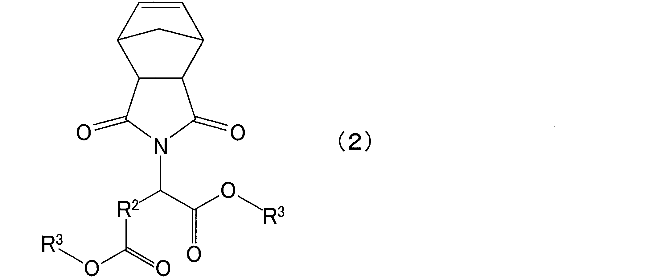
エポキシ基含有アクリレート化合物の具体例としては、アクリル酸グリシジル、メタクリル酸グリシジル、α-エチルアクリル酸グリシジル、α-n-プロピルアクリル酸グリシジル、α-n-ブチルアクリル酸グリシジル、アクリル酸-3,4-エポキシブチル、メタクリル酸-3,4-エポキシブチル、アクリル酸-6,7-エポキシヘプチル、メタクリル酸-6,7-エポキシヘプチル、α-エチルアクリル酸-6,7-エポキシヘプチル、アクリル酸-3,4-エポキシシクロヘキシルメチル、メタクリル酸-3,4-エポキシシクロヘキシルメチル等が挙げられる。
オキセタン基含有アクリレート化合物の具体例としては、(メタ)アクリル酸(3-メチルオキセタン-3-イル)メチル、(メタ)アクリル酸(3-エチルオキセタン-3-イル)メチル、(メタ)アクリル酸(3-メチルオキセタン-3-イル)エチル、(メタ)アクリル酸(3-エチルオキセタン-3-イル)エチル、(メタ)アクリル酸(3-クロロメチルオキセタン-3-イル)メチル、(メタ)アクリル酸(オキセタン-2-イル)メチル、(メタ)アクリル酸(2-メチルオキセタン-2-イル)メチル、(メタ)アクリル酸(2-エチルオキセタン-2-イル)メチル、(1-メチル-1-オキセタニル-2-フェニル)-3-(メタ)アクリレート、(1-メチル-1-オキセタニル)-2-トリフロロメチル-3-(メタ)アクリレート、および(1-メチル-1-オキセタニル)-4-トリフロロメチル-2-(メタ)アクリレート等が挙げられる。これらのうち、(メタ)アクリル酸、無水マレイン酸、(メタ)アクリル酸グリシジル、メタクリル酸-6,7-エポキシヘプチル等が好ましい。 Specific examples of the carboxylic acid having an acrylic group include (meth) acrylic acid [meaning acrylic acid and / or methacrylic acid. The same applies to methyl (meth) acrylate. ], Crotonic acid, maleic acid, fumaric acid, citraconic acid, mesaconic acid, glutaconic acid, phthalic acid mono- (2-((meth) acryloyloxy) ethyl), N- (carboxyphenyl) maleimide, N- (carboxyphenyl) ) (Meth) acrylamide and the like. Specific examples of the carboxylic acid anhydride having an acrylic group include maleic anhydride and citraconic anhydride.
Specific examples of the epoxy group-containing acrylate compound include glycidyl acrylate, glycidyl methacrylate, glycidyl α-ethyl acrylate, glycidyl α-n-propyl acrylate, glycidyl α-n-butyl acrylate,
Specific examples of the oxetane group-containing acrylate compound include (meth) acrylic acid (3-methyloxetane-3-yl) methyl, (meth) acrylic acid (3-ethyloxetane-3-yl) methyl, and (meth) acrylic acid. (3-methyloxetane-3-yl) ethyl, (meth) acrylic acid (3-ethyloxetane-3-yl) ethyl, (meth) acrylic acid (3-chloromethyloxetane-3-yl) methyl, (meth) Acrylic acid (oxetane-2-yl) methyl, (meth) acrylic acid (2-methyloxetane-2-yl) methyl, (meth) acrylic acid (2-ethyloxetane-2-yl) methyl, (1-methyl- 1-oxetanyl-2-phenyl) -3- (meth) acrylate, (1-methyl-1-oxetanyl) -2-trifluoromethyl-3- (me ) Acrylate, and (1-methyl-1-oxetanyl) -4-trifluoromethyl-2- (meth) acrylate. Of these, (meth) acrylic acid, maleic anhydride, glycidyl (meth) acrylate, methacrylic acid-6,7-epoxyheptyl and the like are preferable.
環状構造を構成している4級炭素原子に二つの環状構造が結合した骨格構造の具体例としては、フルオレン骨格、ビスフェノールフルオレン骨格、ビスアミノフェニルフルオレン骨格、エポキシ基を有するフルオレン骨格、アクリル基を有するフルオレン骨格等が挙げられる。
本発明で用いるカルド樹脂は、このカルド構造を有する骨格がそれに結合している官能基間の反応等により重合して形成される。カルド樹脂は、主鎖と嵩高い側鎖が一つの元素で繋がれた構造(カルド構造)をもち、主鎖に対してほぼ垂直方向に環状構造を有している。 The cardo resin used in the present invention is a resin having a cardo structure, that is, a skeleton structure in which two cyclic structures are bonded to a quaternary carbon atom constituting the cyclic structure. A common cardo structure is a fluorene ring bonded to a benzene ring.
Specific examples of the skeleton structure in which two cyclic structures are bonded to a quaternary carbon atom constituting the cyclic structure include a fluorene skeleton, a bisphenol fluorene skeleton, a bisaminophenyl fluorene skeleton, a fluorene skeleton having an epoxy group, and an acrylic group. And a fluorene skeleton having the same.
The cardo resin used in the present invention is formed by polymerizing a skeleton having the cardo structure by a reaction between functional groups bonded thereto. The cardo resin has a structure in which a main chain and bulky side chains are connected by one element (cardo structure), and has a ring structure in a direction substantially perpendicular to the main chain.

カルド樹脂は、カルド構造を有する単量体を重合して得られる重合体であるが、その他の共重合可能な単量体との共重合体であってもよい。
上記単量体の重合方法は、常法に従えばよく、たとえば、開環重合法や付加重合法等が採用される。 Monomers having a cardo structure include, for example, bis (glycidyloxyphenyl) fluorene type epoxy resin; condensate of bisphenolfluorene type epoxy resin and acrylic acid; 9,9-bis (4-hydroxyphenyl) fluorene, 9, Cardio structure-containing bisphenols such as 9-bis (4-hydroxy-3-methylphenyl) fluorene; 9,9-bis (cyanoalkyl) fluorenes such as 9,9-bis (cyanomethyl) fluorene; -9,9-bis (aminoalkyl) fluorenes such as bis (3-aminopropyl) fluorene;
The cardo resin is a polymer obtained by polymerizing a monomer having a cardo structure, but may be a copolymer with other copolymerizable monomers.
The polymerization method of the monomer may be according to a conventional method, and for example, a ring-opening polymerization method or an addition polymerization method is employed.
(R4)m-Si-(OR5)4-m (4) Although it does not specifically limit as polysiloxane resin used by this invention, Preferably the polymer obtained by mixing and making 1 type (s) or 2 types or more of organosilane represented by following formula (4) mentioned is mentioned.
(R 4 ) m -Si- (OR 5 ) 4-m (4)
これらの中でも、1,2-ナフトキノンジアジド-5-スルホン酸クロライドとフェノール性水酸基を有する化合物との縮合物が好ましく、1,1,3-トリス(2,5-ジメチル-4-ヒドロキシフェニル)-3-フェニルプロパン(1モル)と1,2-ナフトキノンジアジド-5-スルホン酸クロライド(1.9モル)との縮合物がより好ましい。 As the quinonediazide compound, for example, an ester compound of a quinonediazidesulfonic acid halide and a compound having a phenolic hydroxyl group can be used. Specific examples of the quinone diazide sulfonic acid halide include 1,2-naphthoquinone diazide-5-sulfonic acid chloride, 1,2-naphthoquinone diazide-4-sulfonic acid chloride, 1,2-benzoquinone diazide-5-sulfonic acid chloride, and the like. Can be mentioned. Representative examples of the compound having a phenolic hydroxyl group include 1,1,3-tris (2,5-dimethyl-4-hydroxyphenyl) -3-phenylpropane, 4,4 ′-[1- [4- [1 -[4-hydroxyphenyl] -1-methylethyl] phenyl] ethylidene] bisphenol and the like. Other compounds having a phenolic hydroxyl group include 2,3,4-trihydroxybenzophenone, 2,3,4,4′-tetrahydroxybenzophenone, 2-bis (4-hydroxyphenyl) propane, tris (4- Hydroxyphenyl) methane, 1,1,1-tris (4-hydroxy-3-methylphenyl) ethane, 1,1,2,2-tetrakis (4-hydroxyphenyl) ethane, novolak resin oligomer, phenolic hydroxyl group Examples thereof include oligomers obtained by copolymerizing one or more compounds and dicyclopentadiene.
Among these, a condensate of 1,2-naphthoquinonediazide-5-sulfonic acid chloride and a compound having a phenolic hydroxyl group is preferable, and 1,1,3-tris (2,5-dimethyl-4-hydroxyphenyl)- A condensate of 3-phenylpropane (1 mol) and 1,2-naphthoquinonediazide-5-sulfonic acid chloride (1.9 mol) is more preferred.
テトラメトキシシラン、テトラエトキシシラン、テトラ-n-プロポキシシラン、テトラ-i-プロポキシシラン、テトラ-n-ブトキシシランなどのテトラアルコキシシラン類、
メチルトリメトキシシラン、メチルトリエトキシシラン、エチルトリメトキシシラン、エチルトリエトキシシラン、n-プロピルトリメトキシシラン、n-プロピルトリエトキシシラン、i-プロピルトリメトキシシラン、i-プロピルトリエトキシシラン、n-ブチルトリメトキシシラン、n-ブチルトリエトキシシラン、n-ペンチルトリメトキシシラン、n-ヘキシルトリメトキシシラン、n-ヘプチルトリメトキシシラン、n-オクチルトリメトキシシラン、n-デシルトリメトキシシラン、p-スチリルトリメトキシシラン、ビニルトリメトキシシラン、ビニルトリエトキシシラン、シクロヘキシルトリメトキシシラン、シクロヘキシルトリメトキシシラン、シクロヘキシルトリエトキシシラン、フェニルトリメトキシシラン、フェニルトリエトキシシラン、3-クロロプロピルトリメトキシシラン、3-クロロプロピルトリエトキシシラン、3,3,3-トリフルオロプロピルトリメトキシシラン、3,3,3-トリフルオロプロピルトリエトキシシラン、3-アミノプロピルトリメトキシシラン、3-アミノプロピルトリエトキシシラン、N-2-(アミノエチル)-3-アミノプロピルトリメトキシシラン、N-フェニル-3-アミノプロピルトリメトキシシラン、2-ヒドロキシエチルトリメトキシシラン、2-ヒドロキシエチルトリエトキシシラン、2-ヒドロキシプロピルトリメトキシシラン、2-ヒドロキシプロピルトリエトキシシラン、3-ヒドロキシプロピルトリメトキシシラン、3-ヒドロキシプロピルトリエトキシシラン、3-メルカプトプロピルトリメトキシシラン、3-メルカプトプロピルトリエトキシシラン、3-イソシアナートプロピルトリメトキシシラン、3-イソシアナートプロピルトリエトキシシラン、3-グリシドキシプロピルトリメトキシシラン、3-グリシドキシプロピルトリエトキシシラン、2-(3,4-エポキシシクロヘキシル)エチルトリメトキシシラン、2-(3,4-エポキシシクロヘキシル)エチルトリエトキシシラン、3-(メタ)アクリルオキシプロピルトリメトキシシラン、3-(メタ)アクリルオキシプロピルトリエトキシシラン、3-ウレイドプロピルトリメトキシシラン、3-ウレイドプロピルトリエトキシシラン、3-エチル(トリメトキシシリルプロポキシメチル)オキセタン、3-エチル(トリエトキシシリルプロポキシメチル)オキセタン、3-トリエトキシシリル-N-(1,3-ジメチル-ブチリデン)プロピルアミン、ビス(トリエトキシシリルプロピル)テトラスルフィドなどのトリアルコキシシラン類、
ジメチルジメトキシシラン、ジメチルジエトキシシラン、ジエチルジメトキシシラン、ジエチルジエトキシシラン、ジ-n-プロピルジメトキシシラン、ジ-n-プロピルジエトキシシラン、ジ-i-プロピルジメトキシシラン、ジ-i-プロピルジエトキシシラン、ジ-n-ブチルジメトキシシラン、ジ-n-ペンチルジメトキシシラン、ジ-n-ペンチルジエトキシシラン、ジ-n-ヘキシルジメトキシシラン、ジ-n-ヘキシルジエトキシシラン、ジ-n-へプチルジメトキシシラン、ジ-n-ヘプチルジエトキシシラン、ジ-n-オクチルジメトキシシラン、ジ-n-オクチルジエトキシシラン、ジ-n-シクロヘキシルジメトキシシラン、ジ-n-シクロヘキシルジエトキシシラン、ジフェニルジメトキシシラン、ジフェニルジエトキシシラン、3-グリシドキシプロピルメチルジエトキシシラン、3-メタクリルオキシプロピルメチルジメトキシシラン、3-アクリルオキシプロピルメチルジメトキシシラン、3-メタクリルオキシプロピルメチルジエトキシシラン、3-アクリルオキシプロピルメチルジエトキシシラン、N-2-(アミノエチル)-3-アミノプロピルメチルジメトキシシランなどのジアルコキシシラン類の他、
メチルトリアセチルオキシシラン、ジメチルジアセチルオキシシラン等のケイ素原子含有化合物; As a coupling agent or a derivative thereof, for example,
Tetraalkoxysilanes such as tetramethoxysilane, tetraethoxysilane, tetra-n-propoxysilane, tetra-i-propoxysilane, tetra-n-butoxysilane,
Methyltrimethoxysilane, methyltriethoxysilane, ethyltrimethoxysilane, ethyltriethoxysilane, n-propyltrimethoxysilane, n-propyltriethoxysilane, i-propyltrimethoxysilane, i-propyltriethoxysilane, n- Butyltrimethoxysilane, n-butyltriethoxysilane, n-pentyltrimethoxysilane, n-hexyltrimethoxysilane, n-heptyltrimethoxysilane, n-octyltrimethoxysilane, n-decyltrimethoxysilane, p-styryl Trimethoxysilane, vinyltrimethoxysilane, vinyltriethoxysilane, cyclohexyltrimethoxysilane, cyclohexyltrimethoxysilane, cyclohexyltriethoxysilane, phenyltrimethoxysilane, phenyl Nyltriethoxysilane, 3-chloropropyltrimethoxysilane, 3-chloropropyltriethoxysilane, 3,3,3-trifluoropropyltrimethoxysilane, 3,3,3-trifluoropropyltriethoxysilane, 3-amino Propyltrimethoxysilane, 3-aminopropyltriethoxysilane, N-2- (aminoethyl) -3-aminopropyltrimethoxysilane, N-phenyl-3-aminopropyltrimethoxysilane, 2-hydroxyethyltrimethoxysilane, 2-hydroxyethyltriethoxysilane, 2-hydroxypropyltrimethoxysilane, 2-hydroxypropyltriethoxysilane, 3-hydroxypropyltrimethoxysilane, 3-hydroxypropyltriethoxysilane, 3-mercaptopropyl Limethoxysilane, 3-mercaptopropyltriethoxysilane, 3-isocyanatopropyltrimethoxysilane, 3-isocyanatopropyltriethoxysilane, 3-glycidoxypropyltrimethoxysilane, 3-glycidoxypropyltriethoxysilane, 2- (3,4-epoxycyclohexyl) ethyltrimethoxysilane, 2- (3,4-epoxycyclohexyl) ethyltriethoxysilane, 3- (meth) acryloxypropyltrimethoxysilane, 3- (meth) acryloxypropyl Triethoxysilane, 3-ureidopropyltrimethoxysilane, 3-ureidopropyltriethoxysilane, 3-ethyl (trimethoxysilylpropoxymethyl) oxetane, 3-ethyl (triethoxysilylpropoxymethyl) Kisetan, 3-triethoxysilyl-N-(1,3-dimethyl - butylidene) propylamine, trialkoxysilanes such as bis (triethoxysilylpropyl) tetrasulfide,
Dimethyldimethoxysilane, dimethyldiethoxysilane, diethyldimethoxysilane, diethyldiethoxysilane, di-n-propyldimethoxysilane, di-n-propyldiethoxysilane, di-i-propyldimethoxysilane, di-i-propyldiethoxy Silane, di-n-butyldimethoxysilane, di-n-pentyldimethoxysilane, di-n-pentyldiethoxysilane, di-n-hexyldimethoxysilane, di-n-hexyldiethoxysilane, di-n-heptyl Dimethoxysilane, di-n-heptyldiethoxysilane, di-n-octyldimethoxysilane, di-n-octyldiethoxysilane, di-n-cyclohexyldimethoxysilane, di-n-cyclohexyldiethoxysilane, diphenyldimethoxysilane, Diphenyldie Xysilane, 3-glycidoxypropylmethyldiethoxysilane, 3-methacryloxypropylmethyldimethoxysilane, 3-acryloxypropylmethyldimethoxysilane, 3-methacryloxypropylmethyldiethoxysilane, 3-acryloxypropylmethyldiethoxysilane In addition to dialkoxysilanes such as N-2- (aminoethyl) -3-aminopropylmethyldimethoxysilane,
Silicon atom-containing compounds such as methyltriacetyloxysilane and dimethyldiacetyloxysilane;
アセトアルコキシアルミウムジイソプロピレート等のアルミニウム原子含有化合物;
テトラノルマルプロポキシジルコニウム、テトラノルマルブトキシジルコニウム、ジルコニウムテトラアセチルアセトネート、ジルコニウムトリブトキシアセチルアセトネート、ジルコニウムモノブトキシアセチルアセトネートビス(エチルアセトアセテート)、ジルコニウムジブトキシビス(エチルアセトアセテート)、ジルコニウムテトラアセチルアセトネート、ジルコニウムトリブトキシステアレート等のジルコニウム原子含有化合物;が挙げられる。 Tetra-i-propoxytitanium, tetra-n-butoxytitanium, tetrakis (2-ethylhexyloxy) titanium, titanium-i-propoxyoctylene glycolate, di-i-propoxybis (acetylacetonato) titanium, propanedioxy Titanium bis (ethyl acetoacetate), tri-n-butoxy titanium monostearate, di-i-propoxy titanium distearate, titanium stearate, di-i-propoxy titanium diisostearate, (2-n-butoxycarbonylbenzoyl) In addition to oxy) tributoxytitanium, di-n-butoxybis (triethanolaminato) titanium, and the preneact series (manufactured by Ajinomoto Fine Techno Co., Ltd.)
Aluminum atom-containing compounds such as acetoalkoxyaluminum diisopropylate;
Tetranormal propoxyzirconium, tetranormalbutoxyzirconium, zirconium tetraacetylacetonate, zirconium tributoxyacetylacetonate, zirconium monobutoxyacetylacetonate bis (ethylacetoacetate), zirconium dibutoxybis (ethylacetoacetate), zirconium tetraacetylacetate And zirconium atom-containing compounds such as zirconium tributoxy systemate.
潜像パターンを有するパッシベーション膜7に現像液を接触させる方法としては、たとえば、パドル法、スプレー法、ディッピング法等の方法が用いられる。現像は、通常、0~100℃、好ましくは5~55℃、より好ましくは10~30℃の範囲で、通常、30~180秒間の範囲とされる。 As an aqueous medium of the alkaline aqueous solution, water; a water-soluble organic solvent such as methanol or ethanol can be used. The alkaline aqueous solution may have a surfactant added in an appropriate amount.
As a method of bringing the developer into contact with the
なお、各特性の定義および評価方法は、以下のとおりである。 Hereinafter, the present invention will be described more specifically with reference to examples and comparative examples. “Part” and “%” in each example are based on weight unless otherwise specified.
In addition, the definition and evaluation method of each characteristic are as follows.
得られた薄膜トランジスタについて、大気下・暗室中にて半導体パラメータアナライザー(Agilent社製、4156C)を用いて、ゲート電圧を-60Vから+20Vまで変化させることによって、ゲート電圧の変化に対するソース・ドレイン間に流れる電流の変化を測定した。そして、測定の結果、ソース・ドレイン間に流れる電流の値が、Id=100nA×(W/L)(ただし、Wはチャネル幅、Lはチャネル長、Idはドレイン電流)となった時の電圧を、閾値電圧Vthとした。図4に、実施例1および比較例2で得られた薄膜トランジスタの、ゲート電圧の変化に対するソース・ドレイン間に流れる電流の変化を示す。 <Threshold voltage Vth>
With respect to the obtained thin film transistor, by changing the gate voltage from −60 V to +20 V using a semiconductor parameter analyzer (Agilent, 4156C) in the atmosphere and in the dark room, the source and the drain with respect to the change of the gate voltage are changed. The change in flowing current was measured. As a result of measurement, the voltage when the value of the current flowing between the source and the drain becomes Id = 100 nA × (W / L) (W is the channel width, L is the channel length, and Id is the drain current) Is defined as a threshold voltage Vth. FIG. 4 shows changes in the current flowing between the source and the drain with respect to changes in the gate voltage of the thin film transistors obtained in Example 1 and Comparative Example 2.
得られた薄膜トランジスタについて、大気下・暗室中にて半導体パラメータアナライザー(Agilent社製、4156C)を用いて、ゲート電圧を-60Vから+20Vまで変化させることによって、ゲート電圧の変化に対するソース・ドレイン間に流れる電流の変化を測定し、薄膜トランジスタの飽和領域から電界効果移動度を、下記式にしたがって求めた。
Id=μCin・W・(Vg-Vth)2/2L
(ただし、Cinはゲート絶縁膜の単位面積あたりの静電容量、Wはチャネル幅、Lはチャネル長、Vgはゲート電圧、Idはドレイン電流、μは移動度、Vthはゲートの閾値電圧である。) <Mobility>
With respect to the obtained thin film transistor, by changing the gate voltage from −60 V to +20 V using a semiconductor parameter analyzer (Agilent, 4156C) in the atmosphere and in the dark room, the source and the drain with respect to the change of the gate voltage are changed. The change in the flowing current was measured, and the field effect mobility was determined from the saturation region of the thin film transistor according to the following formula.
Id = μCin · W · (Vg−Vth) 2 / 2L
(Where Cin is the capacitance per unit area of the gate insulating film, W is the channel width, L is the channel length, Vg is the gate voltage, Id is the drain current, μ is the mobility, and Vth is the gate threshold voltage. .)
<環状オレフィン重合体(A-1)の調製>
N-フェニル-ビシクロ[2.2.1]ヘプト-5-エン-2,3-ジカルボキシイミド(NBPI)40モル%、および4-ヒドロキシカルボニルテトラシクロ[6.2.1.13,6.02,7]ドデカ-9-エン(TCDC)60モル%からなる単量体混合物100部、1,5-ヘキサジエン2.0部、(1,3-ジメシチルイミダゾリン-2-イリデン)(トリシクロヘキシルホスフィン)ベンジリデンルテニウムジクロリド(「Org.Lett.,第1巻,953頁,1999年」に記載された方法で合成した)0.02部、およびジエチレングリコールエチルメチルエーテル200部を、窒素置換したガラス製耐圧反応器に仕込み、攪拌しつつ80℃にて4時間反応させて重合反応液を得た。 << Synthesis Example 1 >>
<Preparation of Cyclic Olefin Polymer (A-1)>
40 mol% N-phenyl-bicyclo [2.2.1] hept-5-ene-2,3-dicarboximide (NBPI), and 4-hydroxycarbonyltetracyclo [6.2.1.1 3,6 . 0 2,7 ] dodeca-9-ene (TCDC) 100 parts monomer mixture, 1,5-hexadiene 2.0 parts, (1,3-dimesitylimidazoline-2-ylidene) ( 0.02 part of tricyclohexylphosphine) benzylidene ruthenium dichloride (synthesized by the method described in “Org. Lett., Vol. 1, page 953, 1999”) and 200 parts of diethylene glycol ethyl methyl ether were substituted with nitrogen. The polymerization reaction liquid was obtained by charging into a glass pressure-resistant reactor and reacting at 80 ° C. for 4 hours while stirring.
<樹脂組成物の調製>
樹脂(A)として、合成例1で得られた環状オレフィン重合体(A-1)の重合体溶液291部(環状オレフィン重合体(A-1)として100部)、アルコキシシリル基含有(メタ)アクリレート化合物(B)として、3-アクリロキシプロピルトリメトキシシラン(製品名「KBM-5103」、信越化学工業社製)1部、4官能以上の(メタ)アクリレート化合物(C)として、ジペンタエリスリトールペンタ/ヘキサアクリレート(製品名「アロニックスM-406 ペンタ25-35%」、東亜合成社製)3部、光重合開始剤(D)として、2-ヒドロキシ-1-{4-[4-(2-ヒドロキシ-2-メチル-プロピオニル)-ベンジル]フェニル}-2-メチル-プロパン-1-オン(製品名「Irgacure127」、BASF社製)1部、架橋剤(E)として、エポキシ化ブタンテトラカルボン酸テトラキス(3-シクロヘキセニルメチル)修飾ε-カプロラクトン(脂肪族環状4官能性のエポキシ樹脂、製品名「エポリードGT401」、ダイセル化学工業社製)15部、シリコーン系界面活性剤(製品名「KP-341」、信越化学工業社製)0.03部、および、溶剤として、エチレングリコールエチルメチルエーテル270部を混合し、溶解させた後、孔径0.45μmのポリテトラフルオロエチレン製フィルターでろ過して、樹脂組成物を調製した。 Example 1
<Preparation of resin composition>
As resin (A), 291 parts of polymer solution of cyclic olefin polymer (A-1) obtained in Synthesis Example 1 (100 parts as cyclic olefin polymer (A-1)), alkoxysilyl group-containing (meth) As acrylate compound (B), 1 part of 3-acryloxypropyltrimethoxysilane (product name “KBM-5103”, manufactured by Shin-Etsu Chemical Co., Ltd.), dipentaerythritol as (meth) acrylate compound (C) having 4 or more functional groups 3 parts of penta / hexaacrylate (product name “Aronix M-406 Penta 25-35%”, manufactured by Toa Gosei Co., Ltd.), as photopolymerization initiator (D), 2-hydroxy-1- {4- [4- (2 -Hydroxy-2-methyl-propionyl) -benzyl] phenyl} -2-methyl-propan-1-one (product name “Irgacure 127”, BAS F part), 1 part, epoxidized butanetetracarboxylic acid tetrakis (3-cyclohexenylmethyl) modified ε-caprolactone (aliphatic cyclic tetrafunctional epoxy resin, product name “Epolide GT401”) as a crosslinking agent (E), Daicel Chemical Industries, Ltd.) 15 parts, silicone surfactant (product name “KP-341”, Shin-Etsu Chemical Co., Ltd.) 0.03 parts, and ethylene glycol ethyl methyl ether 270 parts as a solvent, After dissolution, the mixture was filtered through a polytetrafluoroethylene filter having a pore diameter of 0.45 μm to prepare a resin composition.
次いで、以下の方法により、図1に示す構成を有する薄膜トランジスタを作製した。すなわち、まず、基板2としてのp型シリコン基板を準備し、p型シリコン基板について、酸素と水素の雰囲気下、1000℃、13分の条件で熱処理を行うことで、p型シリコン基板上に、ゲート絶縁膜となる100nmの熱酸化膜を形成した。次いで、その上に50nmのIn-Ga-Zn-O系非単結晶膜を、成膜時のAr/O2の流量比を50%としたスパッタリング法により、形成した。次いで、In-Ga-Zn-O系非単結晶膜をパターニングするため、エッチングのマスク用のポジ型フォトレジストをスピンコート法により半導体層上に塗布し、ホットプレートを用いて溶媒を除去することでレジスト膜を形成し、これに続いて、露光工程、現像工程を経てレジスト膜をパターニングした。次いで、形成したマスクを使用して、燐酸によるウェットエッチングにより、In-Ga-Zn-O系非単結晶膜をアイランド状にパターニングし、これに続いて、剥離液を用いてレジスト膜を除去することで、半導体層4を形成した(図2(A)参照)。次いで、水蒸気雰囲気下(H2O/O2:10%H2O)で、220℃、1時間の条件で加熱処理を行った。 <Production of Thin Film Transistor>
Next, a thin film transistor having the configuration shown in FIG. 1 was produced by the following method. That is, first, a p-type silicon substrate as a
樹脂膜の焼成を行った後の冷却を、N2雰囲気下、0.5℃/分の冷却速度にて、150℃まで冷却を行った以外は、実施例1と同様にして、薄膜トランジスタを得て、同様に評価を行った。結果を表1に示す。 Example 2
A thin film transistor was obtained in the same manner as in Example 1 except that the resin film was cooled to 150 ° C. in a N 2 atmosphere at a cooling rate of 0.5 ° C./min. The same evaluation was performed. The results are shown in Table 1.
樹脂膜の焼成を行った後の冷却を、N2雰囲気下、5℃/分の冷却速度にて、150℃まで冷却を行った以外は、実施例1と同様にして、薄膜トランジスタを得て、同様に評価を行った。結果を表1に示す。 Example 3
A thin film transistor was obtained in the same manner as in Example 1 except that cooling after firing the resin film was performed at 150 ° C. under a N 2 atmosphere at a cooling rate of 5 ° C./min. Evaluation was performed in the same manner. The results are shown in Table 1.
樹脂膜の焼成を行った後、即座に、焼成後の樹脂膜形成基板を、大気雰囲気、室温の条件下に取り出した以外は、実施例1と同様にして、薄膜トランジスタを得て、同様に評価を行った。結果を表1に示す。 << Comparative Example 1 >>
Immediately after firing the resin film, a thin film transistor was obtained and evaluated in the same manner as in Example 1 except that the fired resin film-formed substrate was taken out under atmospheric conditions and room temperature. Went. The results are shown in Table 1.
パッシベーション膜7を形成しなかった以外は、実施例1と同様にして、薄膜トランジスタを得て、同様に評価を行った。すなわち、比較例2においては、樹脂組成物を用いた樹脂膜の形成を行わずに、実施例1と同様の条件で焼成および冷却を行うことで、薄膜トランジスタを得た。すなわち、比較例2においては、パッシベーション膜の形成条件ではなく、パッシベーション膜無しでの加熱冷却の条件を示す。結果を表1に示す。 << Comparative Example 2 >>
A thin film transistor was obtained and evaluated in the same manner as in Example 1 except that the

一方、樹脂膜の焼成を行った後、0.5~5℃/分の冷却速度で冷却を行わなかった場合、および、パッシベーション膜を形成しなかった場合には、得られる薄膜トランジスタは、いずれも、閾値電圧Vthの絶対値が大きくなり、しかも、移動度も低いものであった(比較例1,2)。 As shown in Table 1, when the cooling rate at the time of cooling after firing the resin film is in the range of 0.5 to 5 ° C./min, any of the obtained thin film transistors has a threshold value. The voltage Vth was close to zero and had high mobility (Examples 1 to 3).
On the other hand, after the baking of the resin film, when the cooling is not performed at a cooling rate of 0.5 to 5 ° C./min, and when the passivation film is not formed, any of the obtained thin film transistors The absolute value of the threshold voltage Vth is large and the mobility is low (Comparative Examples 1 and 2).
2…基板
3…ゲート電極
4…半導体層
5…ソース電極
6…ドレイン電極
7…パッシベーション膜 DESCRIPTION OF SYMBOLS 1 ...
Claims (8)
- 基板上に、無機酸化物半導体を含む半導体層を形成する半導体層形成工程と、
前記半導体層を覆うように、有機材料からなるパッシベーション膜を成膜するパッシベーション膜形成工程と、
前記パッシベーション膜を焼成する焼成工程と、
焼成後、冷却する冷却工程とを備える半導体素子の製造方法であって、
前記冷却工程における冷却を行う際における、前記焼成工程の焼成時の焼成温度から、焼成時の焼成温度より50℃低い温度までの冷却速度を、0.5~5℃/分の範囲で実質的に制御することを特徴とする半導体素子の製造方法。 A semiconductor layer forming step of forming a semiconductor layer containing an inorganic oxide semiconductor on the substrate;
A passivation film forming step of forming a passivation film made of an organic material so as to cover the semiconductor layer;
A firing step of firing the passivation film;
A method for producing a semiconductor element comprising a cooling step for cooling after firing,
When performing the cooling in the cooling step, the cooling rate from the firing temperature at the firing step in the firing step to a temperature lower by 50 ° C. than the firing temperature at the firing step is substantially within a range of 0.5 to 5 ° C./min. A method of manufacturing a semiconductor element, characterized by controlling - 前記焼成工程の焼成温度が、200~300℃であることを特徴とする請求項1に記載の半導体素子の製造方法。 2. The method of manufacturing a semiconductor element according to claim 1, wherein a baking temperature in the baking step is 200 to 300 ° C.
- 前記冷却工程における冷却を行う際における、前記焼成工程の焼成温度から、150℃までの冷却速度を、0.5~5℃/分の範囲で実質的に制御することを特徴とする請求項1または2に記載の半導体素子の製造方法。 2. The cooling rate from the firing temperature in the firing step to 150 ° C. during the cooling in the cooling step is substantially controlled in a range of 0.5 to 5 ° C./min. Or the manufacturing method of the semiconductor element of 2.
- 前記焼成工程の焼成および前記冷却工程における冷却を、非酸化性雰囲気下で行うことを特徴とする請求項1~3のいずれかに記載の半導体素子の製造方法。 The method for manufacturing a semiconductor element according to any one of claims 1 to 3, wherein the firing in the firing step and the cooling in the cooling step are performed in a non-oxidizing atmosphere.
- 前記パッシベーション膜を、環状オレフィン樹脂、アクリル樹脂、カルド樹脂、ポリシロキサン樹脂およびポリイミド樹脂からなる群から選ばれる少なくとも1種の樹脂を含む樹脂組成物を用いて形成することを特徴とする請求項1~4のいずれかに記載の半導体素子の製造方法。 The said passivation film is formed using the resin composition containing at least 1 sort (s) of resin chosen from the group which consists of cyclic olefin resin, acrylic resin, cardo resin, polysiloxane resin, and polyimide resin. 5. A method for producing a semiconductor device according to any one of items 1 to 4.
- 前記パッシベーション膜を、プロトン性極性基を有する環状オレフィン樹脂を含む樹脂組成物を用いて形成することを特徴とする請求項5に記載の半導体素子の製造方法。 The method for manufacturing a semiconductor element according to claim 5, wherein the passivation film is formed using a resin composition containing a cyclic olefin resin having a protic polar group.
- 前記樹脂組成物が、アルコキシシリル基含有(メタ)アクリレート化合物、4官能以上の(メタ)アクリレート化合物、光重合開始剤、および架橋剤をさらに含有する請求項6に記載の半導体素子の製造方法。 The method for producing a semiconductor element according to claim 6, wherein the resin composition further contains an alkoxysilyl group-containing (meth) acrylate compound, a tetrafunctional or higher-functional (meth) acrylate compound, a photopolymerization initiator, and a crosslinking agent.
- 請求項1~7のいずれかに記載の方法により得られる半導体素子。 A semiconductor element obtained by the method according to any one of claims 1 to 7.
Priority Applications (4)
| Application Number | Priority Date | Filing Date | Title |
|---|---|---|---|
| KR1020167013682A KR102269609B1 (en) | 2013-11-28 | 2014-11-25 | Semiconductor element manufacturing method |
| CN201480063979.5A CN105993065B (en) | 2013-11-28 | 2014-11-25 | The manufacturing method of semiconductor element |
| JP2015550917A JP6509740B2 (en) | 2013-11-28 | 2014-11-25 | Semiconductor device manufacturing method |
| US15/039,335 US10446690B2 (en) | 2013-11-28 | 2014-11-25 | Method of production of semiconductor device |
Applications Claiming Priority (2)
| Application Number | Priority Date | Filing Date | Title |
|---|---|---|---|
| JP2013246261 | 2013-11-28 | ||
| JP2013-246261 | 2013-11-28 |
Publications (1)
| Publication Number | Publication Date |
|---|---|
| WO2015080071A1 true WO2015080071A1 (en) | 2015-06-04 |
Family
ID=53199011
Family Applications (1)
| Application Number | Title | Priority Date | Filing Date |
|---|---|---|---|
| PCT/JP2014/081027 WO2015080071A1 (en) | 2013-11-28 | 2014-11-25 | Semiconductor element manufacturing method |
Country Status (6)
| Country | Link |
|---|---|
| US (1) | US10446690B2 (en) |
| JP (1) | JP6509740B2 (en) |
| KR (1) | KR102269609B1 (en) |
| CN (1) | CN105993065B (en) |
| TW (1) | TWI652369B (en) |
| WO (1) | WO2015080071A1 (en) |
Cited By (2)
| Publication number | Priority date | Publication date | Assignee | Title |
|---|---|---|---|---|
| US20190022978A1 (en) * | 2016-01-08 | 2019-01-24 | Dongwoo Fine-Chem Co., Ltd. | Film touch sensor and method for fabricating the same |
| US20190022977A1 (en) * | 2016-01-08 | 2019-01-24 | Dongwoo Fine-Chem Co., Ltd. | Film touch sensor and method for fabricating the same |
Families Citing this family (3)
| Publication number | Priority date | Publication date | Assignee | Title |
|---|---|---|---|---|
| US9728500B2 (en) * | 2015-12-17 | 2017-08-08 | Intel Corporation | Integrated circuit surface layer with adhesion-functional group |
| CN110741427B (en) * | 2017-11-10 | 2021-10-22 | 深圳市柔宇科技股份有限公司 | Manufacturing method of flexible panel, flexible panel and display device |
| KR102431923B1 (en) * | 2020-11-30 | 2022-08-11 | 김성진 | Method for manufacturing thin film transistor |
Citations (3)
| Publication number | Priority date | Publication date | Assignee | Title |
|---|---|---|---|---|
| JP2010199390A (en) * | 2009-02-26 | 2010-09-09 | Nippon Zeon Co Ltd | Method of manufacturing thin film transistor, thin film transistor, and display device |
| JP2011077514A (en) * | 2009-09-04 | 2011-04-14 | Semiconductor Energy Lab Co Ltd | Method of manufacturing semiconductor device |
| WO2011108533A1 (en) * | 2010-03-04 | 2011-09-09 | 日本ゼオン株式会社 | Method for producing semiconductor element substrate |
Family Cites Families (2)
| Publication number | Priority date | Publication date | Assignee | Title |
|---|---|---|---|---|
| JP4540201B2 (en) * | 2000-09-13 | 2010-09-08 | 独立行政法人産業技術総合研究所 | Method for manufacturing semiconductor device having ZnO-based oxide semiconductor layer |
| WO2012117439A1 (en) * | 2011-02-28 | 2012-09-07 | パナソニック株式会社 | Thin-film semiconductor device and manufacturing method therefor |
-
2014
- 2014-11-25 CN CN201480063979.5A patent/CN105993065B/en active Active
- 2014-11-25 WO PCT/JP2014/081027 patent/WO2015080071A1/en active Application Filing
- 2014-11-25 KR KR1020167013682A patent/KR102269609B1/en active IP Right Grant
- 2014-11-25 JP JP2015550917A patent/JP6509740B2/en active Active
- 2014-11-25 US US15/039,335 patent/US10446690B2/en active Active
- 2014-11-27 TW TW103141124A patent/TWI652369B/en active
Patent Citations (3)
| Publication number | Priority date | Publication date | Assignee | Title |
|---|---|---|---|---|
| JP2010199390A (en) * | 2009-02-26 | 2010-09-09 | Nippon Zeon Co Ltd | Method of manufacturing thin film transistor, thin film transistor, and display device |
| JP2011077514A (en) * | 2009-09-04 | 2011-04-14 | Semiconductor Energy Lab Co Ltd | Method of manufacturing semiconductor device |
| WO2011108533A1 (en) * | 2010-03-04 | 2011-09-09 | 日本ゼオン株式会社 | Method for producing semiconductor element substrate |
Cited By (4)
| Publication number | Priority date | Publication date | Assignee | Title |
|---|---|---|---|---|
| US20190022978A1 (en) * | 2016-01-08 | 2019-01-24 | Dongwoo Fine-Chem Co., Ltd. | Film touch sensor and method for fabricating the same |
| US20190022977A1 (en) * | 2016-01-08 | 2019-01-24 | Dongwoo Fine-Chem Co., Ltd. | Film touch sensor and method for fabricating the same |
| US10870260B2 (en) * | 2016-01-08 | 2020-12-22 | Dongwoo Fine-Chem Co., Ltd. | Film touch sensor and method for fabricating the same |
| US10894390B2 (en) * | 2016-01-08 | 2021-01-19 | Dongwoo Fine-Chem Co., Ltd. | Film touch sensor and method for fabricating the same |
Also Published As
| Publication number | Publication date |
|---|---|
| KR20160093610A (en) | 2016-08-08 |
| JPWO2015080071A1 (en) | 2017-03-16 |
| CN105993065A (en) | 2016-10-05 |
| KR102269609B1 (en) | 2021-06-24 |
| JP6509740B2 (en) | 2019-05-08 |
| TW201527577A (en) | 2015-07-16 |
| US10446690B2 (en) | 2019-10-15 |
| US20170186874A1 (en) | 2017-06-29 |
| CN105993065B (en) | 2019-03-08 |
| TWI652369B (en) | 2019-03-01 |
Similar Documents
| Publication | Publication Date | Title |
|---|---|---|
| JP5747908B2 (en) | Manufacturing method of semiconductor element substrate | |
| US10254648B2 (en) | Radiation-sensitive resin composition, resin film, and electronic device | |
| TWI662363B (en) | Radiation-sensitive resin composition and electronic component | |
| WO2012165448A1 (en) | Resin composition and semiconductor element substrate | |
| JP6509740B2 (en) | Semiconductor device manufacturing method | |
| WO2012133617A1 (en) | Resin composition and semiconductor element substrate | |
| JP6601394B2 (en) | Radiation-sensitive resin composition, resin film, and electronic component | |
| JP5589286B2 (en) | THIN FILM TRANSISTOR MANUFACTURING METHOD, THIN FILM TRANSISTOR AND DISPLAY DEVICE | |
| JP6248561B2 (en) | Radiation sensitive resin composition and laminate | |
| JP6485355B2 (en) | Resin composition, resin film, and electronic component | |
| JP2013130816A (en) | Resin composition for permanent film and electronic component | |
| JP5682413B2 (en) | Semiconductor device substrate | |
| JP6539464B2 (en) | Semiconductor device manufacturing method |
Legal Events
| Date | Code | Title | Description |
|---|---|---|---|
| 121 | Ep: the epo has been informed by wipo that ep was designated in this application |
Ref document number: 14866428 Country of ref document: EP Kind code of ref document: A1 |
|
| ENP | Entry into the national phase |
Ref document number: 2015550917 Country of ref document: JP Kind code of ref document: A |
|
| ENP | Entry into the national phase |
Ref document number: 20167013682 Country of ref document: KR Kind code of ref document: A |
|
| WWE | Wipo information: entry into national phase |
Ref document number: 15039335 Country of ref document: US |
|
| NENP | Non-entry into the national phase |
Ref country code: DE |
|
| 122 | Ep: pct application non-entry in european phase |
Ref document number: 14866428 Country of ref document: EP Kind code of ref document: A1 |