WO2015072213A1 - フィールドシーケンシャル液晶表示装置およびその駆動方法 - Google Patents
フィールドシーケンシャル液晶表示装置およびその駆動方法 Download PDFInfo
- Publication number
- WO2015072213A1 WO2015072213A1 PCT/JP2014/073284 JP2014073284W WO2015072213A1 WO 2015072213 A1 WO2015072213 A1 WO 2015072213A1 JP 2014073284 W JP2014073284 W JP 2014073284W WO 2015072213 A1 WO2015072213 A1 WO 2015072213A1
- Authority
- WO
- WIPO (PCT)
- Prior art keywords
- data
- field
- video data
- backlight
- liquid crystal
- Prior art date
- Legal status (The legal status is an assumption and is not a legal conclusion. Google has not performed a legal analysis and makes no representation as to the accuracy of the status listed.)
- Ceased
Links
Images









Classifications
-
- G—PHYSICS
- G09—EDUCATION; CRYPTOGRAPHY; DISPLAY; ADVERTISING; SEALS
- G09G—ARRANGEMENTS OR CIRCUITS FOR CONTROL OF INDICATING DEVICES USING STATIC MEANS TO PRESENT VARIABLE INFORMATION
- G09G3/00—Control arrangements or circuits, of interest only in connection with visual indicators other than cathode-ray tubes
- G09G3/20—Control arrangements or circuits, of interest only in connection with visual indicators other than cathode-ray tubes for presentation of an assembly of a number of characters, e.g. a page, by composing the assembly by combination of individual elements arranged in a matrix no fixed position being assigned to or needed to be assigned to the individual characters or partial characters
- G09G3/34—Control arrangements or circuits, of interest only in connection with visual indicators other than cathode-ray tubes for presentation of an assembly of a number of characters, e.g. a page, by composing the assembly by combination of individual elements arranged in a matrix no fixed position being assigned to or needed to be assigned to the individual characters or partial characters by control of light from an independent source
- G09G3/3406—Control of illumination source
- G09G3/3413—Details of control of colour illumination sources
-
- G—PHYSICS
- G09—EDUCATION; CRYPTOGRAPHY; DISPLAY; ADVERTISING; SEALS
- G09G—ARRANGEMENTS OR CIRCUITS FOR CONTROL OF INDICATING DEVICES USING STATIC MEANS TO PRESENT VARIABLE INFORMATION
- G09G3/00—Control arrangements or circuits, of interest only in connection with visual indicators other than cathode-ray tubes
- G09G3/20—Control arrangements or circuits, of interest only in connection with visual indicators other than cathode-ray tubes for presentation of an assembly of a number of characters, e.g. a page, by composing the assembly by combination of individual elements arranged in a matrix no fixed position being assigned to or needed to be assigned to the individual characters or partial characters
- G09G3/34—Control arrangements or circuits, of interest only in connection with visual indicators other than cathode-ray tubes for presentation of an assembly of a number of characters, e.g. a page, by composing the assembly by combination of individual elements arranged in a matrix no fixed position being assigned to or needed to be assigned to the individual characters or partial characters by control of light from an independent source
- G09G3/3406—Control of illumination source
- G09G3/342—Control of illumination source using several illumination sources separately controlled corresponding to different display panel areas, e.g. along one dimension such as lines
- G09G3/3426—Control of illumination source using several illumination sources separately controlled corresponding to different display panel areas, e.g. along one dimension such as lines the different display panel areas being distributed in two dimensions, e.g. matrix
-
- G—PHYSICS
- G09—EDUCATION; CRYPTOGRAPHY; DISPLAY; ADVERTISING; SEALS
- G09G—ARRANGEMENTS OR CIRCUITS FOR CONTROL OF INDICATING DEVICES USING STATIC MEANS TO PRESENT VARIABLE INFORMATION
- G09G3/00—Control arrangements or circuits, of interest only in connection with visual indicators other than cathode-ray tubes
- G09G3/20—Control arrangements or circuits, of interest only in connection with visual indicators other than cathode-ray tubes for presentation of an assembly of a number of characters, e.g. a page, by composing the assembly by combination of individual elements arranged in a matrix no fixed position being assigned to or needed to be assigned to the individual characters or partial characters
- G09G3/34—Control arrangements or circuits, of interest only in connection with visual indicators other than cathode-ray tubes for presentation of an assembly of a number of characters, e.g. a page, by composing the assembly by combination of individual elements arranged in a matrix no fixed position being assigned to or needed to be assigned to the individual characters or partial characters by control of light from an independent source
- G09G3/36—Control arrangements or circuits, of interest only in connection with visual indicators other than cathode-ray tubes for presentation of an assembly of a number of characters, e.g. a page, by composing the assembly by combination of individual elements arranged in a matrix no fixed position being assigned to or needed to be assigned to the individual characters or partial characters by control of light from an independent source using liquid crystals
- G09G3/3611—Control of matrices with row and column drivers
- G09G3/3674—Details of drivers for scan electrodes
-
- G—PHYSICS
- G09—EDUCATION; CRYPTOGRAPHY; DISPLAY; ADVERTISING; SEALS
- G09G—ARRANGEMENTS OR CIRCUITS FOR CONTROL OF INDICATING DEVICES USING STATIC MEANS TO PRESENT VARIABLE INFORMATION
- G09G3/00—Control arrangements or circuits, of interest only in connection with visual indicators other than cathode-ray tubes
- G09G3/20—Control arrangements or circuits, of interest only in connection with visual indicators other than cathode-ray tubes for presentation of an assembly of a number of characters, e.g. a page, by composing the assembly by combination of individual elements arranged in a matrix no fixed position being assigned to or needed to be assigned to the individual characters or partial characters
- G09G3/34—Control arrangements or circuits, of interest only in connection with visual indicators other than cathode-ray tubes for presentation of an assembly of a number of characters, e.g. a page, by composing the assembly by combination of individual elements arranged in a matrix no fixed position being assigned to or needed to be assigned to the individual characters or partial characters by control of light from an independent source
- G09G3/36—Control arrangements or circuits, of interest only in connection with visual indicators other than cathode-ray tubes for presentation of an assembly of a number of characters, e.g. a page, by composing the assembly by combination of individual elements arranged in a matrix no fixed position being assigned to or needed to be assigned to the individual characters or partial characters by control of light from an independent source using liquid crystals
- G09G3/3611—Control of matrices with row and column drivers
- G09G3/3685—Details of drivers for data electrodes
-
- G—PHYSICS
- G09—EDUCATION; CRYPTOGRAPHY; DISPLAY; ADVERTISING; SEALS
- G09G—ARRANGEMENTS OR CIRCUITS FOR CONTROL OF INDICATING DEVICES USING STATIC MEANS TO PRESENT VARIABLE INFORMATION
- G09G5/00—Control arrangements or circuits for visual indicators common to cathode-ray tube indicators and other visual indicators
- G09G5/02—Control arrangements or circuits for visual indicators common to cathode-ray tube indicators and other visual indicators characterised by the way in which colour is displayed
- G09G5/026—Control of mixing and/or overlay of colours in general
-
- G—PHYSICS
- G09—EDUCATION; CRYPTOGRAPHY; DISPLAY; ADVERTISING; SEALS
- G09G—ARRANGEMENTS OR CIRCUITS FOR CONTROL OF INDICATING DEVICES USING STATIC MEANS TO PRESENT VARIABLE INFORMATION
- G09G2300/00—Aspects of the constitution of display devices
- G09G2300/04—Structural and physical details of display devices
- G09G2300/0439—Pixel structures
- G09G2300/0452—Details of colour pixel setup, e.g. pixel composed of a red, a blue and two green components
-
- G—PHYSICS
- G09—EDUCATION; CRYPTOGRAPHY; DISPLAY; ADVERTISING; SEALS
- G09G—ARRANGEMENTS OR CIRCUITS FOR CONTROL OF INDICATING DEVICES USING STATIC MEANS TO PRESENT VARIABLE INFORMATION
- G09G2310/00—Command of the display device
- G09G2310/02—Addressing, scanning or driving the display screen or processing steps related thereto
- G09G2310/0235—Field-sequential colour display
-
- G—PHYSICS
- G09—EDUCATION; CRYPTOGRAPHY; DISPLAY; ADVERTISING; SEALS
- G09G—ARRANGEMENTS OR CIRCUITS FOR CONTROL OF INDICATING DEVICES USING STATIC MEANS TO PRESENT VARIABLE INFORMATION
- G09G2310/00—Command of the display device
- G09G2310/08—Details of timing specific for flat panels, other than clock recovery
-
- G—PHYSICS
- G09—EDUCATION; CRYPTOGRAPHY; DISPLAY; ADVERTISING; SEALS
- G09G—ARRANGEMENTS OR CIRCUITS FOR CONTROL OF INDICATING DEVICES USING STATIC MEANS TO PRESENT VARIABLE INFORMATION
- G09G2320/00—Control of display operating conditions
- G09G2320/02—Improving the quality of display appearance
- G09G2320/0242—Compensation of deficiencies in the appearance of colours
-
- G—PHYSICS
- G09—EDUCATION; CRYPTOGRAPHY; DISPLAY; ADVERTISING; SEALS
- G09G—ARRANGEMENTS OR CIRCUITS FOR CONTROL OF INDICATING DEVICES USING STATIC MEANS TO PRESENT VARIABLE INFORMATION
- G09G2320/00—Control of display operating conditions
- G09G2320/02—Improving the quality of display appearance
- G09G2320/0247—Flicker reduction other than flicker reduction circuits used for single beam cathode-ray tubes
-
- G—PHYSICS
- G09—EDUCATION; CRYPTOGRAPHY; DISPLAY; ADVERTISING; SEALS
- G09G—ARRANGEMENTS OR CIRCUITS FOR CONTROL OF INDICATING DEVICES USING STATIC MEANS TO PRESENT VARIABLE INFORMATION
- G09G2320/00—Control of display operating conditions
- G09G2320/02—Improving the quality of display appearance
- G09G2320/0261—Improving the quality of display appearance in the context of movement of objects on the screen or movement of the observer relative to the screen
-
- G—PHYSICS
- G09—EDUCATION; CRYPTOGRAPHY; DISPLAY; ADVERTISING; SEALS
- G09G—ARRANGEMENTS OR CIRCUITS FOR CONTROL OF INDICATING DEVICES USING STATIC MEANS TO PRESENT VARIABLE INFORMATION
- G09G2320/00—Control of display operating conditions
- G09G2320/02—Improving the quality of display appearance
- G09G2320/0266—Reduction of sub-frame artefacts
-
- G—PHYSICS
- G09—EDUCATION; CRYPTOGRAPHY; DISPLAY; ADVERTISING; SEALS
- G09G—ARRANGEMENTS OR CIRCUITS FOR CONTROL OF INDICATING DEVICES USING STATIC MEANS TO PRESENT VARIABLE INFORMATION
- G09G2320/00—Control of display operating conditions
- G09G2320/06—Adjustment of display parameters
- G09G2320/0626—Adjustment of display parameters for control of overall brightness
- G09G2320/0646—Modulation of illumination source brightness and image signal correlated to each other
-
- G—PHYSICS
- G09—EDUCATION; CRYPTOGRAPHY; DISPLAY; ADVERTISING; SEALS
- G09G—ARRANGEMENTS OR CIRCUITS FOR CONTROL OF INDICATING DEVICES USING STATIC MEANS TO PRESENT VARIABLE INFORMATION
- G09G2330/00—Aspects of power supply; Aspects of display protection and defect management
- G09G2330/02—Details of power systems and of start or stop of display operation
- G09G2330/021—Power management, e.g. power saving
-
- G—PHYSICS
- G09—EDUCATION; CRYPTOGRAPHY; DISPLAY; ADVERTISING; SEALS
- G09G—ARRANGEMENTS OR CIRCUITS FOR CONTROL OF INDICATING DEVICES USING STATIC MEANS TO PRESENT VARIABLE INFORMATION
- G09G2330/00—Aspects of power supply; Aspects of display protection and defect management
- G09G2330/02—Details of power systems and of start or stop of display operation
- G09G2330/021—Power management, e.g. power saving
- G09G2330/023—Power management, e.g. power saving using energy recovery or conservation
-
- G—PHYSICS
- G09—EDUCATION; CRYPTOGRAPHY; DISPLAY; ADVERTISING; SEALS
- G09G—ARRANGEMENTS OR CIRCUITS FOR CONTROL OF INDICATING DEVICES USING STATIC MEANS TO PRESENT VARIABLE INFORMATION
- G09G2340/00—Aspects of display data processing
- G09G2340/04—Changes in size, position or resolution of an image
- G09G2340/0407—Resolution change, inclusive of the use of different resolutions for different screen areas
- G09G2340/0435—Change or adaptation of the frame rate of the video stream
Definitions
- the present invention relates to a liquid crystal display device, and more particularly to a field sequential type liquid crystal display device and a driving method thereof.
- Liquid crystal display devices are widely used as image display devices for displaying color images. Many conventional liquid crystal display devices display color images using color filters. Further, a field sequential type liquid crystal display device is known as a liquid crystal display device that displays a color image without using a color filter.
- a typical field sequential type liquid crystal display device includes a backlight including light sources of red, green, and blue, and displays three fields of red, green, and blue in one frame period.
- the liquid crystal panel is driven based on the red video data, and the red light source emits light.
- the green field and the blue field are displayed in a similar manner.
- the three fields displayed in time division are synthesized by the afterimage phenomenon on the observer's retina and recognized as one color image by the observer.
- the colors of the three fields may appear separated to the observer. This phenomenon is called color breakup.
- a method of reducing color breakup a method of displaying a white field in addition to red, green, and blue fields is conventionally known.
- a method of controlling the luminance of the backlight for each region according to video data is known.
- Patent Document 1 describes an image display device that controls the brightness of a backlight for each region and displays white, red, green, and blue fields (see FIG. 15).
- the image display device shown in FIG. 15 obtains light emission patterns BLr, BLg, and BLb in units of partial light emission regions of the backlight by performing a resolution reduction process on the input video signals Rorg, Gorg, and Borg.
- the image display device generates partial drive video signals R, G, and B by dividing the input video signals Rorg, Gorg, and Borg by the result of performing diffusion processing on the light emission patterns BLr, BLg, and BLb,
- a common white component Wcom is extracted from the partial drive video signals R, G, and B.
- Patent Document 2 describes a field sequential video display device that decomposes one frame of a video signal into fields larger than the number of colors of a monochromatic light source.
- the image display device described in Patent Document 1 individually obtains a red field light emission pattern BLr, a green field light emission pattern BLg, and a blue field light emission pattern BLg for each partial light emission region of the backlight. For this reason, this image display apparatus has a problem that the scale of the circuit for obtaining the luminance of the backlight for each region is large.
- an object of the present invention is to reduce the scale of a circuit for obtaining the backlight luminance for each region in a field sequential type liquid crystal display device that controls the luminance of the backlight for each region.
- a first aspect of the present invention is a field sequential type liquid crystal display device, A liquid crystal panel including a plurality of pixels arranged two-dimensionally; A backlight including a plurality of types of light sources having different emission colors; Based on video data including a plurality of color component data, a field sequential processing unit for generating a plurality of field data used for driving the liquid crystal panel and a backlight data used for controlling the backlight; In each field period, a panel driving circuit for driving the liquid crystal panel based on field data corresponding to the field color; A backlight control circuit that controls at least one type of light source corresponding to the color of the field to a light emission state based on the backlight data in each field period; The field sequential processing unit A representative value calculating unit for obtaining a representative value for each pixel based on the video data; Based on the representative value obtained by the representative value calculation unit, a backlight data generation unit that generates backlight data indicating the luminance of the light source in each region when the backlight is divided into a plurality of regions; A
- the representative value calculation unit obtains a maximum value of the plurality of color component data as a representative value for each pixel.
- the representative value calculation unit obtains an average value of the plurality of color component data as a representative value for each pixel.
- the backlight includes a plurality of red light sources, green light sources, and blue light sources
- the video data includes red video data, green video data, and blue video data
- the field data generation unit includes red, green, and blue field data based on the corrected red video data, the corrected green video data, and the corrected blue video data obtained by the video data correction unit.
- the field data generating unit generates white, red, green, and blue field data.
- a sixth aspect of the present invention is the fourth aspect of the present invention.
- the field data generation unit generates white, cyan, yellow, magenta, red, green, and blue field data.
- the field data generation unit generates red, green, and blue field data and one color field data selected from cyan, yellow, and magenta.
- the field sequential processing unit is supplied with input video data input from the outside as the video data.
- a frame rate conversion unit that performs frame rate conversion processing on input video data input from the outside;
- the field sequential processing unit is supplied with the converted video data output from the frame rate conversion unit as the video data.
- the frame rate conversion unit doubles a frame rate of the input video data.
- An eleventh aspect of the present invention is the ninth aspect of the present invention.
- the representative value calculation unit obtains a representative value for each pixel based on the video data for one frame
- the backlight data generation unit calculates a representative value for one frame.
- the backlight data is generated on the basis of the backlight data
- the video data correction unit corrects the video data for two frames based on the backlight data
- the field data generation unit generates two frames determined by the video data correction unit.
- the plurality of field data is generated based on the corrected video data.
- a twelfth aspect of the present invention is the eleventh aspect of the present invention,
- the frame rate of the input video data is 60 Hz
- the frame rate conversion unit converts the frame rate of the input video data to 144 Hz
- the field data generation unit generates four pieces of field data based on the corrected video data for two frames obtained by the video data correction unit.
- a thirteenth aspect of the present invention is a field sequential type liquid crystal display including a liquid crystal panel including a plurality of pixels arranged two-dimensionally and a backlight including a plurality of types of light sources having different emission colors.
- a method for driving an apparatus comprising: Obtaining a representative value for each pixel based on video data including a plurality of color component data; Obtaining backlight data indicating luminance of a light source in each region when the backlight is divided into a plurality of regions based on the representative value; Correcting the video data based on the backlight data; Generating a plurality of field data more than the type of the light source based on the corrected video data; In each field period, driving the liquid crystal panel based on field data corresponding to the color of the field; And controlling one or more types of light sources corresponding to the color of the field to a light emission state based on the backlight data in each field period.
- the backlight data is representative for each pixel of the video data. Generated based on value. Therefore, compared with the case where a plurality of backlight data are individually generated based on a plurality of color component data, the amount of calculation for obtaining the backlight luminance for each region is reduced, and the backlight luminance is obtained for each region.
- the scale of the circuit can be reduced.
- the luminance value of the backlight is obtained by obtaining the maximum value of the plurality of color component data as the representative value for each pixel of the video data and generating the backlight data based on the obtained maximum value.
- the scale of the circuit for which the area is obtained for each region can be reduced.
- an average value of a plurality of color component data is obtained as a representative value for each pixel of video data, and backlight data is generated based on the obtained average value.
- the scale of the circuit for which the area is obtained for each region can be reduced.
- a fourth aspect of the present invention in addition to the red, green, and blue fields, by displaying one or more color fields selected from white, cyan, yellow, and magenta. Two or more colors of red, green, and blue can be displayed in a plurality of fields, respectively, and color breakup can be reduced.
- each of red, green, and blue is displayed in two fields, and Can be reduced.
- the white, cyan, yellow, and magenta fields are displayed, whereby red, green, and blue are respectively displayed. Displayed in four fields, color breakup can be reduced.
- any one of the cyan, yellow, and magenta fields is displayed, so that the red, green, and blue fields are displayed. Two of these colors are displayed in two fields, respectively, and color breakup can be reduced.
- the backlight data is based on the representative value for each pixel of the input video data.
- the scale of the circuit that obtains the backlight luminance for each region can be reduced.
- the ninth aspect of the present invention in the field sequential type liquid crystal display device that controls the luminance of the backlight for each region in accordance with the video data after the frame rate conversion, for each pixel of the video data after the frame rate conversion.
- the backlight data By generating the backlight data based on the representative value, it is possible to reduce the scale of the circuit for obtaining the backlight luminance for each region. Further, by performing a frame rate conversion process on the input video data, it is possible to correct the display position in the field and reduce color breakup.
- the frame rate conversion unit can be easily configured.
- the liquid crystal display device can be configured easily or at low cost by lowering the driving frequency of the liquid crystal as compared with the case of displaying a plurality of fields corresponding to one frame period.
- the frame rate of the display screen is set to 72 Hz and the liquid crystal drive frequency is set to 288 Hz, thereby suppressing flicker generated on the display screen using a practical and low-cost liquid crystal panel. can do.
- FIG. 1 is a block diagram illustrating a configuration of a liquid crystal display device according to a first embodiment of the present invention. It is a figure which shows area
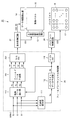
- FIG. 1 It is a figure which shows the display position in the liquid crystal display device which does not perform a double speed process, and the image on a retina. It is a figure which shows the display position and image on a retina in the liquid crystal display device shown in FIG. It is a block diagram which shows the structure of the liquid crystal display device which concerns on the 4th Embodiment of this invention. It is a block diagram which shows the structure of the conventional liquid crystal display device.
- FIG. 1 is a block diagram showing the configuration of the liquid crystal display device according to the first embodiment of the present invention.
- a liquid crystal display device 10 shown in FIG. 1 includes a field sequential processing unit 11, a display control circuit 12, a scanning line driving circuit 13, a data line driving circuit 14, a liquid crystal panel 15, a backlight control circuit 16, and a backlight 17. ing.
- the liquid crystal display device 10 displays four fields (white, red, green, and blue fields) in one frame period by performing field sequential driving. Further, the liquid crystal display device 10 controls the luminance of the backlight 17 for each region according to the input video data.
- m and n are integers of 2 or more
- p and q are integers of 1 or more
- p ⁇ m and q ⁇ n are satisfied.
- the liquid crystal panel 15 includes a plurality of pixels arranged two-dimensionally. More specifically, the liquid crystal panel 15 includes m scanning lines (not shown), n data lines (not shown), and (m ⁇ n) pixels (not shown). Yes.
- the m scanning lines extend in the horizontal direction (lateral direction in FIG. 1) of the display screen and are arranged in parallel to each other.
- the n data lines extend in the vertical direction (vertical direction in FIG. 1) of the display screen, and are arranged in parallel to each other so as to be orthogonal to the m scanning lines.
- (M ⁇ n) pixels are arranged corresponding to the intersections of m scanning lines and n data lines.
- the display control circuit 12 outputs a control signal CS1 to the scanning line driving circuit 13, and outputs a control signal CS2 and a video signal VS to the data line driving circuit 14.
- the scanning line driving circuit 13 sequentially selects m scanning lines based on the control signal CS1.
- the data line driving circuit 14 applies a voltage according to the video signal VS to the n data lines based on the control signal CS2.
- the backlight 17 includes a plurality of types of light sources (red, green, and blue light sources) having different emission colors. More specifically, the backlight 17 is a direct type backlight including a plurality of LEDs (Light Emitting Diodes) 18 arranged two-dimensionally. Among the plurality of LEDs 18, a red LED, a green LED, and a blue LED are included. As shown in FIG. 2, there are p backlights 17 in the vertical direction (vertical direction in FIG. 2) of the display screen, q in the horizontal direction (horizontal direction in FIG. 2) of the display screen, and (p ⁇ q) in total. It is divided into a plurality of regions 19. The liquid crystal panel 15 is similarly divided into (p ⁇ q) regions.
- LEDs Light Emitting Diodes
- Each region 19 includes at least one red LED, green LED, and blue LED. Each region 19 may include one red LED, one green LED, and one blue LED.
- the backlight control circuit 16 outputs a control signal CS3 to the backlight 17.
- the control signal CS3 indicates the luminance of the LED 18 in each area 19.
- the LEDs 18 in each region 19 emit light with the same luminance according to the control signal CS3.
- the liquid crystal display device 10 receives input video data including three color component data (red video data Ri, green video data Gi, and blue video data Bi) from the outside.
- red video data Ri, green video data Gi, and blue video data Bi the frame rate of the input video data is 60 Hz.
- FIG. 1 three video data Ri, Gi, Bi are described as being input separately, but three video data Ri, Gi, Bi may be input in a mixed manner.
- the input video data is supplied to the field sequential processing unit 11.
- the field sequential processing unit 11 includes a representative value calculation unit 111, a backlight data generation unit 112, a video data correction unit 113, a field data generation unit 114, a frame memory 115, and a buffer memory 116.
- the representative value calculation unit 111 obtains a representative value for each pixel of the liquid crystal panel 15 based on the input video data.
- the representative value calculation unit 111 may obtain, for example, the maximum values of the red video data Ri, the green video data Gi, and the blue video data Bi as the representative values for each pixel.
- the representative value calculation unit 111 may obtain an average value (simple average value or weighted average value) of the red video data Ri, the green video data Gi, and the blue video data Bi as a representative value for each pixel.
- the representative value calculation unit 111 outputs representative value data Xa indicating a representative value for each pixel.
- the number of data included in the representative value data Xa for one frame is equal to the number of pixels (m ⁇ n) of
- the backlight data generation unit 112 obtains the brightness of the LEDs 18 in each area 19 of the backlight 17 based on the representative value data Xa. For example, the backlight data generation unit 112 may obtain an average value of representative values for each pixel for each region 19 and obtain the luminance of the LED 18 in the region 19 based on the obtained average value. Alternatively, the backlight data generating unit 112 may obtain the maximum representative value for each pixel for each region 19 and obtain the luminance of the LED 18 in the region 19 based on the obtained maximum value. The backlight data generation unit 112 outputs backlight data Xb indicating the luminance of the LEDs 18 in each area 19 of the backlight 17. The number of data included in one frame of backlight data Xb is equal to the number of areas 19 (p ⁇ q). The backlight data Xb is stored in the buffer memory 116 and supplied to the video data correction unit 113.
- the video data correction unit 113 corrects the input video data based on the backlight data Xb. For example, the video data correction unit 113 obtains the luminance of the backlight 17 at the position of each pixel of the liquid crystal panel 15 based on the backlight data Xb, and divides the luminance of each pixel by the luminance of the backlight 17 at the position of the pixel. Thus, the three pieces of video data Ri, Gi, Bi are corrected. The video data correction unit 113 outputs corrected red video data Rc, corrected green video data Gc, and corrected blue video data Bc as corrected video data.
- the field data generation unit 114 has four field data (white field data Wf, red field data Rf) more than the types of light sources included in the backlight 17 based on the three corrected video data Rc, Gc, and Bc. , Green field data Gf and blue field data Bf).
- the field data generation unit 114 performs calculations represented by the following equations (1) to (4) for each pixel of the liquid crystal panel 15. Note that min represents an operation for obtaining a minimum value.
- Wf min (Rc, Gc, Bc) (1)
- Rf Rc ⁇ Wf (2)
- Gf Gc ⁇ Wf (3)
- Bf Bc ⁇ Wf (4)
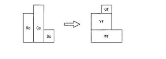
- FIG. 3 is a diagram illustrating an example of processing in the field data generation unit 114.
- three rectangles described on the left side of the arrow represent corrected video data, and three rectangles described on the right side of the arrow represent field data.
- Bc ⁇ Rc ⁇ Gc is established.
- Wf Bc
- Rf Rc ⁇ Bc
- Gf Gc ⁇ Bc
- Bf 0.
- the four field data Wf, Rf, Gf, and Bf generated by the field data generation unit 114 are stored in the frame memory 115.
- the display control circuit 12 sequentially reads the four field data Wf, Rf, Gf, and Bf stored in the frame memory 115.
- the backlight control circuit 16 reads the backlight data Xb stored in the buffer memory 116.
- the liquid crystal panel 15 is driven based on the four field data Wf, Rf, Gf, and Bf, and the backlight 17 is controlled based on the backlight data Xb.
- FIG. 4 is a timing chart of the liquid crystal display device 10.
- one frame period is divided into four field periods (white, red, green, and blue field periods).
- video data RGB1 of the first frame is input to the liquid crystal display device 10.
- the field sequential processing unit 11 generates backlight data X1 and four field data W1, R1, G1, and B1 based on the video data RGB1 of the first frame.
- the backlight data X1 is stored in the buffer memory 116, and the four field data W1, R1, G1, and B1 are stored in the frame memory 115.
- the display control circuit 12 sequentially reads four field data W1, R1, G1, and B1 from the frame memory 115, and outputs a video signal VS including the read field data to the data line driving circuit 14. .
- the scanning line driving circuit 13 and the data line driving circuit 14 are based on white, red, green, and blue field data W1, R1, G1, and B1, respectively, in the white, red, green, and blue field periods.
- the liquid crystal panel 15 is driven.
- the backlight control circuit 16 reads the backlight data X1 from the buffer memory 116 in the second frame period.
- the backlight control circuit 16 controls one or three types of LEDs corresponding to the field color to be in a light emission state in each field period. Specifically, the backlight control circuit 16 controls the red, green, and blue LEDs to emit light during the white field period, and red, green, and blue respectively during the red, green, and blue field periods. And blue LED is controlled to a light emission state. In any field period, the backlight control circuit 16 performs control so that the LEDs 18 in each area 19 emit light with a luminance corresponding to the backlight data X1.
- the field sequential processing unit 11 is based on the input video data, and the four field data Wf, Rf, Gg, Bf used for driving the liquid crystal panel 15 and the backlight used for controlling the backlight 17.
- Data Xb is generated.
- the display control circuit 12, the scanning line driving circuit 13, and the data line driving circuit 14 function as a panel driving circuit that drives the liquid crystal panel 15 based on field data corresponding to the field color in each field period.
- the backlight control circuit 16 controls one or more light sources corresponding to the color of the field to a light emission state based on the backlight data Xb.
- the liquid crystal display device 10 it is possible to display a color image by displaying white, red, green, and blue fields in one frame period. Further, by displaying the white field in addition to the red, green, and blue fields, each of red, green, and blue can be displayed in two fields, and color breakup can be reduced. Further, by controlling the luminance of the backlight 17 for each region according to the input video data, the power consumption of the backlight 17 can be reduced and the power consumption of the liquid crystal display device 10 can be reduced.
- a field sequential type liquid crystal display device that controls the luminance of the backlight for each region and displays white, red, green, and blue fields.
- a liquid crystal display device can be configured using, for example, a field sequential processing unit 90 shown in FIG. In FIG. 5, an RGB / WRGB conversion unit 91 converts three pieces of video data Ri, Gi, Bi into four field data Wa, Ra, Ga, Ba.
- the four backlight data generation units 92 generate backlight data Wx, Rx, Gx, and Bx indicating the luminance for each backlight region based on the field data Wa, Ra, Ga, and Ba, respectively.
- the four field data correction units 93 correct the field data Wa, Ra, Ga, Ba based on the backlight data Wx, Rx, Gx, Bx, respectively, and the corrected field data Wf, Rf, Gf, Bf Is output.
- the field sequential processing unit 90 generates the backlight data and corrects the field data after adding the white field. For this reason, the field sequential processing unit 90 needs to obtain the luminance of the backlight for each of the white, red, green, and blue fields. Therefore, the liquid crystal display device provided with the field sequential processing unit 90 has a problem that the circuit scale for obtaining the luminance of the backlight for each region is large.
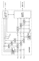
- the image display device (FIG. 15) described in Patent Document 1 adds a white field after generating backlight data and correcting video data. For this reason, in this image display device, it is not necessary to obtain the luminance of the backlight for the white field. However, this image display apparatus obtains the brightness of the backlight for each of the red, green, and blue fields individually. Therefore, this image display device also has a problem that the scale of the circuit for obtaining the luminance of the backlight for each region is large.
- the field sequential processing unit 11 of the liquid crystal display device 10 is based on the representative value calculation unit 111 that obtains a representative value for each pixel based on input video data, and the representative value obtained by the representative value calculation unit 111.
- the video data correction unit 113 that corrects the input video data based on the backlight data Xb, and the corrected input video data obtained by the video data correction unit 113.
- a field data generation unit 114 that generates four field data Wf, Rf, Gf, and Bf.
- the field sequential processing unit 11 generates the backlight data Xb based on the representative value for each pixel of the input video data, adds the white field after generating the backlight data Xb and correcting the input video data.
- the backlight data Xb is not generated individually for each of a plurality of color component data, but is generated based on the representative value for each pixel of the input video data. .
- the amount of calculation for obtaining the luminance of the backlight 17 for each region is 1 ⁇ 4 that of the liquid crystal display device provided with the field sequential processing unit 90 shown in FIG. 5, and the image display device shown in FIG. 1/3 of the case. Therefore, according to the liquid crystal display device 10 according to the present embodiment, the amount of calculation for obtaining the luminance of the backlight 17 for each region is reduced, and the scale of the circuit for obtaining the luminance of the backlight 17 for each region is reduced. Can do.
- the representative value calculation unit 111 may obtain a maximum value of a plurality of color component data as a representative value for each pixel, or may obtain an average value of the plurality of color component data. In any case, the circuit scale for obtaining the luminance of the backlight 17 for each region can be reduced.
- FIG. 6 is a block diagram showing a configuration of a liquid crystal display device according to the second embodiment of the present invention.
- the liquid crystal display device 20 illustrated in FIG. 6 includes a field sequential processing unit 21, a display control circuit 22, a scanning line driving circuit 13, a data line driving circuit 14, a liquid crystal panel 15, a backlight control circuit 23, and a backlight 17. ing.
- the liquid crystal display device 20 displays seven fields (white, cyan, yellow, magenta, red, green, and blue fields) in one frame period by performing field sequential driving.
- the same constituent elements as those of the above-described embodiments and constituent elements having the same functions and different operation speeds are denoted by the same reference numerals and description thereof is omitted. .
- the field sequential processing unit 21 includes a representative value calculation unit 111, a backlight data generation unit 112, a video data correction unit 113, a field data generation unit 211, a frame memory 212, and a buffer memory 116.
- the field data generation unit 211 generates seven field data (white field data Wf, cyan field data Cf, yellow field data) based on the three corrected video data Rc, Gc, and Bc output from the video data correction unit 113.
- the field data generation unit 211 performs calculations represented by the following equations (5) to (11) for each pixel of the liquid crystal panel 15.
- Wf min (Rc, Gc, Bc) (5)
- Cf min (Gc ⁇ Wf, Bc ⁇ Wf) (6)
- Yf min (Rc ⁇ Wf, Gc ⁇ Wf) (7)
- Mf min (Rc ⁇ Wf, Bc ⁇ Wf) (8)
- Rf Rc ⁇ Wf ⁇ Yf ⁇ Mf (9)
- Gf Gc ⁇ Wf ⁇ Cf ⁇ Yf (10)
- Bf Bc ⁇ Wf ⁇ Cf ⁇ Mf (11)
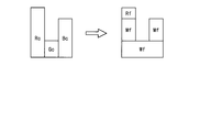
- FIG. 7A to 7C are diagrams illustrating an example of processing in the field data generation unit 211.
- the seven field data Wf, Cf, Yf, Mf, Rf, Gf, and Bf generated by the field data generation unit 211 are stored in the frame memory 212.
- the display control circuit 22 sequentially reads the seven field data Wf, Cf, Yf, Mf, Rf, Gf, and Bf stored in the frame memory 212.
- the backlight control circuit 23 reads the backlight data Xb stored in the buffer memory 116.
- the liquid crystal panel 15 is driven based on seven field data Wf, Cf, Yf, Mf, Rf, Gf, and Bf, and the backlight 17 is controlled based on the backlight data Xb.
- FIG. 8 is a timing chart of the liquid crystal display device 20.
- one frame period is divided into seven field periods (white, cyan, yellow, magenta, red, green, and blue field periods).
- video data RGB1 of the first frame is input to the liquid crystal display device 20.
- the field sequential processing unit 21 generates backlight data X1 and seven field data W1, C1, Y1, M1, R1, G1, and B1 based on the video data RGB1 of the first frame.
- the backlight data X1 is stored in the buffer memory 116, and the seven field data W1, C1, Y1, M1, R1, G1, and B1 are stored in the frame memory 212.
- the display control circuit 22 sequentially reads seven field data W1, C1, Y1, M1, R1, G1, and B1 from the frame memory 212 within the second frame period, and receives the video signal VS including the read field data as data. Output to the line drive circuit 14.
- the scanning line driving circuit 13 and the data line driving circuit 14 are respectively white, cyan, yellow, magenta, red, green, and blue in the white, cyan, yellow, magenta, red, green, and blue fields.
- the liquid crystal panel 15 is driven based on the field data W1, C1, Y1, M1, R1, G1, and B1.
- the backlight control circuit 23 reads the backlight data X1 from the buffer memory 116 in the second frame period.
- the backlight control circuit 23 controls the red, green, and blue LEDs to emit light during the white field period, controls the green and blue LEDs to emit light during the cyan field period, and red and green during the yellow field period. LEDs are controlled to emit light, red and blue LEDs are controlled to emit light during the magenta field period, and red, green, and blue LEDs emit light during the red, green, and blue field periods, respectively. Control to the state. In any field period, the backlight control circuit 23 controls the LEDs 18 in each area 19 to emit light with a luminance corresponding to the backlight data X1.
- the backlight data Xb is generated based on the representative value for each pixel of the input video data, as in the first embodiment. Therefore, according to the liquid crystal display device 20, as in the first embodiment, it is possible to reduce the scale of a circuit for obtaining the luminance of the backlight 17 for each region. Further, according to the liquid crystal display device 20, in addition to the red, green, and blue fields, the white, cyan, yellow, and magenta fields are displayed, so that red, green, and blue are respectively displayed. It is possible to reduce the color breakup by displaying in a field of sheets.
- a liquid crystal display device that displays 4 to 6 fields in one frame period can be configured by performing field sequential driving.
- FIG. 9 is a block diagram showing a configuration of a liquid crystal display device that displays four fields (yellow, red, green, and blue fields) in one frame period.
- the field data generation unit 261 is based on three corrected video data Rc, Gc, and Bc, and four field data (yellow field data Yf, red field data Rf, green field data Gf, and Blue field data Bf) is generated.
- the field data generation unit 261 performs calculations represented by the following equations (12) to (15) for each pixel of the liquid crystal panel 15.
- Yf min (Rc, Gc) (12)
- Rf Rc ⁇ Yf (13)
- Gf Gc ⁇ Yf (14)
- Bf Bc (15)
- the display control circuit 27 sequentially reads the four field data Yf, Rf, Gf, and Bf stored in the frame memory 262.
- the scanning line driving circuit 13 and the data line driving circuit 14 are based on yellow, red, green, and blue field data Y1, R1, G1, and B1, respectively, in the yellow, red, green, and blue field periods.
- the liquid crystal panel 15 is driven.
- the backlight control circuit 28 reads the backlight data Xb stored in the buffer memory 116.
- the backlight control circuit 28 controls the red and green LEDs to emit light during the yellow field period, and sets the red, green, and blue LEDs to emit light during the red, green, and blue field periods, respectively. Control.
- the backlight data Xb is generated based on the representative value for each pixel of the input video data. Therefore, according to the liquid crystal display device 25, the scale of the circuit for obtaining the luminance of the backlight 17 for each region can be reduced. Further, by displaying the yellow field in addition to the red, green, and blue fields, red and green can be displayed in two fields, respectively, and color breakup can be reduced.
- the field data generation unit is selected from red, green, and blue field data and white, cyan, yellow, and magenta based on the three corrected video data Rc, Gc, and Bc. Field data of one color or more.
- a field of one or more colors selected from white, cyan, yellow, and magenta By displaying, two or more colors of red, green, and blue can be displayed in a plurality of fields, respectively, and color breakup can be reduced.
- the field data generation unit is selected from red, green, and blue field data, cyan, yellow, and magenta based on the three corrected video data Rc, Gc, and Bc. Color field data may be generated.
- the liquid crystal display device provided with such a field data generation unit, in addition to red, green, and blue fields, any one of cyan, yellow, and magenta is displayed, so that red, Two colors of green and blue can be displayed in two fields, respectively, and color breakup can be reduced.
- FIG. 10 is a block diagram showing a configuration of a liquid crystal display device according to the third embodiment of the present invention.
- a liquid crystal display device 30 shown in FIG. 10 includes a double speed processing unit 31, a field sequential processing unit 32, a display control circuit 12, a scanning line driving circuit 13, a data line driving circuit 14, a liquid crystal panel 15, a backlight control circuit 16, and A backlight 17 is provided.
- Input video data having a frame rate of 60 Hz is input to the liquid crystal display device 30 from the outside.
- the double speed processing unit 31 is provided in front of the field sequential processing unit 32.
- the double speed processing unit 31 doubles the frame rate of the input video data.
- the double speed processing unit 31 performs an interpolation process on two consecutive frames, and inserts the obtained interpolation frame between the two frames.
- the double speed processing unit 31 outputs the double speed video data having a frame rate of 120 Hz, including the red video data Rd, the green video data Gd, and the blue video data Bd.
- the double speed processing unit 31 is an example of a frame rate conversion unit that converts the frame rate of input video data.
- the field sequential processing unit 32 includes a representative value calculation unit 311, a backlight data generation unit 312, a video data correction unit 313, a field data generation unit 314, a frame memory 115, and a buffer memory 116.
- the field sequential processing unit 32 is supplied with the double-speed video data output from the double-speed processing unit 31.
- the representative value calculation unit 311 obtains a representative value for each pixel based on the double-speed video data, and the backlight data generation unit 312 generates the backlight data Xb based on the representative value for each pixel.
- the representative value calculation unit 311 calculates a representative value for each pixel based on the double-speed video data for one frame, and the backlight data generation unit 312 Backlight data Xb is generated based on the representative value for each pixel.
- the representative value calculation unit 311 and the backlight data generation unit 312 perform the above processing on the double-speed video data of the odd-numbered frame.
- the video data correction unit 313 corrects the red video data Rd, the green video data Gd, and the blue video data Bd based on the backlight data Xb.
- the video data correction unit 313 corrects the double-speed video data of the odd-numbered frame based on the backlight data Xb generated based on the frame, and generates the double-speed video data of the even-numbered frame based on the previous odd-numbered frame. Correction is performed based on the backlight data Xb.
- the field data generation unit 314 is based on the double-speed video data after correction for two frames obtained by the video data correction unit 313, and includes four field data (white field data Wf, red field data Rf, green field data Gf, and , Blue field data Bf).
- FIG. 11 is a timing chart of the first example of the liquid crystal display device 30.
- one frame period is divided into white, red, green, and blue field periods in order from the front.
- the double speed processing unit 31 supplies the field sequential processing unit 32 with the double-speed video data RGBD1 of the first frame in the first half of the first frame period, and the double-speed video data RGBD2 of the second frame in the second half of the first frame period. Supply.
- the representative value calculation unit 311 obtains a representative value for each pixel based on the double-speed video data RGBD1 of the first frame.
- the backlight data generation unit 312 generates the backlight data X1 based on the representative value for each pixel of the double-speed video data RGBD1 of the first frame.
- the video data correction unit 313 corrects the double-speed video data RGBD1 of the first frame based on the backlight data X1.
- the field data generation unit 314 generates only the white field data W1 based on the corrected double-speed video data of the first frame.
- the white field data W1 is stored in the frame memory 115.
- the video data correction unit 313 corrects the double-speed video data RGBD2 of the second frame based on the previously generated backlight data X1.
- the field data generation unit 314 generates red field data R2, green field data G2, and blue field data B2 based on the double-speed video data after the second frame correction.
- the white field data W2 generated at this time is discarded.
- the red field data R2, the green field data G2, and the blue field data B2 are stored in the frame memory 115.
- the field data generation unit 314 generates the white field data W1 previously generated instead of generating the white field data W2 when generating the red field data R2, the green field data G2, and the blue field data B2. May be used.
- FIG. 12 is a timing chart of the second example of the liquid crystal display device 30.
- one frame period is divided into green, blue, white, and red field periods in order from the front.
- the representative value calculation unit 311, the backlight data generation unit 312, and the video data correction unit 313 operate in the same manner as in the first example.
- the field data generation unit 314 In the first half of the first frame period, the field data generation unit 314 generates white field data W1 and red field data R1 based on the corrected double-speed video data of the first frame.
- the field data generation unit 314 In the second half of the first frame period, the field data generation unit 314 generates green field data G2 and blue field data B2 based on the corrected double-speed video data of the second frame.
- FIG. 11 and 12 show the storage location of each field data in the frame memory 115.
- the white field data W1 is stored in the fifth area M5 of the frame memory 115
- the red field data R2 is stored in the sixth area M6 of the frame memory 115.
- a memory capable of storing field data for 8 frames is required as the frame memory 115.
- a memory capable of storing field data for 6 frames can be used as the frame memory 115.
- the capacity of the frame memory 115 can be reduced as compared with the first example.
- the liquid crystal display device 30 includes a double speed processing unit 31 that doubles the frame rate of the input video data.
- the field sequential processing unit 32 is supplied with the double speed video data output from the double speed processing unit 31. Therefore, according to the liquid crystal display device 30, in the field sequential type liquid crystal display device that performs double speed processing on the input video data and controls the luminance of the backlight for each region according to the double speed video data, the luminance of the backlight 17 is set. The scale of the circuit required for each area can be reduced.
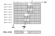
- FIG. 13A is a diagram showing a display position and an image on the retina in a liquid crystal display device that does not perform double speed processing.
- the display positions in the four fields are the same. For this reason, when the observer's line of sight moves following the object in the display screen, the observer may see the field colors separated at the ends A1 and A2 of the object. For example, the end A1 may appear red and the end A2 may appear blue.
- FIG. 13B is a diagram showing a display position on the liquid crystal display device 30 and an image on the retina.
- the display position in the white field is shifted from the display position in the red, green, and blue fields. For this reason, even when the observer's line of sight moves following the object in the display screen, the observer is less likely to see the colors of the field separated at the edge of the object.
- the liquid crystal display device 30 by performing the double speed process, which is an example of the frame rate conversion process, on the input video data, it is possible to correct the display position in the field and reduce the color breakup.
- the liquid crystal drive frequency is 480 Hz. It is difficult or expensive to drive the liquid crystal at a frame rate of 480 Hz.
- the representative value calculation unit 311 obtains a representative value for each pixel based on the double-speed video data for one frame.
- the backlight data generation unit 312 generates backlight data Xb based on the representative value for one frame
- the video data correction unit 313 corrects double-speed video data for two frames based on the backlight data Xb to generate field data.
- the unit 314 generates four pieces of field data corresponding to one frame period based on the corrected video data for two frames obtained by the video data correction unit 313.
- the driving frequency of the liquid crystal is 240 Hz. Driving the liquid crystal at a frame rate of 240 Hz is easier or less expensive than driving the liquid crystal at a frame rate of 480 Hz.
- the liquid crystal display device 30 can be configured easily or at low cost by lowering the driving frequency of the liquid crystal. Further, the frame rate conversion unit can be easily configured by using the double speed processing unit 31.
- FIG. 14 is a block diagram showing a configuration of a liquid crystal display device 40 according to the fourth embodiment of the present invention.
- a liquid crystal display device 40 shown in FIG. 14 is obtained by replacing the double speed processing unit 31 with a frame rate conversion unit 41 in the liquid crystal display device 30 according to the third embodiment.
- Input video data having a frame rate of 60 Hz is input to the liquid crystal display device 40 from the outside.
- the frame rate conversion unit 41 is provided in front of the field sequential processing unit 32.
- the frame rate conversion unit 41 performs a frame rate conversion process on the input video data, and raises the frame rate of the input video data from 60 Hz to 144 Hz.
- the frame rate conversion unit 41 includes red video data Re, green video data Ge, and blue video data Be, and outputs frame rate converted video data having a frame rate of 144 Hz.
- the field sequential processing unit 32 is supplied with the frame rate converted video data output from the frame rate conversion unit 41.
- the field sequential processing unit 32 operates in the same manner as in the third embodiment.
- the liquid crystal display device 40 includes a frame rate conversion unit 41 that performs frame rate conversion processing on input video data, and the field sequential processing unit 32 is supplied with the video data after frame rate conversion output from the frame rate conversion unit 41. Is done. Therefore, according to the liquid crystal display device 40, in the field sequential type liquid crystal display device that controls the luminance of the backlight for each region in accordance with the video data after the frame rate conversion, the circuit for obtaining the luminance of the backlight 17 for each region. Can reduce the scale.
- the frame rate conversion process is performed on the input video data, thereby correcting the display position in the field and reducing the color breakup.
- the liquid crystal display device 40 can be configured easily or at low cost by lowering the driving frequency of the liquid crystal.
- the frame rate of the display screen is 72 Hz
- the driving frequency of the liquid crystal is 288 Hz.
- the frame rate of the display screen is set to 70 Hz or higher, it becomes difficult for an observer to recognize flicker generated on the display screen.
- the driving frequency of the liquid crystal is 288 Hz
- a practical and low-cost liquid crystal panel can be used as the liquid crystal panel 15. Therefore, according to the liquid crystal display device 40, flicker generated on the display screen can be suppressed using a practical and low-cost liquid crystal panel.
- the liquid crystal display device described above includes a direct-type backlight including a plurality of LEDs 18 arranged two-dimensionally as the backlight 17.
- the liquid crystal display device of the present invention may include an edge light type backlight including a plurality of LEDs and a light guide plate arranged one-dimensionally as the backlight 17.
- liquid crystal display device of the present invention in the field sequential type liquid crystal display device that controls the luminance of the backlight for each region according to the video data, based on the representative value for each pixel of the video data.
- the backlight data By generating the backlight data, it is possible to reduce the scale of the circuit for obtaining the backlight luminance for each region.
- the liquid crystal display device of the present invention has a feature that the scale of a circuit for obtaining the luminance of the backlight for each region can be reduced, so that it can be used for display portions of various electronic devices.
Landscapes
- Engineering & Computer Science (AREA)
- Physics & Mathematics (AREA)
- Computer Hardware Design (AREA)
- General Physics & Mathematics (AREA)
- Theoretical Computer Science (AREA)
- Chemical & Material Sciences (AREA)
- Crystallography & Structural Chemistry (AREA)
- Liquid Crystal Display Device Control (AREA)
- Control Of Indicators Other Than Cathode Ray Tubes (AREA)
- Liquid Crystal (AREA)
Abstract
フィールドシーケンシャル処理部11は、映像データRi、Gi、Biに基づき画素ごとの代表値を求める代表値算出部111と、求めた代表値に基づきバックライト17の各領域内のLED18の輝度を示すバックライトデータXbを生成するバックライトデータ生成部112と、バックライトデータXbに基づき映像データRi、Gi、Biを補正する映像データ補正部113と、補正後の映像データRc、Gc、Bcに基づき4個のフィールドデータWf、Rf、Gf、Bfを生成するフィールドデータ生成部114とを含む。画素ごとの代表値に基づきバックライトデータを生成することにより、バックライトの輝度を領域ごとに求める回路の規模を削減する。
Description
本発明は、液晶表示装置に関し、より詳細には、フィールドシーケンシャル方式の液晶表示装置、および、その駆動方法に関する。
液晶表示装置は、カラー画像を表示する画像表示装置として広く利用されている。従来の多くの液晶表示装置は、カラーフィルタを用いてカラー画像を表示する。また、カラーフィルタを用いずにカラー画像を表示する液晶表示装置として、フィールドシーケンシャル方式の液晶表示装置が知られている。
典型的なフィールドシーケンシャル方式の液晶表示装置は、赤、緑、および、青の光源を含むバックライトを備え、1フレーム期間に赤、緑、および、青の3枚のフィールドを表示する。赤フィールドを表示するときには、液晶パネルは赤映像データに基づき駆動され、赤色光源が発光する。続いて、緑フィールドと青フィールドが同様の方法で表示される。時分割で表示された3枚のフィールドは、観測者の網膜上で残像現象によって合成され、観測者には1枚のカラー画像として認識される。
フィールドシーケンシャル方式の液晶表示装置では、観測者の視線が表示画面内を移動したときに、観測者に3枚のフィールドの色が分離して見えることがある。この現象は、色割れと呼ばれる。色割れを低減する方法として、赤、緑、および、青のフィールドに加えて白フィールドを表示する方法が従来から知られている。これとは別に、液晶表示装置の消費電力を削減する方法として、映像データに応じてバックライトの輝度を領域ごとに制御する方法が知られている。
特許文献1には、バックライトの輝度を領域ごとに制御し、白、赤、緑、および、青のフィールドを表示する画像表示装置が記載されている(図15を参照)。図15に示す画像表示装置は、入力映像信号Rorg、Gorg、Borgに対して低解像度化処理を行うことにより、バックライトの部分発光領域単位での発光パターンBLr、BLg、BLbを求める。次にこの画像表示装置は、入力映像信号Rorg、Gorg、Borgを発光パターンBLr、BLg、BLbに拡散処理を行った結果で除算することにより部分駆動用映像信号R、G、Bを生成し、部分駆動用映像信号R、G、Bから共通白成分Wcomを抽出する。特許文献2には、映像信号の1フレームを単色光源の色の数よりも多いフィールドに分解するフィールドシーケンシャル映像表示装置が記載されている。
しかしながら、特許文献1に記載された画像表示装置は、バックライトの各部分発光領域について、赤フィールドの発光パターンBLr、緑フィールドの発光パターンBLg、および、青フィールドの発光パターンBLgを個別に求める。このため、この画像表示装置には、バックライトの輝度を領域ごとに求める回路の規模が大きいという問題がある。
それ故に、本発明は、バックライトの輝度を領域ごとに制御するフィールドシーケンシャル方式の液晶表示装置について、バックライトの輝度を領域ごとに求める回路の規模を削減することを目的とする。
本発明の第1の局面は、フィールドシーケンシャル方式の液晶表示装置であって、
2次元状に配置された複数の画素を含む液晶パネルと、
発光色が異なる複数種類の光源を複数個ずつ含むバックライトと、
複数の色成分データを含む映像データに基づき、前記液晶パネルの駆動に使用される複数のフィールドデータと、前記バックライトの制御に使用されるバックライトデータとを生成するフィールドシーケンシャル処理部と、
各フィールド期間において、フィールドの色に応じたフィールドデータに基づき前記液晶パネルを駆動するパネル駆動回路と、
各フィールド期間において、フィールドの色に応じた1種類以上の光源を前記バックライトデータに基づき発光状態に制御するバックライト制御回路とを備え、
前記フィールドシーケンシャル処理部は、
前記映像データに基づき画素ごとの代表値を求める代表値算出部と、
前記代表値算出部で求めた代表値に基づき、前記バックライトを複数の領域に分割したときの各領域内の光源の輝度を示すバックライトデータを生成するバックライトデータ生成部と、
前記バックライトデータに基づき前記映像データを補正する映像データ補正部と、
前記映像データ補正部で求めた補正後の映像データに基づき、前記光源の種類よりも多い複数のフィールドデータを生成するフィールドデータ生成部とを含むことを特徴とする。
2次元状に配置された複数の画素を含む液晶パネルと、
発光色が異なる複数種類の光源を複数個ずつ含むバックライトと、
複数の色成分データを含む映像データに基づき、前記液晶パネルの駆動に使用される複数のフィールドデータと、前記バックライトの制御に使用されるバックライトデータとを生成するフィールドシーケンシャル処理部と、
各フィールド期間において、フィールドの色に応じたフィールドデータに基づき前記液晶パネルを駆動するパネル駆動回路と、
各フィールド期間において、フィールドの色に応じた1種類以上の光源を前記バックライトデータに基づき発光状態に制御するバックライト制御回路とを備え、
前記フィールドシーケンシャル処理部は、
前記映像データに基づき画素ごとの代表値を求める代表値算出部と、
前記代表値算出部で求めた代表値に基づき、前記バックライトを複数の領域に分割したときの各領域内の光源の輝度を示すバックライトデータを生成するバックライトデータ生成部と、
前記バックライトデータに基づき前記映像データを補正する映像データ補正部と、
前記映像データ補正部で求めた補正後の映像データに基づき、前記光源の種類よりも多い複数のフィールドデータを生成するフィールドデータ生成部とを含むことを特徴とする。
本発明の第2の局面は、本発明の第1の局面において、
前記代表値算出部は、画素ごとの代表値として、前記複数の色成分データの最大値を求めることを特徴とする。
前記代表値算出部は、画素ごとの代表値として、前記複数の色成分データの最大値を求めることを特徴とする。
本発明の第3の局面は、本発明の第1の局面において、
前記代表値算出部は、画素ごとの代表値として、前記複数の色成分データの平均値を求めることを特徴とする。
前記代表値算出部は、画素ごとの代表値として、前記複数の色成分データの平均値を求めることを特徴とする。
本発明の第4の局面は、本発明の第1の局面において、
前記バックライトは、赤色光源、緑色光源、および、青色光源を複数個ずつ含み、
前記映像データは、赤映像データ、緑映像データ、および、青映像データを含み、
前記フィールドデータ生成部は、前記映像データ補正部で求めた補正後の赤映像データ、補正後の緑映像データ、および、補正後の青映像データに基づき、赤、緑、および、青のフィールドデータと、白、シアン、イエロー、および、マゼンタの中から選択された1色以上のフィールドデータとを生成することを特徴とする。
前記バックライトは、赤色光源、緑色光源、および、青色光源を複数個ずつ含み、
前記映像データは、赤映像データ、緑映像データ、および、青映像データを含み、
前記フィールドデータ生成部は、前記映像データ補正部で求めた補正後の赤映像データ、補正後の緑映像データ、および、補正後の青映像データに基づき、赤、緑、および、青のフィールドデータと、白、シアン、イエロー、および、マゼンタの中から選択された1色以上のフィールドデータとを生成することを特徴とする。
本発明の第5の局面は、本発明の第4の局面において、
前記フィールドデータ生成部は、白、赤、緑、および、青のフィールドデータを生成することを特徴とする。
前記フィールドデータ生成部は、白、赤、緑、および、青のフィールドデータを生成することを特徴とする。
本発明の第6の局面は、本発明の第4の局面において、
前記フィールドデータ生成部は、白、シアン、イエロー、マゼンタ、赤、緑、および、青のフィールドデータを生成することを特徴とする。
前記フィールドデータ生成部は、白、シアン、イエロー、マゼンタ、赤、緑、および、青のフィールドデータを生成することを特徴とする。
本発明の第7の局面は、本発明の第4の局面において、
前記フィールドデータ生成部は、赤、緑、および、青のフィールドデータと、シアン、イエロー、および、マゼンタの中から選択された1色のフィールドデータとを生成することを特徴とする。
前記フィールドデータ生成部は、赤、緑、および、青のフィールドデータと、シアン、イエロー、および、マゼンタの中から選択された1色のフィールドデータとを生成することを特徴とする。
本発明の第8の局面は、本発明の第1の局面において、
前記フィールドシーケンシャル処理部には、前記映像データとして、外部から入力された入力映像データが供給されることを特徴とする。
前記フィールドシーケンシャル処理部には、前記映像データとして、外部から入力された入力映像データが供給されることを特徴とする。
本発明の第9の局面は、本発明の第1の局面において、
外部から入力された入力映像データに対してフレームレート変換処理を行うフレームレート変換部をさらに備え、
前記フィールドシーケンシャル処理部には、前記映像データとして、前記フレームレート変換部から出力された変換後の映像データが供給されることを特徴とする。
外部から入力された入力映像データに対してフレームレート変換処理を行うフレームレート変換部をさらに備え、
前記フィールドシーケンシャル処理部には、前記映像データとして、前記フレームレート変換部から出力された変換後の映像データが供給されることを特徴とする。
本発明の第10の局面は、本発明の第9の局面において、
前記フレームレート変換部は、前記入力映像データのフレームレートを2倍にすることを特徴とする。
前記フレームレート変換部は、前記入力映像データのフレームレートを2倍にすることを特徴とする。
本発明の第11の局面は、本発明の第9の局面において、
2フレーム分の前記映像データが供給されたときに、前記代表値算出部は1フレーム分の前記映像データに基づき画素ごとの代表値を求め、前記バックライトデータ生成部は1フレーム分の代表値に基づき前記バックライトデータを生成し、前記映像データ補正部は前記バックライトデータに基づき2フレーム分の前記映像データを補正し、前記フィールドデータ生成部は前記映像データ補正部で求めた2フレーム分の補正後の映像データに基づき前記複数のフィールドデータを生成することを特徴とする。
2フレーム分の前記映像データが供給されたときに、前記代表値算出部は1フレーム分の前記映像データに基づき画素ごとの代表値を求め、前記バックライトデータ生成部は1フレーム分の代表値に基づき前記バックライトデータを生成し、前記映像データ補正部は前記バックライトデータに基づき2フレーム分の前記映像データを補正し、前記フィールドデータ生成部は前記映像データ補正部で求めた2フレーム分の補正後の映像データに基づき前記複数のフィールドデータを生成することを特徴とする。
本発明の第12の局面は、本発明の第11の局面において、
前記入力映像データのフレームレートは60Hzであり、
前記フレームレート変換部は、前記入力映像データのフレームレートを144Hzに変換し、
前記フィールドデータ生成部は、前記映像データ補正部で求めた2フレーム分の補正後の映像データに基づき4枚のフィールドデータを生成することを特徴とする。
前記入力映像データのフレームレートは60Hzであり、
前記フレームレート変換部は、前記入力映像データのフレームレートを144Hzに変換し、
前記フィールドデータ生成部は、前記映像データ補正部で求めた2フレーム分の補正後の映像データに基づき4枚のフィールドデータを生成することを特徴とする。
本発明の第13の局面は、2次元状に配置された複数の画素を含む液晶パネルと、発光色が異なる複数種類の光源を複数個ずつ含むバックライトとを含む、フィールドシーケンシャル方式の液晶表示装置の駆動方法であって、
複数の色成分データを含む映像データに基づき画素ごとの代表値を求めるステップと、
前記代表値に基づき、前記バックライトを複数の領域に分割したときの各領域内の光源の輝度を示すバックライトデータを求めるステップと、
前記バックライトデータに基づき前記映像データを補正するステップと、
補正後の映像データに基づき、前記光源の種類よりも多い複数のフィールドデータを生成するステップと、
各フィールド期間において、フィールドの色に応じたフィールドデータに基づき前記液晶パネルを駆動するステップと、
各フィールド期間において、フィールドの色に応じた1種類以上の光源を前記バックライトデータに基づき発光状態に制御するステップとを備える。
複数の色成分データを含む映像データに基づき画素ごとの代表値を求めるステップと、
前記代表値に基づき、前記バックライトを複数の領域に分割したときの各領域内の光源の輝度を示すバックライトデータを求めるステップと、
前記バックライトデータに基づき前記映像データを補正するステップと、
補正後の映像データに基づき、前記光源の種類よりも多い複数のフィールドデータを生成するステップと、
各フィールド期間において、フィールドの色に応じたフィールドデータに基づき前記液晶パネルを駆動するステップと、
各フィールド期間において、フィールドの色に応じた1種類以上の光源を前記バックライトデータに基づき発光状態に制御するステップとを備える。
本発明の第1または第13の局面によれば、映像データに応じてバックライトの輝度を領域ごとに制御するフィールドシーケンシャル方式の液晶表示装置において、バックライトデータは、映像データの画素ごとの代表値に基づき生成される。したがって、複数の色成分データに基づき複数のバックライトデータを個別に生成する場合と比べて、バックライトの輝度を領域ごとに求めるための演算量を削減し、バックライトの輝度を領域ごとに求める回路の規模を削減することができる。
本発明の第2の局面によれば、映像データの画素ごとの代表値として複数の色成分データの最大値を求め、求めた最大値に基づきバックライトデータを生成することにより、バックライトの輝度を領域ごとに求める回路の規模を削減することができる。
本発明の第3の局面によれば、映像データの画素ごとの代表値として複数の色成分データの平均値を求め、求めた平均値に基づきバックライトデータを生成することにより、バックライトの輝度を領域ごとに求める回路の規模を削減することができる。
本発明の第4の局面によれば、赤、緑、および、青のフィールドに加えて、白、シアン、イエロー、および、マゼンタの中から選択された1色以上のフィールドを表示することにより、赤、緑、および、青のうちの2色以上をそれぞれ複数のフィールドで表示し、色割れを低減することができる。
本発明の第5の局面によれば、赤、緑、および、青のフィールドに加えて白フィールドを表示することにより、赤、緑、および、青をそれぞれ2枚のフィールドで表示し、色割れを低減することができる。
本発明の第6の局面によれば、赤、緑、および、青のフィールドに加えて、白、シアン、イエロー、および、マゼンタのフィールドを表示することにより、赤、緑、および、青をそれぞれ4枚のフィールドで表示し、色割れを低減することができる。
本発明の第7の局面によれば、赤、緑、および、青のフィールドに加えて、シアン、イエロー、および、マゼンタのいずれかのフィールドを表示することにより、赤、緑、および、青のうちの2色をそれぞれ2枚のフィールドで表示し、色割れを低減することができる。
本発明の第8の局面によれば、入力映像データに応じてバックライトの輝度を領域ごとに制御するフィールドシーケンシャル方式の液晶表示装置において、入力映像データの画素ごとの代表値に基づきバックライトデータを生成することにより、バックライトの輝度を領域ごとに求める回路の規模を削減することができる。
本発明の第9の局面によれば、フレームレート変換後の映像データに応じてバックライトの輝度を領域ごとに制御するフィールドシーケンシャル方式の液晶表示装置において、フレームレート変換後の映像データの画素ごとの代表値に基づきバックライトデータを生成することにより、バックライトの輝度を領域ごとに求める回路の規模を削減することができる。また、入力映像データに対してフレームレート変換処理を行うことにより、フィールド内での表示位置を補正し、色割れを低減することができる。
本発明の第10の局面によれば、フレームレート変換部を容易に構成することができる。
本発明の第11の局面によれば、2フレーム分のフレームレート変換後の映像データに基づき1フレーム期間に対応した複数のフィールドを表示することにより、1フレーム分のフレームレート変換後の映像データに基づき1フレーム期間に対応した複数のフィールドを表示する場合と比べて、液晶の駆動周波数を低くして、液晶表示装置を容易あるいは低コストで構成することができる。
本発明の第12の局面によれば、表示画面のフレームレートを72Hz、液晶の駆動周波数を288Hzにすることにより、実用的で低コストの液晶パネルを用いて、表示画面に発生するフリッカを抑制することができる。
(第1の実施形態)
図1は、本発明の第1の実施形態に係る液晶表示装置の構成を示すブロック図である。図1に示す液晶表示装置10は、フィールドシーケンシャル処理部11、表示制御回路12、走査線駆動回路13、データ線駆動回路14、液晶パネル15、バックライト制御回路16、および、バックライト17を備えている。液晶表示装置10は、フィールドシーケンシャル駆動を行うことにより、1フレーム期間に4枚のフィールド(白、赤、緑、および、青のフィールド)を表示する。また、液晶表示装置10は、入力映像データに応じてバックライト17の輝度を領域ごとに制御する。以下、mおよびnは2以上の整数、pおよびqは1以上の整数であり、p<m、q<nを満たすとする。
図1は、本発明の第1の実施形態に係る液晶表示装置の構成を示すブロック図である。図1に示す液晶表示装置10は、フィールドシーケンシャル処理部11、表示制御回路12、走査線駆動回路13、データ線駆動回路14、液晶パネル15、バックライト制御回路16、および、バックライト17を備えている。液晶表示装置10は、フィールドシーケンシャル駆動を行うことにより、1フレーム期間に4枚のフィールド(白、赤、緑、および、青のフィールド)を表示する。また、液晶表示装置10は、入力映像データに応じてバックライト17の輝度を領域ごとに制御する。以下、mおよびnは2以上の整数、pおよびqは1以上の整数であり、p<m、q<nを満たすとする。
液晶パネル15は、2次元状に配置された複数の画素を含んでいる。より詳細には、液晶パネル15は、m本の走査線(図示せず)、n本のデータ線(図示せず)、および、(m×n)個の画素(図示せず)を含んでいる。m本の走査線は、表示画面の水平方向(図1では横方向)に延伸し、互いに平行に配置される。n本のデータ線は、表示画面の垂直方向(図1では縦方向)に延伸し、m本の走査線と直交するように互いに平行に配置される。(m×n)個の画素は、m本の走査線とn本のデータ線の交差点に対応して配置される。
表示制御回路12は、走査線駆動回路13に対して制御信号CS1を出力し、データ線駆動回路14に対して制御信号CS2と映像信号VSを出力する。走査線駆動回路13は、制御信号CS1に基づき、m本の走査線を順に選択する。データ線駆動回路14は、制御信号CS2に基づき、n本のデータ線に対して映像信号VSに応じた電圧を印加する。
バックライト17は、発光色が異なる複数種類の光源(赤、緑、および、青の光源)を複数個ずつ含んでいる。より詳細には、バックライト17は、2次元状に配置された複数のLED(Light Emitting Diode)18を含む直下型のバックライトである。複数のLED18の中には、赤色LED、緑色LED、および、青色LEDが含まれる。バックライト17は、図2に示すように、表示画面の垂直方向(図2では縦方向)にp個、表示画面の水平方向(図2では横方向)にq個、全部で(p×q)個の領域19に分割される。液晶パネル15も、同様に(p×q)個の領域に分割される。各領域19には、赤色LED、緑色LED、および、青色LEDが少なくとも1個ずつ含まれる。各領域19には、赤色LED、緑色LED、および、青色LEDが1個ずつ含まれていてもよい。バックライト制御回路16は、バックライト17に対して制御信号CS3を出力する。制御信号CS3は、各領域19内のLED18の輝度を示す。各領域19内のLED18は、制御信号CS3に従い同じ輝度で発光する。
液晶表示装置10には外部から、3個の色成分データ(赤映像データRi、緑映像データGi、および、青映像データBi)を含む入力映像データが入力される。以下、入力映像データのフレームレートは60Hzであるとする。なお、図1では3個の映像データRi、Gi、Biを別々に入力するように記載されているが、3個の映像データRi、Gi、Biを混在して入力してもよい。入力映像データは、フィールドシーケンシャル処理部11に供給される。
フィールドシーケンシャル処理部11は、代表値算出部111、バックライトデータ生成部112、映像データ補正部113、フィールドデータ生成部114、フレームメモリ115、および、バッファメモリ116を含んでいる。代表値算出部111は、入力映像データに基づき、液晶パネル15の画素ごとの代表値を求める。代表値算出部111は、画素ごとの代表値として、例えば、赤映像データRi、緑映像データGi、および、青映像データBiの最大値を求めてもよい。あるいは、代表値算出部111は、画素ごとの代表値として、赤映像データRi、緑映像データGi、および、青映像データBiの平均値(単純平均値または加重平均値)を求めてもよい。代表値算出部111は、画素ごとの代表値を示す代表値データXaを出力する。1フレーム分の代表値データXaに含まれるデータの個数は、液晶パネル15の画素数(m×n)に等しい。
バックライトデータ生成部112は、代表値データXaに基づき、バックライト17の各領域19内のLED18の輝度を求める。バックライトデータ生成部112は、例えば、画素ごとの代表値の平均値を領域19ごとに求め、求めた平均値に基づき領域19内のLED18の輝度を求めてもよい。あるいは、バックライトデータ生成部112は、画素ごとの代表値の最大値を領域19ごとに求め、求めた最大値に基づき領域19内のLED18の輝度を求めてもよい。バックライトデータ生成部112は、バックライト17の各領域19内のLED18の輝度を示すバックライトデータXbを出力する。1フレーム分のバックライトデータXbに含まれるデータの個数は、領域19の個数(p×q)に等しい。バックライトデータXbは、バッファメモリ116に記憶されると共に、映像データ補正部113に供給される。
映像データ補正部113は、バックライトデータXbに基づき、入力映像データを補正する。映像データ補正部113は、例えば、バックライトデータXbに基づき液晶パネル15の各画素の位置におけるバックライト17の輝度を求め、各画素の輝度を当該画素の位置におけるバックライト17の輝度で除算することにより、3個の映像データRi、Gi、Biを補正する。映像データ補正部113は、補正後の映像データとして、補正後の赤映像データRc、補正後の緑映像データGc、および、補正後の青映像データBcを出力する。
フィールドデータ生成部114は、3個の補正後の映像データRc、Gc、Bcに基づき、バックライト17に含まれる光源の種類よりも多い4個のフィールドデータ(白フィールドデータWf、赤フィールドデータRf、緑フィールドデータGf、および、青フィールドデータBf)を生成する。例えば、フィールドデータ生成部114は、液晶パネル15の各画素について、次式(1)~(4)に示す演算を行う。なお、minは最小値を求める演算を表す。
Wf=min(Rc,Gc,Bc) …(1)
Rf=Rc-Wf …(2)
Gf=Gc-Wf …(3)
Bf=Bc-Wf …(4)
Wf=min(Rc,Gc,Bc) …(1)
Rf=Rc-Wf …(2)
Gf=Gc-Wf …(3)
Bf=Bc-Wf …(4)
図3は、フィールドデータ生成部114における処理の例を示す図である。図3において、矢印の左に記載された3個の長方形は補正後の映像データを表し、矢印の右に記載された3個の長方形はフィールドデータを表す。図3に示す例では、Bc<Rc<Gcが成立する。この場合、式(1)~(4)より、Wf=Bc、Rf=Rc-Bc、Gf=Gc-Bc、Bf=0となる。
フィールドデータ生成部114で生成された4個のフィールドデータWf、Rf、Gf、Bfは、フレームメモリ115に記憶される。表示制御回路12は、フレームメモリ115に記憶された4個のフィールドデータWf、Rf、Gf、Bfを順に読み出す。バックライト制御回路16は、バッファメモリ116に記憶されたバックライトデータXbを読み出す。液晶パネル15は4個のフィールドデータWf、Rf、Gf、Bfに基づき駆動され、バックライト17はバックライトデータXbに基づき制御される。
図4は、液晶表示装置10のタイミングチャートである。液晶表示装置10では、1フレーム期間は、4個のフィールド期間(白、赤、緑、および、青のフィールド期間)に分割される。第1フレーム期間では、液晶表示装置10には第1フレームの映像データRGB1が入力される。フィールドシーケンシャル処理部11は、第1フレームの映像データRGB1に基づき、バックライトデータX1と4個のフィールドデータW1、R1、G1、B1を生成する。バックライトデータX1はバッファメモリ116に記憶され、4個のフィールドデータW1、R1、G1、B1はフレームメモリ115に記憶される。
表示制御回路12は、第2フレーム期間において、フレームメモリ115から4個のフィールドデータW1、R1、G1、B1を順に読み出し、読み出したフィールドデータを含む映像信号VSをデータ線駆動回路14に出力する。走査線駆動回路13とデータ線駆動回路14は、白、赤、緑、および、青のフィールド期間では、それぞれ、白、赤、緑、および、青のフィールドデータW1、R1、G1、B1に基づき液晶パネル15を駆動する。
バックライト制御回路16は、第2フレーム期間において、バッファメモリ116からバックライトデータX1を読み出す。バックライト制御回路16は、各フィールド期間において、フィールドの色に応じた1種類または3種類のLEDを発光状態に制御する。具体的には、バックライト制御回路16は、白フィールド期間では赤色、緑色、および、青色のLEDを発光状態に制御し、赤、緑、および、青のフィールド期間では、それぞれ、赤色、緑色、および、青色のLEDを発光状態に制御する。いずれのフィールド期間でも、バックライト制御回路16は、各領域19内のLED18がバックライトデータX1に応じた輝度で発光するように制御する。
このようにフィールドシーケンシャル処理部11は、入力映像データに基づき、液晶パネル15の駆動に使用される4個のフィールドデータWf、Rf、Gg、Bfと、バックライト17の制御に使用されるバックライトデータXbとを生成する。表示制御回路12、走査線駆動回路13、および、データ線駆動回路14は、各フィールド期間において、フィールドの色に応じたフィールドデータに基づき液晶パネル15を駆動するパネル駆動回路として機能する。バックライト制御回路16は、各フィールド期間において、フィールドの色に応じた1種類以上の光源をバックライトデータXbに基づき発光状態に制御する。
本実施形態に係る液晶表示装置10によれば、1フレーム期間に白、赤、緑、および、青のフィールドを表示することにより、カラー画像を表示することができる。また、赤、緑、および、青のフィールドに加えて白フィールドを表示することにより、赤、緑、および、青をそれぞれ2枚のフィールドで表示し、色割れを低減することができる。また、入力映像データに応じてバックライト17の輝度を領域ごとに制御することにより、バックライト17の消費電力を削減し、液晶表示装置10の消費電力を削減することができる。
以下、液晶表示装置10の特有の効果を説明する。ここで、バックライトの輝度を領域ごとに制御し、白、赤、緑、および、青のフィールドを表示するフィールドシーケンシャル方式の液晶表示装置を構成することを考える。このような液晶表示装置は、例えば、図5に示すフィールドシーケンシャル処理部90を用いて構成することができる。図5において、RGB/WRGB変換部91は、3個の映像データRi、Gi、Biを4個のフィールドデータWa、Ra、Ga、Baに変換する。4個のバックライトデータ生成部92は、それぞれ、フィールドデータWa、Ra、Ga、Baに基づき、バックライトの領域ごとの輝度を示すバックライトデータWx、Rx、Gx、Bxを生成する。4個のフィールドデータ補正部93は、それぞれ、バックライトデータWx、Rx、Gx、Bxに基づきフィールドデータWa、Ra、Ga、Baを補正して、補正後のフィールドデータWf、Rf、Gf、Bfを出力する。フィールドシーケンシャル処理部90は、白フィールドを追加した後に、バックライトデータの生成とフィールドデータの補正を行う。このため、フィールドシーケンシャル処理部90では、白、赤、緑、および、青のフィールドについて個別にバックライトの輝度を領域ごとに求める必要がある。したがって、フィールドシーケンシャル処理部90を備えた液晶表示装置には、バックライトの輝度を領域ごとに求める回路の規模が大きいという問題がある。
特許文献1に記載された画像表示装置(図15)は、バックライトデータの生成と映像データの補正を行った後に、白フィールドを追加する。このため、この画像表示装置では、白フィールドについてバックライトの輝度を求める必要はない。しかしながら、この画像表示装置は、赤、緑、および、青のフィールドについて個別にバックライトの輝度を領域ごとに求める。したがって、この画像表示装置にも、バックライトの輝度を領域ごとに求める回路の規模が大きいという問題がある。
一方、本実施形態に係る液晶表示装置10のフィールドシーケンシャル処理部11は、入力映像データに基づき画素ごとの代表値を求める代表値算出部111と、代表値算出部111で求めた代表値に基づきバックライトデータXbを生成するバックライトデータ生成部112と、バックライトデータXbに基づき入力映像データを補正する映像データ補正部113と、映像データ補正部113で求めた補正後の入力映像データに基づき、4個のフィールドデータWf、Rf、Gf、Bfを生成するフィールドデータ生成部114とを含んでいる。フィールドシーケンシャル処理部11は、入力映像データの画素ごとの代表値に基づきバックライトデータXbを生成し、バックライトデータXbの生成と入力映像データの補正を行った後に白フィールドを追加する。
このように本実施形態に係る液晶表示装置10では、バックライトデータXbは、複数の色成分データごとに個別に生成されるのではなく、入力映像データの画素ごとの代表値に基づき生成される。このため、バックライト17の輝度を領域ごとに求めるための演算量は、図5に示すフィールドシーケンシャル処理部90を備えた液晶表示装置の場合の1/4になり、図15に示す画像表示装置の場合の1/3になる。したがって、本実施形態に係る液晶表示装置10によれば、バックライト17の輝度を領域ごとに求めるための演算量を削減し、バックライト17の輝度を領域ごとに求める回路の規模を削減することができる。
代表値算出部111は、画素ごとの代表値として、複数の色成分データの最大値を求めてもよく、複数の色成分データの平均値を求めてもよい。いずれの場合でも、バックライト17の輝度を領域ごとに求める回路の規模を削減することができる。
(第2の実施形態)
図6は、本発明の第2の実施形態に係る液晶表示装置の構成を示すブロック図である。図6に示す液晶表示装置20は、フィールドシーケンシャル処理部21、表示制御回路22、走査線駆動回路13、データ線駆動回路14、液晶パネル15、バックライト制御回路23、および、バックライト17を備えている。液晶表示装置20は、フィールドシーケンシャル駆動を行うことにより、1フレーム期間に7枚のフィールド(白、シアン、イエロー、マゼンタ、赤、緑、および、青のフィールド)を表示する。以下に示す各実施形態では、先に述べた実施形態と同一の構成要素、および、同様の機能を有し、動作速度が異なる構成要素については、同一の参照符号を付して説明を省略する。
図6は、本発明の第2の実施形態に係る液晶表示装置の構成を示すブロック図である。図6に示す液晶表示装置20は、フィールドシーケンシャル処理部21、表示制御回路22、走査線駆動回路13、データ線駆動回路14、液晶パネル15、バックライト制御回路23、および、バックライト17を備えている。液晶表示装置20は、フィールドシーケンシャル駆動を行うことにより、1フレーム期間に7枚のフィールド(白、シアン、イエロー、マゼンタ、赤、緑、および、青のフィールド)を表示する。以下に示す各実施形態では、先に述べた実施形態と同一の構成要素、および、同様の機能を有し、動作速度が異なる構成要素については、同一の参照符号を付して説明を省略する。
フィールドシーケンシャル処理部21は、代表値算出部111、バックライトデータ生成部112、映像データ補正部113、フィールドデータ生成部211、フレームメモリ212、および、バッファメモリ116を含んでいる。
フィールドデータ生成部211は、映像データ補正部113から出力された3個の補正後の映像データRc、Gc、Bcに基づき、7個のフィールドデータ(白フィールドデータWf、シアンフィールドデータCf、イエローフィールドデータYf、マゼンタフィールドデータMf、赤フィールドデータRf、緑フィールドデータGf、および、青フィールドデータBf)を生成する。例えば、フィールドデータ生成部211は、液晶パネル15の各画素について、次式(5)~(11)に示す演算を行う。
Wf=min(Rc,Gc,Bc) …(5)
Cf=min(Gc-Wf,Bc-Wf) …(6)
Yf=min(Rc-Wf,Gc-Wf) …(7)
Mf=min(Rc-Wf,Bc-Wf) …(8)
Rf=Rc-Wf-Yf-Mf …(9)
Gf=Gc-Wf-Cf-Yf …(10)
Bf=Bc-Wf-Cf-Mf …(11)
Wf=min(Rc,Gc,Bc) …(5)
Cf=min(Gc-Wf,Bc-Wf) …(6)
Yf=min(Rc-Wf,Gc-Wf) …(7)
Mf=min(Rc-Wf,Bc-Wf) …(8)
Rf=Rc-Wf-Yf-Mf …(9)
Gf=Gc-Wf-Cf-Yf …(10)
Bf=Bc-Wf-Cf-Mf …(11)
図7A~図7Cは、フィールドデータ生成部211における処理の例を示す図である。図7Aに示す例ではBc<Rc<Gcが成立するので、Wf=Bc、Yf=Rc-Bc、Gf=Gc-Rc、Cf=Mf=Rf=Bf=0となる。図7Bに示す例ではRc<Gc<Bcが成立するので、Wf=Rc、Cf=Gc-Rc、Bf=Bc-Gc、Yf=Mf=Rf=Gf=0となる。図7Cに示す例では、Gc<Bc<Rcが成立するので、Wf=Gc、Mf=Bc-Gc、Rf=Rc-Bc、Cf=Yf=Gf=Bf=0となる。
フィールドデータ生成部211で生成された7個のフィールドデータWf、Cf、Yf、Mf、Rf、Gf、Bfは、フレームメモリ212に記憶される。表示制御回路22は、フレームメモリ212に記憶された7個のフィールドデータWf、Cf、Yf、Mf、Rf、Gf、Bfを順に読み出す。バックライト制御回路23は、バッファメモリ116に記憶されたバックライトデータXbを読み出す。液晶パネル15は7個のフィールドデータWf、Cf、Yf、Mf、Rf、Gf、Bfに基づき駆動され、バックライト17はバックライトデータXbに基づき制御される。
図8は、液晶表示装置20のタイミングチャートである。液晶表示装置20では、1フレーム期間は、7個のフィールド期間(白、シアン、イエロー、マゼンタ、赤、緑、および、青のフィールド期間)に分割される。第1フレーム期間では、液晶表示装置20には第1フレームの映像データRGB1が入力される。フィールドシーケンシャル処理部21は、第1フレームの映像データRGB1に基づき、バックライトデータX1と7個のフィールドデータW1、C1、Y1、M1、R1、G1、B1を生成する。バックライトデータX1はバッファメモリ116に記憶され、7個のフィールドデータW1、C1、Y1、M1、R1、G1、B1はフレームメモリ212に記憶される。
表示制御回路22は、第2フレーム期間内において、フレームメモリ212から7個のフィールドデータW1、C1、Y1、M1、R1、G1、B1を順に読み出し、読み出したフィールドデータを含む映像信号VSをデータ線駆動回路14に出力する。走査線駆動回路13とデータ線駆動回路14は、白、シアン、イエロー、マゼンタ、赤、緑、および、青のフィールド期間では、それぞれ、白、シアン、イエロー、マゼンタ、赤、緑、および、青のフィールドデータW1、C1、Y1、M1、R1、G1、B1に基づき液晶パネル15を駆動する。
バックライト制御回路23は、第2フレーム期間において、バッファメモリ116からバックライトデータX1を読み出す。バックライト制御回路23は、白フィールド期間では赤色、緑色、および、青色のLEDを発光状態に制御し、シアンフィールド期間では緑色と青色のLEDを発光状態に制御し、イエローフィールド期間では赤色と緑色のLEDを発光状態に制御し、マゼンタフィールド期間では赤色と青色のLEDを発光状態に制御し、赤、緑、および、青のフィールド期間では、それぞれ、赤色、緑色、および、青色のLEDを発光状態に制御する。いずれのフィールド期間でも、バックライト制御回路23は、各領域19内のLED18がバックライトデータX1に応じた輝度で発光するように制御する。
本実施形態に係る液晶表示装置20でも、第1の実施形態と同様に、バックライトデータXbは、入力映像データの画素ごとの代表値に基づき生成される。したがって、液晶表示装置20によれば、第1の実施形態と同様に、バックライト17の輝度を領域ごとに求める回路の規模を削減することができる。また、液晶表示装置20によれば、赤、緑、および、青のフィールドに加えて、白、シアン、イエロー、および、マゼンタのフィールドを表示することにより、赤、緑、および、青をそれぞれ4枚のフィールドで表示し、色割れを低減することができる。
本実施形態に係る液晶表示装置20の変形例として、フィールドシーケンシャル駆動を行うことにより、1フレーム期間に4~6枚のフィールドを表示する液晶表示装置を構成することができる。図9は、1フレーム期間に4枚のフィールド(イエロー、赤、緑、および、青のフィールド)を表示する液晶表示装置の構成を示すブロック図である。
図9において、フィールドデータ生成部261は、3個の補正後の映像データRc、Gc、Bcに基づき、4個のフィールドデータ(イエローフィールドデータYf、赤フィールドデータRf、緑フィールドデータGf、および、青フィールドデータBf)を生成する。例えば、フィールドデータ生成部261は、液晶パネル15の各画素について、次式(12)~(15)に示す演算を行う。
Yf=min(Rc,Gc) …(12)
Rf=Rc-Yf …(13)
Gf=Gc-Yf …(14)
Bf=Bc …(15)
Yf=min(Rc,Gc) …(12)
Rf=Rc-Yf …(13)
Gf=Gc-Yf …(14)
Bf=Bc …(15)
表示制御回路27は、フレームメモリ262に記憶された4個のフィールドデータYf、Rf、Gf、Bfを順に読み出す。走査線駆動回路13とデータ線駆動回路14は、イエロー、赤、緑、および、青のフィールド期間では、それぞれ、イエロー、赤、緑、および、青のフィールドデータY1、R1、G1、B1に基づき液晶パネル15を駆動する。バックライト制御回路28は、バッファメモリ116に記憶されたバックライトデータXbを読み出す。バックライト制御回路28は、イエローフィールド期間では赤色と緑色のLEDを発光状態に制御し、赤、緑、および、青のフィールド期間では、それぞれ、赤色、緑色、および、青色のLEDを発光状態に制御する。
液晶表示装置25でも、バックライトデータXbは、入力映像データの画素ごとの代表値に基づき生成される。したがって、液晶表示装置25によれば、バックライト17の輝度を領域ごとに求める回路の規模を削減することができる。また、赤、緑、および、青のフィールドに加えてイエローフィールドを表示することにより、赤と緑をそれぞれ2枚のフィールドで表示し、色割れを低減することができる。
一般に、フィールドデータ生成部は、3個の補正後の映像データRc、Gc、Bcに基づき、赤、緑、および、青のフィールドデータと、白、シアン、イエロー、および、マゼンタの中から選択された1色以上のフィールドデータとを生成する。このようなフィールドデータ生成部を備えた液晶表示装置によれば、赤、緑、および、青のフィールドに加えて、白、シアン、イエロー、および、マゼンタの中から選択された1色以上のフィールドを表示することにより、赤、緑、および、青のうちの2色以上をそれぞれ複数のフィールドで表示し、色割れを低減することができる。
特に、フィールドデータ生成部は、3個の補正後の映像データRc、Gc、Bcに基づき、赤、緑、および、青のフィールドデータと、シアン、イエロー、および、マゼンタの中から選択された1色のフィールドデータとを生成してもよい。このようなフィールドデータ生成部を備えた液晶表示装置によれば、赤、緑、および、青のフィールドに加えて、シアン、イエロー、および、マゼンタのいずれかのフィールドを表示することにより、赤、緑、および、青のうちの2色をそれぞれ2枚のフィールドで表示し、色割れを低減することができる。
(第3の実施形態)
図10は、本発明の第3の実施形態に係る液晶表示装置の構成を示すブロック図である。図10に示す液晶表示装置30は、倍速処理部31、フィールドシーケンシャル処理部32、表示制御回路12、走査線駆動回路13、データ線駆動回路14、液晶パネル15、バックライト制御回路16、および、バックライト17を備えている。液晶表示装置30には外部から、60Hzのフレームレートを有する入力映像データが入力される。
図10は、本発明の第3の実施形態に係る液晶表示装置の構成を示すブロック図である。図10に示す液晶表示装置30は、倍速処理部31、フィールドシーケンシャル処理部32、表示制御回路12、走査線駆動回路13、データ線駆動回路14、液晶パネル15、バックライト制御回路16、および、バックライト17を備えている。液晶表示装置30には外部から、60Hzのフレームレートを有する入力映像データが入力される。
倍速処理部31は、フィールドシーケンシャル処理部32の前段に設けられる。倍速処理部31は、入力映像データのフレームレートを2倍にする。例えば、倍速処理部31は、連続した2枚のフレームに対して補間処理を行い、得られた補間フレームを2枚のフレームの間に挿入する。倍速処理部31は、赤映像データRd、緑映像データGd、および、青映像データBdを含み、120Hzのフレームレートを有する倍速映像データを出力する。なお、倍速処理部31は、入力映像データのフレームレートを変換するフレームレート変換部の一例である。
フィールドシーケンシャル処理部32は、代表値算出部311、バックライトデータ生成部312、映像データ補正部313、フィールドデータ生成部314、フレームメモリ115、および、バッファメモリ116を含んでいる。フィールドシーケンシャル処理部32には、倍速処理部31から出力された倍速映像データが供給される。
代表値算出部311は倍速映像データに基づき画素ごとの代表値を求め、バックライトデータ生成部312は画素ごとの代表値に基づきバックライトデータXbを生成する。ただし、2フレーム分の倍速映像データが供給されたときに、代表値算出部311は1フレーム分の倍速映像データに基づき画素ごとの代表値を求め、バックライトデータ生成部312は1フレーム分の画素ごとの代表値に基づきバックライトデータXbを生成する。以下、代表値算出部311とバックライトデータ生成部312は、奇数番目フレームの倍速映像データに対して上記の処理を行うとする。
映像データ補正部313は、バックライトデータXbに基づき、赤映像データRd、緑映像データGd、および、青映像データBdを補正する。映像データ補正部313は、奇数番目フレームの倍速映像データについては当該フレームに基づき生成されたバックライトデータXbに基づき補正を行い、偶数番目フレームの倍速映像データについては直前の奇数番目フレームに基づき生成されたバックライトデータXbに基づき補正を行う。フィールドデータ生成部314は、映像データ補正部313で求めた2フレーム分の補正後の倍速映像データに基づき、4個のフィールドデータ(白フィールドデータWf、赤フィールドデータRf、緑フィールドデータGf、および、青フィールドデータBf)を生成する。
図11は、液晶表示装置30の第1例のタイミングチャートである。この場合、1フレーム期間は、前から順に、白、赤、緑、および、青のフィールド期間に分割される。倍速処理部31は、フィールドシーケンシャル処理部32に対して、第1フレーム期間の前半では第1フレームの倍速映像データRGBD1を供給し、第1フレーム期間の後半では第2フレームの倍速映像データRGBD2を供給する。
第1フレーム期間の前半では、代表値算出部311は、第1フレームの倍速映像データRGBD1に基づき画素ごとの代表値を求める。バックライトデータ生成部312は、第1フレームの倍速映像データRGBD1の画素ごとの代表値に基づき、バックライトデータX1を生成する。映像データ補正部313は、バックライトデータX1に基づき、第1フレームの倍速映像データRGBD1を補正する。フィールドデータ生成部314は、第1フレームの補正後の倍速映像データに基づき、白フィールドデータW1だけを生成する。白フィールドデータW1は、フレームメモリ115に記憶される。
第1フレーム期間の後半では、代表値算出部311とバックライトデータ生成部312は動作しない。映像データ補正部313は、先に生成されたバックライトデータX1に基づき、第2フレームの倍速映像データRGBD2を補正する。フィールドデータ生成部314は、第2フレームの補正後の倍速映像データに基づき、赤フィールドデータR2、緑フィールドデータG2、および、青フィールドデータB2を生成する。このときに生成される白フィールドデータW2は、破棄される。赤フィールドデータR2、緑フィールドデータG2、および、青フィールドデータB2は、フレームメモリ115に記憶される。なお、フィールドデータ生成部314は、赤フィールドデータR2、緑フィールドデータG2、および、青フィールドデータB2を生成するときに、白フィールドデータW2を生成する代わりに、先に生成された白フィールドデータW1を用いてもよい。
図12は、液晶表示装置30の第2例のタイミングチャートである。この場合、1フレーム期間は、前から順に、緑、青、白、および、赤のフィールド期間に分割される。代表値算出部311、バックライトデータ生成部312、および、映像データ補正部313は、第1例の場合と同様に動作する。フィールドデータ生成部314は、第1フレーム期間の前半では、第1フレームの補正後の倍速映像データに基づき、白フィールドデータW1と赤フィールドデータR1を生成する。フィールドデータ生成部314は、第1フレーム期間の後半では、第2フレームの補正後の倍速映像データに基づき、緑フィールドデータG2と青フィールドデータB2を生成する。
図11と図12には、フレームメモリ115における各フィールドデータの記憶場所が記載されている。例えば、第1例では、白フィールドデータW1はフレームメモリ115の5番目の領域M5に記憶され、赤フィールドデータR2はフレームメモリ115の6番目の領域M6に記憶される。第1例では、フレームメモリ115として、8フレーム分のフィールドデータを記憶できるメモリが必要となる。第2例では、フレームメモリ115として、6フレーム分のフィールドデータを記憶できるメモリを使用することができる。第2例によれば、第1例よりもフレームメモリ115の容量を削減することができる。
以下、本実施形態に係る液晶表示装置30の効果を説明する。液晶表示装置30は入力映像データのフレームレートを2倍にする倍速処理部31を備え、フィールドシーケンシャル処理部32には倍速処理部31から出力された倍速映像データが供給される。したがって、液晶表示装置30によれば、入力映像データに倍速処理を行い、倍速映像データに応じてバックライトの輝度を領域ごとに制御するフィールドシーケンシャル方式の液晶表示装置において、バックライト17の輝度を領域ごとに求める回路の規模を削減することができる。
図13Aは、倍速処理を行わない液晶表示装置における表示位置と網膜上の画像を示す図である。この液晶表示装置では、4枚のフィールドにおける表示位置は同じである。このため、観測者の視線が表示画面内の物体を追随して移動したときに、観測者には物体の端部A1、A2にフィールドの色が分離して見える場合がある。例えば、端部A1は赤く見え、端部A2は青く見える場合がある。
図13Bは、液晶表示装置30における表示位置と網膜上の画像を示す図である。液晶表示装置30では、白フィールドにおける表示位置は、赤、緑、および、青のフィールドにおける表示位置からずれる。このため、観測者の視線が表示画面内の物体を追随して移動したときでも、観測者には物体の端部でフィールドの色が分離して見える場合が減る。このように液晶表示装置30によれば、入力映像データにフレームレート変換処理の一例である倍速処理を行うことにより、フィールド内での表示位置を補正し、色割れを低減することができる。
また、入力映像データのフレームレートが60Hzである場合に、特段の工夫を行うことなく、倍速映像データに基づき1フレーム期間に4枚のフィールドを表示すると、液晶の駆動周波数は480Hzになる。480Hzのフレームレートで液晶を駆動することは、困難あるいは高コストになる。
そこで、液晶表示装置30のフィールドシーケンシャル処理部32では、2フレーム分の倍速映像データが供給されたときに、代表値算出部311は1フレーム分の倍速映像データに基づき画素ごとの代表値を求め、バックライトデータ生成部312は1フレーム分の代表値に基づきバックライトデータXbを生成し、映像データ補正部313はバックライトデータXbに基づき2フレーム分の倍速映像データを補正し、フィールドデータ生成部314は映像データ補正部313で求めた2フレーム分の補正後の映像データに基づき1フレーム期間に対応した4枚のフィールドデータを生成する。このため、液晶表示装置30では、液晶の駆動周波数は240Hzになる。240Hzのフレームレートで液晶を駆動することは、480Hzのフレームレートで液晶を駆動するよりも、容易あるいは低コストになる。
このように2フレーム分の倍速映像データに基づき1フレーム期間に対応した4枚のフィールドを表示することにより、1フレーム分の倍速映像データに基づき1フレーム期間に対応した4枚のフィールドを表示する場合と比べて、液晶の駆動周波数を低くして、液晶表示装置30を容易あるいは低コストで構成することができる。また、倍速処理部31を用いることにより、フレームレート変換部を容易に構成することができる。
(第4の実施形態)
図14は、本発明の第4の実施形態に係る液晶表示装置40の構成を示すブロック図である。図14に示す液晶表示装置40は、第3の実施形態に係る液晶表示装置30において、倍速処理部31をフレームレート変換部41に置換したものである。液晶表示装置40には外部から、60Hzのフレームレートを有する入力映像データが入力される。
図14は、本発明の第4の実施形態に係る液晶表示装置40の構成を示すブロック図である。図14に示す液晶表示装置40は、第3の実施形態に係る液晶表示装置30において、倍速処理部31をフレームレート変換部41に置換したものである。液晶表示装置40には外部から、60Hzのフレームレートを有する入力映像データが入力される。
フレームレート変換部41は、フィールドシーケンシャル処理部32の前段に設けられる。フレームレート変換部41は、入力映像データに対してフレームレート変換処理を行い、入力映像データのフレームレートを60Hzから144Hzに上げる。フレームレート変換部41は、赤映像データRe、緑映像データGe、および、青映像データBeを含み、144Hzのフレームレートを有するフレームレート変換後の映像データを出力する。フィールドシーケンシャル処理部32には、フレームレート変換部41から出力されたフレームレート変換後の映像データが供給される。フィールドシーケンシャル処理部32は、第3の実施形態と同様に動作する。
以下、本実施形態に係る液晶表示装置40の効果を説明する。液晶表示装置40は入力映像データに対してフレームレート変換処理を行うフレームレート変換部41を備え、フィールドシーケンシャル処理部32にはフレームレート変換部41から出力されたフレームレート変換後の映像データが供給される。したがって、液晶表示装置40によれば、フレームレート変換後の映像データに応じてバックライトの輝度を領域ごとに制御するフィールドシーケンシャル方式の液晶表示装置において、バックライト17の輝度を領域ごとに求める回路の規模を削減することができる。
また、液晶表示装置40によれば、第3の実施形態と同様に、入力映像データにフレームレート変換処理を行うことにより、フィールド内での表示位置を補正し、色割れを低減することができる。また、2フレーム分の倍速映像データに基づき1フレーム期間に対応した4枚のフィールドを表示することにより、1フレーム分の倍速映像データに基づき1フレーム期間に対応した4枚のフィールドを表示する場合と比べて、液晶の駆動周波数を低くして、液晶表示装置40を容易あるいは低コストで構成することができる。
また、液晶表示装置40では、表示画面のフレームレートは72Hz、液晶の駆動周波数は288Hzになる。一般に、表示画面のフレームレートを70Hz以上した場合、観測者は表示画面に発生するフリッカを認識しにくくなる。また、液晶の駆動周波数は288Hzであるので、液晶パネル15として実用的で低コストの液晶パネルを用いることができる。したがって、液晶表示装置40によれば、実用的で低コストの液晶パネルを用いて、表示画面に発生するフリッカを抑制することができる。
なお、以上に述べた液晶表示装置は、バックライト17として、2次元状に配置された複数のLED18を含む直下型のバックライトを備えることとした。これに代えて、本発明の液晶表示装置は、バックライト17として、1次元状に配置された複数のLEDと導光板を含むエッジライト型のバックライトを備えていていもよい。
以上に示すように、本発明の液晶表示装置によれば、映像データに応じてバックライトの輝度を領域ごとに制御するフィールドシーケンシャル方式の液晶表示装置において、映像データの画素ごとの代表値に基づきバックライトデータを生成することにより、バックライトの輝度を領域ごとに求める回路の規模を削減することができる。
本発明の液晶表示装置は、バックライトの輝度を領域ごとに求める回路の規模を削減できるという特徴を有するので、各種の電子機器の表示部などに利用することができる。
10、20、25、30、40…液晶表示装置
11、21、26、32…フィールドシーケンシャル処理部
12、22、27…表示制御回路
13…走査線駆動回路
14…データ線駆動回路
15…液晶パネル
16、23、28…バックライト制御回路
17…バックライト
18…LED
19…領域
111、311…代表値算出部
112、312…バックライトデータ生成部
113、313…映像データ補正部
114、211、261、314…フィールドデータ生成部
115、212、262…フレームメモリ
116…バッファメモリ
31…倍速処理部
41…フレームレート変換部
11、21、26、32…フィールドシーケンシャル処理部
12、22、27…表示制御回路
13…走査線駆動回路
14…データ線駆動回路
15…液晶パネル
16、23、28…バックライト制御回路
17…バックライト
18…LED
19…領域
111、311…代表値算出部
112、312…バックライトデータ生成部
113、313…映像データ補正部
114、211、261、314…フィールドデータ生成部
115、212、262…フレームメモリ
116…バッファメモリ
31…倍速処理部
41…フレームレート変換部
Claims (13)
- フィールドシーケンシャル方式の液晶表示装置であって、
2次元状に配置された複数の画素を含む液晶パネルと、
発光色が異なる複数種類の光源を複数個ずつ含むバックライトと、
複数の色成分データを含む映像データに基づき、前記液晶パネルの駆動に使用される複数のフィールドデータと、前記バックライトの制御に使用されるバックライトデータとを生成するフィールドシーケンシャル処理部と、
各フィールド期間において、フィールドの色に応じたフィールドデータに基づき前記液晶パネルを駆動するパネル駆動回路と、
各フィールド期間において、フィールドの色に応じた1種類以上の光源を前記バックライトデータに基づき発光状態に制御するバックライト制御回路とを備え、
前記フィールドシーケンシャル処理部は、
前記映像データに基づき画素ごとの代表値を求める代表値算出部と、
前記代表値算出部で求めた代表値に基づき、前記バックライトを複数の領域に分割したときの各領域内の光源の輝度を示すバックライトデータを生成するバックライトデータ生成部と、
前記バックライトデータに基づき前記映像データを補正する映像データ補正部と、
前記映像データ補正部で求めた補正後の映像データに基づき、前記光源の種類よりも多い複数のフィールドデータを生成するフィールドデータ生成部とを含むことを特徴とする、液晶表示装置。 - 前記代表値算出部は、画素ごとの代表値として、前記複数の色成分データの最大値を求めることを特徴とする、請求項1に記載の液晶表示装置。
- 前記代表値算出部は、画素ごとの代表値として、前記複数の色成分データの平均値を求めることを特徴とする、請求項1に記載の液晶表示装置。
- 前記バックライトは、赤色光源、緑色光源、および、青色光源を複数個ずつ含み、
前記映像データは、赤映像データ、緑映像データ、および、青映像データを含み、
前記フィールドデータ生成部は、前記映像データ補正部で求めた補正後の赤映像データ、補正後の緑映像データ、および、補正後の青映像データに基づき、赤、緑、および、青のフィールドデータと、白、シアン、イエロー、および、マゼンタの中から選択された1色以上のフィールドデータとを生成することを特徴とする、請求項1に記載の液晶表示装置。 - 前記フィールドデータ生成部は、白、赤、緑、および、青のフィールドデータを生成することを特徴とする、請求項4に記載の液晶表示装置。
- 前記フィールドデータ生成部は、白、シアン、イエロー、マゼンタ、赤、緑、および、青のフィールドデータを生成することを特徴とする、請求項4に記載の液晶表示装置。
- 前記フィールドデータ生成部は、赤、緑、および、青のフィールドデータと、シアン、イエロー、および、マゼンタの中から選択された1色のフィールドデータとを生成することを特徴とする、請求項4に記載の液晶表示装置。
- 前記フィールドシーケンシャル処理部には、前記映像データとして、外部から入力された入力映像データが供給されることを特徴とする、請求項1に記載の液晶表示装置。
- 外部から入力された入力映像データに対してフレームレート変換処理を行うフレームレート変換部をさらに備え、
前記フィールドシーケンシャル処理部には、前記映像データとして、前記フレームレート変換部から出力された変換後の映像データが供給されることを特徴とする、請求項1に記載の液晶表示装置。 - 前記フレームレート変換部は、前記入力映像データのフレームレートを2倍にすることを特徴とする、請求項9に記載の液晶表示装置。
- 2フレーム分の前記映像データが供給されたときに、前記代表値算出部は1フレーム分の前記映像データに基づき画素ごとの代表値を求め、前記バックライトデータ生成部は1フレーム分の代表値に基づき前記バックライトデータを生成し、前記映像データ補正部は前記バックライトデータに基づき2フレーム分の前記映像データを補正し、前記フィールドデータ生成部は前記映像データ補正部で求めた2フレーム分の補正後の映像データに基づき前記複数のフィールドデータを生成することを特徴とする、請求項9に記載の液晶表示装置。
- 前記入力映像データのフレームレートは60Hzであり、
前記フレームレート変換部は、前記入力映像データのフレームレートを144Hzに変換し、
前記フィールドデータ生成部は、前記映像データ補正部で求めた2フレーム分の補正後の映像データに基づき4枚のフィールドデータを生成することを特徴とする、請求項11に記載の液晶表示装置。 - 2次元状に配置された複数の画素を含む液晶パネルと、発光色が異なる複数種類の光源を複数個ずつ含むバックライトとを含む、フィールドシーケンシャル方式の液晶表示装置の駆動方法であって、
複数の色成分データを含む映像データに基づき画素ごとの代表値を求めるステップと、
前記代表値に基づき、前記バックライトを複数の領域に分割したときの各領域内の光源の輝度を示すバックライトデータを求めるステップと、
前記バックライトデータに基づき前記映像データを補正するステップと、
補正後の映像データに基づき、前記光源の種類よりも多い複数のフィールドデータを生成するステップと、
各フィールド期間において、フィールドの色に応じたフィールドデータに基づき前記液晶パネルを駆動するステップと、
各フィールド期間において、フィールドの色に応じた1種類以上の光源を前記バックライトデータに基づき発光状態に制御するステップとを備えた、液晶表示装置の駆動方法。
Priority Applications (1)
| Application Number | Priority Date | Filing Date | Title |
|---|---|---|---|
| US15/031,303 US9966014B2 (en) | 2013-11-13 | 2014-09-04 | Field sequential liquid crystal display device and method of driving same |
Applications Claiming Priority (2)
| Application Number | Priority Date | Filing Date | Title |
|---|---|---|---|
| JP2013-234938 | 2013-11-13 | ||
| JP2013234938 | 2013-11-13 |
Publications (1)
| Publication Number | Publication Date |
|---|---|
| WO2015072213A1 true WO2015072213A1 (ja) | 2015-05-21 |
Family
ID=53057159
Family Applications (1)
| Application Number | Title | Priority Date | Filing Date |
|---|---|---|---|
| PCT/JP2014/073284 Ceased WO2015072213A1 (ja) | 2013-11-13 | 2014-09-04 | フィールドシーケンシャル液晶表示装置およびその駆動方法 |
Country Status (2)
| Country | Link |
|---|---|
| US (1) | US9966014B2 (ja) |
| WO (1) | WO2015072213A1 (ja) |
Cited By (1)
| Publication number | Priority date | Publication date | Assignee | Title |
|---|---|---|---|---|
| WO2018062091A1 (ja) * | 2016-09-30 | 2018-04-05 | シャープ株式会社 | フィールドシーケンシャル方式の画像表示装置および画像表示方法 |
Families Citing this family (31)
| Publication number | Priority date | Publication date | Assignee | Title |
|---|---|---|---|---|
| US10002573B2 (en) * | 2013-12-13 | 2018-06-19 | Sharp Kabushiki Kaisha | Field sequential display device and drive method therefor |
| CN104575405B (zh) * | 2015-02-04 | 2017-08-25 | 京东方科技集团股份有限公司 | 一种调节显示装置背光亮度的方法、显示装置 |
| GB2545717B (en) * | 2015-12-23 | 2022-01-05 | Bae Systems Plc | Improvements in and relating to displays |
| US11069279B2 (en) | 2018-10-25 | 2021-07-20 | Baylor University | System and method for a multi-primary wide gamut color system |
| US11289000B2 (en) | 2018-10-25 | 2022-03-29 | Baylor University | System and method for a multi-primary wide gamut color system |
| US12475826B2 (en) | 2018-10-25 | 2025-11-18 | Baylor University | System and method for a multi-primary wide gamut color system |
| US10997896B2 (en) | 2018-10-25 | 2021-05-04 | Baylor University | System and method for a six-primary wide gamut color system |
| US11189210B2 (en) | 2018-10-25 | 2021-11-30 | Baylor University | System and method for a multi-primary wide gamut color system |
| US11410593B2 (en) | 2018-10-25 | 2022-08-09 | Baylor University | System and method for a multi-primary wide gamut color system |
| US10950162B2 (en) | 2018-10-25 | 2021-03-16 | Baylor University | System and method for a six-primary wide gamut color system |
| US10607527B1 (en) | 2018-10-25 | 2020-03-31 | Baylor University | System and method for a six-primary wide gamut color system |
| US11532261B1 (en) | 2018-10-25 | 2022-12-20 | Baylor University | System and method for a multi-primary wide gamut color system |
| US11030934B2 (en) | 2018-10-25 | 2021-06-08 | Baylor University | System and method for a multi-primary wide gamut color system |
| US11373575B2 (en) | 2018-10-25 | 2022-06-28 | Baylor University | System and method for a multi-primary wide gamut color system |
| US11587491B1 (en) | 2018-10-25 | 2023-02-21 | Baylor University | System and method for a multi-primary wide gamut color system |
| US11289003B2 (en) | 2018-10-25 | 2022-03-29 | Baylor University | System and method for a multi-primary wide gamut color system |
| US11037481B1 (en) | 2018-10-25 | 2021-06-15 | Baylor University | System and method for a multi-primary wide gamut color system |
| US11341890B2 (en) | 2018-10-25 | 2022-05-24 | Baylor University | System and method for a multi-primary wide gamut color system |
| US11403987B2 (en) | 2018-10-25 | 2022-08-02 | Baylor University | System and method for a multi-primary wide gamut color system |
| US11475819B2 (en) | 2018-10-25 | 2022-10-18 | Baylor University | System and method for a multi-primary wide gamut color system |
| US12444337B2 (en) | 2018-10-25 | 2025-10-14 | Baylor University | System and method for a multi-primary wide gamut color system |
| US11069280B2 (en) | 2018-10-25 | 2021-07-20 | Baylor University | System and method for a multi-primary wide gamut color system |
| US11062638B2 (en) | 2018-10-25 | 2021-07-13 | Baylor University | System and method for a multi-primary wide gamut color system |
| US11043157B2 (en) | 2018-10-25 | 2021-06-22 | Baylor University | System and method for a six-primary wide gamut color system |
| US12444334B2 (en) | 2018-10-25 | 2025-10-14 | Baylor University | System and method for a multi-primary wide gamut color system |
| US11488510B2 (en) | 2018-10-25 | 2022-11-01 | Baylor University | System and method for a multi-primary wide gamut color system |
| US10950161B2 (en) | 2018-10-25 | 2021-03-16 | Baylor University | System and method for a six-primary wide gamut color system |
| US11315467B1 (en) | 2018-10-25 | 2022-04-26 | Baylor University | System and method for a multi-primary wide gamut color system |
| US12555507B2 (en) | 2018-10-25 | 2026-02-17 | Baylor University | System and method for a multi-primary wide gamut color system |
| TWI798937B (zh) * | 2021-11-15 | 2023-04-11 | 瑞昱半導體股份有限公司 | 背光控制裝置 |
| US12462772B1 (en) | 2024-06-20 | 2025-11-04 | 6P Color, Inc. | System and method for conversion from XYZ to multiple primaries using pseudo white points |
Citations (4)
| Publication number | Priority date | Publication date | Assignee | Title |
|---|---|---|---|---|
| JP2004341206A (ja) * | 2003-05-15 | 2004-12-02 | Olympus Corp | 表示装置 |
| JP2005049362A (ja) * | 2001-06-04 | 2005-02-24 | Matsushita Electric Ind Co Ltd | 液晶表示装置 |
| JP2010250061A (ja) * | 2009-04-15 | 2010-11-04 | Sony Corp | 画像表示装置 |
| JP2011107515A (ja) * | 2009-11-19 | 2011-06-02 | Mitsubishi Electric Corp | 画像表示装置 |
Family Cites Families (6)
| Publication number | Priority date | Publication date | Assignee | Title |
|---|---|---|---|---|
| JP3215913B2 (ja) * | 1997-07-30 | 2001-10-09 | 富士通株式会社 | 液晶表示装置の表示制御方法及び液晶表示装置 |
| KR100712471B1 (ko) * | 2000-11-09 | 2007-04-27 | 엘지.필립스 엘시디 주식회사 | 시분할 방식 액정표시장치 및 그의 컬러영상표시방법 |
| KR101227602B1 (ko) | 2006-02-02 | 2013-01-29 | 삼성전자주식회사 | 필드 순차형 영상 표시 장치 및 그 구동 방법 |
| KR101219143B1 (ko) * | 2006-02-24 | 2013-01-07 | 삼성디스플레이 주식회사 | 액정 표시 장치와 이의 구동 방법 |
| JP2007256496A (ja) * | 2006-03-22 | 2007-10-04 | Fujifilm Corp | 液晶表示装置 |
| JP5542297B2 (ja) * | 2007-05-17 | 2014-07-09 | 株式会社半導体エネルギー研究所 | 液晶表示装置、表示モジュール及び電子機器 |
-
2014
- 2014-09-04 US US15/031,303 patent/US9966014B2/en active Active
- 2014-09-04 WO PCT/JP2014/073284 patent/WO2015072213A1/ja not_active Ceased
Patent Citations (4)
| Publication number | Priority date | Publication date | Assignee | Title |
|---|---|---|---|---|
| JP2005049362A (ja) * | 2001-06-04 | 2005-02-24 | Matsushita Electric Ind Co Ltd | 液晶表示装置 |
| JP2004341206A (ja) * | 2003-05-15 | 2004-12-02 | Olympus Corp | 表示装置 |
| JP2010250061A (ja) * | 2009-04-15 | 2010-11-04 | Sony Corp | 画像表示装置 |
| JP2011107515A (ja) * | 2009-11-19 | 2011-06-02 | Mitsubishi Electric Corp | 画像表示装置 |
Cited By (2)
| Publication number | Priority date | Publication date | Assignee | Title |
|---|---|---|---|---|
| WO2018062091A1 (ja) * | 2016-09-30 | 2018-04-05 | シャープ株式会社 | フィールドシーケンシャル方式の画像表示装置および画像表示方法 |
| CN110114819A (zh) * | 2016-09-30 | 2019-08-09 | 夏普株式会社 | 场序式图像显示装置及图像显示方法 |
Also Published As
| Publication number | Publication date |
|---|---|
| US20160322004A1 (en) | 2016-11-03 |
| US9966014B2 (en) | 2018-05-08 |
Similar Documents
| Publication | Publication Date | Title |
|---|---|---|
| US9966014B2 (en) | Field sequential liquid crystal display device and method of driving same | |
| US8405675B2 (en) | Device and method for converting three color values to four color values | |
| CN102473381B (zh) | 图像显示装置和图像显示方法 | |
| US8988338B2 (en) | Image display device having a plurality of image correction modes for a plurality of image areas and image display method | |
| US8619010B2 (en) | Image display device and image display method | |
| US20140118423A1 (en) | Liquid crystal display apparatus | |
| US8730277B2 (en) | Driving device, driving method, image display device, television receiver, display monitor device, program and record medium | |
| US20100079366A1 (en) | Method of driving a backlight module and a display | |
| KR20160124360A (ko) | 표시 장치 및 이를 이용한 표시 패널의 구동 방법 | |
| US10991294B2 (en) | Driving method of display panel and display apparatus for controlling image frames and sub-pixels | |
| US20170047021A1 (en) | Display device | |
| US9892708B2 (en) | Image processing to reduce hold blurr for image display | |
| US10902802B2 (en) | Driving method of display panel and display apparatus | |
| JP6250569B2 (ja) | 表示装置及び表示装置の駆動方法 | |
| US20130016135A1 (en) | Display system and control method thereof | |
| TWI545540B (zh) | 拼接屏顯示裝置以及其顯示驅動方法 | |
| US9330613B2 (en) | Image display method and liquid crystal display device employing same | |
| US20120293563A1 (en) | Display device | |
| JP2012242682A (ja) | 液晶表示装置及びその制御方法 | |
| US10002573B2 (en) | Field sequential display device and drive method therefor | |
| WO2013018822A1 (ja) | 画像表示装置および画像表示方法 | |
| WO2015107723A1 (ja) | 表示装置 | |
| US10176744B2 (en) | Method of driving a display panel and display apparatus for performing the same | |
| WO2012141114A1 (ja) | 画像表示装置および画像表示方法 | |
| WO2012050017A1 (ja) | 画像表示装置および画像表示方法 |
Legal Events
| Date | Code | Title | Description |
|---|---|---|---|
| 121 | Ep: the epo has been informed by wipo that ep was designated in this application |
Ref document number: 14862714 Country of ref document: EP Kind code of ref document: A1 |
|
| WWE | Wipo information: entry into national phase |
Ref document number: 15031303 Country of ref document: US |
|
| NENP | Non-entry into the national phase |
Ref country code: DE |
|
| 122 | Ep: pct application non-entry in european phase |
Ref document number: 14862714 Country of ref document: EP Kind code of ref document: A1 |
|
| NENP | Non-entry into the national phase |
Ref country code: JP |