WO2015064089A1 - 保護回路、バッテリ回路、保護素子、保護素子の駆動方法 - Google Patents
保護回路、バッテリ回路、保護素子、保護素子の駆動方法 Download PDFInfo
- Publication number
- WO2015064089A1 WO2015064089A1 PCT/JP2014/005449 JP2014005449W WO2015064089A1 WO 2015064089 A1 WO2015064089 A1 WO 2015064089A1 JP 2014005449 W JP2014005449 W JP 2014005449W WO 2015064089 A1 WO2015064089 A1 WO 2015064089A1
- Authority
- WO
- WIPO (PCT)
- Prior art keywords
- heating element
- electrode
- circuit
- soluble conductor
- conductor
- Prior art date
- Legal status (The legal status is an assumption and is not a legal conclusion. Google has not performed a legal analysis and makes no representation as to the accuracy of the status listed.)
- Ceased
Links
Images







Classifications
-
- H—ELECTRICITY
- H01—ELECTRIC ELEMENTS
- H01H—ELECTRIC SWITCHES; RELAYS; SELECTORS; EMERGENCY PROTECTIVE DEVICES
- H01H37/00—Thermally-actuated switches
- H01H37/74—Switches in which only the opening movement or only the closing movement of a contact is effected by heating or cooling
- H01H37/76—Contact member actuated by melting of fusible material, actuated due to burning of combustible material or due to explosion of explosive material
- H01H37/761—Contact member actuated by melting of fusible material, actuated due to burning of combustible material or due to explosion of explosive material with a fusible element forming part of the switched circuit
-
- H—ELECTRICITY
- H01—ELECTRIC ELEMENTS
- H01M—PROCESSES OR MEANS, e.g. BATTERIES, FOR THE DIRECT CONVERSION OF CHEMICAL ENERGY INTO ELECTRICAL ENERGY
- H01M50/00—Constructional details or processes of manufacture of the non-active parts of electrochemical cells other than fuel cells, e.g. hybrid cells
- H01M50/50—Current conducting connections for cells or batteries
- H01M50/572—Means for preventing undesired use or discharge
- H01M50/574—Devices or arrangements for the interruption of current
-
- H—ELECTRICITY
- H01—ELECTRIC ELEMENTS
- H01H—ELECTRIC SWITCHES; RELAYS; SELECTORS; EMERGENCY PROTECTIVE DEVICES
- H01H71/00—Details of the protective switches or relays covered by groups H01H73/00 - H01H83/00
- H01H71/10—Operating or release mechanisms
- H01H71/12—Automatic release mechanisms with or without manual release
-
- H—ELECTRICITY
- H01—ELECTRIC ELEMENTS
- H01M—PROCESSES OR MEANS, e.g. BATTERIES, FOR THE DIRECT CONVERSION OF CHEMICAL ENERGY INTO ELECTRICAL ENERGY
- H01M2200/00—Safety devices for primary or secondary batteries
- H01M2200/10—Temperature sensitive devices
- H01M2200/103—Fuse
-
- Y—GENERAL TAGGING OF NEW TECHNOLOGICAL DEVELOPMENTS; GENERAL TAGGING OF CROSS-SECTIONAL TECHNOLOGIES SPANNING OVER SEVERAL SECTIONS OF THE IPC; TECHNICAL SUBJECTS COVERED BY FORMER USPC CROSS-REFERENCE ART COLLECTIONS [XRACs] AND DIGESTS
- Y02—TECHNOLOGIES OR APPLICATIONS FOR MITIGATION OR ADAPTATION AGAINST CLIMATE CHANGE
- Y02E—REDUCTION OF GREENHOUSE GAS [GHG] EMISSIONS, RELATED TO ENERGY GENERATION, TRANSMISSION OR DISTRIBUTION
- Y02E60/00—Enabling technologies; Technologies with a potential or indirect contribution to GHG emissions mitigation
- Y02E60/10—Energy storage using batteries
Definitions
- the present invention relates to a protection element that cuts off a current path, and particularly to a protection circuit, a battery circuit, a protection element, and a protection element suitable for use in a circuit that needs to cut off a current path quickly in an emergency such as a lithium ion battery.
- the present invention relates to a driving method.
- a battery pack incorporates a number of protection circuits such as overcharge protection and overdischarge protection, It has a function of shutting off the output of the battery pack in a predetermined case.
- This type of protection circuit performs overcharge protection or overdischarge protection operation of the battery pack by turning on / off the output using an FET switch built in the battery pack.
- FET switch When the FET switch is short-circuited for some reason, when a lightning surge or the like is applied and an instantaneous large current flows, the output voltage drops abnormally due to the life of the battery cell, or conversely an excessively abnormal voltage
- a protective element made of a fuse element having a function of cutting off a current path by a signal from the outside is used in order to safely cut off the output of the battery cell in any possible abnormal state.
- a protection element of a protection circuit for such a lithium ion secondary battery or the like a structure having a heating element inside the protection element and melting a soluble conductor on a current path by this heating element is generally used. Yes.
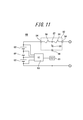
- FIG. 10 shows a protective element 50 as a related technique of the present invention.
- the protective element 50 includes an insulating substrate 51, a heating element 53 laminated on the insulating substrate 51 and covered with an insulating member 52 such as glass, a pair of electrodes 54 and 54 formed on both ends of the insulating substrate 51, A heating element extraction electrode 55 laminated on the member 52 so as to overlap the heating element 53, and a fusible conductor having both ends connected to the pair of electrodes 54, 54 and the center connected to the heating element extraction electrode 55, respectively. 56.
- the heating element extraction electrode 55 is connected to the heating element 53 via the first heating element electrode 57.
- the other end of the heating element 53 is connected to the second heating element electrode 58.
- the protective element 50 is coated with a flux 61 on almost the entire surface of the soluble conductor 56 in order to prevent oxidation of the soluble conductor 56. Further, the protection element 50 may place a cover member on the insulating substrate 51 in order to protect the inside.
- such a protection element 50 is connected to a battery circuit 60 for a lithium ion secondary battery or the like, so that a pair of electrodes 54 and 54 and a soluble conductor 56 are charged to the battery circuit 60. It constitutes a part of the discharge current circuit.
- the second heating element electrode 58 is connected to a current control element such as the FET 61.
- the FET 61 controls the current so that the heating element 53 is energized in response to a signal from a detection circuit 63 that detects an abnormal voltage of the lithium ion battery 62, for example.
- a switch element such as an FET 61 that controls current so as to supply power to the heating element 53 is required, and the battery circuit 60 is configured.
- the manufacturing cost is also disadvantageous.
- an object of the present invention is to provide a protection circuit, a battery circuit, a protection element, and a method for driving the protection element that can be used without using a switching element such as an FET other than the protection element.
- a protection circuit includes a first fusible conductor connected to an external circuit, and a first heating element connected to the first fusible conductor.
- the first heat generating element generates heat
- the first soluble conductor is blown to cut off the external circuit
- a detection circuit is connected to the detection circuit for detecting whether the external circuit is cut off.
- 2 heating elements, a second fusible conductor that melts when the second heating element generates heat, and a switch connected to the first heating element, and by opening the switch A power supply to the first heating element is regulated, and a short-circuit unit that supplies power to the first heating element by short-circuiting the switch by the molten conductor of the second soluble conductor.
- a battery circuit is provided on a battery stack, a detection circuit that detects an abnormal voltage of the battery stack, and a charge / discharge circuit of the battery stack, and the charge / discharge circuit according to a detection result of the detection circuit.
- a protective element for interrupting the discharge circuit comprising: a first soluble conductor connected to the charge / discharge circuit; a first heating element connected to the first soluble conductor; A protection unit that cuts off the charging / discharging circuit when the first fusible conductor is melted when the first heating element generates heat, a second heating element connected to the detection circuit, and A second fusible conductor that melts when the second heating element generates heat; and a switch that is connected to the first heating element. The switch is opened to connect the first heating element to the first heating element. Regulating power supply, the second fusible guide The molten conductor is one having a short circuit portion for supplying power to the first heating element by shorting the switch.
- the protection element according to the present invention is connected to the insulating substrate, the first heating element, the first and second electrodes connected to an external circuit, the first heating element, and the first heating element.
- the first soluble conductor mounted between the first and second electrodes and constituting a part of the external circuit, the second heating element, one end connected to one end of the second heating element, and the other
- a third electrode connected at its end to a detection circuit for detecting whether or not the external circuit needs to be shut off;
- a fourth electrode connected to the other end of the second heating element and the external circuit; Mounted on one or both of the first heating element electrode connected to one heating element, the fourth electrode and the first heating element electrode, and melted by the heat generated by the second heating element, A fourth electrode and a second fusible conductor for short-circuiting the first heating element electrode.
- the protection element driving method is connected to the insulating substrate, the first heating element, the first and second electrodes connected to the external circuit, and the first heating element.
- the first soluble conductor mounted between the first and second electrodes and constituting a part of the external circuit, the second heating element, and one end connected to one end of the second heating element
- a third electrode connected at the other end to a detection circuit for detecting whether the external circuit needs to be shut off, a fourth electrode connected to the other end of the second heating element and the external circuit, Mounted on one or both of the first heating element electrode connected to the first heating element, the fourth electrode and the first heating element electrode, and melted by the heat generated by the second heating element.
- a second soluble conductor that short-circuits between the fourth electrode and the first heating element electrode, and the detection circuit Power is supplied to the second heating element through the third electrode, and the second heating element generates heat to melt the second soluble conductor, and the second soluble conductor.
- the four electrodes and the first heating element electrode are short-circuited by the molten conductor, power is supplied to the first heating element, the first soluble conductor is melted, and the first electrode and the first heating element are blown.
- the power supply to the second heating element is stopped by blocking the gap with the second electrode.
- the power supply to the first heating element of the protection unit can be controlled according to the operation of the short-circuit unit. Therefore, according to the present invention, the current path can be interrupted without using a switching element such as an FET, and the number of parts and the number of assembly steps are not increased.
- FIG. 1A is a plan view showing a protection element to which the present invention is applied.
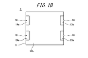
- FIG. 1B is a bottom view showing a protection element to which the present invention is applied.
- FIG. 2 is a circuit diagram showing a protection circuit to which the present invention is applied.
- FIG. 3A is a plan view showing another protective element to which the present invention is applied.
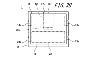
- FIG. 3B is a bottom view showing another protective element to which the present invention is applied.
- FIG. 4A is a plan view showing another protective element to which the present invention is applied.
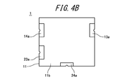
- FIG. 4B is a bottom view showing another protective element to which the present invention is applied.
- FIG. 5A is a plan view showing another protection element to which the present invention is applied.
- FIG. 5B is a bottom view showing another protective element to which the present invention is applied.
- FIG. 6 is a circuit diagram showing another battery circuit to which the present invention is applied.
- FIG. 7 is a circuit diagram showing a battery circuit to which the present invention is applied.
- FIG. 8 is a circuit diagram showing another battery circuit to which the present invention is applied.
- FIG. 9 is a plan view showing another protective element to which the present invention is applied.
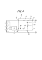
- FIG. 10 is a plan view showing a protection element according to the related art of the present invention.
- FIG. 11 is a circuit diagram showing a battery circuit using a protection element according to the related art of the present invention.
- the protection element 1 to which the present invention is applied is incorporated in an external circuit such as a battery circuit that interrupts the current path by the protection element 1.
- the protective element 1 forms a part of an external circuit on an insulating substrate 11, a protective unit 10 that interrupts the circuit, and a short-circuit unit 20 that configures a switch that operates the protective unit 10. And are formed.
- the protection unit 10 is connected to the first heating element 12, the first and second electrodes 13 and 14 connected to the external circuit, and the first heating element 12, and the first and second electrodes.
- the first fusible conductor 15 is mounted between 13 and 14 and constitutes a part of the external circuit.
- the insulating substrate 11 is formed in a substantially square shape using an insulating member such as alumina, glass ceramics, mullite, zirconia, and the like.
- the insulating substrate 11 may be made of a material used for a printed wiring board such as a glass epoxy board or a phenol board, but the temperature at the time of fusing of the first and second fusible conductors 15 and 26 is noted. There is a need to.
- the first heating element 12 is a conductive member that has a relatively high resistance value and generates heat when energized, and is made of, for example, W, Mo, Ru, or the like.
- the first heating element 12 has one end connected to the first heating element electrode 25 formed in the short-circuit portion 20 and the other end connected to the heating element extraction electrode 17 connected to the first soluble conductor 15. ing.
- the first heating element 12 is covered with an insulating layer 16 on the surface 11 a of the insulating substrate 11.
- the insulating layer 16 is provided to protect and insulate the first heating element 12, and to efficiently transmit the heat of the first heating element 12 to the first soluble conductor 15 and the heating element extraction electrode 17, For example, it consists of a glass layer.
- an insulating layer 16 is also formed between the surface 11a of the insulating substrate 11 and the first heating element 12, and the first heating element 12 is disposed inside the insulating layer 16. Also good.
- a heating element extraction electrode 17 connected to the first heating element 12 is laminated on the upper surface of the insulating layer 16.
- the heating element extraction electrode 17 can be made to easily aggregate the molten conductor of the first soluble conductor 15 by being heated by the first heating element 12.
- a first electrode 13 and a second electrode 14 are formed on a pair of left and right side edges of the insulating substrate 11.
- the first soluble conductor 15 is mounted on the first and second electrodes 13 and 14 via mounting solder.
- the first and second electrodes 13 and 14 face the side surface of the insulating substrate 11, and as shown in FIG. 1B, the first and second electrodes provided on the back surface 11b of the insulating substrate 11 through the through holes 18, respectively.
- the external connection electrodes 13a and 14a are connected.
- the first and second electrodes 13 and 14 are connected to an external circuit of a device on which the protection element 1 is mounted via the first and second external connection electrodes 13a and 14a.
- the first and second electrodes 13 and 14 can be formed using a general electrode material such as Cu or Ag.
- a coating such as Ni / Au plating, Ni / Pd plating, or Ni / Pd / Au plating is formed on the surfaces of the first and second electrodes 13 and 14 by a known plating process. preferable. Thereby, the oxidation of the 1st, 2nd electrodes 13 and 14 can be prevented, and a molten conductor can be hold
- the mounting solder connecting the first fusible conductor 15 or the low melting point metal forming the outer layer of the first fusible conductor 15 melts the first and first It is possible to prevent the two electrodes 13 and 14 from being eroded (soldered).
- any metal that can be melted quickly by the heat generated by the first heating element 12 can be used.
- a low melting point metal such as Pb-free solder mainly containing Sn is suitable. Can be used.
- the first soluble conductor 15 may be formed by laminating a low melting point metal and a high melting point metal.
- a laminated structure of a low-melting-point metal and a high-melting-point metal for example, a structure in which a low-melting-point metal foil is coated with a high-melting-point metal plating can be exemplified.
- solder such as Pb-free solder containing Sn as a main component
- the high melting point metal it is preferable to use Ag, Cu or an alloy containing these as main components.
- the protective element 1 when the protective element 1 is reflow mounted, even if the reflow temperature exceeds the melting temperature of the low melting point metal and the low melting point metal melts, Outflow to the outside can be suppressed and the shape of the first soluble conductor 15 can be maintained. In addition, even when fusing, the low melting point metal melts, and the high melting point metal is eroded (soldered), so that the fusing can be quickly performed at a temperature lower than the melting point of the high melting point metal.
- the first soluble conductor 15 may be provided with a flux in order to prevent oxidation and improve wettability at the time of melting.
- the first fusible conductor 15 is mounted between the first and second electrodes 13 and 14 connected to the external circuit, and is connected to the heating element extraction electrode 17 stacked on the insulating layer 16.
- the first fusible conductor 15 is melted between the first electrode 13 and the second electrode 14 due to the heat generated by the first heating element 12, thereby blocking the current path of the external circuit. it can.
- the short-circuit portion 20 functions as a switch that controls power supply to the first heating element 12.
- the short-circuit unit 20 has a third heating element 22 connected to the second heating element 22, one end connected to one end of the second heating element 22, and the other end connected to the detection circuit 3 that detects whether or not the external circuit needs to be blocked.
- a molten conductor 26 is melted by the heat generated by the second heating element 22, and short-circuits between the fourth electrode 24 and the first heating element electrode 25.
- a molten conductor 26 is melted by the heat generated by the second heating element 22, and short-circuits between the fourth electrode 24 and the first
- the second heating element 22 can be formed by the same material and the same process as the first heating element 12 described above.
- the second heating element 22 has one end connected to the third electrode 23 and the other end connected to the fourth electrode 24.
- the second heating element 22 is also covered with the insulating layer 16 on the surface 11 a of the insulating substrate 11. Further, the second heating element 22 may also be disposed inside the insulating layer 16 formed on the surface 11 a of the insulating substrate 11.
- the third electrode 23 and the fourth electrode 24 are formed on a pair of left and right side edges of the insulating substrate 11 in FIG. 1A.
- the third and fourth electrodes 23 and 24 face the side surface of the insulating substrate 11, and as shown in FIG. 1B, the third and fourth electrodes provided on the back surface 11b of the insulating substrate 11 through the through holes 18.
- the 3rd electrode 23 is connected with the detection circuit 3 which detects the necessity of interruption
- the fourth electrode 24 is connected to the current path of the external circuit via the fourth external connection electrode 24a.
- the fourth electrode 24 and the first heating element electrode 25 are laminated on the insulating layer 16 covering the second heating element 22.
- the fourth electrode 24 and the first heating element electrode 25 are opened by being separated by a predetermined distance.
- a second soluble conductor 26 is mounted on one or both of the fourth electrode 24 and the first heating element electrode 25 via mounting solder, and the second heating element 22 generates heat to generate a second.
- the fusible conductor 26 is melted, the molten conductor is agglomerated and bonded so that a short circuit is possible.
- the first heating element electrode 25 is connected to one end of the first heating element 12 of the protection unit 10 and short-circuited with the fourth electrode 24, whereby the first soluble conductor 15 to the first soluble conductor 15, A power supply path to the first heating element 12 that reaches the fourth electrode 24 through the heating element extraction electrode 17, the first heating element 12, and the first heating element electrode 25 is formed.
- the third and fourth electrodes 23 and 24 and the first heating element electrode 26 can be formed using a general electrode material such as Cu or Ag.
- a coating such as Ni / Au plating, Ni / Pd plating, Ni / Pd / Au plating, etc. is used. It is preferably formed by treatment.
- the fourth electrode 24 and the first heating element electrode 25 are normally opened, and the power supply to the first heating element 12 is restricted.
- the detection circuit 3 detects that the external circuit needs to be interrupted, the short circuit unit 20 is supplied with current from the detection circuit 3 to the third electrode 23, the second heating element 22 generates heat, Two soluble conductors 26 are melted.
- the fourth electrode 24 and the first heating element electrode 25 are short-circuited via the molten conductor of the second soluble conductor 26, and power is supplied to the first heating element 12. It becomes like this.
- the second soluble conductor 26 can be formed of the same material and the same configuration as the first soluble conductor 15 described above.
- the inside of the protection element 1 is protected by covering the surface 11a side of the insulating substrate 11 with a cover member (not shown).
- the cover member is formed using an insulating member such as a thermoplastic plastic, a ceramic, a glass epoxy substrate, and the like, similarly to the insulating substrate 11.
- the protection circuit 30 includes the first and second electrodes 13 and 14 of the protection unit 10 connected via the first fusible conductor 15 and the first heating element 12. One end is connected to the first electrode 13 via the first soluble conductor 15, and the other end is connected to the first heating element electrode 25. Further, in the protection circuit 30, the third and fourth electrodes 23 and 24 of the short-circuit portion 20 are continuous via the second heating element 22. Further, the protection circuit 30 includes a switch 21 that is short-circuited when the fourth electrode 24 and the first heating element electrode 25 of the short-circuit portion 20 are opened in the initial state and the second soluble conductor 26 is melted. Configure.
- the protection circuit 30 is connected in series on the current path of the circuit board on which the protection element 1 is mounted, so that the first and second electrodes 13 and 14 of the protection unit 10 are connected to a power supply circuit, a digital signal circuit, or the like. It is incorporated between the main external circuits 2A and 2B and constitutes a part of the current path of the external circuits 2A and 2B.
- the protection circuit 30 is connected via the third electrode 23 to the detection circuit 3 that detects whether or not the external circuits 2A and 2B need to be blocked.
- the detection circuit 3 is a circuit that detects whether it is necessary to cut off between the various external circuits 2A and 2B in which the protective element 1 is incorporated. For example, the charge / discharge current circuit is cut off when the battery pack has an abnormal voltage, network communication Current path between the external circuits 2A and 2B physically and irreversibly by the protection unit 10, such as interruption of the digital signal circuit connected to the data server for hacking or cracking in the device, or expiration of the license period of the device or software When it is necessary to shut off, the short-circuit unit 20 is operated.
- the second heating element 22 generates heat, so that the second soluble conductor 26 is first melted.
- the molten conductor of the second soluble conductor 26 is attracted onto the fourth electrode and the first heating element electrode 25 having high wettability and a large area, and the molten conductor aggregated on the fourth electrode 24;
- the molten conductor aggregated on the first heating element electrode 25 is bonded.
- the fourth electrode 24 and the first heating element electrode 25 are short-circuited via the molten conductor, and the fourth electrode 24 and the first heating element are interposed via the molten conductor of the second soluble conductor 26.
- the electrode 25 is short-circuited, and reaches the first soluble conductor 15, the heating element extraction electrode 17, the first heating element 12, the first heating element electrode 25, and the fourth electrode 24 from the first electrode 13.
- a power supply path to one heating element 12 is formed.
- the protection element 1 when the first heating element 12 is energized and generates heat, the first soluble conductor 15 is fused. Since the molten conductor of the first soluble conductor 15 aggregates on the heating element extraction electrode 17 and the first and second electrodes 13 and 14, the space between the first and second electrodes 13 and 14 is opened. As a result, the protection element 1 physically and irreversibly blocks the current path between the external circuits 2A and 2B.
- the protection element 1 since the power supply to the second heating element 22 is stopped by the detection circuit 3 that detects that the current path between the external circuits 2A and 2B is interrupted, the protection element 1 has the second heating element 22. The fever is stopped. Detection of interruption of the current path between the external circuits 2A and 2B by the detection circuit 3 is performed, for example, by measuring the voltages of the external circuits 2A and 2B.
- the detection circuit 3 includes a timer that sets a necessary and sufficient predetermined time from the start of power supply to the second heating element 22 to the fusing of the first soluble conductor 15 by the first heating element 15. You may stop the electric power feeding to the 2nd heat generating body 22 after the said predetermined time progress.
- the power supply to the first heating element 12 of the protection unit 10 can be controlled according to the operation of the short-circuit unit 20. Therefore, according to the protection element 1 and the protection circuit 30, the current path can be interrupted without using a switching element such as an FET, and the number of parts and the number of assembling steps are not increased.
- the protection unit 10 can be shut off stably and reliably.
- the first and second heating elements 12 and 22 are formed on the surface 11a of the insulating substrate 11, and the first and second soluble conductors 15 and 26 are superimposed.
- the first and second heating elements 12 and 22 may be formed on the back surface 11b of the insulating substrate 11 as shown in FIGS. 3A and 3B. In this case, the first and second heating elements 12 and 22 are covered with the insulating layer 16 on the back surface 11 b of the insulating substrate 11.
- the heating element extraction electrode 17 connected to one end of the first heating element 12 is provided on the front surface 11a, the front surface portion 17a connected to the first fusible conductor 15, and the first surface provided on the back surface 11b.
- the heat generating body 12 has a back surface portion 17 b connected to one end thereof, and the front surface portion 17 a and the back surface portion 17 b are connected via the conductive through hole 18.
- the first heating element electrode 25 is also formed on the surface 11a of the insulating substrate 11 and is short-circuited with the fourth electrode 24 via the molten conductor of the second soluble conductor 26, and the back surface. 11 b and a back surface portion 25 b connected to one end of the first heating element 12, and the front surface portion 25 a and the back surface portion 25 b are connected via the conductive through hole 18.
- the third and fourth electrodes 23 and 24 are formed with the second heating element 22 between the third and fourth external connection electrodes 23a and 24a formed on the back surface 11b of the insulating substrate 11. Yes. Moreover, it is preferable that the 1st, 2nd heat generating bodies 12 and 22 are formed in the back surface 11b of the insulated substrate 11 in the position which overlaps with the 1st and 2nd soluble conductors 15 and 26, respectively.
- the surface 11a of the insulating substrate 11 is flattened by forming the first and second heating elements 12, 22 on the back surface 11b of the insulating substrate 11.
- the protective element 1 allows the first to fourth electrodes 13, 14, 23, 24, the surface portion 17a of the heating element extraction electrode 17, and the surface portion 25a of the first heating element electrode 25 to be flat surfaces. 11a can be formed. Therefore, the protective element 1 can simplify the manufacturing process of each of these electrodes 13, 14, 23, 24, 17, 25, and can reduce the height.
- the protective element 1 is made of a material having excellent thermal conductivity such as fine ceramic as the material of the insulating substrate 11 even when the first and second heating elements 12 and 22 are formed on the back surface 11b of the insulating substrate 11.
- the first and second soluble conductors 15 and 26 can be heated and melted in the same manner as when the first and second heating elements 12 and 22 are stacked on the surface 11a of the insulating substrate 11. .
- the protective element 1 includes the first and second fusible conductors 15 and 26 on the surface 11a of the insulating substrate 11 with the first and second heating elements 12 and 22 disposed thereon. May be formed side by side. In this case, the first and second heating elements 12 and 22 are covered with the insulating layer 16. In this case, the heating element extraction electrode 17 and the first heating element electrode 25 connected to the first heating element 12 are formed as a single layer on the surface 11 a of the insulating substrate 11. The third and fourth electrodes 23 and 24 connected to the second heating element 22 are also formed as a single layer on the surface 11 a of the insulating substrate 11.
- the protection element 1 may form the first and second heating elements 12 and 22 inside the insulating substrate 11. In this case, it is not necessary to provide the insulating layer 16 that covers the heating element 17. Moreover, it is preferable that the 1st, 2nd heat generating bodies 12 and 22 are formed in the inside of the insulated substrate 11 in the position which overlaps with the 1st and 2nd soluble conductors 15 and 26, respectively.
- the protection element 1 and the protection circuit 30 are provided with a third fusible conductor 27 on the power supply path to the second heating element 22, and the switch 21 After the short circuit, the third soluble conductor 27 may be blown by the heat generated by the second heating element 22 before the first soluble conductor 15 is blown.
- the protection element 1 and the protection circuit 30 automatically short-circuit the switch 21 to form a power feeding path to the first heating element 12 and then automatically blow the second soluble conductor 27 to blow the second.
- the power supply path to the heat generating element 22 can be cut off, and the heat generation of the second heat generating element 22 can be stopped. Accordingly, in the protection element 1 and the protection circuit 30, the current flowing through the first heating element 12 flows into the detection circuit 3 side via the second heating element 22 and the third electrode 23. Can be prevented.
- the protection element 1 is provided with a second heating element electrode 28 between the fourth electrode 24 and the other end of the second heating element 22.
- the second heating element electrode 28 is connected to the other end of the second heating element 22.
- fever of the 2nd heat generating body 22 is mounted. That is, the fourth electrode 24 is connected to the second heating element 22 through the third soluble conductor 27 and the second heating element electrode 28.
- the third soluble conductor 27 can be formed of the same material and configuration as the first and second soluble conductors 15 and 26 described above.
- the protection element 1 when the second heating element 22 generates heat, the second soluble conductor 26 is first melted, and the fourth electrode 24 and the first heating element electrode 25 are short-circuited. As a result, a power supply path to the first heating element 12 that reaches the second electrode 14, the first soluble conductor 15, the heating element extraction electrode 17, the first heating element electrode 25, and the fourth electrode 24 is formed. To do.
- the protective element 1 blocks the power supply path from the third electrode 23 to the second electrode 24 through the second heater 22 to the fourth electrode 24, so that the second heater 22 Heat generation can be stopped automatically.
- the 4th electrode 24, the 2nd heat generating body 22, and the 3rd electrode are interrupted
- the protection element 1 is formed so that the second soluble conductor 26 is melted before the third soluble conductor 27 is melted. If the third soluble conductor 27 is melted before the second soluble conductor 26 is melted, the power supply to the second heating element 22 is stopped, the second soluble conductor 26 is not melted, This is because a power supply path to one heating element 12 cannot be formed.
- the protection element 1 is formed so that the second soluble conductor 26 is melted first when the second heating element 22 generates heat. Specifically, the second soluble conductor 26 of the protection element 1 is mounted at a position closer to the heat generation center of the second heating element 22 than the third soluble conductor 27.
- the heat generation center of the second heat generating element 22 refers to a region where the temperature becomes the highest in the initial stage of heat generation in the heat distribution that is generated when the second heat generating element 22 generates heat.
- the heat generated from the second heating element 22 has the largest amount of heat released from the insulating substrate 11, and when the insulating substrate 11 is formed of a ceramic material having excellent thermal shock resistance but high thermal conductivity, insulation is performed. Heat diffuses to the substrate 11. Therefore, in the initial stage of heat generation when energization is started, the center of the second heating element 22 that is farthest from the outer edge in contact with the insulating substrate 11 is the hottest, and the heat is dissipated toward the outer edge in contact with the insulating substrate 11, so that the temperature is unlikely to rise. Become.
- the protection element 1 includes the second fusible conductor 26 that has the highest heat generation center C at the initial heating stage of the second heating element 22 than the third fusible conductor 27.
- the third soluble conductor 27 is heated later than the second soluble conductor 26, the third soluble conductor 27 is blown after the second soluble conductor 26 is melted.
- the protective element 1 is preferably formed such that the third soluble conductor 27 is blown before the first soluble conductor 15.
- the short-circuit part 20 is a switch for operating the protection part 10, and immediately stops the heat generation of the second heating element 22 after the feeding path to the first heating element 12 is formed. It is preferable to do.
- the protection element 1 has the third electrode 23 via the fourth electrode 24 on the power supply path to the first heating element 12. It is preferable to prevent the feeding current to the first heating element 12 from flowing into the side.
- the protection element 1 is formed such that when the second heating element 22 generates heat, the third soluble conductor 27 is blown first.
- the protection element 1 changes the shapes of the first soluble conductor 15 and the third soluble conductor 27 so that the third soluble conductor 27 comes before the first soluble conductor 15. You may make it melt.
- the first soluble conductor 15 can be blown out before the first soluble conductor 15.
- the thickness of the high melting point metal layer is set to the third fusible conductor 27.
- the first soluble conductor 15 may be thin and may be thick, or the low melting point metal foil may be thin in the third soluble conductor 27 and thick in the first soluble conductor 15.
- the protection element 1 may be formed so that the width direction orthogonal to the current direction of the third soluble conductor 27 is narrower than the width direction orthogonal to the current direction of the first soluble conductor 15.
- the protective element 1 can change the melting point by changing the layer structure, for example, the third soluble conductor 27 is formed of a low melting point metal and the first soluble conductor 15 is formed of a high melting point metal. And relatively facilitating fusing of the third fusible conductor 27 than the first fusible conductor 15, and causing the third fusible conductor 27 to blow out before the first fusible conductor 15. May be.
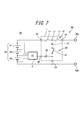
- FIG. 7 shows a configuration of a battery circuit 40 as an example of an external circuit to which the protection circuit is applied.
- the battery circuit 40 is, for example, a circuit in a battery pack 50 of a lithium ion secondary battery, and is charged when a battery stack 45 including three lithium ion secondary battery battery cells 41 to 43 and the battery stack 45 is abnormal.
- the protection element 1 to which the present invention is applied and the detection circuit 3 for detecting the voltage of each of the battery cells 41 to 43 are provided.
- the battery stack 45 is formed by connecting battery cells 41 to 43 that need to be controlled for protection from overcharge and overdischarge states, and is detachable via the positive terminal 50a and the negative terminal 50b of the battery pack 50. And a charging voltage from the charging device is applied.
- the battery pack 50 charged by the charging device can operate the electronic device by connecting the positive terminal 50a and the negative terminal 50b to the electronic device operating with the battery.
- the protection element 1 includes, for example, the first and second electrodes 13 and 14 of the protection unit 10 connected in series on the charge / discharge current path on the positive electrode side of the battery stack 45, and the third electrode 23 of the short-circuit unit 20 Connected to the detection circuit 3, the fourth electrode 24 is connected to the charge / discharge current path on the negative electrode side of the battery stack 45.
- the detection circuit 3 is connected to each of the battery cells 41 to 43 and detects the voltage value of each of the battery cells 41 to 43.
- the detection circuit 3 is connected to the third electrode 23 of the protection element 1, and the short circuit portion 20 of the protection element 1 is connected when any one of the battery cells 41 to 43 becomes an overcharge voltage or an overdischarge voltage. Outputs the control signal to be activated.
- the second heating element 22 generates heat by the electric power output from the detection circuit 3, and the second soluble conductor 26 is melted.
- the fourth electrode 24 and the first heating element electrode 25 are short-circuited, the switch 21 is turned on, and the first heating element 12 from the first electrode 13 to the fourth electrode 24 is turned on.
- a power supply path to is formed.
- the first heating element 12 generates heat in the protection element 1, the first soluble conductor 15 is melted and the charge / discharge current path of the battery stack 45 can be blocked.
- the short circuit portion 20 of the protection element 1 causes the switch 21 to be in an off state in normal times, thereby restricting the power supply to the first heating element 12 of the protection portion 10, and the detection circuit 3
- the battery circuit 40 does not need to be provided with a switch element such as an FET for operating the protection element 1 in addition to the protection element 1, and does not increase the number of parts and the number of assembly steps.
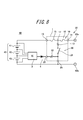
- the battery circuit 40 may be provided with a rectifying element 4 between the detection circuit 3 and the second heating element 22 to prevent current from flowing into the detection circuit 3.
- the rectifying element 4 allows current to flow from the detection circuit 3 to the protection element 1 side, but does not cause current to flow from the protection element 1 to the detection circuit 3 side.
- the battery circuit 40 allows the fourth electrode 24, the second heating element 22, and the third electrode when the power supply path to the first heating element 12 is formed. Thus, it is possible to prevent the current supplied to the first heating element 12 from flowing into the detection circuit 3 through the control circuit 23.
- the battery circuit 40 includes the third fusible conductor 27 between the fourth electrode 24 and the second heating element 22 of the protection element 1 as described above, and supplies power to the first heating element 12. It is also possible to prevent the feeding current to the first heating element 12 from flowing into the detection circuit 3 by fusing the third soluble conductor 27 after forming the path.
- the protection element 1 of the present invention is not limited to use in a battery pack of a lithium ion secondary battery, and can of course be applied to various uses that require interruption of a current path by an electric signal.
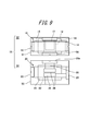
- the protection part 10 and the short-circuit part 20 are formed on the insulating substrate 11 and formed into one chip.
- the protection element according to the present invention separates the protection part 10 and the short-circuit part 20 from each other. It may be formed by two chips to be provided and connected. That is, as shown in FIG. 9, the protective member 52 having the protective part 10 formed on the insulating substrate 51 and the shorting member 54 having the short-circuit part 20 formed on the insulating substrate 53 are provided. And the short-circuit member 54 may be connected to form the protective element 55.
- An external connection electrode 56 connected to the first heating element 12 is formed on the protective member 52. Further, the external connection electrode 25 a is also formed on the first heating element electrode 25 on the short-circuit member 54.
- the protective element 55 is connected to the first heating element electrode 25 and the first heating element 12 by connecting the external connection electrodes 56 and 25a. These external connection electrodes 56 and 25a can be connected by, for example, mounting the protective member 52 and the short-circuit member 54 on a circuit board of an external circuit on which the protective element 55 is mounted.
- SYMBOLS 1 Protection element 2A, 2B external circuit, 3 detection circuit, 10 protection part, 11 insulation board, 11a surface, 11b back surface, 12 1st heat generating body, 13 1st electrode, 13a 1st external connection electrode, 14 2nd electrode, 14a 2nd external connection electrode, 15 1st soluble conductor, 16 insulation layer, 17 heating element extraction electrode, 18 through hole, 20 short circuit part, 21 switch, 22 2nd heating element, 23 Third electrode, 23a, third external connection electrode, 24, fourth electrode, 24a, fourth external connection electrode, 25, first heating element electrode, 26, second soluble conductor, 27, third soluble conductor , 28 2nd heating element electrode, 30 protection circuit, 40 battery circuit, 41-43 battery cell, 45 battery stack, 50 battery pack
Landscapes
- Chemical & Material Sciences (AREA)
- Chemical Kinetics & Catalysis (AREA)
- Electrochemistry (AREA)
- General Chemical & Material Sciences (AREA)
- Engineering & Computer Science (AREA)
- Combustion & Propulsion (AREA)
- Fuses (AREA)
- Connection Of Batteries Or Terminals (AREA)
Abstract
FET等のスイッチ素子を用いることなく使用できる保護回路を提供する。 外部回路(2A,2B)に接続された第1の可溶導体(15)と、第1の可溶導体(15)と接続された第1の発熱体(12)とを備え、第1の発熱体(12)が発熱することにより第1の可溶導体(15)が溶断し外部回路(2A,2B)を遮断する保護部(10)と、外部回路(2A,2B)の遮断の要否を検出する検出回路(3)と接続された第2の発熱体(22)と、第2の発熱体(22)が発熱することにより溶融する第2の可溶導体と、第1の発熱体(12)と接続されたスイッチ(21)とを備え、スイッチ(21)を開放させることにより第1の発熱体(12)への給電を規制し、第2の可溶導体(22)の溶融導体によってスイッチ(21)を短絡させることにより第1の発熱体(12)へ電力を供給する短絡部(20)とを有する。
Description
本出願は、日本国特許出願2013-228747号(2013年11月1日出願)の優先権を主張するものであり、当該出願の開示全体を、ここに参照のために取り込む。
本発明は、電流経路を遮断する保護素子に関し、特にリチウムイオンバッテリ等の緊急時に速やかに電流経路を遮断する必要のある回路に用いて好適な保護回路、バッテリ回路、保護素子、及び保護素子の駆動方法に関する。
充電して繰り返し利用することのできる二次電池の多くは、バッテリパックに加工されてユーザに提供される。特に重量エネルギー密度の高いリチウムイオン二次電池においては、ユーザ及び電子機器の安全を確保するために、一般的に、過充電保護、過放電保護等のいくつもの保護回路をバッテリパックに内蔵し、所定の場合にバッテリパックの出力を遮断する機能を有している。
この種の保護回路では、バッテリパックに内蔵されたFETスイッチを用いて出力のON/OFFを行うことにより、バッテリパックの過充電保護又は過放電保護動作を行う。しかしながら、何らかの原因でFETスイッチが短絡破壊した場合、雷サージ等が印加されて瞬間的な大電流が流れた場合、あるいはバッテリセルの寿命によって出力電圧が異常に低下したり、逆に過大異常電圧を出力した場合であっても、バッテリパックや電子機器は、発火等の事故から保護されなければならない。そこで、このような想定し得るいかなる異常状態においても、バッテリセルの出力を安全に遮断するために、外部からの信号によって電流経路を遮断する機能を有するヒューズ素子からなる保護素子が用いられる。
このようなリチウムイオン二次電池等向けの保護回路の保護素子として、保護素子内部に発熱体を有し、この発熱体によって電流経路上の可溶導体を溶断する構造が一般的に用いられている。
本発明の関連技術として、図10に保護素子50を示す。保護素子50は、絶縁基板51と、絶縁基板51に積層され、ガラス等の絶縁部材52に覆われた発熱体53と、絶縁基板51の両端に形成された一対の電極54,54と、絶縁部材52上に発熱体53と重畳するように積層された発熱体引出電極55と、両端が一対の電極54,54にそれぞれ接続され、中央部が発熱体引出電極55に接続された可溶導体56とを備える。
発熱体引出電極55の一端は、第1の発熱体電極57を介して発熱体53に接続される。また、発熱体53の他端は、第2の発熱体電極58に接続される。なお、保護素子50は、可溶導体56の酸化防止のために、可溶導体56上のほぼ全面にフラックス61が塗布されている。また、保護素子50は、内部を保護するためにカバー部材を絶縁基板51上に載置してもよい。
このような保護素子50は、図11に示すように、リチウムイオン二次電池等向けバッテリ回路60に接続されることにより、一対の電極54,54及び可溶導体56が当該バッテリ回路60の充放電電流回路の一部を構成する。また、保護素子50は、第2の発熱体電極58がFET61等の電流制御素子に接続される。FET61は、例えばリチウムイオンバッテリ62の異常電圧を検出する検出回路63からの信号に応じて発熱体53が通電されるように電流を制御する。
このような保護素子50、及びバッテリ回路60では、保護素子50に加え、発熱体53に対して電力を供給するように電流を制御するFET61等のスイッチ素子が必要となり、バッテリ回路60を構成する部品点数の増加や、組み立て工数の増加を招く他、製造コスト上も不利となる。
そこで、本発明は、保護素子の他にFET等のスイッチ素子を用いることなく使用することができる保護回路、バッテリ回路、保護素子、及び保護素子の駆動方法を提供することを目的とする。
上述した課題を解決するために、本発明に係る保護回路は、外部回路に接続された第1の可溶導体と、上記第1の可溶導体と接続された第1の発熱体とを備え、上記第1の発熱体が発熱することにより上記第1の可溶導体が溶断し上記外部回路を遮断する保護部と、上記外部回路の遮断の要否を検出する検出回路と接続された第2の発熱体と、上記第2の発熱体が発熱することにより溶融する第2の可溶導体と、上記第1の発熱体と接続されたスイッチとを備え、上記スイッチを開放させることにより上記第1の発熱体への給電を規制し、上記第2の可溶導体の溶融導体によって上記スイッチを短絡させることにより上記第1の発熱体へ電力を供給する短絡部とを有するものである。
また、本発明に係るバッテリ回路は、バッテリスタックと、上記バッテリスタックの異常電圧を検出する検出回路と、上記バッテリスタックの充放電回路上に設けられ、上記検出回路の検出結果に応じて上記充放電回路を遮断する保護素子とを有し、上記保護素子は、上記充放電回路に接続された第1の可溶導体と、上記第1の可溶導体と接続された第1の発熱体とを備え、上記第1の発熱体が発熱することにより上記第1の可溶導体が溶断し上記充放電回路を遮断する保護部と、上記検出回路と接続された第2の発熱体と、上記第2の発熱体が発熱することにより溶融する第2の可溶導体と、上記第1の発熱体と接続されたスイッチとを備え、上記スイッチを開放させることにより上記第1の発熱体への給電を規制し、上記第2の可溶導体の溶融導体によって上記スイッチを短絡させることにより上記第1の発熱体へ電力を供給する短絡部とを有するものである。
また、本発明に係る保護素子は、絶縁基板と、第1の発熱体と、外部回路に接続された第1、第2の電極と、上記第1の発熱体と接続されるとともに、上記第1、第2の電極間にわたって搭載され、上記外部回路の一部を構成する第1の可溶導体と、第2の発熱体と、一端を上記第2の発熱体の一端と接続され、他端を上記外部回路の遮断の要否を検出する検出回路と接続された第3の電極と、上記第2の発熱体の他端及び上記外部回路と接続された第4の電極と、上記第1の発熱体と接続された第1の発熱体電極と、上記第4の電極及び上記第1の発熱体電極の一方又は両方に搭載され、上記第2の発熱体の発熱により溶融し、上記第4の電極及び上記第1の発熱体電極間を短絡させる第2の可溶導体とを有するものである。
また、本発明に係る保護素子の駆動方法は、絶縁基板と、第1の発熱体と、外部回路に接続された第1、第2の電極と、上記第1の発熱体と接続されるとともに、上記第1、第2の電極間にわたって搭載され、上記外部回路の一部を構成する第1の可溶導体と、第2の発熱体と、一端を上記第2の発熱体の一端と接続され、他端を上記外部回路の遮断の要否を検出する検出回路と接続された第3の電極と、上記第2の発熱体の他端及び上記外部回路と接続された第4の電極と、上記第1の発熱体と接続された第1の発熱体電極と、上記第4の電極及び上記第1の発熱体電極の一方又は両方に搭載され、上記第2の発熱体の発熱により溶融し、上記第4の電極及び上記第1の発熱体電極間を短絡させる第2の可溶導体とを有し、上記検出回路から上記第3の電極を介して上記第2の発熱体に電力を供給し、上記第2の発熱体が発熱することにより上記第2の可溶導体を溶融させ、上記第2の可溶導体の溶融導体により上記4の電極及び上記第1の発熱体電極を短絡させ、上記第1の発熱体に電力が供給され、上記第1の可溶導体が溶断し、上記第1の電極と上記第2の電極との間を遮断し、上記第2の発熱体に対する給電を停止するものである。
本発明によれば、短絡部の動作に応じて、保護部の第1の発熱体への給電を制御することができる。したがって、本発明によれば、FET等のスイッチ素子を用いることなく、電流経路の遮断を行うことができ、部品点数の増加や、組み立て工数の増加を招くこともない。
以下、本発明が適用された保護回路、バッテリ回路、保護素子、保護素子の駆動方法について、図面を参照しながら詳細に説明する。なお、本発明は、以下の実施形態のみに限定されるものではなく、本発明の要旨を逸脱しない範囲内において種々の変更が可能であることは勿論である。また、図面は模式的なものであり、各寸法の比率等は現実のものとは異なることがある。具体的な寸法等は以下の説明を参酌して判断すべきものである。また、図面相互間においても互いの寸法の関係や比率が異なる部分が含まれていることは勿論である。
[保護素子]
本発明が適用された保護素子1は、例えばバッテリ回路等の、保護素子1によってその電流経路を遮断する外部回路に組み込まれる。保護素子1は、図1Aに示すように、絶縁基板11上に、外部回路の一部を構成し、当該回路を遮断する保護部10と、保護部10を作動させるスイッチを構成する短絡部20とが形成されている。
本発明が適用された保護素子1は、例えばバッテリ回路等の、保護素子1によってその電流経路を遮断する外部回路に組み込まれる。保護素子1は、図1Aに示すように、絶縁基板11上に、外部回路の一部を構成し、当該回路を遮断する保護部10と、保護部10を作動させるスイッチを構成する短絡部20とが形成されている。
[保護部]
保護部10は、第1の発熱体12と、外部回路に接続された第1、第2の電極13,14と、第1の発熱体12と接続されるとともに、第1、第2の電極13,14間にわたって搭載され、外部回路の一部を構成する第1の可溶導体15を有する。
保護部10は、第1の発熱体12と、外部回路に接続された第1、第2の電極13,14と、第1の発熱体12と接続されるとともに、第1、第2の電極13,14間にわたって搭載され、外部回路の一部を構成する第1の可溶導体15を有する。
絶縁基板11は、たとえば、アルミナ、ガラスセラミックス、ムライト、ジルコニアなどの絶縁性を有する部材を用いて略方形状に形成されている。絶縁基板11は、その他にも、ガラスエポキシ基板、フェノール基板等のプリント配線基板に用いられる材料を用いてもよいが、第1、第2の可溶導体15,26の溶断時の温度に留意する必要がある。
第1の発熱体12は、比較的抵抗値が高く通電すると発熱する導電性を有する部材であって、たとえばW、Mo、Ru等からなる。これらの合金あるいは組成物、化合物の粉状体を樹脂バインダ等と混合して、ペースト状にしたものを絶縁基板11の表面11a上にスクリーン印刷技術を用いてパターン形成して、焼成する等によって形成する。
第1の発熱体12は、一端が短絡部20に形成された第1の発熱体電極25と接続され、他端が第1の可溶導体15と接続される発熱体引出電極17と接続されている。第1の発熱体12は、絶縁基板11の表面11a上において絶縁層16に被覆されている。絶縁層16は、第1の発熱体12の保護及び絶縁を図るとともに、第1の発熱体12の熱を効率よく第1の可溶導体15及び発熱体引出電極17へ伝えるために設けられ、例えばガラス層からなる。なお、保護素子1は、絶縁基板11の表面11aと第1の発熱体12との間にも絶縁層16を形成し、第1の発熱体12を絶縁層16の内部に配置するようにしてもよい。
絶縁層16の上面には、第1の発熱体12と接続された発熱体引出電極17が積層されている。発熱体引出電極17は、第1の発熱体12によって加熱されることにより、第1の可溶導体15の溶融導体を凝集しやすくすることができる。
図1A中、絶縁基板11の左右一対の側縁部には、第1の電極13及び第2の電極14が形成されている。第1、第2の電極13,14は、実装用ハンダを介して、第1の可溶導体15が搭載されている。また、第1、第2の電極13,14は、絶縁基板11の側面に臨み、図1Bに示すように、スルーホール18を介して絶縁基板11の裏面11bに設けられた第1、第2の外部接続電極13a,14aと接続されている。そして、第1、第2の電極13,14は、第1、第2の外部接続電極13a,14aを介して、保護素子1が実装されるデバイスの外部回路と接続される。
これら第1、第2の電極13,14は、CuやAg等の一般的な電極材料を用いて形成することができる。また、第1、第2の電極13,14の表面上には、Ni/Auメッキ、Ni/Pdメッキ、Ni/Pd/Auメッキ等の被膜が、公知のメッキ処理により形成されていることが好ましい。これにより、第1、第2の電極13,14の酸化を防止し、溶融導体を確実に保持させることができる。また、保護素子1をリフロー実装する場合に、第1の可溶導体15を接続する実装用ハンダあるいは第1の可溶導体15の外層を形成する低融点金属が溶融することにより第1、第2の電極13,14を溶食(ハンダ食われ)するのを防ぐことができる。
第1の可溶導体15は、第1の発熱体12の発熱により速やかに溶断されるいずれの金属を用いることができ、例えば、Snを主成分とするPbフリーハンダ等の低融点金属を好適に用いることができる。
また、第1の可溶導体15は、低融点金属と高融点金属とを積層して形成してもよい。低融点金属と高融点金属との積層構造としては、例えば、低融点金属箔を高融点金属メッキによって被覆する構造を挙げることができる。低融点金属としては、Snを主成分とするPbフリーハンダなどのハンダを用いることが好ましく、高融点金属としては、Ag、Cu又はこれらを主成分とする合金などを用いることが好ましい。高融点金属と低融点金属とを含有することによって、保護素子1をリフロー実装する場合に、リフロー温度が低融点金属の溶融温度を超えて、低融点金属が溶融しても、低融点金属の外部への流出を抑制し、第1の可溶導体15の形状を維持することができる。また、溶断時も、低融点金属が溶融することにより、高融点金属を溶食(ハンダ食われ)することで、高融点金属の融点以下の温度で速やかに溶断することができる。
なお、第1の可溶導体15は、酸化防止、及び溶融時における濡れ性を向上させるために、フラックスを設けてもよい。
第1の可溶導体15は、外部回路と接続された第1、第2の電極13,14間に搭載されるとともに、絶縁層16上に積層された発熱体引出電極17と接続される。そして、第1の可溶導体15は、第1の発熱体12の発熱により第1の電極13と第2の電極14との間で溶断され、これにより外部回路の電流経路を遮断することができる。
[短絡部]
短絡部20は、第1の発熱体12への給電を制御するスイッチとして機能するものである。短絡部20は、第2の発熱体22と、一端を第2の発熱体22の一端と接続され、他端を外部回路の遮断の要否を検出する検出回路3と接続された第3の電極23と、第2の発熱体22の他端及び外部回路と接続された第4の電極24と、第1の発熱体12と接続された第1の発熱体電極25と、第4の電極24及び第1の発熱体電極25の一方又は両方に搭載され、第2の発熱体22の発熱により溶融し、第4の電極24及び第1の発熱体電極25間を短絡させる第2の可溶導体26とを有する。
短絡部20は、第1の発熱体12への給電を制御するスイッチとして機能するものである。短絡部20は、第2の発熱体22と、一端を第2の発熱体22の一端と接続され、他端を外部回路の遮断の要否を検出する検出回路3と接続された第3の電極23と、第2の発熱体22の他端及び外部回路と接続された第4の電極24と、第1の発熱体12と接続された第1の発熱体電極25と、第4の電極24及び第1の発熱体電極25の一方又は両方に搭載され、第2の発熱体22の発熱により溶融し、第4の電極24及び第1の発熱体電極25間を短絡させる第2の可溶導体26とを有する。
第2の発熱体22は、上述した第1の発熱体12と同様の材料、及び同様の工程によって形成することができる。第2の発熱体22は、一端が第3の電極23と接続され、他端が第4の電極24と接続されている。また、第2の発熱体22も、絶縁基板11の表面11a上において絶縁層16に被覆されている。さらに、第2の発熱体22においても、絶縁基板11の表面11a上に形成された絶縁層16の内部に配置されてもよい。
第3の電極23及び第4の電極24は、図1A中、絶縁基板11の左右一対の側縁部に形成されている。また、第3、第4の電極23,24は、絶縁基板11の側面に臨み、図1Bに示すように、スルーホール18を介して絶縁基板11の裏面11bに設けられた第3、第4の外部接続電極23a,24aと接続されている。そして、第3の電極23は、第3の外部接続電極23aを介して、外部回路の遮断の要否を検出する検出回路3と接続されている。また、第4の電極24は、第4の外部接続電極24aを介して、外部回路の電流経路と接続されている。
第2の発熱体22を覆う絶縁層16には、第4の電極24及び第1の発熱体電極25が積層されている。第4の電極24と第1の発熱体電極25とは、所定の距離だけ離間されることにより開放されている。また、第4の電極24と第1の発熱体電極25の一方又は両方には、実装用ハンダを介して第2の可溶導体26が搭載され、第2の発熱体22の発熱により第2の可溶導体26が溶融すると、この溶融導体が凝集、結合することにより短絡可能とされている。
第1の発熱体電極25は、保護部10の第1の発熱体12の一端と接続され、第4の電極24と短絡することにより、第1の電極13から第1の可溶導体15、発熱体引出電極17、第1の発熱体12及び第1の発熱体電極25を経て第4の電極24へ至る第1の発熱体12への給電経路が形成される。
これら第3、第4の電極23,24及び第1の発熱体電極26は、CuやAg等の一般的な電極材料を用いて形成することができる。また、第3、第4の電極23,24及び第1の発熱体電極26の表面上には、Ni/Auメッキ、Ni/Pdメッキ、Ni/Pd/Auメッキ等の被膜が、公知のメッキ処理により形成されていることが好ましい。
このような短絡部20は、平常時には第4の電極24と第1の発熱体電極25が開放され、第1の発熱体12への電力供給を規制している。外部回路の遮断が必要な事態が検出回路3によって検出されると、短絡部20は、第3の電極23へ検出回路3から電流が供給され、第2の発熱体22が発熱して、第2の可溶導体26が溶融される。これにより、保護素子1は、第2の可溶導体26の溶融導体を介して第4の電極24と第1の発熱体電極25が短絡し、第1の発熱体12へ電力を供給されるようになる。
第2の可溶導体26は、上述した第1の可溶導体15と同じ材料、同じ構成により形成することができる。
[その他]
また、保護素子1は、絶縁基板11の表面11a側が図示しないカバー部材に覆われることによりその内部が保護されている。カバー部材は、上記絶縁基板11と同様に、例えば、熱可塑性プラスチック、セラミックス、ガラスエポキシ基板等の絶縁性を有する部材を用いて形成されている。
また、保護素子1は、絶縁基板11の表面11a側が図示しないカバー部材に覆われることによりその内部が保護されている。カバー部材は、上記絶縁基板11と同様に、例えば、熱可塑性プラスチック、セラミックス、ガラスエポキシ基板等の絶縁性を有する部材を用いて形成されている。
[保護回路]
次いで、保護回路30について説明する。図2に示すように、保護回路30は、保護部10の第1、第2の電極13,14が、第1の可溶導体15を介して接続されるとともに、第1の発熱体12が、一端を第1の可溶導体15を介して第1の電極13と接続され、他端を第1の発熱体電極25と接続されている。また、保護回路30は、短絡部20の第3、第4の電極23,24が第2の発熱体22を介して連続されている。また、保護回路30は、短絡部20の第4の電極24及び第1の発熱体電極25が、初期状態において開放されるとともに、第2の可溶導体26が溶融することにより短絡するスイッチ21を構成する。保護回路30は、保護素子1が実装される回路基板の電流経路上に直列接続されることにより、保護部10の第1、第2の電極13,14が、電源回路やデジタル信号回路等の主たる外部回路2A,2B間に組み込まれ、該外部回路2A,2Bの電流経路の一部を構成する。
次いで、保護回路30について説明する。図2に示すように、保護回路30は、保護部10の第1、第2の電極13,14が、第1の可溶導体15を介して接続されるとともに、第1の発熱体12が、一端を第1の可溶導体15を介して第1の電極13と接続され、他端を第1の発熱体電極25と接続されている。また、保護回路30は、短絡部20の第3、第4の電極23,24が第2の発熱体22を介して連続されている。また、保護回路30は、短絡部20の第4の電極24及び第1の発熱体電極25が、初期状態において開放されるとともに、第2の可溶導体26が溶融することにより短絡するスイッチ21を構成する。保護回路30は、保護素子1が実装される回路基板の電流経路上に直列接続されることにより、保護部10の第1、第2の電極13,14が、電源回路やデジタル信号回路等の主たる外部回路2A,2B間に組み込まれ、該外部回路2A,2Bの電流経路の一部を構成する。
また、保護回路30は、第3の電極23を介して、外部回路2A、2B間の遮断の要否を検出する検出回路3と接続されている。検出回路3は、保護素子1が組み込まれた各種外部回路2A,2B間を遮断する必要が生じたかを検出する回路であり、例えばバッテリパックの異常電圧時における充放電電流回路の遮断、ネットワーク通信機器におけるハッキングやクラッキングに対してデータサーバと接続されたデジタル信号回路の遮断、あるいはデバイスやソフトウェアのライセンス期間の満了等、保護部10により物理的、不可逆的に外部回路2A,2B間の電流経路を遮断させる必要が生じた場合に短絡部20を動作させる。
これにより、第3の電極23を介して検出回路3から電力が供給され、第2の発熱体22が発熱することにより、先ず第2の可溶導体26が溶融される。第2の可溶導体26の溶融導体は、濡れ性が高く広面積の第4の電極及び第1の発熱体電極25上に引き寄せられるとともに、第4の電極24上に凝集した溶融導体と、第1の発熱体電極25上に凝集した溶融導体とが結合する。これにより、溶融導体を介して第4の電極24と第1の発熱体電極25とが短絡され、第2の可溶導体26の溶融導体を介して第4の電極24と第1の発熱体電極25が短絡し、第1の電極13から第1の可溶導体15、発熱体引出電極17、第1の発熱体12、第1の発熱体電極25及び第4の電極24へ至る、第1の発熱体12への給電経路が形成される。
保護素子1は、第1の発熱体12が通電、発熱することにより、第1の可溶導体15が溶断する。第1の可溶導体15の溶融導体は、発熱体引出電極17及び第1、第2の電極13,14上に凝集するため、第1、第2の電極13,14間が開放される。これにより、保護素子1は、物理的、不可逆的に外部回路2A,2B間の電流経路を遮断させる。
また、保護素子1は、外部回路2A,2B間の電流経路が遮断されたことを検出した検出回路3によって、第2の発熱体22への給電が停止されるため、第2の発熱体22の発熱が停止される。検出回路3による外部回路2A,2B間の電流経路の遮断の検出は、例えば外部回路2A,2Bの電圧を計測することにより行う。また、検出回路3は、第2の発熱体22への給電開始から、第1の発熱体15による第1の可溶導体15の溶断までの必要十分な所定の時間を設定したタイマーを備え、当該所定時間経過後に第2の発熱体22への給電を停止してもよい。
このように、保護素子1及び保護回路30によれば、短絡部20の動作に応じて、保護部10の第1の発熱体12への給電を制御することができる。したがって、保護素子1及び保護回路30によれば、FET等のスイッチ素子を用いることなく、電流経路の遮断を行うことができ、部品点数の増加や、組み立て工数の増加を招くこともない。
また、保護素子1及び保護回路30によれば、短絡部20によって、不可逆的に第1の発熱体12への給電経路が形成されるため、スイッチ素子の故障やハッキング、クラッキングに対する脆弱性にも対応でき、安定的、かつ確実に保護部10を遮断することができる。
[発熱体]
上述した保護素子1においては、第1、第2の発熱体12,22を絶縁基板11の表面11a上に形成し、第1、第2の可溶導体15,26を重畳させたが、第1、第2の発熱体12,22は、図3A、図3Bに示すように、絶縁基板11の裏面11bに形成してもよい。この場合、第1、第2の発熱体12,22は、絶縁基板11の裏面11bにおいて絶縁層16に被覆されている。
上述した保護素子1においては、第1、第2の発熱体12,22を絶縁基板11の表面11a上に形成し、第1、第2の可溶導体15,26を重畳させたが、第1、第2の発熱体12,22は、図3A、図3Bに示すように、絶縁基板11の裏面11bに形成してもよい。この場合、第1、第2の発熱体12,22は、絶縁基板11の裏面11bにおいて絶縁層16に被覆されている。
また、第1の発熱体12の一端と接続される発熱体引出電極17は、表面11aに設けられ、第1の可溶導体15と接続される表面部17aと、裏面11bに設けられ第1の発熱体12の一端と接続される裏面部17bとを有し、これら表面部17aと裏面部17bとが導電スルーホール18を介して連続されている。また、第1の発熱体電極25も同様に絶縁基板11の表面11aに形成され、第2の可溶導体26の溶融導体を介して第4の電極24と短絡される表面部25aと、裏面11bに形成され第1の発熱体12の一端と接続される裏面部25bとを有し、これら表面部25aと裏面部25bとが導電スルーホール18を介して連続されている。
また、第3、第4の電極23,24は、絶縁基板11の裏面11bに形成された第3、第4の外部接続電極23a,24a間に亘って第2の発熱体22が形成されている。また、第1、第2の発熱体12,22は、絶縁基板11の裏面11bにおいて、それぞれ第1、第2の可溶導体15,26と重畳する位置に形成されることが好ましい。
保護素子1は、第1、第2の発熱体12,22が絶縁基板11の裏面11bに形成されることにより、絶縁基板11の表面11aが平坦化される。これにより、保護素子1は、第1~第4の電極13,14,23,24、発熱体引出電極17の表面部17a、及び第1の発熱体電極25の表面部25aを、平坦な表面11a上に形成することができる。したがって、保護素子1は、これら各電極13,14,23,24,17,25の製造工程を簡略化することができるとともに、低背化を図ることができる。
また、保護素子1は、第1、第2の発熱体12,22を絶縁基板11の裏面11bに形成した場合にも、絶縁基板11の材料としてファインセラミック等の熱伝導性に優れた材料を用いることにより、第1、第2の発熱体12,22を絶縁基板11の表面11a上に積層した場合と同等に第1、第2の可溶導体15,26を加熱、溶融することができる。
また、保護素子1は、図4A、図4Bに示すように、第1、第2の発熱体12,22を絶縁基板11の表面11a上において、第1、第2の可溶導体15,26と並んで形成してもよい。この場合、第1、第2の発熱体12,22は、絶縁層16によって被覆されている。この場合、第1の発熱体12と接続される発熱体引出電極17及び第1の発熱体電極25は、絶縁基板11の表面11a上に単層で形成される。また、第2の発熱体22と接続される第3、第4の電極23,24も、絶縁基板11の表面11a上に単層で形成される。
その他、保護素子1は、第1、第2の発熱体12,22を絶縁基板11の内部に形成してもよい。この場合、発熱体17を被覆する絶縁層16は設ける必要がない。また、第1、第2の発熱体12,22は、絶縁基板11の内部において、それぞれ第1、第2の可溶導体15,26と重畳する位置に形成されることが好ましい。
[第3の可溶導体]
また、保護素子1、及び保護回路30は、図5A、図5B、図6に示すように、第2の発熱体22への給電経路上に、第3の可溶導体27を設け、スイッチ21の短絡後、第1の可溶導体15の溶断前に、第2の発熱体22の発熱により第3の可溶導体27を溶断させるようにしてもよい。
また、保護素子1、及び保護回路30は、図5A、図5B、図6に示すように、第2の発熱体22への給電経路上に、第3の可溶導体27を設け、スイッチ21の短絡後、第1の可溶導体15の溶断前に、第2の発熱体22の発熱により第3の可溶導体27を溶断させるようにしてもよい。
これにより、保護素子1、及び保護回路30は、スイッチ21を短絡させ第1の発熱体12への給電経路を形成した後、第3の可溶導体27を溶断させることにより自動的に第2の発熱体22への給電経路を遮断し、第2の発熱体22の発熱を停止させることができる。また、これにより、保護素子1、及び保護回路30は、第1の発熱体12に流れた電流が、第2の発熱体22及び第3の電極23を介して検出回路3側へ流入することを防止することができる。
具体的に、保護素子1は、図5A、図5Bに示すように、第4の電極24と第2の発熱体22の他端との間に、第2の発熱体電極28が設けられる。第2の発熱体電極28は、第2の発熱体22の他端と接続されている。第4の電極24と第2の発熱体電極28との間には、第2の発熱体22の発熱により溶断される第3の可溶導体27が搭載される。すなわち、第4の電極24は、第3の可溶導体27及び第2の発熱体電極28を介して、第2の発熱体22と接続されている。
第3の可溶導体27は、上述した第1、第2の可溶導体15,26と同様の材料、構成により形成することができる。
かかる保護素子1は、第2の発熱体22が発熱すると、先ず第2の可溶導体26が溶融して第4の電極24及び第1の発熱体電極25が短絡する。これにより、第2の電極14、第1の可溶導体15、発熱体引出電極17、第1の発熱体電極25及び第4の電極24に至る第1の発熱体12への給電経路を形成する。
そして、引き続き第2の発熱体22が発熱することにより、保護素子1は、第3の可溶導体27が溶断する。これにより、保護素子1は、第3の電極23から第2の発熱体22を介して第4の電極24へ至る第2の発熱体への給電経路が遮断され、第2の発熱体22の発熱を自動的に停止することができる。また、保護素子1は、第3の可溶導体27が溶断することにより、第4の電極24と第2の発熱体22及び第3の電極とが遮断されるため、第1の発熱体12への給電経路上にある第4の電極24を介して第3の電極23側へ、第1の発熱体12への給電電流が流入することを防止することができる。
[第2の可溶導体の先溶融]
ここで、保護素子1は、第2の可溶導体26が、第3の可溶導体27の溶断よりも先に溶融するように形成されている。第2の可溶導体26の溶融よりも先に第3の可溶導体27が溶断すると、第2の発熱体22への給電が停止され、第2の可溶導体26が溶融せず、第1の発熱体12への給電経路を形成することができないからである。
ここで、保護素子1は、第2の可溶導体26が、第3の可溶導体27の溶断よりも先に溶融するように形成されている。第2の可溶導体26の溶融よりも先に第3の可溶導体27が溶断すると、第2の発熱体22への給電が停止され、第2の可溶導体26が溶融せず、第1の発熱体12への給電経路を形成することができないからである。
そこで、保護素子1は、第2の発熱体22が発熱すると、第2の可溶導体26が先に溶融するように形成されている。具体的に、保護素子1の第2の可溶導体26は、第3の可溶導体27よりも、第2の発熱体22の発熱中心に近い位置に搭載されている。
ここで、第2の発熱体22の発熱中心とは、第2の発熱体22が発熱することにより発現する熱分布のうち、発熱初期の段階で最も高温となる領域をいう。第2の発熱体22より発せされる熱は絶縁基板11からの放熱量が最も多く、絶縁基板11を、耐熱衝撃性に優れるが熱伝導率も高いセラミックス材料により形成した場合などには、絶縁基板11に熱が拡散してしまう。そのため、第2の発熱体22は通電が開始された発熱初期の段階では、絶縁基板11と接する外縁から最も遠い中心が最も熱く、絶縁基板11と接する外縁に向かうにつれて放熱されて温度が上がりにくくなる。
そこで、図5Aに示すように、保護素子1は、第2の可溶導体26を、第3の可溶導体27よりも、第2の発熱体22の発熱初期において最も高温となる発熱中心Cに近い位置に搭載することにより、第3の可溶導体27よりも早く熱が伝わり、溶融するようにする。第3の可溶導体27は、第2の可溶導体26より遅れて加熱されるため、第2の可溶導体26が溶融した後に溶断される。
[第3の可溶導体の先溶融]
また、保護素子1は、第3の可溶導体27が、第1の可溶導体15よりも先に溶断するように形成することが好ましい。保護素子1において、短絡部20は保護部10を作動させるためのスイッチであり、第1の発熱体12への給電経路が形成された後は、速やかに第2の発熱体22の発熱を停止することが好ましい。また、保護素子1は、第1の発熱体12への給電経路が形成された後は、第1の発熱体12への給電経路上にある第4の電極24を介して第3の電極23側へ、第1の発熱体12への給電電流が流入することを防止することが好ましい。
また、保護素子1は、第3の可溶導体27が、第1の可溶導体15よりも先に溶断するように形成することが好ましい。保護素子1において、短絡部20は保護部10を作動させるためのスイッチであり、第1の発熱体12への給電経路が形成された後は、速やかに第2の発熱体22の発熱を停止することが好ましい。また、保護素子1は、第1の発熱体12への給電経路が形成された後は、第1の発熱体12への給電経路上にある第4の電極24を介して第3の電極23側へ、第1の発熱体12への給電電流が流入することを防止することが好ましい。
そこで、保護素子1は、第2の発熱体22が発熱すると、第3の可溶導体27が先に溶断するように形成されている。具体的に、保護素子1は、第1の可溶導体15と第3の可溶導体27の形状を変えることにより、第3の可溶導体27が第1の可溶導体15よりも先に溶断するようにしてもよい。例えば、第3の可溶導体27は、厚さが薄いほど溶断が容易となることから、保護素子1は、第3の可溶導体27の厚さを第1の可溶導体15の厚さよりも薄くすることにより、第1の可溶導体15よりも先に溶断させることができる。なお、第1、第3の可溶導体15,27は、例えば低融点金属箔を高融点金属メッキで被覆した構造を有する場合、高融点金属層の厚さを第3の可溶導体27では薄く、第1の可溶導体15では厚くしてもよく、あるいは、低融点金属箔の厚みを第3の可溶導体27では薄く、第1の可溶導体15では厚くしてもよい。
また、保護素子1は、第3の可溶導体27の電流方向と直交する幅方向を、第1の可溶導体15の電流方向と直交する幅方向よりも狭く形成してもよい。その他にも、保護素子1は、第3の可溶導体27を低融点金属により形成し、第1の可溶導体15を高融点金属により形成するなど、層構造を変えることによって融点に差を設け、相対的に第3の可溶導体27を第1の可溶導体15よりも溶断しやすくし、第3の可溶導体27を第1の可溶導体15よりも先に溶断させるようにしてもよい。
[バッテリ回路]
図7に保護回路が適用された外部回路の一例として、バッテリ回路40の構成を示す。バッテリ回路40は、例えば、リチウムイオン二次電池のバッテリパック50内の回路であり、3個のリチウムイオン二次電池のバッテリセル41~43からなるバッテリスタック45と、バッテリスタック45の異常時に充電を遮断する本発明が適用された保護素子1と、各バッテリセル41~43の電圧を検出する検出回路3とを備える。
図7に保護回路が適用された外部回路の一例として、バッテリ回路40の構成を示す。バッテリ回路40は、例えば、リチウムイオン二次電池のバッテリパック50内の回路であり、3個のリチウムイオン二次電池のバッテリセル41~43からなるバッテリスタック45と、バッテリスタック45の異常時に充電を遮断する本発明が適用された保護素子1と、各バッテリセル41~43の電圧を検出する検出回路3とを備える。
バッテリスタック45は、過充電及び過放電状態から保護するための制御を要するバッテリセル41~43が直列接続されたものであり、バッテリパック50の正極端子50a、負極端子50bを介して、着脱可能に図示しない充電装置に接続され、充電装置からの充電電圧が印加される。充電装置により充電されたバッテリパック50は、正極端子50a、負極端子50bをバッテリで動作する電子機器に接続することによって、この電子機器を動作させることができる。
保護素子1は、たとえば、保護部10の第1、第2の電極13,14がバッテリスタック45の正極側の充放電電流経路上に直列接続され、また短絡部20の第3の電極23が検出回路3に接続され、第4の電極24がバッテリスタック45の負極側の充放電電流経路上に接続される。
検出回路3は、各バッテリセル41~43と接続され、各バッテリセル41~43の電圧値を検出する。また、検出回路3は、保護素子1の第3の電極23と接続され、いずれか1つのバッテリセル41~43が過充電電圧又は過放電電圧になったときに保護素子1の短絡部20を作動させる制御信号を出力する。
保護素子1は、検出回路3から出力された電力によって第2の発熱体22が発熱し、第2の可溶導体26が溶融する。これにより、保護素子1は、第4の電極24と第1の発熱体電極25が短絡し、スイッチ21がオンとなり、第1の電極13から第4の電極24に至る第1の発熱体12への給電経路が形成される。保護素子1は、第1の発熱体12が発熱することにより、第1の可溶導体15が溶断し、バッテリスタック45の充放電電流経路を遮断することができる。
このようなバッテリ回路40によれば、保護素子1の短絡部20が、平常時においてはスイッチ21がオフ状態となり保護部10の第1の発熱体12への給電を規制し、検出回路3が異常を検出すると、その出力に応じて保護部10の第1の発熱体12への給電経路を形成するスイッチとして機能する。したがって、バッテリ回路40は、保護素子1の他に、保護素子1を動作させるFET等のスイッチ素子を設ける必要がなく、部品点数の増加や、組み立て工数の増加を招くことがない。
[整流素子]
また、バッテリ回路40は、図8に示すように、検出回路3と、第2の発熱体22との間に、検出回路3への電流の流入を防止する整流素子4を設けてもよい。整流素子4は、検出回路3から保護素子1側へ電流を流すが、保護素子1から検出回路3側へは電流を流さない。
また、バッテリ回路40は、図8に示すように、検出回路3と、第2の発熱体22との間に、検出回路3への電流の流入を防止する整流素子4を設けてもよい。整流素子4は、検出回路3から保護素子1側へ電流を流すが、保護素子1から検出回路3側へは電流を流さない。
このような整流素子4を設けることにより、バッテリ回路40は、第1の発熱体12への給電経路が形成されたときに、第4の電極24、第2の発熱体22及び第3の電極23を介して第1の発熱体12への給電電流が検出回路3へ流入することを防止することができる。
なお、バッテリ回路40は、上述したように保護素子1の第4の電極24と第2の発熱体22との間に第3の可溶導体27を設け、第1の発熱体12への給電経路を形成した後、この第3の可溶導体27を溶断することによっても、第1の発熱体12への給電電流が検出回路3へ流入することを防止することができる。
なお、本発明の保護素子1は、リチウムイオン二次電池のバッテリパックに用いる場合に限らず、電気信号による電流経路の遮断を必要とする様々な用途にももちろん応用可能である。
[2チップ化]
なお、上述した保護素子1では、絶縁基板11に保護部10と短絡部20を形成し、1チップ化により形成したが、本発明に係る保護素子は、保護部10と短絡部20とを別個に設け、接続する2チップ化により形成してもよい。すなわち、図9に示すように、絶縁基板51上に保護部10が形成された保護部材52と、絶縁基板53上に短絡部20が形成された短絡部材54とを有し、これら保護部材52と短絡部材54とを接続することにより、保護素子55を形成してもよい。
なお、上述した保護素子1では、絶縁基板11に保護部10と短絡部20を形成し、1チップ化により形成したが、本発明に係る保護素子は、保護部10と短絡部20とを別個に設け、接続する2チップ化により形成してもよい。すなわち、図9に示すように、絶縁基板51上に保護部10が形成された保護部材52と、絶縁基板53上に短絡部20が形成された短絡部材54とを有し、これら保護部材52と短絡部材54とを接続することにより、保護素子55を形成してもよい。
保護部材52には、第1の発熱体12と接続された外部接続電極56が形成されている。また、短絡部材54には、第1の発熱体電極25にも外部接続電極25aが形成されている。そして、保護素子55は、外部接続電極56,25aが接続されることにより、第1の発熱体電極25と第1の発熱体12とが接続される。これら外部接続電極56,25aの接続は、例えば、保護素子55が実装される外部回路の回路基板に保護部材52と短絡部材54を実装することにより行うことができる。
1 保護素子、2A,2B 外部回路、3 検出回路、10 保護部、11 絶縁基板、11a 表面、11b 裏面、12 第1の発熱体、13 第1の電極、13a 第1の外部接続電極、14 第2の電極、14a 第2の外部接続電極、15 第1の可溶導体、16 絶縁層、17 発熱体引出電極、18 スルーホール、20 短絡部、21 スイッチ、22 第2の発熱体、23 第3の電極、23a 第3の外部接続電極、24 第4の電極、24a 第4の外部接続電極、25 第1の発熱体電極、26 第2の可溶導体、27 第3の可溶導体、28 第2の発熱体電極、30 保護回路、40 バッテリ回路、41~43 バッテリセル、45 バッテリスタック、50 バッテリパック
Claims (18)
- 外部回路に接続された第1の可溶導体と、上記第1の可溶導体と接続された第1の発熱体とを備え、上記第1の発熱体が発熱することにより上記第1の可溶導体が溶断し上記外部回路を遮断する保護部と、
上記外部回路の遮断の要否を検出する検出回路と接続された第2の発熱体と、上記第2の発熱体が発熱することにより溶融する第2の可溶導体と、上記第1の発熱体と接続されたスイッチとを備え、上記スイッチを開放させることにより上記第1の発熱体への給電を規制し、上記第2の可溶導体の溶融導体によって上記スイッチを短絡させることにより上記第1の発熱体へ電力を供給する短絡部とを有する保護回路。 - 上記第2の発熱体への給電経路上に、第3の可溶導体が設けられ、
上記スイッチの短絡後、上記第1の可溶導体の溶断前に、上記第2の発熱体の発熱により上記第3の可溶導体が溶断する請求項1記載の保護回路。 - バッテリスタックと、上記バッテリスタックの異常電圧を検出する検出回路と、上記バッテリスタックの充放電回路上に設けられ、上記検出回路の検出結果に応じて上記充放電回路を遮断する保護素子とを有し、
上記保護素子は、
上記充放電回路に接続された第1の可溶導体と、上記第1の可溶導体と接続された第1の発熱体とを備え、上記第1の発熱体が発熱することにより上記第1の可溶導体が溶断し上記充放電回路を遮断する保護部と、
上記検出回路と接続された第2の発熱体と、上記第2の発熱体が発熱することにより溶融する第2の可溶導体と、上記第1の発熱体と接続されたスイッチとを備え、上記スイッチを開放させることにより上記第1の発熱体への給電を規制し、上記第2の可溶導体の溶融導体によって上記スイッチを短絡させることにより上記第1の発熱体へ電力を供給する短絡部とを有するバッテリ回路。 - 上記検出回路と、上記第2の発熱体との間に、上記検出回路への電流の流入を防止する整流素子が設けられている請求項3記載のバッテリ回路。
- 上記第2の発熱体への給電経路上に、第3の可溶導体が設けられ、
上記スイッチの短絡後、上記第1の可溶導体の溶断前に、上記第2の発熱体の発熱により上記第3の可溶導体が溶断する請求項3記載のバッテリ回路。 - 絶縁基板と、
第1の発熱体と、
外部回路に接続された第1、第2の電極と、
上記第1の発熱体と接続されるとともに、上記第1、第2の電極間にわたって搭載され、上記外部回路の一部を構成する第1の可溶導体と、
第2の発熱体と、
一端を上記第2の発熱体の一端と接続され、他端を上記外部回路の遮断の要否を検出する検出回路と接続された第3の電極と、
上記第2の発熱体の他端及び上記外部回路と接続された第4の電極と、
上記第1の発熱体と接続された第1の発熱体電極と、
上記第4の電極及び上記第1の発熱体電極の一方又は両方に搭載され、上記第2の発熱体の発熱により溶融し、上記第4の電極及び上記第1の発熱体電極間を短絡させる第2の可溶導体とを有する保護素子。 - 上記第1、第2の発熱体は上記絶縁基板の表面に形成され、上記第1の発熱体が絶縁部材を介して上記第1の可溶導体と重畳され、上記第2の発熱体が絶縁部材を介して上記第2の可溶導体と重畳されている請求項6記載の保護素子。
- 上記第1、第2の発熱体は上記絶縁基板の裏面に形成されている請求項6記載の保護素子。
- 上記第1、第2の発熱体は上記絶縁基板の表面に形成され、上記第1の発熱体が上記第1の可溶導体と隣接し、上記第2の発熱体が上記第2の可溶導体と隣接して形成されている請求項6記載の保護素子。
- 上記第4の電極と上記第2の発熱体の他端との間に、第2の発熱体電極が設けられ、
上記第2の発熱体電極は、上記第2の発熱体の他端と接続され、
上記第4の電極と上記第2の発熱体電極との間に、上記第2の発熱体の発熱により溶断される第3の可溶導体が搭載され、
上記第2の発熱体が発熱すると、上記第2の可溶導体が溶融して上記第4の電極及び上記第1の発熱体電極が短絡し、その後、上記第3の可溶導体が溶断し、上記第2の発熱体の発熱を停止する請求項6記載の保護素子。 - 上記第2の可溶導体は、上記第3の可溶導体よりも、上記第2の発熱体の発熱中心に近い位置に設けられている請求項10記載の保護素子。
- 上記第3の可溶導体は、上記第1の可溶導体よりも、厚さが薄く形成されている請求項10又は11に記載の保護素子。
- 上記第3の可溶導体は、上記第1の可溶導体よりも、電流方向と直交する幅方向が狭く形成されている請求項10又は11に記載の保護素子。
- 上記第1の発熱体と、上記第1、第2の電極と、上記第1の可溶導体と、上記第1の発熱体と接続された外部接続電極とを有する保護部が形成された保護部材と、
上記第2の発熱体と、上記第3、第4の電極と、上記第1の発熱体電極と、上記第2の可溶導体とを有する短絡部が形成された短絡部材とを有し、
上記保護部材と上記短絡部材とが接続されてなる請求項6~11のいずれか1項に記載の保護素子。 - 絶縁基板と、
第1の発熱体と、
外部回路に接続された第1、第2の電極と、
上記第1の発熱体と接続されるとともに、上記第1、第2の電極間にわたって搭載され、上記外部回路の一部を構成する第1の可溶導体と、
第2の発熱体と、
一端を上記第2の発熱体の一端と接続され、他端を上記外部回路の遮断の要否を検出する検出回路と接続された第3の電極と、
上記第2の発熱体の他端及び上記外部回路と接続された第4の電極と、
上記第1の発熱体と接続された第1の発熱体電極と、
上記第4の電極及び上記第1の発熱体電極の一方又は両方に搭載され、上記第2の発熱体の発熱により溶融し、上記第4の電極及び上記第1の発熱体電極間を短絡させる第2の可溶導体とを有し、
上記検出回路から上記第3の電極を介して上記第2の発熱体に電力を供給し、
上記第2の発熱体が発熱することにより上記第2の可溶導体を溶融させ、上記第2の可溶導体の溶融導体により上記4の電極及び上記第1の発熱体電極を短絡させ、
上記第1の発熱体に電力が供給され、上記第1の可溶導体が溶断し、上記第1の電極と上記第2の電極との間を遮断し、
上記第2の発熱体に対する給電を停止する保護素子の駆動方法。 - 上記第4の電極と上記第2の発熱体の他端との間に、第2の発熱体電極が設けられ、
上記第2の発熱体電極は、上記第2の発熱体の他端と接続され、
上記第4の電極と上記第2の発熱体電極との間に、上記第2の発熱体の発熱により溶断される第3の可溶導体が搭載され、
上記第2の発熱体が発熱すると、上記第2の可溶導体が溶融して上記第4の電極及び上記第1の発熱体電極が短絡し、その後、上記第3の可溶導体が溶断し、上記第2の発熱体に対する給電を停止する請求項15記載の保護素子の駆動方法。 - 上記検出回路によって上記第1の可溶導体の溶断を検出することにより、上記第2の発熱体に対する給電を停止する請求項15記載の保護素子の駆動方法。
- 上記検出回路によって、上記第2の可溶導体に対する給電時間が計測され、上記第2の可溶導体に対する給電開始から所定時間が経過した後に、上記第2の発熱体に対する給電を停止する請求項15記載の保護素子の駆動方法。
Applications Claiming Priority (2)
| Application Number | Priority Date | Filing Date | Title |
|---|---|---|---|
| JP2013228747A JP6202992B2 (ja) | 2013-11-01 | 2013-11-01 | 保護回路、バッテリ回路、保護素子、保護素子の駆動方法 |
| JP2013-228747 | 2013-11-01 |
Publications (1)
| Publication Number | Publication Date |
|---|---|
| WO2015064089A1 true WO2015064089A1 (ja) | 2015-05-07 |
Family
ID=53003717
Family Applications (1)
| Application Number | Title | Priority Date | Filing Date |
|---|---|---|---|
| PCT/JP2014/005449 Ceased WO2015064089A1 (ja) | 2013-11-01 | 2014-10-28 | 保護回路、バッテリ回路、保護素子、保護素子の駆動方法 |
Country Status (3)
| Country | Link |
|---|---|
| JP (1) | JP6202992B2 (ja) |
| TW (1) | TWI648933B (ja) |
| WO (1) | WO2015064089A1 (ja) |
Families Citing this family (2)
| Publication number | Priority date | Publication date | Assignee | Title |
|---|---|---|---|---|
| JP6797565B2 (ja) * | 2015-12-18 | 2020-12-09 | デクセリアルズ株式会社 | ヒューズ素子 |
| TW201740417A (zh) * | 2017-07-07 | 2017-11-16 | Pao-Hsuan Chen | 開關元件 |
Citations (2)
| Publication number | Priority date | Publication date | Assignee | Title |
|---|---|---|---|---|
| JPH0245144A (ja) * | 1988-08-04 | 1990-02-15 | Toray Ind Inc | 積層体及びその製造方法 |
| JP2010165685A (ja) * | 2010-03-04 | 2010-07-29 | Sony Chemical & Information Device Corp | 保護素子及びバッテリーパック |
Family Cites Families (3)
| Publication number | Priority date | Publication date | Assignee | Title |
|---|---|---|---|---|
| JPH073559Y2 (ja) * | 1989-04-17 | 1995-01-30 | 内橋エステック株式会社 | 感温スイッチ |
| JP4110967B2 (ja) * | 2002-12-27 | 2008-07-02 | ソニーケミカル&インフォメーションデバイス株式会社 | 保護素子 |
| JP4207877B2 (ja) * | 2004-10-04 | 2009-01-14 | ソニーケミカル&インフォメーションデバイス株式会社 | 保護回路 |
-
2013
- 2013-11-01 JP JP2013228747A patent/JP6202992B2/ja active Active
-
2014
- 2014-10-28 WO PCT/JP2014/005449 patent/WO2015064089A1/ja not_active Ceased
- 2014-10-31 TW TW103137829A patent/TWI648933B/zh active
Patent Citations (2)
| Publication number | Priority date | Publication date | Assignee | Title |
|---|---|---|---|---|
| JPH0245144A (ja) * | 1988-08-04 | 1990-02-15 | Toray Ind Inc | 積層体及びその製造方法 |
| JP2010165685A (ja) * | 2010-03-04 | 2010-07-29 | Sony Chemical & Information Device Corp | 保護素子及びバッテリーパック |
Also Published As
| Publication number | Publication date |
|---|---|
| JP2015088434A (ja) | 2015-05-07 |
| TWI648933B (zh) | 2019-01-21 |
| JP6202992B2 (ja) | 2017-09-27 |
| TW201530955A (zh) | 2015-08-01 |
Similar Documents
| Publication | Publication Date | Title |
|---|---|---|
| JP6249602B2 (ja) | 保護素子 | |
| JP6437253B2 (ja) | 保護素子及び実装体 | |
| KR102344667B1 (ko) | 보호 소자, 보호 회로 및 배터리 회로 | |
| WO2015020111A1 (ja) | 保護素子及びバッテリパック | |
| JP6621255B2 (ja) | 保護素子、ヒューズ素子 | |
| WO2013146889A1 (ja) | 保護素子 | |
| WO2020129406A1 (ja) | 保護素子及びバッテリパック | |
| CN109937464B (zh) | 保护元件 | |
| TWI741063B (zh) | 保護元件 | |
| TWI765940B (zh) | 保護元件 | |
| WO2016017567A1 (ja) | 保護素子及び保護回路 | |
| JP6381980B2 (ja) | スイッチ素子及びスイッチ回路 | |
| JP6173859B2 (ja) | 短絡素子 | |
| CN105706210A (zh) | 保护元件 | |
| JP6712257B2 (ja) | 保護素子、ヒューズ素子 | |
| WO2015111683A1 (ja) | 遮断素子及び遮断素子回路 | |
| JP6202992B2 (ja) | 保護回路、バッテリ回路、保護素子、保護素子の駆動方法 | |
| WO2015020103A1 (ja) | 短絡素子、及び短絡回路 | |
| JP6078332B2 (ja) | 保護素子、バッテリモジュール | |
| WO2022181652A1 (ja) | 保護素子及びバッテリパック | |
| JP2014127270A (ja) | 保護素子 | |
| WO2015107632A1 (ja) | 保護素子 | |
| WO2015107633A1 (ja) | 保護素子、バッテリモジュール |
Legal Events
| Date | Code | Title | Description |
|---|---|---|---|
| 121 | Ep: the epo has been informed by wipo that ep was designated in this application |
Ref document number: 14857143 Country of ref document: EP Kind code of ref document: A1 |
|
| NENP | Non-entry into the national phase |
Ref country code: DE |
|
| 122 | Ep: pct application non-entry in european phase |
Ref document number: 14857143 Country of ref document: EP Kind code of ref document: A1 |