WO2015053206A1 - 電子制御装置 - Google Patents
電子制御装置 Download PDFInfo
- Publication number
- WO2015053206A1 WO2015053206A1 PCT/JP2014/076650 JP2014076650W WO2015053206A1 WO 2015053206 A1 WO2015053206 A1 WO 2015053206A1 JP 2014076650 W JP2014076650 W JP 2014076650W WO 2015053206 A1 WO2015053206 A1 WO 2015053206A1
- Authority
- WO
- WIPO (PCT)
- Prior art keywords
- voltage
- clamp
- electronic control
- control device
- divided
- Prior art date
- Legal status (The legal status is an assumption and is not a legal conclusion. Google has not performed a legal analysis and makes no representation as to the accuracy of the status listed.)
- Ceased
Links
Images




Classifications
-
- H—ELECTRICITY
- H03—ELECTRONIC CIRCUITRY
- H03K—PULSE TECHNIQUE
- H03K17/00—Electronic switching or gating, i.e. not by contact-making and –breaking
- H03K17/18—Modifications for indicating state of switch
-
- H—ELECTRICITY
- H03—ELECTRONIC CIRCUITRY
- H03K—PULSE TECHNIQUE
- H03K17/00—Electronic switching or gating, i.e. not by contact-making and –breaking
- H03K17/08—Modifications for protecting switching circuit against overcurrent or overvoltage
- H03K17/082—Modifications for protecting switching circuit against overcurrent or overvoltage by feedback from the output to the control circuit
- H03K17/0822—Modifications for protecting switching circuit against overcurrent or overvoltage by feedback from the output to the control circuit in field-effect transistor switches
-
- H—ELECTRICITY
- H03—ELECTRONIC CIRCUITRY
- H03K—PULSE TECHNIQUE
- H03K17/00—Electronic switching or gating, i.e. not by contact-making and –breaking
- H03K17/16—Modifications for eliminating interference voltages or currents
- H03K17/161—Modifications for eliminating interference voltages or currents in field-effect transistor switches
- H03K17/165—Modifications for eliminating interference voltages or currents in field-effect transistor switches by feedback from the output circuit to the control circuit
Definitions
- the present invention relates to an electronic control device for driving many electronic loads including a dielectric load.
- an electronic control device that drives an electronic load including a dielectric load includes voltage clamping means for clamping the counter electromotive voltage to a constant voltage. The voltage clamped to a constant value by this clamping means is called a clamp voltage.
- an electronic control device for an automobile is provided with a diagnostic means for monitoring the occurrence of an abnormality in the electronic control apparatus and performing some kind of fail-safe in order to meet the safety requirements required for the automobile.
- a clamp voltage has been conventionally detected for the purpose of detecting disconnection of the load.
- an electronic control device provided with a clamp voltage detection mechanism an electronic control device disclosed in Patent Document 1 is known.
- FIG. 5 shows a configuration diagram of an electronic control device for driving an electronic load including a conventional inductive load disclosed in Patent Document 1.
- the conventional electronic control device for driving an electronic load having a dielectric load shown in FIG. 5 includes a voltage dividing resistor 30, a switch 12 for controlling energization to the dielectric load, and a sense MOS transistor 5 for voltage detection. The disconnection of the load is detected by comparing the clamp voltage divided by the voltage dividing resistor 30 with the voltage threshold value of the sense MOS transistor 5.
- the conventional electronic control device shown in FIG. 5 detects the clamp voltage with one voltage determination threshold, the low voltage of the clamp voltage due to the open failure of the electronic load including the inductive load or the short-circuit failure of the clamp means. There has been a problem that only the detection of abnormality or the overvoltage failure of the clamp voltage due to the open failure of the Zener diode inside the voltage clamp means can be detected.
- the voltage determination threshold value of the clamp voltage of the conventional electronic control device is determined by the characteristics of the sense MOS transistor, when the clamp voltage is changed according to the load, the abnormality diagnosis of the clamp voltage according to the clamp voltage cannot be performed. There was a problem.
- an electronic control including a voltage detection unit that performs voltage detection using at least two voltage determination thresholds, and a voltage determination threshold generation unit that can change the voltage determination threshold according to the clamp voltage setting.
- a voltage detection unit that performs voltage detection using at least two voltage determination thresholds
- a voltage determination threshold generation unit that can change the voltage determination threshold according to the clamp voltage setting.
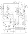
- FIG. 1 is a configuration diagram of an electronic control device according to a first embodiment of the present invention.
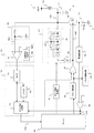
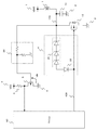
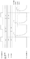
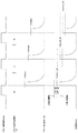
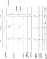
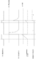
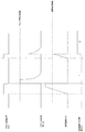
- FIG. It is a block diagram of the electronic controller which is the 2nd Example of this invention. It is a block diagram of the electronic controller which is the 3rd Example of this invention. It is a block diagram of the electronic controller which is the 4th Example of this invention. It is a block diagram of the conventional electronic control apparatus. It is a timing chart explaining clamp voltage change operation of the 1st example. It is a timing chart explaining the determination threshold value change adjustment operation of the first embodiment. It is a timing chart explaining clamp voltage detection operation of the 1st example. It is a timing chart explaining the drive pulse width detection operation
- FIG. 1 is a block diagram of an electronic control device for driving a dielectric load according to the first embodiment.
- the electronic control device of the present embodiment includes an inductive load 10 connected to the battery power supply 1, a switch element 12 that controls energization of the inductive load 10, a driver drive unit 42 that drives the switch element 12, Voltage divider 30, voltage clamp unit 20 that clamps the back electromotive force due to the dielectric load to a constant voltage, voltage detector 50 that detects an abnormality in the clamp voltage, and detection timing control that controls the timing to detect the clamp voltage
- the unit 40 is configured.
- the electronic control unit controls the energization to the dielectric load 10 by driving the corresponding switch element 12 by the driver driving unit 42 in accordance with a command from the microcomputer 60.
- the switch element 12 When the driver drive signal 42A output from the driver drive unit 42 becomes high level, the switch element 12 is turned on and the inductive load 10 is energized. Thereafter, when the driver drive signal 42A becomes low level, the switch element 12 is turned off, and the energization to the inductive load 10 is stopped. At this time, a counter electromotive force is generated in the driver output signal 12A due to the counter electromotive force of the dielectric load 10. The counter electromotive voltage is clamped to a predetermined voltage by the voltage clamp unit 20. A voltage clamping operation of the voltage clamping unit 20 will be described.
- the Zener diode 21 When the driver output signal 12A becomes equal to or higher than the set clamp voltage due to the back electromotive force of the inductive load 10, the Zener diode 21 is turned on and the potential of the driver drive signal 42A is pushed up. Thereafter, when the potential of the driver drive signal 42A reaches the ON threshold value of the switch element 12, the switch element 12 is turned ON, the charge stored in the capacitor 11 moves to the ground power supply 2, and the potential of the driver output signal 12A decreases. As a result, when the potential of the driver output signal 12A becomes equal to or lower than the set clamp voltage, the switch element 12 is turned off. By this series of operations, the voltage of the driver output signal 12A is clamped to a constant value, and the switch element 12 is prevented from being destroyed by the overvoltage.
- the voltage clamp part 20 needs to protect the switch element 12 from overvoltage destruction regardless of whether the battery power supply 1 is turned on. Therefore, the voltage clamp unit 20 performs the clamping operation even when the power source 1 is not turned on.
- the clamp voltage of an electronic control device that drives an inductive load has different specifications required for each driven load. Therefore, the clamp voltage has been optimized according to the specifications of the driven load.
- the specifications of electronic control devices have been made more flexible, and electronic control devices that drive electronic loads including inductive loads can also handle various loads. Therefore, it is required to improve the output expandability of the electronic control device by making the clamp voltage specification flexible.
- the voltage clamp unit 20 of this embodiment has a configuration in which the clamp voltage can be changed according to the load to be driven.
- the voltage clamp unit 20 includes a Zener diode 21, a switch 23 connected so that the number of connections between the diode 22 and the Zener diode 21 can be changed, and controls the switches 23A and 23B by a clamp voltage control signal 41A.
- the number of Zener diodes connected can be changed.
- FIG. 6 shows a timing chart when changing the clamp voltage.
- the clamp voltage control signal 41A is “00”
- both the switches 23A and 23B are set to OFF, and the back electromotive voltage is clamped by Vclamp1 as shown in 7-1.
- the clamp voltage control signal 41A When the clamp voltage control signal 41A is “01”, the switch 23A is set to OFF, the switch 23B is set to ON, and the back electromotive voltage is clamped by Vclamp2 as indicated by 7-2.
- the clamp voltage control signal 41A When the clamp voltage control signal 41A is “10”, the switches 23A and 23B are both turned on, and the back electromotive voltage is clamped by Vclamp3 as shown in 7-3.
- the clamp voltage setting is held while the battery power supply 1 is turned on by the clamp voltage control unit.
- the clamp voltage can be changed by controlling the switch 23 and changing the number of Zener diodes connected according to the load.
- the abnormality of the clamp voltage is detected by comparing the clamp voltage divided by the voltage dividing resistor 30 with the voltage determination threshold in the voltage detection unit 50.
- the clamp voltage detection unit 50 latches the comparators 51 and 52, the determination threshold generation units 53 and 54 that generate the determination threshold voltage of the comparator according to the setting of the clamp voltage, and the output of the comparator at a predetermined timing.
- the two flip-flop circuits 55 and 56 and a clamp voltage determination unit 57 that determines a clamp voltage abnormality from the comparison result of the comparator.
- the clamp voltage control signal 41A When the clamp voltage control signal 41A is “00”, the clamp voltage is set to Vclamp1. At this time, the upper limit determination threshold is a potential higher by ⁇ v1 than the clamp voltage Vclamp1_div divided by the voltage dividing resistor 30, and the lower limit determination threshold is ⁇ v1 with respect to the clamp voltage Vclamp1_div divided by the voltage dividing resistor 30. Is only set at a lower potential. Similarly, when the clamp voltage control signal 41A is “01”, the upper limit determination threshold is set to a potential that is ⁇ v1 higher than Vclamp2_div, and the lower limit determination threshold is set to a potential that is ⁇ v1 lower than Vclamp2_div.
- the upper limit determination threshold is set to a potential that is ⁇ v1 higher than Vclamp3_div
- the lower limit determination threshold is set to a potential that is lower by ⁇ v1 than Vclamp3_div.
- FIG. 8 shows a timing chart of clamp voltage detection.
- the driver output signal 12A is clamped to a predetermined clamp voltage by the clamp unit 20.
- the voltage of the driver output signal 12A is divided by the voltage dividing resistor 30 and compared with the upper / lower limit determination threshold by the comparators 51 and 52.
- the comparison result with the upper limit determination threshold is low level, and the comparison result with the lower limit determination threshold is high level.
- the comparison result with the upper and lower limit determination threshold is fetched into the subsequent flip-flop circuits 55 and 56 by the detection timing signal 40A generated at the falling timing of the driver drive signal 42A and input to the clamp voltage determination unit 57. .
- the clamp voltage determination unit 57 determines that the comparison result with the upper limit determination threshold value stored in the flip-flop circuits 55 and 56 is low level and the comparison result with the lower limit determination threshold value is high level, and notifies the microcomputer 60 of the result. To do. Next, for example, an operation when the Zener diode 21A in the clamp unit 20 is short-circuited and the clamp voltage becomes low will be described.
- the clamp unit 20 clamps the driver output signal 12A to a potential lower by a Zener voltage (Vz) of the Zener diode 21A short-circuited from a predetermined clamp voltage. .
- the voltage of the driver output signal 12A is divided by the voltage dividing resistor 30 and compared with the upper / lower limit determination threshold by the comparators 51 and 52.
- a low voltage abnormality of the clamp voltage due to a short circuit of the Zener diode 21A occurs, a low level is output as a result of comparison with the upper and lower determination thresholds.
- the comparison result with the upper and lower limit determination threshold is fetched into the subsequent flip-flop circuits 55 and 56 by the detection timing signal 40A generated at the falling timing of the driver drive signal 42A and input to the clamp voltage determination unit 57.
- the clamp voltage determination unit 57 determines that the low voltage is abnormal and notifies the microcomputer 60 of it.
- the driver output signal 12 ⁇ / b> A is not clamped by the clamp unit 20, and thus becomes a voltage higher than a predetermined clamp voltage.
- the voltage of the driver output signal 12A is divided by the voltage dividing resistor 30 and compared with the upper / lower limit determination threshold by the comparators 51 and 52.
- both of the comparison results with the upper limit and lower limit determination threshold are output at a high level.
- the comparison result with the upper and lower limit determination threshold is fetched into the subsequent flip-flop circuits 55 and 56 by the detection timing signal 40A generated at the falling timing of the driver drive signal 42A and input to the clamp voltage determination unit 57. .
- the clamp voltage determination unit 57 determines that the overvoltage is abnormal when the comparison result between the upper limit and lower limit determination threshold values stored in the flip-flop circuits 55 and 56 is high, and notifies the microcomputer 60 of the determination. In this way, at least two voltage determination thresholds and a voltage dividing resistor are provided, and the clamp voltage divided by the voltage dividing resistor is compared with at least two voltage determination thresholds, respectively. It is possible to detect various abnormalities and improve the reliability of the electronic control device.
- the present embodiment also has the following effects as the second effect.
- the Zener diode 21 of the voltage clamp unit 20 is turned on, and the switch element 12 is turned on by pushing up the gate voltage of the switch element 12.
- the electric charge stored in the switch element 12 is released to the ground, and the potential of the driver output signal 12A is lowered to prevent overvoltage breakdown of the switch element 12 due to the back electromotive voltage of the switch element 12.
- the zener diode 21A in the clamp unit 20 has an open failure, since the voltage clamp operation by the voltage clamp unit 20 cannot be performed, a counter electromotive voltage exceeding a predetermined clamp voltage is generated, and the switch element 12 is destroyed. There is a problem of being done.
- a spare voltage clamping function for preventing overvoltage breakdown of the switch element 12 by forcibly turning on the switch element 12 when an overvoltage abnormality of the clamp voltage is detected.
- the spare voltage clamp function will be described.
- the outputs of the comparators 51 and 52 are input to the AND gate 45.
- the AND gate When both the outputs of the comparators 51 and 52 are at a high level, the AND gate outputs a high level.
- the output of the AND gate 45 is input to the OR gate 47, and when the output of the AND gate 45 is high level, the OR gate 47 outputs high level.
- the output of the OR gate 47 is connected to the switch element 12, and when the output of the OR gate 47 becomes high level, the switch element 12 is turned on. As a result, the electric charge stored in the capacitor 11 moves to the ground power source 2 via the switch element 12, and the potential of the driver output signal 12A decreases.
- this embodiment also has the following effects as a third effect.
- the clamp voltage may not reach the set value because the energy stored in the inductive load 10 is small. In this case, there is a possibility that a low voltage abnormality of the clamp voltage is erroneously detected even if there is no problem in the voltage clamp unit 20.
- a pulse width detection unit 44 and a current detection unit 43 are provided, and the time during which the dielectric load 10 is energized and the current flowing through the dielectric load are measured. Detect short-time load energies that may cause false detections. FIG.
- the pulse width detector 44 shows a timing chart of the pulse width detection operation by the pulse width detector 44.
- the energization time of the dielectric load 10 is measured by the pulse width detector 44.
- the pulse width detector 44 is a timer having a timer threshold, and measures the time during which the driver drive signal 42A is kept at the high level.
- the pulse width detector 44 drives the determination result mask signal 43A to a low level.
- the determination result mask signal 43A is driven to a high level.
- the determination result mask signal 43A is input to the clamp voltage determination unit 57, and masks the outputs of the flip-flop circuits 55 and 56 when the determination result mask signal 43A is at a high level. It is also possible to mask the output of the clamp voltage determination unit by inputting the determination result mask signal 43A to the microcomputer.
- FIG. 10 shows a timing chart of the current detection unit 43. The current flowing through the dielectric load 10 is measured by the current detection unit 43. The current detection unit 43 has a predetermined load current threshold, and compares the load current threshold with the load current 13 ⁇ / b> A flowing through the dielectric load 10.
- the current detection unit 43 drives the determination result mask signal 43A to a low level.
- the determination result mask signal 43A is driven to a high level.
- the determination result mask signal 43A is input to the clamp voltage determination unit 57, and masks the outputs of the flip-flop circuits 55 and 56 when the determination result mask signal 43A is at a high level. It is also possible to mask the output of the clamp voltage determination unit by inputting the determination result mask signal 43A to the microcomputer.
- this embodiment also has the following effects as a fourth effect.
- the counter electromotive voltage generated by stopping the energization of the dielectric load 10 is clamped to a predetermined voltage by the clamp unit 20, but the energy stored in the dielectric load 10 is consumed earlier as the clamp voltage is higher.
- the period during which the voltage is clamped is short when the clamp voltage is high and long when the clamp voltage is low.
- FIG. 11 shows a timing chart of the pulse width changing operation of the detection timing signal 40A according to the clamp voltage setting.
- the relationship between the pulse widths of the detection timing signals (T1 to T3) shown below is T1 ⁇ T2 ⁇ T3.
- the clamp voltage control signal 41A is “00”
- the clamp voltage is set to Vclamp1.
- the pulse width of the detection timing signal 40A is set to a predetermined pulse width T1.
- the clamp voltage control signal 41A becomes “01”
- the clamp voltage is set to Vclamp2 having a potential lower than Vclamp1
- the pulse width of the detection timing signal 40A is set to T2 having a pulse width longer than T1.
- the clamp voltage control signal 41A becomes “10”
- the clamp voltage is set to Vclamp3 whose potential is lower than Vclamp2
- the pulse width of the detection timing signal 40A is set to T3, which is longer than T2.
- the comparison results of the comparators 51 and 52 can be taken into the flip-flops 55 and 56 at the correct timing according to the clamp voltage setting.
- the abnormality of the clamp voltage is detected by comparing the two voltage determination thresholds with the divided potential of the clamp voltage.
- three or more voltage determination thresholds and the divided potential of the clamp voltage are detected. It is clear that a similar effect can be expected by comparing the two.
- FIG. 2 is a block diagram of an electronic control device for driving an inductive load according to the second embodiment.
- This embodiment is different from the first embodiment in the configuration of the clamp voltage detector 50.
- one voltage dividing resistor 30 and two comparators 51 and 52 to which upper and lower limit determination threshold values are input are provided, and the clamp voltage divided by the voltage dividing resistor 30 and the upper and lower limit determination threshold values are set.
- the clamp voltage abnormality is detected by comparing each.
- the second embodiment includes two voltage dividing resistors 31 and 32 having different voltage dividing ratios and two comparators 51 and 52 to which a reference voltage signal 58A is input. The difference is that the clamp voltage abnormality is detected by comparing the two divided voltages with the reference voltage signal 58A.
- the clamp voltage detector 50 of the present embodiment includes two voltage dividing resistors 31 and 32 having different voltage dividing ratios, comparators 51 and 52, a reference voltage generator 58, two flip-flop circuits 55 and 56, and a clamp voltage determination unit 57. It consists of The voltage dividing resistors 31 and 32 can be changed to different voltage dividing ratios by changing the number of resistors connected by the switches 33 and 34, respectively.
- FIG. 12 shows a timing chart of the voltage dividing ratio changing operation of the voltage dividing resistors 31 and 32 according to the clamp voltage setting. When the clamp voltage control signal 41A is “00”, the clamp voltage is set to Vclamp1.
- the switches 33A and 34A are set ON, and the switches 33B and 34B are set ON.
- the driver output signal 12A is reduced to a potential lower than the reference voltage signal 58A by a predetermined voltage ( ⁇ v2) by the voltage dividing resistor 31, and the predetermined voltage ( ⁇ v2) is supplied to the reference voltage signal 58A by the voltage dividing resistor 32. ) Is divided to a higher potential.
- the clamp voltage control signal 41A is “01”
- the clamp voltage is set to Vclamp2.
- the switches 33A and 34A are set to ON, and the switches 33B and 34B are set to OFF.
- the driver output signal 12A is reduced to a potential lower than the reference voltage signal 58A by a predetermined voltage ( ⁇ v2) by the voltage dividing resistor 31, and the predetermined voltage ( ⁇ v2) is supplied to the reference voltage signal 58A by the voltage dividing resistor 32. ) Is divided to a higher potential.
- the clamp voltage control signal 41A is “10”
- the clamp voltage is set to Vclamp3.
- the switches 33A and 34A are set to OFF, and the switches 33B and 34B are set to OFF.
- the driver output signal 12A is reduced to a potential lower than the reference voltage signal 58A by a predetermined voltage ( ⁇ v2) by the voltage dividing resistor 31, and the predetermined voltage ( ⁇ v2) is supplied to the reference voltage signal 58A by the voltage dividing resistor 32. ) Is divided to a higher potential.
- the clamp voltage can be diagnosed according to the clamp voltage by controlling the voltage division ratio so that the potential difference between the divided clamp voltage and the reference voltage signal 58A is constant. It becomes.
- FIG. 13 shows a timing chart of the clamp voltage detection operation. First, the operation during normal operation will be described.
- the driver output 12 ⁇ / b> A is clamped to a predetermined clamp voltage by the voltage clamp unit 20.
- the voltage of the driver output signal 12A is divided by different voltage dividing ratios by the voltage dividing resistors 31 and 32, and is compared with the reference voltage signal 58A by the comparators 51 and 52.
- the comparison result between the divided signal 31A and the reference voltage signal 58A is low level, and the comparison result between the divided signal 32A and the reference voltage signal 58A is high level.
- the comparison result with the reference voltage signal 58A is taken into the subsequent flip-flop circuits 55 and 56 by the detection timing signal 40A generated at the falling timing of the driver drive signal 42A and input to the clamp voltage determination unit 57.
- the clamp voltage determination unit 57 determines that the output is normal and notifies the microcomputer 60 of it.
- the driver output signal 12A When a back electromotive force is generated by stopping energization of the dielectric load 10, the driver output signal 12A is clamped to a potential lower by a Zener voltage (Vz) of the Zener diode 21A short-circuited from a predetermined clamp voltage by the voltage clamp unit 20.
- the voltage of the driver output signal 12A is divided at different voltage dividing ratios by the voltage dividing resistors 31 and 32, and is compared with the reference voltage signal 58A by the comparators 51 and 52.
- the comparison result between the divided voltage signal 31A and the divided signal 32A and the reference voltage signal 58A is output at a low level.
- the comparison result with the reference voltage signal 58A is taken into the subsequent flip-flop circuits 55 and 56 by the detection timing signal 40A generated at the falling timing of the driver drive signal 42A and input to the clamp voltage determination unit 57.
- the clamp voltage determination unit 57 determines that the low voltage is abnormal and notifies the microcomputer 60 of it.
- the driver output signal 12 ⁇ / b> A is not clamped by the voltage clamp unit 20, and thus becomes a voltage higher than a predetermined clamp voltage.
- the voltage of the driver output signal 12A is divided at different voltage dividing ratios by the voltage dividing resistors 31 and 32, and is compared with the reference voltage signal 58A by the comparators 51 and 52.
- the comparison result between the divided signals 31A and 32A and the reference voltage signal 58A is output at a high level.
- the comparison result with the reference voltage signal 58A is taken into the subsequent flip-flop circuits 55 and 56 by the detection timing signal 40A generated at the falling timing of the driver drive signal 42A and input to the clamp voltage determination unit 57.
- the clamp voltage determination unit 57 determines that the overvoltage is abnormal and notifies the microcomputer 60 of it.
- the voltage dividing resistors 31 and 32 capable of adjusting the voltage dividing ratio and the two comparators 51 and 52 to which the reference voltage is input are provided, and the voltage dividing signal and the reference divided by the voltage dividing resistors at different voltage dividing ratios, respectively.
- failure diagnosis according to the clamp voltage can be performed as in the first embodiment.
- an abnormality in the clamp voltage is detected by comparing one voltage determination threshold value with two divided potentials divided by the voltage dividing resistor.
- three or more voltage determination threshold values are detected. It is clear that the same effect can be expected by comparing the divided potential of the clamp voltage.
- FIG. 3 is a block diagram of an electronic control device for driving an inductive load according to the third embodiment.
- the clamp voltage abnormality is detected by directly measuring the divided potential of the clamp voltage.
- the electronic control device according to this embodiment includes an inductive load 10 connected to the battery power source 1, a switch element 12 that controls energization of the inductive load 10, a voltage dividing resistor 30, and a back electromotive force generated by the dielectric load 10.
- the voltage clamp unit 20 clamps the voltage to a constant voltage
- the voltage detection unit 50 detects the clamp voltage abnormality
- the time measurement unit 70 measures the period during which the back electromotive voltage is generated. Functions other than the voltage detection unit 50 and the time measurement unit 70 are the same as those in the first embodiment. In the following description of the present embodiment, portions that are the same as those described in the first embodiment are omitted.
- the clamp voltage detector 50 is a comparator 51 to which a reference voltage signal 58A is input.
- the comparator 51 compares the divided voltage signal 30A obtained by dividing the voltage of the driver output signal 12A with the voltage dividing resistor 30 with the reference voltage signal 58A. While the divided potential exceeds the reference voltage signal 58A, a high level is output.
- the time measurement unit 70 includes two timers (measurement timer 71 and expected value timer 72) and a counter comparison unit 73 that compares the count values of the timers, and the output of the voltage detection unit 50 is high level. Measure the period of time with a timer and detect the clamp voltage failure by comparing it with the expected value range.
- FIG. 14 shows a timing chart of the clamp voltage detection operation.
- the output of the voltage detection unit 50 becomes high level.
- the expected value timer 72 starts counting. Thereafter, when the potential of the driver output signal 12A decreases and the potential of the divided signal 30A becomes equal to or lower than the reference voltage signal 58A, the output of the voltage detection unit 50 becomes low level.
- the expected value timer 72 stops counting and holds the count value.
- the expected value range of the back electromotive voltage generation time is calculated based on the counter value of the held expected value timer 72.
- the learning mode signal 60A becomes low level
- the mode shifts to the determination mode.
- the determination mode when a back electromotive voltage is generated and the potential of the divided signal 30A obtained by dividing the driver output signal 12A by the voltage dividing resistor 30 becomes equal to or higher than the reference voltage signal 58A, the output of the voltage detection unit 50 becomes high level. .
- the measurement timer 71 starts counting.
- the output of the voltage detection unit 50 becomes low level.
- the measurement timer 71 stops counting.
- the counter comparison unit 73 compares the count value of the measurement timer 71 with the expected value range calculated in the learning mode.
- the counter value of the measurement timer 71 is within the expected value range, it is normal, when it is below the expected value range, it detects a low voltage, and when it is above the expected value range, it detects an overvoltage and outputs a clamp period determination signal 73A to the microcomputer 60. To do.
- the clamp voltage is not directly measured as in the first and second embodiments, but the time during which the divided potential of the back electromotive voltage exceeds the predetermined voltage is measured in advance and compared with the latest measured value. By doing so, it is possible to detect a clamp voltage failure.
- the clamp voltage abnormality is detected by detecting with a timer the time that exceeds the clamp voltage divided by the voltage dividing resistor and the predetermined voltage threshold generated by the reference voltage generation unit.
- a variable voltage generation unit instead of the reference voltage generation unit 58 and changing the voltage threshold according to the clamp voltage setting, it is possible to expect more stable detection especially when the clamp voltage is set to a low voltage. It is obvious.
- this embodiment also has the following effects as the second effect.
- the present embodiment includes two timers (measurement timer 71 and expected value timer 72), and measures the time when the clamp voltage exceeds a predetermined voltage in advance by the expected value timer 72, and then measures the measurement timer.
- the clamp voltage is detected by comparing with the time similarly measured at 71.
- FIG. 15 shows a timing chart of the timer failure detection operation.
- the potential of the divided signal 30A becomes equal to or higher than the reference voltage signal 58A, and the output of the voltage detection unit 50 becomes high level, not only the expected value timer 72 but also the measurement timer. 71 also starts counting at the same timing. Thereafter, as the potential of the output signal 12A decreases, when the potential of the divided signal 30A decreases and falls below the potential of the reference voltage signal 58A, the output of the voltage detector 50 becomes low level. When the output of the voltage detection unit 50 becomes low level, both the measurement timer 71 and the expected value timer 72 stop counting.
- the clamp period determination unit 73 compares the count values of the measurement timer 71 and the expected value timer 72, and if the count values differ significantly, it is determined that one of the timers has failed, and the microcomputer 60 is notified.
- timer failure detection can be performed by monitoring the count values of the two timers.
- FIG. 4 is a block diagram of an electronic control device for driving an inductive load according to the fourth embodiment.
- the fourth embodiment is the same as the third embodiment in that the time during which the back electromotive voltage exceeds the predetermined voltage threshold is measured and the clamp voltage abnormality is performed by comparing with the expected value range.
- the range calculation method is different from that of the third embodiment.
- the expected value range is calculated from one measurement value measured in the learning mode, but in the fourth embodiment, the generation time of the back electromotive voltage measured in the past load driving is calculated.
- the difference is that the expected value range is calculated from the past measured values stored in the register. Since the present embodiment is different from the third embodiment only in the configuration of the time measuring unit 70, the description of other configurations is omitted.
- the time measurement unit 70 includes a timer 74, a counter comparison unit 73 that compares the count value of the timer, and a register 75 that stores the count value of the timer, and the output of the voltage detection unit 50 becomes high level.
- a clamp voltage failure is detected by measuring a certain period with a timer and comparing it with an expected value range calculated from a counter value stored in a register.
- FIG. 16 shows a timing chart of the clamp voltage detection operation. After the battery voltage 1 is turned on, when the switch element 12A is turned off by the driver drive signal 42A and the energization to the dielectric load 10 is stopped, a counter electromotive voltage is generated.
- the comparator output signal 51A becomes high level.
- the timer 74 starts counting. Thereafter, when the potential of the driver output signal 12A decreases, the potential of the divided signal 30A becomes equal to or lower than the reference voltage signal 58A, and the comparator output signal 51A becomes low level, the timer 74 stops counting and stores the counter value in the register 75. To do.
- the register 75 stores counter values for a predetermined number of times of driving.
- the counter comparison unit 73 calculates an expected value range from the counter value stored in the register.
- the counter comparison unit 73 calculates the expected value range and compares it with the latest count value.
- the latest counter value is included in the expected value range, it is normal, when it is below the expected value range, a low voltage is detected, and when it is above the expected value range, an overvoltage is detected, and a clamp period determination signal 73A is output to the microcomputer 60.
- the reverse voltage generation time is not previously learned as in the third embodiment.
- the clamp voltage abnormality is detected by detecting with a timer the time that exceeds the clamp voltage divided by the voltage dividing resistor and the predetermined voltage threshold generated by the reference voltage generation unit. It is clear that a more stable detection can be expected by providing a variable voltage generator instead of the reference voltage generator and changing the voltage threshold according to the clamp voltage setting, especially when the clamp voltage is set to a low voltage. It is.
- this invention is not limited to an above-described Example, Various modifications are included. For example, the above-described embodiments have been described in detail for easy understanding of the present invention, and are not necessarily limited to those having all the configurations described.
- a part of the configuration of one embodiment can be replaced with the configuration of another embodiment, and the configuration of another embodiment can be added to the configuration of one embodiment. Further, it is possible to add, delete, and replace other configurations for a part of the configuration of each embodiment. Further, the signal lines indicate that they are considered necessary for the explanation, and do not necessarily indicate all the signal lines necessary for the product.
Landscapes
- Electronic Switches (AREA)
Abstract
従来の電子制御装置は、1つの電圧判定閾値にて電圧検出を行うため、誘導性負荷の開放故障、あるいは、クランプ手段の短絡故障によるクランプ電圧の低電圧異常の検出、または、クランプ手段内部のツェナーダイオードの開放故障によるクランプ電圧の過電圧故障のどちらかしか検出が出来ないという課題があった。 前述の課題を解決するため、本発明では、少なくとも2つの電圧判定閾値により電圧検出を行う電圧検出手段と、クランプ電圧設定に応じて、電圧判定閾値を変更できる電圧判定閾値生成部を備えた電子制御装置を提案する。本発明によれば、電圧分圧手段により分圧されたクランプ電圧と少なくとも2つの電圧判定閾値とをそれぞれ比較することで、クランプ電圧の低電圧異常、過電圧異常など従来の電子制御装置に比べ、多様な故障の検出ができる。さらに、クランプ電圧に応じて電圧検出手段の電圧判定閾値を変更することで、クランプ電圧の設定値に応じたクランプ電圧の診断が可能となる。
Description
本発明は、誘電性負荷を含んだ多くの電子負荷を駆動する電子制御装置に関する。
ガソリンや軽油等を燃料とする自動車、オートバイ、農耕機械、船舶機などの内燃機関の電子制御駆動装置では、インジェクタ、フュエルポンプ、ソレノイド、リレーなど、多くの誘導性負荷を駆動している。これらの誘電性負荷はスイッチにより通電を制御することで駆動されるが、スイッチにより誘電性負荷の通電が停止されると、誘電性負荷の逆起電力による逆起電圧が発生する。この逆起電圧による素子破壊を防止するため、誘電性負荷を含む電子負荷を駆動する電子制御装置では、逆起電圧を一定電圧にクランプする電圧クランプ手段を備えている。このクランプ手段により一定値にクランプされた電圧をクランプ電圧と呼んでいる。
特に、自動車の電子制御装置では、自動車に求められる安全要求に対応するため、電子制御装置の異常発生を監視し、何らかのフェイルセーフを行う診断手段を備えている。
誘電性負荷を含む電子負荷を駆動する電子制御装置においても、従来から負荷の断線を検知する目的でクランプ電圧の検出が行われてきた。クランプ電圧の検出機構を備えた電子制御装置として、特許文献1に示される電子制御装置が公知である。
誘電性負荷を含む電子負荷を駆動する電子制御装置においても、従来から負荷の断線を検知する目的でクランプ電圧の検出が行われてきた。クランプ電圧の検出機構を備えた電子制御装置として、特許文献1に示される電子制御装置が公知である。
図5に特許文献1に示される従来の誘導性負荷を含む電子負荷を駆動する電子制御装置の構成図を示す。
図5に示される従来の誘電性負荷を有する電子負荷を駆動する電子制御装置は、分圧抵抗30と誘電性負荷への通電を制御するスイッチ12と、電圧検出用のセンスMOSトランジスタ5を備え、分圧抵抗30により分圧されたクランプ電圧とセンスMOSトランジスタ5の電圧閾値とを比較することで負荷の断線の検出を行う。
図5に示される従来の電子制御装置は、1つの電圧判定閾値にてクランプ電圧検出を行うため、誘導性負荷を含む電子負荷の開放故障、あるいは、クランプ手段の短絡故障によるクランプ電圧の低電圧異常の検出、または、電圧クランプ手段内部のツェナーダイオードの開放故障によるクランプ電圧の過電圧故障のどちらかしか検出が出来ないという課題があった。
また、従来の電子制御装置のクランプ電圧の電圧判定閾値は、センスMOSトランジスタの特性により決まるため、負荷に応じてクランプ電圧を変更する場合は、クランプ電圧に応じたクランプ電圧の異常診断が出来ないという課題があった。
また、従来の電子制御装置のクランプ電圧の電圧判定閾値は、センスMOSトランジスタの特性により決まるため、負荷に応じてクランプ電圧を変更する場合は、クランプ電圧に応じたクランプ電圧の異常診断が出来ないという課題があった。
前述の課題を解決するため、本発明では、少なくとも2つの電圧判定閾値により電圧検出を行う電圧検出手段と、クランプ電圧設定に応じて電圧判定閾値を変更できる電圧判定閾値生成部を備えた電子制御装置を提案する。本発明によれば、クランプ電圧と少なくとも2つの電圧判定閾値とをそれぞれ比較することで、クランプ電圧の低電圧異常、過電圧異常など従来の電子制御装置に比べ、多様な故障の検出ができる。
また、クランプ電圧に応じて電圧検出手段の電圧判定閾値を変更することで、駆動する負荷に合わせてクランプ電圧を変更する場合においても、クランプ電圧の設定値に応じたクランプ電圧の診断が可能となる。
また、クランプ電圧に応じて電圧検出手段の電圧判定閾値を変更することで、駆動する負荷に合わせてクランプ電圧を変更する場合においても、クランプ電圧の設定値に応じたクランプ電圧の診断が可能となる。
少なくとも2つの電圧判定閾値によりクランプ電圧の過電圧、低電圧の検出を行うことで、クランプ電圧手段が正常に動作しているかを診断でき、電子制御装置の信頼性を向上させることができる。
クランプ電圧に合わせて電圧判定閾値を変更することで、クランプ電圧設定に応じたクランプ電圧の診断が可能となる。
クランプ電圧に合わせて電圧判定閾値を変更することで、クランプ電圧設定に応じたクランプ電圧の診断が可能となる。
以下、実施例について図面を用いて説明する。
図1は第1の実施例である誘電性負荷を駆動する電子制御装置の構成図である。
本実施例の電子制御装置は、バッテリー電源1に接続された誘導性負荷10と、前記誘導性負荷10の通電を制御するスイッチ素子12と、前記スイッチ素子12を駆動するドライバ駆動部42と、分圧抵抗30と、誘電性負荷による逆起電圧を一定の電圧にクランプする電圧クランプ部20と、クランプ電圧異常を検出する電圧検出部50と、クランプ電圧を検出するタイミングを制御する検知タイミング制御部40により構成されている。
電子制御装置はマイコン60からの命令に従い、該当するスイッチ素子12をドライバ駆動部42により駆動することで、誘電性負荷10への通電を制御する。
ドライバ駆動部42から出力されるドライバ駆動信号42Aがハイレベルになると、スイッチ素子12がオンされ、誘導性負荷10が通電される。その後、ドライバ駆動信号42Aがロウレベルとなると、スイッチ素子12がオフされ、誘導性負荷10への通電が停止される。この時、誘電性負荷10の逆起電力により、ドライバ出力信号12Aには逆起電圧が発生する。この逆起電圧は電圧クランプ部20により所定の電圧にクランプされる。
電圧クランプ部20の電圧クランプ動作について説明する。
誘導性負荷10の逆起電力により、ドライバ出力信号12Aが設定されたクランプ電圧以上になると、ツェナーダイオード21がオンし、ドライバ駆動信号42Aの電位が押し上げられる。その後、ドライバ駆動信号42Aの電位がスイッチ素子12のオン閾値に達すると、スイッチ素子12がオンし、コンデンサ11に蓄えられた電荷がグラウンド電源2に移動し、ドライバ出力信号12Aの電位が下がる。これにより、ドライバ出力信号12Aの電位が設定されたクランプ電圧以下となると、スイッチ素子12はオフされる。この一連の動作により、ドライバ出力信号12Aの電圧は一定値にクランプされ、スイッチ素子12の過電圧による破壊が防止される。
また、電圧クランプ部20は、バッテリー電源1の電源投入の有無に関わらず、スイッチ素子12を過電圧破壊から保護する必要がある。そのため、電圧クランプ部20は、電源1の電源投入されていない場合においてもクランプ動作を行う。
従来、誘導負荷を駆動する電子制御装置のクランプ電圧は駆動される負荷毎に要求される仕様が異なるため、駆動される負荷の仕様に応じたクランプ電圧の最適化が行われていた。
しかし、近年は多くの顧客仕様に対応するため、電子制御装置の仕様のフレキシブル化が進められており、誘導性負荷を含む電子負荷を駆動する電子制御装置においても、多様な負荷の駆動に対応するため、クランプ電圧仕様のフレキシブル化による電子制御装置の出力拡張性の向上が求められている。
本実施例の電圧クランプ部20はこの要求を達成するため、駆動する負荷に応じてクランプ電圧を変更可能な構成となっている。
電圧クランプ部20は、ツェナーダイオード21とダイオード22とツェナーダイオード21の接続数を変更できるように接続されたスイッチ23により構成されており、クランプ電圧制御信号41Aにより、スイッチ23A、23Bを制御することで、ツェナーダイオードの接続数を変更可能な構成となっている。これによりクランプ電圧の変更ができる。
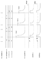
図6にクランプ電圧変更時のタイミングチャートを示す。
クランプ電圧制御信号41Aが”00”のとき、スイッチ23A、23Bともオフに設定され、逆起電圧は7-1に示すようにVclamp1でクランプされる。
クランプ電圧制御信号41Aが”01”のとき、スイッチ23Aはオフ、スイッチ23Bはオンに設定され、逆起電圧は7-2に示すようにVclamp2でクランプされる。
クランプ電圧制御信号41Aが”10”のとき、スイッチ23A、23Bともオンに設定され、逆起電圧は、7-3に示すようにVclamp3でクランプされる。
クランプ電圧設定は、クランプ電圧制御部によりバッテリー電源1が投入されている間、保持される。このように負荷に応じて、スイッチ23を制御し、ツェナーダイオードの接続数を変更することで、クランプ電圧を変更することができる。
このように、クランプ電圧制御信号41Aによりクランプ電圧を変更可能な構成とすることで、クランプ電圧の要求仕様が異なる電子負荷の駆動が可能となり、電子制御装置の出力拡張性を向上させるといった効果が期待できる。
クランプ電圧異常の検出は、分圧抵抗30により分圧されたクランプ電圧と、電圧判定閾値を電圧検出部50において比較することにより行われる。
クランプ電圧検出部50は、2つのコンパレータ51、52と、クランプ電圧の設定に応じて、コンパレータの判定閾値電圧を生成する判定閾値生成部53、54と、コンパレータの出力を所定のタイミングでラッチする2つのフリップフロップ回路55,56と、コンパレータの比較結果からクランプ電圧異常の判定を行うクランプ電圧判定部57により構成されている。
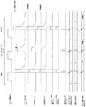
図7にクランプ電圧設定に応じた判定閾値の変更動作のタイミングチャートを示す。
クランプ電圧制御信号41Aが”00”のとき、クランプ電圧は、Vclamp1に設定されている。この時、上限判定閾値は分圧抵抗30により分圧されたクランプ電圧Vclamp1_divに対し、Δv1だけ上の電位に、下限判定閾値は、分圧抵抗30により分圧されたクランプ電圧Vclamp1_divに対し、Δv1だけ下の電位に設定される。
クランプ電圧制御信号41Aが”01”のときも同様に、上限判定閾値は、Vclamp2_divに対し、Δv1だけ上の電位に、下限判定閾値は、Vclamp2_divに対し、Δv1だけ、下の電位に設定される。
クランプ電圧制御信号41Aが”10”のときも同様に、上限判定閾値は、Vclamp3_divに対し、Δv1だけ上の電位に、下限判定閾値は、Vclamp3_divに対し、Δv1だけ下の電位に設定される。
このように、クランプ電圧に合わせて判定閾値を変更することで、クランプ電圧設定に応じたクランプ電圧の診断が可能となる。
クランプ電圧検出の動作について説明する。
スイッチ素子12がオフされたタイミングで発生したクランプ電圧は、分圧抵抗30により分圧された後、コンパレータ51,52により上下限判定閾値と比較される。
上下限判定閾値との比較結果は、検出タイミング制御信号40Aのタイミングでフリップフロップ回路55,56に取り込まれ、取り込まれたデータはクランプ電圧判定部57に入力され、クランプ電圧異常の判定が行われる。
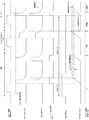
図8にクランプ電圧検出のタイミングチャートを示す。
始めに正常動作時の動作について説明する。
誘電性負荷10の通電停止により、逆起電圧が発生すると、クランプ部20により、ドライバ出力信号12Aは所定のクランプ電圧にクランプされる。このドライバ出力信号12Aの電圧は分圧抵抗30で分圧され、コンパレータ51、52により上下限判定閾値と比較される。正常動作時、上限判定閾値との比較結果はロウレベル、下限判定閾値との比較結果はハイレベルが出力される。上下限判定閾値との比較結果は、ドライバ駆動信号42Aの立下りのタイミングで生成された検知タイミング信号40Aにより、後段のフリップフロップ回路55,56に取り込まれ、クランプ電圧判定部57に入力される。クランプ電圧判定部57は、フリップフロップ回路55,56に格納された上限判定閾値との比較結果がロウレベル、下限判定閾値との比較結果がハイレベルの場合は、正常と判定し、マイコン60に通知する。
次に、例えばクランプ部20内部のツェナーダイオード21Aがショート故障し、クランプ電圧が低電圧となった場合の動作について説明する。
誘電性負荷10の通電停止により、逆起電圧が発生すると、クランプ部20により、ドライバ出力信号12Aは所定のクランプ電圧からショートしたツェナーダイオード21Aのツェナー電圧(Vz)分だけ低い電位にクランプされる。ドライバ出力信号12Aの電圧は分圧抵抗30で分圧され、コンパレータ51、52により上下限判定閾値と比較される。ツェナーダイオード21Aのショートによるクランプ電圧の低電圧異常発生時、上限及び下限判定閾値との比較結果はともにロウレベルが出力される。上下限判定閾値との比較結果は、ドライバ駆動信号42Aの立下りのタイミングで生成された検知タイミング信号40Aにより、後段のフリップフロップ回路55,56に取り込まれ、クランプ電圧判定部57に入力される。クランプ電圧判定部57は、フリップフロップ回路55,56に格納された上限及び下限判定閾値との比較結果がともにロウレベルの場合は、低電圧異常と判定し、マイコン60に通知する。
最後に、例えばクランプ部20のツェナーダイオード21Aがオープン故障し、クランプ電圧が過電圧となった場合の動作について説明する。
誘電性負荷10の通電停止により逆起電圧が発生すると、ドライバ出力信号12Aは、クランプ部20によりクランプされないため、所定のクランプ電圧以上の電圧となる。
ドライバ出力信号12Aの電圧は分圧抵抗30で分圧され、コンパレータ51、52により上下限判定閾値と比較される。ツェナーダイオード21Aのオープン故障によるクランプ電圧の過電圧異常発生時、上限及び下限判定閾値との比較結果はともにハイレベルが出力される。上下限判定閾値との比較結果は、ドライバ駆動信号42Aの立下りのタイミングで生成された検知タイミング信号40Aにより、後段のフリップフロップ回路55,56に取り込まれ、クランプ電圧判定部57に入力される。クランプ電圧判定部57は、フリップフロップ回路55,56に格納された上限及び下限判定閾値との比較結果がともにハイレベルの場合は、過電圧異常と判定し、マイコン60に通知する。
このように、少なくとも2つの電圧判定閾値と分圧抵抗を備え、分圧抵抗により分圧されたクランプ電圧と、少なくとも2つの電圧判定閾値をそれぞれ比較することで、クランプ電圧の低電圧異常、過電圧異常などの多様な検出が可能となり、電子制御装置の信頼性の向上が期待できる。
また、本実施例には第2の効果として以下の効果もある。
通常、誘電性負荷10の通電停止により逆起電圧が発生した場合、電圧クランプ部20のツェナーダイオード21が導通し、スイッチ素子12のゲート電圧を押し上げることで、スイッチ素子12をオンさせ、コンデンサ11に蓄えられた電荷をグラウンドに逃がし、ドライバ出力信号12Aの電位を下げることでスイッチ素子12の逆起電圧によるスイッチ素子12の過電圧破壊を防止している。しかし、例えば、クランプ部20内のツェナーダイオード21Aが開放故障した場合、電圧クランプ部20による電圧クランプ動作が行えないため、所定のクランプ電圧を超えた逆起電圧が発生し、スイッチ素子12が破壊されてしまうという問題がある。
本実施例では、この問題を解決するため、クランプ電圧の過電圧異常が検出された場合に、スイッチ素子12を強制的にオンさせることでスイッチ素子12の過電圧破壊を防止する予備の電圧クランプ機能を備えている。
この予備の電圧クランプ機能について説明する。
クランプ部20のツェナーダイオード21Aが開放故障した状態で、誘電性負荷10の通電が停止されると、逆起電圧が発生する。電圧クランプ部20が開放故障しているため、逆起電圧は設定されたクランプ電圧を超えて、クランプ電圧の上限判定閾値まで上昇する。逆起電圧が上限判定閾値に達すると、コンパレータ51,52は共にハイレベルを出力する。コンパレータ51、52の出力は、ANDゲート45に入力されており、コンパレータ51,52の出力がともにハイレベルの場合、ANDゲートはハイレベルを出力する。ANDゲート45の出力は、ORゲート47に入力されており、ANDゲート45の出力がハイレベルの場合、ORゲート47はハイレベルを出力する。ORゲート47の出力はスイッチ素子12に接続されており、ORゲート47の出力がハイレベルとなると、スイッチ素子12はオンされる。これにより、コンデンサ11に蓄えられた電荷がスイッチ素子12を介して、グランド電源2に移動し、ドライバ出力信号12Aの電位が下がる。
ドライバ出力信号12Aの電位が上限判定閾値以下、下限判定閾値以上の電位まで減少すると、コンパレータ51の出力はロウレベル、コンパレータ52の出力はハイレベルとなり、ANDゲート45の出力はロウレベル、次段のORゲート47の出力はロウレベルとなり、スイッチ素子12はオフされる。この一連の動作により、第2の効果として、電圧クランプ部20のツェナーダイオード21が開放故障し、電圧クランプ部20のクランプ機能が失われても、コンパレータ51,52の出力により、スイッチ素子12を制御することで、クランプ動作を行い、スイッチ素子の過電圧破壊を防止することができる。
さらに、本実施例には第3の効果として、以下の効果もある。
スイッチ素子12により誘導性負荷10が通電される時間が所定の時間より短い場合、誘導性負荷10に蓄えられるエネルギーが小さいため、クランプ電圧が設定値に達しないことがある。この場合、電圧クランプ部20に問題がなくてもクランプ電圧の低電圧異常を誤検出する恐れがある。本実施例は、このような誤検知を防止するため、パルス幅検出部44と電流検出部43を設け、誘電性負荷10が通電されている時間及び誘電性負荷に流れる電流を測定することにより、誤検知の可能性がある短時間の負荷通電を検出する。
図9にパルス幅検出部44によるパルス幅検出動作のタイミングチャートを示す。
誘電性負荷10の通電時間はパルス幅検出部44により測定される。パルス幅検出部44は、タイマ閾値を備えたタイマであり、ドライバ駆動信号42Aがハイレベルを継続している時間を測定する。
誘電性負荷10の通電時間がタイマ閾値以上の場合、パルス幅検出部44は判定結果マスク信号43Aをロウレベルにドライブする。誘電性負荷10の通電時間がタイマ閾値以下の場合は、判定結果マスク信号43Aをハイレベルにドライブする。
判定結果マスク信号43Aは、クランプ電圧判定部57に入力されており、判定結果マスク信号43Aがハイレベルの場合にフリップフロップ回路55,56の出力をマスクする。
判定結果マスク信号43Aをマイコンに入力して、クランプ電圧判定部の出力をマスクすることも可能である。
図10に電流検出部43のタイミングチャートを示す。
誘電性負荷10に流れる電流は、電流検出部43により測定される。電流検出部43は、所定の負荷電流閾値を有しており、負荷電流閾値と誘電性負荷10に流れる負荷電流13Aとの比較を行う。
スイッチ素子12がオン時に誘電性負荷10に流れる電流が、負荷電流閾値以上の場合、電流検出部43は、判定結果マスク信号43Aをロウレベルにドライブする。スイッチ素子12がオン時に誘電性負荷10に流れる電流が、負荷電流閾値以下の場合、判定結果マスク信号43Aをハイレベルにドライブする。
判定結果マスク信号43Aは、クランプ電圧判定部57に入力されており、判定結果マスク信号43Aがハイレベルの場合にフリップフロップ回路55,56の出力をマスクする。
判定結果マスク信号43Aをマイコンに入力して、クランプ電圧判定部の出力をマスクすることも可能である。
このように、第3の効果として、誘電性負荷10の通電時間または、誘電性負荷10に流れる負荷電流13Aを測定することで、誤検知の可能性がある短時間の負荷通電を検出でき、クランプ電圧異常の誤検知を防止することができる。
さらに、本実施例には第4の効果として、以下の効果もある。
誘電性負荷10の通電停止により生じた逆起電圧は、クランプ部20により所定の電圧にクランプされるが、クランプ電圧が高いほど誘電性負荷10に蓄えられたエネルギーが早く消費されるため、所定の電圧にクランプされる期間は、クランプ電圧が高いと短く、クランプ電圧が低いと長くなる。
例えば、負荷に応じてクランプ電圧を変更したことにより、所定の電圧にクランプされる期間が、検知タイミング信号40Aのパルス幅より短くなってしまった場合、クランプ期間外で判定されたコンパレータ51,52の適切でない判定出力を次段のフリップフロップ回路に取り込んで誤検知してしまう問題があった。
本実施例では、この問題を解決するため、クランプ電圧設定に合わせて、コンパレータ51、52のラッチタイミングを制御する検知タイミング信号40Aのパルス幅を調整することで、コンパレータ51,52の出力を正しいタイミングで、次段のフリップフロップ回路55,56に取り込むことができる。
図11に、クランプ電圧設定に応じた検知タイミング信号40Aのパルス幅変更動作のタイミングチャートを示す。
ちなみに、以下に示す検知タイミング信号(T1~T3)のパルス幅の大小関係は、T1<T2<T3である。
クランプ電圧制御信号41Aが”00”のとき、クランプ電圧はVclamp1に設定される。
この時、検知タイミング信号40Aのパルス幅は、所定のパルス幅T1に設定される。
クランプ電圧制御信号41Aが”01”となると、クランプ電圧がVclamp1より電位の低いVclamp2に設定され、検知タイミング信号40Aのパルス幅は、T1よりパルス幅の長い、T2に設定される。
クランプ電圧制御信号41Aが”10”となると、クランプ電圧がVclamp2より電位の低いVclamp3に設定され、検知タイミング信号40Aのパルス幅は、T2よりパルス幅の長い、T3に設定される。これにより、クランプ電圧設定に合わせて正しいタイミングでコンパレータ51、52の比較結果をフリップフロップ55,56に取り込むことができる。
このように、第4の効果として、クランプ電圧設定に合わせて、検知タイミング信号40Aのパルス幅を調整することで、コンパレータ51,52の出力の取り込みタイミングの起因による誤検知を防止することができる。
また、本実施例では、2つの電圧判定閾値とクランプ電圧の分圧電位を比較することで、クランプ電圧の異常を検出しているが、3つ以上の電圧判定閾値とクランプ電圧の分圧電位を比較することでも同様の効果を期待できることは明白である。
図2は第2の実施例である誘導性負荷を駆動する電子制御装置の構成図である。本実施例は第1の実施例とクランプ電圧検出部50の構成が異なる。
第1の実施例では、1つの分圧抵抗30と、上下限判定閾値がそれぞれ入力された2つのコンパレータ51,52を備え、分圧抵抗30により分圧されたクランプ電圧と上下限判定閾値をそれぞれ比較することでクランプ電圧異常の検出を行っている。それに対し、第2の実施例では、2つの分圧比の異なる分圧抵抗31、32と基準電圧信号58Aが入力された2つのコンパレータ51,52を備え、分圧抵抗31,32により分圧された2つの分圧電圧と基準電圧信号58Aを比較することにより、クランプ電圧異常の検出を行っている点が異なる。
なお、本実施例の説明で前述の第1の実施例と説明が重複する部分については省略する。
本実施例のクランプ電圧検出部50は、分圧比が異なる2つの分圧抵抗31、32と、コンパレータ51、52と基準電圧生成部58と2つのフリップフロップ回路55,56とクランプ電圧判定部57で構成されている。
分圧抵抗31、32は、スイッチ33,34で抵抗の接続数を変えることで、それぞれ異なる分圧比に変更可能な構成となっている。
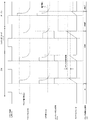
図12に、クランプ電圧設定に応じた分圧抵抗31,32の分圧比変更動作のタイミングチャートを示す。
クランプ電圧制御信号41Aが”00”のとき、クランプ電圧は、Vclamp1に設定されている。この時、スイッチ33A,34AがON、スイッチ33B、34BがONに設定される。これにより、ドライバ出力信号12Aは、分圧抵抗31により基準電圧信号58Aに対し、所定の電圧(Δv2)だけ低い電位に、分圧抵抗32により、基準電圧信号58Aに対し、所定の電圧(Δv2)だけ高い電位になるように分圧される。
クランプ電圧制御信号41Aが”01”のとき、クランプ電圧は、Vclamp2に設定されている。この時、スイッチ33A,34AがON、スイッチ33B、34BがOFFに設定される。これにより、ドライバ出力信号12Aは、分圧抵抗31により基準電圧信号58Aに対し、所定の電圧(Δv2)だけ低い電位に、分圧抵抗32により、基準電圧信号58Aに対し、所定の電圧(Δv2)だけ高い電位になるように分圧される。
クランプ電圧制御信号41Aが”10”のとき、クランプ電圧は、Vclamp3に設定されている。この時、スイッチ33A,34AがOFF、スイッチ33B、34BがOFFに設定される。これにより、ドライバ出力信号12Aは、分圧抵抗31により基準電圧信号58Aに対し、所定の電圧(Δv2)だけ低い電位に、分圧抵抗32により、基準電圧信号58Aに対し、所定の電圧(Δv2)だけ高い電位になるように分圧される。
このように、どのクランプ電圧設定においても、分圧後のクランプ電圧と基準電圧信号58Aとの電位差が一定になるように分圧比を制御することで、クランプ電圧に応じたクランプ電圧の診断が可能となる。
図13にクランプ電圧検出動作のタイミングチャートを示す。
始めに正常動作時の動作について説明する。
誘電性負荷10の通電停止により、逆起電圧が発生すると、電圧クランプ部20により、ドライバ出力12Aは所定のクランプ電圧にクランプされる。このドライバ出力信号12Aの電圧は分圧抵抗31,32により異なる分圧比で分圧され、コンパレータ51、52において、基準電圧信号58Aと比較される。正常動作時、分圧信号31Aと基準電圧信号58Aとの比較結果はロウレベル、分圧信号32Aと基準電圧信号58Aとの比較結果はハイレベルとなる。基準電圧信号58Aとの比較結果は、ドライバ駆動信号42Aの立下りのタイミングで生成された検知タイミング信号40Aにより、後段のフリップフロップ回路55,56に取り込まれ、クランプ電圧判定部57に入力される。クランプ電圧判定部57は、フリップフロップ回路55,56に格納されたコンパレータ51の出力がロウレベル、コンパレータ52の出力がハイレベルの場合は、正常と判定し、マイコン60に通知する。
次に、例えばクランプ部20内部のツェナーダイオード21Aがショート故障し、クランプ電圧が低電圧となった場合の動作について説明する。
誘電性負荷10の通電停止により、逆起電圧が発生すると、電圧クランプ部20により、ドライバ出力信号12Aは所定のクランプ電圧からショートしたツェナーダイオード21Aのツェナー電圧(Vz)分だけ低い電位にクランプされる。ドライバ出力信号12Aの電圧は分圧抵抗31,32により異なる分圧比で分圧され、コンパレータ51、52により基準電圧信号58Aと比較される。ツェナーダイオード21Aのショートによるクランプ電圧の低電圧異常発生時、分圧信号31A及び分圧信号32Aと基準電圧信号58Aとの比較結果はともにロウレベルが出力される。基準電圧信号58Aとの比較結果は、ドライバ駆動信号42Aの立下りのタイミングで生成された検知タイミング信号40Aにより、後段のフリップフロップ回路55,56に取り込まれ、クランプ電圧判定部57に入力される。クランプ電圧判定部57は、フリップフロップ回路55,56に格納されたコンパレータ51及び52の出力がともにロウレベルの場合は、低電圧異常と判定し、マイコン60に通知する。
最後に、例えばクランプ部20のツェナーダイオード21Aがオープン故障し、クランプ電圧が低電圧となった場合の動作について説明する。
誘電性負荷10の通電停止により、逆起電圧が発生すると、ドライバ出力信号12Aは、電圧クランプ部20によりクランプされないため、所定のクランプ電圧以上の電圧となる。
ドライバ出力信号12Aの電圧は分圧抵抗31,32により異なる分圧比で分圧され、コンパレータ51、52により基準電圧信号58Aと比較される。ツェナーダイオード21Aのオープンによるクランプ電圧の過電圧異常発生時、分圧信号31A及び32Aと基準電圧信号58Aとの比較結果はともにハイレベルが出力される。基準電圧信号58Aとの比較結果は、ドライバ駆動信号42Aの立下りのタイミングで生成された検知タイミング信号40Aにより、後段のフリップフロップ回路55,56に取り込まれ、クランプ電圧判定部57に入力される。クランプ電圧判定部57は、フリップフロップ回路55,56に格納されたコンパレータ51及び52の出力がともにハイレベルの場合は、過電圧異常と判定し、マイコン60に通知する。
このように、分圧比を調整可能な分圧抵抗31,32と基準電圧が入力された2つのコンパレータ51,52を備え、分圧抵抗によりそれぞれ異なる分圧比で分圧された分圧信号と基準電圧信号58Aを比較することで、第1の実施例と同様にクランプ電圧に応じた故障診断が可能となる。
また、本実施例では1つの電圧判定閾値と分圧抵抗により分圧された2つの分圧電位を比較することで、クランプ電圧の異常を検出しているが、3つ以上の電圧判定閾値とクランプ電圧の分圧電位を比較することでも同様の効果を期待できることは明白である。
図3は第3の実施例である誘導性負荷を駆動する電子制御装置の構成図である。
第1及び第2の実施例では、クランプ電圧の分圧電位を直接測定することでクランプ電圧異常の検出を行っているが、第3の実施例では、クランプ電圧と逆起電圧が発生する期間との間に相関があることを利用し、逆起電圧が所定の電圧閾値を上回った時間を測定することで、間接的にクランプ電圧異常の検出を行う点が異なる。
本実施例の電子制御装置は、バッテリー電源1に接続された誘導性負荷10と、前記誘導性負荷10の通電を制御するスイッチ素子12と、分圧抵抗30と、誘電性負荷10による逆起電圧を一定の電圧にクランプする電圧クランプ部20と、クランプ電圧異常を検出する電圧検出部50と逆起電圧が発生している期間を測定する時間測定部70により構成されている。
電圧検出部50と時間測定部70以外の機能については、第1の実施例と同様である。
以降の本実施例の説明で前述の第1の実施例と説明が重複する部分については省略する。
クランプ電圧検出部50は基準電圧信号58Aが入力されたコンパレータ51であり、ドライバ出力信号12Aの電圧を分圧抵抗30で分圧した分圧信号30Aと基準電圧信号58Aをコンパレータ51で比較し、分圧電位が基準電圧信号58Aを上回っている間、ハイレベルを出力する。
時間測定部70は、2つのタイマ(測定用タイマ71,期待値用タイマ72)と、タイマのカウント値の比較を行うカウンタ比較部73を備えており、電圧検出部50の出力がハイレベルとなっている期間をタイマで測定し、期待値範囲と比較することでクランプ電圧故障の検出を行う。
図14にクランプ電圧検出動作のタイミングチャートを示す。
バッテリー電圧1が投入されると、マイコンからの命令により学習モード信号60Aがハイレベルとなる。学習モード信号60Aがハイレベルの間、時間測定部70は、学習モードに入る。学習モード時に逆起電圧が発生し、ドライバ出力信号12Aを分圧抵抗30で分圧した分圧信号30Aの電位が基準電圧信号58A以上になると、電圧検出部50の出力がハイレベルとなる。電圧検出部50の出力がハイレベルとなると、期待値用タイマ72がカウントを開始する。その後、ドライバ出力信号12Aの電位が下がり、分圧信号30Aの電位が基準電圧信号58A以下になると、電圧検出部50の出力がロウレベルとなる。電圧検出部50の出力がロウレベルになると、期待値用タイマ72はカウントを停止し、カウント値を保持する。この時、保持された期待値用タイマ72のカウンタ値に基づき、逆起電圧発生時間の期待値範囲が算出される。
学習モード信号60Aがロウレベルとなると、判定モードに移行する。
判定モード時に、逆起電圧が発生し、ドライバ出力信号12Aを分圧抵抗30で分圧した分圧信号30Aの電位が基準電圧信号58A以上になると、電圧検出部50の出力はハイレベルとなる。電圧検出部50の出力がハイレベルになると、測定用タイマ71がカウントを開始する。その後、ドライバ出力信号12Aの電位が下がり、分圧信号30Aの電位が基準電圧信号58A以下になると、電圧検出部50の出力はロウレベルとなる。電圧検出部50の出力はロウレベルになると、測定用タイマ71はカウントを停止する。この時、カウンタ比較部73にて、測定用タイマ71のカウント値と学習モード時に算出された期待値範囲内との比較を行う。
測定用タイマ71のカウンタ値が期待値範囲に含まれる場合は正常、期待値範囲以下の場合は低電圧、期待値範囲以上の場合は過電圧を検出し、クランプ期間判定信号73Aをマイコン60に出力する。
本実施例によると、実施例1及び2のようにクランプ電圧を直接測定するのではなく、逆起電圧の分圧電位が所定の電圧を上回る時間を事前に測定し、最新の測定値と比較することにより、クランプ電圧故障の検出を行うこともできる。
本実施例は、分圧抵抗により分圧されたクランプ電圧と基準電圧生成部により生成された所定の電圧閾値を上回った時間をタイマで検出することによりクランプ電圧異常の検知を行っているが、基準電圧生成部58の代わりに可変電圧生成部を設け、クランプ電圧設定に応じて、電圧閾値を変更することで、特に、クランプ電圧を低電圧に設定した場合においてさらに安定した検知が期待できることは明白である。
また、本実施例は第2の効果として、以下の効果もある。
本実施例は、2つのタイマ(測定用タイマ71、期待値用タイマ72)を備え、期待値用タイマ72でクランプ電圧が所定の電圧を上回った時間を事前に測定し、その後、測定用タイマ71で同様に測定した時間と比較することでクランプ電圧の検出を行っている。
しかし、タイマが正常に動作していることが前提であり、どちらかのタイマが故障した場合は、クランプ電圧の異常検出が正常に行えないという問題があった。
本実施例では、この問題を解決するため、学習モード時に2つのタイマを同時に動作させ、カウント停止後2つのタイマのカウンタ値を確認することでタイマの故障を検出することができる。
図15にタイマの故障検出動作のタイミングチャートを示す。
学習モード時に逆起電圧が発生し、これにより分圧信号30Aの電位が基準電圧信号58A以上となり、電圧検出部50の出力がハイレベルとなると、期待値用タイマ72だけでなく、測定用タイマ71も同一のタイミングでカウントを開始する。その後、出力信号12Aの電位の減少に伴い、分圧信号30Aの電位が下がり、基準電圧信号58Aの電位を下回ると、電圧検出部50の出力がロウレベルとなる。電圧検出部50の出力がロウレベルになると、測定用タイマ71と期待値用タイマ72ともカウントを停止する。この時、クランプ期間判定部73にて、測定用タイマ71と期待値用タイマ72のカウント値を比較し、カウント値が著しく異なる場合は、いずれかのタイマが故障していると判断し、マイコン60に通知する。
このように、本実施例の第2の効果として、2つのタイマのカウント値を相互に監視することでタイマの故障検出を行うことができる。
図4は第4の実施例である誘導性負荷を駆動する電子制御装置の構成図である。
第4の実施例は、逆起電圧が所定の電圧閾値を上回っている時間を測定し、期待値範囲と比較することでクランプ電圧異常を行う点では第3の実施例と同一だが、期待値範囲の算出方法が第3の実施例とは異なる。
第3の実施例では、学習モード時に測定された1つの測定値から期待値範囲の算出を行うが、第4の実施例では、過去の負荷駆動時において測定された逆起電圧の発生時間をレジスタに保存しておき、保存された過去の測定値から期待値範囲の算出を行う点が異なる。
本実施例は第3の実施例と時間測定部70の構成のみが異なるため、それ以外の構成については説明を省略する。
なお、本実施例の説明で前述の第1の実施例と説明が重複する部分についても省略する。
時間測定部70は、タイマ74と、タイマのカウント値の比較を行うカウンタ比較部73と、タイマのカウント値を保存するレジスタ75を備えており、電圧検出部50の出力がハイレベルとなっている期間をタイマで測定し、レジスタに保存されたカウンタ値から算出された期待値範囲と比較することでクランプ電圧故障の検出を行う。
図16にクランプ電圧検出動作のタイミングチャートを示す。
バッテリー電圧1の投入後、ドライバ駆動信号42Aによりスイッチ素子12Aがオフされ、誘電性負荷10への通電が停止されると、逆起電圧が発生する。これにより、ドライバ出力信号12Aを分圧抵抗30で分圧した分圧信号30Aの電位が基準電圧信号58A以上となると、コンパレータ出力信号51Aはハイレベルとなる。コンパレータ出力信号51Aがハイレベルとなると、タイマ74がカウントを開始する。その後、ドライバ出力信号12Aの電位が減少し、分圧信号30Aの電位が基準電圧信号58A以下となり、コンパレータ出力信号51Aがロウレベルになると、タイマ74はカウントを停止し、カウンタ値をレジスタ75に保存する。レジスタ75には、所定の駆動回数分のカウンタ値が保存されている。カウンタ比較部73は、レジスタに格納されているカウンタ値から、期待値範囲を算出する。算出方法は、例えば、過去の駆動回数N回部の測定値の平均により算出する方法、過去の駆動回数N回分の測定値の中央値により算出する方法などが考えられる。カウンタ比較部73は、期待値範囲を算出し、最新のカウント値と比較する。最新のカウンタ値が期待値範囲に含まれる場合は正常、期待値範囲以下の場合は低電圧を、期待値範囲以上の場合は過電圧を検出し、クランプ期間判定信号73Aをマイコン60に出力する。
本実施例によれば、以前の駆動時に発生した逆記電圧発生時間を保存しておくレジスタを設けることで、第3の実施例のように事前に逆記電圧発生時間の学習を行わなくとも、第3の実施例と同様のクランプ電圧故障検出が可能である。
本実施例は、分圧抵抗により分圧されたクランプ電圧と基準電圧生成部により生成された所定の電圧閾値を上回った時間をタイマで検出することによりクランプ電圧異常の検知を行っているが、基準電圧生成部の代わりに可変電圧生成部を設け、クランプ電圧設定に応じて、電圧閾値を変更することで、特に、クランプ電圧を低電圧に設定した場合においてさらに安定した検知が期待できることは明白である。
なお、本発明は上記した実施例に限定されるものではなく、様々な変形例が含まれる。例えば、上記した実施例は本発明を分かりやすく説明するために詳細に説明したものであり、必ずしも説明した全ての構成を備えるものに限定されるものではない。また、ある実施例の構成の一部を他の実施例の構成に置き換えることが可能であり、また、ある実施例の構成に他の実施例の構成を加えることも可能である。また、各実施例の構成の一部について、他の構成の追加・削除・置換をすることが可能である。
また、信号線は説明上必要と考えられるのを示しており、製品上必要な全ての信号線を示しているとは限らない。
1 バッテリー電源
2 グランド電源
3 VCC電源
4 負荷抵抗
5 センスMOSトランジスタ
10 誘電性負荷
11 コンデンサ
12 スイッチ素子
12A ドライバ出力信号
13 シャント抵抗
13A 負荷電流
20 電圧クランプ部
21 ツェナーダイオード
22 ダイオード
23 ツェナーダイオード切替スイッチ
23A スイッチ23A
23B スイッチ23B
30 分圧抵抗1
31 分圧抵抗2
32 分圧抵抗3
33 分圧比切替スイッチ1
33A スイッチ33A
33B スイッチ33B
34 分圧比切替スイッチ2
34A スイッチ34A
34B スイッチ34B
40 検知タイミング制御部
41 クランプ電圧制御部
41A クランプ電圧制御信号
42 ドライバ駆動部
43 電流検出部
43A 判定結果マスク信号
44 パルス幅検出部
45 ANDゲート
46 ORゲート1
47 ORゲート2
50 電圧検出部
51 コンパレータ1
52 コンパレータ2
53 上側判定閾値生成部
54 下側判定閾値生成部
55 フリップフロップ回路1
55A フリップフロップ回路出力信号1
56 フリップフロップ回路2
56A フリップフロップ回路出力信号2
57 クランプ電圧判定部
57A クランプ電圧判定信号
58 基準電圧生成部
58A 基準電圧信号
60 マイコン
60A 学習信号
70 時間測定部
71 測定用タイマ
72 期待値用タイマ
73 カウンタ値比較部
73A クランプ期間判定信号
Claims (17)
- 電子負荷を駆動するスイッチ素子と、電子負荷への通電が停止されたときに生じる逆起電圧を一定電圧にクランプする電圧クランプ手段と、逆起電圧を所定の電圧と比較する電圧検出手段と、前記電圧検出手段の比較タイミングを制御する検知信号を生成する検知タイミング制御部とを備え、前記電圧検出手段により、所定の電圧と逆起電圧を比較することで、前記電圧クランプ手段の異常を検知することを特徴とする電子制御装置。
- 電子負荷を駆動するスイッチ素子と、電子負荷への通電が停止されたときに生じる逆起電圧を一定電圧にクランプする電圧クランプ手段と、逆起電圧が発生していることを検出する電圧検出手段と、逆起電圧が発生している時間を測定する時間測定手段を備え、所定の時間と時間測定手段により測定された逆記電圧の発生時間を比較することでクランプ電圧の異常を検知することを特徴とする電子制御装置。
- 電子負荷を駆動するスイッチ素子と、電子負荷への通電が停止されたときに生じる逆起電圧を一定電圧にクランプする電圧クランプ手段を備え、電圧クランプ手段は、クランプする電圧を変更するスイッチ手段を有することを特徴とする電子制御装置。
- 前記所定の電圧は、少なくとも2つの電圧判定閾値であって、逆起電圧を分圧する電圧分圧手段をさらに備え、分圧抵抗により分圧された分圧電位と少なくとも2つの電圧判定閾値を比較することで、前記電圧クランプ手段の異常を検知することを特徴とする請求項1に記載の電子制御装置。
- 前記少なくとも2つの電圧判定閾値から選定した2つの電圧判定閾値と前記分圧手段により分圧された分圧電位を比較し、クランプ電圧が選定した一方の電圧判定閾値以上、かつ、選定したもう一方の電圧判定閾値以下の場合は正常と検出し、選定した2つの電圧判定閾値より大きい場合には過電圧と検出し、選定した2つの電圧判定閾値より小さい場合には低電圧を検出することを特徴とする請求項4に記載の電子制御装置。
- 前記電圧分圧手段は異なる分圧比を有した少なくとも2つの分圧手段であって、前記分圧手段により分圧された少なくとも2つの分圧電位と所定の電圧を比較することで、前記電圧クランプ手段の異常を検知することを特徴とする請求項1に記載の電子制御装置。
- 前記少なくとも2つの分圧手段により分圧された分圧電位から選定した2つの分圧電位と所定の電圧を前記電圧検出手段により比較し、所定の電圧が選定した一方の分圧電位以上、かつ、選定したもう一方の分圧電位以下の場合は正常を検出し、選定した2つの分圧電位より大きい場合には過電圧を検出し、選定した2つの分圧電位より小さい場合には低電圧を検出することを特徴とする請求項6に記載の電子制御装置。
- 前記電圧クランプ手段によりクランプ電圧が変更された場合、前記電圧検出手段は変更されたクランプ電圧に応じて前記少なくとも2つの電圧判定閾値を変更することを特徴とする請求項3に記載の電子制御装置。
- 前記電圧クランプ手段によりクランプ電圧が変更された場合、前記電圧検出手段は変更されたクランプ電圧に応じて前記分圧手段の分圧比を変更することを特徴とする請求項3に記載の電子制御装置。
- 前記電圧クランプ部による電圧クランプ動作が行えない場合、前記電圧検出手段の出力により前記スイッチ素子をオンさせることを特徴とする請求項1に記載の電子制御装置。
- 前記電圧クランプ部による電圧クランプ動作が行えない場合、前記時間測定手段の出力により前記スイッチ素子をオンさせることを特徴とする請求項2に記載の電子制御装置。
- 前記スイッチ素子の駆動パルス幅を測定するパルス幅検出手段をさらに備え、前記スイッチ素子の駆動パルス幅が所定の時間より短い場合、前記電圧検出手段の判定結果をマスクすることを特徴とする請求項1に記載の電子制御装置。
- 前記電子負荷に流れる電流を測定する電流検出手段をさらに備え、前記電子負荷に流れる電流が所定の電流より少ない場合、前記電圧検出手段の判定結果をマスクすることを特徴とする請求項1に記載の電子制御装置。
- 前記検知タイミング制御部が生成する検知信号は、前記クランプ手段によりクランプ電圧が変更された場合に、変更されたクランプ電圧に応じて、検知信号のパルス幅を調整することを特徴とする請求項1に記載の電子制御装置。
- 前記時間測定手段は2つのタイマであり、1つ目のタイマにより事前に測定した逆起電圧の発生時間から算出された所定の時間と、2つ目のタイマにより測定された逆記電圧の発生時間を比較することで前記電圧クランプ手段の異常を検知することを特徴とする請求項2に記載の電子制御装置。
- 前記2つのタイマを同時に動作開始、停止させ、その後2つのタイマのカウント値を比較することでタイマの故障を検出することを特徴とする請求項15に記載の電子制御装置。
- 前記時間測定手段により測定された測定値を保存する保存手段をさらに備え、前記タイマにより測定された逆起電圧の発生時間と、保存手段に保存されている測定結果から算出された所定の時間とを比較することで前記電圧クランプ手段の異常を検知することを特徴とする請求項2に記載の電子制御装置。
Priority Applications (1)
| Application Number | Priority Date | Filing Date | Title |
|---|---|---|---|
| JP2015541561A JP6377067B2 (ja) | 2013-10-10 | 2014-10-06 | 電子制御装置 |
Applications Claiming Priority (2)
| Application Number | Priority Date | Filing Date | Title |
|---|---|---|---|
| JP2013-212437 | 2013-10-10 | ||
| JP2013212437 | 2013-10-10 |
Publications (1)
| Publication Number | Publication Date |
|---|---|
| WO2015053206A1 true WO2015053206A1 (ja) | 2015-04-16 |
Family
ID=52813022
Family Applications (1)
| Application Number | Title | Priority Date | Filing Date |
|---|---|---|---|
| PCT/JP2014/076650 Ceased WO2015053206A1 (ja) | 2013-10-10 | 2014-10-06 | 電子制御装置 |
Country Status (2)
| Country | Link |
|---|---|
| JP (1) | JP6377067B2 (ja) |
| WO (1) | WO2015053206A1 (ja) |
Cited By (9)
| Publication number | Priority date | Publication date | Assignee | Title |
|---|---|---|---|---|
| JP2017041813A (ja) * | 2015-08-21 | 2017-02-23 | 日立オートモティブシステムズ株式会社 | 電磁負荷駆動装置 |
| JP2017212600A (ja) * | 2016-05-25 | 2017-11-30 | 富士電機株式会社 | 異常検出装置 |
| JPWO2017130669A1 (ja) * | 2016-01-29 | 2018-08-16 | 日立オートモティブシステムズ株式会社 | 電磁負荷駆動装置、車載制御システム |
| JP2019036768A (ja) * | 2017-08-10 | 2019-03-07 | 日立オートモティブシステムズ株式会社 | 半導体装置および製造方法 |
| CN111769614A (zh) * | 2020-07-09 | 2020-10-13 | 昂宝电子(上海)有限公司 | 快充系统的检测电路及方法、快充协议电路和快充系统 |
| WO2021124644A1 (ja) * | 2019-12-20 | 2021-06-24 | 株式会社タムラ製作所 | ゲート駆動回路 |
| US20220170437A1 (en) * | 2019-04-26 | 2022-06-02 | Autonetworks Technologies, Ltd. | Control device |
| JP2024055589A (ja) * | 2022-10-07 | 2024-04-18 | 古河電気工業株式会社 | 保護装置 |
| US12007417B2 (en) | 2020-02-21 | 2024-06-11 | Signify Holding B.V. | Voltage sensing circuit and method |
Families Citing this family (1)
| Publication number | Priority date | Publication date | Assignee | Title |
|---|---|---|---|---|
| WO2020032213A1 (ja) * | 2018-08-09 | 2020-02-13 | 富士電機株式会社 | 半導体装置 |
Citations (3)
| Publication number | Priority date | Publication date | Assignee | Title |
|---|---|---|---|---|
| JPS62290111A (ja) * | 1986-06-09 | 1987-12-17 | Mitsubishi Electric Corp | 誘導性負荷駆動回路の故障検出回路 |
| JPH06252721A (ja) * | 1993-02-22 | 1994-09-09 | Toyota Autom Loom Works Ltd | 半導体スイッチの駆動回路 |
| JP2004247877A (ja) * | 2003-02-12 | 2004-09-02 | Denso Corp | 誘導性負荷駆動用ic、その使用方法及び電子装置 |
-
2014
- 2014-10-06 WO PCT/JP2014/076650 patent/WO2015053206A1/ja not_active Ceased
- 2014-10-06 JP JP2015541561A patent/JP6377067B2/ja not_active Expired - Fee Related
Patent Citations (3)
| Publication number | Priority date | Publication date | Assignee | Title |
|---|---|---|---|---|
| JPS62290111A (ja) * | 1986-06-09 | 1987-12-17 | Mitsubishi Electric Corp | 誘導性負荷駆動回路の故障検出回路 |
| JPH06252721A (ja) * | 1993-02-22 | 1994-09-09 | Toyota Autom Loom Works Ltd | 半導体スイッチの駆動回路 |
| JP2004247877A (ja) * | 2003-02-12 | 2004-09-02 | Denso Corp | 誘導性負荷駆動用ic、その使用方法及び電子装置 |
Cited By (13)
| Publication number | Priority date | Publication date | Assignee | Title |
|---|---|---|---|---|
| JP2017041813A (ja) * | 2015-08-21 | 2017-02-23 | 日立オートモティブシステムズ株式会社 | 電磁負荷駆動装置 |
| JPWO2017130669A1 (ja) * | 2016-01-29 | 2018-08-16 | 日立オートモティブシステムズ株式会社 | 電磁負荷駆動装置、車載制御システム |
| JP2017212600A (ja) * | 2016-05-25 | 2017-11-30 | 富士電機株式会社 | 異常検出装置 |
| JP2019036768A (ja) * | 2017-08-10 | 2019-03-07 | 日立オートモティブシステムズ株式会社 | 半導体装置および製造方法 |
| US11705806B2 (en) * | 2019-04-26 | 2023-07-18 | Autonetworks Technologies, Ltd. | Control device |
| US20220170437A1 (en) * | 2019-04-26 | 2022-06-02 | Autonetworks Technologies, Ltd. | Control device |
| WO2021124644A1 (ja) * | 2019-12-20 | 2021-06-24 | 株式会社タムラ製作所 | ゲート駆動回路 |
| JP2021100331A (ja) * | 2019-12-20 | 2021-07-01 | 株式会社タムラ製作所 | ゲート駆動回路 |
| JP7037538B2 (ja) | 2019-12-20 | 2022-03-16 | 株式会社タムラ製作所 | ゲート駆動回路 |
| US12007417B2 (en) | 2020-02-21 | 2024-06-11 | Signify Holding B.V. | Voltage sensing circuit and method |
| CN111769614A (zh) * | 2020-07-09 | 2020-10-13 | 昂宝电子(上海)有限公司 | 快充系统的检测电路及方法、快充协议电路和快充系统 |
| US12301126B2 (en) | 2020-07-09 | 2025-05-13 | On-Bright Electronics (Shanghai) Co., Ltd. | Systems and methods for detection and control related to charging |
| JP2024055589A (ja) * | 2022-10-07 | 2024-04-18 | 古河電気工業株式会社 | 保護装置 |
Also Published As
| Publication number | Publication date |
|---|---|
| JP6377067B2 (ja) | 2018-08-22 |
| JPWO2015053206A1 (ja) | 2017-03-09 |
Similar Documents
| Publication | Publication Date | Title |
|---|---|---|
| JP6377067B2 (ja) | 電子制御装置 | |
| KR101949509B1 (ko) | 모터 구동 ic 고장진단 장치 및 방법 | |
| US11708801B2 (en) | Load drive device, engine system | |
| US11223195B2 (en) | Control device and method for power supply to EPS in vehicle | |
| CN105939896A (zh) | 负载驱动电路 | |
| US7280333B2 (en) | Method and device for short circuit or open load detection | |
| US11867748B2 (en) | Electrical control device detection circuit, detection method, and electric vehicle | |
| KR102100861B1 (ko) | 로우 사이드 구동 ic 고장진단 장치 및 방법 | |
| CN100403035C (zh) | 电路系统和一种电路的检验方法 | |
| CN104011373B (zh) | 用于检查供电电路的方法以及用于至少一个点火电路的所属的供电电路 | |
| US8698353B2 (en) | Method for operating a redundant system and system therefor | |
| JP5506958B2 (ja) | 電流回路を作動するためのエンジン制御装置およびエンジン制御方法 | |
| JP3990669B2 (ja) | 負荷の故障診断方法及び装置並びに負荷の故障処理方法及び装置 | |
| US10215795B1 (en) | Three level gate monitoring | |
| US10770886B2 (en) | Electromagnetic load drive device and in-vehicle control system | |
| EP3627686A1 (en) | Motor drive device | |
| KR102046350B1 (ko) | 승객 보호 수단을 위한 집적 조정기, 특히 전압 조정기 및 제어 장치 | |
| CN104349943B (zh) | 用于具有可配置的输出电压的人员保护设备的集成的控制器,尤其是电压控制器以及控制装置 | |
| KR100587923B1 (ko) | 전자제어유닛의 센서 전원 제어 회로 | |
| KR101776475B1 (ko) | 엑추에이터 회로 고장 진단 장치 및 방법 | |
| WO2020059351A1 (ja) | 電子制御装置 | |
| KR20200069677A (ko) | 경고등 구동 장치 및 경고등 구동 방법 | |
| KR20180029520A (ko) | 점화 코일 단락 검출 장치, 방법 및 이를 구비한 점화 코일 구동 시스템 및 방법 | |
| CN116455257A (zh) | 用于控制h桥逆变器系统的方法及电子设备 | |
| JP2015144352A (ja) | 負荷駆動装置 |
Legal Events
| Date | Code | Title | Description |
|---|---|---|---|
| 121 | Ep: the epo has been informed by wipo that ep was designated in this application |
Ref document number: 14852839 Country of ref document: EP Kind code of ref document: A1 |
|
| ENP | Entry into the national phase |
Ref document number: 2015541561 Country of ref document: JP Kind code of ref document: A |
|
| NENP | Non-entry into the national phase |
Ref country code: DE |
|
| 122 | Ep: pct application non-entry in european phase |
Ref document number: 14852839 Country of ref document: EP Kind code of ref document: A1 |