WO2015050225A1 - Biomolecule measuring device - Google Patents

Biomolecule measuring device Download PDF

Info

Publication number
WO2015050225A1
WO2015050225A1 PCT/JP2014/076446 JP2014076446W WO2015050225A1 WO 2015050225 A1 WO2015050225 A1 WO 2015050225A1 JP 2014076446 W JP2014076446 W JP 2014076446W WO 2015050225 A1 WO2015050225 A1 WO 2015050225A1
Authority
WO
WIPO (PCT)
Prior art keywords
mosfet
isfet
biomolecule
measuring device
cell
Prior art date
Application number
PCT/JP2014/076446
Other languages
French (fr)
Japanese (ja)
Inventor
河原 尊之
善光 柳川
板橋 直志
竹村 理一郎
Original Assignee
株式会社日立ハイテクノロジーズ
Priority date (The priority date is an assumption and is not a legal conclusion. Google has not performed a legal analysis and makes no representation as to the accuracy of the date listed.)
Filing date
Publication date
Application filed by 株式会社日立ハイテクノロジーズ filed Critical 株式会社日立ハイテクノロジーズ
Priority to US15/026,657 priority Critical patent/US10481125B2/en
Priority to CN201480054573.0A priority patent/CN105593675B/en
Priority to GB1605558.4A priority patent/GB2534318B/en
Publication of WO2015050225A1 publication Critical patent/WO2015050225A1/en

Links

Images

Classifications

    • GPHYSICS
    • G01MEASURING; TESTING
    • G01NINVESTIGATING OR ANALYSING MATERIALS BY DETERMINING THEIR CHEMICAL OR PHYSICAL PROPERTIES
    • G01N27/00Investigating or analysing materials by the use of electric, electrochemical, or magnetic means
    • G01N27/26Investigating or analysing materials by the use of electric, electrochemical, or magnetic means by investigating electrochemical variables; by using electrolysis or electrophoresis
    • G01N27/403Cells and electrode assemblies
    • G01N27/414Ion-sensitive or chemical field-effect transistors, i.e. ISFETS or CHEMFETS
    • G01N27/4145Ion-sensitive or chemical field-effect transistors, i.e. ISFETS or CHEMFETS specially adapted for biomolecules, e.g. gate electrode with immobilised receptors
    • GPHYSICS
    • G01MEASURING; TESTING
    • G01NINVESTIGATING OR ANALYSING MATERIALS BY DETERMINING THEIR CHEMICAL OR PHYSICAL PROPERTIES
    • G01N27/00Investigating or analysing materials by the use of electric, electrochemical, or magnetic means
    • G01N27/26Investigating or analysing materials by the use of electric, electrochemical, or magnetic means by investigating electrochemical variables; by using electrolysis or electrophoresis
    • G01N27/403Cells and electrode assemblies
    • G01N27/414Ion-sensitive or chemical field-effect transistors, i.e. ISFETS or CHEMFETS
    • G01N27/4148Integrated circuits therefor, e.g. fabricated by CMOS processing

Definitions

  • the present invention relates to a biomolecule measuring apparatus, and more particularly to a biomolecule measuring apparatus using semiconductor technology.
  • Patent Document 1 describes a DNA sequencer that determines the base sequence of deoxyribonucleic acid (DNA) at low cost and at high speed using a pH sensor array (semiconductor sensor) manufactured by semiconductor technology.
  • the semiconductor sensor can quantify the reaction between the target biomolecule sample and the reagent based on the strength of the electric signal. Therefore, an expensive fluorescent reagent as in the prior art is unnecessary, which is advantageous in terms of cost.
  • millions to hundreds of millions of sensors can be integrated on a single semiconductor substrate by a semiconductor microfabrication technique, and measurement can be performed in parallel, so that measurement throughput is easily improved.
  • ISFET ion-sensitive field effect transistor
  • Patent Document 1 a change in hydrogen ion concentration generated by a DNA elongation reaction by a reagent is measured by using an ISFET.
  • the type of base can be specified from changes in the hydrogen ion concentration.
  • the four types of bases are adenine, thymine, cytosine, and guanine.
  • the theoretical voltage change due to the change in hydrogen ion concentration can theoretically be obtained from an equation called the Nernst equation.
  • the voltage change is approximately 59 mV / pH.
  • This change fluctuation
  • the gate voltage of the ISFET changes the gate voltage of the ISFET, and the output current of the ISFET changes.
  • the voltage fluctuation with respect to the fluctuation of the hydrogen ion concentration is lower than the theoretical value, and is about several tens mV per pH.
  • the change in the hydrogen ion concentration generated by the DNA elongation reaction depends on the number of DNA strands causing the reaction, the size of the space causing the reaction, and the reagent, but it is about 0.1 mV when the pH changes. For this reason, the change in the output signal of the ISFET is extremely small.
  • Patent Document 2 a large number of ISFETs are arranged in an array, and in FIG. 75F, a unit cell for detecting a change in the concentration of hydrogen ions is shown as 75F1.
  • the unit cell 75F1 has a function of increasing sensitivity.
  • the portion shown as ISFET is a circuit representation of ISFET, and the ISFET is composed of an ion sensitive film (portion) 75F6 and a MOSFET (transistor) 75F2 connected to the gate.
  • 75F3 is a MOSFET for applying a bias current
  • 75F4 is a MOSFET for connecting to an output signal line 75F7 (Column Bus).
  • Row Select is a signal line for selecting the unit cell 75F1.
  • the sensitivity of the ISFET is increased by the MOSFET 75F5. That is, the output of the MOSFET 75F2 is input to the gate of the MOSFET 75F5.
  • the gate voltage of the ISFET formed by the MOSFET 75F2 and the ion sensitive film 75F6 is changed by the change of the hydrogen ion concentration. Due to this change, the output current of the ISFET changes.
  • This change is once amplified by the MOSFET 75F5. That is, a small change in ISFET output current due to a change in hydrogen ion concentration is amplified. After being amplified, it is output to the output signal line 75F7 via the MOSFET 75F4. As a result, the sensitivity of the ISFET is increased.
  • Non-Patent Document 1 describes that charges are accumulated particularly in an ion sensitive film, a protective film, an electrode interface, a floating electrode, and a gate oxide film.
  • Non-Patent Document 1 describes that the threshold voltage of the ISFET is offset by about ⁇ 10 V due to such charge accumulation.
  • Patent Document 1 discloses a method of applying energy to a charge by irradiating ultraviolet rays and extracting the charge to the outside of the device. Further, it is described in Non-Patent Document 2 that irradiation with ultraviolet rays needs to be performed for a long time, for example, 10 hours. As another method, Non-Patent Document 3 describes that a change in threshold voltage due to trapped charges can be reduced by hot electron injection.
  • Non-Patent Document 3 discusses hot electron injection into a single ISFET with respect to a method for reducing offset. However, no investigation has been made on a method particularly suitable for a biomolecule measuring apparatus in which a plurality of ISFETs are arranged in an array.
  • An object of the present invention is to provide a highly sensitive biomolecule measuring device having a plurality of ISFETs.
  • the biomolecule measuring apparatus is provided with a semiconductor sensor that detects ions generated by the reaction between the biomolecule sample and the reagent.
  • the semiconductor sensor is arranged in an array on a semiconductor substrate, and has a plurality of cells each detecting ions and a plurality of readout lines arranged in the array.
  • Each of the plurality of cells arranged in an array has a floating gate, an ISFET that detects a change in the concentration of ions, a gate that receives the output of the ISFET, and a first MOSFET that amplifies the output of the ISFET And a second MOSFET for selectively transmitting the output of the first MOSFET to a corresponding readout line of the plurality of readout lines.
  • each of the plurality of cells includes a third MOSFET that is connected to the ISFET, generates hot electrons (hot carriers) in the ISFET, and injects charges into the floating gate of the ISFET.
  • the second MOSFET and the third MOSFET can be controlled separately.
  • the output of the ISFET amplified by the first MOSFET can be read.
  • the third MOSFET is controlled based on the read output.
  • hot electrons hot carriers
  • the threshold voltage of the ISFET can be set based on the read output. In this way, by setting the threshold voltage of the ISFET in each of a plurality of cells arranged in an array, fluctuations in the threshold voltage caused by charges accumulated during manufacturing or the like can be reduced. It becomes possible to reduce between ISFETs, and a highly sensitive biomolecule measuring device can be obtained.
  • the biomolecule measuring device has a first operation mode in which a tunnel current flows from the floating gate of the ISFET in each of the plurality of cells to the semiconductor substrate.
  • the threshold voltage of each of the plurality of ISFETs changes in a predetermined direction (high direction or low direction).
  • the threshold voltages of a plurality of ISFETs can be made uniform.
  • the biomolecule measuring device controls the third MOSFET to inject charges into the floating gate of the ISFET, and controls the second MOSFET to output the ISFET.
  • the operation is alternately performed to determine whether or not the threshold voltage of the ISFET is within a predetermined range, and the threshold voltage of the ISFET in each of the plurality of cells is within the predetermined range. Make it fit.
  • the first operation mode described above is executed before the operation of injecting charges into the floating gate of the ISFET.
  • the threshold voltages of the respective ISFETs are controlled so as to be within a predetermined range. It becomes possible to keep the threshold voltage of the ISFET within a predetermined range.
  • a highly sensitive biomolecule measuring apparatus can be provided.
  • FIG. 3 is a circuit diagram showing a configuration of a cell according to the first embodiment.
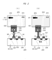
  • (A) And (B) is a schematic diagram for demonstrating the mechanism which cancels offset.
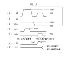
  • (A) to (G) are waveform diagrams showing the operation of the first embodiment.
  • (A) to (E) are waveform diagrams showing other operations of the first embodiment.
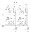
  • FIG. 6 is a circuit diagram illustrating a configuration of a semiconductor sensor according to a second embodiment. It is a block diagram which shows the structure of a biomolecule measuring device. It is a typical sectional view of a semiconductor sensor. It is sectional drawing of a semiconductor sensor. It is a top view of a semiconductor sensor. It is a top view of a semiconductor sensor. It is a top view of a semiconductor sensor. It is a top view of a semiconductor sensor.
  • FIG. 6 is a circuit diagram of a semiconductor sensor according to Embodiment 3.
  • FIG. FIG. 6 is a circuit diagram showing a circuit of a semiconductor sensor according to a fourth embodiment.
  • FIG. 9 is a schematic cross-sectional view of a semiconductor sensor according to a fifth embodiment. It is a block diagram which shows the structure of a biomolecule measuring device.
  • A) And (B) is a wave form diagram explaining operation
  • FIG. 10 is a circuit diagram illustrating a configuration of a cell according to a sixth embodiment. It is a circuit diagram which shows the structure of a cell.
  • FIG. 10 is a circuit diagram showing a configuration of a semiconductor sensor according to a seventh embodiment.
  • (A) And (B) is a figure which shows the function of the data processing part of a biomolecule measuring device. It is a figure which shows the structure of the data processing part of a biomolecule measuring device.
  • Semiconductor sensors are manufactured on a single semiconductor substrate using semiconductor technology. That is, the semiconductor sensor has a plurality of cells formed in one semiconductor substrate by semiconductor technology and arranged in an array on the semiconductor substrate.
  • a semiconductor sensor is installed in the biomolecule measuring apparatus, which will be described later with reference to FIG.
  • each of a plurality of cells arranged in an array includes an ISFET and an amplifying transistor in order to increase the sensitivity of the cell, and further reduces the offset of the ISFET. And a signal line necessary for this operation.
  • an N-channel field effect transistor (MOSFET) formed on a semiconductor substrate is used as a transistor.
  • MOSFET N-channel field effect transistor
  • FIG. 1 is a circuit diagram showing a configuration of a cell according to the present embodiment. The figure shows the configuration of one cell C11 among a plurality of cells arranged in an array. The plurality of cells arranged in an array have the same configuration.
  • each of M1 to M3 is a MOSFET.
  • the cell C11 includes an ISFET, a first MOSFET M2, a second MOSFET M3, and a third MOSFET M1.
  • the ISFET has a MOSFET MS having a floating gate and an ion sensitive film 100.
  • An example of the device structure of the ISFET will be described later with reference to FIGS. 2A and 2B, and the ion sensitive film 100 of the ISFET is immersed in a solution.
  • the MOSFET MS provided in the ISFET operates as a MOSFET having a floating gate.
  • a voltage corresponding to the operation is applied as a bias voltage VBias to the drain electrode (terminal) of the MOSFETMS, and the source electrode (terminal) of the MOSFETMS is connected to the node N1.
  • a control voltage VB is applied as a back bias voltage to the back gate (in this example, a semiconductor substrate) of the MOSFET MS.
  • the control voltage VB may be independent from or common to the back bias voltage applied to the back gates of the other MOSFETs M1 to M3 in the cell C11.
  • FIG. 1 shows an example in which the control voltage VB is also applied to the back gate of the MOSFET M1.
  • semiconductor regions having different electrical polarities are provided in order to be electrically insulated from other MOSFETs.
  • the node N1 to which the source electrode of MOSFETMS is connected is connected to MOSFETs M1 and M2.
  • This configuration has one feature of the present embodiment. That is, the source electrode (node N1) of the MOSFET MS in the ISFET is connected to the drain electrode of the third MOSFET M1.
  • the gate of the third MOSFET M1 is connected to the offset cancel signal line WC1, and is driven by the offset cancel signal line WC1.
  • the offset of the MOSFET MS in the ISFET can be reduced.
  • the offset of the MOSFET MS in the ISFET in other words, the offset of the ISFET is caused by, for example, electric charges accumulated during manufacturing. Since the amount of stored charge varies depending on the position of the semiconductor substrate, the threshold voltage of MOSFETMS appears different for each cell arranged in an array.
  • the threshold voltage of each MOSFETMS (ISFET) to the same value by adjusting this. That is, it is possible to give different amounts of change to the threshold voltage for each cell.
  • the control voltage VB applied to the back gate of the MOSFETMS in the ISFET is set to a predetermined value, and a negative voltage is applied as the control voltage VR to the solution in which the ion sensitive film 100 is immersed, thereby making the MOSFET M1 It is also possible to change the direction of the threshold voltage applied to the MOSFET MS in the opposite direction.
  • the source electrode (node N1) of the MOSFET MS is also connected to the gate of the first MOSFET M2.
  • One electrode (source electrode or drain electrode) of the MOSFET M2 has a gate connected to the read signal line WR1, and is connected to the read line R1 via the second MOSFET M3 controlled by the read signal line WR1.
  • the signal change detected by the ion sensitive film 100 connected to the MOSFET MS is amplified by the MOSFET M2.
  • the amplified signal is selectively transmitted to the readout line by the MOSFET M3. This selective transmission operation is controlled independently of the MOSFET M1 by the read signal line WR1.
  • the operation for changing the threshold voltage of the MOSFETMS (ISFET) by the MOSFET M1 and the transmission operation can be controlled independently.
  • the signal from the MOSFETMS can be amplified, but the MOSFETMS signal itself has an offset, so that it is difficult to extract the signal detected by the ion sensitive film with high sensitivity. It was.
  • the read line R1 is connected to one input of the sense amplifier SA.
  • the sense amplifier SA amplifies the voltage difference between the reference voltage Vref applied to the other input and the read line R1 connected to one input, and outputs the result to OUT.
  • MOSFET M2 the other electrode (drain electrode or source electrode) of MOSFET M2 is connected to power supply voltage Vd, and one electrode (source electrode or drain electrode) of MOSFET M2 is connected to the other electrode of MOSFET M3. It is connected to an electrode (drain electrode or source electrode).
  • One electrode (source electrode or drain electrode) of the MOSFET M3 is connected to the corresponding readout line R1.
  • the MOSFETs M2 and M3 are connected in series between the power supply voltage Vd and the readout line R1.
  • MOSFET M1 is connected to the source electrode (node N1) of MOSFET MS, and one electrode (source electrode or drain electrode) of MOSFET M1 is connected to the ground voltage Vs of the circuit. ing.
  • MOSFET MS ISFET
  • MOSFET M1 MOSFET MS and the MOSFET M1 are connected in series between the bias voltage VBias and the circuit ground voltage Vs. Since the MOSFET M1 is connected in series with the MOSFET MS in the ISFET, when the MOSFET M1 is turned on, the source electrode (node N1) of the MOSFET MS becomes the ground voltage Vs of the circuit. Thereby, MOSFERTMS can form a channel through which a current flows between the bias voltage VBias and the node N1.
  • each cell including ISFETs arranged in an array can be realized.
  • FIG. 2 are schematic diagrams for explaining a mechanism for canceling an offset. That is, (A) and (B) of FIG. 2 show that the threshold voltage of MOSFETMS is changed by MOSFETMS, M1 and a signal line necessary to operate them. 2A and 2B show schematic cross sections of MOSFETMS and MOSFETM1 among the elements constituting the cell C11 shown in FIG. In FIGS. 2A and 2B, the structures of the MOSFETs MS and M1 shown are the same.
  • the ISFET has a MOSFET MS and an ion sensitive film 100 connected thereto.
  • the sensitive film 100 is connected to the floating gate 203 of the MOSFET MS through the insulating film 209.
  • reference numeral 200 denotes a flow cell installed on the semiconductor sensor.
  • the flow cell 200 is filled with the solution 201.
  • the solution 201 is, for example, a solution in which a biomolecule sample and a reagent are mixed.
  • the flow cell 200 is provided with a reference electrode 202, and a reference control voltage VR is applied to the reference electrode 202.
  • MOSFET MS has a semiconductor region 205 that forms a source region corresponding to one electrode, and a semiconductor region 204 that forms a drain region corresponding to the other electrode. It is formed on the substrate 208. Further, the gate electrode of the MOSFET MS is disposed above the semiconductor substrate 208 and between the semiconductor regions 204 and 205 described above.
  • the MOSFET M1 is arranged so as to be connected in series with the MOSFET MS.
  • the semiconductor region 205 formed in the semiconductor substrate 208 is a semiconductor region (drain region) corresponding to the other electrode, and the semiconductor region 206 also formed in the semiconductor substrate 208 is , A semiconductor region (source region) corresponding to one of the electrodes.
  • the MOSFET M1 has a gate electrode which is disposed on the upper side of the semiconductor substrate 208 and between the semiconductor regions 205 and 206.
  • the semiconductor region 205 functions as a source region of the MOSFET MS and a drain region of the MOSFET M1.
  • the MOSFET MS and the semiconductor substrate 208 of M1 are common, and this semiconductor substrate 208 also functions as a back gate of the MOSFET MS and M1, and the bias voltage VB is applied.
  • the MOSFETs M2 and M3 described above are also formed on the semiconductor substrate 208 in the same manner as the MOSFET M1 described above.
  • the semiconductor substrate 208 is a P-type semiconductor
  • the semiconductor regions 204 to 206 are N-type semiconductors.
  • source / drain varies depending on the potential, it should be understood that the expression “source / drain” is an example in this specification.
  • the circuit ground voltage Vs (0 V) is applied to the semiconductor substrate 208 as the control voltage VB.
  • a negative voltage for example, ⁇ 5 V
  • a circuit ground voltage Vs (0 V) is applied to the sources (source electrodes) and drains (drain electrodes) of the MOSFETs MS and M1 and the gate of the MOSFET M1.
  • the solution 201 in the flow cell 200 becomes a negative potential due to the negative control voltage VR applied to the reference electrode 202.
  • the ground voltage Vs is applied to the semiconductor substrate 208, the potential of the semiconductor substrate 208 becomes higher than the potential of the solution 201 in the flow cell 200. As a result, a potential difference is generated between the floating electrode 203 of the MOSFET MS and the semiconductor substrate 208 so that the negative charge accumulated in the floating gate 203 is drawn toward the semiconductor substrate 208 side.
  • the negative charge accumulated in the floating electrode 203 is extracted to the semiconductor substrate 208 side.
  • a tunnel current flows, so that negative charges are extracted to the semiconductor substrate 208 as the tunnel current.
  • the control voltage VB is set to, for example, the circuit ground voltage Vs (0 V), and the control voltage VR is set to a desired positive voltage, for example.
  • 5 V is applied to the drain of the MOSFET MS (bias voltage VBias in FIG. 1), and a similar voltage (5 V) is also applied to the gate of the MOSFET M1.
  • the source of the MOSFET M1 is set to the ground voltage Vs (0 V), for example.
  • the threshold voltage of the MOSFET MS can be changed in a desired direction by the MOSFET MS, M1 and the signal line necessary to operate them. That is, it becomes possible to cancel the offset of the MOSFET MS caused by the charge accumulation.
  • 3A to 3G are operation waveform diagrams when the operation shown in FIG. 2B is performed in the configuration of the cell C11 shown in FIG.
  • the horizontal axis indicates time.
  • the vertical axis indicates the voltage.
  • a solution having an appropriate pH for adjustment is used as the solution 201 (FIG. 2B).
  • a solvent used for dissolving a cleaning solution or an enzyme used in an actual measurement operation may be used.
  • the magnitude of the change in threshold voltage of MOSFETMS can be changed for each cell.
  • the MOSFET MS of each cell has a different threshold voltage, that is, an offset due to charge accumulation at the time of manufacture, for example, or becomes different while continuing operation, the same threshold value is obtained. It becomes possible to match the voltage.
  • signals as a highly sensitive array can be obtained from a plurality of cells each including an ISFET and having an amplification function.
  • the temperature of the reagent can be changed in one measurement process. By changing the threshold voltage before changing the temperature, the signal after changing the temperature can be obtained with higher sensitivity.
  • a desired signal voltage VRW is applied to the control voltage VR. That is, the value of the control voltage VR is set to VRW.
  • a signal voltage VCM (5 V in FIG. 2B) is applied to the offset cancel signal line WC1 connected to the gate of the MOSFET M1.
  • the voltage VBW (5 V in FIG. 2B) is applied to the bias voltage VBias.
  • MOSFETMS and M1 are turned on.
  • the threshold voltage of the MOSFET MS is changed during the period “MS: threshold change” in FIG. 3, that is, the period during which the offset cancel signal line WC1 is at the high level (VCM). Is done.
  • the ISFET (MOSFETMS) signal is read.
  • VRR and VBR signal voltages are applied to the control voltage VR and the bias voltage VBias, respectively.
  • the voltage values of the signal voltages VRR and VBR are set to values lower than the voltages VRW and VBW described above.
  • MOSFETs M2 and M3 are operated here.
  • the signal voltage VRM is applied to the read signal line WR1 that controls the MOSFET M3.
  • a signal corresponding to the state of the threshold value of the MOSFET MS at this time is read (transmitted) to the read line R1.
  • the sense amplifier SA compares the voltage of the read line R1 with a predetermined reference voltage Vref, determines whether or not the voltage falls within a predetermined range, and outputs the result to OUT. This is referred to as a verify operation in the present specification.
  • the threshold voltage of the MOSFETMS (ISFET) is assumed to be within the predetermined range.
  • the threshold voltage of the MOSFET MS (ISFET) is not within the predetermined range. If the threshold voltage of MOSFETMS (ISFET) is within a predetermined range, the operation of changing the threshold voltage of MOSFETMS is terminated without being performed. On the other hand, when it is determined that the threshold voltage of MOSFETMS is not within the predetermined range, the operation in the “MS: threshold change” period shown in FIG. 3 is repeated.
  • an operation for changing the threshold value and a verify operation for reading the threshold value of the MOSFET MS (operation in the “MS: threshold verify” period in FIG. 3) are performed. Run one or more times alternately.
  • the threshold verify operation it is determined whether or not the threshold changing operation and the threshold verify operation are repeated according to whether or not the threshold voltage of the ISFET is within a predetermined range.
  • the offset cancel signal line WC1 is at the low level during the “MS: threshold verify” period. During this period, a predetermined signal voltage is applied to the offset cancel signal line WC1. May be applied. By doing so, a bias current flows through the MOSFET M1 during this period, and an optimum voltage can be generated at the node N1 (FIG. 1).
  • FIG. 3G as an example of the output OUT of the sense amplifier SA, the case where the threshold voltage of the MOSFET MS is changed and the case where no change is required are “MS: re-application required” and “MS: change It is shown as “End”.
  • FIG. 4A to 4E are waveform diagrams when the operation (first operation mode) described in FIG. 2A is performed in the cell C11 shown in FIG.
  • a control voltage VR having a signal voltage VRT that is a negative voltage is applied to the reference electrode 202 as its voltage value.
  • VRT signal voltage
  • the control voltage VB applied to the semiconductor substrate 208 is at a low level.
  • the operation period is set to a high level. Good.
  • the operation shown in FIG. 4 ((A) of FIG. 2) is performed, for example, on a plurality of cells arranged in an array before the operation of FIG. It is desirable to move the threshold voltage greatly in one direction. If the operation shown in FIG. 3 is performed after the operation shown in FIG. 4 is performed, the threshold voltage of each cell is changed in a direction opposite to this direction after the threshold voltage is moved collectively. The value can be changed by a required value. As a result, even if the threshold voltages of the ISFETs of the cells arranged in an array are different in a wide range, it is possible to make the values almost the same.
  • Each of the control voltage VB shown in FIG. 3B and the bias voltage VBias shown in FIG. 4 is, for example, the ground voltage Vs. (Embodiment 2)
  • FIG. 5 is a circuit diagram showing a configuration of the semiconductor sensor according to the second embodiment.
  • the semiconductor sensor has a plurality of cells arranged in an array.
  • cells in two rows and two columns among a plurality of cells arranged in an array are shown as representatives.
  • signal lines WR1, WR2, WC1, WC2 and read lines R1, R2 arranged in the array are also shown in the figure.
  • C11, C12, C21, and C22 are cells arranged in two rows and two columns in the array.
  • the cells C11, C12, C21, and C22 have the same configuration, and each configuration has the same configuration as the cell C11 described in FIG.
  • a plurality of signal wirings WR1, WR2, WC1, and WC2 and readout lines R1 and R2 are arranged.
  • a plurality of cells arranged in an array a plurality of cells C11 and C12 (C21 and C22) arranged in the same row include a read signal line WR1 corresponding to the row among the plurality of signal lines, and an offset.
  • Cancel signal lines WC1 (WR2, WC2) are connected.
  • the plurality of cells C11 and C21 (C12 and C22) arranged in the same column include the readout line R1 (R2) corresponding to the column among the plurality of readout lines. ) Is connected.
  • Corresponding sense amplifiers SA1 and SA2 are connected to the read lines R1 and R2. The connection between each cell and the signal line and readout line is the same as in FIG.
  • the operation for changing the threshold voltage of the MOSFETMS in each of the cells C11, C12, C21, and C22 is the same as the operation described above with reference to FIGS.
  • the operation shown in FIG. 4 is collectively performed on the plurality of cells C11, C12, C21, and C22 constituting the array.
  • the threshold voltage of MOSFETMS in each of the cells moves in one direction.
  • the operation shown in FIG. 3 is performed for each row of the array. That is, in FIG. 5, the operation shown in FIG. 3 is performed on the cells C11 and C12 (C21 and C22) arranged in the same row.
  • the cell threshold voltage is controlled to a desired value in units of rows. In this case, it is conceivable that the amount of charge accumulated in the floating gate 203 of the MOSFET MS is different even in cells arranged in the same row.
  • the number of repetitions in which the operation shown in FIG. 3 is performed may change between cells arranged in the same row.
  • the sense amplifier SA is different for each column, the operation shown in FIG. 3 can be performed in units of rows as described above, and the operation for keeping the threshold voltage within a predetermined range can be accelerated. It becomes.
  • the threshold voltages of the ISFETs (MOSFETMS) of each cell can be made substantially equal, and the amplification MOSFET M2 provided in each cell can achieve high sensitivity. A signal can be acquired.
  • the biomolecules are measured after the threshold voltage of the MOSFETMS of each cell falls within a predetermined range. That is, the change in the hydrogen ion concentration generated by the DNA elongation reaction by the reagent is detected by a plurality of cells arranged in the array.
  • the outputs OUT1 and OUT2 of the sense amplifiers SA1 and SA2 are signals indicating changes in the hydrogen ion concentration. Therefore, it is possible to measure the change in the hydrogen in concentration in parallel in a plurality of cells (row units). Of course, an operation of changing the threshold voltage may be performed during the measurement. ⁇ Configuration of biomolecule measuring device>
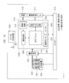
  • FIG. 6 is a block diagram showing the overall configuration of the biomolecule measuring apparatus.
  • the biomolecule sample to be measured is actually attached to the beads as will be described later, and filled in the flow cell 200 (FIGS. 2A and 2B) loaded on the semiconductor sensor (ISFET array chip) 1002. Is done.
  • the semiconductor sensor (ISFET array chip) 1002 includes an ISFET array 304, a selection circuit 305, a readout circuit 309, and a control circuit 315, which are formed on one semiconductor substrate by semiconductor technology.
  • the ISFET array 304 has the array described in FIG.
  • the selection circuit 305 selects the plurality of cells from the ISFET array 304 by controlling the voltages of the read signal lines WR1 and WR2 and the offset cancel signal lines WC1 and WC2. For example, the read signal line WR1 is set to the high level, the remaining read signal lines WR2 are set to the low level, and the plurality of cells C11 and C12 connected to the read signal line WR1 are selected. A signal from the selected cell is transmitted to the readout circuit 309 through readout lines R1 and R2.
  • the control circuit 315 receives the output from the readout circuit 309 and controls the selection circuit 305 and the VR / VB formation circuit 600 in order to perform the operation described with reference to FIGS.
  • the control circuit 315 instructs the selection circuit 305 to sequentially select the offset cancel signal lines WC1 and WC2 in the ISFET array 304, for example.
  • the control voltages VB and VR and the bias voltage VBias as shown in FIG. 3 are formed so as to change the threshold voltage of the MOSFETMS in the selected cell, and the reference electrode 202, the semiconductor substrate 208 and each cell are formed.
  • the bias voltage VBias supplied from the VR / VB forming circuit 600 to the ISFET array 304 is not shown in order to avoid complication of the drawing, but in this embodiment, the bias voltage is not shown.
  • VBias is also formed by the VR / VB forming circuit 600.
  • the control circuit 315 changes the threshold voltage for the cell connected to the offset cancel signal line WC1 in the ISFET 304, and then executes the verify operation (MS: threshold verify operation) described in FIG.
  • the result is received from the readout circuit 309.
  • the operation for changing the threshold voltage is performed by setting the offset cancel signal line corresponding to the cell to the selection level.
  • the selection circuit 305 and the VR / VB formation circuit 600 are controlled to perform the above. At this time, the threshold voltage changing operation is not performed on the cells that do not require the threshold voltage to be changed again.
  • the threshold voltage of MOSFETMS in all cells included in the array is set within a predetermined range.
  • one or more kinds of reagents are selected from the reagent container 301 by the liquid feeding device 303 and fed to the flow cell 200 through the paths 302 and 313.
  • the reagent sent to the flow cell 200 reacts with the biomolecule sample on the ISFET array chip 1002. Changes in the concentration of ions that are the product of this reaction are detected by the ISFET array 304.
  • the waste liquid after the reaction is collected in the waste liquid container 310 through the path 314.
  • a plurality of common liquid feeding pumps may be used, or an inert gas such as argon is adjusted through a valve prepared for each reagent container.
  • the reagent may be injected into the reagent container 301 and the reagent may be pushed out of the container with a gas pressure.
  • the controller 312 adjusts the liquid feed amount of the liquid feed pump of the liquid feed device 303, controls the operation state of the ISFET array chip 1002, and data processing in accordance with a preprogrammed experiment sequence and data acquired by the data processing device 311.
  • Control of the device 311 controls the voltage of the reference electrode (VR in FIG. 1) arranged on the reagent flow path or on the ISFET array.
  • the data processing device 311 acquires and analyzes data output from the ISFET array chip 1002, from an interface board equipped with an A / D converter, an arithmetic device (to be described later) or a computer for accelerating processing. Composed.
  • the VR / VB forming circuit 600 is provided in the biomolecule measuring device separately from the semiconductor sensor, but this circuit may also be formed on the same semiconductor substrate as the semiconductor sensor.
  • FIG. 7 is a schematic cross-sectional view of the semiconductor sensor.
  • C11 is the cell shown in FIG.
  • the semiconductor sensor has a well corresponding to each cell on the upper side of the semiconductor substrate 208.
  • the well corresponding to the cell C11 is shown as 700.
  • the ion sensitive film 100 of the ISFET in the corresponding cell C11 is disposed.
  • the solution 201 comes into contact with the ion sensitive membrane 100 in the well 700.
  • the well 700 is an independent reaction chamber corresponding to each cell and surrounding the sensitive film 100 of the corresponding cell.
  • the well 700 is equipped with a bead 701 to which a biomolecule sample to be measured is attached.
  • These materials have different detection sensitivities for each ion.
  • Ta 2 O 5 has the highest detection sensitivity for hydrogen ions while the lowest sensitivity for sodium ions among the above materials. Accordingly, Ta 2 O 5 is suitable for use in measuring hydrogen ions, in other words, for use in measuring the hydrogen ion exponent pH of a solution.
  • FIG. 8 is a schematic cross-sectional view of a semiconductor sensor.
  • 101 is a diffusion layer constituting the source and drain of the MOSFET
  • 204 (101) is the drain diffusion layer of the MOSFET MS
  • 206 (101) is the source diffusion layer of the MOSFET M1.
  • Reference numeral 205 (101) denotes a common diffusion layer of MOSFETMS and M1.
  • 102 is a gate electrode of MOSFETMS
  • M1 and 103, 105, and 107 are metal layers that connect between metal wirings.
  • Reference numerals 104, 106, and 108 denote metal wiring layers.
  • the gate of MOSFETMS reaches the upper part through these metal layers, and is equivalently connected to the ion sensitive film 100 through an insulating layer.
  • the metal layer becomes a floating gate.
  • the shape of the well 700 which is a chamber in which a reaction occurs, is formed by using an upper metal wiring. If the well 700 is a DNA sequencer, beads 701 having a large number of the same kind of DNA strands 800 grown in advance are attached. In this state, a reagent is passed, and the change in the hydrogen ion concentration generated by the DNA elongation reaction is measured.
  • This embodiment is characterized in that the threshold voltage of the ISFET can be made the same value between the wells 700, and each cell has a function of amplifying the output of the ISFET. As a result, the change in the hydrogen ion concentration can be detected with high sensitivity.
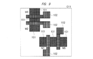
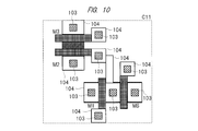
  • 9 to 11 are plan views of the cell C11.
  • elements MOSFETMS, MOSFETs M1 to M3 constituting the cell C11 are formed on the semiconductor substrate 208.
  • 9 to 11 show planes (layouts) in a manufacturing process for forming these elements using semiconductor technology. Since the cross-sectional view shown in FIG. 8 corresponds to the plan view of each manufacturing process shown in FIGS. 9 to 11, the manufacturing process of FIGS. 9 to 11 will be described below with reference to FIG. To do.
  • reference numeral 102 denotes MOSFETMS, M1 to M3 gate electrodes formed on a P-type semiconductor substrate 208 via an insulating film.
  • Reference numeral 101 denotes an N-type semiconductor region formed in the semiconductor substrate 208, which constitutes a source region and a drain region of these MOSFETs.
  • corresponding symbols MS and M1 to M3 are described in regions corresponding to MOSFETMS and M1 to M3, respectively.
  • the N-type semiconductor region 101 constituting the source region and the drain region is formed by self-alignment using the gate electrode as a mask.
  • the N-type semiconductor region 101 is formed by implanting ions into the P-type semiconductor substrate 208 using the gate electrode as a mask. At this time, since the gate electrode is also exposed to ions, charge accumulation may occur.
  • an interlayer insulating film is formed on the semiconductor substrate 208.
  • a contact opening (hole) is formed in the formed interlayer insulating film, and a metal wiring layer 104 is formed on the interlayer insulating film.
  • the metal wiring layer 104 is etched into a shape that forms an electrode of the element.
  • a metal layer 103 is embedded in an opening formed in the interlayer insulating film, and the embedded metal layer 103 causes the metal layer 104 which is an electrode of the element and the gate electrode of the element, and the electrode of the element Are connected between the metal wiring layer 104 and the source and drain regions.
  • FIG. 10 shows a state in which the electrode metal wiring 104 formed by etching in this manner is connected to the element.
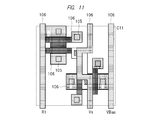
  • FIG. 11 shows the planar shape formed in this way.
  • R1 is a readout line
  • Vs is a ground voltage wiring that supplies a circuit ground voltage
  • VBias is a voltage wiring that supplies a bias voltage VBias.
  • the metal wiring layer 106 forms the readout line R1, the ground voltage wiring Vs, and the voltage wiring VBias.
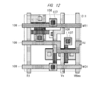
  • FIG. 12 shows a state in which after the metal wiring 106 is formed, an interlayer insulating film is formed, an opening is formed at a predetermined position of the interlayer insulating film, and a metal wiring layer 108 is further formed.
  • the metal wiring layer 108 is etched so as to have a predetermined planar shape so as to constitute a circuit.
  • the metal wiring layer 108 having a predetermined planar shape is electrically connected to the metal wiring layer 106 by a metal wiring layer 107 embedded in the opening.
  • WR1 and WC1 are signal wirings constituting the read signal lines WR1 and WC1 described above, and Vd is a power supply wiring for supplying the power supply voltage Vd.
  • the signal wirings WR1 and WC1 and the power supply wiring Vd are formed by the metal wiring layer 108 that is higher than the metal wiring layer 106.
  • the signal wiring R1 forming the readout line R1 and the signal wirings WR1 and WC1 are arranged (layed out) so as to be orthogonal to each other.
  • the floating gate of MOSFETMS is composed of a plurality of stacked metal layers 102, 104, and 108 and metal layers 103, 105, and 107 that electrically connect the metal layers to them.
  • an ion sensitive film 100 is provided on the metal layer 108 constituting the floating gate.
  • the ion sensitive film 100 is provided on the bottom surface of the well 700 and is surrounded by the well 700.
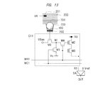
  • FIG. 13 is a circuit diagram showing a configuration of the semiconductor sensor according to the third embodiment.
  • the semiconductor sensor shown in FIG. 13 is similar to the semiconductor sensor shown in FIG. Here, a different part from the semiconductor sensor shown in FIG. 7 is mainly demonstrated.
  • the semiconductor sensor shown in FIG. 13 differs in the circuit configuration of the cell C11. That is, an N-channel MOSFET M4 is added to the cell C11 shown in FIG. 13 with respect to the cell C11 shown in FIG.
  • the MOSFET M4 has a gate connected to the read signal line WR1, similarly to the gate of the MOSFET M3.
  • One electrode of MOSFET M4 is connected to the gate of MOSFET M2, and the other electrode is connected to node N1.
  • the pair of electrodes of the MOSFET M4 is electrically connected (ON) / not connected (OFF) according to the value of the read signal line WR1.
  • the MOSFET M4 that is turned on / off according to the read signal line WR1 is connected in series between the node N1 and the gate of the MOSFET M3.
  • the MOSFET M1 When the threshold voltage of the MOSFET MS is changed, as described above, the MOSFET M1 is turned on by the voltage of the offset cancel signal line WC1. On the other hand, at this time, MOSFET M3 is turned off by read signal line WR1. In this embodiment, when the threshold voltage of the MOSFET MS is changed, the MOSFET M4 is also turned off by the read signal line WR1. As a result, it is possible to prevent a high voltage (bias voltage VBias) used when changing the threshold voltage of MOSFETMS from being applied to the gate of MOSFET M2, thereby improving the reliability of the cell. Become.
  • FIG. 13 shows only one cell C11 as a representative, but in the semiconductor sensor, the cells shown in FIG. 13 are arranged in an array as described in FIG. (Embodiment 4)
  • FIG. 14 is a circuit diagram showing a circuit of the semiconductor sensor according to the fourth embodiment.
  • the semiconductor sensor shown in FIG. 14 is similar to the semiconductor sensor shown in FIG. In FIG. 14, the differences from FIG. 5 are mainly described.
  • the configuration of the cell is different from that of FIG. That is, a plurality of cells arranged in an array are different in FIGS.
  • Each of the cells C11, C12, C21, and C22 shown in FIG. 14 has the same configuration. Therefore, here, the cell C11 will be described as a representative.
  • one electrode of the MOSFET M2 is connected to the corresponding readout line, and the other electrode is connected to one electrode of the MOSFET M3.
  • the other electrode of the MOSFET M3 is connected to the circuit ground voltage Vs.
  • the gate of the MOSFET M2 is connected to the read signal line WR1, and the gate of the MOSFET M3 is connected to one electrode of each of the MOSFET MS and the MOSFET M1.
  • the other electrode of the MOSFET M1 is connected to the circuit ground voltage Vs
  • the other electrode of the MOSFET MS is connected to one electrode of the MOSFET M4, and the other electrode of the MOSFET M4 is connected to the bias voltage VBias.
  • the gate of the MOSFET M4 is connected to the read signal line WR1, and the gate of the MOSFET M1 is connected to the offset cancel signal line WC1.
  • MOSFETMS the role of amplifying the signal of ISFET
  • MOSFET M3 the role of amplifying the signal of ISFET (MOSFETMS) is given to MOSFET M3, not MOSFET M2 (examples in FIGS. 1 and 13).
  • the type of MOSFET can be a P-channel type MOSFET, or the voltage condition applied to the MOSFET can be changed even if it is an N-channel type MOSFET as in the example described so far (bias state change). There are cases where sensitivity can be achieved.
  • the MOSFET M4 between the bias voltage VBias and the MOSFET MS, when changing the threshold voltage of the MOSFET MS, for example, in the array structure of FIG. Although a voltage is applied, this can be avoided. That is, by setting the read signal line WR corresponding to the cell whose threshold voltage is to be changed to a high level and the remaining read signal lines WR to a low level, the bias voltage VBias is applied to the ISFET in the desired cell. You can make it. At this time, since it is possible to prevent a bias voltage from being applied to the ISFET in a cell other than the desired cell, the threshold voltage changes in the unwanted ISFET depending on the voltage applied to other than the desired ISFET. Can be reduced.
  • the read signal line (for example, WR1) corresponding to the cell (for example, C11) including the MOSFET MS is set to the high level, and the remaining read signal line WR2 is changed.
  • the offset cancel signal line WC1 is set to the high level
  • the offset cancel signal line WC2 is set to the low level.
  • the offset cancel signal lines WC1 and WC2 are set to the low level, the read signal line WR (for example, WR1) corresponding to the read cell is set to the high level, and the remaining read signal lines WR2 are set to the low level. To do.
  • MOSFET having the function as described in this embodiment may be performed alone or in combination.
  • a MOSFET M4 may be provided between the bias voltage VBias and the MOSFET MS.
  • the roles of the MOSFETs M2 and M3 may be changed.
  • the N-channel MOSFET may be replaced with a P-channel MOSFET or mixed. (Embodiment 5)
  • FIG. 15 is a schematic cross-sectional view showing the configuration of the semiconductor sensor according to the fifth embodiment.
  • This embodiment is similar to the embodiment shown in FIG. Differences from the embodiment shown in FIG. 7 will be mainly described.
  • a heater 1500 for changing the temperature of each well arranged in an array is provided.
  • the heater 1500 is composed of metal wiring provided between wells close to each other.
  • the metal wiring By supplying a current to the metal wiring arranged between the wells close to each other, the metal wiring generates heat, and the temperature of the well can be changed.
  • a cell including ISFETs arranged in a highly sensitive array a base sequence with higher accuracy can be obtained.
  • FIG. 16 is a block diagram showing a configuration of a biomolecule measuring apparatus when a semiconductor sensor having the heater 1500 shown in FIG. 15 is used. Since the biomolecule measuring apparatus shown in FIG. 16 is similar to the biomolecule measuring apparatus shown in FIG. 6, differences will be mainly described. Compared with the biomolecule measuring apparatus of FIG. 6, the temperature sensor 307 and the heater control circuit 308 (heater in the figure) for controlling the heater 1500 are provided in the ISFET array chip (semiconductor sensor) 1002. The heater control circuit 308 controls the current supplied to the heater 1500 arranged between the wells based on the temperature information from the temperature sensor 307. The temperature sensor 307 makes it possible to accurately capture the temperature at which the actual reaction occurs, and enables detailed temperature control. The temperature sensor 307 may be configured using a semiconductor structure.
  • FIGS. 17A and 17B are waveform diagrams for explaining the operation of the biomolecule measuring apparatus shown in FIG.
  • the horizontal axis indicates time
  • the vertical axis indicates temperature change 1700, reagent supply state 1701, signals 1702 and 1704 from ISFET from the top in FIG. Respectively.
  • FIG. 17A shows a case where hot electrons are not injected into the ISFET MOSFET MS
  • FIG. 17B shows the case of the ISFET MOSFET MS. The case where such hot electron injection is performed is shown.
  • Washing is performed to wash away the reagents used in the previous cycle reaction.
  • the cleaning liquid used in this cleaning for example, a cleaning liquid having a low temperature of 5 ° C. is used. Thereafter, a reaction reagent kept at a low temperature is introduced. In this state, since the temperature is low, for example, the DNA elongation reaction itself does not occur, or even if it occurs, there is a very small probability.
  • the reaction reagent itself has a pH concentration.
  • the ISFET outputs a constant signal 1703 (dashed line).
  • this signal is referred to as a reaction reagent-derived signal (BG).
  • a current is supplied to the heater 1500, the temperature in each well 700 is raised, and the temperature of the reagent is raised. Then, a DNA elongation reaction is caused by the reaction reagent, and the ISFET detects a change in the hydrogen ion concentration changed by the reaction reagent, and outputs a signal corresponding to the elongation reaction. That is, a difference between the constant signal 1703 and the signal 1702 becomes an extension signal corresponding to the extension reaction. If the ISFET has an amplification function and has no offset, the pH concentration of the reaction reagent at this low temperature can be detected with high sensitivity by the extension reaction after the temperature is raised. Thereafter, the current to the heater is stopped, and the reaction reagent is flowed by flowing a low temperature washing solution, the temperature is lowered, and the preparation for the next measurement is ready. Repeat this.
  • the pH concentration of the reaction reagent at a low temperature is detected as a reaction reagent-derived signal (BG). For this reason, it is necessary to remove this by subsequent processing (such as calculation processing of the data processing device 311 (FIG. 16)).
  • BG reaction reagent-derived signal
  • the signal from the reaction reagent at a low temperature is larger than the change in the extension reaction. When aiming at high sensitivity, this also appears as a large background (BG) and is often in the way. However, this can be reduced by using an operation that reduces the offset of the ISFET.
  • the reaction of biomolecules is on the order of seconds, while the hot electron injection operation is on the order of several tens of microseconds. Therefore, even if hot electron injection is performed during the measurement, the overall measurement is not delayed. In addition, once set, it may not be necessary to change the threshold voltage for each measurement.
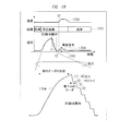
  • FIG. 18 is a waveform diagram showing in detail the hot electron injection operation performed in FIG.
  • the waveform shown in FIG. 17B is shown again on the upper side.
  • the lower part of FIG. 18 shows a waveform obtained by enlarging the signal 1704 from the ISFET, particularly from time t1 to time t2.
  • the signal 1704 shown in the lower side of FIG. 18 changes depending on the verify operation.
  • a signal from the reaction reagent at a low temperature is output (time t1), as described in FIG. 3, the injection of hot electrons (HC) and the verify operation of the ISFET are repeated with respect to the floating gate of the ISFET (MOSFETMS).
  • hot electron injection (1) is performed, and whether or not the output of the cell (ISFET) is within a predetermined range (verify operation (2)) is performed, and is not within the predetermined range
  • verify operation (2) is repeated.
  • hot electrons are not injected.
  • the reaction with the reaction reagent at a low temperature is a reaction of the order of seconds.
  • the hot electron (HC) injection + verify operation is on the order of several tens of microseconds. Therefore, even if hot electron injection and verify operation are repeated 100 times, it is on the order of several milliseconds. That is, in the figure, for the sake of explanation, the hot electron (HC) injection + verify operation is enlarged and written, but in an actual operation, this operation hardly affects the entire measurement. In this embodiment, it can be considered that hot electron injection and a verify operation are repeated so that the voltage of the signal 1704 falls within a predetermined range instead of the threshold voltage of the ISFET. . (Embodiment 6)
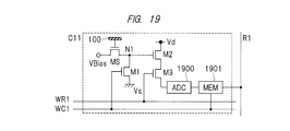
  • FIG. 19 is a circuit diagram showing a configuration of a cell according to the sixth embodiment. Since the configuration of the cell shown in FIG. 19 is similar to the configuration of the cell shown in FIG. 1, differences will be mainly described.
  • the cell C11 shown in FIG. 19 includes an analog / digital conversion circuit ADC1900 that converts an analog value, which is an output signal of the ISFET, into a digital bit, and a memory circuit MEM1901 that temporarily stores the analog / digital conversion circuit.
  • ADC1900 analog / digital conversion circuit
  • MEM1901 memory circuit
  • each cell has a function of reducing the offset of the ISFET and a function of amplifying the signal of the ISFET, another factor that hinders high sensitivity is when signals are sent from these cells to the subsequent stage.
  • the output of the ISFET is directly converted into a digital signal and held for each cell. This makes it possible to maximize the performance of the cell with high sensitivity and reduced offset.
  • FIG. 20 is a circuit diagram showing a modification of FIG.
  • a common analog / digital conversion circuit ADC200 and memory circuit MEM201 are provided for a plurality of cells C11 and C21.
  • the cell C11 and the cell C21 are operated in a time division manner.
  • the analog / digital conversion circuit ADC 200 and the memory circuit MEM 201 can be shared by a plurality of cells, and the area can be reduced.
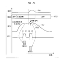
  • FIG. 21 is a waveform diagram showing an operation when the cell according to the sixth embodiment is used. That is, it is a waveform diagram showing the operation of the biomolecule measuring apparatus provided with the analog / digital conversion circuit ADC for each cell or for each of a plurality of cells.
  • This figure is similar to FIG. That is, as described in FIG. 17A, the reaction reagent-derived signal (BG), which is a reaction of the reaction reagent itself at a low temperature, is digitized and taken into the memory circuit MEM between time t0 and time t1. (Data MEM0). Next, the temperature is raised and a signal in an actual reaction is captured between time t2 and time t3 (data MEM1).
  • BG reaction reagent-derived signal
  • FIG. 22 is a circuit diagram showing a configuration of the semiconductor sensor according to the seventh embodiment.
  • This embodiment is an example in which higher sensitivity is pursued.
  • each cell including the ISFET can be highly sensitive. Since a highly sensitive cell can be obtained, it is desirable that the reference used for determining the cell output is also highly accurate. In this embodiment, a highly accurate reference is realized by using two types of cells having well sizes.
  • each of the cells C11 and C12 has the same circuit configuration as the cell C11 shown in FIG.
  • the dimensions of the well provided with the ion sensitive film 100 connected to the ISFETs of the cells C11 and C12 are different between the cell C11 and the cell C12. That is, the well 700 to which the cell C11 is bound is dimensioned so that the bead 701 to which the measurement molecule is attached is attached, and the well 700 to which the cell C12 is bound is dimensioned so that the bead 701 is not attached thereto.
  • the well size or shape is changed to form a well in which beads are not attached.
  • the read lines RCR and RCL of the cells C11 and C12 thus arranged are arranged along the pair of inputs of the sense amplifier SA.
  • a pair of inputs of the sense amplifier SA is always a pair of beads 700 attached and those not attached (a state where no beads are originally contained in a well that can be attached). Yes, but this does not contribute to the measurement).
  • a reference of the sense amplifier SA it is possible to always obtain a well signal that has a reaction reagent but does not react with a biological substance.
  • FIG. 22 shows an example in which the size of the well opening coupled to the cell C12 is larger than that of the well coupled to the cell C11.
  • the opening may be smaller than the diameter of the bead 700. In this way, it is possible to prevent the beads from being attached to the well.
  • the beads enter the well coupled to the cell C12. However, the entering beads are washed out in the washing step.
  • reference numeral 1500 denotes a heater.
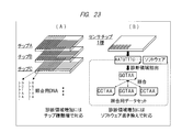
  • the high-sensitivity cell having the ISFET is realized by the plurality of embodiments described so far. Taking a DNA sequencer in a high-sensitivity biomolecule measuring apparatus using this as an example, embodiments of a data processing apparatus are shown in FIGS. 23A and 23B and FIG.
  • a chip (chip A to chip C) that reacts with a specific DNA base called a DNA chip is prepared to increase sensitivity at a low cost. Is realized. However, when the necessary diagnostic items are changed, the measurement content and range change, and the chip needs to be remade.
  • an array can be realized using a plurality of cells each having an ISFET, reducing the offset of the ISFET, and having an amplifying function.
  • a highly sensitive ISFET array can be realized.
  • a semiconductor sensor having such an array is general-purpose and can read any base sequence. Therefore, as shown in FIG. 23B, the main focus is not reading itself, but how important information necessary for subsequent necessary diagnostic items can be easily obtained by the data processing device portion.
  • measurement is performed with a semiconductor sensor having a high-sensitivity ISFET described in a plurality of embodiments, and the data processor unit It corresponds by software.
  • the configurations described in the plurality of embodiments can reduce the development of a plurality of chips in such a DNA sequencer and can also reduce the cost.
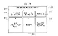
  • FIG. 24 is a block diagram showing a block configuration of a data processing apparatus combined with an ISFET array described in a plurality of embodiments. Since the method for examining the DNA information read for each diagnosis is different, in order to perform this at high speed, the data processing apparatus is configured by a dynamic reconfigurable high-speed matching board 2400 whose function can be dynamically changed.
  • the sequencer output is stored in the sequencer output data buffer 2401. This is compared with the reference 2406 updated with information from the cloud every day by the high-speed pattern patching engine 2404.
  • the high-speed pattern patching engine 2404 includes a base sequence useful for detection that is also updated in the cloud as a reference table, and performs pattern matching at high speed based on the same principle as that of the CAM.
  • the entire board is managed by the control CPU 2405, and authentication, data trace information 2403, and the data's authenticity are checked.
  • the IO unit 2403 has an encryption function. In this way, by combining the board with the inexpensive and highly sensitive ISFET array described in the embodiment, a device for obtaining valuable information from measured data at high speed and at low cost based on individual needs or the latest medical data. realizable.

Landscapes

  • Health & Medical Sciences (AREA)
  • Life Sciences & Earth Sciences (AREA)
  • Chemical & Material Sciences (AREA)
  • Molecular Biology (AREA)
  • Physics & Mathematics (AREA)
  • Chemical Kinetics & Catalysis (AREA)
  • Microelectronics & Electronic Packaging (AREA)
  • Engineering & Computer Science (AREA)
  • Spectroscopy & Molecular Physics (AREA)
  • Electrochemistry (AREA)
  • Analytical Chemistry (AREA)
  • Biochemistry (AREA)
  • General Health & Medical Sciences (AREA)
  • General Physics & Mathematics (AREA)
  • Immunology (AREA)
  • Pathology (AREA)
  • Investigating Or Analyzing Materials By The Use Of Electric Means (AREA)
  • Apparatus Associated With Microorganisms And Enzymes (AREA)

Abstract

A biomolecule measuring device, wherein a semiconductor sensor for detecting ions generated by a reaction between a biomolecule sample and a reagent is installed. The semiconductor sensor comprises a plurality of cells which are disposed on a semiconductor substrate and detect ions, and a plurality of sense lines. Each of the plurality of cells includes an ISFET which has a floating gate and detects ions, a first MOSFET (M2) which amplifies the output of the ISFET, and a second MOSFET (M3) which selectively transmits the output of the first MOSFET to a sense line (R1) corresponding thereto. Each of the plurality of cells is provided with a third MOSFET (M1) which generates hot electrons in the ISFET and injects an electric charge into the floating gate of the ISFET. The second MOSFET and the third MOSFET are separately controlled.

Description

生体分子計測装置Biomolecule measuring device
 本発明は、生体分子計測装置に関し、特に半導体技術を用いた生体分子計測装置に関する。 The present invention relates to a biomolecule measuring apparatus, and more particularly to a biomolecule measuring apparatus using semiconductor technology.
 近年、半導体技術を用いた生体分子計測装置が注目されている。特許文献1には、半導体技術で製造したpHセンサアレイ(半導体センサ)によって、デオキシリボ核酸(DNA)の塩基配列を低コスト、高速に決定するDNAシーケンサが記載されている。半導体センサは、対象とする生体分子試料と試薬との反応を電気信号の強弱で定量化することができる。そのため、従来のような高価な蛍光試薬が不要で、コスト面で有利である。また、半導体の微細加工技術によって数百万から数億のセンサを、1個の半導体基板に集積可能で、並列に測定できるため、測定のスループットも向上しやすい。 In recent years, biomolecule measuring devices using semiconductor technology have attracted attention. Patent Document 1 describes a DNA sequencer that determines the base sequence of deoxyribonucleic acid (DNA) at low cost and at high speed using a pH sensor array (semiconductor sensor) manufactured by semiconductor technology. The semiconductor sensor can quantify the reaction between the target biomolecule sample and the reagent based on the strength of the electric signal. Therefore, an expensive fluorescent reagent as in the prior art is unnecessary, which is advantageous in terms of cost. Also, millions to hundreds of millions of sensors can be integrated on a single semiconductor substrate by a semiconductor microfabrication technique, and measurement can be performed in parallel, so that measurement throughput is easily improved.
 生体分子計測装置の分野で特に良く用いられる半導体センサの一つは、イオン感応性電界効果トランジスタ(Ion Sensitive Field Effect Transistor:以下、ISFETと称する)である。ISFETとは、イオン感応膜上に誘起される界面電位を測定するデバイスである。 One of the semiconductor sensors that are particularly often used in the field of biomolecule measuring devices is an ion-sensitive field effect transistor (hereinafter referred to as ISFET). An ISFET is a device that measures the interfacial potential induced on an ion sensitive membrane.
 特許文献1では、ISFETを用いることによって、試薬によるDNAの伸長反応によって発生する水素イオン濃度の変化を測定している。DNAを構成する塩基には4種類があるが、その特定の塩基でのみ反応し水素イオンを発生する試薬を用いることで、水素イオン濃度変化から塩基の種類を特定することが可能となる。ここで、4種類の塩基とは、アデニン、チミン、シトシン、グアニンである。 In Patent Document 1, a change in hydrogen ion concentration generated by a DNA elongation reaction by a reagent is measured by using an ISFET. There are four types of bases that make up DNA. By using a reagent that reacts only with a specific base to generate hydrogen ions, the type of base can be specified from changes in the hydrogen ion concentration. Here, the four types of bases are adenine, thymine, cytosine, and guanine.
 水素イオン濃度の変化による理論上の電圧変化は、理論的にはネルンストの式と呼ばれる式から求めることができる。例えば、25℃において、電圧変化は、おおよそ59mV/pHである。この変化(変動)が、ISFETのゲート電圧に変化を与え、ISFETの出力電流が変化する。実際には、水素イオン濃度の変動に対する電圧変動は、理論値より低く、pHあたり数10mV程度となる。上記DNAの伸長反応によって発生する水素イオン濃度の変化は、反応を起させるDNA鎖の数と反応を起させる空間の大きさや試薬にもよるが、pHの変化では0.1mV程度である。そのため、ISFETの出力信号の変化は極めて小さい。 The theoretical voltage change due to the change in hydrogen ion concentration can theoretically be obtained from an equation called the Nernst equation. For example, at 25 ° C., the voltage change is approximately 59 mV / pH. This change (fluctuation) changes the gate voltage of the ISFET, and the output current of the ISFET changes. Actually, the voltage fluctuation with respect to the fluctuation of the hydrogen ion concentration is lower than the theoretical value, and is about several tens mV per pH. The change in the hydrogen ion concentration generated by the DNA elongation reaction depends on the number of DNA strands causing the reaction, the size of the space causing the reaction, and the reagent, but it is about 0.1 mV when the pH changes. For this reason, the change in the output signal of the ISFET is extremely small.
 これを解決するために、ISFETの高感度化が検討されている。この例として特許文献2に記載されている技術がある。特許文献2においては、多数のISFETが、アレイ状に配置されており、その図75Fには、水素イオンの濃度変化を検出する単位セルが、75F1として示されている。この単位セル75F1は、高感度化の機能を備えている。図75Fにおいて、ISFETとして示されている部分が、ISFETの回路表現であり、ISFETは、イオン感応膜(部分)75F6と、これがゲートに接続されたとMOSFET(トランジスタ)75F2とから構成されている。同図において、75F3はバイアス電流を与えるMOSFETであり、75F4は出力信号線75F7(Column Bus)と接続するためのMOSFETである。また、同図において、Row Selectは、単位セル75F1を選択する信号線である。 In order to solve this, high sensitivity of ISFET is being studied. As an example, there is a technique described in Patent Document 2. In Patent Document 2, a large number of ISFETs are arranged in an array, and in FIG. 75F, a unit cell for detecting a change in the concentration of hydrogen ions is shown as 75F1. The unit cell 75F1 has a function of increasing sensitivity. In FIG. 75F, the portion shown as ISFET is a circuit representation of ISFET, and the ISFET is composed of an ion sensitive film (portion) 75F6 and a MOSFET (transistor) 75F2 connected to the gate. In the figure, 75F3 is a MOSFET for applying a bias current, and 75F4 is a MOSFET for connecting to an output signal line 75F7 (Column Bus). In the figure, Row Select is a signal line for selecting the unit cell 75F1.
 この特許文献2においては、ISFETの高感度化はMOSFET75F5によってなされる。すなわち、MOSFET75F2の出力はMOSFET75F5のゲートに入力されている。水素イオン濃度の変化によって、MOSFET75F2とイオン感応膜75F6で構成されたところのISFETのゲート電圧が変化する。この変化により、ISFETの出力電流が変化する。この変化は、MOSFET75F5で一旦増幅される。すなわち、水素イオン濃度の変化によるISFET出力電流の小さな変化は増幅される。増幅された後、MOSFET75F4を介して出力信号線75F7に出力される。これにより、ISFETの高感度化を図る様にしている。 In this Patent Document 2, the sensitivity of the ISFET is increased by the MOSFET 75F5. That is, the output of the MOSFET 75F2 is input to the gate of the MOSFET 75F5. The gate voltage of the ISFET formed by the MOSFET 75F2 and the ion sensitive film 75F6 is changed by the change of the hydrogen ion concentration. Due to this change, the output current of the ISFET changes. This change is once amplified by the MOSFET 75F5. That is, a small change in ISFET output current due to a change in hydrogen ion concentration is amplified. After being amplified, it is output to the output signal line 75F7 via the MOSFET 75F4. As a result, the sensitivity of the ISFET is increased.
 一方、ISFETのデバイス中に、測定対象のイオンに由来する以外の電荷が存在すると、これは測定誤差の要因となる。一般に、半導体プロセスでは、デバイスの製造時にプラズマによる加工やイオン注入を行うため、デバイス中に電荷が蓄積されやすいという課題がある。係る課題に関連して、非特許文献1には、特に、イオン感応膜、保護膜、電極の界面や、フローティング電極、ゲート酸化膜に電荷が蓄積されることが記載されている。非特許文献1には、こうした電荷の蓄積により、ISFETのしきい値電圧が±10V程度オフセットすることが記載されている。 On the other hand, if charges other than those derived from ions to be measured are present in the ISFET device, this causes measurement errors. Generally, in semiconductor processes, there is a problem that charges are easily accumulated in a device because processing or ion implantation is performed by plasma at the time of manufacturing the device. In relation to this problem, Non-Patent Document 1 describes that charges are accumulated particularly in an ion sensitive film, a protective film, an electrode interface, a floating electrode, and a gate oxide film. Non-Patent Document 1 describes that the threshold voltage of the ISFET is offset by about ± 10 V due to such charge accumulation.
 この様なオフセットが存在すると、特許文献2の図75Fに示されている様な構成では、オフセットもそのまま増幅されてしまうことになる。 If such an offset exists, in the configuration as shown in FIG. 75F of Patent Document 2, the offset is also amplified as it is.
 この様なオフセットを取り除く従来技術として、紫外線を照射することで電荷にエネルギーを与えてデバイス外部へと抜き出す方法が、特許文献1に記載されている。また、紫外線の照射は、例えば10時間など、長時間行う必要があることが、非特許文献2に記載されている。また別の方法として、ホットエレクトロン注入により、捕獲電荷によるしきい値電圧の変化を低減できる旨が、非特許文献3に記載されている。 As a conventional technique for removing such an offset, Patent Document 1 discloses a method of applying energy to a charge by irradiating ultraviolet rays and extracting the charge to the outside of the device. Further, it is described in Non-Patent Document 2 that irradiation with ultraviolet rays needs to be performed for a long time, for example, 10 hours. As another method, Non-Patent Document 3 describes that a change in threshold voltage due to trapped charges can be reduced by hot electron injection.
特表2010-513869号公報Special table 2010-513869 gazette 米国特許出願公開第2010/0301398A1号公報US Patent Application Publication No. 2010 / 0301398A1
 ISFETの高感度化を図るために、増幅作用のあるMOSFETを挿入すると、ISFETの大きなオフセットも増幅してしまう。このため、本来の水素イオン濃度の変化(PHの変化)を検出することが困難となってしまう。また、紫外線を照射することにより、電荷を放出する技術においては、紫外線を長時間照射することが必要であり、試料である生体分子を破壊する恐れもある。非特許文献3では、オフセットを低減する方法に関し、単体ISFETへのホットエレクトロン注入については検討されている。しかしながら、特に複数のISFETをアレイ状に配置した生体分子測定装置に好適な方法については何ら検討がなされていない。 If a MOSFET having an amplifying action is inserted to increase the sensitivity of the ISFET, a large offset of the ISFET is also amplified. For this reason, it becomes difficult to detect a change in the original hydrogen ion concentration (change in PH). Further, in the technology for releasing electric charges by irradiating ultraviolet rays, it is necessary to irradiate ultraviolet rays for a long time, and there is a possibility of destroying a biomolecule as a sample. Non-Patent Document 3 discusses hot electron injection into a single ISFET with respect to a method for reducing offset. However, no investigation has been made on a method particularly suitable for a biomolecule measuring apparatus in which a plurality of ISFETs are arranged in an array.
 本発明の目的は、複数のISFETを有し、高感度な生体分子計測装置を提供することである。 An object of the present invention is to provide a highly sensitive biomolecule measuring device having a plurality of ISFETs.
 本発明の前記ならびにそのほかの目的と新規な特徴は、本明細書の記述および添付図面から明らかになるであろう。 The above and other objects and novel features of the present invention will be apparent from the description of this specification and the accompanying drawings.
 本願において開示される発明のうち、代表的なものの概要を簡単に説明すれば、次のとおりである。 Of the inventions disclosed in this application, the outline of typical ones will be briefly described as follows.
 すなわち、生体分子計測装置には、生体分子試料と試薬との反応により発生するイオンを検知する半導体センサが設置される。当該半導体センサは、半導体基板において、アレイ状に配置され、それぞれがイオンを検知する複数のセルと、アレイに配置された複数の読み出し線とを有している。アレイ状に配置された複数のセルのそれぞれは、フローティングゲートを有し、イオンの濃度の変化を検知するISFETと、ISFETの出力を受けるゲートを有し、ISFETの出力を増幅する第1のMOSFETと、第1のMOSFETの出力を、複数の読み出し線の内の対応する読み出し線に、選択的に伝達する第2のMOSFETとを含んでいる。さらに、複数のセルのそれぞれは、ISFETに接続され、ISFETにおいてホットエレクトロン(ホットキャリア)を発生させ、電荷をISFETのフローティングゲートに注入させる第3のMOSFETを具備している。ここで、第2のMOSFETと第3のMOSFETとは、別々に制御されることができる。 That is, the biomolecule measuring apparatus is provided with a semiconductor sensor that detects ions generated by the reaction between the biomolecule sample and the reagent. The semiconductor sensor is arranged in an array on a semiconductor substrate, and has a plurality of cells each detecting ions and a plurality of readout lines arranged in the array. Each of the plurality of cells arranged in an array has a floating gate, an ISFET that detects a change in the concentration of ions, a gate that receives the output of the ISFET, and a first MOSFET that amplifies the output of the ISFET And a second MOSFET for selectively transmitting the output of the first MOSFET to a corresponding readout line of the plurality of readout lines. Further, each of the plurality of cells includes a third MOSFET that is connected to the ISFET, generates hot electrons (hot carriers) in the ISFET, and injects charges into the floating gate of the ISFET. Here, the second MOSFET and the third MOSFET can be controlled separately.
 第2のMOSFETを制御することにより、第1のMOSFETにより増幅されたISFETの出力を読み出すことができる。例えば、読み出した出力に基づいて、第3のMOSFETを制御する。第3のMOSFETを制御することによって、ISFETにおいてホットエレクトロン(ホットキャリア)が発生され、発生した電荷をISFETのフローティングゲートに注入させることができる。これにより、読み出した出力に基づいて、ISFETのしきい値電圧を設定することが可能となる。この様にして、アレイ状に配置された複数のセルのそれぞれにおけるISFETのしきい値電圧を設定することにより、製造時等において蓄積された電荷によって生じたしきい値電圧の変動を、複数のISFET間で低減することが可能となり、高感度な生体分子計測装置を得ることが可能となる。 By controlling the second MOSFET, the output of the ISFET amplified by the first MOSFET can be read. For example, the third MOSFET is controlled based on the read output. By controlling the third MOSFET, hot electrons (hot carriers) are generated in the ISFET, and the generated charges can be injected into the floating gate of the ISFET. Thereby, the threshold voltage of the ISFET can be set based on the read output. In this way, by setting the threshold voltage of the ISFET in each of a plurality of cells arranged in an array, fluctuations in the threshold voltage caused by charges accumulated during manufacturing or the like can be reduced. It becomes possible to reduce between ISFETs, and a highly sensitive biomolecule measuring device can be obtained.
 一実施の形態においては、生体分子計測装置は、複数のセルのそれぞれにおけるISFETのフローティングゲートから、半導体基板へトンネル電流を流させる第1動作モードを有する。第1動作モードを実行することにより、複数のISFETのそれぞれのしきい値電圧は、所定の方向(高い方向あるいは低い方向)へ変化する。これにより、複数のISFETのしきい値電圧を揃えることが可能となる。 In one embodiment, the biomolecule measuring device has a first operation mode in which a tunnel current flows from the floating gate of the ISFET in each of the plurality of cells to the semiconductor substrate. By executing the first operation mode, the threshold voltage of each of the plurality of ISFETs changes in a predetermined direction (high direction or low direction). As a result, the threshold voltages of a plurality of ISFETs can be made uniform.
 また、一実施の形態においては、生体分子計測装置は、第3のMOSFETを制御して、ISFETのフローティングゲートへ電荷を注入する動作と、第2のMOSFETを制御して、ISFETの出力を、読み出し線へ伝達し、ISFETのしきい値電圧が所定の範囲にあるか否かを判定する動作とを交互に行わせ、複数のセルのそれぞれにおけるISFETのしきい値電圧が、所定の範囲に納まる様にする。 In one embodiment, the biomolecule measuring device controls the third MOSFET to inject charges into the floating gate of the ISFET, and controls the second MOSFET to output the ISFET. The operation is alternately performed to determine whether or not the threshold voltage of the ISFET is within a predetermined range, and the threshold voltage of the ISFET in each of the plurality of cells is within the predetermined range. Make it fit.
 さらに、一実施の形態においては、ISFETのフローティングゲートへ電荷を注入する動作の前に、前記した第1動作モードが実行される。これにより、複数のISFETのそれぞれのしきい値電圧を、所定の方向へ変化させた後、それぞれのISFETのしきい値電圧が所定の範囲に納まる様に制御されるため、より正確に、各ISFETのしきい値電圧を所定の範囲に納めることが可能となる。 Furthermore, in one embodiment, the first operation mode described above is executed before the operation of injecting charges into the floating gate of the ISFET. Thus, after changing the threshold voltage of each of the plurality of ISFETs in a predetermined direction, the threshold voltages of the respective ISFETs are controlled so as to be within a predetermined range. It becomes possible to keep the threshold voltage of the ISFET within a predetermined range.
 本願において開示される発明のうち、代表的なものによって得られる効果を簡単に説明すれば、以下のとおりである。
 高感度な生体分子計測装置を提供することができる。
Of the inventions disclosed in the present application, effects obtained by typical ones will be briefly described as follows.
A highly sensitive biomolecule measuring apparatus can be provided.
実施の形態1に係わるセルの構成を示す回路図である。FIG. 3 is a circuit diagram showing a configuration of a cell according to the first embodiment. (A)および(B)は、オフセットをキャンセルする仕組みを説明するための模式図である。(A) And (B) is a schematic diagram for demonstrating the mechanism which cancels offset. (A)~(G)は、実施の形態1の動作を示す波形図である。(A) to (G) are waveform diagrams showing the operation of the first embodiment. (A)~(E)は、実施の形態1の他の動作を示す波形図である。(A) to (E) are waveform diagrams showing other operations of the first embodiment. 実施の形態2に係わる半導体センサの構成を示す回路図である。FIG. 6 is a circuit diagram illustrating a configuration of a semiconductor sensor according to a second embodiment. 生体分子計測装置の構成を示すブロック図である。It is a block diagram which shows the structure of a biomolecule measuring device. 半導体センサの模式的な断面図である。It is a typical sectional view of a semiconductor sensor. 半導体センサの断面図である。It is sectional drawing of a semiconductor sensor. 半導体センサの平面図である。It is a top view of a semiconductor sensor. 半導体センサの平面図である。It is a top view of a semiconductor sensor. 半導体センサの平面図である。It is a top view of a semiconductor sensor. 半導体センサの平面図である。It is a top view of a semiconductor sensor. 実施の形態3に係わる半導体センサの回路図である。6 is a circuit diagram of a semiconductor sensor according to Embodiment 3. FIG. 実施の形態4に係わる半導体センサの回路を示す回路図である。FIG. 6 is a circuit diagram showing a circuit of a semiconductor sensor according to a fourth embodiment. 実施の形態5に係わる半導体センサの模式的な断面図である。FIG. 9 is a schematic cross-sectional view of a semiconductor sensor according to a fifth embodiment. 生体分子計測装置の構成を示すブロック図である。It is a block diagram which shows the structure of a biomolecule measuring device. (A)および(B)は、生体分子計測装置の動作を説明する波形図である。(A) And (B) is a wave form diagram explaining operation | movement of a biomolecule measuring device. 生体分子計測装置の動作を説明する波形図である。It is a wave form diagram explaining operation | movement of a biomolecule measuring apparatus. 実施の形態6に係わるセルの構成を示す回路図である。FIG. 10 is a circuit diagram illustrating a configuration of a cell according to a sixth embodiment. セルの構成を示す回路図である。It is a circuit diagram which shows the structure of a cell. 生体分子計測装置の動作を説明する波形図である。It is a wave form diagram explaining operation | movement of a biomolecule measuring apparatus. 実施の形態7に係わる半導体センサの構成を示す回路図である。FIG. 10 is a circuit diagram showing a configuration of a semiconductor sensor according to a seventh embodiment. (A)および(B)は、生体分子計測装置のデータ処理部分の機能を示す図である。(A) And (B) is a figure which shows the function of the data processing part of a biomolecule measuring device. 生体分子計測装置のデータ処理部分の構成を示す図である。It is a figure which shows the structure of the data processing part of a biomolecule measuring device.
 以下、本発明の実施の形態を図面に基づいて詳細に説明する。なお、実施の形態を説明するための全図において、同一部分には原則として同一の符号を付し、その繰り返しの説明は、原則として省略する。 Hereinafter, embodiments of the present invention will be described in detail with reference to the drawings. Note that components having the same function are denoted by the same reference symbols throughout the drawings for describing the embodiment, and the repetitive description thereof will be omitted.
 以下の実施の形態においては便宜上その必要があるときは、複数のセクションまたは実施の形態に分割して説明するが、特に明示した場合を除き、それらはお互いに無関係なものではなく、一方は他方の一部または全部の変形例、詳細、補足説明等の関係にある。また、以下の実施の形態において、要素の数等(個数、数値、量、範囲等を含む)に言及する場合、特に明示した場合および原理的に明らかに特定の数に限定される場合等を除き、その特定の数に限定されるものではなく、特定の数以上でも以下でも良い。また、以下の実施の形態において、その構成要素(要素ステップ等も含む)は、特に明示した場合および原理的に明らかに必須であると考えられる場合等を除き、必ずしも必須のものではないことはいうまでもない。 In the following embodiments, when it is necessary for the sake of convenience, the description will be divided into a plurality of sections or embodiments. However, unless otherwise specified, they are not irrelevant to each other. There are some or all of the modifications, details, supplementary explanations, and the like. Further, in the following embodiments, when referring to the number of elements (including the number, numerical value, quantity, range, etc.), especially when clearly indicated and when clearly limited to a specific number in principle, etc. Except, it is not limited to the specific number, and may be more or less than the specific number. Further, in the following embodiments, the constituent elements (including element steps) are not necessarily indispensable unless otherwise specified and clearly considered essential in principle. Needless to say.
 同様に、以下の実施の形態において、構成要素等の形状、位置関係等に言及するときは、特に明示した場合および原理的に明らかにそうでないと考えられる場合等を除き、実質的にその形状等に近似または類似するもの等を含むものとする。このことは、上記数値および範囲についても同様である。
 (実施の形態1)
Similarly, in the following embodiments, when referring to the shapes, positional relationships, etc. of the components, etc., the shapes are substantially the same unless otherwise specified, or otherwise apparent in principle. And the like are included. The same applies to the above numerical values and ranges.
(Embodiment 1)
 半導体センサは、1個の半導体基板に半導体技術で製造される。すなわち、半導体センサは、半導体技術で1個の半導体基板に形成され、半導体基板においてアレイ状に配置された複数のセルを有する。生体分子測定装置には、例えば、後で図6を用いて説明するが、半導体センサが設置される。 Semiconductor sensors are manufactured on a single semiconductor substrate using semiconductor technology. That is, the semiconductor sensor has a plurality of cells formed in one semiconductor substrate by semiconductor technology and arranged in an array on the semiconductor substrate. For example, a semiconductor sensor is installed in the biomolecule measuring apparatus, which will be described later with reference to FIG.
 本実施の形態においては、アレイ状に配置された複数のセルのそれぞれは、セルの高感度化を図るために、ISFETと、増幅作用のあるトランジスタを備え、更に、ISFETのオフセットを低減する動作が可能なトランジスタと、この動作に必要な信号線とを備える。以下、複数の実施の形態を説明するが、以下の説明では、トランジスタとして、半導体基板に形成されたNチャンネル型電界効果トランジスタ(MOSFET)を用いるものとする。勿論、Nチャンネル型MOSFETは、一例であり、種々のトランジスタを用いることが可能である。
 図1は、本実施の形態に係わるセルの構成を示す回路図である。同図には、アレイ状に配置された複数のセルのうちの1個のセルC11の構成が示されている。アレイ状に配置された複数のセルは、互いに同じ構成にされている。
In the present embodiment, each of a plurality of cells arranged in an array includes an ISFET and an amplifying transistor in order to increase the sensitivity of the cell, and further reduces the offset of the ISFET. And a signal line necessary for this operation. Hereinafter, a plurality of embodiments will be described. In the following description, an N-channel field effect transistor (MOSFET) formed on a semiconductor substrate is used as a transistor. Of course, the N-channel MOSFET is an example, and various transistors can be used.
FIG. 1 is a circuit diagram showing a configuration of a cell according to the present embodiment. The figure shows the configuration of one cell C11 among a plurality of cells arranged in an array. The plurality of cells arranged in an array have the same configuration.
 図1において、M1~M3のそれぞれは、MOSFETである。セルC11は、ISFETと、第1のMOSFETM2と、第2のMOSFETM3と、第3のMOSFETM1とを含んでいる。ISFETは、フローティングゲートを有するMOSFETMSとイオン感応膜100とを有している。ISFETのデバイス構造は、後で図2の(A)および(B)を用いて一例を説明するが、ISFETのイオン感応膜100は、溶液に浸される。また、ISFETに設けられているMOSFETMSは、フローティングゲートを有するMOSFETとして動作する。 In FIG. 1, each of M1 to M3 is a MOSFET. The cell C11 includes an ISFET, a first MOSFET M2, a second MOSFET M3, and a third MOSFET M1. The ISFET has a MOSFET MS having a floating gate and an ion sensitive film 100. An example of the device structure of the ISFET will be described later with reference to FIGS. 2A and 2B, and the ion sensitive film 100 of the ISFET is immersed in a solution. Further, the MOSFET MS provided in the ISFET operates as a MOSFET having a floating gate.
 MOSFETMSのドレイン電極(端子)には、動作に応じた電圧がバイアス電圧VBiasとして印加され、MOSFETMSのソース電極(端子)は、ノードN1に接続されている。MOSFETMSのバックゲート(この例では、半導体基板)には、制御電圧VBがバックバイアス電圧として印加される。この制御電圧VBは、セルC11内の他のMOSFETM1~M3のバックゲートに印加されるバックバイアス電圧とは独立にしてもよいし、共通にしてもよい。図1には、MOSFETM1のバックゲートにも制御電圧VBが印加されている例が示されている。なお、独立に印加する場合は、半導体技術では良く知られているように、電気的に他のMOSFETと絶縁するために電気極性の異なる半導体領域を設けて形成する。 A voltage corresponding to the operation is applied as a bias voltage VBias to the drain electrode (terminal) of the MOSFETMS, and the source electrode (terminal) of the MOSFETMS is connected to the node N1. A control voltage VB is applied as a back bias voltage to the back gate (in this example, a semiconductor substrate) of the MOSFET MS. The control voltage VB may be independent from or common to the back bias voltage applied to the back gates of the other MOSFETs M1 to M3 in the cell C11. FIG. 1 shows an example in which the control voltage VB is also applied to the back gate of the MOSFET M1. In the case of independent application, as is well known in the semiconductor technology, semiconductor regions having different electrical polarities are provided in order to be electrically insulated from other MOSFETs.
 MOSFETMSのソース電極が接続されたノードN1は、MOSFETM1とM2とに接続している。この構成に、本実施の形態の一つの特徴がある。すなわち、ISFET内のMOSFETMSのソース電極(ノードN1)は、第3のMOSFETM1のドレイン電極に接続されている。また、第3のMOSFETM1のゲートはオフセットキャンセル信号線WC1に接続され、オフセットキャンセル信号線WC1によって駆動される。この構成によって、後述するように、ISFET内のMOSFETMSのオフセットを低減することができる。ここで、ISFET内のMOSFETMSのオフセット、言い換えればISFETのオフセットは、例えば製造時に蓄積された電荷によって生じる。半導体基板の位置によって、蓄積される電荷量が異なるため、MOSFETMSのしきい値電圧は、アレイ状に配置されたセル毎に異なる値となって現れる。 The node N1 to which the source electrode of MOSFETMS is connected is connected to MOSFETs M1 and M2. This configuration has one feature of the present embodiment. That is, the source electrode (node N1) of the MOSFET MS in the ISFET is connected to the drain electrode of the third MOSFET M1. The gate of the third MOSFET M1 is connected to the offset cancel signal line WC1, and is driven by the offset cancel signal line WC1. With this configuration, as will be described later, the offset of the MOSFET MS in the ISFET can be reduced. Here, the offset of the MOSFET MS in the ISFET, in other words, the offset of the ISFET is caused by, for example, electric charges accumulated during manufacturing. Since the amount of stored charge varies depending on the position of the semiconductor substrate, the threshold voltage of MOSFETMS appears different for each cell arranged in an array.
 本実施の形態においては、これを調整して、それぞれのMOSFETMS(ISFET)のしきい値電圧を同じ値に近づけることが可能となる。つまり、セル毎に、しきい値電圧に対して異なる変化量を与えることが可能となる。また、ISFET内のMOSFETMSのバックゲートに対して印加される制御電圧VBを所定の値とし、イオン感応膜100が浸される溶液に対して負電圧を制御電圧VRとして印加することにより、MOSFETM1を用いて、MOSFETMSへ与えるしきい値電圧の変化方向とは逆の方向へ変化させることもできる。 In the present embodiment, it is possible to adjust the threshold voltage of each MOSFETMS (ISFET) to the same value by adjusting this. That is, it is possible to give different amounts of change to the threshold voltage for each cell. Further, the control voltage VB applied to the back gate of the MOSFETMS in the ISFET is set to a predetermined value, and a negative voltage is applied as the control voltage VR to the solution in which the ion sensitive film 100 is immersed, thereby making the MOSFET M1 It is also possible to change the direction of the threshold voltage applied to the MOSFET MS in the opposite direction.
 本実施の形態の更なる特徴として、MOSFETMSのソース電極(ノードN1)は、第1のMOSFETM2のゲートにも接続されている。このMOSFETM2の一方の電極(ソース電極またはドレイン電極)は、そのゲートが読み出し信号線WR1に接続され、読み出し信号線WR1で制御される第2のMOSFETM3を介して、読み出し線R1に接続される。これによって、MOSFETMSにより、それに接続されたところのイオン感応膜100で検知した信号変化は、MOSFETM2で増幅される。増幅された信号は、選択的にMOSFETM3によって、読み出し線に伝達されることになる。この選択的な伝達動作は、MOSFETM3が読み出し信号線WR1によって、MOSFETM1とは独立に制御される。すなわち、前述のMOSFETM1によるMOSFETMS(ISFET)のしきい値電圧を変える動作と伝達動作とを独立に制御できる。この点も、本実施の形態の一つの特徴である。この特徴により、MOSFETMSのしきい値電圧を所望の値に設定した後、MOSFETMSからの信号を増幅して出力できる。これによって高感度化を実現できる。 As a further feature of the present embodiment, the source electrode (node N1) of the MOSFET MS is also connected to the gate of the first MOSFET M2. One electrode (source electrode or drain electrode) of the MOSFET M2 has a gate connected to the read signal line WR1, and is connected to the read line R1 via the second MOSFET M3 controlled by the read signal line WR1. As a result, the signal change detected by the ion sensitive film 100 connected to the MOSFET MS is amplified by the MOSFET M2. The amplified signal is selectively transmitted to the readout line by the MOSFET M3. This selective transmission operation is controlled independently of the MOSFET M1 by the read signal line WR1. That is, the operation for changing the threshold voltage of the MOSFETMS (ISFET) by the MOSFET M1 and the transmission operation can be controlled independently. This is another feature of the present embodiment. With this feature, after setting the threshold voltage of the MOSFETMS to a desired value, the signal from the MOSFETMS can be amplified and output. As a result, high sensitivity can be realized.
 例えば特許文献2に示されている技術では、MOSFETMSからの信号を増幅することはできたが、MOSFETMSの信号そのものがオフセットを持つため、イオン感応膜で検知した信号を高感度に取り出すことが難しかった。読み出し線R1はセンスアンプSAの一方の入力に接続される。センスアンプSAは、他方の入力に印加されているレファレンス電圧Vrefと一方の入力に接続されている読み出し線R1との間の電圧差を増幅し、その結果をOUTに出力する。 For example, in the technique disclosed in Patent Document 2, the signal from the MOSFETMS can be amplified, but the MOSFETMS signal itself has an offset, so that it is difficult to extract the signal detected by the ion sensitive film with high sensitivity. It was. The read line R1 is connected to one input of the sense amplifier SA. The sense amplifier SA amplifies the voltage difference between the reference voltage Vref applied to the other input and the read line R1 connected to one input, and outputs the result to OUT.
 なお、図1から理解される様に、MOSFETM2の他方の電極(ドレイン電極またはソース電極)は、電源電圧Vdに接続され、MOSFETM2の一方の電極(ソース電極またはドレイン電極)は、MOSFETM3の他方の電極(ドレイン電極またはソース電極)に接続されている。また、MOSFETM3の一方の電極(ソース電極またはドレイン電極)は、対応する読み出し線R1に接続されている。言い換えるならば、MOSFETM2とM3は、電源電圧Vdと読み出し線R1との間に直列に接続されている。 As understood from FIG. 1, the other electrode (drain electrode or source electrode) of MOSFET M2 is connected to power supply voltage Vd, and one electrode (source electrode or drain electrode) of MOSFET M2 is connected to the other electrode of MOSFET M3. It is connected to an electrode (drain electrode or source electrode). One electrode (source electrode or drain electrode) of the MOSFET M3 is connected to the corresponding readout line R1. In other words, the MOSFETs M2 and M3 are connected in series between the power supply voltage Vd and the readout line R1.
 更に、MOSFETM1の他方の電極(ドレイン電極またはソース電極)は、MOSFETMSのソース電極(ノードN1)に接続され、MOSFETM1の一方の電極(ソース電極またはドレイン電極)は、回路の接地電圧Vsに接続されている。言い換えるならば、バイアス電圧VBiasと回路の接地電圧Vsとの間で、MOSFETMS(ISFET)とMOSFETM1とは直列に接続されている。MOSFETM1が、ISFET内のMOSFETMSと直列に接続されていることにより、このMOSFETM1をオン状態としたとき、MOSFETMSのソース電極(ノードN1)は、回路の接地電圧Vsとなる。これにより、MOSFERTMSは、バイアス電圧VBiasとノードN1との間に電流を流すチャンネルを形成することが可能となる。 Further, the other electrode (drain electrode or source electrode) of MOSFET M1 is connected to the source electrode (node N1) of MOSFET MS, and one electrode (source electrode or drain electrode) of MOSFET M1 is connected to the ground voltage Vs of the circuit. ing. In other words, the MOSFET MS (ISFET) and the MOSFET M1 are connected in series between the bias voltage VBias and the circuit ground voltage Vs. Since the MOSFET M1 is connected in series with the MOSFET MS in the ISFET, when the MOSFET M1 is turned on, the source electrode (node N1) of the MOSFET MS becomes the ground voltage Vs of the circuit. Thereby, MOSFERTMS can form a channel through which a current flows between the bias voltage VBias and the node N1.
 本実施の形態によれば、アレイ状に配置したISFETを含む各セルの高感度化を実現できる。 According to this embodiment, high sensitivity of each cell including ISFETs arranged in an array can be realized.
 図2の(A)および(B)は、オフセットをキャンセルする仕組みを説明するための模式図である。すなわち、図2の(A)および(B)には、MOSFETMS、M1と、これらを動作させるのに必要な信号線とによって、MOSFETMSのしきい値電圧を変化させることが示されている。図2の(A)および(B)には、図1に示したセルC11を構成する素子のうち、MOSFETMSとMOSFETM1の模式的な断面が示されている。図2の(A)と(B)において、示されているMOSFETMS、M1の構造は共に同じである。 (A) and (B) of FIG. 2 are schematic diagrams for explaining a mechanism for canceling an offset. That is, (A) and (B) of FIG. 2 show that the threshold voltage of MOSFETMS is changed by MOSFETMS, M1 and a signal line necessary to operate them. 2A and 2B show schematic cross sections of MOSFETMS and MOSFETM1 among the elements constituting the cell C11 shown in FIG. In FIGS. 2A and 2B, the structures of the MOSFETs MS and M1 shown are the same.
 図2の(A)において、ISFETは、MOSFETMSとそれに接続されたイオン感応膜100とを有している。この実施の形態においては、感応膜100は、絶縁膜209を介してMOSFETMSのフローティングゲート203に接続さている。図2の(A)において、200は、半導体センサの上に設置されるフローセルである。フローセル200は、溶液201によって満たされる。溶液201としては、例えば生体分子試料と試薬とが混合した溶液である。また、フローセル200には、参照電極202が設けられており、参照電極202には、参照用の制御電圧VRが印加される。 2A, the ISFET has a MOSFET MS and an ion sensitive film 100 connected thereto. In this embodiment, the sensitive film 100 is connected to the floating gate 203 of the MOSFET MS through the insulating film 209. In FIG. 2A, reference numeral 200 denotes a flow cell installed on the semiconductor sensor. The flow cell 200 is filled with the solution 201. The solution 201 is, for example, a solution in which a biomolecule sample and a reagent are mixed. The flow cell 200 is provided with a reference electrode 202, and a reference control voltage VR is applied to the reference electrode 202.
 同図において、上側に示された溶液201に、ISFETのイオン感応膜100部分が浸されており、絶縁膜209を介して、フローティング電極203をそのゲート電極としたMOSFETMSが形成されている。MOSFETMSは、一方の電極に対応するソース領域を形成する半導体領域205と、他方の電極に対応するドレイン領域を形成する半導体領域204とを有しており、これらに半導体領域204および205は、半導体基板208に形成されている。また、この半導体基板208の上側であって、前記した半導体領域204と205との間に、MOSFETMSのゲート電極が配置されている。 In this figure, the ion sensitive film 100 portion of the ISFET is immersed in the solution 201 shown on the upper side, and the MOSFET MS using the floating electrode 203 as its gate electrode is formed through the insulating film 209. MOSFET MS has a semiconductor region 205 that forms a source region corresponding to one electrode, and a semiconductor region 204 that forms a drain region corresponding to the other electrode. It is formed on the substrate 208. Further, the gate electrode of the MOSFET MS is disposed above the semiconductor substrate 208 and between the semiconductor regions 204 and 205 described above.
 このMOSFETMSと直列に接続される様に、MOSFETM1が配置されている。この実施の形態においては、MOSFETM1は、半導体基板208に形成された半導体領域205が、その他方の電極に対応する半導体領域(ドレイン領域)とされ、同じく半導体基板208に形成された半導体領域206が、その一方の電極に対応する半導体領域(ソース領域)とされている。また、半導体基板208の上側であって、半導体領域205と206の間に配置されたゲート電極を、MOSFETM1は有している。特に制限されないが、上記半導体領域205は、MOSFETMSのソース領域とMOSFETM1のドレイン領域として機能する。この様に、この実施の形態においては、MOSFETMSとM1の半導体基板208は共通となっており、この半導体基板208は、MOSFETMS、M1のバックゲートとしても機能し、バイアス電圧VBが印加される。なお、上記したMOSFETM2およびM3も、上記したMOSFETM1と同様にして、半導体基板208に形成されている。 The MOSFET M1 is arranged so as to be connected in series with the MOSFET MS. In this embodiment, in the MOSFET M1, the semiconductor region 205 formed in the semiconductor substrate 208 is a semiconductor region (drain region) corresponding to the other electrode, and the semiconductor region 206 also formed in the semiconductor substrate 208 is , A semiconductor region (source region) corresponding to one of the electrodes. Further, the MOSFET M1 has a gate electrode which is disposed on the upper side of the semiconductor substrate 208 and between the semiconductor regions 205 and 206. Although not particularly limited, the semiconductor region 205 functions as a source region of the MOSFET MS and a drain region of the MOSFET M1. Thus, in this embodiment, the MOSFET MS and the semiconductor substrate 208 of M1 are common, and this semiconductor substrate 208 also functions as a back gate of the MOSFET MS and M1, and the bias voltage VB is applied. The MOSFETs M2 and M3 described above are also formed on the semiconductor substrate 208 in the same manner as the MOSFET M1 described above.
 なお、先に述べたように、本明細書においては、MOSFETとしてNチャンネル型MOSFETを用いる場合を説明している。従って、図2の(A)において、半導体基板208は、P型の半導体であり、半導体領域204~206は、N型の半導体である。また、ソース/ドレインと言う表現は電位により変わるため、本明細書において、ソース/ドレインの表現は一例であると理解して頂きたい。 As described above, in this specification, the case where an N-channel MOSFET is used as the MOSFET is described. Accordingly, in FIG. 2A, the semiconductor substrate 208 is a P-type semiconductor, and the semiconductor regions 204 to 206 are N-type semiconductors. In addition, since the expression “source / drain” varies depending on the potential, it should be understood that the expression “source / drain” is an example in this specification.
 この構造において、制御電圧VBとVRの組み合わせにより、2つの動作が可能となる。図2の(A)の動作では、例えば回路の接地電圧Vs(0V)が制御電圧VBとして半導体基板208に印加される。この場合、負の電圧(例えば-5V)が制御電圧VRとして、参照電極202に印加される。このとき、MOSFETMSおよびM1のそれぞれのソース(ソース電極)とドレイン(ドレイン電極)、およびMOSFETM1のゲートには、例えば回路の接地電圧Vs(0V)が印加される。この状態では、フローセル200における溶液201が、参照電極202に印加されている負の制御電圧VRにより、負電位となる。一方、半導体基板208には接地電圧Vsが印加されているため、半導体基板208の電位は、フローセル200における溶液201の電位よりも高くなる。これにより、MOSFETMSのフローティング電極203と半導体基板208の間に、フローティングゲート203に蓄積されている負電荷を半導体基板208側へ引き寄せる様な電位差が発生する。 In this structure, two operations are possible by the combination of the control voltages VB and VR. In the operation of FIG. 2A, for example, the circuit ground voltage Vs (0 V) is applied to the semiconductor substrate 208 as the control voltage VB. In this case, a negative voltage (for example, −5 V) is applied to the reference electrode 202 as the control voltage VR. At this time, for example, a circuit ground voltage Vs (0 V) is applied to the sources (source electrodes) and drains (drain electrodes) of the MOSFETs MS and M1 and the gate of the MOSFET M1. In this state, the solution 201 in the flow cell 200 becomes a negative potential due to the negative control voltage VR applied to the reference electrode 202. On the other hand, since the ground voltage Vs is applied to the semiconductor substrate 208, the potential of the semiconductor substrate 208 becomes higher than the potential of the solution 201 in the flow cell 200. As a result, a potential difference is generated between the floating electrode 203 of the MOSFET MS and the semiconductor substrate 208 so that the negative charge accumulated in the floating gate 203 is drawn toward the semiconductor substrate 208 side.
 参照電極202に印加される制御電圧VRの値が、例えば-5Vと充分に大きければ、フローティング電極203に蓄積されている負電荷は半導体基板208側に引き抜かれる。同図には示されていないが、フローティング電極203と半導体基板208との間には絶縁膜があるが、トンネル電流が流れるため、トンネル電流として負電荷は半導体基板208へ引き抜かれる。これによって、前述した理由で、フローティングゲート203に捕獲(蓄積)された余分な負電荷を引き抜く動作が実現できる。 If the value of the control voltage VR applied to the reference electrode 202 is sufficiently large, for example, −5 V, the negative charge accumulated in the floating electrode 203 is extracted to the semiconductor substrate 208 side. Although not shown in the drawing, although there is an insulating film between the floating electrode 203 and the semiconductor substrate 208, a tunnel current flows, so that negative charges are extracted to the semiconductor substrate 208 as the tunnel current. As a result, for the reason described above, it is possible to realize an operation of extracting excess negative charges captured (accumulated) in the floating gate 203.
 図2の(B)の動作では、制御電圧VBは、例えば回路の接地電圧Vs(0V)にされ、制御電圧VRは、例えば正の所望の電圧にされる。また、MOSFETMSのドレイン(図1のバイアス電圧VBias)には、例えば5Vを印加し、MOSFETM1のゲートにも同様な電圧(5V)を印加する。さらに、MOSFETM1のソースは、例えば接地電圧Vs(0V)にする。制御電圧VRを所望の電圧にすることにより、MOSFETMSおよびM1において共通の半導体領域205を介して、MOSFETMSのドレイン(ドレイン領域204)から、MOSFETM1のソース(ソース領域206)へ電流(グラウンド電流)が流れる。このとき、このグラウンド電流の一部が、ホットエレクトロンとしてフローティング電極203に注入される。ホットエレクトロンがフローティングゲート203に注入されることにより、MOSFETMSのしきい値電圧が変わる。この様に、図2の(B)は、負電荷を引き抜いた図2の(A)の動作とは逆であり、しきい値電圧が変化する方向も図2の(A)とは逆の方向にできる。 2B, the control voltage VB is set to, for example, the circuit ground voltage Vs (0 V), and the control voltage VR is set to a desired positive voltage, for example. Further, for example, 5 V is applied to the drain of the MOSFET MS (bias voltage VBias in FIG. 1), and a similar voltage (5 V) is also applied to the gate of the MOSFET M1. Further, the source of the MOSFET M1 is set to the ground voltage Vs (0 V), for example. By setting the control voltage VR to a desired voltage, a current (ground current) flows from the drain (drain region 204) of the MOSFET MS to the source (source region 206) of the MOSFET M1 through the semiconductor region 205 common to the MOSFET MS and M1. Flowing. At this time, a part of the ground current is injected into the floating electrode 203 as hot electrons. As hot electrons are injected into the floating gate 203, the threshold voltage of the MOSFET MS changes. 2B is opposite to the operation of FIG. 2A in which negative charges are extracted, and the direction in which the threshold voltage changes is also opposite to that of FIG. Can be in the direction.
 この様に、本実施の形態では、MOSFETMS、M1と、これらを動作させるのに必要な信号線によって、MOSFETMSのしきい値電圧を、所望の方向へ変化させることができる。すなわち、電荷の蓄積により生じるMOSFETMSのオフセットをキャンセルすることが可能となる。 As described above, in this embodiment, the threshold voltage of the MOSFET MS can be changed in a desired direction by the MOSFET MS, M1 and the signal line necessary to operate them. That is, it becomes possible to cancel the offset of the MOSFET MS caused by the charge accumulation.
 図3の(A)~(G)は、図1に示したセルC11の構成において、図2の(B)に示した動作を行うときの動作波形図である。同図において、横軸は時間を示している。また、それぞれの波形において、縦軸は電圧を示している。この説明では、溶液201(図2の(B))として、調整用の適当なpHの溶液を用いている。勿論、実際の測定動作に用いる洗浄液や酵素を溶かし込むことに用いる溶媒でも良い。 3A to 3G are operation waveform diagrams when the operation shown in FIG. 2B is performed in the configuration of the cell C11 shown in FIG. In the figure, the horizontal axis indicates time. In each waveform, the vertical axis indicates the voltage. In this description, a solution having an appropriate pH for adjustment is used as the solution 201 (FIG. 2B). Of course, a solvent used for dissolving a cleaning solution or an enzyme used in an actual measurement operation may be used.
 以下に述べる動作によれば、セル毎にMOSFETMS(ISFET)のしきい値電圧の変化の大きさを変えることができる。これによって、例えば製造時の電荷蓄積によって、各セルのMOSFETMSが異なるしきい値電圧、つまりオフセットを持ってしまったり、或いは、動作を続けている内に異なってきたりしても、同じしきい値電圧に揃えることが可能となる。これによって、それぞれ、ISFETを含み、増幅機能を備えた複数のセルから、高感度なアレイとしての信号を得ることができる。例を挙げて後で説明するが、ひとつの測定の過程で、例えば試薬の温度が変えられる。この温度を変える前にしきい電圧を変化させて、温度を変えた後の信号をより高感度に得ることもできる。 According to the operation described below, the magnitude of the change in threshold voltage of MOSFETMS (ISFET) can be changed for each cell. As a result, even if the MOSFET MS of each cell has a different threshold voltage, that is, an offset due to charge accumulation at the time of manufacture, for example, or becomes different while continuing operation, the same threshold value is obtained. It becomes possible to match the voltage. Thereby, signals as a highly sensitive array can be obtained from a plurality of cells each including an ISFET and having an amplification function. As will be described later with an example, for example, the temperature of the reagent can be changed in one measurement process. By changing the threshold voltage before changing the temperature, the signal after changing the temperature can be obtained with higher sensitivity.
 図3において、まず、制御電圧VRに所望の信号電圧VRWを印加する。すなわち、制御電圧VRの値をVRWにする。この状態で、MOSFETM1のゲートに接続されているオフセットキャンセル信号線WC1に信号電圧VCM(図2の(B)では5V)を印加する。一方、バイアス電圧VBiasには、電圧VBW(図2の(B)では5V)を印加する。これによって、MOSFETMSおよびM1がオン状態となる。この状態では、図2の(B)で説明した様に、MOSFETMSにおいて、ホットエレクトロンが発生し、発生したホットエレクトロンの一部が、フローティングゲート203に注入される。これにより、図3において、「MS:しきい値変更」と記載している期間、すなわち、オフセットキャンセル信号線WC1がハイレベル(VCM)にされている期間において、MOSFETMSのしきい値電圧が変更される。 In FIG. 3, first, a desired signal voltage VRW is applied to the control voltage VR. That is, the value of the control voltage VR is set to VRW. In this state, a signal voltage VCM (5 V in FIG. 2B) is applied to the offset cancel signal line WC1 connected to the gate of the MOSFET M1. On the other hand, the voltage VBW (5 V in FIG. 2B) is applied to the bias voltage VBias. As a result, MOSFETMS and M1 are turned on. In this state, as described with reference to FIG. 2B, hot electrons are generated in the MOSFET MS, and some of the generated hot electrons are injected into the floating gate 203. As a result, the threshold voltage of the MOSFET MS is changed during the period “MS: threshold change” in FIG. 3, that is, the period during which the offset cancel signal line WC1 is at the high level (VCM). Is done.
 その後、本実施の形態では、ISFET(MOSFETMS)の信号の読み出しを行う。信号の読み出しを行う場合、制御電圧VRおよびバイアス電圧VBiasには、それぞれ、VRRおよびVBRの信号電圧を与える。信号電圧VRRおよびVBRのそれぞれの電圧値は、上記した電圧VRWおよびVBWよりも低い値にされる。また、読み出しを行うため、ここでは、MOSFETM2およびM3を動作させる。そのために、MOSFETM3の制御を行う読み出し信号線WR1に、信号電圧VRMを与える。これによって、MOSFETMSのこの時のしきい値の状態に応じた信号が、読み出し線R1に読み出される(伝達する)。読み出し線R1の電圧と、予め、定めたレファレンス電圧Vrefとの比較をセンスアンプSAで行い、所定の範囲になったか否かを判定し、OUTへ出力する。これを、本願明細書においては、ベリファイ動作と呼ぶ。 Thereafter, in the present embodiment, the ISFET (MOSFETMS) signal is read. When signal reading is performed, VRR and VBR signal voltages are applied to the control voltage VR and the bias voltage VBias, respectively. The voltage values of the signal voltages VRR and VBR are set to values lower than the voltages VRW and VBW described above. In order to perform reading, MOSFETs M2 and M3 are operated here. For this purpose, the signal voltage VRM is applied to the read signal line WR1 that controls the MOSFET M3. As a result, a signal corresponding to the state of the threshold value of the MOSFET MS at this time is read (transmitted) to the read line R1. The sense amplifier SA compares the voltage of the read line R1 with a predetermined reference voltage Vref, determines whether or not the voltage falls within a predetermined range, and outputs the result to OUT. This is referred to as a verify operation in the present specification.
 ベリファイ動作の判定において、所定に範囲にあると判定した場合には、MOSFETMS(ISFET)のしきい値電圧は、所定の範囲に納まっているものとする。一方、この判定において、所定に範囲に納まっていないと判定した場合には、MOSFETMS(ISFET)のしきい値電圧は、所定の範囲に納まっていないものとする。そして、MOSFETMS(ISFET)のしきい値電圧が所定の範囲に納まっていれば、MOSFETMSのしきい値電圧を変化させる動作は、行わず終了となる。一方、MOSFETMSのしきい値電圧が所定の範囲に納まっていないと判定した場合には、図3に示した「MS:しきい値変更」期間の動作を繰り返す。 In the determination of the verify operation, if it is determined that it is within the predetermined range, the threshold voltage of the MOSFETMS (ISFET) is assumed to be within the predetermined range. On the other hand, in this determination, when it is determined that the threshold voltage is not within the predetermined range, the threshold voltage of the MOSFET MS (ISFET) is not within the predetermined range. If the threshold voltage of MOSFETMS (ISFET) is within a predetermined range, the operation of changing the threshold voltage of MOSFETMS is terminated without being performed. On the other hand, when it is determined that the threshold voltage of MOSFETMS is not within the predetermined range, the operation in the “MS: threshold change” period shown in FIG. 3 is repeated.
 アレイ状に配置された複数のセルのそれぞれに対して、しきい値変更の動作と、MOSFETMSのしきい値を読み出すベリファイ動作(図3では「MS:しきい値ベリファイ」期間の動作)とを交互に1回あるいは複数回実行する。この場合、「しきい値ベリファイ動作」期間において、ISFETのしきい値電圧が所定の範囲に納まっているか否に従って、しきい値変更の動作としきい値ベリファイの動作を繰り返すか否かを定める。これによって、アレイ状に配置した各セルのISFETのしきい値電圧をほぼ同じに揃えることができる。 For each of a plurality of cells arranged in an array, an operation for changing the threshold value and a verify operation for reading the threshold value of the MOSFET MS (operation in the “MS: threshold verify” period in FIG. 3) are performed. Run one or more times alternately. In this case, in the “threshold verify operation” period, it is determined whether or not the threshold changing operation and the threshold verify operation are repeated according to whether or not the threshold voltage of the ISFET is within a predetermined range. As a result, the threshold voltages of the ISFETs of the cells arranged in the array can be made substantially the same.
 なお、図3の(D)において、「MS:しきい値ベリファイ」の期間、オフセットキャンセル信号線WC1は、ロウレベルになっているが、この期間においては、オフセットキャンセル信号線WC1に所定の信号電圧を印加する様にしてもよい。この様にすることにより、この期間において、MOSFETM1をバイアス電流が流れることになり、ノードN1(図1)に最適な電圧を発生させることが可能となる。また、図3の(G)には、センスアンプSAの出力OUTの例示として、MOSFETMSのしきい値電圧を変更する場合と変更不要の場合が、「MS:再印加必要」と「MS:変更終了」として示されている。 In FIG. 3D, the offset cancel signal line WC1 is at the low level during the “MS: threshold verify” period. During this period, a predetermined signal voltage is applied to the offset cancel signal line WC1. May be applied. By doing so, a bias current flows through the MOSFET M1 during this period, and an optimum voltage can be generated at the node N1 (FIG. 1). In FIG. 3G, as an example of the output OUT of the sense amplifier SA, the case where the threshold voltage of the MOSFET MS is changed and the case where no change is required are “MS: re-application required” and “MS: change It is shown as “End”.
 図4の(A)~(E)は、図1に示したセルC11において、図2の(A)で説明した動作(第1動作モード)を行うときの波形図である。この動作モードにおいては、参照電極202に、その電圧値として、負電圧である信号電圧VRTを有する制御電圧VRが与えられる。これによって、図2の(A)で説明したようにフローティングゲート203から半導体基板208に負電荷を引き抜くことができる。なお、図4の(A)において、半導体基板208に印加される制御電圧VBは、ロウレベルとなっているが、一点破線で示されている様に、この動作の期間は、ハイレベルにしてもよい。 4A to 4E are waveform diagrams when the operation (first operation mode) described in FIG. 2A is performed in the cell C11 shown in FIG. In this operation mode, a control voltage VR having a signal voltage VRT that is a negative voltage is applied to the reference electrode 202 as its voltage value. Thus, negative charges can be extracted from the floating gate 203 to the semiconductor substrate 208 as described with reference to FIG. In FIG. 4A, the control voltage VB applied to the semiconductor substrate 208 is at a low level. However, as indicated by a dashed line, the operation period is set to a high level. Good.
 図4に示した動作(図2の(A))は、例えば、図3の動作を行う前に、アレイ状に配置された複数のセルに対して一括して行い、全てのセルのMOSFETMSのしきい値電圧をひとつの方向に大きく動かす様にすることが望ましい。図4に示した動作を行った後、図3に示した動作を行う様にすれば、一括してしきい値電圧を移動させた後、この方向とは逆の方向に各セルのしきい値を必要な値だけ変化させることができる。これによって、広い範囲で、アレイ状に配置した各セルのISFETのしきい値電圧が異なっていてもほぼ同じ値に揃えることが可能となる。 The operation shown in FIG. 4 ((A) of FIG. 2) is performed, for example, on a plurality of cells arranged in an array before the operation of FIG. It is desirable to move the threshold voltage greatly in one direction. If the operation shown in FIG. 3 is performed after the operation shown in FIG. 4 is performed, the threshold voltage of each cell is changed in a direction opposite to this direction after the threshold voltage is moved collectively. The value can be changed by a required value. As a result, even if the threshold voltages of the ISFETs of the cells arranged in an array are different in a wide range, it is possible to make the values almost the same.
 なお、図3の(B)に示した制御電圧VBおよび図4に示したバイアス電圧VBiasのそれぞれは、例えば接地電圧Vsである。
 (実施の形態2)
Each of the control voltage VB shown in FIG. 3B and the bias voltage VBias shown in FIG. 4 is, for example, the ground voltage Vs.
(Embodiment 2)
 図5は、実施の形態2に係わる半導体センサの構成を示す回路図である。半導体センサは、アレイ状に配置された複数のセルを有する。図5には、アレイ状に配置された複数のセルのうち、2行、2列のセルが、代表として示されている。また、同図には、アレイに配置される信号線WR1、WR2、WC1、WC2および読み出し線R1、R2も示されている。 FIG. 5 is a circuit diagram showing a configuration of the semiconductor sensor according to the second embodiment. The semiconductor sensor has a plurality of cells arranged in an array. In FIG. 5, cells in two rows and two columns among a plurality of cells arranged in an array are shown as representatives. Also shown in the figure are signal lines WR1, WR2, WC1, WC2 and read lines R1, R2 arranged in the array.
 同図において、C11、C12、C21、C22は、アレイにおいて2行、2列に配置されたセルである。セルC11、C12、C21、C22は、互いに同じ構成にされており、それぞれの構成は、図1で説明したセルC11と同じ構成を有している。アレイには、複数の信号配線WR1、WR2、WC1、WC2と、読み出し線R1、R2が配置されている。アレイ状に配置された複数のセルにおいて、同じ行に配置された複数のセルC11、C12(C21、C22)には、複数の信号線のうち、その行に対応した読み出し信号線WR1と、オフセットキャンセル信号線WC1(WR2、WC2)が接続されている。また、アレイ状に配置された複数のセルにおいて、同じ列に配置された複数のセルC11、C21(C12、C22)には、複数の読み出し線のうち、その列に対応した読み出し線R1(R2)が接続されている。また、各読み出し線R1、R2には、対応するセンスアンプSA1、SA2が接続されている。各セルと信号線および読み出し線との接続は、図1と同じである。 In the figure, C11, C12, C21, and C22 are cells arranged in two rows and two columns in the array. The cells C11, C12, C21, and C22 have the same configuration, and each configuration has the same configuration as the cell C11 described in FIG. In the array, a plurality of signal wirings WR1, WR2, WC1, and WC2 and readout lines R1 and R2 are arranged. Among a plurality of cells arranged in an array, a plurality of cells C11 and C12 (C21 and C22) arranged in the same row include a read signal line WR1 corresponding to the row among the plurality of signal lines, and an offset. Cancel signal lines WC1 (WR2, WC2) are connected. In addition, among the plurality of cells arranged in an array, the plurality of cells C11 and C21 (C12 and C22) arranged in the same column include the readout line R1 (R2) corresponding to the column among the plurality of readout lines. ) Is connected. Corresponding sense amplifiers SA1 and SA2 are connected to the read lines R1 and R2. The connection between each cell and the signal line and readout line is the same as in FIG.
 各セルC11、C12、C21、C22のそれぞれにおけるMOSFETMSのしきい値電圧を変更する動作は、先に図2~図4を用いて説明した動作と同じである。 The operation for changing the threshold voltage of the MOSFETMS in each of the cells C11, C12, C21, and C22 is the same as the operation described above with reference to FIGS.
 この実施の形態においては、アレイを構成する複数のセルC11、C12、C21、C22に対して、一括して、図4に示した動作を行う。これにより、セルのそれぞれにおけるMOSFETMSのしきい値電圧は、一方向へ移動する。その後、例えば、アレイの行毎に、図3に示した動作を行う。すなわち、図5では、同じ行に配置されたセルC11、C12(C21、C22)に対して、図3に示した動作を行う。この様にして、行単位で、セルのしきい値電圧が、所望の値になる様に制御される。この場合、同じ行に配置されたセルにおいても、MOSFETMSのフローティングゲート203に蓄積されている電荷量が異なることが考えられる。そのため、同じ行に配置されたセル間においても、図3に示した動作が実行される繰り返し回数が変わることがある。また、列毎に、センスアンプSAが異なるため、この様に行単位で図3に示した動作を行うことができ、しきい値電圧を所定の範囲に納める動作の高速化を図ることが可能となる。 In this embodiment, the operation shown in FIG. 4 is collectively performed on the plurality of cells C11, C12, C21, and C22 constituting the array. Thereby, the threshold voltage of MOSFETMS in each of the cells moves in one direction. Thereafter, for example, the operation shown in FIG. 3 is performed for each row of the array. That is, in FIG. 5, the operation shown in FIG. 3 is performed on the cells C11 and C12 (C21 and C22) arranged in the same row. In this manner, the cell threshold voltage is controlled to a desired value in units of rows. In this case, it is conceivable that the amount of charge accumulated in the floating gate 203 of the MOSFET MS is different even in cells arranged in the same row. Therefore, the number of repetitions in which the operation shown in FIG. 3 is performed may change between cells arranged in the same row. In addition, since the sense amplifier SA is different for each column, the operation shown in FIG. 3 can be performed in units of rows as described above, and the operation for keeping the threshold voltage within a predetermined range can be accelerated. It becomes.
 この様にして、例え巨大なセル数のアレイであっても、各セルのISFET(MOSFETMS)のしきい値電圧をほぼ等しく揃えることができ、各セルに備えた増幅用のMOSFETM2によって高感度に信号を取得することができる。 In this way, even in an array with a large number of cells, the threshold voltages of the ISFETs (MOSFETMS) of each cell can be made substantially equal, and the amplification MOSFET M2 provided in each cell can achieve high sensitivity. A signal can be acquired.
 例えば、図3に示した動作で、各セルのMOSFETMSのしきい値電圧を所定の範囲に納めた後、生体分子の計測が行われる。すなわち、試薬によるDNAの伸長反応によって発生する水素イオン濃度の変化の検出が、アレイに配置された複数のセルにより行われる。この測定においては、センスアンプSA1、SA2の出力OUT1、OUT2が、水素イオン濃度の変化を示す信号となる。そのため、複数個のセル(行単位)で並列的に、水素イン濃度の変化を測定することが可能となる。なお、測定の途中で、しきい値電圧を変更する動作を行っても勿論よい。
 <生体分子計測装置の構成>
For example, in the operation shown in FIG. 3, the biomolecules are measured after the threshold voltage of the MOSFETMS of each cell falls within a predetermined range. That is, the change in the hydrogen ion concentration generated by the DNA elongation reaction by the reagent is detected by a plurality of cells arranged in the array. In this measurement, the outputs OUT1 and OUT2 of the sense amplifiers SA1 and SA2 are signals indicating changes in the hydrogen ion concentration. Therefore, it is possible to measure the change in the hydrogen in concentration in parallel in a plurality of cells (row units). Of course, an operation of changing the threshold voltage may be performed during the measurement.
<Configuration of biomolecule measuring device>
 図6は、生体分子計測装置全体の構成を示すブロック図である。測定対象の生体分子試料は、実際には後で示すようにビーズに付着され、半導体センサ(ISFETアレイチップ)1002上に装填されたフローセル200(図2の(A)および(B))に充填される。 FIG. 6 is a block diagram showing the overall configuration of the biomolecule measuring apparatus. The biomolecule sample to be measured is actually attached to the beads as will be described later, and filled in the flow cell 200 (FIGS. 2A and 2B) loaded on the semiconductor sensor (ISFET array chip) 1002. Is done.
 半導体センサ(ISFETアレイチップ)1002は、ISFETアレイ304、選択回路305、読み出し回路309および制御回路315を具備しており、これらは、半導体技術によって、1個の半導体基板に形成されている。ISFETアレイ304は、図5で述べたアレイを有している。選択回路305は、読み出し信号線WR1、WR2およびオフセットキャンセル信号線WC1、WC2の電圧を制御して、ISFETアレイ304から、複数のセルを選択する。例えば、読み出し信号線WR1をハイレベルにし、残りの読み出し信号線WR2をロウレベルにして、この読み出し信号線WR1に接続された複数のセルC11、C12を選択する。選択されたセルからの信号は読み出し線R1、R2により、読み出し回路309に伝えられる。 The semiconductor sensor (ISFET array chip) 1002 includes an ISFET array 304, a selection circuit 305, a readout circuit 309, and a control circuit 315, which are formed on one semiconductor substrate by semiconductor technology. The ISFET array 304 has the array described in FIG. The selection circuit 305 selects the plurality of cells from the ISFET array 304 by controlling the voltages of the read signal lines WR1 and WR2 and the offset cancel signal lines WC1 and WC2. For example, the read signal line WR1 is set to the high level, the remaining read signal lines WR2 are set to the low level, and the plurality of cells C11 and C12 connected to the read signal line WR1 are selected. A signal from the selected cell is transmitted to the readout circuit 309 through readout lines R1 and R2.
 制御回路315は、図3および図4において説明した動作を行うために、読み出し回路309からの出力を受け、選択回路305およびVR・VB形成回路600を制御する。 The control circuit 315 receives the output from the readout circuit 309 and controls the selection circuit 305 and the VR / VB formation circuit 600 in order to perform the operation described with reference to FIGS.
 先ず、図4に示した動作の制御においては、全てのセルのしきい値電圧を一括に変更するために、選択回路305に対して、全ての読み出し信号線WR1、WR2と全てのオフセットキャンセル信号線WC1、WC2をロウレベルにすることを指示する。また、このとき、制御回路315は、制御電圧VBおよびVRを形成するVR・VB形成回路600に対して、図4に示した電圧VR、VBを形成させ、フォローセル200に設けられた参照電極202および半導体基板208へ印加させる。 First, in the control of the operation shown in FIG. 4, all the read signal lines WR1 and WR2 and all the offset cancel signals are sent to the selection circuit 305 in order to collectively change the threshold voltages of all the cells. Instructing lines WC1 and WC2 to go low. At this time, the control circuit 315 causes the VR / VB forming circuit 600 that forms the control voltages VB and VR to generate the voltages VR and VB shown in FIG. 202 and the semiconductor substrate 208 are applied.
 さらに、制御回路315は、図4に示した動作を実行した後、選択回路305に対して、ISFETアレイ304におけるオフセットキャンセル信号線WC1、WC2を、例えば順次選択する様に指示をする。このとき、選択されたセルにおけるMOSFETMSのしきい値電圧を変更する様に、図3に示した様な制御電圧VB、VRおよびバイアス電圧VBiasを形成し、参照電極202、半導体基板208および各セルへ供給する様に、VR・VB形成回路600へ指示する。なお、図6では、図面が複雑になるのを避けるために、VR・VB形成回路600からISFETアレイ304に供給されるバイアス電圧VBiasは図示されていないが、この実施の形態においては、バイアス電圧VBiasもVR・VB形成回路600により形成される。 Furthermore, after executing the operation shown in FIG. 4, the control circuit 315 instructs the selection circuit 305 to sequentially select the offset cancel signal lines WC1 and WC2 in the ISFET array 304, for example. At this time, the control voltages VB and VR and the bias voltage VBias as shown in FIG. 3 are formed so as to change the threshold voltage of the MOSFETMS in the selected cell, and the reference electrode 202, the semiconductor substrate 208 and each cell are formed. To the VR / VB forming circuit 600. In FIG. 6, the bias voltage VBias supplied from the VR / VB forming circuit 600 to the ISFET array 304 is not shown in order to avoid complication of the drawing, but in this embodiment, the bias voltage is not shown. VBias is also formed by the VR / VB forming circuit 600.
 制御回路315は、ISFET304において、オフセットキャンセル信号線WC1に接続されたセルに対するしきい値電圧の変更を実施した後、図3において説明したベリファイ動作(MS:しきい値ベリファイの動作)を実行し、その結果を読み出し回路309から受け取る。受け取った結果に従って、図3において説明した様に、再度しきい値電圧を変更するセルに対しては、そのセルに対応するオフセットキャンセル信号線を選択レベルにして、しきい値電圧の変更の動作を行う様に、選択回路305およびVR・VB形成回路600を制御する。このとき、再度しきい値電圧の変更が必要でないセルに対しては、しきい値電圧の変更動作を行わない。また、読み出し回路309から受け取った結果が、選択されたセルの全てが、しきい値電圧の変更を必要でないことを示す場合は、上記した様に次のオフセットキャンセル信号線WC2を選択し、同様の動作を繰り返す。この様にして、アレイに含まれる全てのセルにおけるMOSFETMSのしきい値電圧が所定の範囲に納まる様にする。 The control circuit 315 changes the threshold voltage for the cell connected to the offset cancel signal line WC1 in the ISFET 304, and then executes the verify operation (MS: threshold verify operation) described in FIG. The result is received from the readout circuit 309. According to the received result, as described in FIG. 3, for the cell whose threshold voltage is changed again, the operation for changing the threshold voltage is performed by setting the offset cancel signal line corresponding to the cell to the selection level. The selection circuit 305 and the VR / VB formation circuit 600 are controlled to perform the above. At this time, the threshold voltage changing operation is not performed on the cells that do not require the threshold voltage to be changed again. If the result received from the readout circuit 309 indicates that all of the selected cells do not need to change the threshold voltage, the next offset cancel signal line WC2 is selected as described above, and the same Repeat the operation. In this way, the threshold voltage of MOSFETMS in all cells included in the array is set within a predetermined range.
 生体分子試料の測定をする場合の説明に戻る。生体分子試料の測定においては、1種または複数種類の試薬が、送液装置303によって試薬容器301から選ばれ、経路302および313を通って、フローセル200へ送液される。フローセル200へ送液された試薬は、ISFETアレイチップ1002上で生体分子試料と反応する。この反応の生成物であるイオンの濃度変化を、ISFETアレイ304で検出する。反応後の廃液は、経路314を通って廃液容器310で回収される。送液装置303の実現方法としては、例えば、一般的な送液ポンプを複数使用しても良いし、またはアルゴンなどの不活性ガスを、試薬容器ごとに用意されたバルブを介して圧力を調整しながら試薬容器301に注入して、ガスの圧力で容器から試薬を押し出しても良い。 Return to the explanation for measuring biomolecule samples. In the measurement of the biomolecule sample, one or more kinds of reagents are selected from the reagent container 301 by the liquid feeding device 303 and fed to the flow cell 200 through the paths 302 and 313. The reagent sent to the flow cell 200 reacts with the biomolecule sample on the ISFET array chip 1002. Changes in the concentration of ions that are the product of this reaction are detected by the ISFET array 304. The waste liquid after the reaction is collected in the waste liquid container 310 through the path 314. As a method for realizing the liquid feeding device 303, for example, a plurality of common liquid feeding pumps may be used, or an inert gas such as argon is adjusted through a valve prepared for each reagent container. Alternatively, the reagent may be injected into the reagent container 301 and the reagent may be pushed out of the container with a gas pressure.
 コントローラ312は、あらかじめプログラムされた実験シーケンスとデータ処理装置311で取得したデータに応じて、送液装置303の送液ポンプの送液量の調整、ISFETアレイチップ1002の動作状態の制御、データ処理装置311の制御、試薬流路上またはISFETアレイ上に配置された参照電極(図1のVR)の電圧を制御する。データ処理装置311は、ISFETアレイチップ1002から出力されたデータを取得、解析するものであり、A/D変換器を搭載したインターフェースボードや、処理を加速するための演算装置(後述)やコンピュータから構成される。 The controller 312 adjusts the liquid feed amount of the liquid feed pump of the liquid feed device 303, controls the operation state of the ISFET array chip 1002, and data processing in accordance with a preprogrammed experiment sequence and data acquired by the data processing device 311. Control of the device 311 controls the voltage of the reference electrode (VR in FIG. 1) arranged on the reagent flow path or on the ISFET array. The data processing device 311 acquires and analyzes data output from the ISFET array chip 1002, from an interface board equipped with an A / D converter, an arithmetic device (to be described later) or a computer for accelerating processing. Composed.
 同図では、VR・VB形成回路600は、半導体センサとは別に生体分子測定装置に設けられているが、この回路も半導体センサと同じ半導体基板に形成してもよい。 In this figure, the VR / VB forming circuit 600 is provided in the biomolecule measuring device separately from the semiconductor sensor, but this circuit may also be formed on the same semiconductor substrate as the semiconductor sensor.
 図7は、半導体センサの模式的な断面図である。図7において、C11は、図1に示したセルである。半導体センサにおいては、半導体基板208の上側に、セル毎に対応したウェルを有する。図7には、セルC11に対応したウェルが700として示されている。このウェル700の底面には、対応するセルC11内のISFETのイオン感応膜100が配置される。溶液201は、このウェル700において、イオン感応膜100と接触する。この様に、ウェル700は、セル毎に対応し、対応するセルの感応膜100を囲む様な独立した反応部屋である。ウェル700には、測定対象の生体分子試料が付着したビーズ701が装着される。なお、イオン感応膜100の材料の中で、特に半導体プロセスで成膜しやすい材料としては、酸化シリコンSiO、窒化シリコンSi、酸化アルミニウムAl、酸化タンタルTaなどがある。これらの材料は、それぞれイオンごとに検出感度が異なり、例えばTaは上記材料の中で、水素イオンの検出感度が最も高く、一方でナトリウムイオンに関する感度が最も低い。従って、Taは、水素イオンを測定する用途、言い換えれば、溶液の水素イオン指数pHを測る用途に好適である。
 <半導体センサの構造>
FIG. 7 is a schematic cross-sectional view of the semiconductor sensor. In FIG. 7, C11 is the cell shown in FIG. The semiconductor sensor has a well corresponding to each cell on the upper side of the semiconductor substrate 208. In FIG. 7, the well corresponding to the cell C11 is shown as 700. On the bottom surface of the well 700, the ion sensitive film 100 of the ISFET in the corresponding cell C11 is disposed. The solution 201 comes into contact with the ion sensitive membrane 100 in the well 700. As described above, the well 700 is an independent reaction chamber corresponding to each cell and surrounding the sensitive film 100 of the corresponding cell. The well 700 is equipped with a bead 701 to which a biomolecule sample to be measured is attached. Incidentally, in the material of the ion-selective membrane 100, particularly as the film-forming material which is easily in the semiconductor process, silicon oxide SiO 2, silicon nitride Si 3 N 4, aluminum oxide Al 2 O 3, tantalum oxide Ta 2 O 5, etc. There is. These materials have different detection sensitivities for each ion. For example, Ta 2 O 5 has the highest detection sensitivity for hydrogen ions while the lowest sensitivity for sodium ions among the above materials. Accordingly, Ta 2 O 5 is suitable for use in measuring hydrogen ions, in other words, for use in measuring the hydrogen ion exponent pH of a solution.
<Structure of semiconductor sensor>
 図8は、半導体センサの模式的な断面図である。同図には、セルC11に含まれているMOSFETMS、M1の断面も、ウェル700と共に示されている。図8において、101は、MOSFETのソースやドレインを構成する拡散層であり、204(101)はMOSFETMSのドレイン拡散層、206(101)はMOSFETM1のソース拡散層を示している。また、205(101)は、MOSFETMSおよびM1の共通の拡散層を示している。 FIG. 8 is a schematic cross-sectional view of a semiconductor sensor. In the drawing, the cross sections of the MOSFETs MS and M1 included in the cell C11 are also shown together with the well 700. In FIG. 8, 101 is a diffusion layer constituting the source and drain of the MOSFET, 204 (101) is the drain diffusion layer of the MOSFET MS, and 206 (101) is the source diffusion layer of the MOSFET M1. Reference numeral 205 (101) denotes a common diffusion layer of MOSFETMS and M1.
 図8において、102は、MOSFETMS、M1のゲート電極であり、103、105、および107は、金属配線間を接続する金属層である。また、104、106、108は、金属配線層である。MOSFETMSのゲートは、これらの金属層を介して上部まで達し、等価的に絶縁層を介した形でイオン感応膜100に接続している。金属層はフローティングゲートとなる。反応を起こす部屋であるウェル700は、更に上層の金属配線を用いてその形が形成される。このウェル700にDNAシーケンサであれば、予め増殖させた同種のDNA鎖800を多数付着させたビーズ701を装着する。この状態で試薬を流し、DNAの伸長反応によって発生する水素イオン濃度の変化を測定する。 8, 102 is a gate electrode of MOSFETMS, M1, and 103, 105, and 107 are metal layers that connect between metal wirings. Reference numerals 104, 106, and 108 denote metal wiring layers. The gate of MOSFETMS reaches the upper part through these metal layers, and is equivalently connected to the ion sensitive film 100 through an insulating layer. The metal layer becomes a floating gate. The shape of the well 700, which is a chamber in which a reaction occurs, is formed by using an upper metal wiring. If the well 700 is a DNA sequencer, beads 701 having a large number of the same kind of DNA strands 800 grown in advance are attached. In this state, a reagent is passed, and the change in the hydrogen ion concentration generated by the DNA elongation reaction is measured.
 この実施の形態では、ISFETのしきい値電圧をウェル700間で同じ値にでき、かつ、ISFETの出力を増幅する機能を各セルが持っているという特徴がある。これによって、高感度でこの水素イオン濃度の変化を検出できる。 This embodiment is characterized in that the threshold voltage of the ISFET can be made the same value between the wells 700, and each cell has a function of amplifying the output of the ISFET. As a result, the change in the hydrogen ion concentration can be detected with high sensitivity.
 図9~図11は、セルC11の平面図である。半導体技術を用いて、半導体基板208に、セルC11を構成する素子(MOSFETMS、MOSFETM1~M3)を形成する。図9~図11には、半導体技術を用いて、これらの素子を形成する製造工程における平面(レイアウト)が示されている。なお、図8に示した断面図と図9~図11に示す製造工程別の平面図とは対応しているので、以下、図8も参照にしながら、図9~図11の製造工程を説明する。 9 to 11 are plan views of the cell C11. Using semiconductor technology, elements (MOSFETMS, MOSFETs M1 to M3) constituting the cell C11 are formed on the semiconductor substrate 208. 9 to 11 show planes (layouts) in a manufacturing process for forming these elements using semiconductor technology. Since the cross-sectional view shown in FIG. 8 corresponds to the plan view of each manufacturing process shown in FIGS. 9 to 11, the manufacturing process of FIGS. 9 to 11 will be described below with reference to FIG. To do.
 図9において、102は、絶縁膜を介してP型の半導体基板208に形成されたMOSFETMS、M1~M3のゲート電極である。また、101は、半導体基板208に形成されたN型半導体領域であり、これらのMOSFETのソース領域およびドレイン領域を構成する。なお、図9および図10には、MOSFETMS、M1~M3のそれぞれが対応する領域に、対応する符号MS、M1~M3が記載されている。特に制限されないが、ソース領域およびドレイン領域を構成するN型の半導体領域101は、ゲート電極をマスクとして、セルフアラインで形成されている。例えば、ゲート電極をマスクとして、P型の半導体基板208にイオン注入をすることにより、N型の半導体領域101を形成する。このとき、ゲート電極もイオンにさらされるため、電荷の蓄積が生じることが考えられる。 In FIG. 9, reference numeral 102 denotes MOSFETMS, M1 to M3 gate electrodes formed on a P-type semiconductor substrate 208 via an insulating film. Reference numeral 101 denotes an N-type semiconductor region formed in the semiconductor substrate 208, which constitutes a source region and a drain region of these MOSFETs. In FIGS. 9 and 10, corresponding symbols MS and M1 to M3 are described in regions corresponding to MOSFETMS and M1 to M3, respectively. Although not particularly limited, the N-type semiconductor region 101 constituting the source region and the drain region is formed by self-alignment using the gate electrode as a mask. For example, the N-type semiconductor region 101 is formed by implanting ions into the P-type semiconductor substrate 208 using the gate electrode as a mask. At this time, since the gate electrode is also exposed to ions, charge accumulation may occur.
 ゲート電極とソース領域およびドレイン領域に対応する半導体領域を形成した後、層間絶縁膜が、半導体基板208上に形成される。形成された層間絶縁膜にコンタクト用の開口部(穴)が形成され、層間絶縁膜上に金属配線層104が形成される。金属配線層104は、素子の電極を形成する様な形状にエッチングされる。また、層間絶縁膜に開口された開口部に金属層103が埋め込まれ、この埋め込まれた金属層103により、素子の電極である金属層104と、素子のゲート電極との間、および素子の電極である金属配線層104とソース領域およびドレイン領域との間が接続される。図10には、この様にして、エッチングにより形成された電極用の金属配線104が、素子に接続され状態が示されている。 After forming the semiconductor region corresponding to the gate electrode and the source and drain regions, an interlayer insulating film is formed on the semiconductor substrate 208. A contact opening (hole) is formed in the formed interlayer insulating film, and a metal wiring layer 104 is formed on the interlayer insulating film. The metal wiring layer 104 is etched into a shape that forms an electrode of the element. In addition, a metal layer 103 is embedded in an opening formed in the interlayer insulating film, and the embedded metal layer 103 causes the metal layer 104 which is an electrode of the element and the gate electrode of the element, and the electrode of the element Are connected between the metal wiring layer 104 and the source and drain regions. FIG. 10 shows a state in which the electrode metal wiring 104 formed by etching in this manner is connected to the element.
 さらに、層間絶縁膜が形成され、この層間絶縁膜の所定の位置に開口部が設けられる。この層間絶縁膜の上には、金属配線層106が形成され、所望の平面形状になる様に、エッチングが行われる。この様にして形成された金属配線層106は、開口部に埋め込まれた金属配線層105によって、電気的に金属配線層104に接続される。図11には、この様にして形成された平面形状が示されている。図11において、R1は読み出し線であり、Vsは回路の接地電圧を給電する接地電圧配線であり、VBiasは、バイアス電圧VBiasを給電する電圧配線である。この実施の形態においては、金属配線層106により、読み出し線R1、接地電圧配線Vs、電圧配線VBiasが形成されている。 Further, an interlayer insulating film is formed, and an opening is provided at a predetermined position of this interlayer insulating film. A metal wiring layer 106 is formed on the interlayer insulating film, and etching is performed so as to obtain a desired planar shape. The metal wiring layer 106 thus formed is electrically connected to the metal wiring layer 104 by the metal wiring layer 105 embedded in the opening. FIG. 11 shows the planar shape formed in this way. In FIG. 11, R1 is a readout line, Vs is a ground voltage wiring that supplies a circuit ground voltage, and VBias is a voltage wiring that supplies a bias voltage VBias. In this embodiment, the metal wiring layer 106 forms the readout line R1, the ground voltage wiring Vs, and the voltage wiring VBias.
 図12には、金属配線106を形成した後、層間絶縁膜を形成し、この層間絶縁膜の所定の位置に開口部を形成し、更に金属配線層108を形成した状態が示されている。金属配線層108は、回路を構成する様に所定の平面形状になる様に、エッチングされている。また、所定の平面形状の金属配線層108は、開口部に埋め込まれた金属配線層107によって、金属配線層106に電気的に接続されている。図12において、WR1およびWC1は、先に説明した読み出し信号線WR1およびWC1を構成する信号配線で有り、Vdは、電源電圧Vdを給電する電源配線である。この実施の形態においては、金属配線層106よりも上層の金属配線層108によって、信号配線WR1、WC1および電源配線Vdが形成されている。また、この実施の形態においては、読み出し線R1を形成する信号配線R1と信号配線WR1、WC1は、直交する様に配置(レイアウト)されている。 FIG. 12 shows a state in which after the metal wiring 106 is formed, an interlayer insulating film is formed, an opening is formed at a predetermined position of the interlayer insulating film, and a metal wiring layer 108 is further formed. The metal wiring layer 108 is etched so as to have a predetermined planar shape so as to constitute a circuit. The metal wiring layer 108 having a predetermined planar shape is electrically connected to the metal wiring layer 106 by a metal wiring layer 107 embedded in the opening. In FIG. 12, WR1 and WC1 are signal wirings constituting the read signal lines WR1 and WC1 described above, and Vd is a power supply wiring for supplying the power supply voltage Vd. In this embodiment, the signal wirings WR1 and WC1 and the power supply wiring Vd are formed by the metal wiring layer 108 that is higher than the metal wiring layer 106. In this embodiment, the signal wiring R1 forming the readout line R1 and the signal wirings WR1 and WC1 are arranged (layed out) so as to be orthogonal to each other.
 MOSFETMSのフローティングゲートは、この実施の形態においては、積み上げられた複数の金属層102、104、108およびこれらに金属層を電気的に接続する金属層103、105、107によって構成されている。フローティングゲートを構成する金属層108の上層には、図12には示されていないが、イオン感応膜100が設けられる。イオン感応膜100は、ウェル700の底面に備えられ、ウェル700によって囲まれている。このレイアウト例を用いれば、ISFETのしきい値電圧の変更とISFETの出力を増幅する機能を持ったセルを実現できる。
 (実施の形態3)
In this embodiment, the floating gate of MOSFETMS is composed of a plurality of stacked metal layers 102, 104, and 108 and metal layers 103, 105, and 107 that electrically connect the metal layers to them. Although not shown in FIG. 12, an ion sensitive film 100 is provided on the metal layer 108 constituting the floating gate. The ion sensitive film 100 is provided on the bottom surface of the well 700 and is surrounded by the well 700. By using this layout example, a cell having a function of changing the threshold voltage of the ISFET and amplifying the output of the ISFET can be realized.
(Embodiment 3)
 図13は、実施の形態3に係わる半導体センサの構成を示す回路図である。図13に示した半導体センサは、図7に示した半導体センサと類似している。ここでは、図7に示した半導体センサと異なる部分を主に説明する。図7に示した半導体センサと比較すると、図13に示した半導体センサは、セルC11の回路構成が異なっている。すなわち、図13に示したセルC11には、図7に示したセルC11に対して、Nチャンネル型MOSFETM4が追加されている。MOSFETM4は、MOSFETM3のゲートと同様に、読み出し信号線WR1に接続されたゲートを有している。また、MOSFETM4の一方の電極は、MOSFETM2のゲートに接続され、その他方の電極はノードN1に接続されている。これにより、MOSFETM4の1対の電極間は、読み出し信号線WR1の値に従って、電気的に接続(オン)/非接続(オフ)とされる。言い換えるならば、読み出し信号線WR1に従ってオン/オフとなるMOSFETM4が、ノードN1とMOSFETM3のゲートとの間に直列に接続されている。 FIG. 13 is a circuit diagram showing a configuration of the semiconductor sensor according to the third embodiment. The semiconductor sensor shown in FIG. 13 is similar to the semiconductor sensor shown in FIG. Here, a different part from the semiconductor sensor shown in FIG. 7 is mainly demonstrated. Compared with the semiconductor sensor shown in FIG. 7, the semiconductor sensor shown in FIG. 13 differs in the circuit configuration of the cell C11. That is, an N-channel MOSFET M4 is added to the cell C11 shown in FIG. 13 with respect to the cell C11 shown in FIG. The MOSFET M4 has a gate connected to the read signal line WR1, similarly to the gate of the MOSFET M3. One electrode of MOSFET M4 is connected to the gate of MOSFET M2, and the other electrode is connected to node N1. Thus, the pair of electrodes of the MOSFET M4 is electrically connected (ON) / not connected (OFF) according to the value of the read signal line WR1. In other words, the MOSFET M4 that is turned on / off according to the read signal line WR1 is connected in series between the node N1 and the gate of the MOSFET M3.
 MOSFETMSのしきい値電圧を変更する際には、先に述べた様に、オフセットキャンセル信号線WC1の電圧によって、MOSFETM1がオン状態にされる。一方、このときには、読み出し信号線WR1によってMOSFETM3がオフ状態にされる。この実施の形態においては、MOSFETMSのしきい値電圧を変更する際に、MOSFETM4も読み出し信号線WR1によってオフ状態とされる。これによって、MOSFETMSのしきい値電圧を変更する時に使用する高い電圧(バイアス電圧VBias)が、MOSFETM2のゲートに印加されるのを防ぐことが可能となり、セルの信頼性が向上することが可能となる。なお、MOSFETMSの出力を読み出す際には、読み出し信号線WR1がハイレベルとなり、オフセットキャンセル信号線WC1がロウレベルとなるため、MOSFETM4はオン状態となり、MOSFETMSの出力は、MOSFETM4を介してMOSFETM2のゲートに伝えられる。図13には、代表として1個のセルC11のみが示されているが、半導体センサにおいては、図13に示したセルが、図5で説明した様にアレイ状に配置されている。
 (実施の形態4)
When the threshold voltage of the MOSFET MS is changed, as described above, the MOSFET M1 is turned on by the voltage of the offset cancel signal line WC1. On the other hand, at this time, MOSFET M3 is turned off by read signal line WR1. In this embodiment, when the threshold voltage of the MOSFET MS is changed, the MOSFET M4 is also turned off by the read signal line WR1. As a result, it is possible to prevent a high voltage (bias voltage VBias) used when changing the threshold voltage of MOSFETMS from being applied to the gate of MOSFET M2, thereby improving the reliability of the cell. Become. When reading the output of the MOSFETMS, the read signal line WR1 is at a high level and the offset cancel signal line WC1 is at a low level. Reportedly. FIG. 13 shows only one cell C11 as a representative, but in the semiconductor sensor, the cells shown in FIG. 13 are arranged in an array as described in FIG.
(Embodiment 4)
 図14は、実施の形態4に係わる半導体センサの回路を示す回路図である。図14に示した半導体センサは、図5に示した半導体センサに類似している。図14において、図5と異なる部分を主に説明する。図5に示した半導体センサと比較した場合、セルの構成が図5とは異なっている。すなわち、アレイ状に配置された複数のセルが、図14と図5とでは異なっている。図14に示したセルC11、C12、C21、C22のそれぞれは、互いに同じ構成にされている。そのため、ここではセルC11を代表として説明する。 FIG. 14 is a circuit diagram showing a circuit of the semiconductor sensor according to the fourth embodiment. The semiconductor sensor shown in FIG. 14 is similar to the semiconductor sensor shown in FIG. In FIG. 14, the differences from FIG. 5 are mainly described. When compared with the semiconductor sensor shown in FIG. 5, the configuration of the cell is different from that of FIG. That is, a plurality of cells arranged in an array are different in FIGS. Each of the cells C11, C12, C21, and C22 shown in FIG. 14 has the same configuration. Therefore, here, the cell C11 will be described as a representative.
 セルC11は、MOSFETM2の一方の電極が、対応する読み出し線に接続され、その他方の電極がMOSFETM3の一方の電極に接続されている。MOSFETM3の他方の電極は回路の接地電圧Vsに接続されている。また、MOSFETM2のゲートは読み出し信号線WR1に接続され、MOSFETM3のゲートは、MOSFETMSとMOSFETM1のそれぞれの一方の電極に接続されている。MOSFETM1の他方の電極は回路の接地電圧Vsに接続され、MOSFETMSの他方の電極は、MOSFETM4の一方の電極に接続され、MOSFETM4の他方の電極はバイアス電圧VBiasに接続されている。さらに、MOSFETM4のゲートは読み出し信号線WR1に接続され、MOSFETM1のゲートはオフセットキャンセル信号線WC1に接続されている。 In the cell C11, one electrode of the MOSFET M2 is connected to the corresponding readout line, and the other electrode is connected to one electrode of the MOSFET M3. The other electrode of the MOSFET M3 is connected to the circuit ground voltage Vs. The gate of the MOSFET M2 is connected to the read signal line WR1, and the gate of the MOSFET M3 is connected to one electrode of each of the MOSFET MS and the MOSFET M1. The other electrode of the MOSFET M1 is connected to the circuit ground voltage Vs, the other electrode of the MOSFET MS is connected to one electrode of the MOSFET M4, and the other electrode of the MOSFET M4 is connected to the bias voltage VBias. Further, the gate of the MOSFET M4 is connected to the read signal line WR1, and the gate of the MOSFET M1 is connected to the offset cancel signal line WC1.
 この実施の形態においては、ISFET(MOSFETMS)の信号を増幅する役割が、MOSFETM2(図1、図13の例)ではなく、MOSFETM3に与えられる。これによって、MOSFETの種類をPチャンネル型MOSFETとしたり、或いはこれまでの説明例のようにNチャンネル型MOSFETであってもMOSFETに加わる電圧条件を変えることができ(バイアス状態の変更)、より高感度をすることができる場合がある。 In this embodiment, the role of amplifying the signal of ISFET (MOSFETMS) is given to MOSFET M3, not MOSFET M2 (examples in FIGS. 1 and 13). As a result, the type of MOSFET can be a P-channel type MOSFET, or the voltage condition applied to the MOSFET can be changed even if it is an N-channel type MOSFET as in the example described so far (bias state change). There are cases where sensitivity can be achieved.
 また、この実施の形態においては、バイアス電圧VBiasとMOSFETMSとの間に、MOSFETM4を設けたことにより、MOSFETMSのしきい値電圧を変更する際、例えば図5のアレイ構造では所望のISFET以外にも電圧が印加されてしまうが、これを避けることができる。すなわち、しきい値電圧を変更したいセルに対応する読み出し信号線WRをハイレベルにし、残りの読み出し信号線WRをロウレベルにすることにより、所望のセル内のISFETに対してバイアス電圧VBiasが印加される様にすることができる。このとき、所望のセル以外のセルにおけるISFETにバイアス電圧が印加されるのを防ぐことができるため、所望のISFET以外に印加される電圧によって、望まないISFETにおいて、そのしきい値電圧が変化するのを低減することが可能となる。 In this embodiment, by providing the MOSFET M4 between the bias voltage VBias and the MOSFET MS, when changing the threshold voltage of the MOSFET MS, for example, in the array structure of FIG. Although a voltage is applied, this can be avoided. That is, by setting the read signal line WR corresponding to the cell whose threshold voltage is to be changed to a high level and the remaining read signal lines WR to a low level, the bias voltage VBias is applied to the ISFET in the desired cell. You can make it. At this time, since it is possible to prevent a bias voltage from being applied to the ISFET in a cell other than the desired cell, the threshold voltage changes in the unwanted ISFET depending on the voltage applied to other than the desired ISFET. Can be reduced.
 この実施の形態においては、MOSFETMSのしきい値電圧を変更する際には、そのMOSFETMSを含むセル(例えばC11)に対応する読み出し信号線(例えばWR1)をハイレベルにし、残りの読み出し信号線WR2をロウレベルにする。また、このとき、オフセットキャンセル信号線WC1をハイレベルにし、オフセットキャンセル信号線WC2をロウレベルにする。これにより、例えば1列にセルに対してしきい値電圧の変更を行う。このときには、他の列のセルに対して、バイアス電圧VBiasがMOSFETMSに印加されるのを防ぐことが可能となる。また、セルの信号を読み出す際には、オフセットキャンセル信号線WC1、WC2をロウレベルとし、読み出すセルに対応した読み出し信号線WR(例えば、WR1)をハイレベルにし、残りの読み出し信号線WR2をロウレベルにする。 In this embodiment, when the threshold voltage of the MOSFET MS is changed, the read signal line (for example, WR1) corresponding to the cell (for example, C11) including the MOSFET MS is set to the high level, and the remaining read signal line WR2 is changed. To low level. At this time, the offset cancel signal line WC1 is set to the high level, and the offset cancel signal line WC2 is set to the low level. Thereby, for example, the threshold voltage is changed for the cells in one column. At this time, it is possible to prevent the bias voltage VBias from being applied to the MOSFET MS for the cells in the other columns. When reading the cell signal, the offset cancel signal lines WC1 and WC2 are set to the low level, the read signal line WR (for example, WR1) corresponding to the read cell is set to the high level, and the remaining read signal lines WR2 are set to the low level. To do.
 この実施の形態で述べたような機能のMOSFETを追加することは、単独でも良いし、複合であっても良い。例えば、図1の構成において、バイアス電圧VBiasとMOSFETMSとの間にMOSFETM4を設けても良い。また、図1の構成において、MOSFETM2、M3の役割を変えても良い。さらにNチャンネル型MOSFETをPチャンネル型MOSFETに入れ替えても、混在させても良い。
 (実施の形態5)
The addition of the MOSFET having the function as described in this embodiment may be performed alone or in combination. For example, in the configuration of FIG. 1, a MOSFET M4 may be provided between the bias voltage VBias and the MOSFET MS. In the configuration of FIG. 1, the roles of the MOSFETs M2 and M3 may be changed. Further, the N-channel MOSFET may be replaced with a P-channel MOSFET or mixed.
(Embodiment 5)
 図15は、実施の形態5に係わる半導体センサの構成を示す模式的な断面図である。この実施の形態は、図7に示した実施の形態に類似している。図7に示した実施の形態との相違点を主に説明する。図7に示した実施の形態と比較した場合、図15の実施の形態においては、アレイ状に配置された各ウェルの温度を変更するためのヒーター(Heater)1500が、設けられている。この実施の形態においては、ヒーター1500は、互いに近接したウェル間に設けられた金属配線により構成されている。この互いに近接しているウェル間に配置されている金属配線に対して、電流を供給することにより、当該金属配線は発熱し、ウェルの温度を変化させることができる。これによって、試薬によるDNAの伸長反応自体を制御した装置を実現できる。この様な温度制御と、高感度なアレイ状に配置したISFETを含むセルとによって、更に確度の高い塩基配列を得ることができる。 FIG. 15 is a schematic cross-sectional view showing the configuration of the semiconductor sensor according to the fifth embodiment. This embodiment is similar to the embodiment shown in FIG. Differences from the embodiment shown in FIG. 7 will be mainly described. Compared with the embodiment shown in FIG. 7, in the embodiment of FIG. 15, a heater 1500 for changing the temperature of each well arranged in an array is provided. In this embodiment, the heater 1500 is composed of metal wiring provided between wells close to each other. By supplying a current to the metal wiring arranged between the wells close to each other, the metal wiring generates heat, and the temperature of the well can be changed. As a result, it is possible to realize an apparatus in which the DNA elongation reaction itself by the reagent is controlled. By such temperature control and a cell including ISFETs arranged in a highly sensitive array, a base sequence with higher accuracy can be obtained.
 DNAの伸長反応に限らず、一般的には試薬による生体分子の反応は、温度に依存する。これを利用して、例えば、後述する低温での状態を参照して、実際の反応温度での状態変化をより高感度に捉えることができる。 Not only the DNA elongation reaction, but generally the reaction of biomolecules by reagents depends on temperature. By utilizing this, for example, referring to a state at a low temperature, which will be described later, it is possible to capture a state change at an actual reaction temperature with higher sensitivity.
 図16は、図15に示したヒーター1500を有する半導体センサを用いる場合の生体分子計測装置の構成を示すブロック図である。図16に示した生体分子計測装置は、図6に示した生体分子計測装置に類似しているので、相違点を主に説明する。図6の生体分子計測装置と比較すると、ISFETアレイチップ(半導体センサ)1002に、温度センサ307と、ヒーター1500を制御するヒーター制御回路308(図ではヒーター)が設けられている。ヒーター制御回路308は、温度センサ307からの温度情報に基づいて、各ウェル間に配置されたヒーター1500へ供給する電流を制御する。温度センサ307によって、実際の反応が起こっている温度を的確に捉えることができ、詳細な温度制御が可能となる。なお、温度センサ307は半導体構造を利用して構成しても良い。 FIG. 16 is a block diagram showing a configuration of a biomolecule measuring apparatus when a semiconductor sensor having the heater 1500 shown in FIG. 15 is used. Since the biomolecule measuring apparatus shown in FIG. 16 is similar to the biomolecule measuring apparatus shown in FIG. 6, differences will be mainly described. Compared with the biomolecule measuring apparatus of FIG. 6, the temperature sensor 307 and the heater control circuit 308 (heater in the figure) for controlling the heater 1500 are provided in the ISFET array chip (semiconductor sensor) 1002. The heater control circuit 308 controls the current supplied to the heater 1500 arranged between the wells based on the temperature information from the temperature sensor 307. The temperature sensor 307 makes it possible to accurately capture the temperature at which the actual reaction occurs, and enables detailed temperature control. The temperature sensor 307 may be configured using a semiconductor structure.
 図17の(A)および(B)は、図16に示した生体分子計測装置の動作を説明する波形図である。図17の(A)および(B)において、横軸は、時間を示しており、縦軸は、同図において上から、温度の変化1700、試薬の投入状態1701、ISFETからの信号1702、1704をそれぞれ示している。また、図17の(A)は、ISFETのMOSFETMSに対して上記した様なホットエレクトロンの注入を行わなかった場合を示しており、図17の(B)は、ISFETのMOSFETMSに対して上記した様なホットエレクトロンの注入を行った場合を示している。 17A and 17B are waveform diagrams for explaining the operation of the biomolecule measuring apparatus shown in FIG. In FIGS. 17A and 17B, the horizontal axis indicates time, and the vertical axis indicates temperature change 1700, reagent supply state 1701, signals 1702 and 1704 from ISFET from the top in FIG. Respectively. FIG. 17A shows a case where hot electrons are not injected into the ISFET MOSFET MS, and FIG. 17B shows the case of the ISFET MOSFET MS. The case where such hot electron injection is performed is shown.
 先ず、図17の(A)から説明をする。前サイクルの反応で用いた試薬を洗い流すために、洗浄が行われる。この洗浄で用いられる洗浄液は、例えば5℃と温度の低い洗浄液を使用する。この後、同様に低温に保った反応試薬が投入される。この状態では、温度が低いので、例えばDNAの伸長反応自体は起こらない、もしくは、起こっても極めて小さな確率である。一方で、反応は起こらなくとも、反応試薬そのものもpH濃度を持っている。このpH濃度に反応してISFETは一定の信号1703(破線)を出力する。ここでは、この信号を、反応試薬由来信号(BG)と称する。 First, an explanation will be given from FIG. Washing is performed to wash away the reagents used in the previous cycle reaction. As the cleaning liquid used in this cleaning, for example, a cleaning liquid having a low temperature of 5 ° C. is used. Thereafter, a reaction reagent kept at a low temperature is introduced. In this state, since the temperature is low, for example, the DNA elongation reaction itself does not occur, or even if it occurs, there is a very small probability. On the other hand, even if no reaction takes place, the reaction reagent itself has a pH concentration. In response to this pH concentration, the ISFET outputs a constant signal 1703 (dashed line). Here, this signal is referred to as a reaction reagent-derived signal (BG).
 この後の時刻t0において、ヒーター1500に電流を給電し、各ウェル700内の温度を上昇させ、試薬の温度を上昇させる。すると、反応試薬によってDNAの伸長反応が起こり、これによって変化した水素イオン濃度の変化をISFETは検知し、伸長反応に対応した信号を出力する。すなわち、一定の信号1703と信号1702との差が、伸張反応に対応した伸張信号となる。増幅機能付きで、オフセットを無くしたISFETであれば、この低温での反応試薬のpH濃度も、温度を上げた後の伸長反応によりpH濃度変化も高感度に検知することができる。その後、ヒーターへの電流を止め、低温の洗浄液を流すことで反応試薬は流され、温度も下がり、次の測定の準備が整った状態となる。これを繰り返して行う。 At a subsequent time t0, a current is supplied to the heater 1500, the temperature in each well 700 is raised, and the temperature of the reagent is raised. Then, a DNA elongation reaction is caused by the reaction reagent, and the ISFET detects a change in the hydrogen ion concentration changed by the reaction reagent, and outputs a signal corresponding to the elongation reaction. That is, a difference between the constant signal 1703 and the signal 1702 becomes an extension signal corresponding to the extension reaction. If the ISFET has an amplification function and has no offset, the pH concentration of the reaction reagent at this low temperature can be detected with high sensitivity by the extension reaction after the temperature is raised. Thereafter, the current to the heater is stopped, and the reaction reagent is flowed by flowing a low temperature washing solution, the temperature is lowered, and the preparation for the next measurement is ready. Repeat this.
 この実施の形態においては、図17の(B)に示した様に更なる高感度化が可能である。図17の(A)では、低温での反応試薬のpH濃度を、反応試薬由来信号(BG)として検出してしまう。そのため、これを後段の処理(データ処理装置311(図16)の計算処理等)で取り除く必要がある。また、図17の(A)では模式的に示したが、一般に伸長反応での変化よりも、低温での反応試薬による信号の方が大きい。これは高感度化を目指す場合には、大きなバックグラウンド(BG)とも見えしばしば邪魔となる。しかしながら、ISFETのオフセットを減じる動作を利用すればこれを低減することができる。 In this embodiment, it is possible to further increase the sensitivity as shown in FIG. In FIG. 17A, the pH concentration of the reaction reagent at a low temperature is detected as a reaction reagent-derived signal (BG). For this reason, it is necessary to remove this by subsequent processing (such as calculation processing of the data processing device 311 (FIG. 16)). Further, as schematically shown in FIG. 17A, in general, the signal from the reaction reagent at a low temperature is larger than the change in the extension reaction. When aiming at high sensitivity, this also appears as a large background (BG) and is often in the way. However, this can be reduced by using an operation that reduces the offset of the ISFET.
 すなわち、図17の(B)に示す様に、低温での反応試薬による信号が出た後の時刻(t1)において、ホットエレクトロンを注入して、このバックグラウンド(BG)が出力に現れないように、各ISFETのしきい値電圧を変更する(時刻t2)。バックグラウンド(BG)をキャンセルした後の時刻t0において、温度上げて伸長反応を行わせる。すると、バックグラウンド(BG)に基づく信号(破線1705)を低減し、ISFET信号には伸長による変化の部分(信号1740と1705の差)のみが主に現れる。このような構成と動作によって、目的の反応によるpH濃度変化を検知することが可能となる。なお、一般に、生体分子の反応は秒のオーダであるのに対して、ホットエレクトロン注入の動作は数10マイクロ秒のオーダである。よって、測定の途中で、ホットエレクトロンの注入を行っても全体の測定が遅くなることは無い。また、一度、設定すれば、測定の度にしきい値電圧を変更する必要が無い場合もある。 That is, as shown in FIG. 17B, hot electrons are injected at a time (t1) after a signal from the reaction reagent at a low temperature is output, so that this background (BG) does not appear in the output. Next, the threshold voltage of each ISFET is changed (time t2). At time t0 after canceling the background (BG), the temperature is raised and an extension reaction is performed. Then, the signal based on the background (BG) (broken line 1705) is reduced, and only the portion changed by the expansion (the difference between the signals 1740 and 1705) mainly appears in the ISFET signal. With such a configuration and operation, a change in pH concentration due to a target reaction can be detected. In general, the reaction of biomolecules is on the order of seconds, while the hot electron injection operation is on the order of several tens of microseconds. Therefore, even if hot electron injection is performed during the measurement, the overall measurement is not delayed. In addition, once set, it may not be necessary to change the threshold voltage for each measurement.
 図18は、図17の(B)で行ったホットエレクトロンの注入の動作を詳しく示した波形図である。図18において、その上側には、図17の(B)に示した波形を再度示している。図18の下側には、ISFETからの信号1704を、特に時刻t1から時刻t2の間で拡大した波形が示されている。 FIG. 18 is a waveform diagram showing in detail the hot electron injection operation performed in FIG. In FIG. 18, the waveform shown in FIG. 17B is shown again on the upper side. The lower part of FIG. 18 shows a waveform obtained by enlarging the signal 1704 from the ISFET, particularly from time t1 to time t2.
 図18の下側に示した信号1704は、ベリファイ動作によって変化する。低温での反応試薬による信号が出た後(時刻t1)、図3で説明した様に、ISFET(MOSFETMS)のフローティングゲートに対して、ホットエレクトロン(HC)の注入と、ISFETのベリファイ動作を繰り返す。すなわち、ホットエレクトロンの注入(1)を行い、セル(ISFET)の出力が所定の範囲内になっているか否かの確認(ベリファイ動作(2))を行い、所定の範囲内になっていない場合、ホットエレクトロンの注入(1)を行い、ベリファイ動作(2)を繰り返す。一方、所定の範囲内になっている場合は、ホットエレクトロンの注入は行わない。これによって、低温での反応試薬による信号が、例えばウェル毎に異なっていたり、検出する塩基毎に異なっていても、その時に最適な値までバックグランド(BG)をキャンセルすることが可能となる。しかも、低温での反応試薬による反応は秒のオーダの反応である。一方、ホットエレクトロン(HC)注入+ベリファイ動作は数十マイクロ秒のオーダである。そのため、ホットエレクトロン注入とベリファイ動作を100回繰り返しても数ミリ秒のオーダである。すなわち、図では説明のために、ホットエレクトロン(HC)注入+ベリファイ動作を拡大して書いてあるが、実際の動作ではこの動作は測定全体には殆ど影響を与えない。この実施の形態においては、ISFETのしきい値電圧ではなく、信号1704の電圧が所定の範囲に納まる様に、ホットエレクトロンの注入とベリファイ動作とを繰り返して、実施していると見なすこともできる。
 (実施の形態6)
The signal 1704 shown in the lower side of FIG. 18 changes depending on the verify operation. After a signal from the reaction reagent at a low temperature is output (time t1), as described in FIG. 3, the injection of hot electrons (HC) and the verify operation of the ISFET are repeated with respect to the floating gate of the ISFET (MOSFETMS). . That is, hot electron injection (1) is performed, and whether or not the output of the cell (ISFET) is within a predetermined range (verify operation (2)) is performed, and is not within the predetermined range Then, hot electron injection (1) is performed, and the verify operation (2) is repeated. On the other hand, when it is within the predetermined range, hot electrons are not injected. This makes it possible to cancel the background (BG) to the optimum value at that time even if the signal from the reaction reagent at low temperature is different for each well or for each base to be detected. Moreover, the reaction with the reaction reagent at a low temperature is a reaction of the order of seconds. On the other hand, the hot electron (HC) injection + verify operation is on the order of several tens of microseconds. Therefore, even if hot electron injection and verify operation are repeated 100 times, it is on the order of several milliseconds. That is, in the figure, for the sake of explanation, the hot electron (HC) injection + verify operation is enlarged and written, but in an actual operation, this operation hardly affects the entire measurement. In this embodiment, it can be considered that hot electron injection and a verify operation are repeated so that the voltage of the signal 1704 falls within a predetermined range instead of the threshold voltage of the ISFET. .
(Embodiment 6)
 図19は、実施の形態6に係わるセルの構成を示す回路図である。図19に示したセルの構成は図1に示したセルの構成に類似しているので、相違点を主に説明する。図19に示したセルC11には、ISFETの出力信号であるアナログ値をデジタルビットに変換するアナログ/デジタル変換回路ADC1900と、これを一時的に蓄えるメモリ回路MEM1901とを備えている。図示されていないが、アレイ状に配置された他のセルのそれぞれも、図19に示したセルC11と同じ構成とされている。ISFETのオフセットを減じる機能とISFETの信号を増幅する機能を各セルに備えているので、他の高感度化を妨げる要因はこれらセルから後段へ信号を送る時である。この実施の形態では、セル毎にISFETの出力を直接デジタル信号に変換して、保持する。これによって、高感度でオフセットを減じたセルの性能を最大限に引き出すことが可能である。
 <変形例>
FIG. 19 is a circuit diagram showing a configuration of a cell according to the sixth embodiment. Since the configuration of the cell shown in FIG. 19 is similar to the configuration of the cell shown in FIG. 1, differences will be mainly described. The cell C11 shown in FIG. 19 includes an analog / digital conversion circuit ADC1900 that converts an analog value, which is an output signal of the ISFET, into a digital bit, and a memory circuit MEM1901 that temporarily stores the analog / digital conversion circuit. Although not shown, each of the other cells arranged in an array has the same configuration as the cell C11 shown in FIG. Since each cell has a function of reducing the offset of the ISFET and a function of amplifying the signal of the ISFET, another factor that hinders high sensitivity is when signals are sent from these cells to the subsequent stage. In this embodiment, the output of the ISFET is directly converted into a digital signal and held for each cell. This makes it possible to maximize the performance of the cell with high sensitivity and reduced offset.
<Modification>
 図20は、図19の変形例を示す回路図である。この変形例においては、複数のセルC11、C21に対して共通のアナログ/デジタル変換回路ADC200とメモリ回路MEM201とが設けられている。この変形例においては、セルC11とセルC21とを時分割で動作させる。時分割で動作させることにより、アナログ/デジタル変換回路ADC200とメモリ回路MEM201とを、複数のセルで共用することが可能となり、面積の小型化を図ることが可能となる。 FIG. 20 is a circuit diagram showing a modification of FIG. In this modification, a common analog / digital conversion circuit ADC200 and memory circuit MEM201 are provided for a plurality of cells C11 and C21. In this modification, the cell C11 and the cell C21 are operated in a time division manner. By operating in a time division manner, the analog / digital conversion circuit ADC 200 and the memory circuit MEM 201 can be shared by a plurality of cells, and the area can be reduced.
 図21は、実施の形態6に係わるセルを用いた場合の動作を示す波形図である。すなわち、セル毎に、あるいは複数個のセル毎にアナログ/デジタル変換回路ADCを備えた生体分子計測装置の動作を示す波形図である。同図は、図17の(A)と類似している。すなわち、図17の(A)で説明した様に、低温である反応試薬そのものの反応である反応試薬由来信号(BG)を、時刻t0~時刻t1の間で、デジタル化してメモリ回路MEMに取り込む(データMEM0)。次に、温度を上昇させて、実際の反応での信号を、時刻t2~時刻t3の間で取り込む(データMEM1)。この場合、各々の時刻でデジタル化して、後段に伝えるので、信号劣化が無く、よって高感度化の性能を保持できる。更には、簡単な構成で、セル内で差分のデータ(MEM1とMEM0との差分)を作ることができる。この様にすることにより、外との信号の送受が減るのでその分、雑音が減り高感度化に寄与でき、更に信号の量も減らせることが可能となる。なお、図において、WR1は、セルC11の読み出し信号線WR1の電圧の変化を示している。
 (実施の形態7)
FIG. 21 is a waveform diagram showing an operation when the cell according to the sixth embodiment is used. That is, it is a waveform diagram showing the operation of the biomolecule measuring apparatus provided with the analog / digital conversion circuit ADC for each cell or for each of a plurality of cells. This figure is similar to FIG. That is, as described in FIG. 17A, the reaction reagent-derived signal (BG), which is a reaction of the reaction reagent itself at a low temperature, is digitized and taken into the memory circuit MEM between time t0 and time t1. (Data MEM0). Next, the temperature is raised and a signal in an actual reaction is captured between time t2 and time t3 (data MEM1). In this case, since the signal is digitized at each time and transmitted to the subsequent stage, there is no signal deterioration, and thus high sensitivity performance can be maintained. Furthermore, difference data (difference between MEM1 and MEM0) can be created in the cell with a simple configuration. By doing so, since transmission / reception of signals to / from the outside is reduced, noise is reduced correspondingly, and it is possible to contribute to high sensitivity, and further, it is possible to reduce the amount of signals. In the figure, WR1 indicates a change in the voltage of the read signal line WR1 of the cell C11.
(Embodiment 7)
 図22は、実施の形態7に係わる半導体センサの構成を示す回路図である。この実施の形態は、更に高感度化を追求する例である。先の述べた複数の実施の形態により、ISFETを備えた各セルを高感度することができる。高感度のセルを得ることができるので、セルの出力を判定する際に用いるリファレンスについても高精度であることが望ましい。この実施の形態では、これをウェルの大きさが2種類のセルを用いて、高精度なリファレンスを実現する。 FIG. 22 is a circuit diagram showing a configuration of the semiconductor sensor according to the seventh embodiment. This embodiment is an example in which higher sensitivity is pursued. According to the plurality of embodiments described above, each cell including the ISFET can be highly sensitive. Since a highly sensitive cell can be obtained, it is desirable that the reference used for determining the cell output is also highly accurate. In this embodiment, a highly accurate reference is realized by using two types of cells having well sizes.
 図22において、セルC11,C12のそれぞれは、図13に示したセルC11と同じ回路構成を有している。一方、セルC11、C12のISFETに接続されたイオン感応膜100が設けられるウェルの寸法が、セルC11とセルC12とで異なっている。すなわち、セルC11が結合されるウェル700は、測定分子を付着させたビーズ701を装着させる様な寸法にされ、セルC12が結合されるウェル700は、それにビーズ701が装着されない様な寸法にされる。この場合、それぞれのウェル700において、イオン感応膜100のサイズなどは変えずに、ウェルの寸法あるいは形状を変えてビーズが装着しないウェルを形成する。この様にしたセルC11とC12の読み出し線RCR、RCLは、センスアンプSAの対の入力に沿って配置する。この様な構成とすることにより、センスアンプSAの一対の入力には必ず、ビーズ700の装着したものと、装着していないものの組となる(本来、装着できるウェルにビーズが入っていない状態はありえるが、これは測定には寄与しない)。こうすれば、センスアンプSAのレファレンスとして、反応試薬はあるが生体物質との反応は行わないウェルの信号を常に得ることができる。 22, each of the cells C11 and C12 has the same circuit configuration as the cell C11 shown in FIG. On the other hand, the dimensions of the well provided with the ion sensitive film 100 connected to the ISFETs of the cells C11 and C12 are different between the cell C11 and the cell C12. That is, the well 700 to which the cell C11 is bound is dimensioned so that the bead 701 to which the measurement molecule is attached is attached, and the well 700 to which the cell C12 is bound is dimensioned so that the bead 701 is not attached thereto. The In this case, in each well 700, without changing the size or the like of the ion sensitive membrane 100, the well size or shape is changed to form a well in which beads are not attached. The read lines RCR and RCL of the cells C11 and C12 thus arranged are arranged along the pair of inputs of the sense amplifier SA. By adopting such a configuration, a pair of inputs of the sense amplifier SA is always a pair of beads 700 attached and those not attached (a state where no beads are originally contained in a well that can be attached). Yes, but this does not contribute to the measurement). In this way, as a reference of the sense amplifier SA, it is possible to always obtain a well signal that has a reaction reagent but does not react with a biological substance.
 また、生体物質との反応を行うウェルと、反応試薬はあるが生体物質との反応は行わないウェルとを組にして準備してあるので、センスアップSAの出力OUTをリファレンスとして用いることにより、温度などその他の要因はほぼ同じ条件とでき、理想的なレファレンスを準備することができる。 In addition, since the well that reacts with the biological material and the well that has the reaction reagent but does not react with the biological material are prepared in combination, by using the output OUT of the sense-up SA as a reference, Other factors such as temperature can be almost the same, and an ideal reference can be prepared.
 図22においては、セルC12に結合されたウェルの開口を、セルC11に結合されたウェルの開口に対して、その寸法を大きくしている例を示したが、セルC12に結合されたウェルの開口を、ビース700の径よりも小さくしてもよい。この様にすれば、ビーズが、ウェルに装着するのを防ぐことができる。また、図22の様にした場合には、セルC12に結合されたウェルにビーズが侵入することが考えられるが、洗浄工程において、進入したビーズは洗い出されることになる。なお、図22において、1500はヒーターを示している。 FIG. 22 shows an example in which the size of the well opening coupled to the cell C12 is larger than that of the well coupled to the cell C11. The opening may be smaller than the diameter of the bead 700. In this way, it is possible to prevent the beads from being attached to the well. In addition, in the case shown in FIG. 22, it is conceivable that the beads enter the well coupled to the cell C12. However, the entering beads are washed out in the washing step. In FIG. 22, reference numeral 1500 denotes a heater.
 これまでに述べた複数の実施の形態により、ISFETを有する高感度なセルが実現される。これを用いた高感度生体分子計測装置におけるDNAシーケンサを例に、データ処理装置の実施の形態を、図23の(A)および(B)と、図24とに示す。 The high-sensitivity cell having the ISFET is realized by the plurality of embodiments described so far. Taking a DNA sequencer in a high-sensitivity biomolecule measuring apparatus using this as an example, embodiments of a data processing apparatus are shown in FIGS. 23A and 23B and FIG.
 従来のDNAシーケンサにおいては、図23の(A)に示す様に、DNAチップと呼ばれる特定のDNAの塩基の並びに反応するチップ(チップA~チップC)を用意して、低コストながら高感度化を実現している。しかしながら、これでは必要な診断項目が変わると、測定内容や範囲が変わり、チップを作り直す必要があった。 In the conventional DNA sequencer, as shown in FIG. 23 (A), a chip (chip A to chip C) that reacts with a specific DNA base called a DNA chip is prepared to increase sensitivity at a low cost. Is realized. However, when the necessary diagnostic items are changed, the measurement content and range change, and the chip needs to be remade.
 複数の実施の形態で述べたように、それぞれISFETを備え、そのISFETのオフセットを低減し、増幅作用を備えた複数のセルを用いて、アレイを実現できるため、半導体技術によって極めて安価でありながら高感度なISFETアレイが実現できる。このようなアレイを有する半導体センサは、汎用であり、どのような塩基配列も読み取ることができる。よって、図23の(B)に示すように、主眼は読み取りそのものではなく、データ処理装置部分によって、その後の必要な診断項目に必要な情報を如何に容易に得られるかが重要となる。つまり、診断領域の増加、変化にはDNAチップのように新しいチップを開発するのでなく、複数の実施の形態で述べた高感度なISFETを有する半導体センサで、測定を行い、データ処理装置部分でソフトにより対応する。複数の実施の形態で述べた構成は、この様なDNAシーケンサにおいて、複数のチップの開発等を削減でき、コストの低減を図ることもできる。 As described in a plurality of embodiments, an array can be realized using a plurality of cells each having an ISFET, reducing the offset of the ISFET, and having an amplifying function. A highly sensitive ISFET array can be realized. A semiconductor sensor having such an array is general-purpose and can read any base sequence. Therefore, as shown in FIG. 23B, the main focus is not reading itself, but how important information necessary for subsequent necessary diagnostic items can be easily obtained by the data processing device portion. In other words, instead of developing a new chip such as a DNA chip in order to increase or change the diagnostic area, measurement is performed with a semiconductor sensor having a high-sensitivity ISFET described in a plurality of embodiments, and the data processor unit It corresponds by software. The configurations described in the plurality of embodiments can reduce the development of a plurality of chips in such a DNA sequencer and can also reduce the cost.
 図24は、複数の実施の形態で述べたISFETアレイと組み合わせるデータ処理装置のブロック構成を示すブロック図である。診断毎に読み取ったDNA情報を検査する方法は異なるので、これを高速に行うために、データ処理装置は、その機能を動的に変更できる動的再構成型高速マッチングボード2400により構成する。シーケンサの出力は、シーケンサ出力データバッファ2401に蓄えられる。これを、日々クラウドからの情報でアップデートされるレファレンス2406との比較を、高速なパタンパッチングエンジン2404で行う。高速パタンパッチングエンジン2404は、これもクラウドでアップデートされる検出に有用な塩基配列を参照テーブルとして備え、CAMと同じ原理によって高速にパタンマッチングを行う。ボード全体は制御CPU2405で管理され、認証やデータのトレース情報2403、そのデータのオーサビリティのチェックを行う。また、IO部2403には暗号化の機能を備えている。このようにボードを、実施の形態で述べた安価で高感度なISFETアレイと組み合わせれば、個別のニーズ又は最新の医学データに基づき、測定したデータから価値ある情報を高速かつ安価に得る装置を実現できる。 FIG. 24 is a block diagram showing a block configuration of a data processing apparatus combined with an ISFET array described in a plurality of embodiments. Since the method for examining the DNA information read for each diagnosis is different, in order to perform this at high speed, the data processing apparatus is configured by a dynamic reconfigurable high-speed matching board 2400 whose function can be dynamically changed. The sequencer output is stored in the sequencer output data buffer 2401. This is compared with the reference 2406 updated with information from the cloud every day by the high-speed pattern patching engine 2404. The high-speed pattern patching engine 2404 includes a base sequence useful for detection that is also updated in the cloud as a reference table, and performs pattern matching at high speed based on the same principle as that of the CAM. The entire board is managed by the control CPU 2405, and authentication, data trace information 2403, and the data's authenticity are checked. In addition, the IO unit 2403 has an encryption function. In this way, by combining the board with the inexpensive and highly sensitive ISFET array described in the embodiment, a device for obtaining valuable information from measured data at high speed and at low cost based on individual needs or the latest medical data. realizable.
 以上本発明者によってなされた発明を、前記実施形態に基づき具体的に説明したが、本発明は、前記実施形態に限定されるものではなく、その要旨を逸脱しない範囲において種々変更可能である。実施の形態においては、ISFETのしきい値電圧を変更するのに、ホットエレクトロンを注入することを説明したが、ホットエレクトロンに限らず、ホットキャリアであればよい。 Although the invention made by the present inventor has been specifically described based on the above-described embodiment, the present invention is not limited to the above-described embodiment, and various modifications can be made without departing from the scope of the invention. In the embodiment, it has been described that hot electrons are injected to change the threshold voltage of the ISFET. However, not only hot electrons but also hot carriers may be used.
C11、C12、C21、C22 セル
ISFET イオン感応性電界効果トランジスタ
MS、M1~M4 MOSFET(MOSトランジスタ)
R1 読み出し線
SA センスアンプ
Vref レファレンス電圧
WR1 読み出し信号線
WC1 オフセットキャンセル信号線
VR 制御電圧
101 拡散層
102 ゲート電極
103~108 配線及び接続層
202 参照電極
 
C11, C12, C21, C22 Cell ISFET Ion-sensitive field effect transistor MS, M1-M4 MOSFET (MOS transistor)
R1 Read line SA Sense amplifier Vref Reference voltage WR1 Read signal line WC1 Offset cancel signal line VR Control voltage 101 Diffusion layer 102 Gate electrodes 103 to 108 Wiring and connection layer 202 Reference electrode

Claims (6)

  1.  生体分子試料と試薬との反応により発生するイオンを検知する半導体センサが設置される生体分子計測装置であって、
     前記半導体センサは、
     半導体基板と、
     前記半導体基板において、アレイ状に配置され、それぞれがイオンを検知する複数のセルと、
     前記複数のセルによるアレイに配置された複数の読み出し線と、
     を具備し、
     前記複数のセルのそれぞれは、
     フローティングゲートを有し、イオンの濃度の変化を検知するISFETと、
     前記ISFETの出力を受けるゲートを有し、前記ISFETの出力を増幅する第1のMOSFETと、
     前記第1のMOSFETの出力を、前記複数の読み出し線の内の対応する読み出し線に、選択的に伝達する第2のMOSFETと、
     前記ISFETに接続され、前記ISFETにおいてホットエレクトロンを発生させ、電荷を前記ISFETのフローティングゲートに注入させる第3のMOSFETと、
     を具備し、
     前記第2のMOSFETと前記第3のMOSFETとが、別々に制御される、生体分子計測装置。
    A biomolecule measuring device in which a semiconductor sensor for detecting ions generated by a reaction between a biomolecule sample and a reagent is installed,
    The semiconductor sensor is
    A semiconductor substrate;
    In the semiconductor substrate, a plurality of cells arranged in an array, each detecting ions,
    A plurality of readout lines arranged in an array of the plurality of cells;
    Comprising
    Each of the plurality of cells is
    An ISFET that has a floating gate and detects changes in the concentration of ions;
    A first MOSFET having a gate for receiving the output of the ISFET and amplifying the output of the ISFET;
    A second MOSFET that selectively transmits an output of the first MOSFET to a corresponding readout line of the plurality of readout lines;
    A third MOSFET connected to the ISFET for generating hot electrons in the ISFET and injecting charge into the floating gate of the ISFET;
    Comprising
    The biomolecule measuring device, wherein the second MOSFET and the third MOSFET are separately controlled.
  2.  請求項1に記載の生体分子計測装置において、
     前記生体分子計測装置は、前記複数のセルのそれぞれにおける前記ISFETのフローティングゲートから、前記半導体基板へトンネル電流を流させる第1動作モードを有する、生体分子計測装置。
    The biomolecule measuring device according to claim 1,
    The biomolecule measuring apparatus has a first operation mode in which a tunnel current flows from the floating gate of the ISFET in each of the plurality of cells to the semiconductor substrate.
  3.  請求項1に記載の生体分子計測装置において、
     前記生体分子計測装置は、前記第3のMOSFETを制御して、前記ISFETのフローティングゲートへ電荷を注入する動作と、前記第2のMOSFETを制御して、前記ISFETの出力を、前記対応する読み出し線へ伝達し、前記ISFETのしきい値電圧が、所定の範囲にあるか否かを判定する動作とを、交互に行う、生体分子計測装置。
    The biomolecule measuring device according to claim 1,
    The biomolecule measuring device controls the third MOSFET to inject charges into the floating gate of the ISFET, and controls the second MOSFET to read the output of the ISFET and the corresponding readout. A biomolecule measuring device that alternately transmits to the line and determines whether or not the threshold voltage of the ISFET is within a predetermined range.
  4.  請求項1、2または3に記載の生体分子計測装置において、
     前記イオンは、前記生体分子試料と前記試薬とによる第1の反応と、前記第1の反応とは異なる第2の反応により発生し、
     前記生体分子計測装置は、前記第2の反応によって発生するイオンによる前記ISFETのしきい値電圧の変化を、減少させる様に、前記フローティングゲートに電荷の注入を行う、生体分子計測装置。
    The biomolecule measuring device according to claim 1, 2, or 3,
    The ions are generated by a first reaction by the biomolecule sample and the reagent and a second reaction different from the first reaction,
    The biomolecule measurement apparatus is configured to inject charges into the floating gate so as to reduce a change in threshold voltage of the ISFET due to ions generated by the second reaction.
  5.  請求項4に記載の生体分子計測装置において、
     前記第1の反応は、前記試薬の温度を変更することにより生じる、生体分子計測装置。
    In the biomolecule measuring device according to claim 4,
    The first reaction is a biomolecule measuring device that is generated by changing the temperature of the reagent.
  6.  請求項3に記載の生体分子計測装置において、
     前記生体分子計測装置は、前記ISFETのフローティングゲートへ電荷を注入する前記動作の前に、前記複数のセルのそれぞれにおける前記ISFETのフローティングゲートから、前記半導体基板へトンネル電流を流させる第2動作モードを行う、生体分子計測装置。
    In the biomolecule measuring device according to claim 3,
    In the second operation mode, the biomolecule measuring apparatus causes a tunnel current to flow from the floating gate of the ISFET in each of the plurality of cells to the semiconductor substrate before the operation of injecting electric charge into the floating gate of the ISFET. A biomolecule measuring device that performs
PCT/JP2014/076446 2013-10-04 2014-10-02 Biomolecule measuring device WO2015050225A1 (en)

Priority Applications (3)

Application Number Priority Date Filing Date Title
US15/026,657 US10481125B2 (en) 2013-10-04 2014-10-02 Biomolecule measuring device
CN201480054573.0A CN105593675B (en) 2013-10-04 2014-10-02 Biomolecule measuring device
GB1605558.4A GB2534318B (en) 2013-10-04 2014-10-02 Biomolecule measuring device

Applications Claiming Priority (2)

Application Number Priority Date Filing Date Title
JP2013-209073 2013-10-04
JP2013209073A JP6309734B2 (en) 2013-10-04 2013-10-04 Biomolecule measuring device

Publications (1)

Publication Number Publication Date
WO2015050225A1 true WO2015050225A1 (en) 2015-04-09

Family

ID=52778809

Family Applications (1)

Application Number Title Priority Date Filing Date
PCT/JP2014/076446 WO2015050225A1 (en) 2013-10-04 2014-10-02 Biomolecule measuring device

Country Status (5)

Country Link
US (1) US10481125B2 (en)
JP (1) JP6309734B2 (en)
CN (1) CN105593675B (en)
GB (1) GB2534318B (en)
WO (1) WO2015050225A1 (en)

Cited By (1)

* Cited by examiner, † Cited by third party
Publication number Priority date Publication date Assignee Title
US10611994B2 (en) 2016-08-30 2020-04-07 International Business Machines Corporation Electrochemical sensors for cell culture monitoring

Families Citing this family (3)

* Cited by examiner, † Cited by third party
Publication number Priority date Publication date Assignee Title
ES2854000T3 (en) * 2016-11-07 2021-09-20 Dnae Diagnostics Ltd ISFET matrix
JP7088541B2 (en) * 2018-05-24 2022-06-21 ラピスセミコンダクタ株式会社 Measuring device and measuring method
US20220113305A1 (en) * 2020-10-14 2022-04-14 Morton M. Mower System, apparatus, and method for viral monitoring in effluent

Citations (4)

* Cited by examiner, † Cited by third party
Publication number Priority date Publication date Assignee Title
US20080094074A1 (en) * 2006-09-27 2008-04-24 Myongseob Kim Transistor with floating gate and electret
US20110299337A1 (en) * 2010-06-04 2011-12-08 Freescale Semiconductor, Inc. Methods and apparatus for an isfet
JP2013533482A (en) * 2010-06-30 2013-08-22 ライフ テクノロジーズ コーポレーション Ion-sensitive charge storage circuit and method
JP2014115125A (en) * 2012-12-07 2014-06-26 Hitachi High-Technologies Corp Biological molecule measuring device, and biological molecule measuring method

Family Cites Families (5)

* Cited by examiner, † Cited by third party
Publication number Priority date Publication date Assignee Title
US4743954A (en) * 1985-06-07 1988-05-10 University Of Utah Integrated circuit for a chemical-selective sensor with voltage output
EP4134667A1 (en) 2006-12-14 2023-02-15 Life Technologies Corporation Apparatus for measuring analytes using fet arrays
US20100301398A1 (en) 2009-05-29 2010-12-02 Ion Torrent Systems Incorporated Methods and apparatus for measuring analytes
US9433046B2 (en) * 2011-01-21 2016-08-30 Once Innovations, Inc. Driving circuitry for LED lighting with reduced total harmonic distortion
US9618475B2 (en) * 2010-09-15 2017-04-11 Life Technologies Corporation Methods and apparatus for measuring analytes

Patent Citations (4)

* Cited by examiner, † Cited by third party
Publication number Priority date Publication date Assignee Title
US20080094074A1 (en) * 2006-09-27 2008-04-24 Myongseob Kim Transistor with floating gate and electret
US20110299337A1 (en) * 2010-06-04 2011-12-08 Freescale Semiconductor, Inc. Methods and apparatus for an isfet
JP2013533482A (en) * 2010-06-30 2013-08-22 ライフ テクノロジーズ コーポレーション Ion-sensitive charge storage circuit and method
JP2014115125A (en) * 2012-12-07 2014-06-26 Hitachi High-Technologies Corp Biological molecule measuring device, and biological molecule measuring method

Non-Patent Citations (1)

* Cited by examiner, † Cited by third party
Title
GEORGIOU, P ET AL.: "ISFET threshold voltage programming in CMOS using hot-electron injection", ELECTRONICS LETTERS, vol. 45, no. 22, 22 October 2009 (2009-10-22), XP006034051, DOI: doi:10.1049/EL:20092310 *

Cited By (2)

* Cited by examiner, † Cited by third party
Publication number Priority date Publication date Assignee Title
US10611994B2 (en) 2016-08-30 2020-04-07 International Business Machines Corporation Electrochemical sensors for cell culture monitoring
US11384330B2 (en) 2016-08-30 2022-07-12 International Business Machines Corporation Electrochemical sensors for cell culture monitoring

Also Published As

Publication number Publication date
JP2015072240A (en) 2015-04-16
CN105593675B (en) 2018-09-25
GB2534318A (en) 2016-07-20
CN105593675A (en) 2016-05-18
US10481125B2 (en) 2019-11-19
US20160245777A1 (en) 2016-08-25
JP6309734B2 (en) 2018-04-11
GB2534318B (en) 2020-09-09

Similar Documents

Publication Publication Date Title
JP6649428B2 (en) Ion-sensitive charge storage circuit and method
JP5876044B2 (en) Chemically sensitive sensor with lightly doped drain
CN105911126B (en) Matched transistor pair circuit
JP6438420B2 (en) Transistor circuits for chemical reaction and compound detection and measurement
TWI303714B (en) Nucleic acid detecting sensor, nucleic acid detecting chip, and nucleic acid detecting circuit
JP2018081105A (en) Integrated sensor arrays for biological and chemical analysis
US20140234981A1 (en) Double gate ion sensitive field effect transistor
US20160173080A1 (en) System for reducing noise in a chemical sensor array
JP6030153B2 (en) Biomolecule measuring device
JP6309734B2 (en) Biomolecule measuring device
JP6014480B2 (en) Biomolecule measuring apparatus and biomolecule measuring method
US11028438B2 (en) Windowed sequencing
JP2015072240A5 (en)
Luo et al. Improved pH Sensing Performance with Microarray ISFETs under Pulse AC Bias
Shah et al. Special Session: Calibrating mismatch in an ISFET with a Floating-Gate
Uzzal Avalanche ISFET Sensing Chip for DNA Sequencing

Legal Events

Date Code Title Description
121 Ep: the epo has been informed by wipo that ep was designated in this application

Ref document number: 14850938

Country of ref document: EP

Kind code of ref document: A1

ENP Entry into the national phase

Ref document number: 201605558

Country of ref document: GB

Kind code of ref document: A

Free format text: PCT FILING DATE = 20141002

WWE Wipo information: entry into national phase

Ref document number: 15026657

Country of ref document: US

NENP Non-entry into the national phase

Ref country code: DE

122 Ep: pct application non-entry in european phase

Ref document number: 14850938

Country of ref document: EP

Kind code of ref document: A1