WO2015041032A1 - Antenna module, wireless device, and field-device control system - Google Patents
Antenna module, wireless device, and field-device control system Download PDFInfo
- Publication number
- WO2015041032A1 WO2015041032A1 PCT/JP2014/072891 JP2014072891W WO2015041032A1 WO 2015041032 A1 WO2015041032 A1 WO 2015041032A1 JP 2014072891 W JP2014072891 W JP 2014072891W WO 2015041032 A1 WO2015041032 A1 WO 2015041032A1
- Authority
- WO
- WIPO (PCT)
- Prior art keywords
- antenna
- signal
- circuit
- connector
- housing
- Prior art date
Links
Images


Classifications
-
- H—ELECTRICITY
- H04—ELECTRIC COMMUNICATION TECHNIQUE
- H04B—TRANSMISSION
- H04B1/00—Details of transmission systems, not covered by a single one of groups H04B3/00 - H04B13/00; Details of transmission systems not characterised by the medium used for transmission
- H04B1/38—Transceivers, i.e. devices in which transmitter and receiver form a structural unit and in which at least one part is used for functions of transmitting and receiving
- H04B1/40—Circuits
- H04B1/44—Transmit/receive switching
- H04B1/48—Transmit/receive switching in circuits for connecting transmitter and receiver to a common transmission path, e.g. by energy of transmitter
-
- H—ELECTRICITY
- H01—ELECTRIC ELEMENTS
- H01Q—ANTENNAS, i.e. RADIO AERIALS
- H01Q1/00—Details of, or arrangements associated with, antennas
- H01Q1/12—Supports; Mounting means
- H01Q1/22—Supports; Mounting means by structural association with other equipment or articles
- H01Q1/24—Supports; Mounting means by structural association with other equipment or articles with receiving set
-
- H—ELECTRICITY
- H01—ELECTRIC ELEMENTS
- H01Q—ANTENNAS, i.e. RADIO AERIALS
- H01Q9/00—Electrically-short antennas having dimensions not more than twice the operating wavelength and consisting of conductive active radiating elements
- H01Q9/04—Resonant antennas
- H01Q9/06—Details
- H01Q9/065—Microstrip dipole antennas
-
- H—ELECTRICITY
- H04—ELECTRIC COMMUNICATION TECHNIQUE
- H04B—TRANSMISSION
- H04B1/00—Details of transmission systems, not covered by a single one of groups H04B3/00 - H04B13/00; Details of transmission systems not characterised by the medium used for transmission
- H04B1/38—Transceivers, i.e. devices in which transmitter and receiver form a structural unit and in which at least one part is used for functions of transmitting and receiving
Definitions
- the present invention relates to an antenna module, a wireless device, and a field device control system.
- field devices measuring instruments, operating devices
- control devices for controlling these devices
- DCS distributed control system
- Most field devices constituting such a distributed control system perform wired communication, but in recent years, wireless communication conforming to industrial wireless communication standards such as ISA100.11a and WirelessHART (registered trademark) has been performed. What to do (wireless field device) is also realized.
- the wireless field device generally includes an input / output unit that measures or manipulates state quantities (for example, pressure, temperature, flow rate, etc.) in an industrial process, and wireless communication that performs wireless communication in accordance with the industrial wireless communication standard. And a control unit that controls the overall operation of the field wireless device are incorporated in the casing, and each unit is operated by electric power supplied from a single power source.
- the wireless field device does not need to be connected to a communication line or a communication bus like a conventional field device, and is basically installed alone in a plant or the like, so a battery is used as the single power source. Most of them are built-in.
- Patent Document 1 discloses a wireless device that is attached to a conventional field device that does not have a wireless communication unit and can operate the conventional field device as the above-described wireless field device.
- a wireless device disclosed in Patent Document 1 below includes an interface unit connected to a conventional field device, a wireless communication unit that performs wireless communication, and power to the conventional field device via the interface unit. And a power supply unit to supply.
- the wireless device transmits the signal from the wireless communication unit to a transmission destination (for example, a higher-level controller) and sends the signal to the field device.
- a transmission destination for example, a higher-level controller
- the wireless device disclosed in Patent Document 1 and the like described above is a field device because the installation work of a pipe (conduit) for protecting the connection line with the field device is omitted and the generation of costs is suppressed. It is almost installed near.
- field devices are often installed in an environment where a large number of pipes, production facilities, and the like are installed and radio waves are likely to be reflected and shielded. For this reason, in the configuration in which the interface unit and the wireless communication unit are integrated as in the wireless device disclosed in Patent Document 1 described above, there is a problem that stable wireless communication may be difficult. .
- the degree of freedom of the installation position of the antenna is increased, so that it is considered that stable wireless communication is possible.
- the signal transmitted through the antenna cable has a large loss and is easily affected by noise, there is a problem that stable wireless communication is not necessarily realized because there is a limit to the cable length that can be extended.
- An object of one embodiment of the present invention is to provide an antenna module, a wireless device, and a field device control system capable of realizing stable wireless communication regardless of the installation position of a field device while suppressing unnecessary radiation. .
- the antenna module of one embodiment of the present invention is capable of transmitting and receiving radio signals, an antenna, a circuit that transmits and receives radio signals using the antenna, a housing that houses the circuits so as to cover the periphery of the circuits In this way, an antenna housing portion that houses the antenna and a first connector that is joined to the housing and that inputs and outputs signals transmitted and received by the circuit.
- the circuit receives and transmits a signal transmitted from the outside through the first connector and transmits a signal to the outside through the first connector.
- a radio signal processing circuit that converts a signal received by the transmission / reception circuit into a radio signal and transmits the signal from the antenna, and performs processing of the radio signal received by the antenna.
- the first connector includes a first ground connection portion that is connected to a signal ground that defines a reference potential of the circuit via an external connector, and the external connector. And a second ground connection portion connected to a frame ground that defines the potential of the casing.
- the first connector is connected to a signal connection portion connected to a signal input / output end of the external connector and a power source of the circuit via the external connector.
- the housing may be formed of a substance that blocks radio signals.
- the antenna housing portion may be formed of a material that transmits a radio signal.
- the surface layer of the circuit may be coated with a resin.
- the inside of the housing may be filled with resin.
- the shortest distance L between the feeding point of the antenna and the casing in the axial direction of the casing is perpendicular to the axis of the casing, and the feeding point of the antenna is If the 3 dB half-value angle of the antenna relative to the included plane is ⁇ , and the outer radius of the housing is ⁇ , the following equation (1) may be used.
- L ⁇ ⁇ tan ⁇
- the antenna may be a microstrip antenna formed on a substrate.
- the housing includes a first housing provided at a first end of the antenna module, and an end opposite to the first end.
- a second housing provided at two ends, and the antenna and the antenna housing portion may be provided between the first housing and the second housing.
- the first connector may be provided in both the first housing and the second housing.
- a wireless device of one embodiment of the present invention includes a signal processing module that transmits and receives signals to and from a field device, and an antenna module that transmits and receives signals to and from the signal processing module.
- An antenna a circuit that transmits and receives a radio signal using the antenna, a housing that houses the circuit so as to cover the periphery of the circuit, and an antenna that houses the antenna so that radio signal can be transmitted and received
- the housing includes a housing and a first connector that inputs and outputs signals transmitted and received by the circuit.
- the signal processing module may include a second connector to which the first connector of the antenna module is connected directly or via a cable.
- the wireless device of one embodiment of the present invention may further include a cable connecting the first connector and the second connector.
- the cable is connected to the signal ground that defines a reference potential of the circuit provided in the antenna module and the circuit is connected to the first circuit.
- a field device control system includes a field device, a signal processing module that transmits / receives a signal to / from the field device, an antenna module that transmits / receives a signal to / from the signal processing module, The antenna module is capable of transmitting and receiving radio signals, an antenna, a circuit that transmits and receives radio signals using the antenna, and a housing that houses the circuits so as to cover the periphery of the circuits.
- the signal processing module may include a second connector for transmitting and receiving signals to and from the first connector of the antenna module.
- the field device control system according to one aspect of the present invention may further include a cable connecting the first connector and the second connector.
- the cable is connected to a signal ground that defines a reference potential of the circuit provided in the antenna module, and the circuit is connected to the circuit.
- a signal line for transmitting and receiving signals to and from a field device a power line connected to a power source of the circuit; and the ground line, the signal line, and the power line.
- the wireless device is configured by dividing the wireless device into a signal processing module that performs communication with the field device and an antenna module that performs wireless communication, and between the signal processing module and the antenna module. Signals to be exchanged are transmitted and received via a connector or a cable.
- the antenna module the antenna is housed in the antenna housing portion so that the wireless signal can be transmitted and received while the periphery of the circuit portion that handles the radio signal is covered with a casing. For this reason, there is an effect that it is possible to realize stable wireless communication regardless of the installation position of the field device while suppressing unnecessary radiation.
- FIG. 1 is a diagram illustrating an example of a usage state of a wireless device according to the first embodiment of the present invention.
- the wireless device 1 of this embodiment includes a signal processing module 10 and an antenna module 20.
- the wireless device 1 is connected to the field device FD attached to the pipe PL, transmits a wireless signal generated based on a signal (first signal) from the field device FD, and is transmitted as a wireless signal.
- a signal (second signal) to the field device FD is received.
- the wireless device 1 performs wireless communication conforming to ISA100.11a.
- the field device FD is, for example, a sensor device such as a flow meter or a temperature sensor, a valve device such as a flow control valve or an on-off valve, an actuator device such as a fan or a motor, a camera for photographing a situation or an object in a plant, Video and other imaging equipment, acoustic equipment such as microphones and speakers that collect abnormal sounds in the plant and emit alarm sounds, etc., position detection equipment that outputs position information of each equipment, and other plant sites Equipment.
- the pipe PL is a pipe through which a fluid such as crude oil or gas flows.
- the field device FD is a sensor device that measures the flow rate of the fluid flowing through the pipe PL.
- This field device FD is connected to a network or a transmission line (for example, a transmission line used for transmitting a “4 to 20 mA” signal) laid on the plant site, and receives a power supply from the network or the like. Etc. are possible.
- the field device FD includes HART (registered trademark), BRAIN, Foundation Fieldbus (registered trademark), PROFIBUS (registered trademark), DeviceNet (registered trademark), and CC-Link (registered trademark). Communication using a general-purpose communication protocol for the process industry such as EtherNet / IP (registered trademark) is possible.
- the signal processing module 10 is connected to the field device FD and the antenna module 20, and performs signal processing such as communication processing with the field device FD, communication processing with the antenna module 20, and conversion processing of a communication protocol. .
- This signal processing module 10 can be said to be a relay module that relays various signals exchanged between the field device FD and the antenna module 20.
- the signal processing module 10 is connected to the field device FD via the connection connector CN, and performs communication (analog communication or digital communication) with the field device FD via the connection connector CN.
- the signal processing module 10 is mounted with the same communication protocol as the communication protocol mounted on the field device FD in order to enable communication with the field device FD.
- the signal processing module 10 is connected to the antenna module 20 via the cable CB, and communicates with the antenna module 20 via the cable CB (for example, serial communication such as RS-422).
- 1 illustrates an example in which the signal processing module 10 and the antenna module 20 are connected by the cable CB.
- the antenna module 20 is directly connected to the signal processing module 10 without using the cable CB. It is also possible. That is, it is possible to connect the cable CB or the antenna module 20 to the connector C0 included in the signal processing module 10.
- the degree of freedom of the installation location of the antenna module 20 can be increased.
- the wireless device 1 can be handled in the same manner as a conventional wireless device having a fixed antenna.
- a multi-core shielded cable having a power line, a signal line, and a ground line is used as the cable CB.
- the signal processing module 10 includes a power source B (see FIG. 4) and supplies power to the antenna module 20 via the cable CB.
- a power source B a battery (for example, a primary battery or a secondary battery with very little self-discharge such as a thionyl lithium chloride battery), a fuel cell, a capacitor, or energy generation that performs energy harvesting (so-called energy harvesting such as a solar cell).
- a circuit or the like can be used.
- the power source B may be built in the signal processing module 10 or provided outside the signal processing module 10.
- the antenna module 20 includes an antenna 25 (see FIG. 2) that transmits and receives radio signals.
- the antenna module 20 communicates with the signal processing module 10 and transmits and receives radio signals via the antenna 25.
- the antenna module 20 generates a radio signal based on the signal transmitted from the signal processing module 10, and transmits the generated radio signal from the antenna 25.
- the antenna module 20 processes the radio signal received by the antenna 25 and transmits the processed signal to the signal processing module 10.
- FIG. 2 is a block diagram showing a main configuration of the antenna module according to the first embodiment of the present invention.
- the antenna module 20 includes a housing 21, an antenna cap 22 (antenna housing part), a connector part 23, a circuit part 24, and an antenna 25.
- the antenna module 20 is a module whose outer shape is a columnar shape or a polygonal column shape (for example, a quadrangular column shape). Since the antenna module 20 has a columnar outer shape, it can be directly connected to the signal processing module 10 like an antenna (sleeve antenna or whip antenna) provided in a conventional wireless device. is there.
- the casing 21 is a cylindrical (cylindrical or polygonal cylindrical) member made of a material that blocks radio signals, for example, a high-rigidity metal such as high-rigidity aluminum, and covers the periphery of the circuit unit 24.
- the circuit unit 24 is accommodated.
- the periphery of the circuit unit 24 is covered with the metal casing 21 so that unnecessary radiation (for example, spurious such as higher harmonics) generated in the circuit unit 24 is leaked to the outside of the antenna module 20 as much as possible. This is to prevent other wireless devices arranged in the vicinity from being adversely affected.
- the housing 21 is filled with resin in order to satisfy the intrinsically safe explosion-proof standard. That is, the circuit unit 24 accommodated in the housing 21 is sealed with the resin filled in the housing 21.
- filling the inside of the casing 21 with resin increases the cost and weight of the antenna module 20, so that only the surface layer of the circuit unit 24 is filled without filling the inside of the casing 21 with resin. It may be partially filled so as to be coated with a resin.
- the antenna cap 22 accommodates the antenna 25 inside.
- the antenna cap 22 is a resin member that transmits a radio signal, has an outer diameter that is approximately the same as the outer diameter of the housing 21, and is provided at one end of the housing 21.
- the antenna cap 22 accommodates the antenna 25 so that the antenna 25 is disposed outside the casing 21 (so that the casing 21 does not cover the periphery of the antenna 25). This is so that the radio signal transmitted from the antenna 25 or the radio signal to be received by the antenna 25 is not blocked by the casing 21 so that the antenna 25 can transmit and receive the radio signal.
- the antenna cap 22 may be made of a material that transmits radio signals in addition to resin.
- the connector unit 23 is a connection unit that connects the antenna module 20 to the cable CB or the signal processing module 10, and is joined to the other end of the housing 21.
- the antenna module is formed by screwing or fitting the connector portion 23 with an external connector (a connector provided at the end of the cable CB or a connector provided in the signal processing module 10). 20 is fixed to the cable CB or the signal processing module 10 and is electrically connected thereto.
- the connector portion 23 includes a plurality of connection terminals T20 to T22 (see FIG. 4) connected to the circuit portion 24. Power is received from the signal processing module 10 through these connection terminals T20 to T22, and input / output of signals transmitted and received between the antenna module 20 and the signal processing module 10 is performed. Since it is considered that the antenna module 20 is installed outdoors, it is desirable to use a connector that conforms to a waterproof and dustproof standard such as an IP (International Protection) standard or a NEMA (National Electrical Manufacturers Association) standard. . The details of the electrical connection between the antenna module 20 and the external connector will be described later.
- IP International Protection
- NEMA National Electrical Manufacturers Association
- the circuit unit 24 includes a transmission / reception unit 24a (transmission / reception circuit), a signal processing unit 24b (wireless signal processing circuit), a wireless unit 24c (wireless signal processing circuit), and a transmission / reception switching unit 24d.
- the circuit unit 24 having such a configuration generates a radio signal based on a signal transmitted from the signal processing module 10.
- the circuit unit 24 transmits the generated radio signal from the antenna 25, processes the radio signal received by the antenna 25, and transmits the processed radio signal to the signal processing module 10.
- the transmission / reception unit 24a performs communication (for example, serial communication such as RS-422) with the signal processing module 10 via the cable CB. Specifically, the transmission / reception unit 24a receives a signal from the signal processing module 10 transmitted via the connector unit 23, outputs the signal to the signal processing unit 24b, and outputs a signal (signal) from the signal processing unit 24b. The signal to be transmitted to the processing module 10) is transmitted via the connector unit 23.
- the signal processing unit 24b performs predetermined signal processing on the signal from the transmission / reception unit 24a or the signal from the radio unit 24c. Specifically, the signal processing unit 24b performs synchronization processing, data conversion processing, communication protocol conversion processing, encryption processing, modulation processing, and the like on the signal from the transmission / reception unit 24a. The signal processing unit 24b performs demodulation processing, decoding processing, communication protocol conversion processing, data conversion processing, synchronization processing, and the like on the signal from the wireless unit 24c. The signal processing unit 24b also performs switching control of the transmission / reception switching unit 24d.
- the radio unit 24c generates a radio signal to be transmitted from the antenna 25 using a signal from the signal processing unit 24b, or performs a process of receiving the radio signal from the antenna 25. Specifically, the radio unit 24c performs synchronization processing, encryption processing, frequency conversion processing, and the like on the signal from the signal processing unit 24b. The radio unit 24c performs frequency conversion processing, composite processing, synchronization processing, and the like on the radio signal from the antenna 25.
- the transmission / reception switching unit 24d switches transmission / reception of radio signals under the control of the signal processing unit 24b. Specifically, the transmission / reception switching unit 24d switches the transmission path of the radio signal so that the radio signal generated by the radio unit 24c is input to the antenna 25 when transmitting the radio signal. The transmission / reception switching unit 24d switches the transmission path of the radio signal so that the radio signal received by the antenna 25 is input to the radio unit 24c when receiving the radio signal.
- FIG. 3 is a block diagram showing a configuration of a transmission / reception switching unit provided in the antenna module according to the first embodiment of the present invention.
- the transmission / reception switching unit 24d includes switches SW1 and SW2, an output adjustment unit 31, a filter unit 32, a high-frequency amplifier 33, an output level detection unit 34, a bandpass filter 35, and an amplifier 36.
- the output adjustment unit 31 to the output level detection unit 34 are provided on the transmission path R1
- the band-pass filter 35 and the amplifier 36 are provided on the reception path R2.
- the transmission path R1 is a transmission path for inputting the radio signal generated by the radio unit 24c to the antenna 25.
- the reception path R2 is a transmission path for inputting a radio signal received by the antenna 25 to the radio unit 24c.
- the switches SW1 and SW2 set the transmission path between the input / output terminal T1 connected to the radio section 24c and the input / output terminal T2 connected to the antenna 25 to the transmission path R1 under the control of the signal processing section 24b. Or the reception route R2.
- the output adjustment unit 31 is controlled by the signal processing unit 24b and adjusts the output of the radio signal input from the input / output terminal T1 and via the switch SW1.
- the filter unit 32 removes spurious signals such as an image signal and high-order harmonics superimposed on the radio signal from the output adjustment unit 31.
- the high frequency amplifier 33 amplifies the radio signal that has passed through the filter unit 32 with a predetermined amplification factor.
- the amplification factor of the high frequency amplifier 33 is controlled by the signal processing unit 24b.
- the output level detector 34 detects the output level of the radio signal amplified by the high frequency amplifier 33. The detection result of the output level detection unit 34 is output to the signal processing unit 24b, and is used when the signal processing unit 24b controls the attenuation factor or the amplification factor of the output adjustment unit 31 or the high-frequency amplifier 33.
- the band pass filter 35 removes a noise component superimposed on the radio signal by passing only the signal component of the radio signal input from the input / output terminal T2 and passing through the switch SW2.
- the amplifier 36 amplifies the radio signal that has passed through the bandpass filter 35 with a predetermined amplification factor.
- the amplification factor of the amplifier 36 is controlled by the signal processing unit 24b in the same manner as the amplification factor of the high frequency amplifier 33.
- the antenna 25 is connected to the input / output terminal T2 of the transmission / reception switching unit 24d, transmits the radio signal from the transmission / reception switching unit 24d, receives the transmitted radio signal, and outputs it to the transmission / reception switching unit 24d.
- the antenna 25 may be a small antenna accommodated in the antenna cap 22, and for example, a microstrip antenna formed on a substrate can be used.
- FIG. 4 is a diagram for explaining a connection state between the antenna module and the signal processing module included in the wireless device according to the first embodiment of the present invention.
- the signal processing module 10 includes a hollow box-shaped casing 11 that is formed of, for example, a highly rigid metal or resin such as highly rigid aluminum and accommodates the substrate SB therein.
- a metal connector base 12 is attached to the upper surface of the housing 11.
- a connector C0 see FIG. 1
- a ground terminal 13 connected to the frame ground FG are provided on the connector base 12. That is, in the signal processing module 10, at least the connector base 12, the ground terminal 13, and the shell (metal portion on the outer periphery) of the connector C 0 are set to the potential of the frame ground FG.
- the substrate SB accommodated in the housing 11 is a multilayer substrate on which the signal pattern SP and the ground pattern GP are formed.
- the substrate SB is mounted with a plurality of semiconductor chips CP that perform the above-described signal processing (communication processing between the field device FD and the antenna module 20, conversion processing of a communication protocol, and the like).
- a power source B that supplies power for operating the signal processing module 10 and the antenna module 20 is provided in the housing 11.
- the power source B has one end connected to a plurality of semiconductor chips CP mounted on the substrate SB and the other end connected to a signal ground SG set in the housing 11.
- the signal ground SG defines the reference potential in the signal processing module 10 and also defines the reference potential of the circuit unit 24 provided in the antenna module 20.
- the ground pattern GP formed on the substrate SB is also connected to the signal ground SG.
- the connector C0 is provided with a power connection terminal T10 connected to one end of the power supply B, a signal connection terminal T11 connected to the signal pattern SP, and a ground connection terminal T12 connected to the signal ground SG.
- the cable CB is a multi-core shielded cable including a power line L10, a signal line L11, a ground line L12, and a shield SD.
- the power supply line L10, the signal line L11, and the ground line L12 are core wires.
- the shield SD is a braided wire or aluminum foil provided around these core wires.
- the shield SD is electrically connected to the shells (metal portions on the outer periphery) of the connectors C11 and C12 provided at both ends of the cable CB.
- the connector section 23 of the antenna module 20 is connected to a power connection terminal T20 (power connection section) connected to the power input terminal of the circuit section 24, and to a signal input / output terminal (transmission / reception section 24a shown in FIG.
- the shell 26 of the connector portion 23 (metal portion on the outer periphery: second ground connection portion) is joined to the housing 21.
- the power line L10 is connected to the power connection terminal T10
- the signal line L11 is connected to the signal connection terminal T11
- the ground line L12 is connected to the ground connection terminal.
- the shield SD is connected to the frame ground FG through the shell of the connector C11 and the shell of the connector C0 of the cable CB.
- the power supply line L10 is connected to the power supply connection terminal T20
- the signal line L11 is connected to the signal connection terminal T21
- the ground line L12 is connected to the ground connection terminal.
- the shield SD is connected to the housing 21 via the shell of the connector C12 and the shell of the connector portion 23.
- the power connection terminal T20 of the antenna module 20 is connected to the power connection terminal T10 of the connector C0 through the power line L10 of the cable CB.
- the circuit unit 24 and one end of the power source B are electrically connected.
- the signal connection terminal T21 of the antenna module 20 is connected to the signal connection terminal T11 of the connector C0 via the signal line L11 of the cable CB.
- the circuit unit 24 and the signal pattern SP formed on the substrate SB are electrically connected.
- the ground connection terminal T22 of the antenna module 20 is connected to the ground connection terminal T12 of the connector C0 via the ground line L12 of the cable CB.
- the circuit unit 24 is connected to the signal ground SG.
- the shell 26 of the connector portion 23 of the antenna module 20 is connected to the shell of the connector C0 through the shell of the connector C12 of the cable CB, the shield SD, and the shell of the connector C11.
- the casing 21 of the antenna module 20 is connected to the frame ground FG.
- the periphery of the signal path from the connector C0 of the signal processing module 10 to the circuit unit 24 of the antenna module 20 is connected to the frame ground FG. It will be covered with a metal member.
- the metal members are the shell of the connector C0, the shells and shields SD of the connectors C11 and C12 of the cable CB, and the shell and the casing 21 of the connector portion 23 of the antenna module 20. For this reason, it is possible to suppress unnecessary radiation (for example, spurious such as high-order harmonics) generated in the circuit unit 24 from leaking to the outside of the antenna module 20 as much as possible, and to reduce adverse effects of external noise.
- the power connection terminal T20, the signal connection terminal T21, and the ground connection terminal T22 of the antenna module 20 are connected to the power connection terminal T10 of the connector C0.
- the signal connection terminal T11 and the ground connection terminal T12 are directly connected to each other.
- the shell of the connector portion 23 of the antenna module 20 is directly connected to the shell of the connector C0.
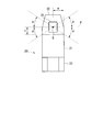
- FIGS. 5A to 5C are diagrams for explaining antenna mounting positions of the antenna module according to the first embodiment of the present invention.
- the antenna 25 is described as an example in which the antenna 25 is omnidirectional in a plane (reference plane P in FIG. 5A) orthogonal to the axis of the casing 21.
- the 3 dB half-value angle of the antenna 25 with respect to the reference plane P that includes the feeding point Q of the antenna 25 and is perpendicular to the axis of the casing 21 is ⁇ , and the outer radius of the casing 21 is ⁇ .
- the outer radius ⁇ of the casing 21 is from the feeding point Q located on the axis of the casing 21 as shown in FIG. 5B. It is the distance to the outer periphery.
- the outer diameter shape of the casing 21 is a square tube shape
- the outer radius ⁇ of the casing 21 passes through the feeding point Q located on the axis of the casing 21 as shown in FIG. 5C. Half the length of the diagonal line.
- the antenna 25 is attached to the above position. That is, when the antenna 25 is attached at a position where the distance between the feeding point Q and the casing 21 is shorter than the shortest distance L, the radio signal is blocked by the casing 21 made of metal, and the performance of the antenna 25 is improved. It will cause a decline. On the other hand, if the antenna 25 is attached at a position where the distance between the feeding point Q and the housing 21 is longer than the shortest distance L, unnecessary radiation increases. For this reason, the antenna is attached to the above position. As long as unnecessary radiation is allowed, the antenna 25 may be attached at a position where the distance between the feeding point Q and the housing 21 is slightly longer than the shortest distance L.
- ⁇ Transmission operation> When a signal is output from the field device FD, this signal is input to the signal processing module 10 via the connection connector CN.
- the signal input to the signal processing module 10 is transmitted to the antenna module 20 by communication between the signal processing module 10 and the antenna module 20 after signal processing such as communication protocol conversion processing is performed.
- the signal transmitted from the signal processing module 10 is sent to the circuit unit 24 of the antenna module 20 via the signal connection terminal T11 of the connector C0, the signal line L11 of the cable CB, and the signal connection terminal T21 of the antenna module 20 shown in FIG. Is input.
- the signal input to the circuit unit 24 is received by the transmission / reception unit 24a shown in FIG. 2 and output to the signal processing unit 24b.
- the signal processing unit 24b performs signal processing such as synchronization processing, data conversion processing, communication protocol conversion processing, encryption processing, and modulation processing on the signal output from the transmission / reception unit 24a.
- the signal subjected to signal processing by the signal processing unit 24b is output to the radio unit 24c.
- the wireless unit 24c performs processing such as synchronization processing, encryption processing, frequency conversion processing, and the like using the signal from the signal processing unit 24b. A radio signal is generated by these processes.
- the radio signal generated by the radio unit 24c is input to the input / output terminal T1 of the transmission / reception switching unit 24d shown in FIG. 3, and the output adjustment unit 31, the filter unit 32, the high-frequency amplifier 33, and the like provided on the transmission path R1, After passing through the output level detector 34 in order, it is output from the input / output terminal T2.
- the switches SW1 and SW2 are switched by the control of the signal processing unit 24b so that the transmission path between the input / output terminals T1 and T2 becomes the transmission path R1.
- the radio signal output from the input / output terminal T2 is input to the feeding point Q of the antenna 25. As a result, a radio signal is transmitted from the antenna 25.
- ⁇ Receive operation> When a radio signal is received by the antenna 25, the radio signal is input to the input / output terminal T2 of the transmission / reception switching unit 24d shown in FIG. 3, and sequentially passes through the bandpass filter 35 and the amplifier 36 provided on the reception path R2. After passing, it is output from the input / output terminal T1.
- the switches SW1 and SW2 are switched by the control of the signal processing unit 24b so that the transmission path between the input / output terminals T1 and T2 becomes the reception path R2.
- the radio signal output from the input / output terminal T1 is input to the radio unit 24c shown in FIG.
- the radio unit 24c performs frequency conversion processing, composite processing, synchronization processing, and the like on the signal output from the transmission / reception switching unit 24d.
- the signal output from the wireless unit 24c is input to the signal processing unit 24b.
- the signal processing unit 24b performs signal processing such as demodulation processing, decoding processing, communication protocol conversion processing, data conversion processing, and synchronization processing on the signal output from the wireless unit 24c.
- the signal subjected to signal processing by the signal processing unit 24b is output to the transmission / reception unit 24a.
- the transmission / reception unit 24 a transmits the signal output from the signal processing unit 24 b toward the signal processing module 10 by communication performed with the signal processing module 10.
- the signal transmitted from the antenna module 20 is input to the signal processing module 10 through the signal connection terminal T21 of the connector unit 23, the signal line L11 of the cable CB, and the signal connection terminal T11 of the connector C0 shown in FIG. .
- the signal input to the signal processing module 10 is transmitted to the field device FD via the connection connector CN after being subjected to signal processing such as communication protocol conversion processing.
- the wireless device 1 is divided into the signal processing module 10 that performs communication with the field device FD and the antenna module 20 that performs wireless communication. Signals exchanged between the modules 20 are transmitted / received via the cable CB.
- the antenna module 20 is configured to accommodate the antenna 25 in the antenna cap 22 so that the wireless signal can be transmitted and received while the periphery of the circuit unit 24 that handles the wireless signal is covered with a cylindrical casing 21.
- FIG. 6 is a diagram schematically showing an antenna module according to the second embodiment of the present invention.
- the antenna module 40 of this embodiment includes a housing 41, an antenna housing portion 42, connector portions 43 a and 43 b, and an antenna 25, and from the signal processing module 10, as with the antenna module 20.
- the transmitted signal is received and transmitted as a radio signal from the antenna 25, and the radio signal received by the antenna 25 is processed and transmitted to the signal processing module 10.
- the antenna 25 is accommodated in the antenna cap 22 provided at one end of the housing 21.
- the antenna 25 is housed in an antenna housing portion 42 provided between both end portions of the housing 41 (between the end portion E1 and the end portion E2).
- the two connector portions 43a and 43b are provided.
- the housing 41 includes two housings 41a and 41b.
- the casings 41a and 41b are cylindrical (cylindrical or polygonal cylindrical) members formed of a highly rigid metal such as high-rigidity aluminum, for example, similarly to the casing 21 of the antenna module 20.
- the circuit part is accommodated so as to cover the periphery of the part (not shown).
- the circuit unit may be housed in either one of the housings 41a and 41b, or may be housed in both the housings 41a and 41b.
- the interiors of the casings 41a and 41b may be filled with resin in order to satisfy the intrinsically safe explosion-proof standard.
- the antenna accommodating portion 42 is a resin member molded in an annular shape or a polygonal annular shape, and has an outer diameter that is approximately the same as the outer diameter of the housings 41a and 41b.
- the antenna 25 is accommodated inside. Similar to the antenna cap 22 shown in FIG. 2, the antenna housing portion 42 is arranged so that the antenna 25 is disposed outside the housing 41 (so that the housing 41 does not cover the periphery of the antenna 25). Accommodate.
- the connector parts 43a and 43b are the same as the connector part 23 shown in FIG. That is, the connector parts 43a and 43b each include a power source connection terminal T20, a signal connection terminal T21, a ground connection terminal T22, and a shell (metal part on the outer periphery) connected to the frame ground FG.
- the two connector portions 43a and 43b are provided in this manner so that the cable CB can be connected from both the upper side (end E1 side) and the lower side (end E2 side) of the antenna module 40. is there.
- One of the connector parts 43a and 43b can be omitted.
- FIG. 7 is a view for explaining an antenna mounting position of the antenna module according to the second embodiment of the present invention.
- the antenna 25 is omnidirectional in the reference plane P
- the 3 dB half-value angle of the antenna 25 with respect to the reference plane P that includes the feeding point Q of the antenna 25 and is orthogonal to the axis of the casing 41 (housing 41a, 41b) is defined as ⁇ .
- the outer radius of 41 is ⁇ .
- the outer radius ⁇ is defined as shown in FIG. 5B when the outer diameter shape of the housing 41 is a cylindrical shape, and when the outer diameter shape of the housing 41 is a square tube shape, the outer radius ⁇ is as shown in FIG. It is defined as shown in
- the antenna 25 is a position where the distance between the feeding point Q in the axial direction of the casing 41 and the end E11 of the casing 41a and the end E12 of the casing 41b is the shortest distance L indicated by the above-described equation (2). Attached to. That is, in the first embodiment, since the antenna 25 is housed in the antenna cap 22 provided at one end of the housing 21, the mounting position of the antenna 25 is determined in consideration of the influence of the housing 21. On the other hand, in the present embodiment, the antenna 25 is housed in the antenna housing portion 42 disposed between the housing 41a and the housing 41b, so that the antenna 25 is taken into consideration by the influence of the housings 41a and 41b. Mounting position is determined. As long as unnecessary radiation can be allowed, the antenna 25 may be attached at a position where the distance between the feeding point Q and at least one of the casings 41a and 41b is slightly longer than the shortest distance L.
- the antenna module 40 of this embodiment differs from the antenna module 20 of the first embodiment only in the mounting position of the antenna 25 and the number of connector portions, and the functions are the same. For this reason, since the freedom degree of an installation place can be raised similarly to the antenna module 20, if the antenna module 20 is installed in a place with a good radio wave state, stable wireless communication can be performed. In addition, since most of the unnecessary radiation radiated from the circuit unit that handles the radio signal of the antenna module 40 is blocked by the casing 41, the unnecessary radiation can be suppressed as much as possible. Thus, also in this embodiment, stable wireless communication can be realized regardless of the installation position of the field device while suppressing unnecessary radiation.
- the present invention is not limited to the above-described embodiment, and can be freely changed within the scope of the present invention. is there.
- the example in which the power source B is provided in the signal processing module 10 and power is supplied from the signal processing module 10 to the antenna module 20 has been described.
- the power supply B of the signal processing module 10 may be omitted, and the power from the field device FD may be supplied to the signal processing module 10 and the antenna module 20.
- the antenna module 20 may be provided with a power source.
- the wireless device 1 is described as measuring the flow rate of fluid as a state quantity in an industrial process.
- the present invention measures other state quantities (for example, pressure, temperature, etc.).
- the present invention can also be applied to wireless devices.
- the wireless device that performs wireless communication conforming to ISA100.11a has been described as an example.
- the present invention is a wireless device that performs wireless communication conforming to WirelessHART (registered trademark), Wi-Fi ( The present invention can also be applied to a wireless device that performs wireless communication conforming to (registered trademark) or a wireless device that performs wireless communication conforming to ZigBee (registered trademark).
Abstract
Description
本願は、2013年9月17日に、日本に出願された特願2013-192339号に基づき優先権を主張し、その内容をここに援用する。 The present invention relates to an antenna module, a wireless device, and a field device control system.
This application claims priority based on Japanese Patent Application No. 2013-192339 filed in Japan on September 17, 2013, the contents of which are incorporated herein by reference.
また、本発明の一態様のアンテナモジュールは、前記回路が、前記第1コネクタを介して外部から送信されてくる信号を受信するとともに、前記第1コネクタを介して外部に信号を送信する送受信回路と、前記送受信回路で受信された信号を無線信号にして前記アンテナから送信させるとともに、前記アンテナで受信された無線信号の処理を行う無線信号処理回路とを備えてもよい。
また、本発明の一態様のアンテナモジュールは、前記第1コネクタが、外部のコネクタを介して前記回路の基準電位を規定するシグナルグランドに接続される第1グランド接続部と、前記外部のコネクタを介して前記筐体の電位を規定するフレームグランドに接続される第2グランド接続部とを備えてもよい。
また、本発明の一態様のアンテナモジュールは、前記第1コネクタが、前記外部のコネクタの信号入出力端に接続される信号接続部と、前記外部のコネクタを介して前記回路の電源に接続される電源接続部とを備えてもよい。
また、本発明の一態様のアンテナモジュールは、前記筐体が、無線信号を遮る物質で形成されてもよい。
また、本発明の一態様のアンテナモジュールは、前記アンテナ収容部が、無線信号を透過する物質で形成されてもよい。
また、本発明の一態様のアンテナモジュールは、前記回路の表層が、樹脂でコーティングされてもよい。
また、本発明の一態様のアンテナモジュールは、前記筐体の内部が、樹脂が充填されてもよい。
また、本発明の一態様のアンテナモジュールは、前記筐体の軸方向における前記アンテナの給電点と前記筐体との最短距離Lは、前記筐体の軸に直交して前記アンテナの給電点が含まれる面を基準とした前記アンテナの3dB半値角をθ、前記筐体の外半径をφとすると、以下の(1)式で表されてもよい。
L=φ×tanθ …(1)
また、本発明の一態様のアンテナモジュールは、前記アンテナが、基板上に形成されたマイクロストリップアンテナであってもよい。
また、本発明の一態様のアンテナモジュールは、前記筐体が、前記アンテナモジュールの第1端部に設けられた第1筐体と、前記第1端部とは反対側の端部である第2端部に設けられた第2筐体とを備え、前記アンテナ及び前記アンテナ収容部は、前記第1筐体と前記第2筐体との間に設けられてもよい。
また、本発明の一態様のアンテナモジュールは、前記第1コネクタが、前記第1筐体及び前記第2筐体の両方に設けられてもよい。
本発明の一態様の無線機器は、フィールド機器との間で信号の送受信を行う信号処理モジュールと、前記信号処理モジュールとの間で信号の送受信を行うアンテナモジュールと、を備え、前記アンテナモジュールは、アンテナと、前記アンテナを用いて無線信号の送受信を行う回路と、前記回路の周囲を覆うように前記回路を収容する筐体と、無線信号の送受信が可能なように前記アンテナを収容するアンテナ収容部と、前記筐体に接合されており、前記回路で送受信される信号を入出力するための第1コネクタとを備える。
また、本発明の一態様の無線機器は、前記信号処理モジュールが、前記アンテナモジュールの前記第1コネクタが直接又はケーブルを介して接続される第2コネクタを備えてもよい。
また、本発明の一態様の無線機器は、前記第1コネクタと、前記第2コネクタとの間を接続するケーブルを更に備えてもよい。
また、本発明の一態様の無線機器は、前記ケーブルが、前記アンテナモジュールに設けられた前記回路の基準電位を規定するシグナルグランドに接続されるグランド線と、前記回路に接続されて前記第1,第2信号の送受信が行われる信号線と、前記回路の電源に接続される電源線と、前記グランド線、前記信号線、及び前記電源線の周囲に設けられ、前記アンテナモジュールの筐体の電位を規定するフレームグランドに接続されるシールドとを備えてもよい。
本発明の一態様のフィールド機器制御システムは、フィールド機器と、前記フィールド機器との間で信号の送受信を行う信号処理モジュールと、前記信号処理モジュールとの間で信号の送受信を行うアンテナモジュールと、を備え、前記アンテナモジュールは、アンテナと、前記アンテナを用いて無線信号の送受信を行う回路と、前記回路の周囲を覆うように前記回路を収容する筐体と、無線信号の送受信が可能なように前記アンテナを収容するアンテナ収容部と、前記筐体に接合されており、前記回路で送受信される信号を入出力するための第1コネクタとを備える。
また、本発明の一態様のフィールド機器制御システムは、前記信号処理モジュールが、前記アンテナモジュールの前記第1コネクタとの間で信号の送受信を行うための第2コネクタを備えてもよい。
また、本発明の一態様のフィールド機器制御システムは、前記第1コネクタと、前記第2コネクタとの間を接続するケーブルを更に備えてもよい。
また、本発明の一態様のフィールド機器制御システムは、前記ケーブルは、前記アンテナモジュールに設けられた前記回路の基準電位を規定するシグナルグランドに接続されるグランド線と、前記回路に接続されて前記フィールド機器との間で信号の送受信が行われる信号線と、前記回路の電源に接続される電源線と、前記グランド線、前記信号線、及び前記電源線の周囲に設けられ、前記アンテナモジュールの筐体の電位を規定するフレームグランドに接続されるシールドとを備えてもよい。 The antenna module of one embodiment of the present invention is capable of transmitting and receiving radio signals, an antenna, a circuit that transmits and receives radio signals using the antenna, a housing that houses the circuits so as to cover the periphery of the circuits In this way, an antenna housing portion that houses the antenna and a first connector that is joined to the housing and that inputs and outputs signals transmitted and received by the circuit.
In the antenna module of one embodiment of the present invention, the circuit receives and transmits a signal transmitted from the outside through the first connector and transmits a signal to the outside through the first connector. And a radio signal processing circuit that converts a signal received by the transmission / reception circuit into a radio signal and transmits the signal from the antenna, and performs processing of the radio signal received by the antenna.
In the antenna module of one embodiment of the present invention, the first connector includes a first ground connection portion that is connected to a signal ground that defines a reference potential of the circuit via an external connector, and the external connector. And a second ground connection portion connected to a frame ground that defines the potential of the casing.
In the antenna module of one embodiment of the present invention, the first connector is connected to a signal connection portion connected to a signal input / output end of the external connector and a power source of the circuit via the external connector. A power supply connection section.
In the antenna module of one embodiment of the present invention, the housing may be formed of a substance that blocks radio signals.
In the antenna module of one embodiment of the present invention, the antenna housing portion may be formed of a material that transmits a radio signal.
In the antenna module of one embodiment of the present invention, the surface layer of the circuit may be coated with a resin.
In the antenna module of one embodiment of the present invention, the inside of the housing may be filled with resin.
In the antenna module of one embodiment of the present invention, the shortest distance L between the feeding point of the antenna and the casing in the axial direction of the casing is perpendicular to the axis of the casing, and the feeding point of the antenna is If the 3 dB half-value angle of the antenna relative to the included plane is θ, and the outer radius of the housing is φ, the following equation (1) may be used.
L = φ × tanθ (1)
In the antenna module of one embodiment of the present invention, the antenna may be a microstrip antenna formed on a substrate.
In the antenna module of one embodiment of the present invention, the housing includes a first housing provided at a first end of the antenna module, and an end opposite to the first end. A second housing provided at two ends, and the antenna and the antenna housing portion may be provided between the first housing and the second housing.
In the antenna module of one embodiment of the present invention, the first connector may be provided in both the first housing and the second housing.
A wireless device of one embodiment of the present invention includes a signal processing module that transmits and receives signals to and from a field device, and an antenna module that transmits and receives signals to and from the signal processing module. An antenna, a circuit that transmits and receives a radio signal using the antenna, a housing that houses the circuit so as to cover the periphery of the circuit, and an antenna that houses the antenna so that radio signal can be transmitted and received The housing includes a housing and a first connector that inputs and outputs signals transmitted and received by the circuit.
In the wireless device of one embodiment of the present invention, the signal processing module may include a second connector to which the first connector of the antenna module is connected directly or via a cable.
The wireless device of one embodiment of the present invention may further include a cable connecting the first connector and the second connector.
In the wireless device of one embodiment of the present invention, the cable is connected to the signal ground that defines a reference potential of the circuit provided in the antenna module and the circuit is connected to the first circuit. , A signal line for transmitting and receiving the second signal, a power line connected to the power source of the circuit, the ground line, the signal line, and the power line, and provided around the antenna module housing. A shield connected to a frame ground that defines the potential may be provided.
A field device control system according to an aspect of the present invention includes a field device, a signal processing module that transmits / receives a signal to / from the field device, an antenna module that transmits / receives a signal to / from the signal processing module, The antenna module is capable of transmitting and receiving radio signals, an antenna, a circuit that transmits and receives radio signals using the antenna, and a housing that houses the circuits so as to cover the periphery of the circuits. And an antenna housing portion for housing the antenna, and a first connector that is joined to the housing and that inputs and outputs signals transmitted and received by the circuit.
In the field device control system of one embodiment of the present invention, the signal processing module may include a second connector for transmitting and receiving signals to and from the first connector of the antenna module.
The field device control system according to one aspect of the present invention may further include a cable connecting the first connector and the second connector.
In the field device control system according to one aspect of the present invention, the cable is connected to a signal ground that defines a reference potential of the circuit provided in the antenna module, and the circuit is connected to the circuit. A signal line for transmitting and receiving signals to and from a field device; a power line connected to a power source of the circuit; and the ground line, the signal line, and the power line. You may provide the shield connected to the frame ground which prescribes | regulates the electric potential of a housing | casing.
図1は、本発明の第1実施形態による無線機器の使用状態の一例を示す図である。図1に示す通り、本実施形態の無線機器1は、信号処理モジュール10とアンテナモジュール20とを備えている。また、無線機器1は、配管PLに取り付けられているフィールド機器FDに接続されて、フィールド機器FDからの信号(第1信号)に基づき生成した無線信号を送信し、無線信号で送信されてくるフィールド機器FDへの信号(第2信号)を受信する。尚、無線機器1は、ISA100.11aに準拠した無線通信を行う。 [First Embodiment]
FIG. 1 is a diagram illustrating an example of a usage state of a wireless device according to the first embodiment of the present invention. As shown in FIG. 1, the
L=φ×tanθ×α …(2) As shown in FIG. 5A, the 3 dB half-value angle of the
L = φ × tan θ × α (2)
フィールド機器FDから信号が出力されると、この信号は接続コネクタCNを介して信号処理モジュール10に入力される。信号処理モジュール10に入力された信号は、通信プロトコルの変換処理等の信号処理が行われた後に、信号処理モジュール10とアンテナモジュール20との間で行われる通信によってアンテナモジュール20に向けて送信される。信号処理モジュール10から送信された信号は、図4に示すコネクタC0の信号接続端子T11、ケーブルCBの信号線L11、及びアンテナモジュール20の信号接続端子T21を順に介してアンテナモジュール20の回路部24に入力される。 <Transmission operation>
When a signal is output from the field device FD, this signal is input to the
アンテナ25で無線信号が受信されると、この無線信号は、図3に示す送受信切替部24dの入出力端T2に入力され、受信経路R2上に設けられたバンドパスフィルタ35及び増幅器36を順に通過した後に入出力端T1から出力される。尚、受信動作時には、信号処理部24bの制御によって、入出力端T1,T2間の伝送経路が受信経路R2となるようにスイッチSW1,SW2が切り替えられている。 <Receive operation>
When a radio signal is received by the
図6は、本発明の第2実施形態によるアンテナモジュールを模式的に示す図である。図6に示す通り、本実施形態のアンテナモジュール40は、筐体41、アンテナ収容部42、コネクタ部43a,43b、及びアンテナ25を備えており、アンテナモジュール20と同様に、信号処理モジュール10から送信されてくる信号を受信してアンテナ25から無線信号にして送信するとともに、アンテナ25で受信した無線信号を処理して信号処理モジュール10に向けて送信する。 [Second Embodiment]
FIG. 6 is a diagram schematically showing an antenna module according to the second embodiment of the present invention. As shown in FIG. 6, the
10 信号処理モジュール
20 アンテナモジュール
21 筐体
22 アンテナキャップ
23 コネクタ部
24 回路部
24a 送受信部
24b 信号処理部
24c 無線部
25 アンテナ
40 アンテナモジュール
41 筐体
42 アンテナ収容部
43a,43b コネクタ部
B 電源
C0 コネクタ
C12 コネクタ
CB ケーブル
FD フィールド機器
FG フレームグランド
L12 グランド線
L10 電源線
L11 信号線
Q 給電点
SD シールド
SG シグナルグランド
T20 電源接続端子
T21 信号接続端子
T22 グランド接続端子 DESCRIPTION OF
Claims (20)
- アンテナと、
前記アンテナを用いて無線信号の送受信を行う回路と、
前記回路の周囲を覆うように前記回路を収容する筐体と、
無線信号の送受信が可能なように前記アンテナを収容するアンテナ収容部と、
前記筐体に接合されており、前記回路で送受信される信号を入出力するための第1コネクタと
を備えるアンテナモジュール。 An antenna,
A circuit for transmitting and receiving radio signals using the antenna;
A housing that houses the circuit so as to cover the periphery of the circuit;
An antenna housing portion for housing the antenna so that wireless signals can be transmitted and received;
An antenna module comprising: a first connector that is joined to the housing and that inputs and outputs signals transmitted and received by the circuit. - 前記回路は、前記第1コネクタを介して外部から送信されてくる信号を受信するとともに、前記第1コネクタを介して外部に信号を送信する送受信回路と、
前記送受信回路で受信された信号を無線信号にして前記アンテナから送信させるとともに、前記アンテナで受信された無線信号の処理を行う無線信号処理回路と
を備える請求項1記載のアンテナモジュール。 The circuit receives a signal transmitted from the outside via the first connector, and transmits / receives a signal to the outside via the first connector;
The antenna module according to claim 1, further comprising: a radio signal processing circuit that converts a signal received by the transmission / reception circuit into a radio signal, transmits the radio signal from the antenna, and processes the radio signal received by the antenna. - 前記第1コネクタは、外部のコネクタを介して前記回路の基準電位を規定するシグナルグランドに接続される第1グランド接続部と、
前記外部のコネクタを介して前記筐体の電位を規定するフレームグランドに接続される第2グランド接続部と
を備える請求項1又は請求項2記載のアンテナモジュール。 The first connector is connected to a signal ground that defines a reference potential of the circuit via an external connector;
The antenna module according to claim 1, further comprising: a second ground connection portion connected to a frame ground that defines a potential of the housing via the external connector. - 前記第1コネクタは、前記外部のコネクタの信号入出力端に接続される信号接続部と、
前記外部のコネクタを介して前記回路の電源に接続される電源接続部と
を備える請求項3記載のアンテナモジュール。 The first connector includes a signal connection portion connected to a signal input / output end of the external connector;
The antenna module according to claim 3, further comprising: a power supply connection portion connected to a power supply of the circuit via the external connector. - 前記筐体は、無線信号を遮る物質で形成されている請求項1から請求項4の何れか一項に記載のアンテナモジュール。 The antenna module according to any one of claims 1 to 4, wherein the casing is formed of a substance that blocks radio signals.
- 前記アンテナ収容部は、無線信号を透過する物質で形成されている請求項1から請求項5の何れか一項に記載のアンテナモジュール。 The antenna module according to any one of claims 1 to 5, wherein the antenna housing portion is formed of a material that transmits a radio signal.
- 前記回路の表層は、樹脂でコーティングされている請求項1から請求項6の何れか一項に記載のアンテナモジュール。 The antenna module according to any one of claims 1 to 6, wherein a surface layer of the circuit is coated with a resin.
- 前記筐体の内部は、樹脂が充填されている請求項1から請求項6の何れか一項に記載のアンテナモジュール。 The antenna module according to any one of claims 1 to 6, wherein the inside of the housing is filled with resin.
- 前記筐体の軸方向における前記アンテナの給電点と前記筐体との最短距離Lは、前記筐体の軸に直交して前記アンテナの給電点が含まれる面を基準とした前記アンテナの3dB半値角をθ、前記筐体の外半径をφとすると、以下の(1)式で表される請求項1から請求項8の何れか一項に記載のアンテナモジュール。
L=φ×tanθ …(1) The shortest distance L between the feeding point of the antenna and the housing in the axial direction of the housing is a 3 dB half value of the antenna with respect to a plane perpendicular to the housing axis and including the feeding point of the antenna. The antenna module according to any one of claims 1 to 8, represented by the following expression (1), where θ is an angle and φ is an outer radius of the housing.
L = φ × tanθ (1) - 前記アンテナは、基板上に形成されたマイクロストリップアンテナである請求項1から請求項9の何れか一項に記載のアンテナモジュール。 The antenna module according to any one of claims 1 to 9, wherein the antenna is a microstrip antenna formed on a substrate.
- 前記筐体は、前記アンテナモジュールの第1端部に設けられた第1筐体と、前記第1端部とは反対側の端部である第2端部に設けられた第2筐体とを備え、
前記アンテナ及び前記アンテナ収容部は、前記第1筐体と前記第2筐体との間に設けられる請求項1から請求項10の何れか一項に記載のアンテナモジュール。 The casing includes a first casing provided at a first end of the antenna module, and a second casing provided at a second end that is an end opposite to the first end. With
The antenna module according to any one of claims 1 to 10, wherein the antenna and the antenna housing portion are provided between the first housing and the second housing. - 前記第1コネクタは、前記第1筐体及び前記第2筐体の両方に設けられる請求項11に記載のアンテナモジュール。 The antenna module according to claim 11, wherein the first connector is provided in both the first casing and the second casing.
- フィールド機器との間で信号の送受信を行う信号処理モジュールと、
前記信号処理モジュールとの間で信号の送受信を行うアンテナモジュールと、を備え、
前記アンテナモジュールは、
アンテナと、
前記アンテナを用いて無線信号の送受信を行う回路と、
前記回路の周囲を覆うように前記回路を収容する筐体と、
無線信号の送受信が可能なように前記アンテナを収容するアンテナ収容部と、
前記筐体に接合されており、前記回路で送受信される信号を入出力するための第1コネクタと
を備える無線機器。 A signal processing module that transmits and receives signals to and from field devices;
An antenna module for transmitting and receiving signals to and from the signal processing module,
The antenna module is
An antenna,
A circuit for transmitting and receiving radio signals using the antenna;
A housing that houses the circuit so as to cover the periphery of the circuit;
An antenna housing portion for housing the antenna so that wireless signals can be transmitted and received;
A wireless device comprising: a first connector that is joined to the housing and that inputs and outputs signals transmitted and received by the circuit. - 前記信号処理モジュールは、前記アンテナモジュールの前記第1コネクタとの間で信号の送受信を行うための第2コネクタを備える請求項13記載の無線機器。 The wireless device according to claim 13, wherein the signal processing module includes a second connector for transmitting and receiving signals to and from the first connector of the antenna module.
- 前記第1コネクタと、前記第2コネクタとの間を接続するケーブルを更に備える請求項14記載の無線機器。 The wireless device according to claim 14, further comprising a cable connecting the first connector and the second connector.
- 前記ケーブルは、前記アンテナモジュールに設けられた前記回路の基準電位を規定するシグナルグランドに接続されるグランド線と、
前記回路に接続されて前記フィールド機器との間で信号の送受信が行われる信号線と、
前記回路の電源に接続される電源線と、
前記グランド線、前記信号線、及び前記電源線の周囲に設けられ、前記アンテナモジュールの筐体の電位を規定するフレームグランドに接続されるシールドと
を備える請求項15記載の無線機器。 The cable includes a ground line connected to a signal ground that defines a reference potential of the circuit provided in the antenna module;
A signal line connected to the circuit for transmitting and receiving signals to and from the field device;
A power line connected to the power source of the circuit;
The wireless device according to claim 15, further comprising: a shield provided around the ground line, the signal line, and the power supply line, and connected to a frame ground that defines a potential of the casing of the antenna module. - フィールド機器と、
前記フィールド機器との間で信号の送受信を行う信号処理モジュールと、
前記信号処理モジュールとの間で信号の送受信を行うアンテナモジュールと、を備え、
前記アンテナモジュールは、
アンテナと、
前記アンテナを用いて無線信号の送受信を行う回路と、
前記回路の周囲を覆うように前記回路を収容する筐体と、
無線信号の送受信が可能なように前記アンテナを収容するアンテナ収容部と、
前記筐体に接合されており、前記回路で送受信される信号を入出力するための第1コネクタと
を備えるフィールド機器制御システム。 Field equipment,
A signal processing module for transmitting and receiving signals to and from the field device;
An antenna module for transmitting and receiving signals to and from the signal processing module,
The antenna module is
An antenna,
A circuit for transmitting and receiving radio signals using the antenna;
A housing that houses the circuit so as to cover the periphery of the circuit;
An antenna housing portion for housing the antenna so that wireless signals can be transmitted and received;
A field device control system comprising: a first connector that is joined to the housing and that inputs and outputs signals transmitted and received by the circuit. - 前記信号処理モジュールは、前記アンテナモジュールの前記第1コネクタとの間で信号の送受信を行うための第2コネクタを備える請求項17記載のフィールド機器制御システム。 The field device control system according to claim 17, wherein the signal processing module includes a second connector for transmitting and receiving signals to and from the first connector of the antenna module.
- 前記第1コネクタと、前記第2コネクタとの間を接続するケーブルを更に備える請求項18記載のフィールド機器制御システム。 The field device control system according to claim 18, further comprising a cable connecting between the first connector and the second connector.
- 前記ケーブルは、前記アンテナモジュールに設けられた前記回路の基準電位を規定するシグナルグランドに接続されるグランド線と、
前記回路に接続されて前記フィールド機器との間で信号の送受信が行われる信号線と、
前記回路の電源に接続される電源線と、
前記グランド線、前記信号線、及び前記電源線の周囲に設けられ、前記アンテナモジュールの筐体の電位を規定するフレームグランドに接続されるシールドと
を備える請求項19記載のフィールド機器制御システム。 The cable includes a ground line connected to a signal ground that defines a reference potential of the circuit provided in the antenna module;
A signal line connected to the circuit for transmitting and receiving signals to and from the field device;
A power line connected to the power source of the circuit;
The field device control system according to claim 19, further comprising: a shield provided around the ground line, the signal line, and the power line, and connected to a frame ground that defines a potential of the casing of the antenna module.
Priority Applications (3)
| Application Number | Priority Date | Filing Date | Title |
|---|---|---|---|
| CN201480050742.3A CN105531939B (en) | 2013-09-17 | 2014-09-01 | Anneta module, wireless instruments and field instrumentation control system |
| US14/916,796 US10033426B2 (en) | 2013-09-17 | 2014-09-01 | Antenna module, wireless device, and field device control system |
| EP14845579.3A EP3048740B1 (en) | 2013-09-17 | 2014-09-01 | Antenna module, wireless device, and field-device control system |
Applications Claiming Priority (2)
| Application Number | Priority Date | Filing Date | Title |
|---|---|---|---|
| JP2013-192339 | 2013-09-17 | ||
| JP2013192339A JP5850015B2 (en) | 2013-09-17 | 2013-09-17 | Antenna module and wireless device |
Publications (1)
| Publication Number | Publication Date |
|---|---|
| WO2015041032A1 true WO2015041032A1 (en) | 2015-03-26 |
Family
ID=52688686
Family Applications (1)
| Application Number | Title | Priority Date | Filing Date |
|---|---|---|---|
| PCT/JP2014/072891 WO2015041032A1 (en) | 2013-09-17 | 2014-09-01 | Antenna module, wireless device, and field-device control system |
Country Status (5)
| Country | Link |
|---|---|
| US (1) | US10033426B2 (en) |
| EP (1) | EP3048740B1 (en) |
| JP (1) | JP5850015B2 (en) |
| CN (1) | CN105531939B (en) |
| WO (1) | WO2015041032A1 (en) |
Cited By (1)
| Publication number | Priority date | Publication date | Assignee | Title |
|---|---|---|---|---|
| JP2018074347A (en) * | 2016-10-28 | 2018-05-10 | 横河電機株式会社 | Antenna module |
Families Citing this family (6)
| Publication number | Priority date | Publication date | Assignee | Title |
|---|---|---|---|---|
| JP2017101719A (en) * | 2015-11-30 | 2017-06-08 | 株式会社ボルテックス | Electromagnetic valve system, socket and electromagnetic valve |
| JP6706424B2 (en) * | 2017-02-09 | 2020-06-10 | 横河電機株式会社 | Withstand voltage input intrinsically safe output transmitter |
| WO2019039598A1 (en) * | 2017-08-24 | 2019-02-28 | 株式会社Nttドコモ | Antenna device, wireless base station, and antenna device container |
| JP7027831B2 (en) | 2017-11-16 | 2022-03-02 | 横河電機株式会社 | Wireless device |
| TWI662740B (en) * | 2018-01-09 | 2019-06-11 | 和碩聯合科技股份有限公司 | External antenna and wireless coummunication system |
| WO2020049744A1 (en) * | 2018-09-07 | 2020-03-12 | Smc株式会社 | Wireless antenna module and wireless system |
Citations (11)
| Publication number | Priority date | Publication date | Assignee | Title |
|---|---|---|---|---|
| JP2000004533A (en) * | 1998-06-15 | 2000-01-07 | Mitsubishi Electric Corp | Explosion-proof base station device |
| JP2001144388A (en) * | 1999-11-16 | 2001-05-25 | Denso Corp | Circuit board |
| JP2003308931A (en) * | 2002-04-16 | 2003-10-31 | Mitsubishi Electric Corp | Shield cover for connector |
| JP2004343265A (en) * | 2003-05-14 | 2004-12-02 | Nec Saitama Ltd | Mobile communication terminal |
| JP2006086808A (en) * | 2004-09-16 | 2006-03-30 | Kyocera Corp | Antenna module |
| JP2007036988A (en) * | 2005-07-29 | 2007-02-08 | Tdk Corp | Radio transceiver |
| US20080211664A1 (en) | 2004-04-23 | 2008-09-04 | Reinhard Griech | Radio Module for Field Devices of Automation Technology |
| JP2009146962A (en) * | 2007-12-12 | 2009-07-02 | Panasonic Corp | Noise reduction circuit |
| JP2011146955A (en) * | 2010-01-15 | 2011-07-28 | Fujitsu Toshiba Mobile Communications Ltd | Portable terminal |
| JP2011525330A (en) * | 2008-06-17 | 2011-09-15 | ローズマウント インコーポレイテッド | Improved shape elements and electromagnetic interference protection for process equipment wireless adapters |
| JP2013504207A (en) * | 2009-09-02 | 2013-02-04 | ローズマウント インコーポレイテッド | Wireless process communication adapter with improved encapsulation |
Family Cites Families (21)
| Publication number | Priority date | Publication date | Assignee | Title |
|---|---|---|---|---|
| US5970393A (en) * | 1997-02-25 | 1999-10-19 | Polytechnic University | Integrated micro-strip antenna apparatus and a system utilizing the same for wireless communications for sensing and actuation purposes |
| EP1244174A1 (en) * | 2001-03-20 | 2002-09-25 | Sony International (Europe) GmbH | Mobile terminal with hole in patch antenna |
| US7109948B2 (en) * | 2001-11-20 | 2006-09-19 | Ube Industries, Ltd. | Dielectric antenna module |
| US8060167B2 (en) * | 2002-07-19 | 2011-11-15 | Panasonic Corporation | Portable wireless machine |
| JP2006114941A (en) | 2004-10-12 | 2006-04-27 | Pioneer Electronic Corp | Audio apparatus provided with am broadcast wave reception function |
| TWM288957U (en) * | 2005-11-08 | 2006-03-21 | Compal Electronics Inc | Wireless communication module of portable electronic device |
| KR100758991B1 (en) * | 2006-02-03 | 2007-09-17 | 삼성전자주식회사 | Mobile device having a rfid system |
| US8502739B2 (en) * | 2007-06-22 | 2013-08-06 | Nokia Corporation | Antenna arrangement |
| KR20090065345A (en) * | 2007-12-17 | 2009-06-22 | 현대자동차주식회사 | Expandable and contractable integrated type antenna |
| KR20090119063A (en) * | 2008-05-15 | 2009-11-19 | 삼성전자주식회사 | Antenna module, display device having the same and information processing system having the display device |
| US8270925B2 (en) * | 2008-12-04 | 2012-09-18 | Broadcom Corporation | Extended antenna module and applications thereof |
| US8649825B2 (en) | 2010-07-30 | 2014-02-11 | Blackberry Limited | Mobile wireless communications device with spatial diversity antenna and related methods |
| TW201235848A (en) * | 2011-02-24 | 2012-09-01 | Asustek Comp Inc | Portable electronic device and controlling method thereof |
| US9405285B2 (en) | 2011-03-18 | 2016-08-02 | Honeywell International Inc. | Interface for local configuration and monitoring of an industrial field device with support for provisioning onto an industrial wireless network and related system and method |
| US9391568B2 (en) * | 2011-05-16 | 2016-07-12 | Rosemount Inc. | Process device with light change triggered display |
| US9804647B2 (en) * | 2012-01-06 | 2017-10-31 | Fisher Controls International Llc | Continuously powered field device |
| JP5573885B2 (en) * | 2012-04-27 | 2014-08-20 | 横河電機株式会社 | Self-diagnosis circuit |
| US9518852B2 (en) * | 2012-09-27 | 2016-12-13 | Rosemount Inc. | Hybrid power module with fault detection |
| US9291684B2 (en) * | 2013-06-28 | 2016-03-22 | Rosemount, Inc. | Logic capable power module |
| US11073805B2 (en) * | 2014-11-21 | 2021-07-27 | Fisher-Rosemount Systems, Inc. | Process plant network with secured external access |
| DE102014118617A1 (en) * | 2014-12-15 | 2016-06-16 | Endress+Hauser Process Solutions Ag | Expansion device for a wireless antenna |
-
2013
- 2013-09-17 JP JP2013192339A patent/JP5850015B2/en active Active
-
2014
- 2014-09-01 WO PCT/JP2014/072891 patent/WO2015041032A1/en active Application Filing
- 2014-09-01 CN CN201480050742.3A patent/CN105531939B/en active Active
- 2014-09-01 US US14/916,796 patent/US10033426B2/en active Active
- 2014-09-01 EP EP14845579.3A patent/EP3048740B1/en active Active
Patent Citations (11)
| Publication number | Priority date | Publication date | Assignee | Title |
|---|---|---|---|---|
| JP2000004533A (en) * | 1998-06-15 | 2000-01-07 | Mitsubishi Electric Corp | Explosion-proof base station device |
| JP2001144388A (en) * | 1999-11-16 | 2001-05-25 | Denso Corp | Circuit board |
| JP2003308931A (en) * | 2002-04-16 | 2003-10-31 | Mitsubishi Electric Corp | Shield cover for connector |
| JP2004343265A (en) * | 2003-05-14 | 2004-12-02 | Nec Saitama Ltd | Mobile communication terminal |
| US20080211664A1 (en) | 2004-04-23 | 2008-09-04 | Reinhard Griech | Radio Module for Field Devices of Automation Technology |
| JP2006086808A (en) * | 2004-09-16 | 2006-03-30 | Kyocera Corp | Antenna module |
| JP2007036988A (en) * | 2005-07-29 | 2007-02-08 | Tdk Corp | Radio transceiver |
| JP2009146962A (en) * | 2007-12-12 | 2009-07-02 | Panasonic Corp | Noise reduction circuit |
| JP2011525330A (en) * | 2008-06-17 | 2011-09-15 | ローズマウント インコーポレイテッド | Improved shape elements and electromagnetic interference protection for process equipment wireless adapters |
| JP2013504207A (en) * | 2009-09-02 | 2013-02-04 | ローズマウント インコーポレイテッド | Wireless process communication adapter with improved encapsulation |
| JP2011146955A (en) * | 2010-01-15 | 2011-07-28 | Fujitsu Toshiba Mobile Communications Ltd | Portable terminal |
Cited By (1)
| Publication number | Priority date | Publication date | Assignee | Title |
|---|---|---|---|---|
| JP2018074347A (en) * | 2016-10-28 | 2018-05-10 | 横河電機株式会社 | Antenna module |
Also Published As
| Publication number | Publication date |
|---|---|
| CN105531939A (en) | 2016-04-27 |
| CN105531939B (en) | 2018-03-16 |
| US20160204824A1 (en) | 2016-07-14 |
| JP2015061134A (en) | 2015-03-30 |
| EP3048740A1 (en) | 2016-07-27 |
| US10033426B2 (en) | 2018-07-24 |
| EP3048740B1 (en) | 2020-01-08 |
| JP5850015B2 (en) | 2016-02-03 |
| EP3048740A4 (en) | 2017-04-05 |
Similar Documents
| Publication | Publication Date | Title |
|---|---|---|
| JP5850015B2 (en) | Antenna module and wireless device | |
| RU2467373C2 (en) | Improved form factor and electromagnetic interference protection for process device wireless adapters | |
| WO2015045737A1 (en) | Wireless module, wireless apparatus, and field apparatus control system | |
| US20090081963A1 (en) | Wireless communication device with internal antenna system for use in hazardous locations | |
| JP6241455B2 (en) | Wireless equipment | |
| JP5228040B2 (en) | Link-connected antenna system for mounting on a field device having a grounded housing | |
| WO2014188769A1 (en) | Radio devices and interface module | |
| WO2018079609A1 (en) | Antenna module | |
| KR101652713B1 (en) | Communication cable protection equipment for building | |
| EP3407551B1 (en) | Wireless gateway system and communication method thereof |
Legal Events
| Date | Code | Title | Description |
|---|---|---|---|
| WWE | Wipo information: entry into national phase |
Ref document number: 201480050742.3 Country of ref document: CN |
|
| 121 | Ep: the epo has been informed by wipo that ep was designated in this application |
Ref document number: 14845579 Country of ref document: EP Kind code of ref document: A1 |
|
| REEP | Request for entry into the european phase |
Ref document number: 2014845579 Country of ref document: EP |
|
| WWE | Wipo information: entry into national phase |
Ref document number: 2014845579 Country of ref document: EP |
|
| WWE | Wipo information: entry into national phase |
Ref document number: 14916796 Country of ref document: US |
|
| NENP | Non-entry into the national phase |
Ref country code: DE |