WO2015016023A1 - 撮像モジュール及び電子機器並びに撮像モジュールの製造方法 - Google Patents
撮像モジュール及び電子機器並びに撮像モジュールの製造方法 Download PDFInfo
- Publication number
- WO2015016023A1 WO2015016023A1 PCT/JP2014/068251 JP2014068251W WO2015016023A1 WO 2015016023 A1 WO2015016023 A1 WO 2015016023A1 JP 2014068251 W JP2014068251 W JP 2014068251W WO 2015016023 A1 WO2015016023 A1 WO 2015016023A1
- Authority
- WO
- WIPO (PCT)
- Prior art keywords
- imaging module
- lens
- unit
- imaging
- image sensor
- Prior art date
- Legal status (The legal status is an assumption and is not a legal conclusion. Google has not performed a legal analysis and makes no representation as to the accuracy of the status listed.)
- Ceased
Links
Images




Classifications
-
- G—PHYSICS
- G02—OPTICS
- G02B—OPTICAL ELEMENTS, SYSTEMS OR APPARATUS
- G02B7/00—Mountings, adjusting means, or light-tight connections, for optical elements
- G02B7/02—Mountings, adjusting means, or light-tight connections, for optical elements for lenses
- G02B7/04—Mountings, adjusting means, or light-tight connections, for optical elements for lenses with mechanism for focusing or varying magnification
- G02B7/08—Mountings, adjusting means, or light-tight connections, for optical elements for lenses with mechanism for focusing or varying magnification adapted to co-operate with a remote control mechanism
-
- H—ELECTRICITY
- H04—ELECTRIC COMMUNICATION TECHNIQUE
- H04N—PICTORIAL COMMUNICATION, e.g. TELEVISION
- H04N23/00—Cameras or camera modules comprising electronic image sensors; Control thereof
- H04N23/50—Constructional details
-
- H—ELECTRICITY
- H04—ELECTRIC COMMUNICATION TECHNIQUE
- H04N—PICTORIAL COMMUNICATION, e.g. TELEVISION
- H04N23/00—Cameras or camera modules comprising electronic image sensors; Control thereof
- H04N23/57—Mechanical or electrical details of cameras or camera modules specially adapted for being embedded in other devices
-
- H—ELECTRICITY
- H04—ELECTRIC COMMUNICATION TECHNIQUE
- H04N—PICTORIAL COMMUNICATION, e.g. TELEVISION
- H04N23/00—Cameras or camera modules comprising electronic image sensors; Control thereof
- H04N23/60—Control of cameras or camera modules
- H04N23/66—Remote control of cameras or camera parts, e.g. by remote control devices
Definitions
- the present invention relates to an imaging module, an electronic device, and a manufacturing method of the imaging module.
- An imaging module having an autofocus function and an image blur correction function is known as an imaging module mounted on a portable electronic device such as a mobile phone (see, for example, Patent Documents 1 and 2).
- An imaging module described in Patent Document 1 is an imaging module having an image blur correction function, and a unit in which a lens group and an imaging element are integrated, and a lens that swings the lens group and the imaging element unit. And a driving device, and is configured to prevent image blur by swinging the unit of the lens and the image sensor.
- the lens driving device is connected to a terminal portion provided on a flexible substrate connected to the image pickup device via the flexible substrate, and is operated by being supplied with electric power or the like via both flexible substrates.
- the imaging module described in Patent Document 2 is an imaging module having an autofocus function and an image shake correction function, and includes an imaging element unit having an imaging element, a lens group, and a lens driving device that displaces the lens group. And a lens unit that is bonded and fixed to the image sensor unit, and is configured to adjust the focus by adjusting the position of the lens group by a lens driving device and to prevent image blurring.
- the lens driving device is connected to a terminal portion provided on the substrate of the imaging element unit via a flexible substrate, and is operated by being supplied with electric power or the like via the substrate of the imaging element unit and the flexible substrate.
- the image sensor unit or the lens unit is arranged at different positions in the optical axis direction of the lens group, and Then, the relative position and relative orientation of both units are calculated from a plurality of images obtained by imaging the measurement chart, and the relative position and relative orientation between the lens unit and the image sensor unit are calculated according to the calculated adjustment amount.
- a method is also known in which both units are bonded and fixed in an adjusted state (see Patent Document 3).
- the flexible connected to the lens driving device of the lens unit is completed.
- the substrate is connected to a terminal portion provided on the substrate of the image sensor unit. Therefore, the lens driving device cannot be operated via the substrate of the image sensor unit and the flexible substrate when adjusting the relative position and relative attitude between the image sensor unit and the lens unit.
- An object of the present invention is to make it possible to easily and accurately adjust the relative position and relative orientation between an image sensor unit and a lens unit.
- Focus adjustment and image blur correction by moving an image sensor unit having a circuit provided with an image sensor and an external connection unit, a lens group, and at least a part of lenses of the lens group with respect to the image sensor.
- a lens unit that is fixed to the imaging element unit, and a wiring group that connects the lens driving device to the circuit, and the wiring group includes at least one wiring path.
- the imaging module further comprising a plurality of flexible wiring portions that are divided into a plurality of wiring sets in the section and are provided for each of the wiring sets and separated from each other.
- the lens unit and the imaging element unit set on the Z axis orthogonal to the measurement chart, and any one of the measurement charts are set to a plurality of measurement positions.
- a plurality of measurement chart images formed by the lens unit are captured by the imaging element while the lens driving device is operated through the external connection unit.
- the lens unit around the X axis and the Y axis perpendicular to the Z axis and the relative position between the lens unit and the imaging element unit on the Z axis based on the acquired plurality of images And an adjustment amount of the relative orientation between the lens unit and the image sensor unit, and the lens unit and the image sensor unit based on the obtained adjustment amount.
- a method of manufacturing an imaging module that adjusts the relative position and the relative attitude with respect to a camera and fixes the lens unit and the imaging element unit in which the relative position and the relative attitude are adjusted.
- the lens unit and the imaging element unit set on the Z axis orthogonal to the measurement chart, and any one of the measurement charts are set to a plurality of measurement positions.
- a plurality of measurement chart images formed by the lens unit are captured by the imaging element while the lens driving device is operated through the wiring group.
- An image is acquired, and based on the acquired plurality of images, a relative position between the lens unit and the imaging element unit on the Z axis, and the lens unit around the X axis and the Y axis orthogonal to the Z axis, An adjustment amount of a relative posture with respect to the image sensor unit is obtained, and the lens unit and the image sensor unit are based on the obtained adjustment amount. Adjusting the relative position and the relative attitude of the lens, fixing the lens unit and the image sensor unit adjusted in the relative position and the relative attitude, and connecting the wiring group to the circuit of the image sensor unit. Manufacturing method of imaging module.
- the relative position and orientation of the image sensor unit and the lens unit can be easily and accurately adjusted.
- FIG. 2 is a plan view of a flexible substrate for wiring a wiring group that connects a lens driving device of a lens unit and a circuit of an imaging element unit in the imaging module of FIG. 1.
- FIG. 3 is a flowchart of a manufacturing process of the imaging module 1.
- FIG. 3 is a schematic diagram of the other example of an imaging module for describing embodiment of this invention.
- FIG. 1 shows an external appearance of an example of an imaging module for explaining an embodiment of the present invention
- FIG. 2 shows a cross section of the imaging module of FIG.
- the imaging module 1 includes a lens unit 2 and an imaging element unit 3 to which the lens unit 2 is fixed.
- the lens unit 2 includes a lens group 10, a lens driving device 11, and a flexible substrate 12.
- the lens group 10 is housed in a cylindrical lens barrel 13 and is integrally supported by the lens barrel 13.
- the lens group 10 includes four lenses 10A, 10B, 10C, and 10D in the illustrated example, but the number of lenses is not limited to four.
- the lens driving device 11 performs focus adjustment for moving the lens barrel 13 supporting the lens group 10 along the lens optical axis Az. Further, the lens driving device 11 performs image blur correction for moving the lens barrel 13 along a plane perpendicular to the lens optical axis Az.
- the lens barrel 13 may be configured to perform image blur correction by tilting the lens barrel 13 with respect to a plane perpendicular to the lens optical axis Az. Further, it may be configured to perform focus adjustment and image blur correction by moving some of the lenses in the lens group 10.
- the lens group 10, the lens barrel 13, and the lens driving device 11 are accommodated in a casing 14, and an opening opened at the bottom of the casing 14 between the lens barrel 13 and the casing 14 is blocked by a bottom block 15. ing.
- the flexible substrate 12 is a signal (including electric power) for operating the lens driving device 11. It is comprised including the wiring group which transmits.
- the image sensor unit 3 includes an image sensor 20 and a circuit provided with an external connection unit 21.
- the image pickup device 20 is an image pickup device such as a CCD (Charge-Coupled Device) image sensor or a CMOS (Complementary Metal-Oxide-Semiconductor) image sensor, and is an image pickup device having a relatively high number of pixels, for example, 3 to 10 million pixels.
- CCD Charge-Coupled Device
- CMOS Complementary Metal-Oxide-Semiconductor
- the imaging element 20 is mounted on an element fixing substrate 22 and covered with a cover glass 23.
- the cover glass 23 is supported by the cover holder 24 and disposed on the element fixing substrate 22.
- the circuit provided in the imaging element unit 3 is a circuit for operating the imaging device 20 and the lens driving device 11 of the lens unit 2, and is provided on the element fixing substrate 22 and the flexible substrate 25 extended from the element fixing substrate 22. It has been.
- the external connection unit 21 is for connecting the circuit of the image sensor unit 3 to the circuit of the external device, and is provided at the tip of the flexible substrate 25 in the illustrated example.
- the flexible substrate 25 is provided with a connection portion 26 to which the flexible substrate 12 of the lens unit 2 is connected.
- the lens driving device 11 of the lens unit 2 is connected to the circuit of the imaging element unit 3 via a wiring group included in the flexible substrate 12.
- the lens unit 2 is assembled to the image sensor unit 3 in a state where the image plane of the lens group 10 coincides with the image receiving surface of the image sensor 20, and is fixed in that state.
- the lens unit 2 and the image sensor unit 3 are fixed by, for example, bonding the housing 14 or the bottom block 15 of the lens unit 2 to the element fixing substrate 22 or the cover holder 24 of the image sensor unit 3.
- FIG. 3 shows functional blocks of the imaging module 1.
- the lens driving device 11 of the lens unit 2 includes an actuator 30z that moves the lens barrel 13 along the lens optical axis Az, and the lens barrel 13 of the orthogonal two axes Ax and Ay in the plane perpendicular to the lens optical axis Az.
- the actuator 30x moves along the axial direction
- the actuator 30y moves the lens barrel 13 along the Ay axial direction.
- the lens driving device 11 includes a position sensor 31x that detects the position of the lens barrel 13 in the Ax axis direction, a position sensor 31y that detects the position of the lens barrel 13 in the Ay axis direction, and the Az axis direction of the lens barrel 13 in the Az axis direction. And a position sensor 31z for detecting the position.
- the circuit of the imaging device unit 3 includes an angular velocity sensor 32x that detects an angular velocity around the Ax axis that acts on the imaging module 1, an angular velocity sensor 32y that detects an angular velocity around the Ay axis that acts on the imaging module 1, and an actuator 30x, A control IC (Integrated Circuit) 34 for driving 30y and 30z is provided.
- the control IC 34 calculates the amount of movement of the lens barrel 13 in the Az axis direction for focus adjustment based on the position signal output from the position sensor 31z and the image signal output from the image sensor 20. Further, the control IC 34 is based on the angular velocity signals output from the angular velocity sensors 32x and 32y and the position signals output from the position sensors 31x and 31y, in the Ax axis direction and the Ay axis direction of the lens barrel 13 for image blur correction. The amount of movement is calculated. The control IC 34 controls the actuators 30x, 30y, and 30z based on the calculated movement amounts in the respective directions.
- the operating power of the angular velocity sensors 32 x and 32 y and the control IC 34 is supplied from an external device connected to the external connection portion 21 of the image sensor unit 3.
- the operating power of the actuators 30x, 30y, 30z and the position sensors 31x, 31y, 31z is supplied from the control IC 34.
- the wiring for transmitting the operating power is indicated by a thick solid line
- the wiring for transmitting the position signal is indicated by a thin solid line.
- VCMs voice coil motors
- hall elements are used in the illustrated example, and typically four wires are required for each hall element. Therefore, the flexible substrate 12 includes a large number of wirings.
- the angular velocity sensors 32x and 32y and the control IC 34 are all provided in the image pickup device unit 3.
- the control IC 34 may be provided in the lens unit 2, and in this case, the control IC 34 is provided.
- the wiring that transmits the operating power of the control IC 34, the image signal output from the image sensor 20, and the angular velocity Wiring for transmitting the angular velocity signals output from the sensors 32 x and 32 y to the control IC 34 is included in the flexible substrate 12.
- the wiring group included in the flexible substrate 12 is divided into a plurality of wiring groups in at least a part of the wiring path, and a flexible wiring part configured flexibly for each wiring group is provided.
- FIG. 4 shows a plan view of the flexible substrate 12.
- the flexible substrate 12 has a housing area A1 that is housed in the housing 14 of the lens unit 2 and a lead-out area A2 that is led out of the housing 14.
- a circular hole 40 through which the lens barrel 13 is inserted is formed in the housing area A1.
- the housing area A1 is disposed so as to surround the outer periphery of the lens barrel 13 and is connected to the lens driving device 11 that is also disposed on the outer periphery of the lens barrel 13.
- the accommodation area A1 is formed with a slit 41 connected to the circular hole 40, and two partial substrates 12a-1 and 12a-2 that are separated by the slit 41 and parallel to each other are provided.
- the lead-out area A2 is led out from the side surface of the casing 14 facing in the Ay axis direction facing the external connection portion 21 of the image pickup device unit 3 from the case 14 of the lens unit 2 toward the external connection portion 21, and the image pickup device unit. 3 connection part 26 (refer FIG. 1).
- the partial boards 12a-1 and 12a-2 include wiring sets W1 and W2 configured by distributing the wiring group W wired by the flexible board 12 into two sets, respectively, and are provided for each of the wiring sets W1 and W2.
- the flexible wiring portion is configured.
- the flexible wiring portions 12a-1 and 12a-2 extend in parallel to each other in the derivation direction (Ay axis direction) of the derivation region A2.
- the flexible wiring portion 12a-1 is provided in one of the two regions divided in the Ax axis direction by the center plane C that is a surface including the lens optical axes Az and Ay axes along the surface.
- the flexible wiring portion 12a-2 is provided in the other of the two regions divided in the Ax axis direction by the center plane C.
- the flexible wiring portions 12a-1 and 12a-2 are provided on both sides of the center plane C. More specifically, the flexible wiring portions 12a-1 and 12a-2 are provided symmetrically with respect to the center plane C.
- the slit 41 separating the flexible wiring portions 12a-1 and 12a-2 may be, for example, a cut, but in the illustrated example, it is formed as a rectangular hole, and the flexible wiring portions 12a-1 and 12a- There is a space between the two. That is, the flexible wiring portions 12a-1 and 12a-2 are arranged with a space therebetween.
- the wiring group W can be divided into a plurality of wiring groups.
- the wiring for transmitting the position signal may be a set, and the wiring for transmitting the operating power to each of the actuators 30x, 30y, 30z may be a set.
- the number of wiring groups is not limited to two, and may be three or more.
- FIG. 5 shows an outline of a method for manufacturing the imaging module 1.
- the imaging module 1 is manufactured by adjusting the relative position and relative position and orientation of the lens unit 2 and the imaging element unit 3 and fixing the lens unit 2 and the imaging element unit 3 after the adjustment.
- the measurement chart 50 is used to adjust the relative position and the relative attitude between the lens unit 2 and the image sensor unit 3.
- a plurality of chart images CH1, CH2, CH3, CH4, and CH5 are printed on the surface of the measurement chart 50.
- the chart images CH1, CH2, CH3, CH4, and CH5 are so-called ladder-like chart patterns in which black lines are arranged at regular intervals, and are the same image.
- the lens unit 2 is held in a state where the lens optical axis Az passes through the center of the measurement chart 50 and coincides with the Z axis orthogonal to the measurement chart 50. Further, in the illustrated example, the lens unit 2 has one axis out of two axes (X axis, Y axis) in which the extending direction (Ay axis direction) of the flexible wiring portions 12a-1 and 12a-2 is orthogonal to the Z axis. It is held in a state parallel to the direction (Y-axis direction in the illustrated example).
- the image sensor unit 3 is held by the holding member 51 in a state where the center position of the image receiving surface of the image sensor 20 is arranged on the Z axis.
- the holding member 51 is configured to be movable in the Z-axis direction, and is configured to be rotatable about the X axis and the Y axis with the center position of the image receiving surface of the image sensor 20 as the rotation center. Accordingly, the positional relationship between the center position of the image receiving surface of the image sensor 20 and the Z axis is kept constant regardless of the rotation of the image sensor unit 3.
- a connector cable 52 is connected to the external connection portion 21 of the image sensor unit 3.
- the connector cable 52 includes wiring for transmitting a signal for operating the image sensor 20 of the image sensor unit 3 and an image signal output from the image sensor unit 3.
- the connector cable 52 includes a wiring for transmitting a signal for operating the lens driving device 11 of the lens unit 2.
- FIG. 6 shows a flow of the manufacturing process of the imaging module 1.
- the image sensor unit 3 is moved to a plurality of measurement positions discretely set on the Z axis of the image sensor unit 3, and the measurement chart 50 is imaged at each measurement position to acquire a plurality of images (steps). S1).
- an approximate image plane of the lens group 10 of the lens unit 2 is calculated from the plurality of acquired images (step S2).
- the calculation of the approximate imaging plane can use the method described in Japanese Patent Application Laid-Open No. 2010-21985, and chart images CH1, CH2, CH3 of the measurement chart 50 on the image receiving surface of the image sensor 20 of the image sensor unit 3.
- the degree of focus at each measurement position is evaluated for each pixel region where each image of CH4 and CH5 is formed.
- a contrast transfer function (CTF) can be used for the evaluation of the degree of focus, and the higher the CTF value of the image area corresponding to each pixel area, the higher the degree of focus. Can do.
- CTF contrast transfer function
- a coordinate value on the Z axis that maximizes the in-focus degree is calculated as an in-focus coordinate value.
- XYZ represented by a combination of the XY coordinate value of each pixel area when the image receiving surface of the image sensor 20 is projected onto the XY coordinate plane and the in-focus coordinate value (coordinate value on the Z axis) of the pixel area.
- An approximate plane is calculated from the point group of the coordinate system, and this approximate plane is set as an approximate image plane.
- Step S3 Based on the calculated imaging plane coordinate value F and tilt angles ⁇ X and ⁇ Y, the image sensor unit 3 is moved in the Z-axis direction, and rotated around the X-axis and the Y-axis to capture an image.
- the image receiving surface of the element 20 is matched with the approximate image forming surface (step S4).
- step S5 the lens unit 2 and the image sensor unit 3 whose relative position and relative attitude are adjusted are fixed.
- the image sensor unit 3 is moved to acquire a plurality of images.
- a plurality of measurement positions are set with respect to the measurement chart 50 or the position of the lens unit 2 on the Z axis, and the measurement chart 50 or the lens is set.
- a plurality of images may be acquired by moving the unit 2 to each measurement position.
- a signal for operating the lens driving device 11 of the lens unit 2 is sent to the image sensor unit 3 via the connector cable 52.
- the signal is input to the external connection portion 21, and the lens barrel 13 of the lens unit 2 is arranged at a predetermined position.
- the position of the lens barrel 13 the position corresponding to the NEAR end of the focus can be exemplified as the position in the Az axis direction, and the origin position can be exemplified as the position in the Ax axis direction and the Ay axis direction.
- the position of the lens barrel 13 is the image sensor unit 3.
- the control signal instructed to the control IC 34 and the operating power of the control IC 34 of the image sensor unit 3 are included.
- the control IC 34 calculates the movement amount of each direction of the lens barrel 13 based on the control signal input to the external connection unit 21 and the position signals output from the position sensors 31x, 31y, 31z, and the calculated directions.
- the actuators 30x, 30y, and 30z are controlled based on the amount of movement to.
- the position signals output from the position sensors 31x, 31y, and 31z, and the operating power of the actuators 30x, 30y, and 30z and the position sensors 31x, 31y, and 31z output from the control IC 34 are wirings included in the flexible substrate 12. It is transmitted between the lens unit 2 and the image sensor unit 3 by the group.
- each pixel area on the image receiving surface of the image sensor 20 is acquired. It is possible to appropriately evaluate the degree of focus. Thereby, the approximate imaging plane can be calculated with high accuracy, and the accuracy of adjustment of the relative position and orientation of the lens unit 2 and the image sensor unit 3 can be increased.
- the actuators 30x, 30y, and 30z of the lens driving device 11 may be operated to control the position of the lens barrel 13 in an open-loop control.
- the position sensors 31x, 31y, and 31z are also operated to operate the lens barrel. By controlling the position of 13 in a closed loop, the lens barrel 13 can be accurately arranged at a predetermined position.
- the wiring group W included in the flexible substrate 12 is distributed into two sets of wiring sets W1 and W2, and the flexible wiring portions 12a-1 and 12a are arranged for each of the wiring sets W1 and W2. -2 is provided.
- the image pickup device unit 3 is rotated around the X axis and the Y axis to make the image receiving surface of the image pickup device 20 coincide with the approximate image forming surface
- the flexible substrate 12 is accompanied by twisting or bending due to its rigidity.
- the reaction force is applied to the lens unit 2 and the image sensor unit 3, but the rigidity of the flexible substrate 12 can be reduced in the flexible wiring portions 12a-1 and 12a-2 separated from each other. Thereby, the reaction force of the flexible substrate 12 can be reduced.
- a space is provided between the flexible wiring portions 12a-1 and 12a-2, and the reaction force of the flexible substrate 12 can be further reduced.
- the rotation of the image sensor unit 3 around the X axis and the Y axis when the image receiving surface of the image sensor 20 coincides with the approximate image formation surface is typically a very slight rotation within ⁇ 0.05 °. Since the reaction force of the flexible substrate 12 is reduced, the accuracy of adjustment of the relative position and relative attitude between the lens unit 2 and the image sensor unit 3 can be improved, and the time required for the adjustment can be shortened.
- the flexible wiring portions 12a-1 and 12a-2 include the lens optical axis Az along the surface, and the extending direction (Ay axis direction) of the flexible wiring portions 12a-1 and 12a-2.
- the Y axis that is one rotation axis of the image sensor unit 3 is arranged in the plane of the center plane C. Therefore, the reaction force accompanying twisting and bending of the flexible wiring portions 12a-1 and 12a-2 is distributed substantially evenly across the Y axis and acts on the lens unit 2 and the image sensor unit 3. Thereby, the adjustment of the relative position and the relative posture between the lens unit 2 and the image sensor unit 3 is facilitated.
- the flexible wiring portions 12a-1 and 12a-2 are provided symmetrically with respect to the center plane C.
- Reducing the reaction force of the flexible substrate 12 becomes more useful as the pixel pitch of the image sensor 20 of the image sensor unit 3 becomes smaller, and is particularly useful when the pixel pitch is 1 ⁇ m or less.
- the pixel pitch is reduced, that is, the pixel size is reduced, the permissible circle of confusion is reduced, and the light entering per pixel is reduced. Therefore, a bright lens having a small open F value is used. Since the depth of focus decreases as the F value decreases, strict adjustment of the relative position and relative orientation between the lens unit 2 and the image sensor unit 3 is required. When the pixel pitch is 1 ⁇ m or less, strict adjustment is required. The need becomes particularly noticeable.
- the pixel pitch refers to the smallest distance among the distances between the centers of the photoelectric conversion regions included in the pixels included in the image sensor 20.
- FIG. 7 shows an outline of another example of the manufacturing method of the imaging module 1.
- a connector cable 53 is connected to the flexible substrate 12, and a signal for operating the lens driving device 11 is a connector. Directly input to the lens unit 2 via the cable 53.
- the flexible substrate 12 is connected to the connection portion 26 of the image sensor unit 3 after the adjustment and fixing of the relative position and orientation between the lens unit 2 and the image sensor unit 3 are completed.
- a terminal group is provided on the side surface of the housing 14 of the lens unit 2, and a probe is brought into contact with the terminal group to input the signal.
- the lens unit 2 may be deformed or misaligned with the contact of the probe.
- the deformation and displacement of the lens unit 2 are suppressed by interposing the flexible substrate 12. Further, in the imaging module 1, since the rigidity of the flexible substrate 12 can be reduced in the flexible wiring portions 12a-1 and 12a-2 separated from each other, it is possible to prevent external force from being transmitted through the flexible substrate 12.
- the flexible wiring portions 12a-1 and 12a-2 for each of the wiring groups W1 and W2 configured by distributing the wiring group W wired by the flexible substrate 12 into two groups are provided in the housing of the lens unit 2.
- a flexible wiring portion for each of the wiring groups W ⁇ b> 1 and W ⁇ b> 2 is provided outside the housing 14.
- the flexible wiring portion can be extended, and the reaction force caused by twisting or bending of the flexible substrate 12 can be further reduced.
- the degree of freedom of the wiring paths of the wiring sets W1 and W2 is also increased.
- the flexible substrate 112 that connects the lens driving device 11 of the lens unit 2 and the circuit of the imaging element unit 3 includes an accommodation area A1 that is accommodated in the housing 14 of the lens unit 2, It has lead-out areas A2-1 and A2-2 led out of the casing 14.
- the derivation area A2-1 includes one wiring set W1 and constitutes a flexible wiring portion of the wiring set W1.
- the lead-out area A2-2 includes the other wiring set W2 and constitutes a flexible wiring portion of the wiring set W2.
- the lead-out areas A2-1 and A2-2 are respectively derived from a pair of side surfaces of the casing 14 that are oriented in the Ax axis direction orthogonal to the Ay axis direction facing the external connection portion 21 of the image sensor unit 3 from the casing 14. Are derived in opposite directions.
- the flexible substrate 212 that connects the lens driving device 11 of the lens unit 2 and the circuit of the imaging element unit 3 includes an accommodation area A1 that is accommodated in the housing 14 of the lens unit 2, and And a lead-out area A2 led out of the housing 14.
- a slit 241 extending from the accommodation area A1 is formed, and two partial substrates 212a-1 and 212a-2 that are separated by the slit 241 and parallel to each other are provided.
- the partial boards 212a-1 and 212a-2 include wiring sets W1 and W2, respectively, and constitute flexible wiring portions provided for the wiring sets W1 and W2, respectively.
- the flexible wiring portions 212a-1 and 212a-2 are led out from one side surface of the casing 14 that is oriented in the Ax axis direction orthogonal to the Ay axis direction facing the external connection portion 21 of the image sensor unit 3 from the casing 14, It is derived in the same direction.
- the flexible wiring portions 212a-1 and 212a-2 extend in parallel with each other.
- the flexible wiring portions 212a-1 and 212a-2 include lens optical axes Az along the surface, and are disposed on both sides of the center plane C parallel to the extending direction of the flexible wiring portions 212a-1 and 212a-2. Are provided symmetrically across the center plane C.
- the imaging module is compared with a case where the wiring portions are led out in different directions (see FIG. 8). Can be miniaturized.
- the flexible substrate 312 that connects the lens driving device 11 of the lens unit 2 and the circuit of the imaging element unit 3 includes an accommodation area A1 that is accommodated in the housing 14 of the lens unit 2, and And a lead-out area A2 led out of the housing 14.
- a slit 341 extending from the accommodation area A1 is formed, and two partial substrates 312a-1 and 312a-2 that are separated by the slit 341 and are parallel to each other are provided.
- the partial boards 312a-1 and 312a-2 include wiring sets W1 and W2, respectively, and constitute flexible wiring portions provided for the wiring sets W1 and W2, respectively.
- the flexible wiring portions 312a-1 and 312a-2 are led out from one side face of the casing 14 facing the external connection portion 21 of the image sensor unit 3 from the casing 14 and are led out in the same direction. Yes.
- the flexible wiring portions 312a-1 and 312a-2 extend in parallel with each other.
- the flexible wiring portions 312a-1 and 312a-2 include lens optical axes Az along the surface and are disposed on both sides with a center plane C parallel to the extending direction of the flexible wiring portions 312a-1 and 312a-2. Are provided symmetrically across the center plane C.
- the flexible wiring portions 312a-1 and 312a-2 are led out from the housing 14 toward the external connection portion 21 of the image sensor unit 3, the direction in which the external connection portion 21 faces from the housing 14 is achieved.
- the imaging module can be reduced in size as compared with the case where it is derived in a different direction (see FIG. 9). Further, in this example, the flexible wiring portions 312a-1 and 312a-2 are provided over the entire length of the lead-out region A2, and the reaction force accompanying twisting and bending of the flexible substrate 312 is further reduced.
- a wiring group that connects the lens driving device 11 of the lens unit 2 and the circuit of the imaging element unit 3 is wired by a single flexible board, and the wiring groups W1 and W2 are connected to each other.
- the flexible wiring portion is constituted by a part of the flexible substrate.
- the wiring set W1 is wired by the flexible substrate 412-1 and the wiring set W2 is wired by the flexible substrate 412-2.
- a plurality of flexible boards may be led out from the housing 14 of the lens unit 2 in different directions. However, the plurality of flexible boards are led out in the same direction, and the imaging element unit 3 is further led. If it leads out toward the external connection part 21, the image sensor module can be reduced in size.
- each of the flexible wiring portions You may fix at least one part to the image pick-up element unit 3. FIG. Thereby, flapping of the flexible wiring portion is prevented, the handling of the imaging module is facilitated, and this is particularly useful when the flexible wiring portion is provided outside the housing 14 of the lens unit 2.
- the imaging module described above is supported by a support member such as a substrate (not shown), and is arranged in a housing of an electronic device such as a digital camera or an in-vehicle camera, and serves as an imaging device.
- the imaging module can be incorporated into, for example, a PC (Personal Computer) built-in or external PC camera, an interphone with a camera, or a portable terminal device having a photographing function, a wristwatch type terminal device, and glasses.
- Electronic devices such as type terminal devices. Examples of the mobile terminal device include a mobile phone, a smartphone, a PDA (Personal Digital Assistant), and a portable game machine.
- Focus adjustment and image blur correction by moving an image sensor unit having a circuit provided with an image sensor and an external connection unit, a lens group, and at least a part of lenses of the lens group with respect to the image sensor.
- a lens unit that is fixed to the imaging element unit, and a wiring group that connects the lens driving device to the circuit, and the wiring group includes at least one wiring path.
- the imaging module further comprising a plurality of flexible wiring portions that are divided into a plurality of wiring sets in the section and are provided for each of the wiring sets and separated from each other.
- the lens unit further includes a housing that houses the lens driving device, and at least a part of each of the plurality of flexible wiring portions is An imaging module provided outside the housing.
- An imaging module including wiring for transmitting an output position signal.
- a plurality of images are acquired by imaging with an imaging device, and based on the acquired plurality of images, a relative position between the lens unit and the imaging device unit on the Z axis and an X axis orthogonal to the Z axis And an adjustment amount of the relative posture between the lens unit and the imaging element unit around the Y axis, and the lens based on the obtained adjustment amount
- a method for manufacturing an imaging module wherein the relative position and the relative attitude between a unit and the imaging element unit are adjusted, and the lens unit and the imaging element unit in which the relative position and the relative attitude are adjusted are fixed.
- a plurality of images are acquired by imaging with an element, and based on the acquired plurality of images, a relative position between the lens unit and the imaging element unit on the Z axis, an X axis orthogonal to the Z axis, and An adjustment amount of the relative posture between the lens unit around the Y axis and the imaging element unit is obtained, and the lens unit is calculated based on the obtained adjustment amount.
- Adjusting the relative position and the relative attitude of the image sensor unit and the image sensor unit, fixing the lens unit and the image sensor unit adjusted in the relative position and the relative attitude, and imaging the wiring group A method for manufacturing an imaging module connected to the circuit of the element unit.
- the plurality of flexible wiring portions extend in parallel with each other, and the optical axis of the lens group extends along the surface.
- the imaging is such that either one of the X-axis direction and the Y-axis direction is the in-plane direction of the center plane, with the center plane parallel to the extending direction of the plurality of flexible wiring portions.
- Module manufacturing method (15) The method for manufacturing an imaging module according to any one of (12) to (14), wherein the plurality of flexible wiring portions extend in parallel to each other and face the optical axis of the lens group.
- Manufacturing method of imaging module which is direction. (16) The method of manufacturing an imaging module according to any one of (12) to (15), wherein after fixing the lens unit and the imaging element unit, at least one of each of the plurality of flexible wiring portions. Manufacturing method of imaging module which fixes a part to said imaging device unit.
Landscapes
- Engineering & Computer Science (AREA)
- Multimedia (AREA)
- Signal Processing (AREA)
- Physics & Mathematics (AREA)
- General Physics & Mathematics (AREA)
- Optics & Photonics (AREA)
- Studio Devices (AREA)
- Lens Barrels (AREA)
- Adjustment Of Camera Lenses (AREA)
Abstract
本発明は、撮像素子ユニットとレンズユニットとの相対位置及び相対姿勢を容易に精度よく調整可能とする撮像モジュール及び電子機器並びに撮像モジュールの製造方法を提供する。撮像モジュール(1)は、撮像素子(20)及び外部接続部(21)が設けられた回路を有する撮像素子ユニット(3)と、レンズ群(10)と、レンズ群の少なくとも一部のレンズを撮像素子に対して移動させてフォーカス調整及び像振れ補正を行うレンズ駆動装置(11)と、を有し、撮像素子ユニットに固定されたレンズユニット(2)と、レンズ駆動装置を回路に接続する配線群(W)と、を備え、配線群は、配線経路の少なくとも一部において複数の配線組(W1,W2)に分かれており、配線組毎に設けられ、且つ互いに分離された複数のフレキシブル配線部分(12a-1,12a-2)をさらに備える。
Description
本発明は、撮像モジュール及び電子機器並びに撮像モジュールの製造方法に関する。
携帯電話機等の携帯用電子機器に搭載されている撮像モジュールとして、オートフォーカス機能や像振れ補正機能を備える撮像モジュールが知られている(例えば、特許文献1、2参照)。
特許文献1に記載された撮像モジュールは、像振れ補正機能を備えた撮像モジュールであって、レンズ群及び撮像素子が一体化されてなるユニットと、レンズ群及び撮像素子のユニットを揺動させるレンズ駆動装置とを備え、レンズ及び撮像素子のユニットを揺動させることによって像振れを防止するように構成されている。レンズ駆動装置は、撮像素子に接続されているフレキシブル基板に設けられた端子部にフレキシブル基板を介して接続され、両フレキシブル基板を介して電力等を供給され、動作される。
特許文献2に記載された撮像モジュールは、オートフォーカス機能及び像振れ補正機能を備える撮像モジュールであって、撮像素子を有する撮像素子ユニットと、レンズ群及びレンズ群を変位させるレンズ駆動装置を有し、撮像素子ユニットに接着固定されたレンズユニットとを備え、レンズ駆動装置によりレンズ群の位置を調整することによってフォーカスを調整し、また像振れを防止するように構成されている。レンズ駆動装置は、撮像素子ユニットの基板に設けられた端子部にフレキシブル基板を介して接続され、撮像素子ユニットの基板及びフレキシブル基板を介して電力等を供給され、動作される。
そして、特許文献2に記載された撮像モジュールの製造方法では、撮像素子とレンズ群との相対位置及び相対姿勢の精度を高めるべく、撮像素子ユニットとレンズユニットとを互いに接着固定した後に、フレキシブル基板を撮像素子ユニットの基板に設けられた端子部に接続している。それにより、フレキシブル基板の曲げに対する反力等の外力が撮像素子ユニット及びレンズユニットに作用して撮像素子とレンズ群との相対位置及び相対姿勢の精度が低下することを抑制している。
また、撮像素子ユニットとレンズユニットとの相対位置及び相対姿勢を調整し、両ユニットを固定する方法として、撮像素子ユニット又はレンズユニットをレンズ群の光軸方向に異なる位置に配置し、各位置にて測定用チャートを撮像して得られる複数の画像から両ユニットの相対位置及び相対姿勢の調整量を算出し、算出された調整量に応じてレンズユニットと撮像素子ユニットとの相対位置及び相対姿勢を調整し、調整された状態で両ユニットを接着固定する方法も知られている(特許文献3参照)。
撮像素子の画素数の増加に伴い、撮像素子ユニットとレンズユニットとの相対位置及び相対姿勢の調整には、より高い精度が求められている。
特許文献3に記載された方法のように、測定用チャートを撮像して得られる複数の画像に基づいて撮像素子ユニットとレンズユニットとの相対位置及び相対姿勢を調整する場合において、フォーカス調整や像振れ補正のために移動されるレンズ群を所定の位置に配置しておくことによって、調整により得られる撮像素子ユニットとレンズユニットとの相対位置及び相対姿勢の調整の精度を高めることが可能となるが、調整の際に、レンズ群を移動させるレンズ駆動装置を動作させておく必要がある。
しかし、特許文献2に記載された撮像モジュールの製造方法では、撮像素子ユニットとレンズユニットとの相対位置及び相対姿勢の調整及び接着固定が済んだ後に、レンズユニットのレンズ駆動装置に接続されたフレキシブル基板が撮像素子ユニットの基板に設けられた端子部に接続される。そのため、撮像素子ユニットとレンズユニットとの相対位置及び相対姿勢の調整の際に、撮像素子ユニットの基板及びフレキシブル基板を介してレンズ駆動装置を動作させることができない。
本発明の目的は、撮像素子ユニットとレンズユニットとの相対位置及び相対姿勢を容易に精度よく調整可能とすることにある。
(1) 撮像素子及び外部接続部が設けられた回路を有する撮像素子ユニットと、レンズ群と、このレンズ群の少なくとも一部のレンズを上記撮像素子に対して移動させてフォーカス調整及び像振れ補正を行うレンズ駆動装置と、を有し、上記撮像素子ユニットに固定されたレンズユニットと、上記レンズ駆動装置を上記回路に接続する配線群と、を備え、上記配線群は、配線経路の少なくとも一部において複数の配線組に分かれており、上記配線組毎に設けられ、且つ互いに分離された複数のフレキシブル配線部分をさらに備える撮像モジュール。
(2) 上記(1)の撮像モジュールを搭載した電子機器。
(3) 上記(1)の撮像モジュールの製造方法であって、測定チャートに直交するZ軸上にセットされた上記レンズユニット及び上記撮像素子ユニット、並びにこの測定チャートのいずれかを複数の測定位置に移動させ、上記複数の測定位置の各々において、上記外部接続部を通じて上記レンズ駆動装置を動作させた状態で、上記レンズユニットによって結像される測定チャート像を上記撮像素子により撮像することにより複数の画像を取得し、取得された上記複数の画像に基づいて、Z軸上での上記レンズユニットと上記撮像素子ユニットとの相対位置及びZ軸に直交するX軸及びY軸回りの上記レンズユニットと上記撮像素子ユニットとの相対姿勢の調整量を求め、求めた上記調整量に基づいて上記レンズユニットと上記撮像素子ユニットとの上記相対位置及び上記相対姿勢を調整し、上記相対位置及び上記相対姿勢が調整された上記レンズユニットと上記撮像素子ユニットとを固定する撮像モジュールの製造方法。
(4) 上記(1)の撮像モジュールの製造方法であって、測定チャートに直交するZ軸上にセットされた上記レンズユニット及び上記撮像素子ユニット、並びにこの測定チャートのいずれかを複数の測定位置に移動させ、上記複数の測定位置の各々において、上記配線群を通じて上記レンズ駆動装置を動作させた状態で、上記レンズユニットによって結像される測定チャート像を上記撮像素子により撮像することにより複数の画像を取得し、取得された上記複数の画像に基づいて、Z軸上での上記レンズユニットと上記撮像素子ユニットとの相対位置及びZ軸に直交するX軸及びY軸回りの上記レンズユニットと上記撮像素子ユニットとの相対姿勢の調整量を求め、求めた上記調整量に基づいて上記レンズユニットと上記撮像素子ユニットとの上記相対位置及び上記相対姿勢を調整し、上記相対位置及び上記相対姿勢が調整された上記レンズユニットと上記撮像素子ユニットとを固定し、上記配線群を上記撮像素子ユニットの上記回路に接続する撮像モジュールの製造方法。
(2) 上記(1)の撮像モジュールを搭載した電子機器。
(3) 上記(1)の撮像モジュールの製造方法であって、測定チャートに直交するZ軸上にセットされた上記レンズユニット及び上記撮像素子ユニット、並びにこの測定チャートのいずれかを複数の測定位置に移動させ、上記複数の測定位置の各々において、上記外部接続部を通じて上記レンズ駆動装置を動作させた状態で、上記レンズユニットによって結像される測定チャート像を上記撮像素子により撮像することにより複数の画像を取得し、取得された上記複数の画像に基づいて、Z軸上での上記レンズユニットと上記撮像素子ユニットとの相対位置及びZ軸に直交するX軸及びY軸回りの上記レンズユニットと上記撮像素子ユニットとの相対姿勢の調整量を求め、求めた上記調整量に基づいて上記レンズユニットと上記撮像素子ユニットとの上記相対位置及び上記相対姿勢を調整し、上記相対位置及び上記相対姿勢が調整された上記レンズユニットと上記撮像素子ユニットとを固定する撮像モジュールの製造方法。
(4) 上記(1)の撮像モジュールの製造方法であって、測定チャートに直交するZ軸上にセットされた上記レンズユニット及び上記撮像素子ユニット、並びにこの測定チャートのいずれかを複数の測定位置に移動させ、上記複数の測定位置の各々において、上記配線群を通じて上記レンズ駆動装置を動作させた状態で、上記レンズユニットによって結像される測定チャート像を上記撮像素子により撮像することにより複数の画像を取得し、取得された上記複数の画像に基づいて、Z軸上での上記レンズユニットと上記撮像素子ユニットとの相対位置及びZ軸に直交するX軸及びY軸回りの上記レンズユニットと上記撮像素子ユニットとの相対姿勢の調整量を求め、求めた上記調整量に基づいて上記レンズユニットと上記撮像素子ユニットとの上記相対位置及び上記相対姿勢を調整し、上記相対位置及び上記相対姿勢が調整された上記レンズユニットと上記撮像素子ユニットとを固定し、上記配線群を上記撮像素子ユニットの上記回路に接続する撮像モジュールの製造方法。
本発明によれば、撮像素子ユニットとレンズユニットとの相対位置姿勢を容易に精度よく調整することができる。
以下、本発明の実施形態について、図面を参照して詳細に説明する。
<撮像モジュールの構成>
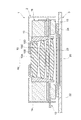
図1は、本発明の実施形態を説明するための撮像モジュールの一例の外観を示し、図2は、図1の撮像モジュールの断面を示す。
図1は、本発明の実施形態を説明するための撮像モジュールの一例の外観を示し、図2は、図1の撮像モジュールの断面を示す。
撮像モジュール1は、レンズユニット2と、レンズユニット2が固定される撮像素子ユニット3とを備える。
レンズユニット2は、レンズ群10と、レンズ駆動装置11と、フレキシブル基板12とを有する。
レンズ群10は、筒状のレンズバレル13に収容され、レンズバレル13によって一体に支持されている。なお、レンズ群10は、図示の例ではレンズ10A,10B,10C,10Dの4枚のレンズによって構成されているが、レンズの枚数は4枚に限られない。
レンズ駆動装置11は、レンズ群10を支持するレンズバレル13をレンズ光軸Az沿って移動させるフォーカス調整を行う。また、レンズ駆動装置11は、レンズバレル13を、レンズ光軸Azに垂直な面に沿って移動させる像振れ補正を行う。なお、レンズバレル13を、レンズ光軸Azに垂直な面に対して傾動させることによって像振れ補正を行うように構成してもよい。また、レンズ群10のうち一部のレンズを移動させることによってフォーカス調整や像振れ補正を行うように構成してもよい。
レンズ群10及びレンズバレル13並びにレンズ駆動装置11は筐体14に収容されており、レンズバレル13と筐体14との間で筐体14の底部に開いた開口は底部ブロック15によって塞がれている。
フレキシブル基板12は、レンズ駆動装置11を動作させるための信号(電力を含む)
を伝送する配線群を含んで構成されている。
を伝送する配線群を含んで構成されている。
撮像素子ユニット3は、撮像素子20と、外部接続部21が設けられた回路とを有する。
撮像素子20は、CCD(Charge Coupled Device)イメージセンサやCMOS(Complementary Metal-Oxide Semiconductor)イメージセンサなどの撮像素子であり、例えば300万~1000万画素の比較的高画素数の撮像素子である。
撮像素子20は、素子固定基板22に実装されており、カバーガラス23によって覆われている。カバーガラス23は、カバーホルダ24に支持されて素子固定基板22に配置されている。
撮像素子ユニット3に設けられる回路は、撮像素子20及びレンズユニット2のレンズ駆動装置11を動作させるための回路であり、素子固定基板22及び素子固定基板22から延設されたフレキシブル基板25に設けられている。外部接続部21は、撮像素子ユニット3の回路を外部機器の回路に接続するためのものであって、図示の例では、フレキシブル基板25の先端部に設けられている。そして、このフレキシブル基板25には、レンズユニット2のフレキシブル基板12が接続される接続部26が設けられている。レンズユニット2のレンズ駆動装置11は、フレキシブル基板12に含まれる配線群を介して、撮像素子ユニット3の回路に接続されている。
レンズユニット2は、レンズ群10の結像面を撮像素子20の受像面に一致させた状態で撮像素子ユニット3に組み付けられ、その状態で固定される。レンズユニット2と撮像素子ユニット3との固定は、例えばレンズユニット2の筐体14又は底部ブロック15と、撮像素子ユニット3の素子固定基板22又はカバーホルダ24とを接着することによって行われる。
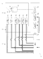
図3は、撮像モジュール1の機能ブロックを示す。
レンズユニット2のレンズ駆動装置11は、レンズバレル13をレンズ光軸Azに沿って移動させるアクチュエータ30zと、レンズ光軸Azに垂直な面内における直交2軸Ax,Ayのうちレンズバレル13をAx軸方向に沿って移動させるアクチュエータ30xと、レンズバレル13をAy軸方向に沿って移動させるアクチュエータ30yとを有する。
また、レンズ駆動装置11は、レンズバレル13のAx軸方向の位置を検出する位置センサ31xと、レンズバレル13のAy軸方向の位置を検出する位置センサ31yと、レンズバレル13のAz軸方向の位置を検出する位置センサ31zとを有する。
撮像素子ユニット3の回路には、撮像モジュール1に作用するAx軸回りの角速度を検出する角速度センサ32xと、撮像モジュール1に作用するAy軸回りの角速度を検出する角速度センサ32yと、アクチュエータ30x,30y,30zを駆動する制御IC(Integrated Circuit)34とが設けられている。
制御IC34は、位置センサ31zから出力される位置信号及び撮像素子20から出力される画像信号に基づき、フォーカス調整のためのレンズバレル13のAz軸方向の移動量を算出する。また、制御IC34は、角速度センサ32x,32yから出力される角速度信号及び位置センサ31x,31yから出力される位置信号に基づき、像振れ補正のためのレンズバレル13のAx軸方向及びAy軸方向の移動量を算出する。制御IC34じは、算出した各方向への移動量に基づいて、アクチュエータ30x,30y,30zを制御する。
角速度センサ32x,32y及び制御IC34の動作電力は、撮像素子ユニット3の外部接続部21に接続される外部機器から供給される。また、アクチュエータ30x,30y,30z及び位置センサ31x,31y,31zの動作電力は制御IC34から供給される。
以上の構成において、位置センサ31x,31y,31zから出力される位置信号を制御IC34に伝送する配線、並びに制御IC34から出力されるアクチュエータ30x,30y,30z及び位置センサ31x,31y,31zの動作電力をアクチュエータ30x,30y,30z及び位置センサ31x,31y,31zの各々に伝送する配線は、フレキシブル基板12によって配線されている。なお、図3において、動作電力を伝送する配線は太い実線で、位置信号を伝送する配線は細い実線で示している。
アクチュエータ30x,30y,30zとして、図示の例ではボイスコイルモータ(VCM)が用いられており、一つのVCMにつき典型的には2本の配線を要する。また、位置センサ31x,31y,31zとして、図示の例ではホール素子が用いられており、一つのホール素子につき典型的には4本の配線を要する。したがって、フレキシブル基板12には多数の配線が含まれることとなる。
なお、図示の例では、角速度センサ32x,32y、制御IC34が、いずれも撮像素子ユニット3に設けられているが、例えば制御IC34をレンズユニット2に設けてもよく、その場合には、制御IC34からアクチュエータ30x,30y,30zや位置センサ31x,31y,31zの各々に動作電力を伝送する配線に替えて、制御IC34の動作電力を伝送する配線や、撮像素子20から出力される画像信号及び角速度センサ32x,32yから出力される角速度信号を制御IC34に伝送する配線がフレキシブル基板12に含まれることとなる。
フレキシブル基板12に含まれる配線群は、その配線経路の少なくとも一部において複数の配線組に分けられ、配線組毎にフレキシブルに構成されたフレキシブル配線部分が設けられる。
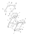
図4は、フレキシブル基板12の平面図を示す。
フレキシブル基板12は、レンズユニット2の筐体14内に収容される収容領域A1と、筐体14の外に導出される導出領域A2とを有する。
収容領域A1にはレンズバレル13を挿通させる円形孔40が形成されている。収容領域A1は、レンズバレル13の外周を取り囲んで配置され、同じくレンズバレル13の外周に配置されているレンズ駆動装置11に接続される。そして、収容領域A1には、円形孔40に連なるスリット41が形成されており、スリット41によって分離され、互いに並行する二つの部分基板12a-1,12a-2が設けられている。
導出領域A2は、レンズユニット2の筐体14から撮像素子ユニット3の外部接続部21を臨むAy軸方向に向けられた筐体14の側面から外部接続部21に向けて導出され、撮像素子ユニット3の接続部26に接続される(図1参照)。
部分基板12a-1,12a-2は、フレキシブル基板12によって配線される配線群Wを二組に振り分けることにより構成される配線組W1,W2をそれぞれ含み、配線組W1,W2毎に設けられる上記のフレキシブル配線部分を構成している。フレキシブル配線部分12a-1,12a-2は、導出領域A2の導出方向(Ay軸方向)に互いに並行して延在している。また、フレキシブル配線部分12a-1は、レンズ光軸Az及びAy軸を面上に沿って含む面である中心面CによってAx軸方向に分割された2つの領域の一方に設けられている。またフレキシブル配線部分12a-2は、中心面CによってAx軸方向に分割された2つの領域の他方に設けられている。したがって、フレキシブル配線部分12a-1,12a-2は、中心面Cを挟んで両側に設けられている。より具体的には、フレキシブル配線部分12a-1,12a-2は、中心面Cを挟んで対称に設けられている。フレキシブル配線部分12a-1,12a-2を分離しているスリット41は、例えば切れ込みであってもよいが、図示の例では、矩形孔として形成されており、フレキシブル配線部分12a-1,12a-2の間には空間があけられている。すなわち、フレキシブル配線部分12a-1,12a-2は、互いに空間を介して配置される。
なお、配線群Wを複数の配線組に振り分ける際の分け方は任意であり、例えば位置センサ31x,31y,31zの各々に動作電力を伝送する配線、及び位置センサ31x,31y,31zから制御IC34に位置信号を伝送する配線を一組とし、アクチュエータ30x,30y,30zの各々に動作電力を伝送する配線を一組としてもよいし。あるいは、位置センサ31x,31y,31z及びアクチュエータ30x,30y,30zの各々に動作電力を伝送する配線を一組とし、位置センサ31x,31y,31zから制御IC34に位置信号を伝送する配線を一組としてもよい。また、配線組の組数も、二組に限られず、三組以上としてもよい。
<撮像モジュールの製造方法>
図5は、撮像モジュール1の製造方法の概略を示す。
図5は、撮像モジュール1の製造方法の概略を示す。
撮像モジュール1は、レンズユニット2と撮像素子ユニット3との相対位置及び相対位置姿勢が調整され、調整後にレンズユニット2と撮像素子ユニット3とが固定されることにより製造される。
レンズユニット2と撮像素子ユニット3との相対位置及び相対姿勢の調整には、測定チャート50が用いられる。測定チャート50の表面には複数のチャート画像CH1,CH2,CH3,CH4,CH5が印刷されている。チャート画像CH1,CH2,CH3,CH4,CH5は、黒色線が一定間隔で配列された、いわゆるラダー状のチャートパターンであって、同一の画像とされている。
レンズユニット2は、レンズ光軸Azが測定チャート50の中心を通り測定チャート50に直交するZ軸に一致した状態に保持されている。さらに、図示の例では、レンズユニット2は、フレキシブル配線部分12a-1,12a-2の延在方向(Ay軸方向)がZ軸に直交する2軸(X軸,Y軸)のうちの一軸方向(図示の例ではY軸方向)に平行な状態に保持されている。
撮像素子ユニット3は、保持部材51によって、撮像素子20の受像面の中心位置がZ軸上に配置された状態に保持されている。保持部材51は、Z軸方向に移動可能に構成されており、また、撮像素子20の受像面の中心位置を回転中心にしてX軸回り及びY軸回りに回転可能に構成されている。したがって、撮像素子20の受像面の中心位置とZ軸との位置関係は、撮像素子ユニット3の回転にかかわらず一定に保たれる。
撮像素子ユニット3の外部接続部21には、コネクタケーブル52が接続される。コネクタケーブル52は、撮像素子ユニット3の撮像素子20を動作させるための信号及び撮像素子ユニット3から出力される画像信号を伝送する配線を含む。また、コネクタケーブル52は、レンズユニット2のレンズ駆動装置11を動作させるための信号を伝送する配線を含む。
図6は、撮像モジュール1の製造工程のフローを示す。
まず、撮像素子ユニット3のZ軸上に離散的に設定された複数の測定位置に撮像素子ユニット3を移動させ、各測定位置にて測定チャート50を撮像し、複数の画像を取得する(ステップS1)。
次いで、取得された複数の画像から、レンズユニット2のレンズ群10の近似結像面を算出する(ステップS2)。近似結像面の算出は、特開2010-21985号公報に記載された方法を用いることができ、撮像素子ユニット3の撮像素子20の受像面において測定チャート50のチャート画像CH1,CH2,CH3,CH4,CH5の各々の像が形成される画素領域毎に、各測定位置での合焦度合いを評価する。合焦度合いの評価には、例えばコントラスト伝達関数(CTF:Contrast Transfer Function)を用いることができ、各画素領域に対応する画像領域のCTF値が高いほどに、合焦度合いが高いものとみなすことができる。そして、画素領域毎に、複数の画像から得られる複数の合焦度合いに基づいて、合焦度合いが最大となるZ軸上の座標値を合焦座標値として算出する。そして、撮像素子20の受像面をXY座標平面に投影したときの各画素領域のXY座標値と、その画素領域の合焦座標値(Z軸上の座標値)との組み合わせで表されるXYZ座標系の点群から近似平面を算出し、この近似平面を近似結像面とする。
次いで、近似結像面とZ軸との交点である結像面座標値Fと、XY座標平面に対する近似結像面のX軸回りの傾き角θX及びY軸回りの傾き角θYとを算出し(ステップS3)、算出された結像面座標値F及び傾き角θX,θYに基づいて、撮像素子ユニット3をZ軸方向に移動させ、またX軸回り及びY軸回りに回転させて、撮像素子20の受像面を近似結像面に一致させる(ステップS4)。
そして、相対位置及び相対姿勢が調整されたレンズユニット2と撮像素子ユニット3とを固定する(ステップS5)。
なお、本例では撮像素子ユニット3を移動させて複数の画像を取得しているが、測定チャート50又はレンズユニット2のZ軸上における位置に関して複数の測定位置を設定し、測定チャート50又はレンズユニット2を各測定位置に移動させて複数の画像を取得するようにしてもよい。
以上の工程において、近似結像面を算出するための複数の画像を取得する際に、レンズユニット2のレンズ駆動装置11を動作させるための信号を、コネクタケーブル52を介して撮像素子ユニット3の外部接続部21に入力し、レンズユニット2のレンズバレル13を所定の位置に配置する。レンズバレル13の位置として、Az軸方向の位置についてはフォーカスのNEAR端に対応する位置を例示することができ、Ax軸方向及びAy軸方向の位置については原点位置を例示することができる。
コネクタケーブル52を介して撮像素子ユニット3の外部接続部21に入力される信号であってレンズユニット2のレンズ駆動装置11を動作させるための信号としては、レンズバレル13の位置を撮像素子ユニット3の制御IC34に対して指示する制御信号及び撮像素子ユニット3の制御IC34の動作電力が含まれる。制御IC34は、外部接続部21に入力された上記制御信号、及び位置センサ31x,31y,31zから出力される位置信号に基づいてレンズバレル13の各方向の移動量を算出し、算出した各方向への移動量に基づいてアクチュエータ30x,30y,30zを制御する。
そして、位置センサ31x,31y,31zから出力される位置信号、並びに、制御IC34から出力されるアクチュエータ30x,30y,30z及び位置センサ31x,31y,31zの動作電力は、フレキシブル基板12に含まれる配線群によって、レンズユニット2と撮像素子ユニット3との間で伝送される。
レンズ駆動装置11を動作させてレンズバレル13を所定の位置に配置した状態で近似結像面を算出するための複数の画像を取得することにより、撮像素子20の受像面における上記画素領域毎の合焦度合いを適正に評価することが可能となる。それにより、近似結像面を精度よく算出することができ、レンズユニット2と撮像素子ユニット3との相対位置姿勢の調整の精度を高めることができる。なお、レンズ駆動装置11のアクチュエータ30x,30y,30zのみを動作させてレンズバレル13の位置を開ループ制御するようにしてもよいが、位置センサ31x,31y,31zを併せて動作させてレンズバレル13の位置を閉ループ制御することにより、レンズバレル13を所定の位置に精度よく配置することができる。
図5を参照して、本撮像モジュール1では、フレキシブル基板12に含まれる配線群Wが二組の配線組W1,W2に振り分けられ、配線組W1,W2毎にフレキシブル配線部分12a-1,12a-2が設けられている。撮像素子ユニット3をX軸回り及びY軸回りに回転させて撮像素子20の受像面を近似結像面に一致させる際に、フレキシブル基板12は、その剛性に起因して、捻りや曲げに伴う反力をレンズユニット2及び撮像素子ユニット3に作用させるが、互いに分離されたフレキシブル配線部分12a-1,12a-2においてフレキシブル基板12の剛性を小さくできる。それにより、フレキシブル基板12の反力を軽減することができる。特に、本撮像モジュール1では、フレキシブル配線部分12a-1,12a-2の間に空間があけられており、フレキシブル基板12の反力を一層軽減することができる。
そして、撮像素子20の受像面を近似結像面に一致させる際の撮像素子ユニット3のX軸回り及びY軸回りの回転は典型的には±0.05°以内の極僅かな回転であり、フレキシブル基板12の反力が軽減されることによって、レンズユニット2と撮像素子ユニット3との相対位置及び相対姿勢の調整の精度を高め、且つ、調整に要する時間も短縮することができる。
さらに、本撮像モジュール1では、フレキシブル配線部分12a-1,12a-2が、レンズ光軸Azを面上に沿って含みフレキシブル配線部分12a-1,12a-2の延在方向(Ay軸方向)に平行な中心面Cを挟んで両側に設けられている。そして、撮像素子ユニット3の一方の回転軸であるY軸が中心面Cの面内に配置されている。そのため、フレキシブル配線部分12a-1,12a-2の捻りや曲げに伴う反力は、Y軸を挟んで略均等に配分されてレンズユニット2及び撮像素子ユニット3に作用する。それにより、レンズユニット2と撮像素子ユニット3との相対位置及び相対姿勢の調整が容易となる。反力を略均等に配分する観点から、フレキシブル配線部分12a-1,12a-2が中心面Cを挟んで対称に設けられていることも好ましい。
フレキシブル基板12の反力を軽減することは、撮像素子ユニット3の撮像素子20の画素ピッチが小さくなる程に有用となり、画素ピッチが1μm以下である場合に特に有用である。画素ピッチが小さくなる、つまりは画素サイズが小さくなると、許容錯乱円が小さくなり、一画素あたりに入る光が減るため、開放F値が小さい明るいレンズが用いられる。そして、F値が小さくなると焦点深度が浅くなるので、レンズユニット2と撮像素子ユニット3との相対位置及び相対姿勢の厳密な調整が必要とされ、画素ピッチが1μm以下となると、厳密な調整の必要性が特に顕著になる。なお、画素ピッチとは、撮像素子20が有する画素に含まれる光電変換領域の中心間距離のうち、最も小さい距離のことをいう。
図7は、撮像モジュール1の製造方法の他の例の概略を示す。
図7に示す例では、レンズユニット2と撮像素子ユニット3との相対位置姿勢が調整される際に、フレキシブル基板12にコネクタケーブル53が接続され、レンズ駆動装置11を動作させるための信号がコネクタケーブル53を介してレンズユニット2に直接入力される。フレキシブル基板12は、レンズユニット2と撮像素子ユニット3との相対位置姿勢の調整及び固定が済んだ後、撮像素子ユニット3の接続部26に接続される。
レンズ駆動装置11を動作させるための信号をレンズユニット2に直接入力する方法としては、例えばレンズユニット2の筐体14の側面に端子群を設け、端子群にプローブを接触させて信号を入力することも考えられるが、プローブの接触に伴って、レンズユニット2の変形や位置ずれが懸念される。これに対して、本例ではフレキシブル基板12が介在することにより、レンズユニット2の変形や位置ずれが抑制される。また、撮像モジュール1では、互いに分離されたフレキシブル配線部分12a-1,12a-2においてフレキシブル基板12の剛性を小さくできるので、フレキシブル基板12を介して外力が伝わることを防ぐことができる。
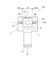
次に、撮像モジュールの他の例を説明する。
上述した撮像モジュール1では、フレキシブル基板12によって配線される配線群Wを二組に振り分けることにより構成される配線組W1,W2毎のフレキシブル配線部分12a-1,12a-2がレンズユニット2の筐体14内に設けられているが、以下に説明する例では、配線組W1,W2毎のフレキシブル配線部分が筐体14の外に設けられている。配線組W1,W2毎のフレキシブル配線部分を筐体14の外に設けることによって、フレキシブル配線部分を延長することができ、フレキシブル基板12の捻りや曲げに伴う反力を一層軽減することができる。また、配線組W1,W2毎のフレキシブル配線部分を筐体14の外に設けることによって、配線組W1,W2の配線経路の自由度も高まる。
図8に示す撮像モジュール101において、レンズユニット2のレンズ駆動装置11と撮像素子ユニット3の回路とを接続するフレキシブル基板112は、レンズユニット2の筐体14内に収容される収容領域A1と、筐体14の外に導出される導出領域A2-1,A2-2とを有している。
導出領域A2-1は一方の配線組W1を含み、配線組W1のフレキシブル配線部分を構成している。また、導出領域A2-2は他方の配線組W2を含み、配線組W2のフレキシブル配線部分を構成している。導出領域A2-1,A2-2は、筐体14から撮像素子ユニット3の外部接続部21を臨むAy軸方向と直交するAx軸方向に向けられた筐体14の一対の側面からそれぞれ導出され、互いに反対方向に導出されている。
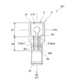
図9に示す撮像モジュール201において、レンズユニット2のレンズ駆動装置11と撮像素子ユニット3の回路とを接続するフレキシブル基板212は、レンズユニット2の筐体14内に収容される収容領域A1と、筐体14の外に導出される導出領域A2とを有している。
導出領域A2には、収容領域A1から延びるスリット241が形成されており、スリット241によって分離され、互いに並行する二つの部分基板212a-1,212a-2が設けられている。部分基板212a-1,212a-2は、配線組W1,W2をそれぞれ含み、配線組W1,W2毎に設けられるフレキシブル配線部分をそれぞれ構成している。フレキシブル配線部分212a-1,212a-2は、筐体14から撮像素子ユニット3の外部接続部21を臨むAy軸方向と直交するAx軸方向に向けられた筐体14の一側面から導出され、同一方向に導出されている。そして、フレキシブル配線部分212a-1,212a-2は互いに並行して延在する。また、フレキシブル配線部分212a-1,212a-2は、レンズ光軸Azを面上に沿って含みフレキシブル配線部分212a-1,212a-2の延在方向に平行な中心面Cを挟んで両側に設けられており、中心面Cを挟んで対称に設けられている。
このように、フレキシブル配線部分212a-1,212a-2を同一方向に筐体14から導出するようにすれば、配線部分を互いに異なる方向に導出する場合(図8参照)に比べて、撮像モジュールを小型化することができる。
図10に示す撮像モジュール301において、レンズユニット2のレンズ駆動装置11と撮像素子ユニット3の回路とを接続するフレキシブル基板312は、レンズユニット2の筐体14内に収容される収容領域A1と、筐体14の外に導出される導出領域A2とを有している。
導出領域A2には、収容領域A1から延びるスリット341が形成されており、スリット341によって分離され、互いに並行する二つの部分基板312a-1,312a-2が設けられている。部分基板312a-1,312a-2は、配線組W1,W2をそれぞれ含み、配線組W1,W2毎に設けられるフレキシブル配線部分をそれぞれ構成している。フレキシブル配線部分312a-1,312a-2は、筐体14から撮像素子ユニット3の外部接続部21を臨むAy軸方向に向けられた筐体14の一側面から導出され、同一方向に導出されている。そして、フレキシブル配線部分312a-1,312a-2は互いに並行して延在する。また、フレキシブル配線部分312a-1,312a-2は、レンズ光軸Azを面上に沿って含みフレキシブル配線部分312a-1,312a-2の延在方向に平行な中心面Cを挟んで両側に設けられており、中心面Cを挟んで対称に設けられている。
このように、フレキシブル配線部分312a-1,312a-2を、撮像素子ユニット3の外部接続部21に向けて筐体14から導出するようにすれば、筐体14から外部接続部21を臨む方向とは異なる方向に導出する場合(図9参照)に比べて、撮像モジュールを小型化することができる。また、本例ではフレキシブル配線部分312a-1,312a-2が導出領域A2の全長に亘って設けられており、フレキシブル基板312の捻りや曲げに伴う反力が一層軽減される。
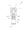
上述した撮像モジュール1,101,201,301では、レンズユニット2のレンズ駆動装置11と撮像素子ユニット3の回路とを接続する配線群が一つのフレキシブル基板によって配線され、配線組W1,W2毎のフレキシブル配線部分はフレキシブル基板の一部によってそれぞれ構成されている。これに対して、図11に示す撮像モジュール401では、配線組W1はフレキシブル基板412-1によって配線され、配線組W2はフレキシブル基板412-2によって配線されている。このように、配線組毎に異なるフレキシブル基板を用いて、配線組毎のフレキシブル配線部分を設けるようにしてもよい。この場合に、複数のフレキシブル基板(フレキシブル配線部分)を、レンズユニット2の筐体14から互いに異なる方向に導出してもよいが、複数のフレキシブル基板を同一方向に導出し、さらに撮像素子ユニット3の外部接続部21に向けて導出するようにすれば、撮像素子モジュールを小型化することができる。
なお、上述した撮像モジュール1,101,201,301,401において、レンズユニット2と撮像素子ユニット3の相対位置姿勢の調整及び両ユニット2,3の固定が済んだ後に、フレキシブル配線部分の各々の少なくとも一部を撮像素子ユニット3に固定してもよい。それにより、フレキシブル配線部分のばたつきなどが防止され、撮像モジュールの取り扱いが容易となり、フレキシブル配線部分がレンズユニット2の筐体14の外に設けられる場合に特に有用である。
以上説明した撮像モジュールは、図示しない基板等の支持部材に支持され、デジタルカメラや車載用カメラ等の電子機器の筐体内に配置され、撮像装置として供される。撮像モジュールの組み込み対象としては、上記の他、例えば、PC(Personal Computer)内蔵型又は外付け型のPC用カメラ、カメラ付きインターフォン、或いは、撮影機能を有する携帯端末装置、腕時計型端末装置、眼鏡型端末装置等の電子機器を挙げることができる。携帯端末装置としては、例えば、携帯電話機やスマートフォン、PDA(Personal Digital Assistants)、携帯型ゲーム機等が挙げられる。
本発明は上述した実施形態に限定されるものではなく、実施形態の各構成を相互に組み合わせることや、明細書の記載、並びに周知の技術に基づいて、当業者が変更、応用することも本発明の予定するところであり、保護を求める範囲に含まれる。
以上説明したとおり、本明細書には下記の事項が開示されている。
(1) 撮像素子及び外部接続部が設けられた回路を有する撮像素子ユニットと、レンズ群と、このレンズ群の少なくとも一部のレンズを上記撮像素子に対して移動させてフォーカス調整及び像振れ補正を行うレンズ駆動装置と、を有し、上記撮像素子ユニットに固定されたレンズユニットと、上記レンズ駆動装置を上記回路に接続する配線群と、を備え、上記配線群は、配線経路の少なくとも一部において複数の配線組に分かれており、上記配線組毎に設けられ、且つ互いに分離された複数のフレキシブル配線部分をさらに備える撮像モジュール。
(2) 上記(1)の撮像モジュールであって、上記撮像素子の画素ピッチは1μm以下である撮像モジュール。
(3) 上記(1)又は(2)の撮像モジュールであって、上記レンズユニットは、上記レンズ駆動装置を収容する筐体をさらに有し、上記複数のフレキシブル配線部分の各々の少なくとも一部は、上記筐体の外部に設けられている撮像モジュール。
(4) 上記(3)の撮像モジュールであって、上記複数の配線組の各々は、同一方向に上記筐体から導出されている撮像モジュール。
(5) 上記(4)の撮像モジュールであって、上記複数の配線組の各々は、上記外部接続部に向けて上記筐体から導出されている撮像モジュール。
(6) 上記(1)から(5)のいずれか一つの撮像モジュールであって、上記レンズ駆動装置は、移動される上記レンズの位置を検出するセンサを含み、上記配線群は、上記センサから出力される位置信号を伝送する配線を含む撮像モジュール。
(7) 上記(1)から(6)のいずれか一つの撮像モジュールであって、上記複数のフレキシブル配線部分は、互いに並行して延在し、且つ上記レンズ群の光軸を面上に沿って含みこれらの複数のフレキシブル配線部分の延在方向と平行な中心面を挟んで両側に設けられている撮像モジュール。
(8) 上記(7)の撮像モジュールであって、上記複数のフレキシブル配線部分は、互いに空間を介して配置される撮像モジュール。
(9) 上記(1)から(8)のいずれか一つの撮像モジュールであって、上記複数のフレキシブル配線部分は、互いに並行して延在し、且つ上記レンズ群の光軸を面上に沿って含みこれらの複数のフレキシブル配線部分の延在方向と平行な中心面を挟んで対称に設けられている撮像モジュール。
(10) 上記(1)から(9)のいずれか一つの撮像モジュールであって、上記複数のフレキシブル配線部分の各々の少なくとも一部は、上記撮像素子ユニットに固定されている撮像モジュール。
(11) 上記(1)から(10)のいずれか一つの撮像モジュールを搭載した電子機器。
(12) 上記(1)から(10)のいずれか一つの撮像モジュールの製造方法であって、測定チャートに直交するZ軸上にセットされた上記レンズユニット及び上記撮像素子ユニット、並びにこの測定チャートのいずれかを複数の測定位置に移動させ、上記複数の測定位置の各々において、上記外部接続部を通じて上記レンズ駆動装置を動作させた状態で、上記レンズユニットによって結像される測定チャート像を上記撮像素子により撮像することにより複数の画像を取得し、取得された上記複数の画像に基づいて、Z軸上での上記レンズユニットと上記撮像素子ユニットとの相対位置及びZ軸に直交するX軸及びY軸回りの上記レンズユニットと上記撮像素子ユニットとの相対姿勢の調整量を求め、求めた上記調整量に基づいて上記レンズユニットと上記撮像素子ユニットとの上記相対位置及び上記相対姿勢を調整し、上記相対位置及び上記相対姿勢が調整された上記レンズユニットと上記撮像素子ユニットとを固定する撮像モジュールの製造方法。
(13) 上記(1)から(10)のいずれか一つの撮像モジュールの製造方法であって、測定チャートに直交するZ軸上にセットされた上記レンズユニット及び上記撮像素子ユニット、並びにこの測定チャートのいずれかを複数の測定位置に移動させ、上記複数の測定位置の各々において、上記配線群を通じて上記レンズ駆動装置を動作させた状態で、上記レンズユニットによって結像される測定チャート像を上記撮像素子により撮像することにより複数の画像を取得し、取得された上記複数の画像に基づいて、Z軸上での上記レンズユニットと上記撮像素子ユニットとの相対位置及びZ軸に直交するX軸及びY軸回りの上記レンズユニットと上記撮像素子ユニットとの相対姿勢の調整量を求め、求めた上記調整量に基づいて上記レンズユニットと上記撮像素子ユニットとの上記相対位置及び上記相対姿勢を調整し、上記相対位置及び上記相対姿勢が調整された上記レンズユニットと上記撮像素子ユニットとを固定し、上記配線群を上記撮像素子ユニットの上記回路に接続する撮像モジュールの製造方法。
(14) 上記(12)又は(13)の撮像モジュールの製造方法であって、上記複数のフレキシブル配線部分は、互いに並行して延在し、且つ上記レンズ群の光軸を面上に沿って含みこれらの複数のフレキシブル配線部分の延在方向と平行な中心面を挟んで両側に設けられており、X軸方向及びY軸方向のいずれか一方は、上記中心面の面内方向である撮像モジュールの製造方法。
(15) 上記(12)から(14)のいずれか一つの撮像モジュールの製造方法であって、上記複数のフレキシブル配線部分は、互いに並行して延在し、且つ上記レンズ群の光軸を面上に沿って含みこれらの複数のフレキシブル配線部分の延在方向と平行な中心面を挟んで対称に設けられており、X軸方向及びY軸方向のいずれか一方は、上記中心面の面内方向である撮像モジュールの製造方法。
(16) 上記(12)から(15)のいずれか一つの撮像モジュールの製造方法であって、上記レンズユニットと上記撮像素子ユニットとを固定した後に、上記複数のフレキシブル配線部分の各々の少なくとも一部を上記撮像素子ユニットに固定する撮像モジュールの製造方法。
(2) 上記(1)の撮像モジュールであって、上記撮像素子の画素ピッチは1μm以下である撮像モジュール。
(3) 上記(1)又は(2)の撮像モジュールであって、上記レンズユニットは、上記レンズ駆動装置を収容する筐体をさらに有し、上記複数のフレキシブル配線部分の各々の少なくとも一部は、上記筐体の外部に設けられている撮像モジュール。
(4) 上記(3)の撮像モジュールであって、上記複数の配線組の各々は、同一方向に上記筐体から導出されている撮像モジュール。
(5) 上記(4)の撮像モジュールであって、上記複数の配線組の各々は、上記外部接続部に向けて上記筐体から導出されている撮像モジュール。
(6) 上記(1)から(5)のいずれか一つの撮像モジュールであって、上記レンズ駆動装置は、移動される上記レンズの位置を検出するセンサを含み、上記配線群は、上記センサから出力される位置信号を伝送する配線を含む撮像モジュール。
(7) 上記(1)から(6)のいずれか一つの撮像モジュールであって、上記複数のフレキシブル配線部分は、互いに並行して延在し、且つ上記レンズ群の光軸を面上に沿って含みこれらの複数のフレキシブル配線部分の延在方向と平行な中心面を挟んで両側に設けられている撮像モジュール。
(8) 上記(7)の撮像モジュールであって、上記複数のフレキシブル配線部分は、互いに空間を介して配置される撮像モジュール。
(9) 上記(1)から(8)のいずれか一つの撮像モジュールであって、上記複数のフレキシブル配線部分は、互いに並行して延在し、且つ上記レンズ群の光軸を面上に沿って含みこれらの複数のフレキシブル配線部分の延在方向と平行な中心面を挟んで対称に設けられている撮像モジュール。
(10) 上記(1)から(9)のいずれか一つの撮像モジュールであって、上記複数のフレキシブル配線部分の各々の少なくとも一部は、上記撮像素子ユニットに固定されている撮像モジュール。
(11) 上記(1)から(10)のいずれか一つの撮像モジュールを搭載した電子機器。
(12) 上記(1)から(10)のいずれか一つの撮像モジュールの製造方法であって、測定チャートに直交するZ軸上にセットされた上記レンズユニット及び上記撮像素子ユニット、並びにこの測定チャートのいずれかを複数の測定位置に移動させ、上記複数の測定位置の各々において、上記外部接続部を通じて上記レンズ駆動装置を動作させた状態で、上記レンズユニットによって結像される測定チャート像を上記撮像素子により撮像することにより複数の画像を取得し、取得された上記複数の画像に基づいて、Z軸上での上記レンズユニットと上記撮像素子ユニットとの相対位置及びZ軸に直交するX軸及びY軸回りの上記レンズユニットと上記撮像素子ユニットとの相対姿勢の調整量を求め、求めた上記調整量に基づいて上記レンズユニットと上記撮像素子ユニットとの上記相対位置及び上記相対姿勢を調整し、上記相対位置及び上記相対姿勢が調整された上記レンズユニットと上記撮像素子ユニットとを固定する撮像モジュールの製造方法。
(13) 上記(1)から(10)のいずれか一つの撮像モジュールの製造方法であって、測定チャートに直交するZ軸上にセットされた上記レンズユニット及び上記撮像素子ユニット、並びにこの測定チャートのいずれかを複数の測定位置に移動させ、上記複数の測定位置の各々において、上記配線群を通じて上記レンズ駆動装置を動作させた状態で、上記レンズユニットによって結像される測定チャート像を上記撮像素子により撮像することにより複数の画像を取得し、取得された上記複数の画像に基づいて、Z軸上での上記レンズユニットと上記撮像素子ユニットとの相対位置及びZ軸に直交するX軸及びY軸回りの上記レンズユニットと上記撮像素子ユニットとの相対姿勢の調整量を求め、求めた上記調整量に基づいて上記レンズユニットと上記撮像素子ユニットとの上記相対位置及び上記相対姿勢を調整し、上記相対位置及び上記相対姿勢が調整された上記レンズユニットと上記撮像素子ユニットとを固定し、上記配線群を上記撮像素子ユニットの上記回路に接続する撮像モジュールの製造方法。
(14) 上記(12)又は(13)の撮像モジュールの製造方法であって、上記複数のフレキシブル配線部分は、互いに並行して延在し、且つ上記レンズ群の光軸を面上に沿って含みこれらの複数のフレキシブル配線部分の延在方向と平行な中心面を挟んで両側に設けられており、X軸方向及びY軸方向のいずれか一方は、上記中心面の面内方向である撮像モジュールの製造方法。
(15) 上記(12)から(14)のいずれか一つの撮像モジュールの製造方法であって、上記複数のフレキシブル配線部分は、互いに並行して延在し、且つ上記レンズ群の光軸を面上に沿って含みこれらの複数のフレキシブル配線部分の延在方向と平行な中心面を挟んで対称に設けられており、X軸方向及びY軸方向のいずれか一方は、上記中心面の面内方向である撮像モジュールの製造方法。
(16) 上記(12)から(15)のいずれか一つの撮像モジュールの製造方法であって、上記レンズユニットと上記撮像素子ユニットとを固定した後に、上記複数のフレキシブル配線部分の各々の少なくとも一部を上記撮像素子ユニットに固定する撮像モジュールの製造方法。
1 撮像モジュール
2 レンズユニット
3 撮像素子ユニット
10 レンズ群
11 レンズ駆動装置
12 フレキシブル基板
12a-1,12a-2 フレキシブル配線部分
14 筐体
20 撮像素子
21 外部接続部
22 素子固定基板
30x,30y,30z アクチュエータ
31x,31y 位置センサ
32x,32y 角速度センサ
34 制御IC
50 測定チャート
51 保持部材
52 コネクタケーブル
W1,W2 配線組
2 レンズユニット
3 撮像素子ユニット
10 レンズ群
11 レンズ駆動装置
12 フレキシブル基板
12a-1,12a-2 フレキシブル配線部分
14 筐体
20 撮像素子
21 外部接続部
22 素子固定基板
30x,30y,30z アクチュエータ
31x,31y 位置センサ
32x,32y 角速度センサ
34 制御IC
50 測定チャート
51 保持部材
52 コネクタケーブル
W1,W2 配線組
Claims (16)
- 撮像素子及び外部接続部が設けられた回路を有する撮像素子ユニットと、
レンズ群と、該レンズ群の少なくとも一部のレンズを前記撮像素子に対して移動させてフォーカス調整及び像振れ補正を行うレンズ駆動装置と、を有し、前記撮像素子ユニットに固定されたレンズユニットと、
前記レンズ駆動装置を前記回路に接続する配線群と、
を備え、
前記配線群は、配線経路の少なくとも一部において複数の配線組に分かれており、
前記配線組毎に設けられ、且つ互いに分離された複数のフレキシブル配線部分をさらに備える撮像モジュール。
- 請求項1記載の撮像モジュールであって、
前記撮像素子の画素ピッチは1μm以下である撮像モジュール。
- 請求項1又は2記載の撮像モジュールであって、
前記レンズユニットは、前記レンズ駆動装置を収容する筐体をさらに有し、
前記複数のフレキシブル配線部分の各々の少なくとも一部は、前記筐体の外部に設けられている撮像モジュール。
- 請求項3記載の撮像モジュールであって、
前記複数の配線組の各々は、同一方向に前記筐体から導出されている撮像モジュール。
- 請求項4記載の撮像モジュールであって、
前記複数の配線組の各々は、前記外部接続部に向けて前記筐体から導出されている撮像モジュール。
- 請求項1から5のいずれか一項記載の撮像モジュールであって、
前記レンズ駆動装置は、移動される前記レンズの位置を検出するセンサを含み、
前記配線群は、前記センサから出力される位置信号を伝送する配線を含む撮像モジュール。
- 請求項1から6のいずれか一項記載の撮像モジュールであって、
前記複数のフレキシブル配線部分は、互いに並行して延在し、且つ前記レンズ群の光軸を面上に沿って含み該複数のフレキシブル配線部分の延在方向と平行な中心面を挟んで両側に設けられている撮像モジュール。
- 請求項7記載の撮像モジュールであって、
前記複数のフレキシブル配線部分は、互いに空間を介して配置される撮像モジュール。
- 請求項1から8のいずれか一項記載の撮像モジュールであって、
前記複数のフレキシブル配線部分は、互いに並行して延在し、且つ前記レンズ群の光軸を面上に沿って含み該複数のフレキシブル配線部分の延在方向と平行な中心面を挟んで対称に設けられている撮像モジュール。
- 請求項1から9のいずれか一項記載の撮像モジュールであって、
前記複数のフレキシブル配線部分の各々の少なくとも一部は、前記撮像素子ユニットに固定されている撮像モジュール。
- 請求項1から10のいずれか一項記載の撮像モジュールを搭載した電子機器。
- 請求項1から10のいずれか一項記載の撮像モジュールの製造方法であって、
測定チャートに直交するZ軸上にセットされた前記レンズユニット及び前記撮像素子ユニット、並びに該測定チャートのいずれかを複数の測定位置に移動させ、
前記複数の測定位置の各々において、前記外部接続部を通じて前記レンズ駆動装置を動作させた状態で、前記レンズユニットによって結像される測定チャート像を前記撮像素子により撮像することにより複数の画像を取得し、
取得された前記複数の画像に基づいて、Z軸上での前記レンズユニットと前記撮像素子ユニットとの相対位置及びZ軸に直交するX軸及びY軸回りの前記レンズユニットと前記撮像素子ユニットとの相対姿勢の調整量を求め、
求めた前記調整量に基づいて前記レンズユニットと前記撮像素子ユニットとの前記相対位置及び前記相対姿勢を調整し、
前記相対位置及び前記相対姿勢が調整された前記レンズユニットと前記撮像素子ユニットとを固定する撮像モジュールの製造方法。
- 請求項1から10のいずれか一項記載の撮像モジュールの製造方法であって、
測定チャートに直交するZ軸上にセットされた前記レンズユニット及び前記撮像素子ユニット、並びに該測定チャートのいずれかを複数の測定位置に移動させ、
前記複数の測定位置の各々において、前記配線群を通じて前記レンズ駆動装置を動作させた状態で、前記レンズユニットによって結像される測定チャート像を前記撮像素子により撮像することにより複数の画像を取得し、
取得された前記複数の画像に基づいて、Z軸上での前記レンズユニットと前記撮像素子ユニットとの相対位置及びZ軸に直交するX軸及びY軸回りの前記レンズユニットと前記撮像素子ユニットとの相対姿勢の調整量を求め、
求めた前記調整量に基づいて前記レンズユニットと前記撮像素子ユニットとの前記相対位置及び前記相対姿勢を調整し、
前記相対位置及び前記相対姿勢が調整された前記レンズユニットと前記撮像素子ユニットとを固定し、
前記配線群を前記撮像素子ユニットの前記回路に接続する撮像モジュールの製造方法。
- 請求項12又は13記載の撮像モジュールの製造方法であって、
前記複数のフレキシブル配線部分は、互いに並行して延在し、且つ前記レンズ群の光軸を面上に沿って含み該複数のフレキシブル配線部分の延在方向と平行な中心面を挟んで両側に設けられており、
X軸方向及びY軸方向のいずれか一方は、前記中心面の面内方向である撮像モジュールの製造方法。
- 請求項12から14のいずれか一項記載の撮像モジュールの製造方法であって、
前記複数のフレキシブル配線部分は、互いに並行して延在し、且つ前記レンズ群の光軸を面上に沿って含み該複数のフレキシブル配線部分の延在方向と平行な中心面を挟んで対称に設けられており、
X軸方向及びY軸方向のいずれか一方は、前記中心面の面内方向である撮像モジュールの製造方法。
- 請求項12から15のいずれか一項記載の撮像モジュールの製造方法であって、
前記レンズユニットと前記撮像素子ユニットとを固定した後に、前記複数のフレキシブル配線部分の各々の少なくとも一部を前記撮像素子ユニットに固定する撮像モジュールの製造方法。
Applications Claiming Priority (2)
| Application Number | Priority Date | Filing Date | Title |
|---|---|---|---|
| JP2013160621A JP2016176967A (ja) | 2013-08-01 | 2013-08-01 | 撮像モジュール及び電子機器並びに撮像モジュールの製造方法 |
| JP2013-160621 | 2013-08-01 |
Publications (1)
| Publication Number | Publication Date |
|---|---|
| WO2015016023A1 true WO2015016023A1 (ja) | 2015-02-05 |
Family
ID=52431563
Family Applications (1)
| Application Number | Title | Priority Date | Filing Date |
|---|---|---|---|
| PCT/JP2014/068251 Ceased WO2015016023A1 (ja) | 2013-08-01 | 2014-07-09 | 撮像モジュール及び電子機器並びに撮像モジュールの製造方法 |
Country Status (2)
| Country | Link |
|---|---|
| JP (1) | JP2016176967A (ja) |
| WO (1) | WO2015016023A1 (ja) |
Families Citing this family (1)
| Publication number | Priority date | Publication date | Assignee | Title |
|---|---|---|---|---|
| WO2022225372A1 (ko) | 2021-04-23 | 2022-10-27 | 삼성전자 주식회사 | 카메라 모듈 및 그를 포함하는 전자 장치 |
Citations (3)
| Publication number | Priority date | Publication date | Assignee | Title |
|---|---|---|---|---|
| JP2010021985A (ja) * | 2008-01-15 | 2010-01-28 | Fujifilm Corp | 撮像素子の位置調整方法、カメラモジュール製造方法及び装置、カメラモジュール |
| JP2013024938A (ja) * | 2011-07-15 | 2013-02-04 | Mitsumi Electric Co Ltd | レンズ駆動装置 |
| JP2013088525A (ja) * | 2011-10-14 | 2013-05-13 | Sharp Corp | カメラモジュールおよびカメラモジュールの製造方法 |
-
2013
- 2013-08-01 JP JP2013160621A patent/JP2016176967A/ja active Pending
-
2014
- 2014-07-09 WO PCT/JP2014/068251 patent/WO2015016023A1/ja not_active Ceased
Patent Citations (3)
| Publication number | Priority date | Publication date | Assignee | Title |
|---|---|---|---|---|
| JP2010021985A (ja) * | 2008-01-15 | 2010-01-28 | Fujifilm Corp | 撮像素子の位置調整方法、カメラモジュール製造方法及び装置、カメラモジュール |
| JP2013024938A (ja) * | 2011-07-15 | 2013-02-04 | Mitsumi Electric Co Ltd | レンズ駆動装置 |
| JP2013088525A (ja) * | 2011-10-14 | 2013-05-13 | Sharp Corp | カメラモジュールおよびカメラモジュールの製造方法 |
Also Published As
| Publication number | Publication date |
|---|---|
| JP2016176967A (ja) | 2016-10-06 |
Similar Documents
| Publication | Publication Date | Title |
|---|---|---|
| US9674443B2 (en) | Imaging module, electronic device, and imaging-module manufacturing method | |
| US10197887B2 (en) | Actuator, camera module, and camera mounted device | |
| US9699364B2 (en) | Imaging module and electronic apparatus | |
| KR102003043B1 (ko) | 연성 인쇄회로기판 및 이를 구비한 소형 카메라 장치 | |
| US9565347B2 (en) | Imaging module and electronic apparatus | |
| CN103529531B (zh) | 镜头驱动装置 | |
| KR20200041545A (ko) | 카메라 모듈 | |
| KR101886362B1 (ko) | 카메라 모듈용 액츄에이터 이동감지 소자와 그들을 포함하는 카메라 모듈용 유연성 회로기판 | |
| US9596409B2 (en) | Imaging module and electronic apparatus | |
| CN115668966B (zh) | 相机致动器以及包括该相机致动器的相机装置 | |
| JP2006166202A (ja) | 光学装置及びデジタルカメラ | |
| WO2015015986A1 (ja) | 撮像モジュール、及びこれを備えた電子機器、並びに撮像モジュールの製造方法 | |
| JP6206456B2 (ja) | カメラユニット、およびカメラ | |
| US9791659B2 (en) | Imaging module and electronic device | |
| JP2014157309A (ja) | ステレオカメラユニット | |
| CN105122130A (zh) | 相机模块 | |
| US9979868B2 (en) | Image pickup module manufacturing method, and image pickup module manufacturing device | |
| US9609196B2 (en) | Imaging module and electronic device | |
| CN117413525A (zh) | 相机致动器和包括该相机致动器的相机设备 | |
| WO2015016023A1 (ja) | 撮像モジュール及び電子機器並びに撮像モジュールの製造方法 | |
| JP2010072625A (ja) | 駆動機構及び光学機器 | |
| JP2022165647A (ja) | 光学ユニット | |
| US10020342B2 (en) | Image pickup module manufacturing method, and image pickup module manufacturing device | |
| WO2015015998A1 (ja) | 撮像モジュール、及びこれを備えた電子機器、並びに撮像モジュールの製造方法 |
Legal Events
| Date | Code | Title | Description |
|---|---|---|---|
| 121 | Ep: the epo has been informed by wipo that ep was designated in this application |
Ref document number: 14832579 Country of ref document: EP Kind code of ref document: A1 |
|
| NENP | Non-entry into the national phase |
Ref country code: DE |
|
| 122 | Ep: pct application non-entry in european phase |
Ref document number: 14832579 Country of ref document: EP Kind code of ref document: A1 |
|
| NENP | Non-entry into the national phase |
Ref country code: JP |