WO2015016003A1 - Organic semiconductor composition, organic thin film transistor, electronic paper and display device - Google Patents
Organic semiconductor composition, organic thin film transistor, electronic paper and display device Download PDFInfo
- Publication number
- WO2015016003A1 WO2015016003A1 PCT/JP2014/067906 JP2014067906W WO2015016003A1 WO 2015016003 A1 WO2015016003 A1 WO 2015016003A1 JP 2014067906 W JP2014067906 W JP 2014067906W WO 2015016003 A1 WO2015016003 A1 WO 2015016003A1
- Authority
- WO
- WIPO (PCT)
- Prior art keywords
- group
- general formula
- organic
- organic semiconductor
- film transistor
- Prior art date
Links
Images

Classifications
-
- H—ELECTRICITY
- H10—SEMICONDUCTOR DEVICES; ELECTRIC SOLID-STATE DEVICES NOT OTHERWISE PROVIDED FOR
- H10K—ORGANIC ELECTRIC SOLID-STATE DEVICES
- H10K85/00—Organic materials used in the body or electrodes of devices covered by this subclass
- H10K85/40—Organosilicon compounds, e.g. TIPS pentacene
-
- C—CHEMISTRY; METALLURGY
- C08—ORGANIC MACROMOLECULAR COMPOUNDS; THEIR PREPARATION OR CHEMICAL WORKING-UP; COMPOSITIONS BASED THEREON
- C08K—Use of inorganic or non-macromolecular organic substances as compounding ingredients
- C08K5/00—Use of organic ingredients
-
- H—ELECTRICITY
- H01—ELECTRIC ELEMENTS
- H01B—CABLES; CONDUCTORS; INSULATORS; SELECTION OF MATERIALS FOR THEIR CONDUCTIVE, INSULATING OR DIELECTRIC PROPERTIES
- H01B1/00—Conductors or conductive bodies characterised by the conductive materials; Selection of materials as conductors
- H01B1/06—Conductors or conductive bodies characterised by the conductive materials; Selection of materials as conductors mainly consisting of other non-metallic substances
- H01B1/12—Conductors or conductive bodies characterised by the conductive materials; Selection of materials as conductors mainly consisting of other non-metallic substances organic substances
- H01B1/121—Charge-transfer complexes
-
- H—ELECTRICITY
- H10—SEMICONDUCTOR DEVICES; ELECTRIC SOLID-STATE DEVICES NOT OTHERWISE PROVIDED FOR
- H10K—ORGANIC ELECTRIC SOLID-STATE DEVICES
- H10K10/00—Organic devices specially adapted for rectifying, amplifying, oscillating or switching; Organic capacitors or resistors having a potential-jump barrier or a surface barrier
- H10K10/40—Organic transistors
- H10K10/46—Field-effect transistors, e.g. organic thin-film transistors [OTFT]
- H10K10/462—Insulated gate field-effect transistors [IGFETs]
- H10K10/484—Insulated gate field-effect transistors [IGFETs] characterised by the channel regions
-
- H—ELECTRICITY
- H10—SEMICONDUCTOR DEVICES; ELECTRIC SOLID-STATE DEVICES NOT OTHERWISE PROVIDED FOR
- H10K—ORGANIC ELECTRIC SOLID-STATE DEVICES
- H10K85/00—Organic materials used in the body or electrodes of devices covered by this subclass
- H10K85/10—Organic polymers or oligomers
- H10K85/111—Organic polymers or oligomers comprising aromatic, heteroaromatic, or aryl chains, e.g. polyaniline, polyphenylene or polyphenylene vinylene
- H10K85/113—Heteroaromatic compounds comprising sulfur or selene, e.g. polythiophene
-
- H—ELECTRICITY
- H10—SEMICONDUCTOR DEVICES; ELECTRIC SOLID-STATE DEVICES NOT OTHERWISE PROVIDED FOR
- H10K—ORGANIC ELECTRIC SOLID-STATE DEVICES
- H10K85/00—Organic materials used in the body or electrodes of devices covered by this subclass
- H10K85/60—Organic compounds having low molecular weight
- H10K85/649—Aromatic compounds comprising a hetero atom
- H10K85/654—Aromatic compounds comprising a hetero atom comprising only nitrogen as heteroatom
-
- H—ELECTRICITY
- H10—SEMICONDUCTOR DEVICES; ELECTRIC SOLID-STATE DEVICES NOT OTHERWISE PROVIDED FOR
- H10K—ORGANIC ELECTRIC SOLID-STATE DEVICES
- H10K85/00—Organic materials used in the body or electrodes of devices covered by this subclass
- H10K85/60—Organic compounds having low molecular weight
- H10K85/615—Polycyclic condensed aromatic hydrocarbons, e.g. anthracene
- H10K85/623—Polycyclic condensed aromatic hydrocarbons, e.g. anthracene containing five rings, e.g. pentacene
-
- H—ELECTRICITY
- H10—SEMICONDUCTOR DEVICES; ELECTRIC SOLID-STATE DEVICES NOT OTHERWISE PROVIDED FOR
- H10K—ORGANIC ELECTRIC SOLID-STATE DEVICES
- H10K85/00—Organic materials used in the body or electrodes of devices covered by this subclass
- H10K85/60—Organic compounds having low molecular weight
- H10K85/649—Aromatic compounds comprising a hetero atom
- H10K85/657—Polycyclic condensed heteroaromatic hydrocarbons
- H10K85/6576—Polycyclic condensed heteroaromatic hydrocarbons comprising only sulfur in the heteroaromatic polycondensed ring system, e.g. benzothiophene
Definitions
- the present invention relates to an organic semiconductor composition, an organic thin film transistor, electronic paper, and a display device.
- Organic semiconductor materials can be used in devices that use logic circuits such as TFTs (thin film transistors), RFIDs (RF tags) and memories used in liquid crystal displays and organic EL displays because they can be reduced in weight, cost, and flexibility.
- An organic semiconductor device having an organic semiconductor film (organic semiconductor layer) made of is used.
- organic semiconductor layer organic semiconductor layer
- Patent Document 1 discloses an organic thin film transistor in which an organic semiconductor layer is formed of a composition containing an antioxidant in order to reduce oxidative degradation of the organic semiconductor layer.
- Example column of Patent Document 1 a hindered phenolic antioxidant (manufactured by Nagase Sangyo Co., Ltd .: Irganox 1076) and 2,2′-methylenebis (6-tert-butyl-p- Cresol (Sumitomo Chemical Co., Ltd .: Sumilizer MDP-S) is used.
- a hindered phenolic antioxidant manufactured by Nagase Sangyo Co., Ltd .: Irganox 1076
- 2,2′-methylenebis (6-tert-butyl-p- Cresol (Sumitomo Chemical Co., Ltd .: Sumilizer MDP-S)
- the present invention uses an organic semiconductor composition that improves the insulation reliability of an organic thin film transistor without greatly reducing the mobility of the organic thin film transistor, and such an organic semiconductor composition.
- An object of the present invention is to provide an organic thin film transistor manufactured in the above manner.
- the present inventors have found that a predetermined effect can be obtained by blending an organic semiconductor composition with a migration inhibitor represented by a predetermined structural formula, leading to the present invention. It was. That is, the present inventors have found that the above problem can be solved by the following configuration.
- Organic semiconductor materials A compound X containing at least two groups selected from the group consisting of a group represented by general formula (A) described later and a group represented by general formula (B) described later, and a general formula (described later)
- An organic semiconductor composition comprising a migration inhibitor containing at least one of compounds Y represented by C).
- the L in the general formula (D) is any one selected from the group consisting of groups represented by the general formula (1) to the general formula (10) described later, (3) Organic semiconductor composition.
- the migration inhibitor is Compound X, The organic semiconductor composition according to (1) or (2), wherein the total number of the group represented by the general formula (A) and the group represented by the general formula (B) contained in the compound X is 3 or more. . (6) An organic semiconductor layer produced using the organic semiconductor composition according to any one of (1) to (5). (7) An organic thin film transistor comprising an organic semiconductor layer produced using the organic semiconductor composition according to any one of (1) to (5), a source electrode, a drain electrode, and a gate electrode. (8) The organic thin film transistor according to (7), wherein at least one selected from the group consisting of a source electrode, a drain electrode, and a gate electrode contains silver. (9) Electronic paper including the organic thin film transistor according to (7) or (8). (10) A display device comprising the organic thin film transistor according to (7) or (8).
- an organic semiconductor composition that improves the insulation reliability of an organic thin film transistor without greatly reducing the mobility of the organic thin film transistor, and an organic thin film transistor fabricated using such an organic semiconductor composition Can be provided.
- the organic semiconductor composition of the present invention contains an organic semiconductor material and a migration inhibitor (migration inhibitor) selected from predetermined compounds.
- a migration inhibitor selected from predetermined compounds is used.
- this migration inhibitor By using this migration inhibitor, the dispersibility of the migration inhibitor in the organic semiconductor layer is improved, and inhibition of crystallization of the organic semiconductor is further suppressed. As a result, an organic material having excellent mobility and insulation reliability. A thin film transistor is obtained.
- each component contained in the composition will be described in detail. First, the organic semiconductor material will be described in detail, and then the migration inhibitor will be described in detail.
- organic semiconductor material contained in the composition of the present invention a known material used as an organic semiconductor layer of an organic thin film transistor can be used.
- pentacenes such as 6,13-bis (triisopropylsilylethynyl) pentacene (TIPS pentacene), tetramethylpentacene and perfluoropentacene, anthradithiophenes such as TES-ADT and diF-TES-ADT, Benzothienobenzothiophenes such as DPh-BTBT and Cn-BTBT, dinaphthothienothiophenes such as Cn-DNTT, dioxaanthanthrenes such as perixanthenoxanthene, rubrenes, fullerenes such as C60 and PCBM, copper Phthalocyanines such as phthalocyanine and fluorinated copper phthalocyanine, polythiophenes such as P3RT, PQ
- Examples of the migration inhibitor contained in the composition of the present invention include compounds selected from the following compounds X and Y.
- Compound X Compound containing at least two groups selected from the group consisting of groups represented by general formula (A) and groups represented by general formula (B)
- Compound Y represented by general formula (C)
- each group in the formula will be described.
- R 1 to R 3 each independently represents a hydrogen atom or a substituent.
- Substituents include halogen atoms, alkyl groups (including cycloalkyl groups), alkenyl groups (including cycloalkenyl groups and bicycloalkenyl groups), alkynyl groups, aryl groups, heterocyclic groups, cyano groups, hydroxyl groups, and nitro groups.
- examples of the substituent include a halogen atom (for example, a chlorine atom, a bromine atom, and an iodine atom), an alkyl group [a linear, branched, cyclic substituted or unsubstituted alkyl group. They are alkyl groups (preferably alkyl groups having 1 to 30 carbon atoms such as methyl, ethyl, n-propyl, isopropyl, t-butyl, n-octyl, eicosyl, 2-chloroethyl, 2-cyanoethyl, 2-ethylhexyl.
- a halogen atom for example, a chlorine atom, a bromine atom, and an iodine atom
- an alkyl group [a linear, branched, cyclic substituted or unsubstituted alkyl group. They are alkyl groups (preferably alkyl groups having 1 to 30 carbon atoms such as methyl,
- a cycloalkyl group (preferably a substituted or unsubstituted cycloalkyl group having 3 to 30 carbon atoms, such as cyclohexyl, cyclopentyl, 4-n-dodecylcyclohexyl), a bicycloalkyl group (preferably 5 to 30 carbon atoms).
- a substituted or unsubstituted bicycloalkyl group that is, a monovalent group obtained by removing one hydrogen atom from a bicycloalkane having 5 to 30 carbon atoms, such as bicyclo [1.2.2] heptan-2-yl, Bicyclo [2.2.2] octane-3-yl), and a tricyclo structure having more ring structures. It is intended to encompass such.
- An alkyl group (for example, an alkyl group of an alkylthio group) in the substituents described below also represents such an alkyl group. ],
- Alkenyl group [represents a linear, branched, or cyclic substituted or unsubstituted alkenyl group. They are alkenyl groups (preferably substituted or unsubstituted alkenyl groups having 2 to 30 carbon atoms, such as vinyl, allyl, prenyl, geranyl, oleyl), cycloalkenyl groups (preferably substituted or substituted groups having 3 to 30 carbon atoms).
- An unsubstituted cycloalkenyl group that is, a monovalent group obtained by removing one hydrogen atom of a cycloalkene having 3 to 30 carbon atoms (for example, 2-cyclopenten-1-yl, 2-cyclohexen-1-yl), Bicycloalkenyl group (a substituted or unsubstituted bicycloalkenyl group, preferably a substituted or unsubstituted bicycloalkenyl group having 5 to 30 carbon atoms, i.e., a monovalent group obtained by removing one hydrogen atom of a bicycloalkene having one double bond.
- Bicycloalkenyl group a substituted or unsubstituted bicycloalkenyl group, preferably a substituted or unsubstituted bicycloalkenyl group having 5 to 30 carbon atoms, i.e., a monovalent group obtained by removing one hydrogen atom of a bicycloalkene having one double
- alkynyl group preferably a substituted or unsubstituted alkynyl group having 2 to 30 carbon atoms, such as ethynyl, propargyl, trimethylsilylethynyl group
- An aryl group preferably a substituted or unsubstituted aryl group having 6 to 30 carbon atoms such as phenyl, p-tolyl, naphthyl, m-chlorophenyl, o-hexadecanoylaminophenyl
- a heterocyclic group preferably 5 or 6 A monovalent group obtained by removing one hydrogen atom from a substituted or unsubstituted aromatic or non-aromatic heterocyclic compound, and more preferably a 5- or 6-membered aromatic having 3 to 30 carbon atoms
- Heterocyclic groups such as 2-furanyl, 2-thienyl, 2-pyrimidinyl, 2-benzothiazolinyl
- amino group preferably an amino group, a substituted or unsubstituted alkylamino group having 1 to 30 carbon atoms, a substituted or unsubstituted anilino group having 6 to 30 carbon atoms, such as amino, methylamino, dimethylamino, anilino, N-methyl-anilino, diphenylamino), acylamino group (preferably formylamino group, substituted or unsubstituted alkylcarbonylamino group having 1 to 30 carbon atoms, substituted or unsubstituted arylcarbonylamino group having 6 to 30 carbon atoms) Groups such as formylamino, acetylamino, pivaloylamino, lauroylamino, benzoylamino, 3,4,5-tri-n-octyloxyphenylcarbonylamino), aminocarbonylamino groups (preferably substituted with 1 to 30 carbon atoms) Or unsubstituted
- a mercapto group an alkylthio group (preferably a substituted or unsubstituted alkylthio group having 1 to 30 carbon atoms, such as methylthio, ethylthio, n-hexadecylthio), an arylthio group (preferably a substituted or unsubstituted group having 6 to 30 carbon atoms)
- Arylthio such as phenylthio, p-chlorophenylthio, m-methoxyphenylthio
- a heterocyclic thio group preferably a substituted or unsubstituted heterocyclic thio group having 2 to 30 carbon atoms, such as 2-benzothiazolylthio, 1-phenyltetrazol-5-ylthio
- a sulfamoyl group preferably a substituted or unsubstituted sulfamoyl group having 0 to 30 carbon atoms, such as N-eth
- Alkyl and arylsulfonyl groups preferably substituted or unsubstituted alkylsulfonyl groups having 1 to 30 carbon atoms, substituted or unsubstituted arylsulfonyl groups having 6 to 30 carbon atoms such as methylsulfonyl, ethylsulfonyl, phenylsulfonyl, p-methylphenylsulfonyl), acyl group (preferably formyl group, substituted or unsubstituted alkylcarbonyl group having 2 to 30 carbon atoms, substituted or unsubstituted arylcarbonyl group having 7 to 30 carbon atoms, 4 to 30 carbon atoms)
- a heterocyclic carbonyl group bonded to a carbonyl group at a substituted or unsubstituted carbon atom such as acetyl, pivaloyl, 2-chloroacetyl, stearoyl, benzoy
- a carbamoyl group (preferably a substituted or unsubstituted carbamoyl having 1 to 30 carbon atoms such as carbamoyl, N-methylcarbamoyl, N, N-dimethylcarbamoyl, N, N-di-n-octylcarbamoyl, N- (methyl (Sulfonyl) carbamoyl), aryl and heterocyclic azo groups (preferably substituted or unsubstituted arylazo groups having 6 to 30 carbon atoms, substituted or unsubstituted heterocyclic azo groups having 3 to 30 carbon atoms, such as phenylazo, p- Chlorophenylazo, 5-ethylthio-1,3,4-thiadiazol-2-ylazo), an imide group (preferably N-succinimide, N-phthalimide), a phosphino group (preferably a substituted or unsubstituted group having 2 to 30 carbon atoms)
- a substituted or unsubstituted phosphinylamino group such as dimethoxyphosphinylamino, dimethylaminophosphinylamino
- a silyl group preferably a substituted or unsubstituted silyl group having 3 to 30 carbon atoms, such as Trimethylsilyl, t-butyldimethylsilyl, phenyldimethylsilyl A representative.
- those having a hydrogen atom may be substituted with the above groups by removing this.
- Examples of such functional groups include alkylcarbonylaminosulfonyl groups, arylcarbonylaminosulfonyl groups, alkylsulfonylaminocarbonyl groups, arylsulfonylaminocarbonyl groups, and the like.
- Examples thereof include a methylsulfonylaminocarbonyl group, a p-methylphenylsulfonylaminocarbonyl group, an acetylaminosulfonyl group, a benzoylaminosulfonyl group, and the like.
- R 1 and R 2 are independently independent in that the mobility and / or insulation reliability of the obtained organic thin film transistor is more excellent (hereinafter, also simply referred to as “the effect of the present invention is more excellent”).
- a hydrogen atom, an alkyl group, or an alkoxy group is preferable, and an alkyl group having 1 to 4 carbon atoms is more preferable.
- R 3 is preferably a hydrogen atom or an alkyl group from the viewpoint that the effects of the present invention are more excellent. Note that R 1 and R 2 are not both hydrogen atoms.
- * indicates a bonding position.
- R 4 represents a substituent.
- the definition of the substituent is as described above.
- R 4 is preferably an alkyl group or an alkoxy group, more preferably an alkyl group having 1 to 4 carbon atoms, from the viewpoint that the effects of the present invention are more excellent.
- R 5 to R 7 each independently represents a hydrogen atom or a substituent.
- the definition of the substituent is as described above. Among them, in terms of the effect of the present invention is more excellent, R 5 and R 7 each independently is preferably a hydrogen atom or an alkyl group.
- R 6 is preferably a hydrogen atom, an alkyl group, or an alkoxy group, more preferably an alkyl group having 1 to 4 carbon atoms.
- X represents a divalent linking group.
- the divalent linking group include a linear, branched, or cyclic divalent aliphatic hydrocarbon group (for example, an alkylene group having 1 to 12 carbon atoms. More specifically, a methylene group, an ethylene group, , Propylene group, etc.), linear, branched or cyclic divalent aromatic hydrocarbon group (eg, phenylene group), —O—, —S—, —SO 2 —, —NR 20 —, —CO —, —NH—, —COO—, —CONR 20 —, —O—CO—O—, —SO 3 —, —NHCOO—, —SO 2 NR 20 —, —NH—CO—NH—, or these A plurality of groups (for example, an alkyleneoxy group, an alkyleneoxycarbonyl group, an alkylenecarbonyloxy group, etc.) and the like can be mentioned.
- R 20 represents a hydrogen
- R 8 and R 12 each independently represent a substituent.
- the definition of the substituent is as described above.
- R 8 and R 12 are each independently preferably an alkyl group or an alkoxy group, more preferably an alkyl group having 1 to 4 carbon atoms, from the viewpoint that the effects of the present invention are more excellent.
- R 9 to R 11 and R 13 to R 15 each independently represents a hydrogen atom or a substituent.
- the definition of the substituent is as described above. Of these, R 9 to R 11 and R 13 to R 15 are each independently preferably a hydrogen atom or an alkyl group, and more preferably a hydrogen atom, from the viewpoint that the effects of the present invention are more excellent.
- R 9 , R 11 , R 13 and R 15 are preferably each independently a hydrogen atom or an alkyl group.
- R 10 and R 14 are each independently preferably a hydrogen atom, an alkyl group or an alkoxy group, more preferably an alkyl group having 1 to 4 carbon atoms.
- Z represents —O—, —S—, —SO—, —SO 2 —, —NR—, —PR—, —POR—, —COCO—, —NHNH— or —S—S—.
- R represents a hydrogen atom or a substituent. The definition of the substituent is as described above. R is preferably a hydrogen atom or an alkyl group.
- Compound X includes at least two groups selected from the group consisting of the group represented by the general formula (A) and the group represented by the general formula (B), and the effects of the present invention are more excellent. In view of this, it is preferable to include three or more, and more preferably four or more. The upper limit is not particularly limited, but is preferably 12 or less, more preferably 6 or less, from the viewpoint of synthesis. Moreover, it is preferable that the group represented by general formula (A) is contained in compound X at the point which the effect of this invention is more excellent, and especially group represented by general formula (A) is the said suitable range. It is more preferable that the number is included.
- Compound X may be a high molecular compound or a low molecular compound.
- the polymer compound may be a multi-branched polymer (hyperbranched polymer, dendrimer, etc.).
- the molecular weights of Compound X and Compound Y are not particularly limited, but are preferably 3000 or less, more preferably 2000 or less, from the viewpoint that the effects of the present invention are more excellent. Although a minimum in particular is not restrict
- Rx is a group selected from the group consisting of a group represented by general formula (E) and a group represented by general formula (B).
- the definition of group represented by general formula (B) is as above-mentioned.
- the definitions of R 1 to R 3 in the group represented by the general formula (E) are the same as the definitions of each group in the group represented by the general formula (A).
- Y represents a single bond or a divalent linking group.
- the definition of a bivalent coupling group is synonymous with the definition of the bivalent coupling group represented by X mentioned above.
- Preferred examples of Y include an alkylene group, an amide group, and -L 10 -L 11 -L 10- (L 10 : an alkylene group, L 11 : an ester group or an amide group). -O- may be included.
- R 1 and R 2 are not both hydrogen atoms. When n is 2 or more, the plurality of Rx may be the same or different.
- Ry represents a hydrogen atom or a substituent.
- the definition of the substituent is as described above.
- Ry is a hydrogen atom, an alkyl group, or an aryl group at the point which the effect of this invention is more excellent.
- m is 2 or more, the plurality of Ry may be the same or different.
- L represents an n + m-valent linking group.
- Group, and when n + m 6, represents a hexavalent linking group.
- Preferable embodiments of L include groups selected from the group consisting of groups represented by general formula (1) to general formula (10) in that the effects of the present invention are more excellent. * Indicates a binding position.
- n + m 6 (n is 2 to 6, m is 0 to 4).
- L 1 represents a single bond or a divalent linking group.
- the definition of a bivalent coupling group is synonymous with the definition of the bivalent coupling group represented by X.
- n represents an integer of 2 to 6
- m represents an integer of 0 to 4, and satisfies n + m ⁇ 6.
- n is preferably an integer of 2 to 4 in that the effect of the present invention is more excellent.
- M is preferably an integer of 0 to 2
- m is preferably 0.
- Preferred embodiments of the relationship between n and m include an embodiment in which n represents an integer of 2 to 4, m represents an integer of 0 to 2, and satisfies n + m ⁇ 4.
- the preferred embodiment of the molecular weight of the compound represented by the general formula (D) includes the range of the molecular weight of the compound X described above.
- the content of the migration inhibitor described above is not particularly limited, but may be 30 parts by mass or more with respect to 100 parts by mass of the organic semiconductor material in that the effect of the present invention is more excellent.
- it is 50 parts by mass or more, more preferably 600 parts by mass or less, more preferably 300 parts by mass or less, and further preferably 200 parts by mass or less.
- Examples of the migration inhibitor include the following.
- the composition of the present invention preferably contains a solvent from the viewpoint of homogeneity and crystallinity of the organic semiconductor layer to be formed.
- a solvent for example, aromatic compounds, such as toluene, xylene, mesitylene, 1,2,3,4-tetrahydronaphthalene (tetralin), chlorobenzene, dichlorobenzene, anisole, are illustrated suitably.
- composition of the present invention exhibits excellent characteristics as described above, it is suitable as a composition for forming an organic semiconductor layer of an organic thin film transistor, an organic EL, and an organic thin film solar cell. It is particularly suitable as a composition for forming a layer.
- an organic thin-film transistor is used suitably for electronic paper or a display device.
- the organic thin-film transistor of this invention is an organic thin-film transistor used for the organic-semiconductor layer formed from the composition of this invention mentioned above. Especially, it is preferable that it is a bottom contact type organic thin-film transistor.
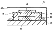
- FIG. 1 is a schematic cross-sectional view of one embodiment of the organic thin film transistor of the present invention.
- an organic thin film transistor 100 includes a substrate 10, a gate electrode 20 disposed on the substrate 10, a gate insulating film 30 covering the gate electrode 20, and a side of the gate insulating film 30 opposite to the gate electrode 20 side.
- a source electrode 40 and a drain electrode 42 in contact with the surface, an organic semiconductor film 50 covering the surface of the gate insulating film 30 between the source electrode 40 and the drain electrode 42, and a sealing layer 60 covering each member are provided.
- the organic semiconductor layer 50 is formed using the composition of the present invention described above.
- the organic thin film transistor 100 is a bottom contact type organic thin film transistor.
- the substrate plays a role of supporting a gate electrode, a source electrode, a drain electrode and the like which will be described later.
- substrate is not restrict
- a thermosetting resin for example, epoxy resin, phenol resin, polyimide resin, polyester resin (for example, PET, PEN)
- thermoplastic resin for example, phenoxy resin, polyether sulfone resin, polysulfone) Resin, polyphenylene sulfone resin, etc.
- Examples of the material for the ceramic substrate include alumina, aluminum nitride, zirconia, silicon, silicon nitride, silicon carbide, and the like.
- Examples of the glass substrate material include soda glass, potash glass, borosilicate glass, quartz glass, aluminum silicate glass, and lead glass.
- the gate electrode material e.g., gold (Au), silver, aluminum, copper, chromium, nickel, cobalt, titanium, platinum, magnesium, calcium, barium, such as sodium metal; InO 2, of SnO 2, ITO, etc.
- Examples include conductive oxides; conductive polymers such as polyaniline, polypyrrole, polythiophene, polyacetylene, and polydiacetylene; semiconductors such as silicon, germanium, and gallium arsenide; carbon materials such as fullerene, carbon nanotube, and graphite.
- the thickness of the gate electrode is not particularly limited, but is preferably 20 to 200 nm.
- the method for forming the gate electrode is not particularly limited, and examples thereof include a method of vacuum depositing or sputtering an electrode material on a substrate, and a method of applying or printing an electrode forming composition.
- examples of the patterning method include a photolithography method; a printing method such as ink jet printing, screen printing, offset printing, letterpress printing; and a mask vapor deposition method.
- ⁇ Gate insulation film Materials for the gate insulating film include polymethyl methacrylate, polystyrene, polyvinylphenol, polyimide, polycarbonate, polyester, polyvinyl alcohol, polyvinyl acetate, polyurethane, polysulfone, polybenzoxazole, polysilsesquioxane, epoxy resin, phenol Examples thereof include polymers such as resins; oxides such as silicon dioxide, aluminum oxide, and titanium oxide; and nitrides such as silicon nitride. Of these materials, a polymer is preferable in view of compatibility with the organic semiconductor layer.
- a crosslinking agent for example, melamine
- the polymer is crosslinked and the durability of the formed gate insulating film is improved.
- the thickness of the gate insulating film is not particularly limited, but is preferably 100 to 1000 nm.
- the method for forming the gate insulating film is not particularly limited, and examples thereof include a method for applying a gate insulating film forming composition on a substrate on which a gate electrode is formed, and a method for depositing or sputtering a gate insulating film material. It is done.
- the method for applying the gate insulating film forming composition is not particularly limited, and known methods (bar coating method, spin coating method, knife coating method, doctor blade method) can be used.
- a gate insulating film forming composition When a gate insulating film forming composition is applied to form a gate insulating film, it may be heated (baked) after application for the purpose of solvent removal, crosslinking, and the like.
- ⁇ Source electrode, drain electrode> Specific examples of the material of the source electrode and the drain electrode are the same as those of the gate electrode described above. Among these, a metal is preferable, and gold is more preferable.
- the method for forming the source electrode and the drain electrode is not particularly limited. For example, a method of vacuum-depositing or sputtering an electrode material on a substrate on which a gate electrode and a gate insulating film are formed, or applying or forming an electrode-forming composition Examples include a printing method. A specific example of the patterning method is the same as that of the gate electrode described above.
- the channel length of the source electrode and the drain electrode is not particularly limited, but is preferably 5 to 30 ⁇ m.
- the channel width of the source electrode and the drain electrode is not particularly limited, but is preferably 10 to 200 ⁇ m.
- the organic semiconductor layer is a layer formed using the above-described organic semiconductor composition of the present invention.
- the thickness of the organic semiconductor layer is not particularly limited, but is preferably 10 to 200 nm.
- the method for forming the organic semiconductor layer is not particularly limited, and examples thereof include a method of applying an organic semiconductor composition onto a substrate on which a gate electrode, a gate insulating film, a source electrode, and a drain electrode are formed.
- coating an organic-semiconductor composition is the same as the method of apply
- an organic semiconductor composition When an organic semiconductor composition is applied to form an organic semiconductor layer, it may be heated (baked) after application for the purpose of solvent removal, crosslinking and the like.
- the organic thin film transistor of the present invention preferably includes a sealing layer as the outermost layer from the viewpoint of durability.
- a well-known sealing agent can be used for a sealing layer.
- the thickness of the sealing layer is not particularly limited, but is preferably 0.2 to 10 ⁇ m.
- the method for forming the sealing layer is not particularly limited.
- the composition for forming the sealing layer is applied onto the substrate on which the gate electrode, the gate insulating film, the source electrode, the drain electrode, and the organic semiconductor layer are formed.
- the method etc. are mentioned.
- a specific example of the method of applying the sealing layer forming composition is the same as the method of applying the gate insulating film forming composition.
- the composition for forming a sealing layer is applied to form an organic semiconductor layer, it may be heated (baked) after application for the purpose of solvent removal, crosslinking, and the like.
- FIG. 2 is a schematic cross-sectional view of another embodiment of the organic thin film transistor of the present invention.
- the organic thin film transistor 200 includes a substrate 10, a gate electrode 20 disposed on the substrate 10, a gate insulating film 30 covering the gate electrode 20, and an organic semiconductor film 50 disposed on the gate insulating film 30.
- a source electrode 40 and a drain electrode 42 disposed on the organic semiconductor film 50 and a sealing layer 60 covering each member are provided.
- the organic semiconductor layer 50 is formed using the composition of the present invention described above.
- the organic thin film transistor 200 is a top contact type organic thin film transistor.
- the substrate, gate electrode, gate insulating film, source electrode, drain electrode, organic semiconductor layer, and sealing layer are as described above.
- the composition of the present invention has a top gate-bottom contact type.
- the present invention can also be applied to organic thin film transistors and top gate-top contact type organic thin film transistors.
- Organic semiconductor material “a-1” TIPS pentacene (6,13-bis (triisopropylsilylethynyl) pentacene, manufactured by Sigma-Aldrich)
- A-2 diF-TES-ADT (2,8-difluoro-5,11-bis (triethylsilylethynyl) anthradithiophene, manufactured by Sigma-Aldrich)
- A-3 PBTTTT-C12 (poly [2,5-bis (3-dodecylthiophen-2-yl) thieno [3,2-b] thiophene], manufactured by Sigma-Aldrich)
- A-4 P3HT (poly (3-hexylthiophene), manufactured by Sigma-Aldrich)
- B Migration inhibitor “b-1”: IRGANOX-245 (manufactured by BASF)
- V-1 was used instead of V-18 in DM-2.
- B-5 a fourth generation polymer having the same structure as DM-4 described in paragraph 0030 of JP-A-2005-227441 (Mw: 7500)
- B-6 IRGANOX-1076 (manufactured by BASF)
- B-7 BHT (2,6-di-tert-butyl-p-cresol, manufactured by Wako Pure Chemical Industries, Ltd.)
- B-8 IRGANOX-1330 (manufactured by BASF)
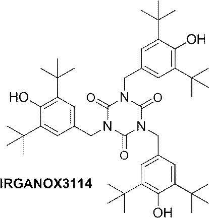
- B-9 IRGANOX-3114 (BASF)
- Example 1 (Preparation of organic semiconductor composition)
- Organic semiconductor concentration: 1.5% by mass) an organic semiconductor composition was prepared.
- the obtained organic semiconductor composition is designated as Composition 1.
- Al serving as a gate electrode was deposited on a glass substrate (Eagle XG: Corning) (thickness: 50 nm).
- baking was performed at 150 ° C. for 60 minutes to form a gate insulating film having a thickness of 400 nm.
- Au was vapor-deposited on the mask to form a source electrode and a drain electrode having a channel length of 25 ⁇ m and a channel width of 180 ⁇ m.
- the composition 1 was spin coated thereon and baked at 140 ° C. for 15 minutes to form an organic semiconductor layer having a thickness of 100 nm.
- Cytop CTL-107MK manufactured by AGC
- encapsulation layer forming composition was spin-coated and baked at 140 ° C. for 20 minutes to form a 2 ⁇ m-thick sealing layer (uppermost layer).
- An organic thin film transistor (bottom contact type) was obtained. This manufacturing method is referred to as a device manufacturing method 1.
- Each electrode of the obtained organic thin film transistor was connected to each terminal of a manual prober connected to a semiconductor parameter analyzer (4155C, manufactured by Agilent Technologies) to evaluate a field effect transistor (FET).
- FET field effect transistor
- field effect mobility [cm 2 / V ⁇ sec]
- Id-Vg drain current-gate voltage
- the calculated field effect mobility is defined as ⁇ 1.
- an organic thin film transistor was produced according to the same procedure as the production of the organic thin film transistor of Example 1 except that the comparative composition was used instead of the composition 1.
- T1 / T2 was calculated from the calculated T1 and T2, and evaluated according to the following criteria. The results are shown in Table 1. From the viewpoint of insulation reliability, it is preferably A to C, more preferably A or B, and even more preferably A. “A”: T1 / T2 ⁇ 5 “B”: 5> T1 / T2 ⁇ 2 “C”: 2> T1 / T2> 1 “D”: 0.1 ⁇ T1 / T2
- Example 2 An organic thin film transistor was produced in the same procedure as in Example 1 except that the following element production method 2 was carried out instead of the above-described element production method 1, and various evaluations were performed in accordance with the same procedure as in Example 1. . The results are summarized in Table 1.
- Examples 3 to 14, Comparative Examples 1 to 3> For Examples 3 to 14 and Comparative Examples 1 to 3, the organic semiconductor concentrations and solvents were the same as in Composition 1, and organic semiconductor materials a-1 to a-4 and migration inhibitors b-1 to b-9 were added. Each composition was prepared by mixing at a mixing ratio shown in Table 1. Using the compositions obtained in Examples 3 to 14 and Comparative Examples 1 to 3, as shown in Table 1, organic thin film transistors were prepared according to Element Preparation Method 1 or Element Preparation Method 2, and various evaluations were performed. . The results are summarized in Table 1. When performing the above evaluation, Examples 1 to 4 and 13 to 14 use a-1 as an organic semiconductor material in the comparative composition, Examples 5 and 6 use a-2, In Examples 7 and 8, a-3 was used, and in Examples 9 to 12, a-4 was used.
- (A) / (B) mass ratio indicates a mass ratio of “(A) organic semiconductor material” and “(B) migration inhibitor”.
- Substrate 20 Gate electrode 30: Gate insulating film 40: Source electrode 42: Drain electrode 50: Organic semiconductor layer 60: Sealing layer 100, 200: Organic thin film transistor
Abstract
Description
昨今、有機薄膜トランジスタへの期待が高まるなか、有機薄膜トランジスタには、移動度(特に電界効果移動度)の向上や安定性などが求められている。
このようななか、特許文献1には、有機半導体層の酸化劣化を低減するために、酸化防止剤を含有する組成物で有機半導体層を形成した有機薄膜トランジスタが開示されている。より具体的には、特許文献1の実施例欄においては、ヒンダードフェノール系酸化防止剤(長瀬産業社製:イルガノックス1076)や、2,2'-メチレンビス(6-tert-ブチル-p-クレゾール(住友化学社製:スミライザーMDP-S)などが使用されている。 Organic semiconductor materials can be used in devices that use logic circuits such as TFTs (thin film transistors), RFIDs (RF tags) and memories used in liquid crystal displays and organic EL displays because they can be reduced in weight, cost, and flexibility. An organic semiconductor device having an organic semiconductor film (organic semiconductor layer) made of is used.
In recent years, expectations for organic thin film transistors are increasing, and organic thin film transistors are required to have improved mobility (particularly field effect mobility) and stability.
Under such circumstances, Patent Document 1 discloses an organic thin film transistor in which an organic semiconductor layer is formed of a composition containing an antioxidant in order to reduce oxidative degradation of the organic semiconductor layer. More specifically, in the Example column of Patent Document 1, a hindered phenolic antioxidant (manufactured by Nagase Sangyo Co., Ltd .: Irganox 1076) and 2,2′-methylenebis (6-tert-butyl-p- Cresol (Sumitomo Chemical Co., Ltd .: Sumilizer MDP-S) is used.
本発明者らが特許文献1で具体的に開示される上述した酸化防止剤を含む組成物を用いて有機薄膜トランジスタを作製したところ、有機薄膜トランジスタの移動度、および/または、ソース電極/ドレイン電極間の絶縁信頼性は昨今求められるレベルを満たすものではないことが明らかとなった。 On the other hand, in recent years, there has been a demand for further improvement in the performance of organic thin film transistors, and in particular, there has been a demand for further improving the insulation reliability between the source electrode and the drain electrode without lowering the mobility. .
When the present inventors produced an organic thin film transistor using the above-described composition containing the antioxidant specifically disclosed in Patent Document 1, the mobility of the organic thin film transistor and / or between the source electrode and the drain electrode It became clear that the insulation reliability does not meet the level required recently.
すなわち、本発明者らは、以下の構成により上記課題が解決できることを見出した。 As a result of intensive studies on the above problems, the present inventors have found that a predetermined effect can be obtained by blending an organic semiconductor composition with a migration inhibitor represented by a predetermined structural formula, leading to the present invention. It was.
That is, the present inventors have found that the above problem can be solved by the following configuration.
後述する一般式(A)で表される基および後述する一般式(B)で表される基からなる群から選択される基を少なくとも2つ以上を含む化合物X、並びに、後述する一般式(C)で表される化合物Yのうち少なくともいずれか一方を含むマイグレーション防止剤と、を含む有機半導体組成物。
(2) 化合物Xおよび化合物Yの分子量が3000以下である、(1)に記載の有機半導体組成物。
(3) マイグレーション防止剤が、後述する一般式(D)で表される化合物である、(1)または(2)に記載の有機半導体組成物。
(4) 一般式(D)中のLが、後述する一般式(1)~一般式(10)で表される基からなる群から選択されるいずれか一つである、(3)に記載の有機半導体組成物。
(5) マイグレーション防止剤が化合物Xであり、
化合物X中に含まれる一般式(A)で表される基および一般式(B)で表される基の合計数が3以上である、(1)または(2)に記載の有機半導体組成物。
(6) (1)~(5)のいずれかに記載の有機半導体組成物を使用して作製される有機半導体層。
(7) (1)~(5)のいずれかに記載の有機半導体組成物を使用して作製される有機半導体層と、ソース電極と、ドレイン電極と、ゲート電極とを含む有機薄膜トランジスタ。
(8) ソース電極、ドレイン電極、および、ゲート電極からなる群から選択される少なくとも1つが銀を含む、(7)に記載の有機薄膜トランジスタ。
(9) (7)または(8)に記載の有機薄膜トランジスタを含む電子ペーパー。
(10) (7)または(8)に記載の有機薄膜トランジスタを含むディスプレイデバイス。 (1) Organic semiconductor materials,
A compound X containing at least two groups selected from the group consisting of a group represented by general formula (A) described later and a group represented by general formula (B) described later, and a general formula (described later) An organic semiconductor composition comprising a migration inhibitor containing at least one of compounds Y represented by C).
(2) The organic semiconductor composition according to (1), wherein the molecular weight of compound X and compound Y is 3000 or less.
(3) The organic semiconductor composition according to (1) or (2), wherein the migration inhibitor is a compound represented by the general formula (D) described later.
(4) The L in the general formula (D) is any one selected from the group consisting of groups represented by the general formula (1) to the general formula (10) described later, (3) Organic semiconductor composition.
(5) The migration inhibitor is Compound X,
The organic semiconductor composition according to (1) or (2), wherein the total number of the group represented by the general formula (A) and the group represented by the general formula (B) contained in the compound X is 3 or more. .
(6) An organic semiconductor layer produced using the organic semiconductor composition according to any one of (1) to (5).
(7) An organic thin film transistor comprising an organic semiconductor layer produced using the organic semiconductor composition according to any one of (1) to (5), a source electrode, a drain electrode, and a gate electrode.
(8) The organic thin film transistor according to (7), wherein at least one selected from the group consisting of a source electrode, a drain electrode, and a gate electrode contains silver.
(9) Electronic paper including the organic thin film transistor according to (7) or (8).
(10) A display device comprising the organic thin film transistor according to (7) or (8).
本発明の有機半導体組成物(以下、単に「組成物」とも称する。)は、有機半導体材料と、所定の化合物より選択されるマイグレーション防止剤(マイグレーション抑制剤)とを含有する。
本発明の従来技術と比較した特徴点は、所定の化合物より選択されるマイグレーション防止剤を使用している点が挙げられる。このマイグレーション防止剤を使用することにより、有機半導体層中におけるマイグレーション防止剤の分散性が向上するとともに、有機半導体の結晶化の阻害がより抑制され、結果として移動度と絶縁信頼性とが優れる有機薄膜トランジスタが得られる。
以下、組成物中に含まれる各成分について詳述する。まず、有機半導体材料について詳述し、その後マイグレーション防止剤について詳述する。 Below, the suitable aspect of the organic-semiconductor composition (composition for organic semiconductors. Composition for organic-semiconductor-layer formation) and organic thin-film transistor (organic-semiconductor transistor) of this invention is demonstrated.
The organic semiconductor composition of the present invention (hereinafter also simply referred to as “composition”) contains an organic semiconductor material and a migration inhibitor (migration inhibitor) selected from predetermined compounds.
The feature point compared with the prior art of the present invention is that a migration inhibitor selected from predetermined compounds is used. By using this migration inhibitor, the dispersibility of the migration inhibitor in the organic semiconductor layer is improved, and inhibition of crystallization of the organic semiconductor is further suppressed. As a result, an organic material having excellent mobility and insulation reliability. A thin film transistor is obtained.
Hereinafter, each component contained in the composition will be described in detail. First, the organic semiconductor material will be described in detail, and then the migration inhibitor will be described in detail.
本発明の組成物に含有される有機半導体材料としては、有機薄膜トランジスタの有機半導体層として利用される、公知の材料が利用可能である。具体的には、6,13-ビス(トリイソプロピルシリルエチニル)ペンタセン(TIPSペンタセン)、テトラメチルペンタセン、パーフルオロペンタセン等のペンタセン類、TES-ADT、diF-TES-ADT等のアントラジチオフェン類、DPh-BTBT、Cn-BTBT等のベンゾチエノベンゾチオフェン類、Cn-DNTT等のジナフトチエノチオフェン類、ペリキサンテノキサンテン等のジオキサアンタントレン類、ルブレン類、C60、PCBM等のフラーレン類、銅フタロシアニン、フッ素化銅フタロシアニン等のフタロシアニン類、P3RT、PQT、P3HT、PQT等のポリチオフェン類、ポリ[2,5-ビス(3-ドデシルチオフェン-2-イル)チエノ[3,2-b]チオフェン](PBTTT)等のポリチエノチオフェン類等が例示される。 <Organic semiconductor materials>
As the organic semiconductor material contained in the composition of the present invention, a known material used as an organic semiconductor layer of an organic thin film transistor can be used. Specifically, pentacenes such as 6,13-bis (triisopropylsilylethynyl) pentacene (TIPS pentacene), tetramethylpentacene and perfluoropentacene, anthradithiophenes such as TES-ADT and diF-TES-ADT, Benzothienobenzothiophenes such as DPh-BTBT and Cn-BTBT, dinaphthothienothiophenes such as Cn-DNTT, dioxaanthanthrenes such as perixanthenoxanthene, rubrenes, fullerenes such as C60 and PCBM, copper Phthalocyanines such as phthalocyanine and fluorinated copper phthalocyanine, polythiophenes such as P3RT, PQT, P3HT and PQT, poly [2,5-bis (3-dodecylthiophen-2-yl) thieno [3,2-b] thiophene] Poly (PBTT) etc. Eno thiophenes and the like.
本発明の組成物に含有されるマイグレーション防止剤としては、以下の化合物Xおよび化合物Yから選択される化合物が挙げられる。
化合物X:一般式(A)で表される基および一般式(B)で表される基からなる群から選択される基を少なくとも2つ以上を含む化合物
化合物Y:一般式(C)で表される化合物
以下、式中の各基について説明する。 <Migration inhibitor>
Examples of the migration inhibitor contained in the composition of the present invention include compounds selected from the following compounds X and Y.
Compound X: Compound containing at least two groups selected from the group consisting of groups represented by general formula (A) and groups represented by general formula (B) Compound Y: represented by general formula (C) Hereinafter, each group in the formula will be described.

置換基としては、ハロゲン原子、アルキル基(シクロアルキル基を含む)、アルケニル基(シクロアルケニル基、ビシクロアルケニル基を含む)、アルキニル基、アリール基、複素環基、シアノ基、ヒドロキシル基、ニトロ基、カルボキシル基、アルコキシ基、アリールオキシ基、シリルオキシ基、複素環オキシ基、アシルオキシ基、カルバモイルオキシ基、アルコキシカルボニルオキシ基、アリールオキシカルボニルオキシ基、アミノ基(アニリノ基を含む)、アシルアミノ基、アミノカルボニルアミノ基、アルコキシカルボニルアミノ基、アリールオキシカルボニルアミノ基、スルファモイルアミノ基、アルキルおよびアリールスルホニルアミノ基、メルカプト基、アルキルチオ基、アリールチオ基、複素環チオ基、スルファモイル基、スルホ基、アルキルおよびアリールスルフィニル基、アルキルおよびアリールスルホニル基、アシル基、アリールオキシカルボニル基、アルコキシカルボニル基、カルバモイル基、アリールおよび複素環アゾ基、イミド基、ホスフィノ基、ホスフィニル基、ホスフィニルオキシ基、ホスフィニルアミノ基、シリル基、またはこれらの組み合わせが挙げられる。 In general formula (A), R 1 to R 3 each independently represents a hydrogen atom or a substituent.
Substituents include halogen atoms, alkyl groups (including cycloalkyl groups), alkenyl groups (including cycloalkenyl groups and bicycloalkenyl groups), alkynyl groups, aryl groups, heterocyclic groups, cyano groups, hydroxyl groups, and nitro groups. , Carboxyl group, alkoxy group, aryloxy group, silyloxy group, heterocyclic oxy group, acyloxy group, carbamoyloxy group, alkoxycarbonyloxy group, aryloxycarbonyloxy group, amino group (including anilino group), acylamino group, amino group Carbonylamino group, alkoxycarbonylamino group, aryloxycarbonylamino group, sulfamoylamino group, alkyl and arylsulfonylamino group, mercapto group, alkylthio group, arylthio group, heterocyclic thio group, sulfamoyl group, Rufo group, alkyl and arylsulfinyl group, alkyl and arylsulfonyl group, acyl group, aryloxycarbonyl group, alkoxycarbonyl group, carbamoyl group, aryl and heterocyclic azo group, imide group, phosphino group, phosphinyl group, phosphinyloxy Group, phosphinylamino group, silyl group, or combinations thereof.
なお、R1とR2とが両方とも水素原子であることはない。
また、式中、*は結合位置を示す。 Among them, R 1 and R 2 are independently independent in that the mobility and / or insulation reliability of the obtained organic thin film transistor is more excellent (hereinafter, also simply referred to as “the effect of the present invention is more excellent”). A hydrogen atom, an alkyl group, or an alkoxy group is preferable, and an alkyl group having 1 to 4 carbon atoms is more preferable. In addition, R 3 is preferably a hydrogen atom or an alkyl group from the viewpoint that the effects of the present invention are more excellent.
Note that R 1 and R 2 are not both hydrogen atoms.
In the formula, * indicates a bonding position.
なかでも、本発明の効果がより優れる点で、R4はアルキル基、または、アルコキシ基であることが好ましく、炭素数1~4のアルキル基がより好ましい。
R5~R7は、それぞれ独立に、水素原子または置換基を表す。置換基の定義は、上述の通りである。
なかでも、本発明の効果がより優れる点で、R5およびR7は、それぞれ独立に、水素原子またはアルキル基であることが好ましい。
R6は水素原子、アルキル基、またはアルコキシ基であることが好ましく、炭素数1~4のアルキル基であることがより好ましい。 In general formula (B), R 4 represents a substituent. The definition of the substituent is as described above.
Among these, R 4 is preferably an alkyl group or an alkoxy group, more preferably an alkyl group having 1 to 4 carbon atoms, from the viewpoint that the effects of the present invention are more excellent.
R 5 to R 7 each independently represents a hydrogen atom or a substituent. The definition of the substituent is as described above.
Among them, in terms of the effect of the present invention is more excellent, R 5 and R 7 each independently is preferably a hydrogen atom or an alkyl group.
R 6 is preferably a hydrogen atom, an alkyl group, or an alkoxy group, more preferably an alkyl group having 1 to 4 carbon atoms.
*は結合位置を示す。 X represents a divalent linking group. Examples of the divalent linking group include a linear, branched, or cyclic divalent aliphatic hydrocarbon group (for example, an alkylene group having 1 to 12 carbon atoms. More specifically, a methylene group, an ethylene group, , Propylene group, etc.), linear, branched or cyclic divalent aromatic hydrocarbon group (eg, phenylene group), —O—, —S—, —SO 2 —, —NR 20 —, —CO —, —NH—, —COO—, —CONR 20 —, —O—CO—O—, —SO 3 —, —NHCOO—, —SO 2 NR 20 —, —NH—CO—NH—, or these A plurality of groups (for example, an alkyleneoxy group, an alkyleneoxycarbonyl group, an alkylenecarbonyloxy group, etc.) and the like can be mentioned. Here, R 20 represents a hydrogen atom or an alkyl group having 1 to 5 carbon atoms.
* Indicates a binding position.
なかでも、本発明の効果がより優れる点で、R8およびR12は、それぞれ独立に、アルキル基またはアルコキシ基であることが好ましく、炭素数1~4のアルキル基であることがより好ましい。
R9~R11およびR13~R15は、それぞれ独立に、水素原子または置換基を表す。置換基の定義は、上述の通りである。
なかでも、本発明の効果がより優れる点で、R9~R11およびR13~R15は、それぞれ独立に、水素原子またはアルキル基であることが好ましく、水素原子であることがより好ましい。
R9、R11、R13およびR15は、それぞれ独立に、水素原子またはアルキル基であることが好ましい。R10およびR14は、それぞれ独立に、水素原子、アルキル基またはアルコキシ基であることが好ましく、炭素数1~4のアルキル基であることがより好ましい。 In general formula (C), R 8 and R 12 each independently represent a substituent. The definition of the substituent is as described above.
Of these, R 8 and R 12 are each independently preferably an alkyl group or an alkoxy group, more preferably an alkyl group having 1 to 4 carbon atoms, from the viewpoint that the effects of the present invention are more excellent.
R 9 to R 11 and R 13 to R 15 each independently represents a hydrogen atom or a substituent. The definition of the substituent is as described above.
Of these, R 9 to R 11 and R 13 to R 15 are each independently preferably a hydrogen atom or an alkyl group, and more preferably a hydrogen atom, from the viewpoint that the effects of the present invention are more excellent.
R 9 , R 11 , R 13 and R 15 are preferably each independently a hydrogen atom or an alkyl group. R 10 and R 14 are each independently preferably a hydrogen atom, an alkyl group or an alkoxy group, more preferably an alkyl group having 1 to 4 carbon atoms.
なお、Rは、水素原子または置換基を表す。置換基の定義は、上述の通りである。Rとしては、水素原子またはアルキル基が好ましい。 Z represents —O—, —S—, —SO—, —SO 2 —, —NR—, —PR—, —POR—, —COCO—, —NHNH— or —S—S—.
R represents a hydrogen atom or a substituent. The definition of the substituent is as described above. R is preferably a hydrogen atom or an alkyl group.
また、本発明の効果がより優れる点で、化合物Xには一般式(A)で表される基が少なくとも含まれることが好ましく、特に、一般式(A)で表される基が上記好適範囲の数含まれることがより好ましい。 Compound X includes at least two groups selected from the group consisting of the group represented by the general formula (A) and the group represented by the general formula (B), and the effects of the present invention are more excellent. In view of this, it is preferable to include three or more, and more preferably four or more. The upper limit is not particularly limited, but is preferably 12 or less, more preferably 6 or less, from the viewpoint of synthesis.
Moreover, it is preferable that the group represented by general formula (A) is contained in compound X at the point which the effect of this invention is more excellent, and especially group represented by general formula (A) is the said suitable range. It is more preferable that the number is included.
化合物Xおよび化合物Yの分子量は特に制限されないが、本発明の効果がより優れる点で、3000以下が好ましく、2000以下がより好ましい。下限は特に制限されないが、有機半導体材料の結晶性の点からは、330以上が好ましく、500以上がより好ましい。 Compound X may be a high molecular compound or a low molecular compound. For example, the polymer compound may be a multi-branched polymer (hyperbranched polymer, dendrimer, etc.).
The molecular weights of Compound X and Compound Y are not particularly limited, but are preferably 3000 or less, more preferably 2000 or less, from the viewpoint that the effects of the present invention are more excellent. Although a minimum in particular is not restrict | limited, From the crystalline point of organic-semiconductor material, 330 or more are preferable and 500 or more are more preferable.
一般式(D) (Rx)n-L-(Ry)m
一般式(D)中、Rxは、一般式(E)で表される基、および、一般式(B)で表される基からなる群から選択される基である。一般式(B)で表される基の定義は、上述の通りである。
一般式(E)で表される基中のR1~R3の定義は、一般式(A)で表される基中の各基の定義と同義である。 As a suitable aspect of the said migration inhibitor, the compound represented by general formula (D) is mentioned by the point which the effect of this invention is more excellent.
Formula (D) (Rx) nL- (Ry) m
In general formula (D), Rx is a group selected from the group consisting of a group represented by general formula (E) and a group represented by general formula (B). The definition of group represented by general formula (B) is as above-mentioned.
The definitions of R 1 to R 3 in the group represented by the general formula (E) are the same as the definitions of each group in the group represented by the general formula (A).

*は結合位置を示す。ただし、R1とR2が両方とも水素原子になることはない。
また、nが2以上の場合、複数のRxは同一でも異なっていてもよい。 In general formula (E), Y represents a single bond or a divalent linking group. The definition of a bivalent coupling group is synonymous with the definition of the bivalent coupling group represented by X mentioned above. Preferred examples of Y include an alkylene group, an amide group, and -L 10 -L 11 -L 10- (L 10 : an alkylene group, L 11 : an ester group or an amide group). -O- may be included.
* Indicates a binding position. However, R 1 and R 2 are not both hydrogen atoms.
When n is 2 or more, the plurality of Rx may be the same or different.
なかでも、本発明の効果がより優れる点で、Ryは、水素原子、アルキル基またはアリール基であることが好ましい。mが2以上の場合、複数のRyは同一でも異なっていてもよい。 Ry represents a hydrogen atom or a substituent. The definition of the substituent is as described above.
Especially, it is preferable that Ry is a hydrogen atom, an alkyl group, or an aryl group at the point which the effect of this invention is more excellent. When m is 2 or more, the plurality of Ry may be the same or different.
Lの好適態様としては、本発明の効果がより優れる点で、一般式(1)~一般式(10)で表される基からなる群から選択される基が挙げられる。*は、結合位置を示す。
なお、一般式(1)、(2)、(8)および(9)の場合はn+m=2(nは2、mは0)であり、一般式(3)~(5)の場合はn+m=3(nは2~3、mは0~1)であり、一般式(6)の場合はn+m=4(nは2~4、mは0~2)であり、一般式(7)および(10)の場合はn+m=6(nは2~6、mは0~4)である。
なお、一般式(10)中、L1は、単結合または2価の連結基を表す。2価の連結基の定義は、Xで表される2価の連結基の定義と同義である。 L represents an n + m-valent linking group. For example, when n + m = 2, a divalent linking group is used, when n + m = 3, a trivalent linking group is used, when n + m = 4, a tetravalent linking group is used, and when n + m = 5, a pentavalent linking group is used. Group, and when n + m = 6, represents a hexavalent linking group.
Preferable embodiments of L include groups selected from the group consisting of groups represented by general formula (1) to general formula (10) in that the effects of the present invention are more excellent. * Indicates a binding position.
In the general formulas (1), (2), (8), and (9), n + m = 2 (n is 2, m is 0), and in the general formulas (3) to (5), n + m = 3 (n is 2 to 3, m is 0 to 1), and in the case of general formula (6), n + m = 4 (n is 2 to 4, m is 0 to 2), and general formula (7) In the case of (10), n + m = 6 (n is 2 to 6, m is 0 to 4).
In general formula (10), L 1 represents a single bond or a divalent linking group. The definition of a bivalent coupling group is synonymous with the definition of the bivalent coupling group represented by X.

なかでも、本発明の効果がより優れる点で、nは2~4の整数を表すことが好ましい。また、mは0~2の整数を表すことが好ましく、mは0が好ましい。
nとmとの関係の好適態様は、nは2~4の整数を表し、mは0~2の整数を表し、n+m≦4を満たす態様が挙げられる。 n represents an integer of 2 to 6, m represents an integer of 0 to 4, and satisfies n + m ≦ 6.
Among these, n is preferably an integer of 2 to 4 in that the effect of the present invention is more excellent. M is preferably an integer of 0 to 2, and m is preferably 0.
Preferred embodiments of the relationship between n and m include an embodiment in which n represents an integer of 2 to 4, m represents an integer of 0 to 2, and satisfies n + m ≦ 4.


溶媒としては特に制限されないが、例えば、トルエン、キシレン、メシチレン、1,2,3,4-テトラヒドロナフタレン(テトラリン)、クロロベンゼン、ジクロロベンゼン、アニソールなどの芳香族化合物が好適に例示される。 The composition of the present invention preferably contains a solvent from the viewpoint of homogeneity and crystallinity of the organic semiconductor layer to be formed.
Although it does not restrict | limit especially as a solvent, For example, aromatic compounds, such as toluene, xylene, mesitylene, 1,2,3,4-tetrahydronaphthalene (tetralin), chlorobenzene, dichlorobenzene, anisole, are illustrated suitably.
本発明の有機薄膜トランジスタは、上述した本発明の組成物より形成される有機半導体層に用いた有機薄膜トランジスタである。なかでも、ボトムコンタクト型の有機薄膜トランジスタであることが好ましい。 [Organic thin film transistor]
The organic thin-film transistor of this invention is an organic thin-film transistor used for the organic-semiconductor layer formed from the composition of this invention mentioned above. Especially, it is preferable that it is a bottom contact type organic thin-film transistor.
図1は、本発明の有機薄膜トランジスタの一態様の断面模式図である。
図1において、有機薄膜トランジスタ100は、基板10と、基板10上に配置されたゲート電極20と、ゲート電極20を覆うゲート絶縁膜30と、ゲート絶縁膜30のゲート電極20側とは反対側の表面に接するソース電極40およびドレイン電極42と、ソース電極40とドレイン電極42との間のゲート絶縁膜30の表面を覆う有機半導体膜50と、各部材を覆う封止層60とを備える。ここで、有機半導体層50は、上述した本発明の組成物を用いて形成されたものである。有機薄膜トランジスタ100は、ボトムコンタクト型の有機薄膜トランジスタである。 One embodiment of the organic thin film transistor of the present invention will be described with reference to the drawings.
FIG. 1 is a schematic cross-sectional view of one embodiment of the organic thin film transistor of the present invention.
In FIG. 1, an organic
基板は、後述するゲート電極、ソース電極、ドレイン電極などを支持する役割を果たす。
基板の種類は特に制限されず、例えば、プラスチック基板、ガラス基板、セラミック基板などが挙げられる。なかでも、各デバイスへの適用性およびコストの観点から、ガラス基板またはプラスチック基板であることが好ましい。
プラスチック基板の材料としては、熱硬化性樹脂(例えば、エポキシ樹脂、フェノール樹脂、ポリイミド樹脂、ポリエステル樹脂(例えばPET、PEN)など)または熱可塑性樹脂(例えば、フェノキシ樹脂、ポリエーテルスルフォン樹脂、ポリスルフォン樹脂、ポリフェニレンスルフォン樹脂など)が挙げられる。
セラミック基板の材料としては、例えば、アルミナ、窒化アルミニウム、ジルコニア、シリコン、窒化シリコン、シリコンカーバイドなどが挙げられる。
ガラス基板の材料としては、例えば、ソーダガラス、カリガラス、ホウケイ酸ガラス、石英ガラス、アルミケイ酸ガラス、鉛ガラスなどが挙げられる。 <Board>
The substrate plays a role of supporting a gate electrode, a source electrode, a drain electrode and the like which will be described later.
The kind of board | substrate is not restrict | limited in particular, For example, a plastic substrate, a glass substrate, a ceramic substrate etc. are mentioned. Among these, a glass substrate or a plastic substrate is preferable from the viewpoint of applicability to each device and cost.
As a material of the plastic substrate, a thermosetting resin (for example, epoxy resin, phenol resin, polyimide resin, polyester resin (for example, PET, PEN)) or thermoplastic resin (for example, phenoxy resin, polyether sulfone resin, polysulfone) Resin, polyphenylene sulfone resin, etc.).
Examples of the material for the ceramic substrate include alumina, aluminum nitride, zirconia, silicon, silicon nitride, silicon carbide, and the like.
Examples of the glass substrate material include soda glass, potash glass, borosilicate glass, quartz glass, aluminum silicate glass, and lead glass.
ゲート電極の材料としては、例えば、金(Au)、銀、アルミニウム、銅、クロム、ニッケル、コバルト、チタン、白金、マグネシウム、カルシウム、バリウム、ナトリウム等の金属;InO2、SnO2、ITO等の導電性の酸化物;ポリアニリン、ポリピロール、ポリチオフェン、ポリアセチレン、ポリジアセチレン等の導電性高分子;シリコン、ゲルマニウム、ガリウム砒素等の半導体;フラーレン、カーボンナノチューブ、グラファイト等の炭素材料などが挙げられる。なかでも、金属であることが好ましく、銀、アルミニウムであることがより好ましい。 <Gate electrode>
The gate electrode material, e.g., gold (Au), silver, aluminum, copper, chromium, nickel, cobalt, titanium, platinum, magnesium, calcium, barium, such as sodium metal; InO 2, of SnO 2, ITO, etc. Examples include conductive oxides; conductive polymers such as polyaniline, polypyrrole, polythiophene, polyacetylene, and polydiacetylene; semiconductors such as silicon, germanium, and gallium arsenide; carbon materials such as fullerene, carbon nanotube, and graphite. Especially, it is preferable that it is a metal, and it is more preferable that they are silver and aluminum.
ゲート絶縁膜の材料としては、ポリメチルメタクリレート、ポリスチレン、ポリビニルフェノール、ポリイミド、ポリカーボネート、ポリエステル、ポリビニルアルコール、ポリ酢酸ビニル、ポリウレタン、ポリスルフォン、ポリベンゾキサゾール、ポリシルセスキオキサン、エポキシ樹脂、フェノール樹脂等のポリマー;二酸化珪素、酸化アルミニウム、酸化チタン等の酸化物;窒化珪素等の窒化物などが挙げられる。これらの材料のうち、有機半導体層との相性から、ポリマーであることが好ましい。
ゲート絶縁膜の材料としてポリマーを用いる場合、架橋剤(例えば、メラミン)を併用するのが好ましい。架橋剤を併用することで、ポリマーが架橋されて、形成されるゲート絶縁膜の耐久性が向上する。 <Gate insulation film>
Materials for the gate insulating film include polymethyl methacrylate, polystyrene, polyvinylphenol, polyimide, polycarbonate, polyester, polyvinyl alcohol, polyvinyl acetate, polyurethane, polysulfone, polybenzoxazole, polysilsesquioxane, epoxy resin, phenol Examples thereof include polymers such as resins; oxides such as silicon dioxide, aluminum oxide, and titanium oxide; and nitrides such as silicon nitride. Of these materials, a polymer is preferable in view of compatibility with the organic semiconductor layer.
When a polymer is used as the material for the gate insulating film, it is preferable to use a crosslinking agent (for example, melamine) in combination. By using a crosslinking agent in combination, the polymer is crosslinked and the durability of the formed gate insulating film is improved.
ゲート絶縁膜形成用組成物を塗布してゲート絶縁膜を形成する場合、溶媒除去、架橋などを目的として、塗布後に加熱(ベーク)してもよい。 The method for forming the gate insulating film is not particularly limited, and examples thereof include a method for applying a gate insulating film forming composition on a substrate on which a gate electrode is formed, and a method for depositing or sputtering a gate insulating film material. It is done. The method for applying the gate insulating film forming composition is not particularly limited, and known methods (bar coating method, spin coating method, knife coating method, doctor blade method) can be used.
When a gate insulating film forming composition is applied to form a gate insulating film, it may be heated (baked) after application for the purpose of solvent removal, crosslinking, and the like.
ソース電極およびドレイン電極の材料の具体例は、上述したゲート電極と同じである。なかでも、金属であることが好ましく、金であることがより好ましい。
ソース電極およびドレイン電極を形成する方法は特に制限されないが、例えば、ゲート電極とゲート絶縁膜とが形成された基板上に、電極材料を真空蒸着またはスパッタする方法、電極形成用組成物を塗布または印刷する方法などが挙げられる。パターニング方法の具体例は、上述したゲート電極と同じである。
ソース電極およびドレイン電極のチャネル長は特に制限されないが、5~30μmであることが好ましい。
ソース電極およびドレイン電極のチャネル幅は特に制限されないが、10~200μmであることが好ましい。 <Source electrode, drain electrode>
Specific examples of the material of the source electrode and the drain electrode are the same as those of the gate electrode described above. Among these, a metal is preferable, and gold is more preferable.
The method for forming the source electrode and the drain electrode is not particularly limited. For example, a method of vacuum-depositing or sputtering an electrode material on a substrate on which a gate electrode and a gate insulating film are formed, or applying or forming an electrode-forming composition Examples include a printing method. A specific example of the patterning method is the same as that of the gate electrode described above.
The channel length of the source electrode and the drain electrode is not particularly limited, but is preferably 5 to 30 μm.
The channel width of the source electrode and the drain electrode is not particularly limited, but is preferably 10 to 200 μm.
有機半導体層は、上述した本発明の有機半導体組成物を用いて形成した層である。
有機半導体層の厚みは特に制限されないが、10~200nmであることが好ましい。 <Organic semiconductor layer>
The organic semiconductor layer is a layer formed using the above-described organic semiconductor composition of the present invention.
The thickness of the organic semiconductor layer is not particularly limited, but is preferably 10 to 200 nm.
本発明の有機薄膜トランジスタは、耐久性の観点から、最外層に封止層を備えるのが好ましい。封止層には公知の封止剤を用いることができる。
封止層の厚みは特に制限されないが、0.2~10μmであることが好ましい。 <Sealing layer>
The organic thin film transistor of the present invention preferably includes a sealing layer as the outermost layer from the viewpoint of durability. A well-known sealing agent can be used for a sealing layer.
The thickness of the sealing layer is not particularly limited, but is preferably 0.2 to 10 μm.
図2において、有機薄膜トランジスタ200は、基板10と、基板10上に配置されたゲート電極20と、ゲート電極20を覆うゲート絶縁膜30と、ゲート絶縁膜30上に配置された有機半導体膜50と、有機半導体膜50上に配置されたソース電極40およびドレイン電極42と、各部材を覆う封止層60を備える。ここで、有機半導体層50は、上述した本発明の組成物を用いて形成されたものである。有機薄膜トランジスタ200は、トップコンタクト型の有機薄膜トランジスタである。
基板、ゲート電極、ゲート絶縁膜、ソース電極、ドレイン電極、有機半導体層および封止層については上述のとおりである。 FIG. 2 is a schematic cross-sectional view of another embodiment of the organic thin film transistor of the present invention.
2, the organic
The substrate, gate electrode, gate insulating film, source electrode, drain electrode, organic semiconductor layer, and sealing layer are as described above.
(A)有機半導体材料
「a-1」:TIPSペンタセン(6,13-ビス(トリイソプロピルシリルエチニル)ペンタセン、Sigma-Aldrich社製)
「a-2」:diF-TES-ADT(2,8-ジフルオロ-5,11-ビス(トリエチルシリルエチニル)アントラジチオフェン、Sigma-Aldrich社製)
「a-3」:PBTTT-C12(ポリ[2,5-ビス(3-ドデシルチオフェン-2-イル)チエノ[3,2-b]チオフェン]、Sigma-Aldrich社製)
「a-4」:P3HT(ポリ(3-ヘキシルチオフェン)、Sigma-Aldrich社製)
(B)マイグレーション防止剤
「b-1」:IRGANOX-245(BASF社製)
「b-2」:IRGANOX-1035(BASF社製)
「b-3」:IRGANOX-1010(BASF社製)
「b-4」:特開2005-227441の段落0028に記載のDM-2と同構造を有する第二世代ポリマー(Mw:1800)。ただし、本件では上記DM-2中のV-18の代わりに、V-1を使用した。
「b-5」:特開2005-227441の段落0030に記載のDM-4と同構造を有する第四世代ポリマー(Mw:7500)
「b-6」:IRGANOX-1076(BASF社製)
「b-7」:BHT(2,6-ジ-tert-ブチル-p-クレゾール、和光純薬社製)
「b-8」:IRGANOX-1330(BASF社製)
「b-9」:IRGANOX-3114(BASF社製) In Examples and Comparative Examples described later, organic semiconductor materials and migration inhibitors exemplified below were used.
(A) Organic semiconductor material “a-1”: TIPS pentacene (6,13-bis (triisopropylsilylethynyl) pentacene, manufactured by Sigma-Aldrich)
“A-2”: diF-TES-ADT (2,8-difluoro-5,11-bis (triethylsilylethynyl) anthradithiophene, manufactured by Sigma-Aldrich)
“A-3”: PBTTTT-C12 (poly [2,5-bis (3-dodecylthiophen-2-yl) thieno [3,2-b] thiophene], manufactured by Sigma-Aldrich)
“A-4”: P3HT (poly (3-hexylthiophene), manufactured by Sigma-Aldrich)
(B) Migration inhibitor “b-1”: IRGANOX-245 (manufactured by BASF)
“B-2”: IRGANOX-1035 (BASF)
“B-3”: IRGANOX-1010 (manufactured by BASF)
“B-4”: a second generation polymer (Mw: 1800) having the same structure as DM-2 described in paragraph 0028 of JP-A-2005-227441. However, in this case, V-1 was used instead of V-18 in DM-2.
“B-5”: a fourth generation polymer having the same structure as DM-4 described in paragraph 0030 of JP-A-2005-227441 (Mw: 7500)
“B-6”: IRGANOX-1076 (manufactured by BASF)
“B-7”: BHT (2,6-di-tert-butyl-p-cresol, manufactured by Wako Pure Chemical Industries, Ltd.)
“B-8”: IRGANOX-1330 (manufactured by BASF)
“B-9”: IRGANOX-3114 (BASF)


(有機半導体組成物の調製)
上記有機半導体材料a-1と上記マイグレーション防止剤b-1とをトルエンに溶解させて(有機半導体材料a-1/マイグレーション防止剤b-1=100質量部/50質量部(w/w)、有機半導体濃度:1.5質量%)、有機半導体組成物を調製した。得られた有機半導体組成物を組成物1とする。 <Example 1>
(Preparation of organic semiconductor composition)
The organic semiconductor material a-1 and the migration inhibitor b-1 are dissolved in toluene (organic semiconductor material a-1 / migration inhibitor b-1 = 100 parts by mass / 50 parts by mass (w / w)) Organic semiconductor concentration: 1.5% by mass), an organic semiconductor composition was prepared. The obtained organic semiconductor composition is designated as Composition 1.
ガラス基板(イーグルXG:コーニング社製)上に、ゲート電極となるAlを蒸着した(厚み:50nm)。その上にゲート絶縁膜形成用組成物(ポリビニルフェノール/メラミン=1質量部/1質量部(w/w)のPGMEA(プロピレングリコールモノメチルエーテルアセテート)溶液(溶液濃度:2質量%))をスピンコートし、150℃で60分間ベークを行い、膜厚400nmのゲート絶縁膜を形成した。その上にAuをマスク蒸着し、チャネル長25μm、チャネル幅180μmのソース電極およびドレイン電極を形成した。その上に上記組成物1をスピンコートし、140℃で15分間ベークを行い、厚み100nmの有機半導体層を形成した。その上にCytop CTL-107MK(AGC社製)(封止層形成用組成物)をスピンコートし、140℃で20分間ベークを行い、厚み2μmの封止層(最上層)を形成して、有機薄膜トランジスタ(ボトムコンタクト型)を得た。
本作製方法を素子作製方法1とする。 (Preparation of organic thin film transistor (Element preparation method 1))
Al serving as a gate electrode was deposited on a glass substrate (Eagle XG: Corning) (thickness: 50 nm). On top of that, a composition for forming a gate insulating film (polyvinylphenol / melamine = 1 part by weight / 1 part by weight (w / w) PGMEA (propylene glycol monomethyl ether acetate) solution (solution concentration: 2% by weight)) is spin-coated. Then, baking was performed at 150 ° C. for 60 minutes to form a gate insulating film having a thickness of 400 nm. Au was vapor-deposited on the mask to form a source electrode and a drain electrode having a channel length of 25 μm and a channel width of 180 μm. The composition 1 was spin coated thereon and baked at 140 ° C. for 15 minutes to form an organic semiconductor layer having a thickness of 100 nm. On top of this, Cytop CTL-107MK (manufactured by AGC) (encapsulation layer forming composition) was spin-coated and baked at 140 ° C. for 20 minutes to form a 2 μm-thick sealing layer (uppermost layer). An organic thin film transistor (bottom contact type) was obtained.
This manufacturing method is referred to as a device manufacturing method 1.
得られた有機薄膜トランジスタの各電極と、半導体パラメータ・アナライザ(4155C、Agilent Technologies社製)に接続されたマニュアルプローバの各端子とを接続して、電界効果トランジスタ(FET)の評価を行なった。具体的には、ドレイン電流-ゲート電圧(Id‐Vg)特性を測定することにより電界効果移動度([cm2/V・sec])を算出した。算出した電界効果移動度をμ1とする。
また、上記組成物1の調製と同様の手順に従って、マイグレーション防止剤を含有しない比較用組成物を調製した。次に、組成物1の代わりに上記比較用組成物を用いた以外は、実施例1の有機薄膜トランジスタの作製と同様の手順に従って、有機薄膜トランジスタを作製した。得られた有機薄膜トランジスタについて、上記μ1と同様の手順に従って、電界効果移動度を算出した。算出した電界効果移動度をμ2とする。
算出したμ1とμ2とからμ1/μ2を求め、以下の基準に従って評価した。結果を表1に示す。実用上、移動度の観点から、A~Cであることが好ましく、AまたはBであることがより好ましく、Aであることがさらに好ましい。
「A」:μ1/μ2≧0.8
「B」:0.8>μ1/μ2≧0.5
「C」:0.5>μ1/μ2≧0.1
「D」:0.1>μ1/μ2 <Evaluation of mobility>
Each electrode of the obtained organic thin film transistor was connected to each terminal of a manual prober connected to a semiconductor parameter analyzer (4155C, manufactured by Agilent Technologies) to evaluate a field effect transistor (FET). Specifically, field effect mobility ([cm 2 / V · sec]) was calculated by measuring drain current-gate voltage (Id-Vg) characteristics. The calculated field effect mobility is defined as μ1.
Moreover, according to the procedure similar to preparation of the said composition 1, the composition for a comparison which does not contain a migration inhibitor was prepared. Next, an organic thin film transistor was produced according to the same procedure as the production of the organic thin film transistor of Example 1 except that the comparative composition was used instead of the composition 1. About the obtained organic thin-film transistor, field effect mobility was computed according to the procedure similar to said μ1. The calculated field effect mobility is defined as μ2.
Μ1 / μ2 was obtained from the calculated μ1 and μ2, and evaluated according to the following criteria. The results are shown in Table 1. Practically, from the viewpoint of mobility, it is preferably A to C, more preferably A or B, and even more preferably A.
“A”: μ1 / μ2 ≧ 0.8
“B”: 0.8> μ1 / μ2 ≧ 0.5
“C”: 0.5> μ1 / μ2 ≧ 0.1
“D”: 0.1> μ1 / μ2
得られた有機薄膜トランジスタについて、EHS-221MD(エスペック社製)を用いて、以下の条件により寿命試験を行い、ソース電極/ドレイン電極間の抵抗値が1×105Ωになるまでの時間を測定した。測定した時間をT1とする。
・温度:60℃
・湿度:RH60%
・圧力:1.0atm
・ドレイン電圧:-40V
・ソース電極/ドレイン電極間電圧:20V
また、上述した移動度の評価と同様の手順に従って、マイグレーション防止剤を含有しない比較用組成物を使用した有機薄膜トランジスタを作製した。得られた有機薄膜トランジスタについて、上記T1と同様の手順に従って、ソース電極/ドレイン電極間の抵抗値が1×105Ωになるまでの時間を測定した。測定した時間をT2とする。
算出したT1とT2からT1/T2を求め、以下の基準に従って評価した。結果を表1に示す。絶縁信頼性の観点から、A~Cであることが好ましく、AまたはBであることがより好ましく、Aであることがさらに好ましい。
「A」:T1/T2≧5
「B」:5>T1/T2≧2
「C」:2>T1/T2>1
「D」:0.1≧T1/T2 <Evaluation of insulation reliability>
The obtained organic thin film transistor was subjected to a life test under the following conditions using EHS-221MD (manufactured by Espec), and the time until the resistance value between the source electrode and the drain electrode reached 1 × 10 5 Ω was measured. did. The measured time is T1.
・ Temperature: 60 ℃
・ Humidity:
・ Pressure: 1.0 atm
・ Drain voltage: -40V
・ Source / drain electrode voltage: 20V
In addition, an organic thin film transistor using a comparative composition not containing a migration inhibitor was prepared according to the same procedure as the mobility evaluation described above. About the obtained organic thin-film transistor, according to the procedure similar to said T1, the time until the resistance value between a source electrode / drain electrodes became 1x10 < 5 > ohm was measured. The measured time is T2.
T1 / T2 was calculated from the calculated T1 and T2, and evaluated according to the following criteria. The results are shown in Table 1. From the viewpoint of insulation reliability, it is preferably A to C, more preferably A or B, and even more preferably A.
“A”: T1 / T2 ≧ 5
“B”: 5> T1 / T2 ≧ 2
“C”: 2> T1 / T2> 1
“D”: 0.1 ≧ T1 / T2
上述した素子作製方法1の代わりに、以下の素子作製方法2を実施した以外は、実施例1と同様の手順で有機薄膜トランジスタを作製し、実施例1と同様の手順に従い、各種評価を行った。結果を表1にまとめて示す。 <Example 2>
An organic thin film transistor was produced in the same procedure as in Example 1 except that the following element production method 2 was carried out instead of the above-described element production method 1, and various evaluations were performed in accordance with the same procedure as in Example 1. . The results are summarized in Table 1.
ガラス基板(イーグルXG:コーニング製)上に、ゲート電極となるAlを蒸着した(膜厚50nm)。その上にゲート絶縁膜形成用組成物(ポリビニルフェノール/メラミン=1質量部/1質量部(w/w)のPGMEA溶液(溶液濃度:2質量%))をスピンコートし、150℃で60分間ベークし、膜厚400nmの絶縁膜を形成した。絶縁膜上に、調製した組成物1をスピンコートし、140℃で15分間ベークを行い、膜厚100nmの有機半導体層を形成した。次に、有機半導体層上にAgをマスク蒸着し、チャネル長25μm、チャネル幅180μmのソース電極およびドレイン電極を形成した。その上にCytop CTL-107MK(AGC社製)をスピンコートし、140℃で20分間ベークし、膜厚2μmの封止層を形成して、有機薄膜トランジスタ(トップコンタクト型)を作製した。本作製方法を素子作製方法2とする。 (Preparation of organic thin film transistor (Element preparation method 2))
On the glass substrate (Eagle XG: manufactured by Corning), Al serving as a gate electrode was deposited (
実施例3~14、比較例1~3に関しては、有機半導体濃度および溶剤は組成物1と同様にして、有機半導体材料a-1~a-4、マイグレーション防止剤b-1~b-9を表1に記載の混合比で混合して、各組成物を調製した。
実施例3~14、比較例1~3で得られた組成物を用いて、表1に示すように、素子作製方法1または素子作製方法2に従って、有機薄膜トランジスタを作製し、各種評価を実施した。結果を表1にまとめて示す。
なお、上記評価を実施する際、比較用組成物中の有機半導体材料として、実施例1~4、13~14ではa-1を使用し、実施例5および6ではa-2を使用し、実施例7および8ではa-3を使用し、実施例9~12ではa-4を使用した。 <Examples 3 to 14, Comparative Examples 1 to 3>
For Examples 3 to 14 and Comparative Examples 1 to 3, the organic semiconductor concentrations and solvents were the same as in Composition 1, and organic semiconductor materials a-1 to a-4 and migration inhibitors b-1 to b-9 were added. Each composition was prepared by mixing at a mixing ratio shown in Table 1.
Using the compositions obtained in Examples 3 to 14 and Comparative Examples 1 to 3, as shown in Table 1, organic thin film transistors were prepared according to Element Preparation Method 1 or Element Preparation Method 2, and various evaluations were performed. . The results are summarized in Table 1.
When performing the above evaluation, Examples 1 to 4 and 13 to 14 use a-1 as an organic semiconductor material in the comparative composition, Examples 5 and 6 use a-2, In Examples 7 and 8, a-3 was used, and in Examples 9 to 12, a-4 was used.


なかでも、実施例3と4との比較から分かるように、一般式(A)で表される基および一般式(B)で表される基の合計数が3以上(好ましくは4以上)の場合、絶縁信頼性がより優れることが確認された。
また、実施例11と実施例12との比較からわかるように、分子量が3000以下の場合、より移動度が優れることが確認された。
また、実施例5と6、実施例7と8、実施例9と10との比較より、(A)/(B)質量が2.0以下の場合、より発明の効果が優れることが確認された。
一方、特許文献1で具体的に開示されている酸化防止剤を使用した比較例1~3においては、移動度および/または絶縁信頼性の点において、実施例より劣っていた。 As shown in Table 1 above, when the composition of the present invention was used, the insulation reliability of the organic thin film transistor could be improved without greatly reducing the mobility of the organic thin film transistor.
Among these, as can be seen from the comparison between Examples 3 and 4, the total number of groups represented by the general formula (A) and groups represented by the general formula (B) is 3 or more (preferably 4 or more). In this case, it was confirmed that the insulation reliability was more excellent.
Further, as can be seen from the comparison between Example 11 and Example 12, it was confirmed that the mobility was more excellent when the molecular weight was 3000 or less.
Moreover, from the comparison with Example 5 and 6, Example 7 and 8, and Example 9 and 10, when (A) / (B) mass is 2.0 or less, it was confirmed that the effect of invention is more excellent. It was.
On the other hand, Comparative Examples 1 to 3 using the antioxidant specifically disclosed in Patent Document 1 were inferior to Examples in terms of mobility and / or insulation reliability.
20:ゲート電極
30:ゲート絶縁膜
40:ソース電極
42:ドレイン電極
50:有機半導体層
60:封止層
100,200:有機薄膜トランジスタ 10: Substrate 20: Gate electrode 30: Gate insulating film 40: Source electrode 42: Drain electrode 50: Organic semiconductor layer 60:
Claims (10)
- 有機半導体材料と、
一般式(A)で表される基および一般式(B)で表される基からなる群から選択される基を少なくとも2つ以上を含む化合物X、並びに、一般式(C)で表される化合物Yのうち少なくともいずれか一方を含むマイグレーション防止剤と、を含む有機半導体組成物。

一般式(B)中、R4は置換基を表す。R5~R7は、それぞれ独立に、水素原子または置換基を表す。Xは、2価の連結基を表す。*は結合位置を示す。
一般式(C)中、R8およびR12は、それぞれ独立に、置換基を表す。R9~R11およびR13~R15は、それぞれ独立に、水素原子または置換基を表す。Zは、-O-、-S-、-SO-、-SO2-、-NR-、-PR-、-POR-、-COCO-、―NH-NH-または-S-S-を表す。Rは、水素原子または置換基を表す。) An organic semiconductor material,
Compound X containing at least two groups selected from the group consisting of the group represented by general formula (A) and the group represented by general formula (B), and represented by general formula (C) An organic semiconductor composition comprising a migration inhibitor containing at least one of compound Y.
In general formula (B), R 4 represents a substituent. R 5 to R 7 each independently represents a hydrogen atom or a substituent. X represents a divalent linking group. * Indicates a binding position.
In general formula (C), R 8 and R 12 each independently represent a substituent. R 9 to R 11 and R 13 to R 15 each independently represents a hydrogen atom or a substituent. Z represents —O—, —S—, —SO—, —SO 2 —, —NR—, —PR—, —POR—, —COCO—, —NH—NH— or —S—S—. R represents a hydrogen atom or a substituent. ) - 前記化合物Xおよび前記化合物Yの分子量が3000以下である、請求項1に記載の有機半導体組成物。 The organic-semiconductor composition of Claim 1 whose molecular weight of the said compound X and the said compound Y is 3000 or less.
- 前記マイグレーション防止剤が、一般式(D)で表される化合物である、請求項1または2に記載の有機半導体組成物。
一般式(D) (Rx)n-L-(Ry)m
(一般式(D)中、Rxは、一般式(E)で表される基、および、前記一般式(B)で表される基からなる群から選択される基である。nが2以上の場合、複数のRxは同一でも異なっていてもよい。
Ryは、水素原子または置換基を表す。mが2以上の場合、複数のRyは同一でも異なっていてもよい。
Lは、n+m価の連結基を表す。nは2~6の整数を表し、mは0~4の整数を表し、n+m≦6を満たす。
一般式(E)中、R1~R3は、それぞれ独立に、水素原子または置換基を表す。Yは、単結合または2価の連結基を表す。*は結合位置を示す。ただし、R1とR2とが両方とも水素原子になることはない。)

Formula (D) (Rx) nL- (Ry) m
(In general formula (D), Rx is a group selected from the group consisting of a group represented by general formula (E) and a group represented by general formula (B). N is 2 or more. In this case, the plurality of Rx may be the same or different.
Ry represents a hydrogen atom or a substituent. When m is 2 or more, the plurality of Ry may be the same or different.
L represents an n + m-valent linking group. n represents an integer of 2 to 6, m represents an integer of 0 to 4, and satisfies n + m ≦ 6.
In general formula (E), R 1 to R 3 each independently represents a hydrogen atom or a substituent. Y represents a single bond or a divalent linking group. * Indicates a binding position. However, R 1 and R 2 are not both hydrogen atoms. )
- 前記Lが、一般式(1)~一般式(10)で表される基からなる群から選択されるいずれか一つである、請求項3に記載の有機半導体組成物。なお、一般式(10)中、L1は、単結合または2価の連結基を表す。*は結合位置を示す。
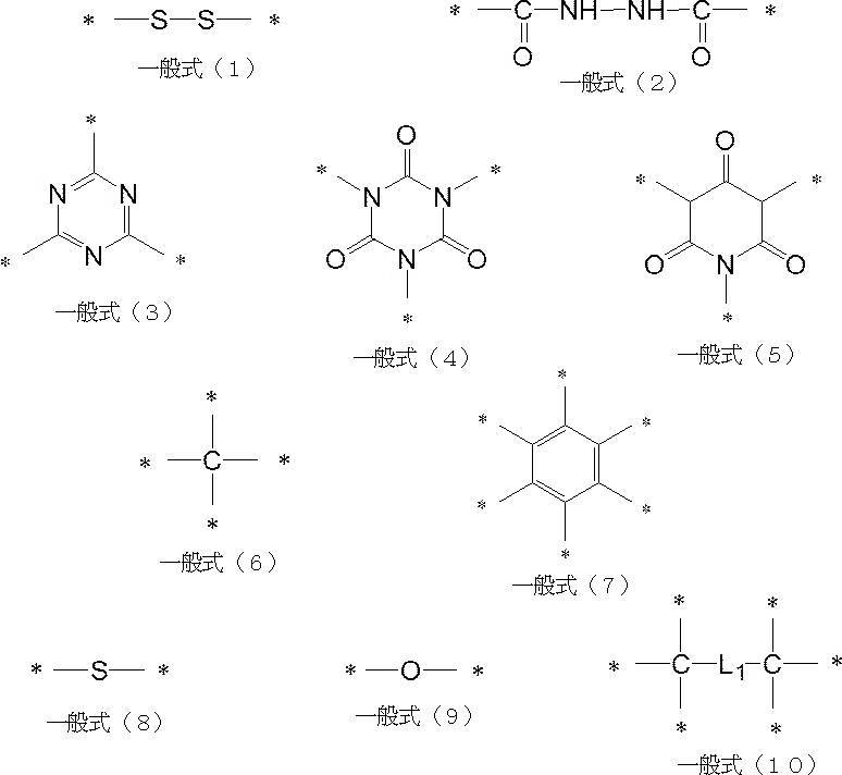
- 前記マイグレーション防止剤が前記化合物Xであり、
前記化合物X中に含まれる一般式(A)で表される基および一般式(B)で表される基の合計数が3以上である、請求項1または2に記載の有機半導体組成物。 The migration inhibitor is the compound X;
The organic-semiconductor composition of Claim 1 or 2 whose total number of group represented by general formula (A) and group represented by general formula (B) contained in the said compound X is 3 or more. - 請求項1~5のいずれか1項に記載の有機半導体組成物を使用して作製される有機半導体層。 An organic semiconductor layer produced using the organic semiconductor composition according to any one of claims 1 to 5.
- 請求項1~5のいずれか1項に記載の有機半導体組成物を使用して作製される有機半導体層と、ソース電極と、ドレイン電極と、ゲート電極とを含む有機薄膜トランジスタ。 An organic thin film transistor comprising an organic semiconductor layer produced using the organic semiconductor composition according to any one of claims 1 to 5, a source electrode, a drain electrode, and a gate electrode.
- 前記ソース電極、前記ドレイン電極、および、前記ゲート電極からなる群から選択される少なくとも1つが銀を含む、請求項7に記載の有機薄膜トランジスタ。 The organic thin film transistor according to claim 7, wherein at least one selected from the group consisting of the source electrode, the drain electrode, and the gate electrode contains silver.
- 請求項7または8に記載の有機薄膜トランジスタを含む電子ペーパー。 Electronic paper including the organic thin film transistor according to claim 7 or 8.
- 請求項7または8に記載の有機薄膜トランジスタを含むディスプレイデバイス。 A display device comprising the organic thin film transistor according to claim 7 or 8.
Priority Applications (4)
| Application Number | Priority Date | Filing Date | Title |
|---|---|---|---|
| JP2015529477A JPWO2015016003A1 (en) | 2013-07-31 | 2014-07-04 | Organic semiconductor composition, organic thin film transistor, electronic paper, display device |
| EP14831689.6A EP3029749B1 (en) | 2013-07-31 | 2014-07-04 | Organic semiconductor composition, organic thin film transistor, electronic paper and display device |
| CN201480038721.XA CN105359288B (en) | 2013-07-31 | 2014-07-04 | Organic semiconductor composition, OTFT, Electronic Paper and display device |
| US14/988,043 US10008682B2 (en) | 2013-07-31 | 2016-01-05 | Organic semiconductor composition, organic thin film transistor, electronic paper and display device |
Applications Claiming Priority (2)
| Application Number | Priority Date | Filing Date | Title |
|---|---|---|---|
| JP2013-158767 | 2013-07-31 | ||
| JP2013158767 | 2013-07-31 |
Related Child Applications (1)
| Application Number | Title | Priority Date | Filing Date |
|---|---|---|---|
| US14/988,043 Continuation US10008682B2 (en) | 2013-07-31 | 2016-01-05 | Organic semiconductor composition, organic thin film transistor, electronic paper and display device |
Publications (1)
| Publication Number | Publication Date |
|---|---|
| WO2015016003A1 true WO2015016003A1 (en) | 2015-02-05 |
Family
ID=52431543
Family Applications (1)
| Application Number | Title | Priority Date | Filing Date |
|---|---|---|---|
| PCT/JP2014/067906 WO2015016003A1 (en) | 2013-07-31 | 2014-07-04 | Organic semiconductor composition, organic thin film transistor, electronic paper and display device |
Country Status (5)
| Country | Link |
|---|---|
| US (1) | US10008682B2 (en) |
| EP (1) | EP3029749B1 (en) |
| JP (1) | JPWO2015016003A1 (en) |
| CN (1) | CN105359288B (en) |
| WO (1) | WO2015016003A1 (en) |
Cited By (1)
| Publication number | Priority date | Publication date | Assignee | Title |
|---|---|---|---|---|
| WO2016147773A1 (en) * | 2015-03-13 | 2016-09-22 | 富士フイルム株式会社 | Organic semiconductor film formation composition, organic thin film transistor, electronic paper, and display device |
Citations (8)
| Publication number | Priority date | Publication date | Assignee | Title |
|---|---|---|---|---|
| JP2005005582A (en) | 2003-06-13 | 2005-01-06 | Minolta Co Ltd | Organic semiconductor field-effect transistor |
| JP2005227441A (en) | 2004-02-12 | 2005-08-25 | Konica Minolta Medical & Graphic Inc | Photothermographic imaging material |
| JP2009507385A (en) * | 2005-09-05 | 2009-02-19 | オスラム オプト セミコンダクターズ ゲゼルシャフト ミット ベシュレンクテル ハフツング | Materials for n-type doping of electron transport layers in organic electronic devices |
| WO2010010791A1 (en) * | 2008-07-22 | 2010-01-28 | Dic株式会社 | Organic transistor and method for manufacturing the same |
| JP2011187868A (en) * | 2010-03-11 | 2011-09-22 | National Institute Of Advanced Industrial Science & Technology | Intermediate phase composition and organic semiconductor element using the same |
| WO2011157779A1 (en) * | 2010-06-18 | 2011-12-22 | Basf Se | Organic electronic devices comprising a layer of a pyridine compound and a 8-hydroxyquinolinolato earth alkaline metal, or alkali metal complex |
| WO2012112530A2 (en) * | 2011-02-14 | 2012-08-23 | E.I.Du Pont De Nemours And Company | Electroactive composition |
| WO2012118174A1 (en) * | 2011-03-02 | 2012-09-07 | 国立大学法人九州大学 | Organic field-effect transistor and organic semiconductor material |
Family Cites Families (5)
| Publication number | Priority date | Publication date | Assignee | Title |
|---|---|---|---|---|
| WO2000079617A1 (en) | 1999-06-21 | 2000-12-28 | Cambridge University Technical Services Limited | Aligned polymers for an organic tft |
| US20070051403A1 (en) * | 2005-09-02 | 2007-03-08 | Konica Minolta Business Technologies, Inc. | Photoelectric Converter and Dye Sensitized Solar Cell |
| CN103282421B (en) * | 2011-01-13 | 2015-05-27 | 巴斯夫欧洲公司 | Organic photovoltaic device and manufacturing method thereof |
| WO2013072853A1 (en) * | 2011-11-15 | 2013-05-23 | Basf Se | Organic semiconductor device and manufacturing method thereof |
| CN104919614A (en) * | 2012-10-11 | 2015-09-16 | 密歇根大学董事会 | Polymer photovoltaics employing a squaraine donor additive |
-
2014
- 2014-07-04 WO PCT/JP2014/067906 patent/WO2015016003A1/en active Application Filing
- 2014-07-04 CN CN201480038721.XA patent/CN105359288B/en not_active Expired - Fee Related
- 2014-07-04 EP EP14831689.6A patent/EP3029749B1/en active Active
- 2014-07-04 JP JP2015529477A patent/JPWO2015016003A1/en active Pending
-
2016
- 2016-01-05 US US14/988,043 patent/US10008682B2/en not_active Expired - Fee Related
Patent Citations (8)
| Publication number | Priority date | Publication date | Assignee | Title |
|---|---|---|---|---|
| JP2005005582A (en) | 2003-06-13 | 2005-01-06 | Minolta Co Ltd | Organic semiconductor field-effect transistor |
| JP2005227441A (en) | 2004-02-12 | 2005-08-25 | Konica Minolta Medical & Graphic Inc | Photothermographic imaging material |
| JP2009507385A (en) * | 2005-09-05 | 2009-02-19 | オスラム オプト セミコンダクターズ ゲゼルシャフト ミット ベシュレンクテル ハフツング | Materials for n-type doping of electron transport layers in organic electronic devices |
| WO2010010791A1 (en) * | 2008-07-22 | 2010-01-28 | Dic株式会社 | Organic transistor and method for manufacturing the same |
| JP2011187868A (en) * | 2010-03-11 | 2011-09-22 | National Institute Of Advanced Industrial Science & Technology | Intermediate phase composition and organic semiconductor element using the same |
| WO2011157779A1 (en) * | 2010-06-18 | 2011-12-22 | Basf Se | Organic electronic devices comprising a layer of a pyridine compound and a 8-hydroxyquinolinolato earth alkaline metal, or alkali metal complex |
| WO2012112530A2 (en) * | 2011-02-14 | 2012-08-23 | E.I.Du Pont De Nemours And Company | Electroactive composition |
| WO2012118174A1 (en) * | 2011-03-02 | 2012-09-07 | 国立大学法人九州大学 | Organic field-effect transistor and organic semiconductor material |
Non-Patent Citations (1)
| Title |
|---|
| See also references of EP3029749A4 |
Cited By (5)
| Publication number | Priority date | Publication date | Assignee | Title |
|---|---|---|---|---|
| WO2016147773A1 (en) * | 2015-03-13 | 2016-09-22 | 富士フイルム株式会社 | Organic semiconductor film formation composition, organic thin film transistor, electronic paper, and display device |
| US20170346018A1 (en) * | 2015-03-13 | 2017-11-30 | Fujifilm Corporation | Composition for forming organic semiconductor film, organic thin film transistor, electronic paper, and display device |
| JPWO2016147773A1 (en) * | 2015-03-13 | 2017-12-28 | 富士フイルム株式会社 | Composition for forming organic semiconductor film, organic thin film transistor, electronic paper, and display device |
| US10510965B2 (en) | 2015-03-13 | 2019-12-17 | Fujifilm Corporation | Composition for forming organic semiconductor film, organic thin film transistor, electronic paper, and display device |
| TWI688594B (en) * | 2015-03-13 | 2020-03-21 | 日商富士軟片股份有限公司 | Organic-semiconductor-film-forming composition, organic thin film transistor, electronic paper and display device |
Also Published As
| Publication number | Publication date |
|---|---|
| US10008682B2 (en) | 2018-06-26 |
| EP3029749A1 (en) | 2016-06-08 |
| CN105359288A (en) | 2016-02-24 |
| CN105359288B (en) | 2017-09-12 |
| JPWO2015016003A1 (en) | 2017-03-02 |
| US20160155964A1 (en) | 2016-06-02 |
| EP3029749B1 (en) | 2020-01-22 |
| EP3029749A4 (en) | 2016-08-31 |
Similar Documents
| Publication | Publication Date | Title |
|---|---|---|
| EP3007214B1 (en) | Composition for forming gate insulating film, organic thin film transistor, electronic paper, and display device | |
| US10510965B2 (en) | Composition for forming organic semiconductor film, organic thin film transistor, electronic paper, and display device | |
| US10138385B2 (en) | Conductive film forming composition, conductive film, organic thin film transistor, electronic paper, display device, and wiring board | |
| US9929348B2 (en) | Organic semiconductor composition comprising organic semiconductor material and polymer compound | |
| JP6143856B2 (en) | Organic semiconductor composition, organic thin film transistor, and electronic paper and display device | |
| JP6343678B2 (en) | Organic semiconductor composition, organic thin film transistor, electronic paper, display device | |
| WO2015016003A1 (en) | Organic semiconductor composition, organic thin film transistor, electronic paper and display device | |
| JP6259527B2 (en) | Organic electronic devices, organic thin film transistors, electronic paper, display devices | |
| WO2015046523A1 (en) | Organic semiconductor composition, organic thin film transistor, electronic paper and display device | |
| JP6043000B2 (en) | Composition for forming conductive film, conductive film, organic thin film transistor, electronic paper, display device and wiring board | |
| US20160230033A1 (en) | Conductive film forming composition, conductive film, organic thin film transistor, electronic paper, display device, and wiring board |
Legal Events
| Date | Code | Title | Description |
|---|---|---|---|
| WWE | Wipo information: entry into national phase |
Ref document number: 201480038721.X Country of ref document: CN |
|
| 121 | Ep: the epo has been informed by wipo that ep was designated in this application |
Ref document number: 14831689 Country of ref document: EP Kind code of ref document: A1 |
|
| ENP | Entry into the national phase |
Ref document number: 2015529477 Country of ref document: JP Kind code of ref document: A |
|
| WWE | Wipo information: entry into national phase |
Ref document number: 2014831689 Country of ref document: EP |
|
| NENP | Non-entry into the national phase |
Ref country code: DE |