WO2015015805A1 - 表示装置、パネルユニット及びバックライトユニット - Google Patents
表示装置、パネルユニット及びバックライトユニット Download PDFInfo
- Publication number
- WO2015015805A1 WO2015015805A1 PCT/JP2014/004008 JP2014004008W WO2015015805A1 WO 2015015805 A1 WO2015015805 A1 WO 2015015805A1 JP 2014004008 W JP2014004008 W JP 2014004008W WO 2015015805 A1 WO2015015805 A1 WO 2015015805A1
- Authority
- WO
- WIPO (PCT)
- Prior art keywords
- guide plate
- light guide
- led
- disposed
- light
- Prior art date
- Legal status (The legal status is an assumption and is not a legal conclusion. Google has not performed a legal analysis and makes no representation as to the accuracy of the status listed.)
- Ceased
Links
Images









Classifications
-
- G—PHYSICS
- G02—OPTICS
- G02B—OPTICAL ELEMENTS, SYSTEMS OR APPARATUS
- G02B6/00—Light guides; Structural details of arrangements comprising light guides and other optical elements, e.g. couplings
- G02B6/0001—Light guides; Structural details of arrangements comprising light guides and other optical elements, e.g. couplings specially adapted for lighting devices or systems
- G02B6/0011—Light guides; Structural details of arrangements comprising light guides and other optical elements, e.g. couplings specially adapted for lighting devices or systems the light guides being planar or of plate-like form
- G02B6/0066—Light guides; Structural details of arrangements comprising light guides and other optical elements, e.g. couplings specially adapted for lighting devices or systems the light guides being planar or of plate-like form characterised by the light source being coupled to the light guide
- G02B6/0073—Light emitting diode [LED]
-
- G—PHYSICS
- G02—OPTICS
- G02B—OPTICAL ELEMENTS, SYSTEMS OR APPARATUS
- G02B6/00—Light guides; Structural details of arrangements comprising light guides and other optical elements, e.g. couplings
- G02B6/0001—Light guides; Structural details of arrangements comprising light guides and other optical elements, e.g. couplings specially adapted for lighting devices or systems
- G02B6/0011—Light guides; Structural details of arrangements comprising light guides and other optical elements, e.g. couplings specially adapted for lighting devices or systems the light guides being planar or of plate-like form
- G02B6/0033—Means for improving the coupling-out of light from the light guide
- G02B6/005—Means for improving the coupling-out of light from the light guide provided by one optical element, or plurality thereof, placed on the light output side of the light guide
- G02B6/0055—Reflecting element, sheet or layer
-
- G—PHYSICS
- G02—OPTICS
- G02F—OPTICAL DEVICES OR ARRANGEMENTS FOR THE CONTROL OF LIGHT BY MODIFICATION OF THE OPTICAL PROPERTIES OF THE MEDIA OF THE ELEMENTS INVOLVED THEREIN; NON-LINEAR OPTICS; FREQUENCY-CHANGING OF LIGHT; OPTICAL LOGIC ELEMENTS; OPTICAL ANALOGUE/DIGITAL CONVERTERS
- G02F1/00—Devices or arrangements for the control of the intensity, colour, phase, polarisation or direction of light arriving from an independent light source, e.g. switching, gating or modulating; Non-linear optics
- G02F1/01—Devices or arrangements for the control of the intensity, colour, phase, polarisation or direction of light arriving from an independent light source, e.g. switching, gating or modulating; Non-linear optics for the control of the intensity, phase, polarisation or colour
- G02F1/13—Devices or arrangements for the control of the intensity, colour, phase, polarisation or direction of light arriving from an independent light source, e.g. switching, gating or modulating; Non-linear optics for the control of the intensity, phase, polarisation or colour based on liquid crystals, e.g. single liquid crystal display cells
- G02F1/133—Constructional arrangements; Operation of liquid crystal cells; Circuit arrangements
- G02F1/1333—Constructional arrangements; Manufacturing methods
- G02F1/1335—Structural association of cells with optical devices, e.g. polarisers or reflectors
- G02F1/1336—Illuminating devices
- G02F1/133624—Illuminating devices characterised by their spectral emissions
Definitions
- This disclosure relates to a display device, a panel unit, and a backlight unit.
- a so-called edge light type panel unit in which a diffusion sheet, a lens sheet, and a light guide plate are disposed on the back side of a liquid crystal panel and a light emitting diode (LED) is disposed as a backlight on the end surface of the light guide plate is known.
- LED light emitting diode
- An object of the present disclosure is to provide a display device, a panel unit, and a backlight unit that can achieve high luminance and power saving.
- a display device includes a display panel, a light guide plate that is disposed on a back side of the display panel, guides light to the display panel, and is disposed to face an end surface of the light guide plate, and has a blue wavelength band.
- a white LED module having a spectral peak in the green wavelength band; and a reflective sheet disposed on the back side of the light guide plate and reflecting light.
- the LED module preferably has a blue spectrum peak in a wavelength band of 420 nm to 460 nm and a green spectrum peak in a wavelength band of 500 nm to 600 nm.
- the LED module has a peak intensity Ib of a blue component and an intensity of a green component when the peak intensity of the spectrum in the blue wavelength band is Ib and the peak intensity of the spectrum in the green wavelength band is Ig.
- the ratio with respect to the peak intensity Ig is preferably 0.1 ⁇ Ig / Ib ⁇ 0.2.
- the LED module is disposed so as to face end faces at both ends in one direction of the light guide plate.
- a plurality of the LED modules are arranged to face the end face of the light guide plate, and the plurality of LED modules are spaced at an interval of 1.16 pieces / cm to 2.32 pieces / cm. Is preferably arranged.
- a plurality of the LED modules are mounted on one surface, and an LED bar disposed so that light emitted from the plurality of LED modules enters the light guide plate; and The other surface of the LED bar that contacts the heat radiating plate and / or the one surface of the heat radiating plate that contacts the LED bar.
- the surface roughness is preferably 10 ⁇ m to 25 ⁇ m in terms of centerline average roughness Ra.
- a plurality of the LED modules are mounted on one surface, and further includes an LED bar arranged so that light emitted from the plurality of LED modules is incident on the light guide plate,
- the LED bar is preferably made of a high thermal conductive insulating ceramic.
- a plurality of the LED modules are mounted on one surface, and an LED bar disposed so that light emitted from the plurality of LED modules enters the light guide plate; and
- a heat radiating plate arranged to be able to conduct heat with the other surface, a metal back bezel arranged to be able to conduct heat with the heat radiating plate and covering the back side of the light guide plate, and covering the light guide plate of the back bezel
- a working fluid is enclosed in a container having a flat shape, and a flat surface having a flat shape is provided in contact with the surface on the opposite side of the back bezel. It is preferable to further include a heat pipe.
- a display device is disposed on the back side of the liquid crystal panel, and a light guide plate that emits light incident from an end surface from one main surface and guides the light to the liquid crystal panel; and a longitudinal direction of the light guide plate
- a white LED module disposed opposite to the end faces of both ends and having a spectrum peak in a blue wavelength band and a green wavelength band, and interposed between the liquid crystal panel and the light guide plate, and the light guide plate
- a diffusion sheet that diffuses the light emitted from the liquid crystal panel, the lens sheet that is interposed between the liquid crystal panel and the light guide plate, and condenses the light emitted from the light guide plate; and the other main surface of the light guide plate And a reflection sheet that reflects light.
- the panel unit according to the present disclosure is disposed on the back side of the display panel, the light guide plate that guides light to the display panel, the light guide plate disposed to face the end surface of the light guide plate, and a blue wavelength band.
- a white LED module having a spectral peak in the green wavelength band; and a reflective sheet disposed on the back side of the light guide plate and reflecting light.
- a backlight unit is disposed on the back side of the display panel, and is disposed so as to face the end surface of the light guide plate that guides light to the display panel, and has a blue wavelength band and a green wavelength band.
- a white LED module having a spectral peak, and a reflective sheet that is disposed on the back side of the light guide plate and reflects light.
- the display device, the panel unit, and the backlight unit of the present disclosure it is possible to provide a display device, a panel unit, and a backlight unit that have high luminance and power saving by adopting the LED module as described above. It is suitable for signage because of its high brightness and power saving.
- FIG. 2 Front view of LED bar with LED module Sectional view along line BB in FIG.
- luminance The figure which shows the mounting pattern of LED of a present Example and a comparative example Table showing the relationship between luminance unevenness and luminance in Examples and Comparative Examples
- the figure explaining the measuring method of the temperature between LED modules A graph showing the relationship between the number of LED modules, brightness unevenness of panel
- FIG. 26 is a graph of FIG. Sectional drawing of the panel unit of 6th Embodiment The figure which shows the ratio of the contact area of the heat pipe and the back chassis The figure which shows the relationship between each comparative example and Example shown in FIG. 29, and the temperature fall rate of an LED module
- FIG. 1 is a front view of the panel unit of the first embodiment.
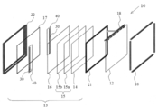
- FIG. 2 is an exploded perspective view of the panel unit according to the first embodiment.
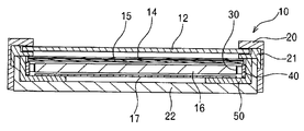
- FIG. 3 is a sectional view taken along line AA in FIG.
- the panel unit 10 includes a liquid crystal panel 12 and a backlight unit 13 disposed on the back side of the liquid crystal panel 12.
- the liquid crystal panel 12 is made of, for example, a front panel and a rear panel each having a transparent electrode, and a liquid crystal material (for example, VA or IPS system) disposed between the two panels.
- the front panel includes a first glass substrate, a color filter coated on the inner surface of the first glass substrate by being coated with an overcoat layer made of an acrylic resin or an epoxy resin, and a transparent electrode (for example, ITO (made of indium tin oxide), an alignment film formed on the transparent electrode, and a polarizing film (for example, a resin film such as polyethylene terephthalate) provided on the outer surface of the first glass substrate.
- the rear panel includes a second glass substrate and a switching element (for example, an amorphous Si thin film transistor (a-Si TFT) having a wiring material made of aluminum and a gate electrode (Cr)) formed on the inner surface of the second glass substrate.
- a switching element for example, an amorphous Si thin film transistor (a-Si TFT) having a wiring material made of aluminum and a gate electrode (Cr)
- the transparent electrode whose conduction / non-conduction is controlled by the switching element and the polarizing film provided on the outer surface of the second glass substrate.
- An alignment film is formed on the entire surface including the transparent electrode in the rear panel.
- the various members and liquid crystal materials constituting the liquid crystal panel 12 can be composed of known members and materials.
- a two-terminal element such as an MIM element, a varistor element, or a diode may be used as the switching element.
- the liquid crystal panel 12 is a 32-inch LCD panel, and has a horizontal (left / right) length of about 697.7 mm and a vertical (up / down) length of about 392.3 mm.
- the present disclosure is particularly preferably used for a panel unit including a large liquid crystal panel of 32 inches or more.
- the periphery of the liquid crystal panel 12 is held by an iron front bezel 20 and a plastic middle frame 21.
- the backlight unit 13 is configured by laminating a diffusion sheet 14, a lens sheet 15, and a light guide plate 16, and arranging a plurality of light emitting diodes (LEDs) 32 so as to face the left and right end faces of the light guide plate 16.
- LEDs light emitting diodes
- the diffusion sheet 14 is arranged on the back side of the liquid crystal panel 12 and is made of, for example, polyethylene terephthalate, and is arranged so that the peripheral edge abuts on the middle frame 21.
- the lens sheet 15 includes a Y-direction lens sheet 15 a and an X-direction lens sheet 15 b, is made of, for example, polyethylene terephthalate, and is disposed so as to overlap the back side of the diffusion sheet 14.
- the light guide plate 16 is made of, for example, polyethylene terephthalate, and is subjected to reflective dot printing or the like.
- the LED module 30 is disposed opposite to the left and right end faces of the light guide plate 16, and the reflective dot printing is formed to make the luminance of the entire screen uniform.
- the reflective dots are formed by, for example, an ink jet method, and dots having a diameter gradually increasing from the left and right end portions toward the central portion are formed.
- the dot system is formed with a minimum of 20 ⁇ m and a maximum of 50 ⁇ m, for example.
- the dot formation density and the dot shape are set as appropriate in order to make the luminance of the entire screen uniform.
- a reflection sheet 17 made of, for example, white polyethylene terephthalate is disposed on the back side of the light guide plate 16.
- Incident light from the LED module 30 disposed opposite to the left and right end surfaces of the light guide plate 16 is repeatedly reflected in the light guide plate 16, specifically between the reflective dots and the reflective sheet 17, and the surface side of the light guide plate 16. Emanates from.
- the light emitted from the light guide plate 16 becomes illumination light for the liquid crystal panel 12 via the lens sheet 15 and the diffusion sheet 14.
- a fine uneven shape such as a prism pattern or a dot pattern is formed in the light guide plate 16, and a process for efficiently guiding light incident in the light guide plate 16 toward the lens sheet 15 is performed.
- the light guide plate 16 is accommodated in a steel-made back bezel 22 having an open front surface, and the back bezel 22 is fitted to the front bezel 20 integrally with the LED module 30 and the like.
- the front bezel 20 has a horizontal (horizontal) length of 735.4 mm and a vertical (vertical) length of 433.0 mm.
- the thickness (length in the front-rear direction) when the back bezel 22 is fitted into the front bezel 20 is 10.8 mm at the minimum and 25.9 mm at the maximum.
- the LED module 30 serving as a backlight is disposed opposite to the left and right end faces of the light guide plate 16.
- the LED module 30 is disposed to face the end surface on the short side of the panel unit 10, but may be disposed to face the end surface on the long side (that is, the upper and lower end surfaces).
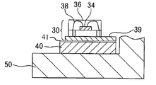
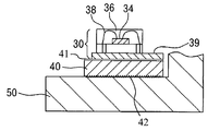
- the LED module 30 is formed by applying a phosphor 36 to the LED chip 34 and electrically connecting the electrode wires 38 to the wiring provided on the back side of the LED chip 34. Connected and configured.
- the LED chip 34 is a GaN blue LED having a peak wavelength of 460 nm.
- the phosphor 36 is a yellow fluorescent material (YAG).
- the electrode wire 38 is made of aluminum or gold, and the LED chip 34 is mounted on the LED bar 40 described later by a wire bonding method.
- the wiring pattern 39 is made of aluminum or copper, and the upper surface is coated with an insulating material.
- the LED module 30 of the present embodiment is packaged, and the package size is 2.0 mm short side, 4.0 mm long side, and 0.52 mm thickness.
- the luminous flux is 76 lm and the luminous intensity is 24.9 cd.
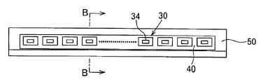
- the LED module 30 is arranged on the bowl-shaped LED bar 40 at a predetermined interval as shown in FIGS. 4 and 5.
- the long side of the LED bar 40 is substantially the same length as the short side of the light guide plate 16 and is made of a material excellent in heat conduction.
- the LED bar 40 of the present embodiment has a long side of about 400 mm, a short side of about 8 mm, and a thickness of 1 mm. 4 and 5, the LED bar 40 has a structure in which an insulating layer 41 made of a polyimide film is provided on the upper surface of an aluminum or copper plate, and a wiring pattern 39 is printed on the surface of the insulating layer 41.
- an insulating material may be used for the LED bar 40, and in that case, the insulating layer 41 may not be provided.
- the LED module 30 is disposed on one surface of the LED bar 40, and the other surface is in thermal contact with the heat sink 50.
- the heat sink 50 can employ aluminum, iron or the like. 3 to 4, the heat radiating plate 50 is substantially L-shaped, and the LED bar 40 is disposed inside the vertical side that is the front-rear direction when the panel unit 10 is viewed from the front side, and the rear side is inward. It extends.
- the heat sink 50 is attached to the back bezel 22 so that the LED module 30 can face inward and the end face of the light guide plate 16 can be irradiated.
- the heat radiating plate 50 is disposed such that the outer side surface is in thermal contact with the inner side surface of the back bezel 22 and the inner side surface is in thermal contact with the LED bar 40.
- the back bezel 22 accommodates the reflection sheet 17 and the light guide plate 16 and is housed in the front bezel 20.
- the image is formed by partially transmitting or blocking.
- the LED module 30 has a white ratio in which the ratio of the blue component Ib to the green component Ig is 0.1 ⁇ Ig / Ib ⁇ 0.2, preferably 0.12 ⁇ Ig / Ib ⁇ 0.17.
- the LED module 30 is used.
- FIG. 6 shows an emission spectrum of the white LED module 30.
- the wavelength peak of the blue component Ib may be 400 nm to 460 nm, and more preferably 440 nm to 460 nm.
- the wavelength peak of the green component Ig may be 500 nm to 600 nm, and more preferably 530 to 570 m. In FIG. 6, the wavelength peak of the blue component Ib is about 450 nm, and the wavelength peak of the green component Ig is about 550 nm.
- the efficiency of the white LED module 30 is determined by the efficiency of the blue LED that is the light source and the efficiency of the phosphor 36 that is the color conversion material.
- an LED used for a backlight of a liquid crystal panel often has an Ig / Ib of less than 0.1 or in a range of 0.4 or more in order to ensure luminance or consider color balance.
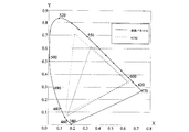
- FIG. 7 is a chromaticity diagram comparing the color reproduction range of the liquid crystal panel 12 using the LED module 30 of the present embodiment as a backlight and the color reproduction range according to the NTSC standard. Since the LED module 30 does not have a peak in the wavelength of the red component as shown in FIG. 6, the red reproducibility of the liquid crystal panel 12 is lower than that of the NTSC standard as shown in FIG.
- the light entering the eyes of an observer observing the liquid crystal panel 12 is light that has passed through the liquid crystal panel 12 and light that is reflected from the liquid crystal panel 12 by ambient light. Is the combined light. Accordingly, since the red component is supplemented by ambient light outdoors (particularly in the morning and evening), sufficient color reproducibility can be ensured.
- the LED module 30 with high luminous efficiency as a backlight, it is possible to realize high brightness and power saving of the liquid crystal panel 12, and ensure sufficient color reproducibility especially when used outdoors. can do.
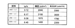
- FIG. 8 shows the characteristics of the LED module 30 (Sample 1 and Sample 2) of the example and the LED module (Sample 3 and Sample 4) of the comparative example as a single unit and the characteristics in a state in which they are incorporated in the panel unit 10. It is a table. The characteristics in the incorporated state are the measurement results when the drive current is 100 mA and the all white 100% pattern is displayed. In the figure, x and y indicate the chromaticity in the chromaticity diagram.
- the ratio of the blue component Ib and the green component Ig is in the range of 0.1 ⁇ Ig / Ib ⁇ 0.2.
- the color temperature in the assembled state is lower than that of the sample 3, but a higher color temperature than that of the sample 4 can be realized, and it can be seen that the color reproducibility is good.
- the luminance is higher than that of the comparative examples (Sample 3 and Sample 4), and it can be seen that high luminance can be achieved.
- FIG. 9 is a table showing the luminance and luminous efficiency in the state in which the LED modules of the example and the comparative example are incorporated in the panel unit 10.
- the panel unit 10 employing the LED module 30 of the example can achieve higher luminance and higher luminous efficiency than the comparative example.
- the luminous efficiency is compared by the surface luminance per 1 W (cd / m 2 ).
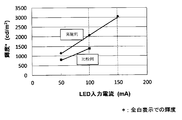
- FIG. 10 is a graph showing the relationship between the drive current and the luminance in the state in which the LED modules of the example (sample 2) and the comparative example (sample 4) are incorporated in the panel unit 10.
- the embodiment can obtain a higher luminance (cd / m 2 ) for the same input current (mA) than the comparative example, in other words, to obtain the same luminance. It can be seen that a small current value is sufficient.
- the use of the LED module 30 in which the ratio of the blue component Ib and the green component Ig is 0.1 ⁇ Ig / Ib ⁇ 0.2 enables a high-luminance panel.
- Unit 10 can be provided. Further, since the light emission efficiency of the LED module 30 is high, it is also effective for power saving of the panel unit 10. Further, high luminance can be realized with high efficiency with respect to the drive current.
- the panel unit For a conventional panel unit, high brightness and low power consumption of the panel unit can be achieved simply by replacing the light source with the LED module 30.
- the LED module 30 can be manufactured at a relatively low cost, and the price of the panel unit can be reduced.
- an edge light type panel unit 10 having a luminance of 3000 cd / m 2 or more can be realized.
- the display device incorporating the panel unit 10 is also suitable for signage requiring long-time lighting.
- the panel unit and the display device including the panel unit are arranged on the liquid crystal panel 12, the back side of the liquid crystal panel 12, the light guide plate 16 that guides light to the liquid crystal panel 12, and the end face of the light guide plate 16.
- a white LED module 30 that is disposed opposite to each other and has a spectrum peak in a blue wavelength band and a green wavelength band, and a reflection sheet 17 that is disposed on the back side of the light guide plate 16 and reflects light.
- the backlight is disposed on the back side of the liquid crystal panel 12, and is disposed opposite to the light guide plate 16 that guides light to the liquid crystal panel 12, and the end surface of the light guide plate 16, and has a blue wavelength band and a green wavelength band.
- the LED module 30 has a blue spectrum peak in a wavelength band of 420 nm or more and 460 nm or less, and a green spectrum peak in a wavelength band of 500 nm or more and 600 nm or less. Thereby, light in a wavelength band of 420 nm or more and 460 nm or less and light in a wavelength band of 500 nm or more and 600 nm or less are combined, and white light with high luminance and power saving can be realized.
- the LED module 30 has a peak intensity Ib of the spectrum in the blue wavelength band and Ig peak intensity of the spectrum in the green wavelength band, and the peak intensity Ib of the blue component and the peak intensity Ig of the green component
- the ratio is 0.1 ⁇ Ig / Ib ⁇ 0.2.
- the LED module 30 is disposed so as to face the end faces at both ends in one direction (longitudinal direction) of the light guide plate 16.
- an edge light type panel unit suitable for signage is formed.
- the LED modules 30 are arranged on the LED bar 40 at a predetermined interval.
- the present embodiment relates to the arrangement of the LED module 30 in the LED bar 40.
- the luminance and the uniformity of the display surface can be improved by increasing the number of LED modules to be mounted.
- the number of LED modules increases, power consumption, heat generation amount, or cost will increase.
- the arrangement interval of the LED modules 30 in the LED bar 40 will be described in detail, in which the luminance unevenness is kept within an allowable range while maintaining a certain luminance while reducing the number of LED modules.
- FIG. 11 is a diagram showing a mounting pattern of the LED module.
- the LED module 30 has a short direction (short side of the package of the LED module 30) and a long direction of the LED bar 40 (long side of the LED bar 40) in parallel.
- the LED modules 30 are arranged with an interval of 0.3 mm on the mounting structure.
- Patterns 1 to 3 are examples, and patterns 4 to 6 are comparative examples for comparison.
- the white (white) portion indicates the LED module 30 that is lit, and the black portion indicates the LED module 30 that is not lit.
- pattern 1 turns on all LED modules 30.
- Pattern 2 is a repetition of a pattern in which two LED modules 30 are lit and one LED module 30 is not lit.
- Pattern 3 repeats lighting / non-lighting of the LED modules 30 one by one.
- Pattern 4 is a repetition of a pattern in which one LED module 30 is lit and three LED modules 30 are not lit.
- the pattern 5 turns on one LED module 30 and does not turn on the five LED modules 30, and the pattern 6 repeats a pattern that turns on one LED module 30 and does not turn on the seven LED modules 30. It is.
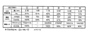
- the arrangement of the LED modules 30 in each pattern is 2.32 / cm for pattern 1, 1.55 / cm for pattern 2, and 1.16 for pattern 3.
- Pieces / cm, the pattern 4 as a comparative example is 0.58 pieces / cm, the pattern 5 is 0.39 pieces / cm, and the pattern 6 is 0.29 pieces / cm.
- the mounting density of the LED modules 30 is a percentage display of the sum of the occupied lengths of the LED modules 30 in the length of the LED bars 40.
- the intervals are not portions occupied by the LED modules 30. Therefore, for example, in the pattern 1, the length obtained by reducing the interval between the LED modules 30 indicated by the length of the LED bar 40 is the sum of the occupied lengths of the LED modules 30 in the length of the LED bars 40. Further, if the luminance unevenness of the pattern 1 and the pattern 3 is 100%, the luminance unevenness of the pattern 2 is also 100%, so the luminance unevenness of the pattern 2 in FIG. 12 is not measured.
- the luminance unevenness measurement performed in the present embodiment is measured under conditions (strict conditions) that are easily determined as luminance unevenness as compared with general luminance unevenness measurement.
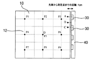
- general luminance unevenness measurement for example, the luminance is measured by comparing the luminance at the center point (points P1 to P9 shown in FIG. 13) of each region obtained by dividing the liquid crystal panel into nine parts.
- the luminance unevenness measurement of this embodiment measures and compares the luminance at a position 1 cm vertically away from the LED module 30, and the above-described general luminance unevenness may be determined as luminance unevenness. Increased compared to measurement.
- the brightness of each pattern is smaller than that of the pattern 1 as an example.
- the luminance of the LED modules 30 can be increased by passing a large operating current through the LED modules 30.
- the amount of heat generated by each LED module 30 increases as the operating current increases, the thermal influence of one LED module 30 on another LED module 30 can be suppressed due to the sparse arrangement. Therefore, the brightness of pattern 2 and pattern 3 is lower than that of pattern 1, but by increasing the operating current, it is possible to suppress the decrease in brightness, and it can withstand practical use sufficiently.
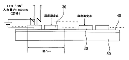
- the temperature between the LED modules 30 was measured for heat conduction between the LED modules 30. As shown in FIG. 15, the temperature was measured by measuring the wavelength of the LED at a certain distance from the emitting LED and measuring the relationship between the LED mounting density and the temperature change.
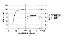
- the mounting density of the LED modules 30 is preferably 2.32 pieces / cm or less in order to suppress the influence of heat between the LEDs.
- the optimal LED module 30 mounting density is 1.16 pieces / cm to 2.32 pieces / cm.
- a plurality of LED modules 30 are arranged facing the end face of the light guide plate 16, and the plurality of LED modules are arranged at intervals of 30, 1.16 pieces / cm to 2.32 pieces / cm.
- the mounting density of the LED modules 30 is optimized, and a panel unit with high luminance and power saving can be provided without impairing the uniformity of the screen.
- the panel unit 10 can be made uniform and the cost can be reduced.
- the cooling means of the LED module 30 can be configured simply, and the panel unit 10 can be made thinner and lighter.
- the LED module 30 generates heat with light emission, and efficiently dissipates the generated heat. There is a need. This is because when the heat radiation is not performed efficiently, the temperature of the LED module 30 rises, the reliability of the LED module 30 is lowered, and the light emission efficiency may be lowered. Therefore, in this embodiment, the heat dissipation efficiency of the LED module 30 is increased, and further high reliability is achieved.
- the LED modules 30 are arranged on the LED bar 40 at predetermined intervals.
- the LED module 30 is disposed on one surface of the LED bar 40, and the other surface of the LED bar 40 is in thermal contact with the heat sink 50.
- it is necessary to lower the thermal efficiency in the process from the LED module 30 to the heat radiating plate 50.
- the thermal resistance that exists in the process from the LED module 30 to the heat sink 50 is the thermal resistance of each member.
- the thermal resistance of the LED chip 34, the thermal resistance of the wiring pattern 39, the thermal resistance of the insulating layer 41, the LED bar 40 and the heat resistance of the heat sink 50 see FIG. 5.
- it is difficult to reduce the thermal resistance of each member unless the material is changed it is necessary to increase the heat transfer efficiency between the members in order to reduce the overall thermal resistance when the material is not changed.
- unevenness 42 is formed on the other surface of the LED bar 40 that contacts the heat sink 50.
- the unevenness 42 formed on the LED bar 40 preferably has a center line average roughness Ra of 10 ⁇ m to 25 ⁇ m.
- the unevenness 42 of the LED bar 40 can be formed, for example, by fabricating the LED bar 40 by sintering and not subjecting the surface of the fabricated LED bar 40 that contacts the heat sink 50 to mechanical processing such as polishing.
- corrugation 42 can also be formed by giving rough surface processing to the LED bar 40, or giving blasting and sputtering.
- the LED bar 40 is connected to the heat radiating plate 50 with solder (for example, Sn—Pb, Sn—Ag—Cu, Sn—Zn—Al, Sn—Bi—Ag solder having high thermal conductivity) or heat conduction. It is fixed so as to be in thermal contact with an adhesive having excellent properties and a polymer tape having excellent thermal conductivity.
- solder for example, Sn—Pb, Sn—Ag—Cu, Sn—Zn—Al, Sn—Bi—Ag solder having high thermal conductivity
- the heat transfer efficiency from the LED bar 40 to the heat radiating plate 50 is increased by the thermal contact between the LED bar 40 and the heat radiating plate 50 with the surface area increased due to the formation of the unevenness 42 by tin-based solder. Thereby, the temperature rise of the LED module 30 can be reduced as much as possible. Further, by forming the irregularities 42, the adhesive strength between the LED bar 40 and the heat sink 50 can be improved.
- the heat radiating plate 50 is attached to the back bezel 22 so that the LED module 30 faces inward and the end face of the light guide plate 16 can be irradiated.
- the heat radiating plate 50 is disposed such that the outer side surface is in thermal contact with the inner side surface of the back bezel 22 and the inner side surface is in thermal contact with the LED bar 40.
- the back bezel 22 accommodates the reflection sheet 17 and the light guide plate 16 and is fitted to the front bezel 20.
- the surface roughness (Ra) of the LED bar 40 is (A) 5 ⁇ m, (B) 10 ⁇ m, (C) 15 ⁇ m, (D) 20 ⁇ m, (E) 25 ⁇ m, and the heat sink 50 And were attached so as to be in thermal contact with solder.
- the interface surface area between the LED bar 40 and the heat sink 50 is 100 ⁇ m 2 .
- the interface surface area between the LED bar 40 and the heat sink 50 is 220 ⁇ m 2 .
- the interface surface area between the LED bar 40 and the heat sink 50 is 510 ⁇ m 2 . Therefore, as can be seen by comparing the interfacial surface areas of (A) and (B), by setting the surface roughness (Ra) to 10 ⁇ m to 25 ⁇ m, when uneven processing is not performed (that is, the surface roughness (Ra) is 5 ⁇ m). It can be seen that the interface surface area with the heat sink 50 can be doubled or more as compared to the following case).
- the unevenness 42 is formed on the other surface of the LED bar 40 (surface that contacts the heat sink 50), but on one surface of the heat sink 50 (surface that contacts the LED bar 40). It is good also as forming, and it is good also as forming in both the LED bar 40 and the heat sink 50.
- the same effects as those of the first embodiment and the second embodiment are obtained.
- the surface roughness of the other surface of the LED bar 40 in contact with the heat sink 50 and / or one surface of the heat sink 50 in contact with the LED bar 40 is 10 ⁇ m to 25 ⁇ m in terms of the center line average roughness Ra. .
- the heat dissipation efficiency from the LED bar 40 to the heat sink 50 is increased by increasing the surface area of the contact interface between the LED bar 40 and the heat sink 50.
- the method for increasing the heat radiation efficiency of the LED module 30 is not limited to this, and as described in the third embodiment, the material of the member may be optimized.
- the LED bar 40 has a structure in which an insulating layer 41 made of a polyimide film is provided on the upper surface of an aluminum or copper plate.
- the LED bar 40 has a high thermal conductive insulating property such as aluminum nitride. Consists of ceramics.
- the LED bar 40 has high thermal conductivity and is formed of ceramics which is an insulating material, it is not necessary to provide an insulating layer between the LED module 30 and the LED bar 40, and the LED module 30 is directly applied. It can be arranged to touch. Therefore, the heat dissipation efficiency from the LED module 30 to the LED bar 40 can be increased.
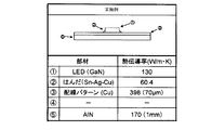
- FIG. 18 is a diagram showing the thermal conductivity of each member in the present embodiment in which aluminum nitride is adopted as the high thermal conductive insulating ceramic for the LED bar 40.
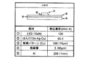
- FIG. 19 is a diagram showing the thermal conductivity of each member in a comparative example in which conductive aluminum having excellent thermal conductivity is adopted for the LED bar 40 and an insulating layer 41 is formed between the LED bar 40 and the LED module 30. It is.
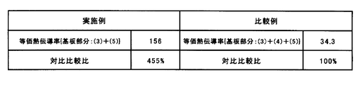
- FIG. 20 is a diagram showing the equivalent thermal conductivity of the substrate portions of this embodiment and the comparative example.
- the insulating layer 41 is provided in the comparative example, and the insulating layer is not provided in the present embodiment. Therefore, it is clear that the present embodiment having no insulating layer has a lower equivalent thermal conductivity than the comparative example having an insulating layer.
- the thermal conductivity of the LED bar 40 made of aluminum is lower than that of the LED bar 40 made of aluminum nitride. This also clearly shows that the present embodiment has a lower equivalent thermal conductivity than the comparative example.
- equivalent thermal conductivity the wiring pattern 39, an insulating layer (only a comparative example), the synthetic thermal conductivity of the LED bar 40) of the board
- Equivalent thermal conductivity (synthesis part) total thickness of printed wiring board ((3) + (4) + (5) in FIGS. 17 and 18) / ⁇ ⁇ i layer thickness / (i layer heat) Conductivity ⁇ i-layer wiring pattern remaining rate) ⁇
- i layer is (3) or (4) or (5).
- the wiring pattern remaining rate was set to 1 for the (4) and (5) layers and 0.18 for the (3) layer.
- the equivalent thermal conductivity of the substrate portion of the present embodiment is calculated by the mathematical formula shown in FIG. 21A, and the equivalent thermal conductivity of the substrate portion of the comparative example is given by the mathematical formula shown in FIG. Calculated.
- the temperature rise by the insulating layer 41 interposing can be calculated by the following.
- the area A of the LED chip 34 is 0.5 mm 2 (0.5 mm ⁇ 0.5 mm ⁇ 2), the size contribution ratio s of the insulating layer is 100%, the thickness t of the insulating layer is 80 ⁇ m, and the thermal conductivity of the insulating layer
- ⁇ is 3 W / m ⁇ K
- a temperature rise can be suppressed to 1/5 compared with a comparative example.
- the same effects as those of the first embodiment and the second embodiment are obtained.
- the thermal conductivity is increased as compared with other members (aluminum and copper), and the heat generated from the LED module 30 is efficiently radiated. be able to. Therefore, it becomes possible to flow a large current to the LED module 30, and it is possible to achieve high brightness and high reliability of the backlight unit 11, the panel unit 10 including the backlight unit 11, and the display device on which the panel unit 10 is mounted. it can.
- heat generated in the LED module 30 is efficiently transferred to the heat radiating plate 50 and further transferred to the back bezel 22, thereby increasing the heat dissipation efficiency of the LED module 30. . Furthermore, in order to improve the heat dissipation efficiency of the LED module 30, it is desirable to transfer the heat transmitted to the back bezel 22 to another member.
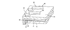
- the heat pipe 60 is disposed on the back side of the back bezel 22.
- the heat pipe 60 is arranged such that one end (high temperature portion) is in thermal contact with the back bezel 22 and the free end side (cooling portion) is not in contact with the back bezel 22.
- the heat pipe 60 is installed inward from the short side edge of the back bezel 22 so that one end of the heat pipe 60 faces the heat sink 50 with the back bezel 22 in between.
- the heat pipe 60 is disposed so as to be inclined obliquely upward from the high temperature portion in thermal contact with the back bezel 22 toward the cooling portion on the free end side. Is preferred.
- the heat pipe 60 can be configured by enclosing a working fluid inside a container 62.
- a working fluid an aqueous acetone solution can be exemplified.
- the container 62 has a flat shape, and the flat surface is in thermal contact with the back bezel 22 in a wide area.
- the heat pipe 60 is slightly bent so that the cooling portion on the free end side that does not come into contact with the back bezel 22 is separated from the back bezel 22.
- FIG. 25 is a table showing the relationship between the number of installed heat pipes 60, the junction temperature of the LED module 30, and the luminance.
- the number of the heat pipes 60 is six.
- the junction temperature is the temperature of the highest part of the pn junction.
- the junction temperature of the LED module 30 can be lowered by increasing the number of installed heat pipes 60. Moreover, it turns out that the brightness
- FIG. 25 it can be seen that the junction temperature of the LED module 30 can be lowered by increasing the number of installed heat pipes 60. Moreover, it turns out that the brightness
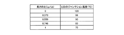
- FIGS. 26 and 27 are tables showing changes in the junction temperature of the LED module 30 when the ratio of the short side length Lb of the back bezel 22 to the total length Lp of the short side of the heat pipe 60 is changed. It is the graph which illustrated the result.
- the junction temperature of the LED module 30 decreases as Lp / Lb increases, that is, the total length on the short side of the heat pipe 60 increases.
- Lp / Lb is about 0.6 or more
- the junction temperature can be lowered by 30 ° C. or more. Since the heat generation of the LED module 30 is suppressed, the luminance of the LED module 30 can be increased.
- the same effects as those of the third embodiment and the fourth embodiment are obtained.
- the heat pipe 60 is disposed on the back bezel 22, the heat of the back bezel 22 is transmitted to the container 62.
- the working fluid absorbs heat inside the high temperature part and evaporates, and moves to the cooling part through the container 62.
- the working fluid that has moved to the cooling section is cooled and agglomerated, becomes liquid again, and returns to the high temperature section.
- the working fluid circulates in the container 62, whereby the heat absorption from the back bezel 22 can be efficiently performed, and the heat dissipation efficiency of the LED module 30 can be improved.
- the heat transfer efficiency of the LED module 30 is increased by transferring the heat transferred to the back bezel 22 to the heat pipe 60.
- the heat transferred to the heat pipe 60 is further transferred to another member.
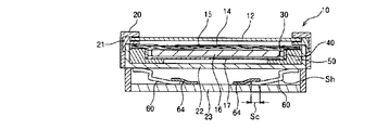
- the back side of the back bezel 22 is covered with the back chassis 23.
- the back bezel 22 and the back chassis 23 are thermally connected by the heat pipe 60.
- the heat pipe 60 is disposed such that one end (high temperature portion) faces the heat radiating plate 50 with the back bezel 22 interposed therebetween, and is in thermal contact with the heat radiating plate 50, and the other end (cooling portion) is the back. Arranged to be in thermal contact with the chassis 23.
- a plurality of heat pipes 60 can be arranged (see FIGS. 22 to 24).
- the heat pipe 60 connects the heat sink 50 and the back chassis 23 with high heat exchange efficiency with the back bezel 22 interposed therebetween.
- the heat pipe 60 is arranged so that 8 to 18% of the total surface area of the container 62 is in contact with the back chassis 23.
- the heat pipe 60 has a flat container 62, and the flat surface is in thermal contact with the back bezel 22 and the back chassis 23 over a wide area.
- the heat pipe 60 is bent slightly so that a step is generated between the cooling part and the high temperature part in order to take a large contact area between the back bezel 22 and the back chassis 23.
- the heat pipe 60 can be attached to the back bezel 22 and the back chassis 23 by adhesion or soldering with a high thermal conductive resin, or as shown in FIG.
- FIG. 29 is a diagram showing the ratio of the contact area between the heat pipe 60 and the back chassis 23, and FIG. 30 shows the relationship between each comparative example and example shown in FIG. 29 and the temperature decrease rate of the LED module 30.
- the heat radiation area is constant (83 cm 2 )
- the contact area Sc indicates the area of the part where the heat pipe 60 and the back chassis 23 are in contact as shown in FIG.
- the example in FIG. 29 is an example to which the structure of the present disclosure is applied, and the comparative example is an example produced for comparison.
- the comparative example 1 is an Example in which the heat pipe 60 is not attached.
- the same effect as that of the fifth embodiment is obtained.
- the heat of the back bezel 22 is transferred to the back chassis 23 via the container 62. Is transmitted to. Therefore, the heat dissipation efficiency of the LED module 30 can be further increased.
- Embodiments 1 to 6 have been described as examples of the technology disclosed in the present application. However, the technology in the present disclosure is not limited to this, and can also be applied to embodiments that have been changed, replaced, added, omitted, and the like. Also, it is possible to combine the components described in the first to sixth embodiments to form a new embodiment.
- the configuration and structure of the liquid crystal panel 12, the diffusion sheet 14, the lens sheet 15, and the light guide plate 16, the configuration of the LED bar 40, and the like are not limited to the above.
- the back bezel 22 is provided between the heat pipe 60 and the heat radiating plate 50, but the back bezel 22 may be omitted and the heat pipe 60 may be disposed so as to be in direct contact with the heat radiating plate 50. Good.
- the edge light type panel unit is used as the panel unit, but it may be a direct light type panel unit.
- the present disclosure can be used for display devices, panel units, and backlight units.
Landscapes
- Physics & Mathematics (AREA)
- General Physics & Mathematics (AREA)
- Optics & Photonics (AREA)
- Engineering & Computer Science (AREA)
- Microelectronics & Electronic Packaging (AREA)
- Planar Illumination Modules (AREA)
- Liquid Crystal (AREA)
Abstract
表示パネルと、前記表示パネルの背面側に配置され、前記表示パネルへ光を導く導光板と、前記導光板の端面に対向して配置され、青色の波長帯域と緑色の波長帯域とにスペクトルのピークを有する白色のLEDモジュールと、前記導光板の背面側に配置され、光を反射する反射シートと、を有する。
Description
本開示は表示装置、パネルユニット及びバックライトユニットに関する。
表示装置のパネルユニットとして、液晶パネルの背面側に拡散シート、レンズシート及び導光板を配設し、導光板の端面にバックライトとして発光ダイオード(LED)を配置した所謂エッジライト型パネルユニットが知られている(たとえば、特許文献1参照)。
液晶表示装置では、液晶パネルの色再現性を重視するために、LEDの効率を犠牲にしていたことから、高輝度且つ省電力のパネルユニットを実現することは困難であった。
サイネージ用に用いられる液晶表示装置の場合、明るい屋外での使用に際し、屋内用に比して高輝度、より具体的には1500cd/m2を越えるような高輝度のパネルユニットが求められている。
本開示の目的は、高輝度且つ省電力を達成することのできる表示装置、パネルユニット及びバックライトユニットを提供することである。
本開示に係る表示装置は、表示パネルと、前記表示パネルの背面側に配置され、前記表示パネルへ光を導く導光板と、前記導光板の端面に対向して配置され、青色の波長帯域と緑色の波長帯域とにスペクトルのピークを有する白色のLEDモジュールと、前記導光板の背面側に配置され、光を反射する反射シートと、を有する。
上記構成の表示装置において、前記LEDモジュールは、420nm以上460nm以下の波長帯域に青色のスペクトルのピークを有しており、500nm以上600nm以下の波長帯域に緑色のスペクトルのピークを有することが好ましい。
上記構成の表示装置において、前記LEDモジュールは、青色の波長帯域におけるスペクトルのピーク強度をIbとし、緑色の波長帯域におけるスペクトルのピーク強度をIgとするとき、青色成分のピーク強度Ibと緑色成分のピーク強度Igのとの比が0.1≦Ig/Ib≦0.2であることが好ましい。
上記構成の表示装置において、前記LEDモジュールは、前記導光板の一方向の両端の端面に対向して配置されることが好ましい。
上記構成の表示装置において、前記LEDモジュールは、前記導光板の端面に対向して複数個配置されており、複数個のLEDモジュールは、1.16個/cm~2.32個/cmの間隔で配置されることが好ましい。
上記構成の表示装置において、複数個の前記LEDモジュールを一方の面に搭載し、前記複数個のLEDモジュールから出射する光が前記導光板に入射するよう配置されたLEDバーと、前記LEDバーの他方の面と熱伝導可能に配置される放熱板と、をさらに有し、前記放熱板に当接する前記LEDバーの他方の面および/または前記LEDバーに当接する前記放熱板の一方の面の表面粗さは、中心線平均粗さRaで10μm~25μmであることが好ましい。
上記構成の表示装置において、複数個の前記LEDモジュールを一方の面に搭載し、前記複数個のLEDモジュールから出射する光が前記導光板に入射するよう配置されたLEDバーをさらに有し、前記LEDバーは、高熱伝導絶縁性セラミックスから構成されることが好ましい。
上記構成の表示装置において、複数個の前記LEDモジュールを一方の面に搭載し、前記複数個のLEDモジュールから出射する光が前記導光板に入射するよう配置されたLEDバーと、前記LEDバーの他方の面と熱伝導可能に配置される放熱板と、前記放熱板と熱伝導可能に配置され、前記導光板の背面側を覆う金属製のバックベゼルと、前記バックベゼルの前記導光板を覆う側とは反対側の面に配置され、扁平形状を有するコンテナの内部に作動流体が封入され、扁平形状の平坦な面が前記バックベゼルの前記反対側の面と接触するように設けられる複数のヒートパイプと、をさらに有することが好ましい。
本開示に係る表示装置は、前記液晶パネルの背面側に配置され、端面から入射した光を一方の主面から出射して前記液晶パネルへ光を導く導光板と、前記導光板の長手方向の両端の端面に対向して配置され、青色の波長帯域と緑色の波長帯域とにスペクトルのピークを有する白色のLEDモジュールと、前記液晶パネルと前記導光板との間に間挿され、前記導光板から出射した光を拡散させる拡散シートと、前記液晶パネルと前記導光板との間に間挿され、前記導光板から出射した光を集光するレンズシートと、前記導光板の他方の主面に配置され、光を反射する反射シートと、を有する。
本開示に係るパネルユニットは、表示パネルと、前記表示パネルの背面側に配置され、前記表示パネルへ光を導く導光板と、前記導光板の端面に対向して配置され、青色の波長帯域と緑色の波長帯域とにスペクトルのピークを有する白色のLEDモジュールと、前記導光板の背面側に配置され、光を反射する反射シートと、を有する。
本開示に係るバックライトユニットは、表示パネルの背面側に配置され、前記表示パネルへ光を導く導光板と、前記導光板の端面に対向して配置され、青色の波長帯域と緑色の波長帯域とにスペクトルのピークを有する白色のLEDモジュールと、前記導光板の背面側に配置され、光を反射する反射シートと、を有する。
本開示の表示装置、パネルユニット及びバックライトユニットによれば、上記の如きLEDモジュールを採用することにより、高輝度且つ省電力な表示装置、パネルユニット及びバックライトユニットを提供できる。高輝度且つ省電力であるため、サイネージ用としても好適である。
以下、適宜図面を参照しながら、実施の形態を詳細に説明する。但し、必要以上に詳細な説明は省略する場合がある。例えば、既によく知られた事項の詳細説明や実質的に同一の構成に対する重複説明を省略する場合がある。これは、以下の説明が不必要に冗長になるのを避け、当業者の理解を容易にするためである。なお、添付図面および以下の説明は、当業者が本開示を十分に理解するために、提供されるのであって、これらにより特許請求の範囲に記載の主題を限定することは意図されていない。
<第1実施形態>
以下、第1実施形態に係るパネルユニット10について、図面を参照しながら詳説する。図1は第1実施形態のパネルユニットの正面図である。図2は第1実施形態のパネルユニットの分解斜視図である。図3は図1の線A-Aに沿う断面図である。
<第1実施形態>
以下、第1実施形態に係るパネルユニット10について、図面を参照しながら詳説する。図1は第1実施形態のパネルユニットの正面図である。図2は第1実施形態のパネルユニットの分解斜視図である。図3は図1の線A-Aに沿う断面図である。
パネルユニット10は液晶パネル12及び液晶パネル12の背面側に配されるバックライトユニット13を備える。
液晶パネル12は、たとえば、共に透明電極を備えたフロントパネル及びリアパネルと、両パネルの間に配置された液晶材料(例えばVAやIPS系)から成る。フロントパネルは、第1ガラス基板と、アクリル系樹脂やエポキシ系樹脂から成るオーバーコート層によって被膜されて第1ガラス基板の内面に設けられるカラーフィルタと、オーバーコート層上に設けられる透明電極(例えばITO(インジウム錫酸化物)から成る)と、透明電極上に形成される配向膜と、第1ガラス基板の外面に設けられた偏光フィルム(例えばポリエチレンテレフタレートなどの樹脂フィルム)とから構成される。
リアパネルは、第2ガラス基板と、第2ガラス基板の内面に形成されたスイッチング素子(例えば、アルミニウムから成る配線材料とゲート電極(Cr)とを有する非晶質Si薄膜トランジスタ(a-SiTFT))と、スイッチング素子によって導通/非導通が制御される透明電極と、第2ガラス基板の外面に設けられた偏光フィルムとから構成される。リアパネルにおいて透明電極を含む全面には配向膜が形成される。
なお、液晶パネル12を構成する各種の部材や液晶材料 は、周知の部材、材料から構成することができる。また、スイッチング素子として、3端子素子である薄膜トランジスタ以外に、MIM素子、バリスタ素子、ダイオード等の2端子素子を用いてもよい。
本実施形態において液晶パネル12は32インチのLCDパネルであり、水平方向(左右方向)の長さが約697.7mm、垂直方向(上下方向)の長さが約392.3mmである。本開示は特に、32インチ以上の大型の液晶パネルを備えるパネルユニットに好適に使用される。
液晶パネル12の周囲は、鉄製のフロントベゼル20とプラスチック製のミドルフレーム21によって保持されている。
バックライトユニット13は、拡散シート14、レンズシート15及び導光板16を積層し、導光板16の左右側端面と対向するように複数の発光ダイオード(LED)32を配置して構成される。
拡散シート14は、液晶パネル12の背面側に配され、例えばポリエチレンテレフタレートから構成され、ミドルフレーム21に周縁が当接するよう配置される。レンズシート15は、Y方向レンズシート15aとX方向レンズシート15bとを含み、例えばポリエチレンテレフタレートから構成され、拡散シート14の背面側に重なるように配置される。
導光板16は、例えばポリエチレンテレフタレートから構成され、反射ドット印刷等が施される。導光板16の左右側端面にはLEDモジュール30が対向配置されており、反射ドット印刷は、画面全体の輝度を均一化するために形成される。反射ドットは例えばインクジェット法にて形成され、左右端部から中央部に向かって次第に径が大径となるドットが形成される。ドットの系は例えば最小で20μm、最大で50μmにて形成される。ドットの形成密度やドットの形状は、画面全体の輝度の均一化のために適宜設定される。
図3に示すように、導光板16の背面側には例えば白色のポリエチレンテレフタレートから構成される反射シート17が配置される。導光板16の左右側端面に対向配置されたLEDモジュール30からの入射光は、導光板16内、具体的には反射ドットと反射シート17との間で反射を繰り返し、導光板16の表面側から出射する。導光板16から出射した光は、レンズシート15および拡散シート14を介して、液晶パネル12の照明光となる。導光板16内には例えば細かい凹凸形状、例えば、プリズムパターンや、ドットパターンなどが形成されており、導光板16内に入射した光を効率よくレンズシート15方向へ導く処理が施されている。
導光板16は、前面が開口した鋼板製のバックベゼル22に収容され、LEDモジュール30等と一体にバックベゼル22はフロントベゼル20に嵌められる。なお、本実施形態においてフロントベゼル20は、水平方向(左右方向)の長さが735.4mm、垂直方向(上下方向)の長さが433.0mmである。また、バックベゼル22をフロントベゼル20に嵌め込んだ際の厚み(前後方向の長さ)は、最小で10.8mm、最大で25.9mmである。
図4に示すように、バックライトとなるLEDモジュール30は、導光板16の左右側端面に対向配置される。本実施形態において、LEDモジュール30は、パネルユニット10の短辺側の端面に対向配置しているが、長辺側の端面(すなわち上下側端面)に対向配置してもよい。
LEDモジュール30は、図4、より詳細には図5に示すように、LEDチップ34に蛍光体36を塗布等し、電極ワイヤ38をLEDチップ34の背面側に設けられた配線と電気的に接続して構成される。本実施形態においてLEDチップ34はピーク波長が460nmのGaN青色LEDである。また、蛍光体36は黄色蛍光材料(YAG)である。また、電極ワイヤ38はアルミニウム若しくは金から成り、LEDチップ34は後述するLEDバー40に対してワイヤーボンディング法により実装される。配線パターン39はアルミニウム若しくは銅から成り、上面は絶縁材料でコーティングされる。
本実施形態のLEDモジュール30はパッケージ化されており、パッケージサイズは短辺2.0mm、長辺4.0mm、厚み0.52mmである。また、光束は76lm、光度は24.9cdである。
LEDモジュール30は、図4及び図5に示すように、杆状のLEDバー40に所定間隔で配置される。LEDバー40の長辺は、導光板16の短辺と略同じ長さであり、熱伝導に優れる材料から構成される。本実施形態のLEDバー40は長辺約400mm、短辺約8mm、厚み1mmのものが使用される。図4及び図5において、LEDバー40は、アルミニウム若しくは銅板の上面にポリイミド系フィルムからなる絶縁層41を設けた構造であり、絶縁層41の表面に配線パターン39が印刷される。但し、LEDバー40には絶縁性の材料を用いても良く、その場合には絶縁層41を設けなくてもよい。
LEDモジュール30は、LEDバー40の一方の面に配置され、他方の面は、放熱板50と熱的に接触している。放熱板50は、アルミニウム、鉄等を採用できる。図3乃至図4では、放熱板50は略L字状であり、パネルユニット10を前側から見たときに前後方向となる縦辺の内側にLEDバー40が配置され、内向きに後辺が延びている。
放熱板50は、図3に示すように、LEDモジュール30が内向きとなって導光板16の端面を照射可能となるようバックベゼル22に装着される。放熱板50は、外側面がバックベゼル22の内側面と熱的に接触し、内側面がLEDバー40に熱的に接触するように配置される。上述したように、バックベゼル22には、反射シート17及び導光板16が収容され、フロントベゼル20に納められる。
LEDモジュール30に通電を行なうことで、LEDモジュール30からの光が、導光板16、レンズシート15及び拡散シート14を介して液晶パネル12に照射され、液晶パネル12のシャッター効果(光の透過、もしくは一部透過、遮断されること)により、映像が形成される。
本実施形態では、LEDモジュール30は、青色成分Ibと緑色成分Igの比が、0.1≦Ig/Ib≦0.2、望ましくは、0.12≦Ig/Ib≦0.17である白色のLEDモジュール30を採用する。図6は、白色のLEDモジュール30の発光スペクトルを示している。青色成分Ibの波長のピークは400nm~460nmであればよく、望ましくは440nm~460nmであれば、なおよい。また、緑色成分Igの波長のピークは500nm~600nmであればよく、望ましくは530~570mであればなおよい。図6において、青色成分Ibの波長のピークは約450nm、緑色成分Igの波長のピークは約550nmである。
白色のLEDモジュール30の効率は、光源となる青色LEDの効率と、色変換材料である蛍光体36の効率で決定される。一般に、液晶パネルのバックライトに用いられるLEDは、輝度を確保するため、または、色バランスを考慮して、Ig/Ibが0.1未満、又は、0.4以上の範囲のものが多い。
図7はバックライトとして本実施形態のLEDモジュール30を用いた液晶パネル12の色再現範囲と、NTSC規格による色再現範囲とを比較した色度図である。図6に示すようにLEDモジュール30は赤色成分の波長にピークを有していないため、図7に示すように液晶パネル12の赤色の再現性は、NTSC規格に比べて低い。
ところで、液晶パネル12を備えるパネルユニットを屋外で使用する場合に、液晶パネル12を観察する観察者の目に入る光は、液晶パネル12を通過した光及び環境光が液晶パネル12を反射した光が合わさった光である。従って、屋外においては環境光により赤色成分が補填される(特に朝方や夕方に顕著となる)ため、十分な色再現性を確保することができる。
従って、発光効率の高いLEDモジュール30をバックライトとして採用することにより、液晶パネル12の高輝度化、省電力化を実現できると共に、特に屋外で使用される際には十分な色再現性を確保することができる。
図8は、実施例のLEDモジュール30(試料1、試料2)および比較例のLEDモジュール(試料3、試料4)の単体としての特性と、これらをパネルユニット10に組み込んだ状態における特性を示す表である。なお、組み込んだ状態における特性は、駆動電流100mA、全白100%パターン表示時の測定結果である。図中x、yは、夫々色度図における色度を示している。
図8を参照すると、実施例のLEDモジュール30(試料1、試料2)は、青色成分Ibと緑色成分Igの比が、0.1≦Ig/Ib≦0.2の範囲にある。組み込んだ状態における色温度は、試料3に比して低いが、試料4に比べて高い色温度を実現できており、色再現性がよいことがわかる。また、輝度は、比較例(試料3、試料4)に比べて高く、高輝度化を達成できていることがわかる。
また、図9は、実施例と比較例のLEDモジュールをパネルユニット10に組み込んだ状態の輝度と発光効率を示す表である。図9を参照すると、実施例のLEDモジュール30を採用したパネルユニット10は、比較例に比べて、高輝度且つ高発光効率を実現できていることがわかる。なお、発光効率は、1W当たりの表面輝度(cd/m2)で比較している。
図10は、実施例(試料2)と比較例(試料4)のLEDモジュールをパネルユニット10に組み込んだ状態の駆動電流と輝度の関係を示すグラフである。図10を参照すると、実施例は、比較例に比して、同じ入力電流(mA)に対して高い輝度(cd/m2)が得られることがわかり、言い換えれば、同じ輝度を得るために、少ない電流値でよいことがわかる。
図8乃至図10の結果を参照してわかるとおり、青色成分Ibと緑色成分Igの比が0.1≦Ig/Ib≦0.2であるLEDモジュール30を採用したことにより、高輝度のパネルユニット10を提供できる。また、LEDモジュール30の発光効率も高いことから、パネルユニット10の省電力化にも有効である。さらに、駆動電流に対して高効率で高輝度を実現できる。
従来のパネルユニットに対しては、光源をLEDモジュール30と入れ替えるだけで、パネルユニットの高輝度化、省電力化を達成できる。LEDモジュール30は、比較的安価に製造可能であり、パネルユニットの低価格化も達成可能である。たとえば、図10に示すように、輝度3000cd/m2以上のエッジライト型のパネルユニット10も実現可能である。
本実施形態のパネルユニット10は、高輝度且つ省電力であるから、パネルユニット10を組み込んだ表示装置は、長時間の点灯が求められるサイネージ用としても好適である。
本実施形態によれば、パネルユニット及びこれを備える表示装置は、液晶パネル12と、液晶パネル12の背面側に配置され、液晶パネル12へ光を導く導光板16と、導光板16の端面に対向して配置され、青色の波長帯域と緑色の波長帯域とにスペクトルのピークを有する白色のLEDモジュール30と、導光板16の背面側に配置され、光を反射する反射シート17と、を有する。また、バックライトは、液晶パネル12の背面側に配置され、液晶パネル12へ光を導く導光板16と、導光板16の端面に対向して配置され、青色の波長帯域と緑色の波長帯域とにスペクトルのピークを有する白色のLEDモジュール30と、導光板16の背面側に配置され、光を反射する反射シート17と、を有する。これにより、高輝度且つ省電力を実現でき、サイネージ用としても好適な表示装置、パネルユニット及びバックライトユニットとなる。
また、LEDモジュール30は、420nm以上460nm以下の波長帯域に青色のスペクトルのピークを有しており、500nm以上600nm以下の波長帯域に緑色のスペクトルのピークを有する。これにより、420nm以上460nm以下の波長帯域の光と500nm以上600nm以下の波長帯域の光とが組み合わせられ、高輝度且つ省電力な白色光が実現できる。
また、LEDモジュール30は、青色の波長帯域におけるスペクトルのピーク強度をIbとし、緑色の波長帯域におけるスペクトルのピーク強度をIgとするとき、青色成分のピーク強度Ibと緑色成分のピーク強度Igとの比が0.1≦Ig/Ib≦0.2である。これにより、青色成分のピーク強度Ibと緑色成分のピーク強度Igのとの比が上記数式を満たさない場合に比べて高輝度化を達成することができる。
LEDモジュール30は、導光板16の一方向(長手方向)の両端の端面に対向して配置される。これにより、サイネージ用としても好適なエッジライト型パネルユニットが構成される。
<第2実施形態>
本実施形態のパネルユニット10の基本構成は、第1実施形態のパネルユニット10と同一であるので説明を省略する。以降の実施形態においても同様である。第1実施形態において、LEDモジュール30は、LEDバー40に所定間隔で配置されることとした。本実施形態は、LEDバー40におけるLEDモジュール30の配置に関する。
本実施形態のパネルユニット10の基本構成は、第1実施形態のパネルユニット10と同一であるので説明を省略する。以降の実施形態においても同様である。第1実施形態において、LEDモジュール30は、LEDバー40に所定間隔で配置されることとした。本実施形態は、LEDバー40におけるLEDモジュール30の配置に関する。
すなわち、表示装置では、搭載するLEDモジュールの数を増加させることにより、輝度、表示面の均一性を高めることができる。しかしながら、LEDモジュールの数が増加すれば、消費電力、発熱量あるいはコストが増加してしまう。
逆に、搭載するLEDモジュールの数を減少させると、一定の輝度を確保することはできても、表示面での輝度の均一性を得ることが難しくなり、いわゆる輝度ムラが発生する。本実施形態では、LEDモジュールの数を減少させながらも、一定の輝度を確保しつつ、輝度ムラを許容範囲内に抑える、LEDバー40におけるLEDモジュール30の配置間隔について詳説する
図11はLEDモジュールの実装パターンを示す図である。図11のパターン1乃至パターン6において、LEDモジュール30はその短手方向(上記LEDモジュール30のパッケージの短辺)とLEDバー40の長手方向(上記LEDバー40の長辺)とが平行となるように、LEDバー40に配置される。各LEDモジュール30は取り付けの構造上、0.3mmの間隔を空けて配置される。パターン1乃至パターン3は実施例、パターン4乃至パターン6は比較のための比較例である。図中のLEDモジュール30において白塗り(白抜き)部分は点灯させるLEDモジュール30を示し、黒塗り部分は点灯させないLEDモジュール30を示す。
具体的には、パターン1は全てのLEDモジュール30を点灯させる。パターン2は、2つのLEDモジュール30を点灯させ、1つのLEDモジュール30を点灯させないパターンの繰り返しである。パターン3は、LEDモジュール30を1つずつ、点灯/非点灯を繰り返す。パターン4は、1つのLEDモジュール30を点灯させ、3つのLEDモジュール30を点灯させないパターンの繰り返しである。同様に、パターン5は、1つのLEDモジュール30を点灯させ、5つのLEDモジュール30を点灯させず、パターン6は、1つのLEDモジュール30を点灯させ、7つのLEDモジュール30を点灯させないパターンの繰り返しである。各パターンにおけるLEDモジュール30の配置は、図11及び図12に示すように、実施例であるパターン1は2.32個/cm、パターン2は1.55個/cm、パターン3は1.16個/cm、比較例であるパターン4は0.58個/cm、パターン5は0.39個/cm、パターン6は0.29個/cmとなる。
図12においてLEDモジュール30の実装密度は、LEDバー40の長さに占めるLEDモジュール30の占有長さの和をパーセント表示したものである。上述したように各LEDモジュール30は0.3mm間隔で配置されるため、当該間隔はLEDモジュール30が占有する部分ではない。従って、例えば、パターン1においてはLEDバー40の長さに示すLEDモジュール30間の間隔を減じた長さが、LEDバー40の長さに占めるLEDモジュール30の占有長さの和となる。また、パターン1及びパターン3の輝度ムラが100%であれば、パターン2の輝度ムラは同様に100%であるため、図12におけるパターン2の輝度ムラは測定していない。
上記パターン1乃至パターン6について、LEDモジュール30に夫々通電を行ない、パネルユニット10の輝度ムラと輝度を測定した。輝度ムラは、図13に示すように、液晶パネル12の表面にて測定したものであり、LEDモジュール30から垂直に1cm離れた位置(図中A点とC点)と、隣り合うLEDモジュール30同士の中間位置から垂直に1cm離れた位置(図中B点)の輝度を測定し、輝度ムラをB点の輝度/A点又はC点の輝度として算出したものである。結果は図12に示されている。また、輝度(cd/m2)は、図13に示すように、液晶パネル12の中央点D(液晶パネル12は32インチHigh Definitionパネル)にて測定した。結果は図12に示されている。
なお、本実施形態において実行した輝度ムラ測定は一般的な輝度ムラ測定と比較して、輝度ムラと判定されやすい条件(厳しい条件)で測定している。一般的な輝度ムラ測定は、例えば液晶パネルを九分割した各領域の中心点(図13に示す点P1乃至P9)における輝度を比較して測定する。これに対して本実施形態の輝度ムラ測定は、LEDモジュール30から垂直に1cm離れた位置での輝度を測定して比較しており、輝度ムラと判定される可能性が上記一般的な輝度ムラ測定と比較して高まる。
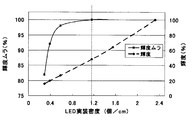
図12及びその結果をプロットした図14を参照すると、実施例であるパターン1に比して、何れのパターンも輝度は小さくなっている。一方でパターン1よりもLEDモジュール30の配置を疎としても、LEDモジュール30に大きな動作電流を流すことにより、LEDモジュール30の輝度を高めることができる。動作電流が大きくなることによって各LEDモジュール30の発熱量は増えるが、配置が疎であることにより、1のLEDモジュール30が他のLEDモジュール30に与える熱的な影響を抑えることができる。従って、パターン2及びパターン3については、輝度はパターン1に比して低下しているが、動作電流を高めることにより、輝度の低下を抑えることができ、十分実用に耐えうる。
次に、LEDモジュール30間の熱伝導について、LEDモジュール30間の温度を測定した。温度は、図15に示すように、発光しているLEDから一定距離離れたLEDの波長を測定し、LEDの実装密度と温度変化の関係を測定した。
結果を図16に示す。図16を参照すると、LED間の熱の影響を抑えるには、LEDモジュール30の実装密度は、2.32個/cm以下とすることが好適であることがわかる。
上記各データから、最適なLEDモジュール30の実装密度は、1.16個/cm~2.32個/cmであることが分かる。
本実施形態によれば、第1実施形態と同様の効果を奏する。加えて、LEDモジュール30は、導光板16の端面に対向して複数個配置されており、複数個のLEDモジュールは30、1.16個/cm~2.32個/cmの間隔で配置される。これにより、LEDモジュール30の実装密度が最適化され、画面の均一化を損なうことなく、高輝度且つ省電力なパネルユニットを提供できる。また、パネルユニット10の均一化、低コスト化も達成できる。また、省電力化が達成できることから、LEDモジュール30の冷却手段を簡易な構成とすることができ、パネルユニット10の薄型化や軽量化も達成できる。
<第3実施形態>
第1実施形態及び第2実施形態により、パネルユニット10の高輝度化、省電力化を達成できたが、LEDモジュール30は発光に伴って発熱するものであり、発生した熱を効率よく放熱する必要がある。放熱が効率よく行われない場合には、LEDモジュール30の温度が上昇してLEDモジュール30の信頼性が低くなり、発光効率が低下する虞があるためである。そこで本実施形態では、LEDモジュール30の放熱効率を高め、さらに高信頼性化を達成する。
第1実施形態及び第2実施形態により、パネルユニット10の高輝度化、省電力化を達成できたが、LEDモジュール30は発光に伴って発熱するものであり、発生した熱を効率よく放熱する必要がある。放熱が効率よく行われない場合には、LEDモジュール30の温度が上昇してLEDモジュール30の信頼性が低くなり、発光効率が低下する虞があるためである。そこで本実施形態では、LEDモジュール30の放熱効率を高め、さらに高信頼性化を達成する。
上述したようにLEDモジュール30はLEDバー40に所定間隔で配置される。また、LEDモジュール30は、LEDバー40の一方の面に配置され、LEDバー40の他方の面は、放熱板50と熱的に接触している。LEDモジュール30で発生した熱を効率よく放熱板50に伝熱するには、LEDモジュール30から放熱板50に至るまでの過程で熱効率を低くする必要がある。
LEDモジュール30から放熱板50に至るまでの過程で存在する熱抵抗は、各部材の熱抵抗であり、LEDチップ34の熱抵抗、配線パターン39の熱抵抗、絶縁層41の熱抵抗、LEDバー40の熱抵抗、及び、放熱板50の熱抵抗である(図5参照)。しかしながら各部材の熱抵抗は材質を変更しない限り低くすることは困難であるから、材質を変更しない場合に、全体として熱抵抗を低くするためには各部材間の伝熱効率を高める必要がある。
そこで本実施形態では図17に示すように、放熱板50と当接するLEDバー40の上記他方の面に、凹凸42が形成されている。LEDバー40に形成される凹凸42は、中心線平均粗さRaを10μm~25μmとすることが好適である。LEDバー40の凹凸42は、たとえば、LEDバー40を焼結により作製し、作製されたLEDバー40の放熱板50と接する面に研磨等の機械加工を施さないことにより形成することができる。また、凹凸42は、LEDバー40に粗面加工を施したり、ブラストやスパッタリングを施したりすることにより形成することもできる。
LEDバー40は、放熱板50に、半田(例えば、熱伝導率が高いSn-Pb系、Sn-Ag-Cu系、Sn-Zn-Al系、Sn-Bi-Ag系の半田)や熱伝導性に優れる接着剤、熱伝導性に優れる高分子テープなどにより熱的に接触するよう固定される。例えば、凹凸42が形成されて表面積が大きくなったLEDバー40と放熱板50とが錫系の半田により熱的に接触することで、LEDバー40から放熱板50に対する伝熱効率が高まる。これにより、LEDモジュール30の温度上昇を可及的に低減することができる。また、凹凸42を形成することにより、LEDバー40と放熱板50との接着強度を向上させることができる。
上述したように、放熱板50は、LEDモジュール30が内向きとなって導光板16の端面を照射可能となるようバックベゼル22に装着される。放熱板50は、外側面がバックベゼル22の内側面と熱的に接触し、内側面がLEDバー40に熱的に接触するように配置される。上述したように、バックベゼル22には、反射シート17及び導光板16が収容され、フロントベゼル20に嵌められる。
以下、LEDバー40の表面粗さ(Ra)と熱抵抗の関係について具体的に説明する。LEDバー40に対する加工として、凹凸42の表面粗さ(Ra)が(A)5μm、(B)10μm、(C)15μm、(D)20μm、(E)25μmのものを作製し、放熱板50と半田により熱的に接触するよう取り付けた。(A)においてLEDバー40と放熱板50との界面表面積は100μm2である。また、(B)においてLEDバー40と放熱板50との界面表面積220μm2である。また、(E)においてLEDバー40と放熱板50との界面表面積510μm2である。従って(A)と(B)の界面表面積を比較して分かるように、表面粗さ(Ra)を10μm~25μmとすることにより、凹凸加工を施さない場合(すなわち表面粗さ(Ra)が5μm以下の場合)に比して、放熱板50との界面表面積を2倍以上にできることがわかる。
さらにこれらについて全体の熱抵抗率(m2K/S・m-2)を測定した結果、上記(B)~(E)の凹凸42を形成したLEDバー40を備えたものは、上記(A)の凹凸42を形成したLEDバー40を備えたものに比して熱抵抗率を約50%以上低減できることが分かった。
なお、本実施形態では凹凸42をLEDバー40の他方の面(放熱板50に当接する面)に形成することとしたが、放熱板50の一方の面(LEDバー40に当接する面)に形成することとしてもよいし、LEDバー40と放熱板50の双方に形成することとしてもよい。
本実施形態によれば第1実施形態及び第2実施形態と同様の効果を奏する。加えて、放熱板50に当接するLEDバー40の他方の面および/またはLEDバー40に当接する放熱板50の一方の面の表面粗さを、中心線平均粗さRaで10μm~25μmとした。これにより、LEDバー40と放熱板50との接触界面の表面積を大きくすることにより、LEDバー40から放熱板50への放熱効率を高めることができるので、LEDモジュール30から発生する熱を効率的に放熱することができる。従って、LEDモジュール30に大電流を流すことが可能となり、バックライトユニット11及びこれを備えるパネルユニット10、さらにパネルユニット10を搭載した表示装置の高輝度化、高信頼性化を達成することができる。
<第4実施形態>
第3実施形態ではLEDモジュール30の放熱効率を高めるために、LEDバー40と放熱板50との接触界面の表面積を大きくすることによって、LEDバー40から放熱板50への放熱効率を高めた。LEDモジュール30の放熱効率を高める方法はこれに限られるものではなく、第3実施形態にて触れたように、部材の材質を最適化することとしてもよい。
第3実施形態ではLEDモジュール30の放熱効率を高めるために、LEDバー40と放熱板50との接触界面の表面積を大きくすることによって、LEDバー40から放熱板50への放熱効率を高めた。LEDモジュール30の放熱効率を高める方法はこれに限られるものではなく、第3実施形態にて触れたように、部材の材質を最適化することとしてもよい。
上記各実施形態では、LEDバー40に関して、アルミニウム若しくは銅板の上面にポリイミド系フィルムからなる絶縁層41を設けた構造としたが、本実施形態においてLEDバー40は、窒化アルミニウムなどの高熱伝導絶縁性セラミックスから構成される。
LEDバー40は、高熱伝導性を有し、絶縁性材料であるセラミックスから形成しているから、LEDモジュール30とLEDバー40との間に絶縁層を設ける必要がなく、LEDモジュール30を直接当接するよう配置することができる。従って、LEDモジュール30からLEDバー40への放熱効率を高めることができる。
図18は、LEDバー40に高熱伝導絶縁性セラミックスとして窒化アルミニウムを採用した本実施形態における各部材の熱伝導率を示す図である。図19は、LEDバー40に熱伝導性に優れる導電性のアルミニウムを採用し、LEDバー40とLEDモジュール30との間に絶縁層41を形成した比較例における各部材の熱伝導率を示す図である。図20は本実施形態と比較例の基板部分の等価熱伝導率を示す図である。
図18及び図19は共に、LEDチップ34としてGaNを使用し、LEDチップ34を配線パターン39に半田(Sn-Ag-Cu)を用いて電気的に接続される。従って、LEDチップ34、半田及び配線パターン39に関して熱伝導率に差は生じない。
一方、上述したように比較例では絶縁層41が設けられており、本実施形態では絶縁層が設けられていない。従って、絶縁層を有さない本実施形態が、絶縁層を有する比較例と比べて等価熱伝導率が低くなるのは明らかである。
加えて、図18及び図19に示すように、アルミニウムからなるLEDバー40の熱伝導率は、窒化アルミニウムからなるLEDバー40に比べて、熱伝導率が低い。このことからも本実施形態が、比較例と比べて等価熱伝導率が低くなるのは明らかである。
なお、図20に示す基板部分の等価熱伝導率(配線パターン39、絶縁層(比較例のみ)、LEDバー40の合成熱伝導率)は以下の数式により算出される。
等価熱伝導率(合成部分)=プリント配線板のトータルの厚さ[図17及び図18における(3)+(4)+(5)]/Σ{i層の厚さ/(i層の熱伝導率×i層の配線パターン残存率)}
なお、i層は(3)又は(4)又は(5)である。また、配線パターン残存率は、(4)及び(5)層を1とし、(3)層を0.18とした。
等価熱伝導率(合成部分)=プリント配線板のトータルの厚さ[図17及び図18における(3)+(4)+(5)]/Σ{i層の厚さ/(i層の熱伝導率×i層の配線パターン残存率)}
なお、i層は(3)又は(4)又は(5)である。また、配線パターン残存率は、(4)及び(5)層を1とし、(3)層を0.18とした。
具体的に、本実施形態の基板部分の等価熱伝導率は、図21(a)に示す数式により算出され、比較例の基板部分の等価熱伝導率は、図21(b)に示す数式により算出される。また、対比較比は、156/34.3×100=455%である。つまり、本実施形態は比較例に比して4倍以上の高熱伝導率を実現できる。
なお、比較例について、絶縁層41が介在していることによる温度上昇は、次により算出することができる。LEDチップ34の面積Aを0.5mm2(0.5mm×0.5mm×2個)、絶縁層のサイズ寄与率sを100%、絶縁層の厚さtを80μm、絶縁層の熱伝導率λを3W/m・Kとしたときに、熱抵抗Rは、R=(1/λ)・(t/A/s)により算出される。これによると、熱抵抗Rは53.3となる。
このとき、LEDモジュール30の電力Qを0.6W(6V、100mA)とすると、絶縁層が介在していることによるLEDモジュール30の温度上昇ΔTは、ΔT=R・Qにより算出でき、ΔTは32℃となる。一方、実施例については、比較例に比して温度上昇を1/5に抑えることができる。
本実施形態によれば第1実施形態及び第2実施形態と同様の効果を奏する。加えて、LEDバー40として、窒化アルミニウムを採用することにより、他の部材(アルミニウムや銅)を採用するのに比べて熱伝導率が高まり、LEDモジュール30から発生する熱を効率的に放熱することができる。従って、LEDモジュール30に大電流を流すことが可能となり、バックライトユニット11及びこれを備えるパネルユニット10、さらにパネルユニット10を搭載した表示装置の高輝度化、高信頼性化を達成することができる。
<第5実施形態>
第3実施形態及び第4実施形態では、LEDモジュール30で発生した熱を効率よく放熱板50に伝熱し、さらにバックベゼル22に伝熱することによって、LEDモジュール30の放熱効率を高めることとした。さらにLEDモジュール30の放熱効率を高めるには、バックベゼル22に伝わった熱をさらに他の部材に伝熱することが望ましい。
第3実施形態及び第4実施形態では、LEDモジュール30で発生した熱を効率よく放熱板50に伝熱し、さらにバックベゼル22に伝熱することによって、LEDモジュール30の放熱効率を高めることとした。さらにLEDモジュール30の放熱効率を高めるには、バックベゼル22に伝わった熱をさらに他の部材に伝熱することが望ましい。
そこで本実施形態では図22乃至図24に示すように、バックベゼル22の背面側に、ヒートパイプ60が配置される。ヒートパイプ60は、一端(高温部)がバックベゼル22と熱的に接触し、自由端側(冷却部)がバックベゼル22と接触しないように配置される。
より望ましくは、ヒートパイプ60は、一端がバックベゼル22を挟んで放熱板50と対向するように、バックベゼル22の短辺側端縁から内向きに設置される。
ヒートパイプ60は、バックベゼル22の短辺側端縁に複数配置することができ、放熱板50と対向するバックベゼル22の短辺側端縁からの熱を効率よく吸収することができるように、バックベゼル22の短辺側端縁の長さの60%から100%の範囲でヒートパイプ60と熱的に接触するようにすることが望ましい。すなわち、図23を参照して、バックベゼル22の短辺の長さをLb、ヒートパイプ60の短辺の長さをLpiとし、ヒートパイプ60をバックベゼル22の短辺方向に沿って6個縦に並べた際に、60(%)≦(Lp/Lb×100(%)≦100(%)、を満たすことが望ましい。なお、Lp=6×Lpiである。
ヒートパイプ60は、作動流体の蒸発、凝集による熱交換効率を高めるために、バックベゼル22と熱的に接触する高温部から自由端側の冷却部に向けて斜め上方に傾斜するよう配置することが好適である。
ヒートパイプ60は、コンテナ62の内部に作動流体を封入して構成することができる。作動流体として、アセトン水溶液を例示することができる。ヒートパイプ60は、コンテナ62を扁平形状としており、バックベゼル22に対して、その平坦面が広い面積で熱的に接触するようにしている。
また、ヒートパイプ60は、バックベゼル22と接触しない自由端側の冷却部がバックベゼル22から離れるように僅かに屈曲している。
図25は、設置されるヒートパイプ60の本数と、LEDモジュール30のジャンクション温度、輝度との関係を示す表である。なお、本実施形態は上述したようにヒートパイプ60の本数は6本である。ジャンクション温度は、pn接合部の最も高温となる部分の温度である。
図25を参照すると、ヒートパイプ60の設置本数を増やすことによって、LEDモジュール30のジャンクション温度を低下させることができることが分かる。また、LEDモジュール30の発熱を抑えることにより、LEDモジュール30の輝度を高めることができることが分かる。
図26及び図27は、バックベゼル22の短辺の長さLbとヒートパイプ60の短辺側の総長さLpの比を変えたときに、LEDモジュール30のジャンクション温度の変化を調べた表及びその結果を図示したグラフである。
図26及び図27を参照すると、Lp/Lbが大きくなる、即ち、ヒートパイプ60の短辺側の総長さが長くなる程、LEDモジュール30のジャンクション温度が低下していることがわかる。Lp/Lbが約0.6以上となることにより、ジャンクション温度を30℃以上低下させることができる。LEDモジュール30の発熱が抑えられることから、LEDモジュール30の輝度を高めることができる。
本実施形態によれば第3実施形態及び第4実施形態と同様の効果を奏する。加えて、バックベゼル22にヒートパイプ60を配置しているから、バックベゼル22の熱は、コンテナ62に伝達される。これにより、ヒートパイプ60は、高温部の内部で作動流体が熱を吸収して蒸発し、コンテナ62内を通って冷却部に移動する。冷却部に移動した作動流体は冷却されて凝集し、再度液体の状態となって、高温部に戻る。
このように、作動流体がコンテナ62内を循環することで、バックベゼル22からの吸熱を効率的に行なうことができ、LEDモジュール30の放熱効率を高めることができる。
<第6実施形態>
第5実施形態では、バックベゼル22に伝わった熱をヒートパイプ60に伝熱させることにより、LEDモジュール30の放熱効率を高めることとした。本実施形態では、さらにLEDモジュール30の放熱効率を高めるために、ヒートパイプ60に伝わった熱をさらに他の部材に伝熱する。
第5実施形態では、バックベゼル22に伝わった熱をヒートパイプ60に伝熱させることにより、LEDモジュール30の放熱効率を高めることとした。本実施形態では、さらにLEDモジュール30の放熱効率を高めるために、ヒートパイプ60に伝わった熱をさらに他の部材に伝熱する。
そこで本実施形態では図28に示すように、バックベゼル22の背面側がバックシャーシ23により覆われる。バックベゼル22とバックシャーシ23との間には、空隙が存在しており、バックベゼル22とバックシャーシ23は、ヒートパイプ60によって熱的に接続される。より詳細には、ヒートパイプ60は、一端(高温部)がバックベゼル22を挟んで放熱板50と対向するよう配置されて放熱板50と熱的に接触し、他端(冷却部)がバックシャーシ23と熱的に接触するよう配置される。
ヒートパイプ60は、第5実施形態にて示したように、複数配置することができる(図22乃至図24参照)。ヒートパイプ60は、バックベゼル22を挟んで放熱板50とバックシャーシ23とを高い熱交換効率で接続する。熱交換効率を高くするために、ヒートパイプ60は、コンテナ62の全表面積の8~18%が、バックシャーシ23と接触するように配置される。
ヒートパイプ60は、コンテナ62を扁平形状としており、バックベゼル22及びバックシャーシ23に対して、その平坦面が広い面積で熱的に接触するようにしている。
また、ヒートパイプ60は、バックベゼル22とバックシャーシ23との接触面積を大きく採るために、冷却部と高温部との間で段差が生じるように僅かに屈曲している。
ヒートパイプ60は、バックベゼル22及びバックシャーシ23に対し、高熱伝導樹脂による接着、半田付け、あるいは、図28に示すように、テープや金具などの抑え部材64により装着することができる。
図29は、ヒートパイプ60とバックシャーシ23との接触面積の割合を示す図であり、図30は図29に示す各比較例及び実施例とLEDモジュール30の温度低下率との関係を示している。図29において、放熱面積は一定(83cm2)であり、接触面積Scは、図28に示すように、ヒートパイプ60とバックシャーシ23が接触している部分の面積を示している。図29における実施例は、本開示の構造を適用した実施例、比較例は、比較のために作製した実施例である。なお、比較例1は、ヒートパイプ60を取り付けていない実施例である。
ヒートパイプ60の接触面積Scを変化させて、接触面積Sc/ヒートパイプ60の全面積Shを変えると、接触面積Scが小さくなるにつれて、LEDモジュール30の温度低下率が下がっていくことがわかる。しかしながら、図29及び図30を参照してわかるとおり、接触面積Sc/ヒートパイプ60の全面積Shが0.18(18%)を越えるとその効果は一旦飽和し、さらに0.08(8%)未満となると、再度温度低下率は悪化している。
従って、ヒートパイプ60とバックシャーシ23との接触面積は、ヒートパイプ60の全面積Shの8~18%となる状態で優れた熱交換効率を発揮できることがわかる。
本実施形態によれば第5実施形態と同様の効果を奏する。加えて、ヒートパイプ60の一端はバックベゼル22に熱的に接続され、他端はバックシャーシ23に熱的に接続されているから、バックベゼル22の熱は、コンテナ62を介してバックシャーシ23に伝達される。従って、LEDモジュール30の放熱効率をさらに高めることができる。
以上のように、本出願において開示する技術の例示として、実施の形態1~6を説明した。しかしながら、本開示における技術は、これに限定されず、変更、置き換え、付加、省略などを行った実施の形態にも適用できる。また、上記実施の形態1~6で説明した各構成要素を組み合わせて、新たな実施の形態とすることも可能である。
たとえば、液晶パネル12、拡散シート14、レンズシート15、導光板16の構成や構造、LEDバー40等の構成は、上記に限定されるものではない。
また、上記実施形態では、ヒートパイプ60と放熱板50との間にバックベゼル22を設けているが、バックベゼル22を省略し、ヒートパイプ60を放熱板50に直接接するように配置してもよい。
また、上記実施形態では、パネルユニットとしてエッジライト型パネルユニットとしたが直下ライト型パネルユニットであってもよい。
本開示は表示装置、パネルユニット及びバックライトユニットに利用可能である。
10 パネルユニット
12 液晶パネル
14 拡散シート
15 レンズシート
16 導光板
17 反射シート
18 配線
20 フロントベゼル
21 ミドルフレーム
22 バックベゼル
23 バックシャーシ
30 LEDモジュール
32 発光ダイオード
34 LEDチップ
36 蛍光体
38 電極ワイヤ
39 配線パターン
40 LEDバー
41 絶縁層
42 凹凸
50 放熱板
60 ヒートパイプ
62 コンテナ
64 抑え部材
12 液晶パネル
14 拡散シート
15 レンズシート
16 導光板
17 反射シート
18 配線
20 フロントベゼル
21 ミドルフレーム
22 バックベゼル
23 バックシャーシ
30 LEDモジュール
32 発光ダイオード
34 LEDチップ
36 蛍光体
38 電極ワイヤ
39 配線パターン
40 LEDバー
41 絶縁層
42 凹凸
50 放熱板
60 ヒートパイプ
62 コンテナ
64 抑え部材
Claims (11)
- 表示パネルと、
前記表示パネルの背面側に配置され、前記表示パネルへ光を導く導光板と、
前記導光板の端面に対向して配置され、青色の波長帯域と緑色の波長帯域とにスペクトルのピークを有する白色のLEDモジュールと、
前記導光板の背面側に配置され、光を反射する反射シートと、
を有する表示装置。 - 前記LEDモジュールは、420nm以上460nm以下の波長帯域に青色のスペクトルのピークを有しており、500nm以上600nm以下の波長帯域に緑色のスペクトルのピークを有する請求項1に記載の表示装置。
- 前記LEDモジュールは、青色の波長帯域におけるスペクトルのピーク強度をIbとし、緑色の波長帯域におけるスペクトルのピーク強度をIgとするとき、青色成分のピーク強度Ibと緑色成分のピーク強度Igのとの比が0.1≦Ig/Ib≦0.2である請求項1又は請求項2に記載の表示装置。
- 前記LEDモジュールは、前記導光板の一方向の両端の端面に対向して配置される請求項1に記載の表示装置。
- 前記LEDモジュールは、前記導光板の端面に対向して複数個配置されており、複数個のLEDモジュールは、1.16個/cm~2.32個/cmの間隔で配置される請求項4に記載の表示装置。
- 複数個の前記LEDモジュールを一方の面に搭載し、前記複数個のLEDモジュールから出射する光が前記導光板に入射するよう配置されたLEDバーと、前記LEDバーの他方の面と熱伝導可能に配置される放熱板と、をさらに有し、前記放熱板に当接する前記LEDバーの他方の面および/または前記LEDバーに当接する前記放熱板の一方の面の表面粗さは、中心線平均粗さRaで10μm~25μmである請求項1に記載の表示装置。
- 複数個の前記LEDモジュールを一方の面に搭載し、前記複数個のLEDモジュールから出射する光が前記導光板に入射するよう配置されたLEDバーをさらに有し、前記LEDバーは、高熱伝導絶縁性セラミックスから構成される請求項1に記載の表示装置。
- 複数個の前記LEDモジュールを一方の面に搭載し、前記複数個のLEDモジュールから出射する光が前記導光板に入射するよう配置されたLEDバーと、前記LEDバーの他方の面と熱伝導可能に配置される放熱板と、前記放熱板と熱伝導可能に配置され、前記導光板の背面側を覆う金属製のバックベゼルと、前記バックベゼルの前記導光板を覆う側とは反対側の面に配置され、扁平形状を有するコンテナの内部に作動流体が封入され、扁平形状の平坦な面が前記バックベゼルの前記反対側の面と接触するように設けられる複数のヒートパイプと、をさらに有する請求項1に記載の表示装置。
- 前記液晶パネルの背面側に配置され、端面から入射した光を一方の主面から出射して前記液晶パネルへ光を導く導光板と、
前記導光板の長手方向の両端の端面に対向して配置され、青色の波長帯域と緑色の波長帯域とにスペクトルのピークを有する白色のLEDモジュールと、
前記液晶パネルと前記導光板との間に間挿され、前記導光板から出射した光を拡散させる拡散シートと、
前記液晶パネルと前記導光板との間に間挿され、前記導光板から出射した光を集光するレンズシートと、
前記導光板の他方の主面に配置され、光を反射する反射シートと、
を有する表示装置。 - 表示パネルと、
前記表示パネルの背面側に配置され、前記表示パネルへ光を導く導光板と、
前記導光板の端面に対向して配置され、青色の波長帯域と緑色の波長帯域とにスペクトルのピークを有する白色のLEDモジュールと、
前記導光板の背面側に配置され、光を反射する反射シートと、
を有するパネルユニット。 - 表示パネルの背面側に配置され、前記表示パネルへ光を導く導光板と、
前記導光板の端面に対向して配置され、青色の波長帯域と緑色の波長帯域とにスペクトルのピークを有する白色のLEDモジュールと、
前記導光板の背面側に配置され、光を反射する反射シートと、
を有するバックライトユニット。
Applications Claiming Priority (12)
| Application Number | Priority Date | Filing Date | Title |
|---|---|---|---|
| JP2013-157619 | 2013-07-30 | ||
| JP2013-157618 | 2013-07-30 | ||
| JP2013157616A JP2016176965A (ja) | 2013-07-30 | 2013-07-30 | エッジライト型パネルユニット及びこれを具えた液晶表示装置 |
| JP2013157618A JP2016176966A (ja) | 2013-07-30 | 2013-07-30 | エッジライト型パネルユニット及びこれを具えた液晶表示装置 |
| JP2013157619A JP2016177866A (ja) | 2013-07-30 | 2013-07-30 | エッジライト型パネルユニット及びこれを具えた液晶表示装置 |
| JP2013157615A JP2016176964A (ja) | 2013-07-30 | 2013-07-30 | エッジライト型パネルユニット及びこれを具えた液晶表示装置 |
| JP2013-157617 | 2013-07-30 | ||
| JP2013157614A JP2016176963A (ja) | 2013-07-30 | 2013-07-30 | エッジライト型パネルユニット及びこれを具えた液晶表示装置 |
| JP2013157617A JP2016177865A (ja) | 2013-07-30 | 2013-07-30 | エッジライト型パネルユニット及びこれを具えた液晶表示装置 |
| JP2013-157616 | 2013-07-30 | ||
| JP2013-157614 | 2013-07-30 | ||
| JP2013-157615 | 2013-07-30 |
Publications (1)
| Publication Number | Publication Date |
|---|---|
| WO2015015805A1 true WO2015015805A1 (ja) | 2015-02-05 |
Family
ID=52431361
Family Applications (1)
| Application Number | Title | Priority Date | Filing Date |
|---|---|---|---|
| PCT/JP2014/004008 Ceased WO2015015805A1 (ja) | 2013-07-30 | 2014-07-30 | 表示装置、パネルユニット及びバックライトユニット |
Country Status (1)
| Country | Link |
|---|---|
| WO (1) | WO2015015805A1 (ja) |
Citations (5)
| Publication number | Priority date | Publication date | Assignee | Title |
|---|---|---|---|---|
| JP2004055772A (ja) * | 2002-07-18 | 2004-02-19 | Citizen Electronics Co Ltd | Led発光装置 |
| JP2006039341A (ja) * | 2004-07-29 | 2006-02-09 | Kyocera Corp | 液晶表示装置 |
| JP2010097908A (ja) * | 2008-10-20 | 2010-04-30 | Fujifilm Corp | バックライトユニットおよび液晶表示装置 |
| JP2011154956A (ja) * | 2010-01-28 | 2011-08-11 | Panasonic Corp | 光源装置、バックライトユニット、および液晶表示装置 |
| JP2012009793A (ja) * | 2010-06-28 | 2012-01-12 | Panasonic Corp | 発光装置、バックライトユニット、液晶表示装置及び照明装置 |
-
2014
- 2014-07-30 WO PCT/JP2014/004008 patent/WO2015015805A1/ja not_active Ceased
Patent Citations (5)
| Publication number | Priority date | Publication date | Assignee | Title |
|---|---|---|---|---|
| JP2004055772A (ja) * | 2002-07-18 | 2004-02-19 | Citizen Electronics Co Ltd | Led発光装置 |
| JP2006039341A (ja) * | 2004-07-29 | 2006-02-09 | Kyocera Corp | 液晶表示装置 |
| JP2010097908A (ja) * | 2008-10-20 | 2010-04-30 | Fujifilm Corp | バックライトユニットおよび液晶表示装置 |
| JP2011154956A (ja) * | 2010-01-28 | 2011-08-11 | Panasonic Corp | 光源装置、バックライトユニット、および液晶表示装置 |
| JP2012009793A (ja) * | 2010-06-28 | 2012-01-12 | Panasonic Corp | 発光装置、バックライトユニット、液晶表示装置及び照明装置 |
Similar Documents
| Publication | Publication Date | Title |
|---|---|---|
| KR102599014B1 (ko) | 색상 변환 어셈블리 및 그 제조 방법과 표시 패널 | |
| US7488104B2 (en) | Backlight unit and liquid crystal display device having the same | |
| US7478930B2 (en) | Backlight unit with an oxide compound-laminated optical layer | |
| US8746947B2 (en) | Backlight module, LCD device and light source of backlight module | |
| JP6157738B2 (ja) | バックライトモジュール及び前記バックライトモジュールを用いた液晶表示モジュール | |
| WO2010100786A1 (ja) | 光源装置および液晶表示装置 | |
| KR101656100B1 (ko) | 다층 인쇄회로기판 및 이를 포함하는 액정표시장치 | |
| KR20160117026A (ko) | 디스플레이 장치 | |
| JP2009252380A (ja) | 中空式面照明装置 | |
| WO2016169233A1 (zh) | Led灯条、背光源及显示装置 | |
| JP4862667B2 (ja) | 光源モジュール及び光源装置 | |
| JP2008288228A (ja) | 発光装置、光源装置、及び液晶表示装置 | |
| WO2012073750A1 (ja) | 照明装置、表示装置、及びテレビ受信装置 | |
| US20200161509A1 (en) | Quantum-dot led backlight module for led displays | |
| US11789312B2 (en) | Lighting device and display device | |
| JP5755928B2 (ja) | バックライトユニット | |
| US8128266B2 (en) | Edge-light backlight assembly | |
| KR102047223B1 (ko) | 엘이디를 사용하는 백라이트유닛 및 이를 포함하는 액정표시장치 | |
| KR101729776B1 (ko) | 백라이트 유닛 및 이를 구비한 액정표시장치 | |
| JP4912844B2 (ja) | 発光装置、およびこれを用いた表示装置 | |
| CN114397780A (zh) | 一种背光源模组及显示装置 | |
| JP2010231974A (ja) | 照明装置、面照明装置及び発光装置 | |
| KR101984080B1 (ko) | 백라이트 유닛 | |
| KR100742125B1 (ko) | 백 라이트 유닛 | |
| KR20110135553A (ko) | 백라이트 유닛 및 이를 포함하는 디스플레이 장치 |
Legal Events
| Date | Code | Title | Description |
|---|---|---|---|
| 121 | Ep: the epo has been informed by wipo that ep was designated in this application |
Ref document number: 14831362 Country of ref document: EP Kind code of ref document: A1 |
|
| NENP | Non-entry into the national phase |
Ref country code: DE |
|
| 122 | Ep: pct application non-entry in european phase |
Ref document number: 14831362 Country of ref document: EP Kind code of ref document: A1 |
|
| NENP | Non-entry into the national phase |
Ref country code: JP |