WO2015005176A1 - Display device and light diffusing member - Google Patents
Display device and light diffusing member Download PDFInfo
- Publication number
- WO2015005176A1 WO2015005176A1 PCT/JP2014/067513 JP2014067513W WO2015005176A1 WO 2015005176 A1 WO2015005176 A1 WO 2015005176A1 JP 2014067513 W JP2014067513 W JP 2014067513W WO 2015005176 A1 WO2015005176 A1 WO 2015005176A1
- Authority
- WO
- WIPO (PCT)
- Prior art keywords
- light
- substrate
- shielding layer
- light shielding
- display device
- Prior art date
Links
Images


Classifications
-
- G—PHYSICS
- G02—OPTICS
- G02B—OPTICAL ELEMENTS, SYSTEMS OR APPARATUS
- G02B5/00—Optical elements other than lenses
- G02B5/02—Diffusing elements; Afocal elements
- G02B5/0273—Diffusing elements; Afocal elements characterized by the use
- G02B5/0294—Diffusing elements; Afocal elements characterized by the use adapted to provide an additional optical effect, e.g. anti-reflection or filter
-
- G—PHYSICS
- G02—OPTICS
- G02B—OPTICAL ELEMENTS, SYSTEMS OR APPARATUS
- G02B5/00—Optical elements other than lenses
- G02B5/02—Diffusing elements; Afocal elements
- G02B5/0205—Diffusing elements; Afocal elements characterised by the diffusing properties
- G02B5/021—Diffusing elements; Afocal elements characterised by the diffusing properties the diffusion taking place at the element's surface, e.g. by means of surface roughening or microprismatic structures
- G02B5/0226—Diffusing elements; Afocal elements characterised by the diffusing properties the diffusion taking place at the element's surface, e.g. by means of surface roughening or microprismatic structures having particles on the surface
-
- G—PHYSICS
- G02—OPTICS
- G02B—OPTICAL ELEMENTS, SYSTEMS OR APPARATUS
- G02B5/00—Optical elements other than lenses
- G02B5/02—Diffusing elements; Afocal elements
- G02B5/0205—Diffusing elements; Afocal elements characterised by the diffusing properties
- G02B5/021—Diffusing elements; Afocal elements characterised by the diffusing properties the diffusion taking place at the element's surface, e.g. by means of surface roughening or microprismatic structures
- G02B5/0231—Diffusing elements; Afocal elements characterised by the diffusing properties the diffusion taking place at the element's surface, e.g. by means of surface roughening or microprismatic structures the surface having microprismatic or micropyramidal shape
-
- G—PHYSICS
- G02—OPTICS
- G02B—OPTICAL ELEMENTS, SYSTEMS OR APPARATUS
- G02B5/00—Optical elements other than lenses
- G02B5/02—Diffusing elements; Afocal elements
- G02B5/0205—Diffusing elements; Afocal elements characterised by the diffusing properties
- G02B5/0257—Diffusing elements; Afocal elements characterised by the diffusing properties creating an anisotropic diffusion characteristic, i.e. distributing output differently in two perpendicular axes
-
- G—PHYSICS
- G02—OPTICS
- G02B—OPTICAL ELEMENTS, SYSTEMS OR APPARATUS
- G02B5/00—Optical elements other than lenses
- G02B5/02—Diffusing elements; Afocal elements
- G02B5/0273—Diffusing elements; Afocal elements characterized by the use
- G02B5/0278—Diffusing elements; Afocal elements characterized by the use used in transmission
-
- G—PHYSICS
- G02—OPTICS
- G02B—OPTICAL ELEMENTS, SYSTEMS OR APPARATUS
- G02B5/00—Optical elements other than lenses
- G02B5/30—Polarising elements
- G02B5/3025—Polarisers, i.e. arrangements capable of producing a definite output polarisation state from an unpolarised input state
- G02B5/3033—Polarisers, i.e. arrangements capable of producing a definite output polarisation state from an unpolarised input state in the form of a thin sheet or foil, e.g. Polaroid
-
- G—PHYSICS
- G02—OPTICS
- G02F—OPTICAL DEVICES OR ARRANGEMENTS FOR THE CONTROL OF LIGHT BY MODIFICATION OF THE OPTICAL PROPERTIES OF THE MEDIA OF THE ELEMENTS INVOLVED THEREIN; NON-LINEAR OPTICS; FREQUENCY-CHANGING OF LIGHT; OPTICAL LOGIC ELEMENTS; OPTICAL ANALOGUE/DIGITAL CONVERTERS
- G02F1/00—Devices or arrangements for the control of the intensity, colour, phase, polarisation or direction of light arriving from an independent light source, e.g. switching, gating or modulating; Non-linear optics
- G02F1/01—Devices or arrangements for the control of the intensity, colour, phase, polarisation or direction of light arriving from an independent light source, e.g. switching, gating or modulating; Non-linear optics for the control of the intensity, phase, polarisation or colour
- G02F1/13—Devices or arrangements for the control of the intensity, colour, phase, polarisation or direction of light arriving from an independent light source, e.g. switching, gating or modulating; Non-linear optics for the control of the intensity, phase, polarisation or colour based on liquid crystals, e.g. single liquid crystal display cells
- G02F1/133—Constructional arrangements; Operation of liquid crystal cells; Circuit arrangements
- G02F1/1333—Constructional arrangements; Manufacturing methods
- G02F1/1335—Structural association of cells with optical devices, e.g. polarisers or reflectors
- G02F1/133504—Diffusing, scattering, diffracting elements
-
- G—PHYSICS
- G02—OPTICS
- G02F—OPTICAL DEVICES OR ARRANGEMENTS FOR THE CONTROL OF LIGHT BY MODIFICATION OF THE OPTICAL PROPERTIES OF THE MEDIA OF THE ELEMENTS INVOLVED THEREIN; NON-LINEAR OPTICS; FREQUENCY-CHANGING OF LIGHT; OPTICAL LOGIC ELEMENTS; OPTICAL ANALOGUE/DIGITAL CONVERTERS
- G02F1/00—Devices or arrangements for the control of the intensity, colour, phase, polarisation or direction of light arriving from an independent light source, e.g. switching, gating or modulating; Non-linear optics
- G02F1/01—Devices or arrangements for the control of the intensity, colour, phase, polarisation or direction of light arriving from an independent light source, e.g. switching, gating or modulating; Non-linear optics for the control of the intensity, phase, polarisation or colour
- G02F1/13—Devices or arrangements for the control of the intensity, colour, phase, polarisation or direction of light arriving from an independent light source, e.g. switching, gating or modulating; Non-linear optics for the control of the intensity, phase, polarisation or colour based on liquid crystals, e.g. single liquid crystal display cells
- G02F1/133—Constructional arrangements; Operation of liquid crystal cells; Circuit arrangements
- G02F1/1333—Constructional arrangements; Manufacturing methods
- G02F1/1335—Structural association of cells with optical devices, e.g. polarisers or reflectors
- G02F1/133509—Filters, e.g. light shielding masks
- G02F1/133512—Light shielding layers, e.g. black matrix
-
- G—PHYSICS
- G02—OPTICS
- G02F—OPTICAL DEVICES OR ARRANGEMENTS FOR THE CONTROL OF LIGHT BY MODIFICATION OF THE OPTICAL PROPERTIES OF THE MEDIA OF THE ELEMENTS INVOLVED THEREIN; NON-LINEAR OPTICS; FREQUENCY-CHANGING OF LIGHT; OPTICAL LOGIC ELEMENTS; OPTICAL ANALOGUE/DIGITAL CONVERTERS
- G02F1/00—Devices or arrangements for the control of the intensity, colour, phase, polarisation or direction of light arriving from an independent light source, e.g. switching, gating or modulating; Non-linear optics
- G02F1/01—Devices or arrangements for the control of the intensity, colour, phase, polarisation or direction of light arriving from an independent light source, e.g. switching, gating or modulating; Non-linear optics for the control of the intensity, phase, polarisation or colour
- G02F1/13—Devices or arrangements for the control of the intensity, colour, phase, polarisation or direction of light arriving from an independent light source, e.g. switching, gating or modulating; Non-linear optics for the control of the intensity, phase, polarisation or colour based on liquid crystals, e.g. single liquid crystal display cells
- G02F1/133—Constructional arrangements; Operation of liquid crystal cells; Circuit arrangements
- G02F1/1333—Constructional arrangements; Manufacturing methods
- G02F1/1335—Structural association of cells with optical devices, e.g. polarisers or reflectors
- G02F1/133528—Polarisers
-
- G—PHYSICS
- G03—PHOTOGRAPHY; CINEMATOGRAPHY; ANALOGOUS TECHNIQUES USING WAVES OTHER THAN OPTICAL WAVES; ELECTROGRAPHY; HOLOGRAPHY
- G03F—PHOTOMECHANICAL PRODUCTION OF TEXTURED OR PATTERNED SURFACES, e.g. FOR PRINTING, FOR PROCESSING OF SEMICONDUCTOR DEVICES; MATERIALS THEREFOR; ORIGINALS THEREFOR; APPARATUS SPECIALLY ADAPTED THEREFOR
- G03F7/00—Photomechanical, e.g. photolithographic, production of textured or patterned surfaces, e.g. printing surfaces; Materials therefor, e.g. comprising photoresists; Apparatus specially adapted therefor
- G03F7/0005—Production of optical devices or components in so far as characterised by the lithographic processes or materials used therefor
-
- G—PHYSICS
- G03—PHOTOGRAPHY; CINEMATOGRAPHY; ANALOGOUS TECHNIQUES USING WAVES OTHER THAN OPTICAL WAVES; ELECTROGRAPHY; HOLOGRAPHY
- G03F—PHOTOMECHANICAL PRODUCTION OF TEXTURED OR PATTERNED SURFACES, e.g. FOR PRINTING, FOR PROCESSING OF SEMICONDUCTOR DEVICES; MATERIALS THEREFOR; ORIGINALS THEREFOR; APPARATUS SPECIALLY ADAPTED THEREFOR
- G03F7/00—Photomechanical, e.g. photolithographic, production of textured or patterned surfaces, e.g. printing surfaces; Materials therefor, e.g. comprising photoresists; Apparatus specially adapted therefor
- G03F7/20—Exposure; Apparatus therefor
-
- G—PHYSICS
- G03—PHOTOGRAPHY; CINEMATOGRAPHY; ANALOGOUS TECHNIQUES USING WAVES OTHER THAN OPTICAL WAVES; ELECTROGRAPHY; HOLOGRAPHY
- G03F—PHOTOMECHANICAL PRODUCTION OF TEXTURED OR PATTERNED SURFACES, e.g. FOR PRINTING, FOR PROCESSING OF SEMICONDUCTOR DEVICES; MATERIALS THEREFOR; ORIGINALS THEREFOR; APPARATUS SPECIALLY ADAPTED THEREFOR
- G03F7/00—Photomechanical, e.g. photolithographic, production of textured or patterned surfaces, e.g. printing surfaces; Materials therefor, e.g. comprising photoresists; Apparatus specially adapted therefor
- G03F7/26—Processing photosensitive materials; Apparatus therefor
- G03F7/30—Imagewise removal using liquid means
- G03F7/32—Liquid compositions therefor, e.g. developers
Definitions
- the present invention relates to a display device and a light diffusing member.
- Liquid crystal display devices are widely used as portable electronic devices such as cellular phones or displays for televisions, personal computers, and the like.
- liquid crystal display devices are known to have excellent visibility from the front, but have a narrow viewing angle.
- Various devices have been devised for widening the viewing angle.
- One example is a configuration in which a member for diffusing light emitted from a display body such as a liquid crystal panel (hereinafter referred to as “light diffusing member”) is provided on the viewing side of the display body.
- optical sheet comprising a base film layer, an optical functional sheet layer disposed on the base film layer, and a diffusing material-containing layer (light diffusing layer) disposed on the optical functional sheet layer
- the optical functional sheet layer has a substantially trapezoidal prism portion formed in parallel along the upper surface of the base film layer, and the light absorbing portion is provided in a substantially wedge-shaped portion between the prism portions. It is an arranged configuration.
- a light-transmitting base material a plurality of light-shielding layers formed on one surface of the base material, and a light diffusion portion formed in a region other than the region where the light-shielding layer is formed on one surface of the base material.
- Provided light diffusing members have been developed.
- the arrangement of the light shielding layer is not random and is affixed to the display surface of the liquid crystal panel to constitute a liquid crystal display device, the arrangement of the light shielding layer and the pixel pitch of the liquid crystal panel are Due to the interference, the moire interference fringes are strongly recognized, and the display characteristics of the liquid crystal display device are deteriorated.
- An object of the present invention is to provide a display device that can reduce the occurrence of moire interference fringes due to interference between the arrangement of light shielding layers and the pixel pitch of a liquid crystal panel, a method for manufacturing the same, and a light diffusing member.
- a display device includes a base material having light transmittance, a plurality of light-shielding layers formed on one surface of the base material with a repeating cycle, and the light-shielding layer on one surface of the base material.
- a light diffusing portion formed in a region other than the forming region, and the light diffusing portion has a light emitting end surface on the base material side and an area of the light emitting end surface opposite to the base material side.
- a periodic direction in which the light incident end face has a large area, the height from the light incident end face to the light exit end face of the light diffusion portion is larger than the thickness of the light shielding layer, and the light shielding layer is repeatedly formed.
- the pixel pitch direction of the display body are non-parallel.
- a display device includes a light-transmitting base material, a plurality of light-shielding layers formed on one surface of the base material, and a region other than a region where the light-shielding layer is formed on one surface of the base material
- a light diffusing portion formed in the region, and the light diffusing portion has a light emitting end face on the substrate side and an area larger than the area of the light emitting end face on the side opposite to the substrate side.
- a light incident end face, a height from the light incident end face of the light diffusing portion to the light exit end face is larger than a layer thickness of the light shielding layer, a periodic direction in which the light shielding layer is arranged, and a display body
- the pixel pitch direction is non-parallel, and the period in which the light shielding layers are arranged is smaller than the pixel pitch.
- the light diffusing member includes a light-transmitting base material, a plurality of light-shielding layers formed on one surface of the base material with a repeating period, and the one surface of the base material.
- a light diffusing portion formed in a region other than the region where the light shielding layer is formed, and the light diffusing portion has a light emitting end surface on the substrate side and the light emitting end surface on the side opposite to the substrate side.
- a light incident end face having an area larger than the area, and a height from the light incident end face to the light exit end face of the light diffusion portion is larger than a layer thickness of the light shielding layer,
- the scattering intensity of the light diffusion portion viewed from the direction is an anisotropic light diffusion member having a strong scattering direction and a weak scattering direction, and the strong scattering direction of the light diffusion portion and the periodic direction in which the light shielding layer is formed repeatedly Are non-parallel.
- a light diffusing member includes a light-transmitting base material, a plurality of light shielding layers formed on one surface of the base material, and a region where the light shielding layer is formed on one surface of the base material.
- a light diffusing portion formed in a region other than the above, and the light diffusing portion has a light emitting end surface on the substrate side and an area larger than the area of the light emitting end surface on the side opposite to the substrate side The height from the light incident end surface of the light diffusing portion to the light emitting end surface of the light diffusing portion is larger than the layer thickness of the light shielding layer, and is viewed from the normal direction of one surface of the substrate.
- the scattering intensity of the light diffusion portion is an anisotropic light diffusion member having a strong scattering direction and a weak scattering direction, and the strong scattering direction of the light diffusion portion and the periodic direction in which the light shielding layers are arranged are non-parallel.
- a display device includes a light-transmitting base material, a plurality of light-shielding layers formed on one surface of the base material, and a region other than a region where the light-shielding layer is formed on one surface of the base material
- a light diffusing portion formed in the region, and the light diffusing portion has a light emitting end face on the substrate side and an area larger than the area of the light emitting end face on the side opposite to the substrate side.
- the scattering intensity of the diffusion part is an anisotropic light diffusion member having a strong scattering direction and a weak scattering direction, and the strong scattering direction of the light diffusion part and the periodic direction in which the light shielding layer is arranged are non-parallel,
- the periodic direction in which the light shielding layers are arranged is not parallel to the pixel pitch direction of the display body. Period where the light-shielding layer is arranged is smaller than the pixel pitch.
- a light-transmitting base material a plurality of light diffusion portions formed on one surface of the base material with a repeating cycle, and one surface of the base material,
- a light shielding layer formed in a region other than the region where the light diffusing portion is formed, and the light diffusing portion has a light emitting end surface on the substrate side and the light emitting end surface on the opposite side to the substrate side.
- a light incident end face having an area larger than the area of the light diffusing section, and a height from the light incident end face of the light diffusing section to the light emitting end face is larger than a layer thickness of the light shielding layer, and the light diffusing section repeats The periodic direction to be formed and the pixel pitch direction of the display body are non-parallel.
- a display device includes a light-transmitting base material, a plurality of light diffusion portions formed on one surface of the base material, and the formation of the light diffusion portion on one surface of the base material.
- a light-shielding layer formed in a region other than the region, and the light diffusion portion has a light emission end surface on the substrate side and an area larger than the area of the light emission end surface on the side opposite to the substrate side
- a periodic direction in which the height from the light incident end surface of the light diffusing portion to the light emitting end surface is larger than the thickness of the light shielding layer, and the light diffusing portions are arranged, and a display
- the pixel pitch direction of the body is non-parallel, and the period in which the light diffusion portions are arranged is smaller than the pixel pitch.
- a light diffusing member includes a light-transmitting base material, a plurality of light diffusing portions formed on one surface of the base material with a repeating cycle, and one surface of the base material.
- a light shielding layer formed in a region other than the region where the light diffusing portion is formed, and the light diffusing portion has a light emitting end surface on the substrate side and the light emitting end surface on the opposite side to the substrate side.
- a light incident end face having an area larger than the area of the light diffusion portion, and a height from the light incident end face to the light exit end face of the light diffusing portion is larger than a layer thickness of the light shielding layer.
- the light diffusing part is an anisotropic light diffusing member having a scattering intensity of the light diffusing part viewed from the line direction and having a strong scattering direction and a weak scattering direction, and the strong diffusing direction of the light diffusing part and the light diffusing part are formed repeatedly.
- the periodic direction is non-parallel.
- a light diffusing member includes a light-transmitting base material, a plurality of light diffusing portions formed on one surface of the base material, and the formation of the light shielding layer on the one surface of the base material.
- a light-shielding layer formed in a region other than the region, and the light diffusion portion has a light emission end surface on the substrate side and an area larger than the area of the light emission end surface on the side opposite to the substrate side
- the height from the light incident end surface of the light diffusing portion to the light emitting end surface of the light diffusing portion is larger than the layer thickness of the light shielding layer, and is viewed from the normal direction of one surface of the substrate.
- the scattering intensity of the light diffusion part is an anisotropic light diffusion member having a strong scattering direction and a weak scattering direction, and the strong scattering direction of the light diffusion part and the periodic direction in which the light diffusion parts are arranged are non-parallel .
- a display device includes a light-transmitting base material, a plurality of light diffusion portions formed on one surface of the base material, and a formation region of the light shielding layer on the one surface of the base material.
- a light-shielding layer formed in a region other than the above, and the light diffusing portion has a light emission end face on the substrate side and an area larger than the area of the light emission end face on the opposite side to the substrate side.
- the scattering intensity of the diffusion part is an anisotropic light diffusion member having a strong scattering direction and a weak scattering direction, and the strong scattering direction of the light diffusion part and the periodic direction in which the light diffusion parts are arranged are non-parallel,
- the periodic direction in which the light diffusion portions are arranged and the pixel pitch direction of the display body are non-parallel. Ri, period where the light diffusing portion is arranged is smaller than the pixel pitch.
- At least one of an antireflection layer, an antistatic layer, an antiglare treatment layer, and an antifouling treatment layer is provided on the surface opposite to the one surface of the base material.
- the strong scattering direction of the light diffusing portion and the diagonal line connecting the apexes of the display body are non-parallel.
- a polarizing plate is provided between the base material and the display body, and between the base material and the polarizing plate, between the refractive index of the base material and the refractive index of the polarizing plate. It is preferable that a member having a refractive index of 5 is interposed.
- a part of the surface of the light shielding layer on the side opposite to the base material is covered with a light scattering member.
- the planar shape of the light shielding layer viewed from the normal direction of one surface of the substrate is an anisotropic shape having a major axis and a minor axis.
- the planar shape of the light shielding layer viewed from the normal direction of one surface of the substrate is an ellipse or a polygon.
- the plurality of light shielding layers include light shielding layers having different sizes.
- a space defined by the light shielding layer and the side surface of the light diffusion portion is a hollow portion, and the hollow portion is filled with a gas.
- an inclination angle of a side surface of at least one of the plurality of light diffusion portions is different from an inclination angle of a side surface of the other light diffusion portion.
- an inclination angle of a side surface of at least one of the plurality of light diffusion portions is different depending on a place.
- the planar shape of the light shielding layer viewed from the normal direction of one surface of the base material is an isotropic shape
- the side surface shape of the light shielding layer has an anisotropy having a major axis and a minor axis. The shape is preferred.
- a method for manufacturing a display device includes a step of forming a plurality of light-shielding layers with a repeating cycle on one surface of a light-transmitting base material, A step of forming a light-sensitive negative photosensitive resin layer so as to cover the light-shielding layer, and a surface opposite to one surface of the substrate on which the light-shielding layer and the negative photosensitive resin layer are formed, The step of irradiating the negative photosensitive resin layer with diffused light through a region other than the region where the light shielding layer is formed to expose the negative photosensitive resin layer, and the exposure of the negative photosensitive resin layer after the exposure.
- a light diffusing portion having a light incident end face having an area larger than the area of the light emitting end face on the opposite side of the base material side on the one side of the base material.
- a step of sticking a polarizing plate through an adhesive, and a laminate including the base material, the light shielding layer, the light diffusing portion, and the polarizing plate are cut along the thickness direction,
- a method for manufacturing a display device including: a step of forming a light-shielding layer having an opening with a repetition period on one surface of a light-transmitting substrate; A step of forming a light-sensitive negative photosensitive resin layer so as to cover the light-shielding layer, and a surface opposite to the one surface of the substrate on which the light-shielding layer and the negative photosensitive resin layer are formed. Irradiating the negative photosensitive resin layer with diffused light through the opening of the light shielding layer to expose the negative photosensitive resin layer; and the exposure of the negative photosensitive resin layer after the exposure.
- the method for manufacturing a display device includes a step of forming a light-shielding layer having a repeating cycle on one surface of a light-transmitting substrate, and the light-shielding layer on one surface of the substrate.
- moire interference fringes are not noticeable in the display device, and the visibility of the display device can be improved.
- FIG. It is the schematic which shows the liquid crystal display device of 11th embodiment, (A) is sectional drawing of the liquid crystal display device of 11th embodiment, (B), (C) is the liquid crystal display device of 11th embodiment.
- FIG. It is sectional drawing of the light-diffusion member of 11th embodiment.
- Embodiments of a display device, a manufacturing method thereof, and a light diffusion member of the present invention will be described. Note that this embodiment is specifically described in order to better understand the gist of the invention, and does not limit the present invention unless otherwise specified.
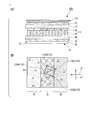
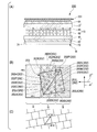
- FIG. 1 is a schematic diagram illustrating a liquid crystal display device according to the present embodiment.
- FIG. 1A is a cross-sectional view of the liquid crystal display device according to the present embodiment.
- FIG. 1B is a plan view of the liquid crystal display device according to the present embodiment.
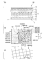
- FIG. 2 is a cross-sectional view of the light diffusing member of this embodiment.
- a liquid crystal display device (display device) 10 according to the present embodiment is schematically configured from a backlight (light source) 11, a first polarizing plate 12, a liquid crystal panel 13, a second polarizing plate 14, and a light diffusion member 15. ing.
- the liquid crystal panel 13 is schematically illustrated as a single plate, but the detailed structure thereof will be described later.
- the observer views the display from the upper side of the liquid crystal display device 10 in FIG. 1 in which the light diffusing member 15 is arranged. Therefore, in the following description, the side on which the light diffusing member 15 is disposed is referred to as a viewing side, and the side on which the backlight 11 is disposed is referred to as a back side.
- the arrow ⁇ is the transmission axis direction of the first polarizing plate 12
- the arrow ⁇ is the transmission axis direction of the second polarizing plate 14
- the arrow ⁇ is the clear viewing direction (asymmetric direction)
- the arrow ⁇ is light.
- the direction in which the scattering intensity of the diffusing member 15 is strong is shown.
- the light emitted from the backlight 11 is modulated by the liquid crystal panel 13, and a predetermined image, character, or the like is displayed by the modulated light. Further, when the light emitted from the liquid crystal panel 13 passes through the light diffusion member 15, the angle distribution of the emitted light becomes wider than before entering the light diffusion member 15, and the light is emitted from the light diffusion member 15. The Thereby, the observer can visually recognize the display with a wide viewing angle.
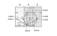
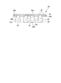
- the liquid crystal panel 13 includes a TFT substrate 16 on which switching elements and the like are formed, a color filter substrate 17 disposed to face the TFT substrate 16, and a liquid crystal layer sandwiched between the TFT substrate 16 and the color filter substrate 17. 18.
- a color filter 19 including red (R), green (G), and blue (B) pigments is provided on the surface of the color filter substrate 17 facing the liquid crystal layer 18.
- the light diffusing member 15 includes a light-transmitting base material 20, a plurality of light shielding layers 21 formed on one surface (back surface) 20 a of the base material 20, and one surface 20 a of the base material 20.
- the light diffusion portion 22 is formed in a region other than the region where the light shielding layer 21 is formed, and the light scattering layer 23 is formed on the other surface (surface on the viewing side) 20b of the substrate 20.
- the light diffusion portion 15 has a light emission end face 22a on the base material 20 side and a light incident end face 22b having an area larger than the area of the light emission end face 22a on the side opposite to the base material 20 side.
- the height from the light incident end face 22 a to the light exit end face 22 b of the light diffusing portion 15 is larger than the thickness of the light shielding layer 21.
- a space defined by the light shielding layer 21 and the side surface 22c of the light diffusion portion 22 is a hollow portion 24, and the hollow portion 24 is filled with a gas such as air.
- At least one of an antireflection layer, a polarizing filter layer, an antistatic layer, an antiglare treatment layer, and an antifouling treatment layer is provided on the viewing side of the base material 20 of the light diffusion member 15 (the side opposite to the one surface 20a). It is good also as a structure which provided. According to this configuration, it is possible to add a function of reducing external light reflection, a function of preventing adhesion of dust and dirt, a function of preventing scratches, and the like according to the type of layer provided on the viewing side of the substrate 20. And deterioration of viewing angle characteristics with time can be prevented.
- the inclination angle of the side surface 22c of the light diffusion portion 22 (the angle formed by the one surface 20a of the base material 20 and the side surface 22c of the light diffusion portion 22) is preferably 60 ° or greater and 90 ° or less.
- the inclination angle of the side surface 22c of the light diffusion portion 22 is not particularly limited as long as it is an angle that can sufficiently diffuse incident light when emitted from the light diffusion member 15.
- the light diffusion portion 22 has a large number of side surfaces 22c in the hollow portion 24, and the inclination angle of the side surfaces 22c is constant. It is not limited. Of the multiple side surfaces 22c, at least one inclination angle may be different from the inclination angle of the other side surface 22c. In addition, at least one of the side surfaces 22c may have different inclination angles depending on the location.
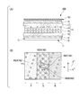
- the planar shape of the light shielding layer 21 viewed from the normal direction of the other surface (surface on the viewing side) 20b of the base material 20 is at least a long axis. And has a short axis and an anisotropic shape (elongated elliptical shape).
- the light shielding layer 21 is arranged with a predetermined period. For example, as shown in FIG. 1B, around one dot 21 ⁇ / b> A of the light shielding layer 21, there are six dots 21 ⁇ / b> B of the light shielding layer 21 around it. , 21C, 21D, 21E, 21F, 21G are arranged.
- the dots 21B, 21C, 21D, 21E, 21F, 21G and the like constituting the light shielding layer 21 are arranged to form a hexagonal close-packed structure. Further, these six dots 21B, 21C, 21D, 21E, 21F, and 21G are arranged in six rotational symmetry.
- the light shielding layer 21, that is, the periodic direction in which the dots 21A, 21B, 21C, 21D, 21E, 21F, and 21G constituting the light shielding layer 21 are repeatedly formed, and the pixel pitch direction of the liquid crystal panel 13 Are non-parallel.
- the pixel pitch of the liquid crystal panel 13 refers to PP1 that is the interval between the red (R), green (G), and blue (B) dyes, and the width of each dye. It is PP2 that is.
- PP1 the interval between the red (R), green (G), and blue (B) dyes, and the width of each dye.
- PP2 that is.
- the direction of the pixel pitch PP1 and the direction of the pixel pitch PP2 are non-parallel. Further, the direction of the pixel pitch PP1 and the direction of the pixel pitch PP2 are not parallel to the distance (pitch) direction DP2 from the dot 21A to the dot 21H that is second closest to the dot 21A.
- the direction of the pixel pitch PP1 and the distance (pitch) direction DP1-b from the dot 21A to the dot 21B closest to the dot 21A are non-parallel.
- the direction of the pixel pitch PP1 is not parallel to the distance (pitch) directions DP1-a and DP1-c from the dot 21A to the dots 21C and 21G that are second closest to the dot 21A.
- the distance (pitch) direction DP2 from the dot 21A to the closest dot 21H beyond the hexagonal close-packed structure and the direction of the pixel pitch PP1. -B is non-parallel.
- the distance (pitch) directions DP2-a and DP2-c from the dot 21A to the dots 21I and 21J that are second closest to the direction beyond the hexagonal close-packed structure in the direction of the pixel pitch PP1. are non-parallel.
- the direction of the pixel pitch PP2 and the moving direction DP1-b from the dot 21A to the dot 21B closest to the dot 21A are non-parallel.
- the direction of the pixel pitch PP2 and the distance (pitch) directions DP1-a and DP1-c from the dot 21A to the dots 21C and 21G that are second closest to the dot 21A are not parallel. Furthermore, as shown in FIG.
- the distance (pitch) direction DP2 from the dot 21A to the closest dot 21H beyond the hexagonal close-packed structure and the direction of the pixel pitch PP2 -B is non-parallel.
- the distance (pitch) directions DP2-a and DP2-c from the dot 21A to the dots 21I and 21J that are second closest to the direction beyond the hexagonal close-packed structure in the direction of the pixel pitch PP1. Are non-parallel.
- the display type of the liquid crystal panel 13 is a TN type in which the light distribution characteristics do not have a plurality of orientational symmetry. Further, the direction of strong anisotropy of the liquid crystal panel 13 and the direction of strong scattering intensity of the light diffusion member 15 (strong scattering direction) are substantially parallel.
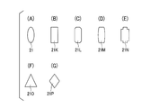
- each dot (dots 21A, 21B, 21C, 21D, 21E, 21F, 21G, etc.) constituting the light shielding layer 21 is an elongated oval shape.
- the shape of the light shielding layer 21 is not limited to this.
- an elongated rectangular light shielding layer 21K may be used.
- an elongated octagonal light shielding layer 21L may be used.
- a light shielding layer 21M having a shape in which two opposing sides of an elongated rectangle are curved outward may be used.
- the shape of the light shielding layer 21 is not limited to this.
- an elongated rectangular light shielding layer 21K may be used.
- an elongated octagonal light shielding layer 21L
- a light shielding layer 21N having a shape in which two rectangles having different aspect ratios intersect each other in two orthogonal directions may be used.
- an isosceles triangular light shielding layer 21O may be used.
- a diamond-shaped light shielding layer 21P may be used.
- planar shapes of the respective light shielding layers 21 are made different so that different types of sizes and shapes having various anisotropic orientations (see FIGS. 4A to 4G) are mixed. Also good.
- planar shape of the light shielding layer 21 as viewed from the normal direction of the one surface 20a of the base material 20 of the light diffusing member 15 is an isotropic shape
- the side surface shape of the light shielding layer 21 has a major axis and a minor axis. It may have an anisotropic shape.
- the direction in which the scattering intensity of the light diffusion member 15 is strong is a direction perpendicular to the longitudinal direction of the light shielding layer 21 (up and down direction on the paper surface) in FIG.
- the period (interval, pitch) in which the light shielding layers 21 are arranged is preferably smaller than the pixel pitches PP1 and PP2.
- the interval (pitch) from the dot 21A to the dot 21G and the interval (pitch) from the dot 21A to the dot 21H are preferably smaller than the pixel pitches PP1 and PP2.
- the pitch of moire interference fringes generated in the liquid crystal display device 10 the pixel pitch (pixel pitch PP1, pixel pitch PP2), and movement from the dot 21A to the closest dot 21B.
- the relationship between the angle formed by the direction DP1 will be described.
- the rubbing direction of the liquid crystal panel 13 is set to 45 degrees and 135 degrees, for example, the absorption axis direction (arrow ⁇ ′ direction) of the second polarizing plate 14 and the absorption axis of the first polarizing plate 12.
- the direction (arrow ⁇ ′ direction) is aligned with the rubbing direction.
- the arrow ⁇ ′ direction indicates the absorption axis direction of the first polarizing plate 12
- the arrow ⁇ ′ direction indicates the absorption axis direction of the second polarizing plate 14
- the arrow ⁇ ′ direction indicates the strong scattering direction of the liquid crystal panel 13.
- FIG. 6 when the light emitted from the backlight 11 spreads anisotropically, the light transmitted through the liquid crystal panel 13 is more liquid crystal than the vertical direction (90-270 degrees direction) of the liquid crystal panel 13.
- the display by the liquid crystal display device 10 is brightened in the horizontal direction perpendicular to the vertical direction of the liquid crystal panel 13 by spreading in the horizontal direction (0-180 degree direction) perpendicular to the vertical direction of the panel 13. Is possible.
- the strong scattering direction of the light diffusing member 15 is the vertical direction (90-270 degrees direction) of the liquid crystal panel 13, the light emitted from the backlight 11 is changed by using the light diffusing member 15. 13 can be strongly expanded in the vertical direction. Therefore, since the strong scattering direction is the vertical direction of the liquid crystal panel 13, the left and right light intensities have substantially the same light distribution characteristics, the appearance is symmetrical, and a wide viewing place can be realized.
- the strong scattering direction is the vertical direction of the liquid crystal panel 13
- light in the 90 degree direction and the 270 degree direction is likely to be mixed, and the anisotropy of the display characteristics of the liquid crystal panel 13 is alleviated, and the floor in the 270 degree direction. It is possible to improve tone reversal and color deviation from the front direction.
- the pitch of moire interference fringes generated in the liquid crystal display device 10 changes in period according to the rotation angle of the two diffraction gratings (the liquid crystal panel 13 and the light diffusing member 15), and the period becomes maximum when the two diffraction gratings are parallel.
- the period decreases as the angle formed by the repetitive periodic directions of the two diffraction gratings increases.
- the pitch of moire interference fringes is T M
- the repetition period of the liquid crystal panel 13 is T 1
- the repetition period of the light diffusion member 15 is T 2
- the angle formed by the liquid crystal panel 13 and the light diffusion member 15 is ⁇ 1 .
- pitch T M of the moire fringes is calculated by the following equation (1).
- a repetition period T 1 of the liquid crystal panel 13 a period that dots are formed in the pixel pitch PP1 direction, the repetition period T 2 of the light diffusing member 15, in the distance direction DP1 direction dot is formed It is a period.
- the moire interference fringes are not visually recognized. Therefore, when the direction of the pixel pitch PP1 or the direction of the pixel pitch PP2 of the liquid crystal panel 13 shown in FIG. 1B and the distance direction DP1 from the dot 21A to the closest dot 21G are parallel, The period of moire interference fringes generated by the distance direction DP1 and the direction of the pixel pitch PP1 is maximized, and the liquid crystal display device 10 is easily visible.
- the moire interference fringes generated by the distance direction DP1 and the direction of the pixel pitch PP1 or the direction of the pixel pitch PP2 The period can be reduced. Further, by making the distance direction DP2 and the direction of the pixel pitch PP1 or the direction of the pixel pitch PP2 non-parallel, the moire interference fringes generated by the distance direction DP2 and the direction of the pixel pitch PP1 or the direction of the pixel pitch PP2 The pitch (cycle) can be reduced. Thereby, the visibility of the liquid crystal display device 10 can be improved.
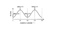
- FIG. 8 is a graph showing the relationship between the angle between the periodic structure with a period of 0.1 mm and the periodic structure with a period of 0.08 mm, and the pitch of moire interference fringes.
- the pitch of moire interference fringes decreases as the angle formed by the two periodic structures increases. That is, the visibility of the liquid crystal display device 10 can be improved as the angle between the distance directions DP1 and DP2 and the pixel pitches PP1 and PP2 increases.
- the dots of the light shielding layer 21 of the light diffusion member 15 arranged on the liquid crystal panel 13 are arranged in a hexagonal close-packed manner.
- the pixel pitch PP1 of the liquid crystal panel 13 is 0.033 mm
- the pixel pitch PP2 of the liquid crystal panel 13 is 0.099 mm.
- the angle formed by distance direction DP1-a and distance direction DP1-b is 60 degrees.
- the angle formed between the distance direction DP1-a and the distance direction DP2-a is 30 degrees.
- FIG. 10 is a graph showing the relationship between the angles formed by the distance directions DP1-a, DP1-b, DP1-c and the direction of the pixel pitch PP1 and the period of moire interference fringes generated in the liquid crystal display device 10.
- the period of the moire interference fringes is such that when the light diffusion member 15 is rotated, the angle formed by the distance directions DP1-a, DP1-b, DP1-c and the direction of the pixel pitch PP1 is every 60 degrees. It becomes the maximum.
- FIG. 11 shows moire interference fringes generated in the liquid crystal display device 10 and the angle formed by the distance directions DP1-a, DP1-b, DP1-c, DP2-a, DP2-b, DP2-c and the direction of the pixel pitch PP1. It is a graph which shows the relationship with this period.
- FIG. 12 shows the moire interference fringes generated in the liquid crystal display device 10 and the angles formed by the distance directions DP1-a, DP1-b, DP1-c, DP2-a, DP2-b, DP2-c and the pixel pitch PP2. It is a graph which shows the relationship with this period.
- the period is longer than the period of moire interference fringes formed by the angle between the distance directions DP1-a, DP1-b, DP1-c, DP2-a, DP2-b, DP2-c and the direction of the pixel pitch PP2. You can see that it also grows.
- the period of the moire interference fringes formed by the angle formed by the distance directions DP1-a, DP1-b, DP1-c, DP2-a, DP2-b, DP2-c and the direction of the pixel pitch PP1 is minimized.
- the moire interference fringes are least noticeable in the liquid crystal display device 10.
- the angle formed by the distance direction DP1-a and the direction of the pixel pitch PP1 is 10 degrees, 50 degrees, or 70 degrees, the moire interference fringes are least noticeable.
- the measuring method of the strong scattering direction of the light-diffusion member 15 is demonstrated.
- the normal line of the light diffusing member 15 is ⁇ 11 .
- the light diffusing member 15 is irradiated with the parallel light A from the light source 31.
- the normal line of the light diffusing member 15 angle (projection angle) of the (normal of one surface 20a of the substrate 20 constituting the light diffusing member) alpha 11 parallel light A and beta 11 .
- the parallel light A that has entered the light diffusing member 15 is scattered by the light diffusing member 15, and a part of the parallel light A is emitted to the light diffusing member 15 as the parallel light A ′ on the side opposite to the incident side of the parallel light A.
- the light receiver 32 receives the light.
- the angle (light receiving angle) of the normal line of the light diffusing member 15 alpha 11 parallel light A'and beta 12.
- the intensity of the parallel light A emitted from the light source 31 and the light projection angle ⁇ 11 and the light reception angle ⁇ 12 of the parallel light A ′ received by the light receiver 32 are fixed, and the light diffusing member 15 is changed to the normal ⁇ When 11 is rotated as the central axis, as shown in FIG.
- the light diffusing member 15 is an anisotropic light diffusing member in which the scattering intensity of the light diffusing portion 22 viewed from the normal direction has a strong scattering direction and a weak scattering direction.
- a measurement method in the repetitive periodic direction of the light shielding layer 21 will be described.
- an image of the light shielding layer 21 is taken in a range larger than the repetitive cycle of the light shielding layer 21 (the pitch between the light shielding layers 21) as shown in FIG.
- the image is subjected to two-dimensional Fourier transform, and as shown in FIG. 16, from the center of the diagram representing the power in shading, a bright spot direction with high power (a linear direction indicated by ⁇ 21 in FIG. 16) is repeatedly cycled. The direction.
- thermoplastic polymers such as thermoplastic polymers, thermosetting resins, and photopolymerizable resins are generally used.
- Made of appropriate transparent resin (light transmissive) made of acrylic polymer, olefin polymer, vinyl polymer, cellulose polymer, amide polymer, fluorine polymer, urethane polymer, silicon polymer, imide polymer, etc.
- a substrate can be used.
- the substrate 20 examples include triacetyl cellulose (TAC) film, polyethylene terephthalate (PET) film, cycloolefin polymer (COP) film, polycarbonate (PC) film, polyethylene naphthalate (PEN) film, polyethersulfone (A transparent resin substrate such as a PES) film or a polyimide (PI) film, a glass substrate, or the like is preferably used.
- TAC triacetyl cellulose
- PET polyethylene terephthalate
- COP cycloolefin polymer
- PC polycarbonate
- PEN polyethylene naphthalate
- PEN polyethylene naphthalate
- a transparent resin substrate such as a PES) film or a polyimide (PI) film, a glass substrate, or the like is preferably used.
- the thickness of the base material 20 is thin enough not to impair heat resistance and mechanical strength. The reason is that as the thickness of the base material 20 becomes thicker, there is a possibility that display blur may occur.
- the total light transmittance of the substrate 20 is preferably 90% or more as defined in JIS K7361-1. When the total light transmittance is 90% or more, sufficient transparency can be obtained.
- the light shielding layer 21 is made of, for example, an organic material having light absorption and photosensitivity such as a black resist.
- light shielding is achieved using metal films such as Cr (chromium) and Cr / Cr oxide multilayer films, pigments / dyes used for black ink, and multi-color inks to make black inks.
- the layer 21 may be formed.
- any material having a light shielding property can be used as the material of the light shielding layer 21.
- the light diffusion part 22 is formed by curing a negative photosensitive resin applied to one surface 20a of the substrate 20.
- the negative photosensitive resin include organic materials having optical transparency and photosensitivity such as acrylic resin and epoxy resin.
- the light scattering layer 23 is a layer in which a large number of light scattering bodies such as acrylic beads are dispersed inside a binder resin such as an acrylic resin on the other surface 20 b of the base material 20.
- the thickness of the light scattering layer 23 is, for example, about 0.5 to 20 ⁇ m. When the light scattering body is spherical, the diameter of the light scattering body is about 0.5 to 20 ⁇ m.
- the light scattering layer 23 is an isotropic diffusing material. The light scattering layer 23 isotropically diffuses the light diffused by the light diffusing unit 22 and further widens it.
- the light scatterer is not limited to acrylic beads, and is made of acrylic polymer, olefin polymer, vinyl polymer, cellulose polymer, amide polymer, fluorine polymer, urethane polymer, silicon polymer, imide polymer, or the like. You may be comprised with appropriate transparent substances, such as a resin piece, an inorganic type fine particle which consists of titanium oxide, a zinc oxide, etc., glass bead. In addition to these transparent substances, a scatterer or reflector that does not absorb light can be used as the light scatterer.
- the shape of each light scatterer can be formed in various shapes such as a spherical shape, an elliptical spherical shape, a flat plate shape, and a polygonal cube. It is only necessary that the size of the light scatterer is uniform or nonuniform.
- liquid crystal panel 13 an active matrix transmissive liquid crystal panel is illustrated as the liquid crystal panel 13, but a liquid crystal panel applicable to the present invention is not limited to an active matrix transmissive liquid crystal panel.
- the liquid crystal panel applicable to the present invention may be, for example, a transflective (transmissive / reflective) liquid crystal panel or a reflective liquid crystal panel.
- each pixel is a switching thin film transistor (Thin Film Transistor, hereinafter).
- TFT Thin Film Transistor
- FIG. 17 is a longitudinal sectional view of the liquid crystal panel 13.
- the liquid crystal panel 13 includes a TFT substrate 41 (corresponding to the TFT substrate 16 in FIG. 1) as a switching element substrate, and a color filter substrate 42 (in FIG. 1) arranged to face the TFT substrate 41. Equivalent to the color filter substrate 17) and a liquid crystal layer 43 sandwiched between the TFT substrate 41 and the color filter substrate.
- the liquid crystal layer 43 is surrounded by a TFT substrate 41, a color filter substrate 42, and a frame-shaped seal member (not shown) that bonds the TFT substrate 41 and the color filter substrate 42 at a predetermined interval. It is enclosed in the space.
- the liquid crystal panel 13 of the present embodiment performs, for example, a TN (Twisted Nematic) type display, and the liquid crystal layer 43 uses a vertically aligned liquid crystal having a negative dielectric anisotropy. Between the TFT substrate 41 and the color filter substrate 42, a spherical spacer 44 is disposed to keep the distance between the substrates constant.
- the display type is not limited to the TN type, but a VA (Vertical Alignment, Vertical Alignment) type, a STN (Super Twisted Nematic) type, an IPS (In-Plane Switching) type, or the like can be used.
- a plurality of pixels which are display minimum unit regions, are arranged in a matrix.
- a plurality of source bus lines (not shown) are formed on the TFT substrate 41 so as to extend in parallel with each other, and a plurality of gate bus lines (not shown) extend in parallel with each other, And it is formed so as to be orthogonal to a plurality of source bus lines. Therefore, on the TFT substrate 41, a plurality of source bus lines and a plurality of gate bus lines are formed in a lattice pattern, and a rectangular region partitioned by adjacent source bus lines and adjacent gate bus lines is one. One pixel.
- the source bus line is connected to the source electrode of the TFT described later, and the gate bus line is connected to the gate electrode of the TFT.
- a TFT 50 having a semiconductor layer 46, a gate electrode 47, a source electrode 48, a drain electrode 49, and the like is formed on the surface of the transparent substrate 45 constituting the TFT substrate 41 on the liquid crystal layer 43 side.
- a transparent substrate 45 for example, a glass substrate can be used.
- a semiconductor material such as CGS (Continuous Grain Silicon), LPS (Low-temperature Poly-Silicon), ⁇ -Si (Amorphous Silicon), etc.
- a semiconductor layer 46 is formed.
- a gate insulating film 51 is formed on the transparent substrate 45 so as to cover the semiconductor layer 46.
- the gate insulating film 51 for example, a silicon oxide film, a silicon nitride film, or a laminated film thereof is used.
- a gate electrode 47 is formed on the gate insulating film 51 so as to face the semiconductor layer 46.
- a laminated film of W (tungsten) / TaN (tantalum nitride), Mo (molybdenum), Ti (titanium), Al (aluminum), or the like is used.
- a first interlayer insulating film 52 is formed on the gate insulating film 51 so as to cover the gate electrode 47.
- a material of the first interlayer insulating film 52 for example, a silicon oxide film, a silicon nitride film, or a laminated film thereof is used.
- a source electrode 48 and a drain electrode 49 are formed on the first interlayer insulating film 52.
- the source electrode 48 is connected to the source region of the semiconductor layer 46 through a contact hole 53 that penetrates the first interlayer insulating film 52 and the gate insulating film 51.
- the drain electrode 49 is connected to the drain region of the semiconductor layer 46 through a contact hole 54 that penetrates the first interlayer insulating film 52 and the gate insulating film 51.
- the same conductive material as that of the gate electrode 47 described above is used.
- a second interlayer insulating film 55 is formed on the first interlayer insulating film 52 so as to cover the source electrode 48 and the drain electrode 49.
- the same material as the first interlayer insulating film 52 described above or an organic insulating material is used.
- a pixel electrode 56 is formed on the second interlayer insulating film 55.
- the pixel electrode 56 is connected to the drain electrode 49 through a contact hole 57 that penetrates the second interlayer insulating film 55. Therefore, the pixel electrode 56 is connected to the drain region of the semiconductor layer 46 using the drain electrode 49 as a relay electrode.
- a transparent conductive material such as ITO (Indium Tin Oxide) or IZO (Indium Zinc Oxide) is used.
- An alignment film 58 is formed on the entire surface of the second interlayer insulating film 55 so as to cover the pixel electrode 56.
- the alignment film 58 has an alignment regulating force that vertically aligns liquid crystal molecules constituting the liquid crystal layer 43.
- the form of the TFT may be the bottom gate TFT shown in FIG. 17 or the top gate TFT.
- a black matrix 60, a color filter 61, a planarizing layer 62, a counter electrode 63, and an alignment film 64 are sequentially formed on the surface of the transparent substrate 59 constituting the color filter substrate 42 on the liquid crystal layer 43 side.
- the black matrix 60 has a function of blocking the transmission of light in the inter-pixel region, and a metal such as a Cr (chromium) or Cr / Cr oxide multilayer film or carbon particles is dispersed in a photosensitive resin. It is formed of a photoresist.
- the color filter 61 includes red (R), green (G), and blue (B) dyes, and one pixel electrode 56 on the TFT substrate 41 has any one of R, G, and B.
- the planarization layer 62 is composed of an insulating film that covers the black matrix 60 and the color filter 61, and has a function of smoothing and leveling the step formed by the black matrix 60 and the color filter 61.
- a counter electrode 63 is formed on the planarization layer 62.
- As the material of the counter electrode 63 a transparent conductive material similar to that of the pixel electrode 56 is used.
- an alignment film 64 having a vertical alignment regulating force is formed on the entire surface of the counter electrode 63.
- the color filter 61 may have a multicolor configuration of three or more colors of R, G, and B.
- the backlight 11 includes a light source 71 such as a light emitting diode and a cold cathode tube, and a light guide that is emitted toward the liquid crystal panel 13 using internal reflection of light emitted from the light source 71. And an optical plate 72.
- the backlight 11 may be an edge light type in which a light source is disposed on an end face of a light guide, or may be a direct type in which a light source is disposed directly below the liquid crystal panel 13.
- a directional backlight that allows collimated or substantially collimated light to enter the light diffusing portion 23 of the light diffusing member 15
- blurring can be reduced and light utilization efficiency can be further increased.
- the directional backlight described above can be realized by optimizing the shape and arrangement of the reflection pattern formed in the light guide plate 72.
- a first polarizing plate 12 that functions as a polarizer is provided between the backlight 11 and the liquid crystal panel 13.
- a second polarizing plate 14 that functions as an analyzer is provided between the liquid crystal panel 13 and the light diffusion member 15.
- the case where the second polarizing plate 14 is provided between the base material 20 of the light diffusing member 15 and the liquid crystal panel 13 is exemplified.
- a member having a refractive index between the refractive index of the substrate 20 and the refractive index of the second polarizing plate 14 may be interposed therebetween.
- the liquid crystal panel 13 is a TN type in which the light distribution characteristics do not have azimuth symmetry. Further, the direction of strong anisotropy of the liquid crystal panel 13 and the strong scattering direction of the light diffusion member 15 are substantially parallel.
- FIG. 18 is a flowchart showing a method for manufacturing the light diffusing member 15.
- FIGS. 19A to 19E are perspective views showing the manufacturing process of the light diffusing member 15 step by step.
- the manufacturing method of the liquid crystal display device 10 will be described focusing on the manufacturing steps of the light diffusing member 15 constituting the liquid crystal display device 10 having the above-described configuration.
- the outline of the manufacturing process of the liquid crystal panel 13 will be described first. First, the TFT substrate 41 and the color filter substrate 42 shown in FIG. Thereafter, the surface of the TFT substrate 41 on which the TFT 50 is formed and the surface of the color filter substrate 42 on which the color filter 61 is formed are arranged to face each other.
- the TFT substrate 41 and the color filter substrate 42 are bonded together via a seal member. Thereafter, liquid crystal is injected into a space surrounded by the TFT substrate 41, the color filter substrate 42, and the seal member.
- the liquid crystal panel 13 is completed through the above steps.
- the first polarizing plate 12 is bonded to the outer surface of the liquid crystal panel 13 thus manufactured on the TFT substrate 41 side using an optical adhesive or the like. Note that the manufacturing method of the TFT substrate 41 and the color filter substrate 42 may be a conventional method, and the description thereof is omitted.
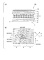
- the manufacturing process of the light diffusing member 15 will be described. As shown in FIGS. 19A to 19E, the light diffusing member 15 is formed in this order by a manufacturing apparatus including a printing apparatus 90, a coating apparatus 95, an exposure apparatus 100, a developing apparatus 105, and a polarizing plate pasting apparatus 110. Manufactured by various treatments.
- the printing apparatus 90 conveys a long base material 80 by roll-to-roll, and performs a printing process during that time.
- a feed roller 91 that feeds the substrate 80 is provided at one end, and a take-up roller 92 that winds the substrate 80 is provided at the other end.
- the base material 80 is configured to move from the delivery roller 91 side toward the take-up roller 92 side.
- a printing roller 93 is provided above the substrate 80.
- the coating device 95 transports the base material 80 that has been subjected to the printing process by roll-to-roll, and performs the coating process during that time.
- a feed roller 96 for feeding the substrate 80 is provided at one end, and a take-up roller 97 for winding the substrate 80 is provided at the other end.
- the base material 80 is configured to move from the delivery roller 96 side toward the take-up roller 97 side.
- a slit coater 98 is provided above the substrate 80.
- the exposure apparatus 100 transports the base material 80 that has been subjected to the coating process in a roll-to-roll manner, and performs the exposure process during that time.
- a feed roller 101 that feeds the substrate 80 is provided at one end, and a take-up roller 102 that winds the substrate 80 is provided at the other end.
- the base material 80 is configured to move from the delivery roller 101 side toward the take-up roller 102 side.
- a light source (not shown) that emits the diffused light Q1 is provided below the substrate 80.
- the developing device 105 conveys the base material 80 that has been subjected to the exposure process in a roll-to-roll manner, and performs the development process therebetween.
- a feed roller 106 that feeds the substrate 80 is provided at one end, and a take-up roller 107 that winds the substrate 80 is provided at the other end.
- the base material 80 is configured to move from the delivery roller 106 side toward the take-up roller 107 side.
- a device (not shown) for discharging the developer Q2 is provided above the base material 80.
- the polarizing plate pasting apparatus 110 conveys the base material 80 (base material of the light diffusing member) that has been subjected to the development process by roll-to-roll, and the polarizing plate pasting process between them. (A process of attaching the base material of the second polarizing plate).
- a first feed roller 111 that feeds the base material 80 is provided at one end, and a winding roller 112 that winds up the base material subjected to the polarizing plate sticking process is provided at the other end.
- the base material 80 is configured to move from the delivery roller 111 side toward the take-up roller 112 side.
- a second delivery roller 113 that feeds the base material of the second polarizing plate is provided above the base material 80.
- a pair of sticking rollers 114 and 115 for sticking the base material of the light diffusing member and the base material of the second polarizing plate are provided in the conveyance path of the base material 80.
- the long base material 80 for example, a base material made of triacetyl cellulose is prepared.
- a printing apparatus 90 shown in FIG. 19A a light-shielding layer 81 made of black resin or black ink containing carbon as a light-shielding layer material on one surface 80a of the base material 80 is applied to a printing roller 93.
- the planar shape of the light shielding layer 81 is elliptical.
- the printing apparatus 90 performs printing so that the repetition period of the light shielding layer 81 (the light shielding layer 21) and the strong scattering direction of the light diffusion member 15 are not parallel.
- the printing is performed so that the major axis direction of the light shielding layer 81 is inclined by approximately 45 degrees or 135 degrees with respect to the length direction of the substrate 80 (the conveyance direction of the substrate 80).
- printing methods such as gravure printing, offset printing, and gravure offset printing are used.
- the some light shielding layer 21 is formed in the one surface 80a of the base material 80 (step S1 shown in FIG. 18).
- the oval light shielding layer 81 corresponds to a non-formation region (hollow portion 83) of the light diffusion portion 82 in the next step.
- the arrangement of the interval (pitch) between the adjacent light shielding layers 81 has a repetition period. It is desirable that the interval (pitch) of the light shielding layers 81 is smaller than the interval (pitch) of the pixels of the liquid crystal panel 13. Thereby, at least one light shielding layer 81 (light shielding layer 21) is formed in the pixel. Therefore, for example, a wide viewing angle can be achieved when combined with a liquid crystal panel having a small pixel pitch used for a mobile device or the like.
- the light shielding layer 81 was formed using the printing method, this embodiment is not limited to this.
- the light shielding layer 81 can also be formed by a photolithography method using a black negative resist. In this case, if a photomask in which the opening pattern and the light shielding pattern are reversed is used, a positive resist having a light absorption property can also be used.
- the light shielding layer 81 may be directly formed by using a vapor deposition method, screen printing, an ink jet method, or the like.
- an acrylic resin is used as a light diffusing portion material so as to cover a plurality of light shielding layers 81 on one surface 80a of the substrate 80. Apply a transparent negative resist. Thereby, the coating film (negative photosensitive resin layer) 84 is formed (step S2 shown in FIG. 18).
- the transparent negative resist is formed using a slit coater, but the present embodiment is not limited to this.
- the transparent negative resist may be formed using a spin coating method, a printing method, or the like.
- the coating film 84 is irradiated with the diffused light Q1 using the plurality of light-shielding layers 81 having an elliptical planar shape as a mask to perform exposure (step S3 shown in FIG. 18).
- an exposure apparatus using a mixed line of i-line having a wavelength of 365 nm, h-line having a wavelength of 404 nm, and g-line having a wavelength of 436 nm is used.
- the exposure amount is 500 mJ / cm 2 .
- the coating film 84 made of a transparent negative resist is developed using a dedicated developer Q2, and post-baked at 100 ° C. to have a plurality of hollow portions 83.
- the light diffusion portion 81 is formed on one surface 80a of the base material 80 (step S4 shown in FIG. 18).
- the transparent negative resist constituting the coating film 84 spreads outward from the non-formation region of the light shielding layer 81. Are exposed radially. Thereby, the forward tapered hollow portion 83 is formed.
- the light diffusion part 82 (light diffusion part 22 shown in FIGS. 1 and 2) has an inversely tapered shape. The inclination angle of the side surface (reflection surface) of the light diffusion portion 82 can be controlled by the degree of diffusion of the diffused light.
- the light Q1 used here parallel light, diffused light, or light whose intensity at a specific emission angle is different from the intensity at other emission angles, that is, light having intensity at a specific emission angle can be used.
- the inclination angle of the reflection surface of the light diffusing unit 82 becomes a single inclination angle of about 60 ° to 90 °, for example.
- the tilt angle changes continuously, and the cross-sectional shape becomes a curved inclined surface.
- an inclined surface having an inclination angle corresponding to the intensity is obtained. In this way, the inclination angle of the reflection surface of the light diffusion portion 82 can be adjusted.
- the exposure apparatus 100 and an optical path of the light emitted from the exposure apparatus 100 are arranged. And a combination of a diffusion plate having a haze of about 50. With this combination, light emitted from the exposure apparatus 100 can be irradiated through the diffusion plate.
- the total light transmittance of the light diffusing member 15 is preferably 90% or more. When the total light transmittance is 90% or more, sufficient transparency can be obtained, and the optical performance required for the light diffusion member 15 can be sufficiently exhibited.
- the total light transmittance is as defined in JIS K7361-1.
- the base material 85 of the second polarizing plate 14 is applied to the light incident end face 22b of the light diffusion portion 22 in the base material of the light diffusing member 15, and the adhesive layer is applied. (Step S5 shown in FIG. 18).
- the light-diffusion member 15 corresponding to the planar view size of the liquid crystal display device 10 is individualized by cut
- the light diffusing member 15 is separated into pieces so that the strong scattering direction Vs of the light diffusing member 15 and one side of the second polarizing plate 14 are parallel to each other. For example, as shown in FIG.
- the bonded body 86 includes an azimuth angle direction Vs in which the base material of the light diffusing member 15 is relatively strong, and a short side that forms the outer shape of the light diffusing member 15 after being singulated. Are cut along the virtual cutting line CL so that they are substantially parallel (match).
- the light diffusion member 15 is completed through the above steps.
- the completed light diffusion member 15 is used with an optical adhesive or the like with the base material 20 facing the viewing side and the second polarizing plate 14 facing the liquid crystal panel 13. Affixed to the liquid crystal panel 13.
- the liquid crystal display device 10 according to the present embodiment is obtained.
- the periodic direction in which the light shielding layer 21 is repeatedly formed and the pixel pitch direction of the liquid crystal panel 13 are not parallel.
- the light diffusing member 15 is obtained by cutting the bonded body 86 on which the base material of the light diffusing member 15 and the base material 85 of the second polarizing plate 14 are bonded to the size of the liquid crystal display device 10 in plan view.
- the present embodiment is not limited to this.
- the light shielding layer 21 is repeatedly formed after the base material of the light diffusing member 15 and the base material 85 of the second polarizing plate 14 are cut into the size of the liquid crystal display device 10 in plan view.
- the light diffusing member 15 and the second polarizing plate 14 may be pasted so that the periodic direction and the pixel pitch direction of the liquid crystal panel 13 are non-parallel.
- the liquid crystal display device 10 was formed by affixing on the liquid crystal panel 13, This embodiment is not limited to this.
- the base material of the light diffusing member 15 is cut into a planar view size of the liquid crystal display device 10 to obtain the light diffusing member 15.
- the light diffusing member 15 may be attached to the liquid crystal panel 13 to which the second polarizing plate 14 has been previously attached to manufacture the liquid crystal display device 10.
- the light-diffusion member 15 is the base material 20 which has a light transmittance, the some light shielding layer 21 formed in the one surface 20a of the base material 20, and the one surface 20a of the base material 20.
- the present embodiment is not limited to this case.
- the present embodiment is not limited to this example.
- the light diffusing member 15 includes a base material 20 having light permeability, a plurality of light diffusing portions 22 formed on one surface 20a of the base material 20 with a repeating cycle,
- One surface 20a of the material 20 may include a light shielding layer 21 formed in a region other than the region where the light diffusion portion 22 is formed.
- the light shielding layer 21 having an opening with a repeating cycle is formed on one surface 20 a of the base material 20, and the light shielding layer is formed on the one surface 20 a of the base material 20.
- a light-sensitive negative photosensitive resin layer is formed so as to cover the light-shielding layer 21, and the light-shielding layer is formed from the surface opposite to the one surface 20 a of the base material 20 on which the light-shielding layer 21 and the negative photosensitive resin layer are formed.
- the negative photosensitive resin layer is irradiated with diffused light through the opening 21, the negative photosensitive resin layer is exposed, the exposed negative photosensitive resin layer is developed, and the light diffusing portion 22 is developed. You may form in the one surface 20a side of the material 20. FIG.
- FIGS. 21 and 22 An example of a liquid crystal display device including a transmissive liquid crystal display element as a display device will be described.
- the scale of the size may be changed depending on the component.
- FIG. 21 the same components as those shown in FIG. 1 are denoted by the same reference numerals, and the description thereof is omitted.
- FIG. 22 the same components as those shown in FIG. 2 are denoted by the same reference numerals, and the description thereof is omitted.
- FIG. 21 is a schematic diagram illustrating the liquid crystal display device of the present embodiment, in which (A) is a cross-sectional view of the liquid crystal display device of the present embodiment, and (B) is a plan view of the liquid crystal display device of the present embodiment.
- FIG. 22 is a cross-sectional view of the light diffusing member of this embodiment.
- a liquid crystal display device (display device) 120 according to the present embodiment is schematically configured from a backlight (light source) 11, a first polarizing plate 12, a liquid crystal panel 13, a second polarizing plate 14, and a light diffusion member 121. ing.
- the light diffusing member 121 includes a light-transmitting base material 20, a plurality of light shielding layers 122 formed on one surface 20 a of the base material 20, and a region where the light shielding layer 122 is formed on the one surface 20 a of the base material 20.
- region other than and the light-scattering layer 23 formed in the other surface (surface on the visual recognition side) 20b of the base material 20 are comprised roughly.
- the liquid crystal panel 13 is a TN type in which the light distribution characteristics do not have azimuth symmetry. Further, the strongly anisotropic direction of the liquid crystal panel 13 and the strong scattering direction of the light diffusion member 121 are substantially parallel.
- the planar shape of the light shielding layer 122 viewed from the normal direction of the other surface 20b of the substrate 20 has at least a major axis and a minor axis. It has an anisotropic shape (elongated elliptical shape).
- the light shielding layer 122 is arranged with a predetermined period. For example, as shown in FIG. 21B, four dots 122B of the light shielding layer 122 are arranged around one dot 122A of the light shielding layer 122 as a center. , 122C, 122D, 122E are arranged in four rotational symmetry.
- the periodic direction in which the light shielding layer 122, that is, the dots 122A, 122B, 122C, 122D, and 122E constituting the light shielding layer 122 are repeatedly formed and the pixel pitch direction of the liquid crystal panel 13 are not parallel. It has become.
- the pixel pitch of the liquid crystal panel 13 is PP1 that is the interval between the red (R), green (G), and blue (B) colorants, and the width of each colorant. It is PP2 that is.
- 122B, 122C, 122D, and 122E are arranged in a substantially square shape. At this time, as shown in FIG.
- the distance (pitch) direction DP11 is not parallel. Further, the direction of the pixel pitch PP1 and the direction of the pixel pitch PP2 are not parallel to the distance (pitch) direction DP12 from the dot 122A to the dot 122E which is one of the dots closest to the dot 122A. ing.
- each dot (dots 122A, 122B, 122C, 122D, 122E, etc.) constituting the light shielding layer 122 is not limited to an elongated elliptical shape, but is an elongated rectangular shape or an elongated octagonal shape as shown in FIG.
- the shape may be a shape in which two opposing sides of an elongated rectangle are curved outward, a shape in which two rectangles having different aspect ratios intersect each other in two orthogonal directions, an isosceles triangle shape, a rhombus shape, or the like.
- each light shielding layer 122 may be different, and a plurality of different sizes and shapes having various anisotropic orientations may be mixed. Further, the planar shape of the light shielding layer 122 viewed from the normal direction of the one surface 20a of the base material 20 of the light diffusing member 121 is an isotropic shape, and the side surface shape of the light shielding layer 122 has a major axis and a minor axis. It may have an anisotropic shape.
- the period (interval, pitch) in which the light shielding layers 122 are arranged is preferably smaller than the pixel pitches PP1 and PP2.
- the interval (pitch) from the dot 122A to the dot 122B and the interval (pitch) from the dot 122A to the dot 122E are preferably smaller than the pixel pitches PP1 and PP2.
- the direction of the pixel pitch PP1 and the direction of the pixel pitch PP2 and the interval (pitch) direction DP11 from the dot 122A to the dot 122B are nonparallel
- the direction of the pixel pitch PP1 and the direction of the pixel pitch PP2 Since the direction and the interval (pitch) direction DP12 from the dot 122A to the dot 122E are non-parallel, moire interference fringes are not noticeable in the liquid crystal display device 120, and the visibility of the liquid crystal display device 120 can be improved. .
- the angle range in which moire interference fringes can be reduced is widened.
- the light diffusing member 121 includes the base material 20 having light transmittance, the plurality of light shielding layers 122 formed on the one surface 20a of the base material 20, and the one surface 20a of the base material 20.
- the present embodiment is not limited to this example.
- the present embodiment is not limited to this.
- the light diffusing member 121 includes a base material 20 having light permeability, a plurality of light diffusing portions 22 formed on one surface 20a of the base material 20 with a repeating cycle,
- One surface 20a of the material 20 may include a light shielding layer 122 formed in a region other than the region where the light diffusion portion 22 is formed.
- the light shielding layer 21 having an opening with a repeating cycle is formed on one surface 20 a of the base material 20, and the light shielding layer is formed on the one surface 20 a of the base material 20.
- a light-sensitive negative photosensitive resin layer is formed so as to cover the light-shielding layer 21, and the light-shielding layer is formed from the surface opposite to the one surface 20 a of the base material 20 on which the light-shielding layer 21 and the negative photosensitive resin layer are formed.
- the negative photosensitive resin layer is irradiated with diffused light through the opening 21, the negative photosensitive resin layer is exposed, the exposed negative photosensitive resin layer is developed, and the light diffusing portion 22 is developed. You may form in the one surface 20a side of the material 20. FIG.
- FIG. 23 is a schematic diagram illustrating the liquid crystal display device of the present embodiment, where FIG. 23A is a cross-sectional view of the liquid crystal display device of the present embodiment, and FIG. 23B is a plan view of the liquid crystal display device of the present embodiment.
- FIG. 24 is a cross-sectional view of the light diffusing member of this embodiment.
- a liquid crystal display device (display device) 130 according to the present embodiment is generally configured by a backlight (light source) 11, a first polarizing plate 12, a liquid crystal panel 13, a second polarizing plate 14, and a light diffusion member 131. ing.
- the light diffusing member 131 includes a light-transmitting base material 20, a plurality of light shielding layers 132 formed on one surface 20 a of the base material 20, and a region where the light shielding layer 132 is formed on the one surface 20 a of the base material 20.
- region other than and the light-scattering layer 23 formed in the other surface (surface on the visual recognition side) 20b of the base material 20 are comprised roughly.
- the liquid crystal panel 13 is a TN type in which the light distribution characteristics do not have azimuth symmetry. Further, the direction of strong anisotropy of the liquid crystal panel 13 and the direction of strong scattering of the light diffusion member 131 are substantially parallel.
- the planar shape of the light shielding layer 132 viewed from the normal direction of the other surface 20b of the substrate 20 has at least a major axis and a minor axis. It has an anisotropic shape (elongated elliptical shape).
- the light shielding layer 132 is arranged with a predetermined period. For example, as shown in FIG. 23B, the four dots 132B of the light shielding layer 132 are provided around one dot 132A of the light shielding layer 132 as a center. , 132C, 132D, 132E are arranged in two rotational symmetry.
- the periodic direction in which the light shielding layer 132, that is, the dots 132A, 132B, 132C, 132D, 132E and the like constituting the light shielding layer 132 are repeatedly formed and the pixel pitch direction of the liquid crystal panel 13 are not parallel. It has become.
- the pixel pitch of the liquid crystal panel 13 refers to PP1 which is the interval between the red (R), green (G), and blue (B) dyes, and the width of each dye. It is PP2 that is.
- the dots 132B, 132C, 132D, and 132E are arranged in a substantially rhombus shape. At this time, as shown in FIG.
- the direction of the pixel pitch PP1 and the direction of the pixel pitch PP2 and the distance (pitch) direction DP22 from the dot 132A to the dot 132B closest to the dot 132A Are non-parallel. Further, the direction of the pixel pitch PP1 and the direction of the pixel pitch PP2 are not parallel to the distance (pitch) direction DP21 from the dot 132A to the dot 132E that is second closest thereto.
- each dot (dots 132A, 132B, 132C, 132D, 132E, etc.) constituting the light-shielding layer 132 is not limited to an elongated elliptical shape, but is an elongated rectangular shape or an elongated octagonal shape as shown in FIG.
- the shape may be a shape in which two opposing sides of an elongated rectangle are curved outward, a shape in which two rectangles having different aspect ratios intersect each other in two orthogonal directions, an isosceles triangle shape, a rhombus shape, or the like.
- each light shielding layer 132 may be different, and a plurality of different types of sizes and shapes having various anisotropic orientations may be mixed. Further, the planar shape of the light shielding layer 132 viewed from the normal direction of the one surface 20a of the base material 20 of the light diffusing member 131 is an isotropic shape, and the side surface shape of the light shielding layer 132 has a major axis and a minor axis. It may have an anisotropic shape.
- the period (interval, pitch) in which the light shielding layers 132 are arranged is preferably smaller than the pixel pitches PP1 and PP2.
- the interval (pitch) from the dot 132A to the dot 132B and the interval (pitch) from the dot 132A to the dot 132E are preferably smaller than the pixel pitches PP1 and PP2.
- the direction of the pixel pitch PP1 and the direction of the pixel pitch PP2 and the interval (pitch) direction DP22 from the dot 132A to the dot 132B are nonparallel
- the direction of the pixel pitch PP1 and the direction of the pixel pitch PP2 Since the direction and the interval (pitch) direction DP21 from the dot 132A to the dot 132E are non-parallel, the moire interference fringes are not noticeable in the liquid crystal display device 130, and the visibility of the liquid crystal display device 130 can be improved.
- the four dots 132B, 132C, 132D, and 132E of the light shielding layer 132 are arranged in two-fold rotational symmetry, so the angle range in which moire interference fringes can be reduced is widened.
- the light diffusing member 131 includes the base material 20 having light transmittance, the plurality of light shielding layers 132 formed on the one surface 20a of the base material 20, and the one surface 20a of the base material 20.
- the present embodiment is not limited to this, although the light diffusing portion 22 formed in the region other than the region where the light shielding layer 132 is formed is illustrated.
- the light diffusing member 131 includes a base material 20 having light transmittance, a plurality of light diffusing portions 22 formed on one surface 20a of the base material 20 with a repeating cycle,
- One surface 20a of the material 20 may include a light shielding layer 132 formed in a region other than the region where the light diffusion portion 22 is formed.
- the light shielding layer 21 having an opening with a repeating cycle is formed on one surface 20 a of the base material 20, and the light shielding layer is formed on the one surface 20 a of the base material 20.
- a light-sensitive negative photosensitive resin layer is formed so as to cover the light-shielding layer 21, and the light-shielding layer is formed from the surface opposite to the one surface 20 a of the base material 20 on which the light-shielding layer 21 and the negative photosensitive resin layer are formed.
- the negative photosensitive resin layer is irradiated with diffused light through the opening 21, the negative photosensitive resin layer is exposed, the exposed negative photosensitive resin layer is developed, and the light diffusing portion 22 is developed. You may form in the one surface 20a side of the material 20. FIG.
- FIG. 25 an example of a liquid crystal display device including a transmissive liquid crystal display element as a display device will be described.
- the scale of the size may be changed depending on the component. 25
- the same components as those shown in FIG. 1 are denoted by the same reference numerals, and the description thereof is omitted.
- FIG. 26 the same components as those shown in FIG. 2 are denoted by the same reference numerals, and the description thereof is omitted.
- FIGS. 25A and 25B are schematic views showing the liquid crystal display device of the present embodiment, where FIG. 25A is a cross-sectional view of the liquid crystal display device of the present embodiment, and FIGS. 25B and C are plan views of the liquid crystal display device of the present embodiment.
- FIG. FIG. 26 is a cross-sectional view of the light diffusing member of this embodiment.
- a liquid crystal display device (display device) 140 according to the present embodiment is roughly configured by a backlight (light source) 11, a first polarizing plate 12, a liquid crystal panel 13, a second polarizing plate 14, and a light diffusion member 141. ing.
- the light diffusing member 141 includes a light-transmitting base material 20, a plurality of light shielding layers 142 formed on one surface 20 a of the base material 20, and a region where the light shielding layer 142 is formed on the one surface 20 a of the base material 20.
- region other than and the light-scattering layer 23 formed in the other surface (surface on the visual recognition side) 20b of the base material 20 are comprised roughly.
- the liquid crystal panel 13 is a TN type in which the light distribution characteristics do not have azimuth symmetry. Further, the direction of strong anisotropy of the liquid crystal panel 13 and the direction of strong scattering of the light diffusing member 141 are substantially parallel.
- the planar shape of the light shielding layer 142 viewed from the normal direction of the other surface 20b of the substrate 20 has at least a major axis and a minor axis. It has an anisotropic shape (elongated elliptical shape).
- the light shielding layers 142 are arranged randomly when viewed microscopically, but a plurality of the light shielding layers 142 arranged at random gather together to form one group, The group is arranged with a predetermined period.
- the dots 142A to 142T of the light shielding layer 142 are randomly arranged.
- the plurality of dots 142A to 142T gather to form one group 143, and the group 143 is arranged with a predetermined period.
- a periodic direction in which a group 143 composed of a plurality of randomly arranged dots 142A to 142T is repeatedly formed (interval direction between groups composed of a plurality of dots) and a pixel pitch of the liquid crystal panel 13
- the direction is non-parallel.
- the pixel pitch of the liquid crystal panel 13 refers to PP1 that is the interval between the red (R), green (G), and blue (B) dyes, and the width of each dye. It is PP2 that is.
- the group 143 forms a substantially rectangular region. At this time, as shown in FIGS.
- the direction of the pixel pitch PP1 and the direction of the pixel pitch PP2, and the length direction AP1 of the long side of the rectangular region forming the group 143 are non-parallel.
- the direction of the pixel pitch PP1 and the direction of the pixel pitch PP2 are not parallel to the length direction AP2 of the diagonal line of the rectangular area forming the group 143.
- the interval between the groups 143 formed of the plurality of dots 142A to 142T is such that when the group 143 forms a substantially rectangular region, the length of the long side or the short side of the rectangular region, or It is represented by the length of the diagonal line of the rectangular area.
- each dot (dots 142A to 142T, etc.) constituting the light shielding layer 142 is not limited to an elongated oval shape, and as shown in FIG. 4, an elongated rectangular shape, an elongated octagonal shape, and an elongated rectangular shape face each other.
- the shape may be a shape in which two sides are curved outward, a shape in which two rectangles having different aspect ratios are intersected in two orthogonal directions, an isosceles triangle shape, a rhombus shape, or the like.
- the planar shape of each light shielding layer 142 may be different, and a plurality of different types of sizes and shapes having various anisotropic orientations may be mixed.
- planar shape of the light shielding layer 142 viewed from the normal direction of the one surface 20a of the base material 20 of the light diffusing member 141 is an isotropic shape
- the side surface shape of the light shielding layer 142 has a major axis and a minor axis. It may have an anisotropic shape.
- the interval (pitch) at which the light shielding layers 142 are arranged is preferably smaller than the pixel pitches PP1 and PP2. Specifically, the interval (pitch) from the dot 142A to the dot 142B and the interval (pitch) from the dot 142A to the dot 142E are preferably smaller than the pixel pitches PP1 and PP2. Thereby, at least one light shielding layer 142 is formed in the pixel.
- the direction of the pixel pitch PP1 and the direction of the pixel pitch PP2, and the length direction of the long side of the rectangular region forming the group 143 composed of the plurality of dots 142A to 142T constituting the light shielding layer 142 AP1 is non-parallel
- AP2 is nonparallel, the moire interference fringes are not noticeable in the liquid crystal display device 140, and the visibility of the liquid crystal display device 140 can be improved.
- a plurality of dots 142A to 142T are gathered to form one group 143, and the group 143 is arranged with a predetermined period. Therefore, design data for producing the light shielding layer 142 is provided. The size can be reduced.
- the light diffusing member 141 includes the light-transmitting base material 20, the plurality of light shielding layers 142 formed on the one surface 20 a of the base material 20, and the one surface 20 a of the base material 20.
- the present embodiment is not limited to this, although the light diffusing portion 22 formed in the region other than the region where the light shielding layer 142 is formed is illustrated.
- the light diffusing member 141 includes a light-transmitting base material 20, a plurality of light diffusing portions 22 formed on one surface 20 a of the base material 20 with a repeating cycle, and a base One surface 20a of the material 20 may include a light shielding layer 142 formed in a region other than the region where the light diffusion portion 22 is formed.
- the light shielding layer 21 having an opening with a repeating cycle is formed on one surface 20 a of the base material 20, and the light shielding layer is formed on the one surface 20 a of the base material 20.
- a light-sensitive negative photosensitive resin layer is formed so as to cover the light-shielding layer 21, and the light-shielding layer is formed from the surface opposite to the one surface 20 a of the base material 20 on which the light-shielding layer 21 and the negative photosensitive resin layer are formed.
- the negative photosensitive resin layer is irradiated with diffused light through the opening 21, the negative photosensitive resin layer is exposed, the exposed negative photosensitive resin layer is developed, and the light diffusing portion 22 is developed. You may form in the one surface 20a side of the material 20. FIG.
- FIGS. 1-10 Fifth Embodiment
- a fifth embodiment of the present invention will be described with reference to FIGS.
- a liquid crystal display device including a transmissive liquid crystal display element as a display device will be described.
- the scale of the size may be changed depending on the component.
- FIG. 27 the same components as those shown in FIG. In FIG. 28, the same components as those shown in FIG. 2 are denoted by the same reference numerals, and the description thereof is omitted.
- FIG. 27 is a schematic view showing the liquid crystal display device of the present embodiment, in which (A) is a cross-sectional view of the liquid crystal display device of the present embodiment, and (B) and (C) are plan views of the liquid crystal display device of the present embodiment.
- FIG. FIG. 28 is a cross-sectional view of the light diffusing member of this embodiment.
- a liquid crystal display device (display device) 150 according to the present embodiment is schematically configured from a backlight (light source) 11, a first polarizing plate 12, a liquid crystal panel 13, a second polarizing plate 14, and a light diffusion member 151. ing.
- the light diffusing member 151 includes a light-transmitting base material 20, a plurality of light shielding layers 152 formed on one surface 20 a of the base material 20, and a region where the light shielding layer 152 is formed on the one surface 20 a of the base material 20.
- region other than and the light-scattering layer 23 formed in the other surface (surface on the visual recognition side) 20b of the base material 20 are comprised roughly.
- the liquid crystal panel 13 is a TN type in which the light distribution characteristics do not have azimuth symmetry. Further, the direction of strong anisotropy of the liquid crystal panel 13 and the strong scattering direction of the light diffusion member 151 are substantially parallel.
- the planar shape of the light shielding layer 152 viewed from the normal direction of the other surface 20b of the substrate 20 has at least a major axis and a minor axis. It has an anisotropic shape (elongated elliptical shape).
- the light shielding layers 152 are arranged randomly when viewed microscopically, but a plurality of the light shielding layers 152 arranged at random gather to form one group, The group is arranged with a predetermined period.
- the dots 152A to 152S of the light shielding layer 152 are randomly arranged.
- the plurality of dots 152A to 152S gather to form one group 153, and the group 153 is arranged with a predetermined period.
- a periodic direction in which a group 153 composed of a plurality of randomly arranged dots 152A to 152S is repeatedly formed (interval direction between groups composed of a plurality of dots) and a pixel pitch of the liquid crystal panel 13
- the direction is non-parallel.
- the pixel pitch of the liquid crystal panel 13 refers to PP1 which is the interval between the red (R), green (G), and blue (B) dyes, and the width of each dye. It is PP2 that is.
- the group 153 forms a substantially square region. At this time, as shown in FIGS.
- the direction of the pixel pitch PP1 and the direction of the pixel pitch PP2 and the length direction AP11 of one side of the square region forming the group 153 are It is non-parallel. Further, the direction of the pixel pitch PP1 and the direction of the pixel pitch PP2 are not parallel to the length direction AP12 of the diagonal line of the square region forming the group 153. Note that the interval between the groups 153 formed of the plurality of dots 152A to 152S is such that when the group 153 forms a substantially square region, the length of one side of the square region, or the square shape It is represented by the length of the diagonal of the area.
- each dot (dots 152A to 152S, etc.) constituting the light shielding layer 152 is not limited to an elongated oval shape, and as shown in FIG.
- the shape may be a shape in which two sides are curved outward, a shape in which two rectangles having different aspect ratios are intersected in two orthogonal directions, an isosceles triangle shape, a rhombus shape, or the like.
- the planar shape of each light shielding layer 152 may be different, and a plurality of different types of sizes and shapes having various anisotropic orientations may be mixed.
- planar shape of the light shielding layer 152 viewed from the normal direction of the one surface 20a of the base material 20 of the light diffusing member 151 is an isotropic shape
- the side surface shape of the light shielding layer 152 has a major axis and a minor axis. It may have an anisotropic shape.
- the interval (pitch) at which the light shielding layers 152 are arranged is preferably smaller than the pixel pitches PP1 and PP2. Specifically, the interval (pitch) from the dot 152A to the dot 152B and the interval (pitch) from the dot 152A to the dot 152E are preferably smaller than the pixel pitches PP1 and PP2. Thereby, at least one light shielding layer 152 is formed in the pixel.
- the direction of the pixel pitch PP1 and the direction of the pixel pitch PP2, and the length direction AP11 of one side of the square area forming the group 153 composed of the plurality of dots 152A to 152S constituting the light shielding layer 152 Are non-parallel, the direction of the pixel pitch PP1 and the direction of the pixel pitch PP2, and the diagonal length direction AP12 of the rectangular region forming the group 153 composed of the plurality of dots 152A to 152S constituting the light shielding layer 152 And non-parallel to each other, the moire interference fringes are not noticeable in the liquid crystal display device 150, and the visibility of the liquid crystal display device 150 can be improved.
- a plurality of dots 152A to 152S are gathered to form one group 153, and the group 153 is arranged with a predetermined period. Therefore, design data for producing the light shielding layer 152 is provided. The size can be reduced.
- the light diffusing member 151 includes the light-transmitting base material 20, the plurality of light shielding layers 152 formed on the one surface 20 a of the base material 20, and the one surface 20 a of the base material 20.
- the present embodiment is not limited to this case.
- the present embodiment is not limited to this.
- the light diffusing member 151 includes a base material 20 having light permeability, a plurality of light diffusing portions 22 formed on one surface 20a of the base material 20 with a repeating cycle,
- One surface 20 a of the material 20 may include a light shielding layer 152 formed in a region other than the region where the light diffusion portion 22 is formed.
- the light shielding layer 21 having an opening with a repeating cycle is formed on one surface 20 a of the base material 20, and the light shielding layer is formed on the one surface 20 a of the base material 20.
- a light-sensitive negative photosensitive resin layer is formed so as to cover the light-shielding layer 21, and the light-shielding layer is formed from the surface opposite to the one surface 20 a of the base material 20 on which the light-shielding layer 21 and the negative photosensitive resin layer are formed.
- the negative photosensitive resin layer is irradiated with diffused light through the opening 21, the negative photosensitive resin layer is exposed, the exposed negative photosensitive resin layer is developed, and the light diffusing portion 22 is developed. You may form in the one surface 20a side of the material 20. FIG.
- FIG. 29 an example of a liquid crystal display device including a transmissive liquid crystal display element as a display device will be described.
- FIG. 30 the same components as those shown in FIG. 2 are denoted by the same reference numerals, and the description thereof is omitted.
- FIG. 29 is a schematic diagram illustrating the liquid crystal display device of the present embodiment, where FIG. 29A is a cross-sectional view of the liquid crystal display device of the present embodiment, and FIG. 29B is a plan view of the liquid crystal display device of the present embodiment.
- FIG. 30 is a cross-sectional view of the light diffusing member of this embodiment.
- the arrow ⁇ ′′ indicates the transmission axis direction of the first polarizing plate 12
- the arrow ⁇ ′′ indicates the transmission axis direction of the second polarizing plate 14.
- a liquid crystal display device (display device) 160 is schematically configured from a backlight (light source) 11, a first polarizing plate 12, a liquid crystal panel 13, a second polarizing plate 14, and a light diffusion member 161.
- the light diffusing member 161 includes a light-transmitting base material 20, a plurality of light shielding layers 162 formed on one surface 20 a of the base material 20, and a region where the light shielding layer 162 is formed on the one surface 20 a of the base material 20.
- region other than and the light-scattering layer 23 formed in the other surface (surface on the visual recognition side) 20b of the base material 20 are comprised roughly.
- the liquid crystal panel 13 is a VA type or an IPS type whose light distribution characteristics have a plurality of azimuthal symmetry. Further, the direction of strong anisotropy of the liquid crystal panel 13 and the direction of strong scattering of the light diffusing member 161 are substantially parallel.
- the planar shape of the light shielding layer 162 viewed from the normal direction of the other surface 20b of the substrate 20 is a shape having no anisotropy. I am doing. That is, the shape of each dot (dots 162A, 162B, 162C, 162D, 162E, 162F, 162G, etc.) constituting the light shielding layer 162 is circular.
- the light shielding layer 162 is arranged with a predetermined period. For example, as shown in FIG. 29 (B), around one dot 162A of the light shielding layer 162, there are six dots 162B of the light shielding layer 162 around it.
- 162C, 162D, 162E, 162F, 162G are arranged.
- these six dots 162B, 162C, 162D, 162E, 162F, and 162G are arranged in six-fold rotational symmetry.
- the light shielding layer 162 that is, the periodic direction in which the dots 162A, 162B, 162C, 162D, 162E, 162F, 162G and the like constituting the light shielding layer 162 are repeatedly formed, and the pixel pitch direction of the liquid crystal panel 13 are non-parallel.
- the pixel pitch of the liquid crystal panel 13 is PP1, which is the interval between the red (R), green (G), and blue (B) dyes, and the width of each dye. It is PP2 that is.
- the direction of the pixel pitch PP1 and the direction of the pixel pitch PP2 and the distance (pitch) direction from the dot 162A to the dot 162G closest to the dot 162A DP21 is non-parallel.
- the direction of the pixel pitch PP1 and the direction of the pixel pitch PP2 are not parallel to the distance (pitch) direction DP22 from the dot 162A to the dot 162H that is second closest to the dot 162A.
- the period (interval, pitch) in which the light shielding layers 162 are arranged is preferably smaller than the pixel pitches PP1 and PP2.
- the interval (pitch) from the dot 162A to the dot 162G and the interval (pitch) from the dot 162A to the dot 162H are preferably smaller than the pixel pitches PP1 and PP2.
- the strong scattering direction of the diffusing portion 22 of the light diffusing member 161 and the periodic direction in which the light shielding layers 162 are arranged are non-parallel.
- the direction of the pixel pitch PP1 and the direction of the pixel pitch PP2 and the interval (pitch) direction DP21 from the dot 162A to the dot 162G are nonparallel
- the direction of the pixel pitch PP1 and the direction of the pixel pitch PP2 Since the direction and the interval (pitch) direction DP22 from the dot 162A to the dot 162H are non-parallel, the moire interference fringes are not noticeable in the liquid crystal display device 160, and the visibility of the liquid crystal display device 160 can be improved.
- the light shielding layer 162 is arranged with high density. Can do.
- the light diffusing member 161 includes the light-transmitting base material 20, the plurality of light shielding layers 162 formed on the one surface 20 a of the base material 20, and the one surface 20 a of the base material 20.
- the present embodiment is not limited to this, although the light diffusing portion 22 formed in the region other than the region where the light shielding layer 162 is formed is illustrated.
- the light diffusing member 161 includes a base material 20 having light permeability, a plurality of light diffusing portions 22 formed on one surface 20 a of the base material 20, and one of the base materials 20.
- the surface 20a may include a light shielding layer 162 formed in a region other than the region where the light diffusion portion 22 is formed.
- the light shielding layer 21 having an opening with a repeating cycle is formed on one surface 20 a of the base material 20, and the light shielding layer is formed on the one surface 20 a of the base material 20.
- a light-sensitive negative photosensitive resin layer is formed so as to cover the light-shielding layer 21, and the light-shielding layer is formed from the surface opposite to the one surface 20 a of the base material 20 on which the light-shielding layer 21 and the negative photosensitive resin layer are formed.
- the negative photosensitive resin layer is irradiated with diffused light through the opening 21, the negative photosensitive resin layer is exposed, the exposed negative photosensitive resin layer is developed, and the light diffusing portion 22 is developed. You may form in the one surface 20a side of the material 20. FIG.
- FIGS. 31 and 32 Seventh Embodiment
- a seventh embodiment of the present invention will be described with reference to FIGS. 31 and 32.
- a liquid crystal display device including a transmissive liquid crystal display element as a display device will be described.
- the scale of the size may be changed depending on the component.
- FIG. 31 the same components as those shown in FIG.
- FIG. 32 the same components as those shown in FIG.
- FIG. 31 is a schematic view showing the liquid crystal display device of the present embodiment.
- FIG. 31A is a cross-sectional view of the liquid crystal display device of the present embodiment
- FIG. 31B is a plan view of the liquid crystal display device of the present embodiment.
- FIG. 32 is a cross-sectional view of the light diffusing member of this embodiment.
- the arrow ⁇ ′′ indicates the transmission axis direction of the first polarizing plate 12
- the arrow ⁇ ′′ indicates the transmission axis direction of the second polarizing plate 14.
- a liquid crystal display device (display device) 170 is schematically configured from a backlight (light source) 11, a first polarizing plate 12, a liquid crystal panel 13, a second polarizing plate 14, and a light diffusion member 171.
- the light diffusing member 171 includes a light-transmitting base material 20, a plurality of light shielding layers 172 formed on one surface 20 a of the base material 20, and a region where the light shielding layer 172 is formed on the one surface 20 a of the base material 20.
- region other than and the light-scattering layer 23 formed in the other surface (surface on the visual recognition side) 20b of the base material 20 are comprised roughly.
- the liquid crystal panel 13 is a VA type or an IPS type whose light distribution characteristics have a plurality of azimuthal symmetry. Further, the direction of strong anisotropy of the liquid crystal panel 13 and the direction of strong scattering of the light diffusion member 171 are substantially parallel.
- the planar shape of the light shielding layer 172 viewed from the normal direction of the other surface 20b of the base material 20 is a shape having no anisotropy. I am doing. That is, the shape of each dot (dots 172A, 172B, 172C, 172D, etc.) constituting the light shielding layer 172 is circular.
- the light shielding layer 172 is arranged with a predetermined period. For example, as shown in FIG. 31B, the four dots 172A, 172B, 172C, and 172D of the light shielding layer 172 are arranged in four rotational symmetry. Yes.
- the periodic direction in which the light shielding layer 172, that is, the dots 172A, 172B, 172C, 172D and the like constituting the light shielding layer 172 are repeatedly formed and the pixel pitch direction of the liquid crystal panel 13 are not parallel.
- the pixel pitch of the liquid crystal panel 13 refers to PP1 which is the interval between the red (R), green (G) and blue (B) colorants, and the width of each colorant. It is PP2 that is.
- the dots 172A, 172B, 172C, 172D are arranged in a substantially square shape. At this time, as shown in FIG.
- the direction of the pixel pitch PP1 and the direction of the pixel pitch PP2 and the distance (pitch) direction DP31 from the dot 172A to the dot 172B closest to the dot 172A Are non-parallel. Further, the direction of the pixel pitch PP1 and the direction of the pixel pitch PP2 are not parallel to the distance (pitch) direction DP32 from the dot 172A to the dot 172C that is second closest to the dot 172A.
- the period (interval, pitch) in which the light shielding layers 172 are arranged is preferably smaller than the pixel pitches PP1 and PP2.
- the interval (pitch) from dot 172A to dot 172B and the interval (pitch) from dot 172A to dot 172C are preferably smaller than pixel pitches PP1 and PP2.
- the strong scattering direction of the diffusing portion 22 of the light diffusing member 171 and the periodic direction in which the light shielding layers 172 are arranged are non-parallel.
- the direction of the pixel pitch PP1 and the direction of the pixel pitch PP2 and the interval (pitch) direction DP31 from the dot 172A to the dot 172B are nonparallel
- the four dots 172A, 172B, 172C, and 172D of the light shielding layer 172 are arranged in four-fold rotational symmetry, so the angle range in which moire interference fringes can be reduced is widened.
- the light diffusion member 171 includes the base material 20 having light transmittance, the plurality of light shielding layers 172 formed on one surface 20a of the base material 20, and the one surface 20a of the base material 20.
- the present embodiment is not limited to this, although the light diffusing portion 22 formed in the region other than the region where the light shielding layer 172 is formed is illustrated.
- the light diffusion member 171 includes the base material 20 having light permeability, the plurality of light diffusion portions 22 formed on one surface 20a of the base material 20, and one of the base materials 20.
- the surface 20a may include a light shielding layer 172 formed in a region other than the region where the light diffusion portion 22 is formed.
- the light shielding layer 21 having an opening with a repeating cycle is formed on one surface 20 a of the base material 20, and the light shielding layer is formed on the one surface 20 a of the base material 20.
- a light-sensitive negative photosensitive resin layer is formed so as to cover the light-shielding layer 21, and the light-shielding layer is formed from the surface opposite to the one surface 20 a of the base material 20 on which the light-shielding layer 21 and the negative photosensitive resin layer are formed.
- the negative photosensitive resin layer is irradiated with diffused light through the opening 21, the negative photosensitive resin layer is exposed, the exposed negative photosensitive resin layer is developed, and the light diffusing portion 22 is developed. You may form in the one surface 20a side of the material 20. FIG.
- FIGS. 33 and 34 an eighth embodiment of the present invention will be described with reference to FIGS. 33 and 34.
- an example of a liquid crystal display device including a transmissive liquid crystal display element as a display device will be described.
- the scale of the size may be changed depending on the component. 33, the same components as those shown in FIG. 1 are denoted by the same reference numerals, and the description thereof is omitted. Also, in FIG. 34, the same components as those shown in FIG.
- FIG. 33 is a schematic diagram illustrating the liquid crystal display device of the present embodiment.
- FIG. 33A is a cross-sectional view of the liquid crystal display device of the present embodiment
- FIG. 33B is a plan view of the liquid crystal display device of the present embodiment.
- FIG. 34 is a cross-sectional view of the light diffusing member of this embodiment.
- the arrow ⁇ ′′ indicates the transmission axis direction of the first polarizing plate 12
- the arrow ⁇ ′′ indicates the transmission axis direction of the second polarizing plate 14.
- a liquid crystal display device (display device) 180 is schematically configured from a backlight (light source) 11, a first polarizing plate 12, a liquid crystal panel 13, a second polarizing plate 14, and a light diffusion member 181. ing.
- the light diffusing member 181 includes a light-transmitting base material 20, a plurality of light shielding layers 182 formed on one surface 20 a of the base material 20, and a region where the light shielding layer 182 is formed on the one surface 20 a of the base material 20.
- region other than and the light-scattering layer 23 formed in the other surface (surface on the visual recognition side) 20b of the base material 20 are comprised roughly.
- the liquid crystal panel 13 is a VA type or an IPS type whose light distribution characteristics have a plurality of azimuthal symmetry. Further, the direction of strong anisotropy of the liquid crystal panel 13 and the strong scattering direction of the light diffusion member 181 are substantially parallel.
- the planar shape of the light shielding layer 182 viewed from the normal direction of the other surface 20b of the substrate 20 is a shape having no anisotropy. I am doing. That is, the shape of each dot (dots 182A, 182B, 182C, 182D, etc.) constituting the light shielding layer 182 is circular.
- the light shielding layer 182 is arranged with a predetermined period. For example, as shown in FIG. 33B, the four dots 182A, 182B, 182C, and 182D of the light shielding layer 182 are arranged in two rotational symmetry. Yes.
- the periodic direction in which the light shielding layer 182, that is, the dots 182 A, 182 B, 182 C, and 182 D constituting the light shielding layer 182 are repeatedly formed and the pixel pitch direction of the liquid crystal panel 13 are not parallel.
- the pixel pitch of the liquid crystal panel 13 refers to PP1 which is the interval between the red (R), green (G) and blue (B) colorants, and the width of each colorant. It is PP2 that is.
- the dots 182A, 182B, 182C, and 182D are arranged in a substantially rectangular shape. At this time, as shown in FIG.
- the direction of the pixel pitch PP1 and the direction of the pixel pitch PP2 are non-parallel. Further, the direction of the pixel pitch PP1 and the direction of the pixel pitch PP2 are not parallel to the distance (pitch) direction DP42 from the dot 182A to the dot 182B that is second closest thereto.
- the period (interval, pitch) in which the light shielding layers 182 are arranged is preferably smaller than the pixel pitches PP1 and PP2.
- the interval (pitch) from dot 182A to dot 182B and the interval (pitch) from dot 182A to dot 182D are preferably smaller than pixel pitches PP1 and PP2.
- the strong scattering direction of the diffusing portion 22 of the light diffusing member 181 and the periodic direction in which the light shielding layers 182 are arranged are non-parallel.
- the direction of the pixel pitch PP1 and the direction of the pixel pitch PP2 and the interval (pitch) direction DP41 from the dot 182A to the dot 182D are nonparallel
- the direction of the pixel pitch PP1 and the pixel pitch PP2 Since the direction and the interval (pitch) direction DP42 from the dot 182A to the dot 182B are non-parallel, moire interference fringes are not noticeable in the liquid crystal display device 180, and the visibility of the liquid crystal display device 180 can be improved.
- the angle range in which moire interference fringes can be reduced is widened.
- the light diffusing member 181 includes the base material 20 having light permeability, the plurality of light shielding layers 182 formed on the one surface 20a of the base material 20, and the one surface 20a of the base material 20.
- the present embodiment is not limited to this, although the light diffusing portion 22 formed in a region other than the region where the light shielding layer 182 is formed is illustrated.
- the light diffusing member 181 includes a base material 20 having light permeability, a plurality of light diffusing portions 22 formed on one surface 20 a of the base material 20, and one of the base materials 20.
- the surface 20a may include a light shielding layer 182 formed in a region other than the region where the light diffusion portion 22 is formed.
- the light shielding layer 21 having an opening with a repeating cycle is formed on one surface 20 a of the base material 20, and the light shielding layer is formed on the one surface 20 a of the base material 20.
- a light-sensitive negative photosensitive resin layer is formed so as to cover the light-shielding layer 21, and the light-shielding layer is formed from the surface opposite to the one surface 20 a of the base material 20 on which the light-shielding layer 21 and the negative photosensitive resin layer are formed.
- the negative photosensitive resin layer is irradiated with diffused light through the opening 21, the negative photosensitive resin layer is exposed, the exposed negative photosensitive resin layer is developed, and the light diffusing portion 22 is developed. You may form in the one surface 20a side of the material 20. FIG.
- FIG. 35 an example of a liquid crystal display device including a transmissive liquid crystal display element as a display device will be described.
- the scale of the size may be changed depending on the component.
- 35 the same components as those shown in FIG. 1 are denoted by the same reference numerals, and the description thereof is omitted.
- 36 the same components as those shown in FIG. 2 are denoted by the same reference numerals, and the description thereof is omitted.
- FIG. 35 is a schematic view showing the liquid crystal display device of the present embodiment, where (A) is a cross-sectional view of the liquid crystal display device of the present embodiment, and (B) and (C) are plan views of the liquid crystal display device of the present embodiment.
- FIG. FIG. 36 is a cross-sectional view of the light diffusing member of this embodiment.
- the arrow ⁇ ′′ indicates the transmission axis direction of the first polarizing plate 12
- the arrow ⁇ ′′ indicates the transmission axis direction of the second polarizing plate 14.
- a liquid crystal display device (display device) 190 is schematically configured from a backlight (light source) 11, a first polarizing plate 12, a liquid crystal panel 13, a second polarizing plate 14, and a light diffusion member 191.
- the light diffusing member 191 includes a base material 20 having light permeability, a plurality of light shielding layers 192 formed on one surface 20a of the base material 20, and a formation region of the light shielding layer 192 on the one surface 20a of the base material 20.
- region other than and the light-scattering layer 23 formed in the other surface (surface on the visual recognition side) 20b of the base material 20 are comprised roughly.
- the liquid crystal panel 13 is a VA type or an IPS type whose light distribution characteristics have a plurality of azimuthal symmetry. Further, the direction of strong anisotropy of the liquid crystal panel 13 and the direction of strong scattering of the light diffusing member 191 are substantially parallel.
- the planar shape of the light shielding layer 192 viewed from the normal direction of the other surface 20b of the base material 20 is a shape having no anisotropy. I am doing. That is, the shape of each dot (dots 192A to 192S, etc.) constituting the light shielding layer 192 is circular.
- the light shielding layers 192 are arranged randomly when viewed microscopically, but a plurality of the light shielding layers 192 arranged at random gather to form one group, The group is arranged with a predetermined period.
- the dots 192A to 192S of the light shielding layer 192 are randomly arranged.
- the plurality of dots 192A to 192S gather to form one group 193, and the group 193 is arranged with a predetermined period.
- the periodic direction in which the group 193 composed of a plurality of dots 192A to 192S arranged at random is repeatedly formed (the interval direction between groups composed of a plurality of dots), and the pixel pitch of the liquid crystal panel 13 The direction is non-parallel.
- the pixel pitch of the liquid crystal panel 13 refers to PP1 that is the interval between the red (R), green (G), and blue (B) dyes, and the width of each dye. It is PP2 that is.
- the group 193 forms a substantially rectangular region. At this time, as shown in FIGS.
- the direction of the pixel pitch PP1 and the direction of the pixel pitch PP2, and the length direction AP21 of the long side of the rectangular region forming the group 193 are non-parallel.
- the direction of the pixel pitch PP1 and the direction of the pixel pitch PP2 are not parallel to the length direction AP22 of the diagonal line of the rectangular area forming the group 193.
- the interval between the groups 193 formed of the plurality of dots 192A to 192S is the length of the long side or the short side of the rectangular region when the group 193 forms a substantially rectangular region, or It is represented by the length of the diagonal line of the rectangular area.
- the interval (pitch) at which the light shielding layers 192 are arranged is preferably smaller than the pixel pitches PP1 and PP2. Specifically, the interval (pitch) from dot 192A to dot 192B and the interval (pitch) from dot 192A to dot 192C are preferably smaller than pixel pitches PP1 and PP2. Thereby, at least one light shielding layer 192 is formed in the pixel.
- the strong scattering direction of the diffusing portion 22 of the light diffusing member 191 and the periodic direction in which the light shielding layers 192 are arranged are non-parallel.
- the direction of the pixel pitch PP1 and the direction of the pixel pitch PP2, and the length direction of the long side of the rectangular region forming the group 193 including the plurality of dots 192A to 192S constituting the light shielding layer 192 AP21 is non-parallel
- the moire interference fringes are not noticeable in the liquid crystal display device 190, and the visibility of the liquid crystal display device 190 can be improved.
- a plurality of dots 192A to 192S gather to form one group 193, and the group 193 is arranged with a predetermined period. Therefore, design data for producing the light shielding layer 192 is provided. The size can be reduced.
- the light diffusing member 191 includes the light-transmitting base material 20, the plurality of light shielding layers 192 formed on the one surface 20 a of the base material 20, and the one surface 20 a of the base material 20.
- the present embodiment is not limited to this example.
- the present embodiment is not limited to this.
- the light diffusing member 191 includes a light-transmitting base material 20, a plurality of light diffusing portions 22 formed on one surface 20 a of the base material 20, and one of the base materials 20.
- the surface 20 a may include a light shielding layer 192 formed in a region other than the region where the light diffusion portion 22 is formed.
- the light shielding layer 21 having an opening with a repeating cycle is formed on one surface 20 a of the base material 20, and the light shielding layer is formed on the one surface 20 a of the base material 20.
- a light-sensitive negative photosensitive resin layer is formed so as to cover the light-shielding layer 21, and the light-shielding layer is formed from the surface opposite to the one surface 20 a of the base material 20 on which the light-shielding layer 21 and the negative photosensitive resin layer are formed.
- the negative photosensitive resin layer is irradiated with diffused light through the opening 21, the negative photosensitive resin layer is exposed, the exposed negative photosensitive resin layer is developed, and the light diffusing portion 22 is developed. You may form in the one surface 20a side of the material 20. FIG.
- FIGS. 10-10 Tenth Embodiment
- a tenth embodiment of the present invention will be described with reference to FIGS.
- FIGS. 10-10 an example of a liquid crystal display device including a transmissive liquid crystal display element as a display device will be described.
- the scale of the size may be changed depending on the component.
- FIG. 37 the same components as those shown in FIG.
- FIG. 38 the same components as those shown in FIG. 2 are denoted by the same reference numerals, and the description thereof is omitted.
- FIG. 37 is a schematic view showing the liquid crystal display device of the present embodiment, where (A) is a cross-sectional view of the liquid crystal display device of the present embodiment, and (B) and (C) are plan views of the liquid crystal display device of the present embodiment.
- FIG. FIG. 38 is a cross-sectional view of the light diffusing member of this embodiment.
- the arrow ⁇ ′′ indicates the transmission axis direction of the first polarizing plate 12
- the arrow ⁇ ′′ indicates the transmission axis direction of the second polarizing plate 14.
- a liquid crystal display device (display device) 200 is schematically configured from a backlight (light source) 11, a first polarizing plate 12, a liquid crystal panel 13, a second polarizing plate 14, and a light diffusion member 201. ing.
- the light diffusing member 201 includes a light-transmitting base material 20, a plurality of light shielding layers 202 formed on one surface 20 a of the base material 20, and a formation region of the light shielding layer 202 on one surface 20 a of the base material 20.
- region other than and the light-scattering layer 23 formed in the other surface (surface on the visual recognition side) 20b of the base material 20 are comprised roughly.
- the liquid crystal panel 13 is a VA type or an IPS type whose light distribution characteristics have a plurality of azimuthal symmetry. Further, the direction of strong anisotropy of the liquid crystal panel 13 and the strong scattering direction of the light diffusion member 201 are substantially parallel.
- the planar shape of the light shielding layer 202 viewed from the normal direction of the other surface 20b of the base material 20 is a shape having no anisotropy. I am doing. That is, the shape of each dot (dots 202A to 202S, etc.) constituting the light shielding layer 202 is circular.
- the light shielding layers 202 are arranged randomly when viewed microscopically, but a plurality of the light shielding layers 202 arranged at random gather to form one group, The group is arranged with a predetermined period.
- the dots 202A to 202S of the light shielding layer 202 are randomly arranged.
- the plurality of dots 202A to 202S gather to form one group 203, and the group 203 is arranged with a predetermined period.
- the periodic direction in which the group 203 composed of a plurality of dots 202A to 202S arranged at random is repeatedly formed (the interval direction between the groups composed of a plurality of dots) and the pixel pitch of the liquid crystal panel 13
- the direction is non-parallel.
- the pixel pitch of the liquid crystal panel 13 refers to PP1 which is the interval between the red (R), green (G), and blue (B) dyes and the width of each dye. It is PP2 that is.
- PP1 is the interval between the red (R), green (G), and blue (B) dyes and the width of each dye. It is PP2 that is.
- the direction of the pixel pitch PP1 and the direction of the pixel pitch PP2 and the length direction AP31 of one side of the square region forming the group 203 are It is non-parallel. Further, the direction of the pixel pitch PP1 and the direction of the pixel pitch PP2 are not parallel to the length direction AP32 of the diagonal line of the square area forming the group 203. Note that the interval between the groups 203 composed of the plurality of dots 202A to 202S is such that when the group 203 forms a substantially square area, the length of one side of the square area or the square area It is represented by the length of the diagonal line.
- the interval (pitch) at which the light shielding layers 202 are arranged is preferably smaller than the pixel pitches PP1 and PP2.
- the interval (pitch) from the dot 202A to the dot 202B and the interval (pitch) from the dot 202A to the dot 202C are preferably smaller than the pixel pitches PP1 and PP2.
- the strong scattering direction of the diffusing portion 22 of the light diffusing member 201 and the periodic direction in which the light shielding layer 202 is arranged are non-parallel.
- the direction of the pixel pitch PP1 and the direction of the pixel pitch PP2, and the length direction AP31 of one side of the square area forming the group 203 composed of the plurality of dots 202A to 202S constituting the light shielding layer 202 are non-parallel, the direction of the pixel pitch PP1 and the direction of the pixel pitch PP2, and the diagonal length direction AP32 of the rectangular area forming the group 203 composed of the plurality of dots 202A to 202S constituting the light shielding layer 202 And non-parallel to each other, the moire interference fringes are not noticeable in the liquid crystal display device 200, and the visibility of the liquid crystal display device 200 can be improved.
- a plurality of dots 202A to 202S gather to form one group 203, and the group 203 is arranged with a predetermined period. Therefore, design data for manufacturing the light shielding layer 202 is provided. The size can be reduced.
- the light diffusing member 201 includes a base material 20 having light transmittance, a plurality of light shielding layers 202 formed on one surface 20a of the base material 20, and one surface 20a of the base material 20.
- the present embodiment is not limited to this, although the light diffusing portion 22 formed in the region other than the region where the light shielding layer 202 is formed is illustrated.
- the light diffusing member 201 includes a light-transmitting base material 20, a plurality of light diffusing portions 22 formed on one surface 20 a of the base material 20, and one of the base materials 20.
- the surface 20a may include a light shielding layer 202 formed in a region other than the region where the light diffusion portion 22 is formed.
- the light shielding layer 21 having an opening with a repeating cycle is formed on one surface 20 a of the base material 20, and the light shielding layer is formed on the one surface 20 a of the base material 20.
- a light-sensitive negative photosensitive resin layer is formed so as to cover the light-shielding layer 21, and the light-shielding layer is formed from the surface opposite to the one surface 20 a of the base material 20 on which the light-shielding layer 21 and the negative photosensitive resin layer are formed.
- the negative photosensitive resin layer is irradiated with diffused light through the opening 21, the negative photosensitive resin layer is exposed, the exposed negative photosensitive resin layer is developed, and the light diffusing portion 22 is developed. You may form in the one surface 20a side of the material 20. FIG.
- FIG. 39 an example of a liquid crystal display device including a transmissive liquid crystal display element as a display device will be described.
- the scale of the size may be changed depending on the component. 39, the same components as those shown in FIG. 1 are denoted by the same reference numerals, and the description thereof is omitted.
- FIG. 40 the same components as those shown in FIG.
- FIGS. 39B and C are plan views of the liquid crystal display device of the present embodiment.
- FIG. FIG. 40 is a cross-sectional view of the light diffusing member of this embodiment.
- the arrow ⁇ is the transmission axis direction of the first polarizing plate 12
- the arrow ⁇ is the transmission axis direction of the second polarizing plate 14
- the arrow ⁇ is the clear viewing direction (asymmetric direction)
- the arrow ⁇ is light.
- the direction in which the scattering intensity of the diffusing member 211 is strong is shown.
- a liquid crystal display device (display device) 210 is schematically configured from a backlight (light source) 11, a first polarizing plate 12, a liquid crystal panel 13, a second polarizing plate 14, and a light diffusion member 211. ing.
- the light diffusing member 211 includes a light-transmitting base material 20, a plurality of light shielding layers 212 formed on one surface 20 a of the base material 20, and a region where the light shielding layer 212 is formed on the one surface 20 a of the base material 20.
- region other than and the light-scattering layer 23 formed in the other surface (surface on the visual recognition side) 20b of the base material 20 are comprised roughly.
- the liquid crystal panel 13 is a VA type or an IPS type whose light distribution characteristics have a plurality of azimuthal symmetry. Further, the strongly anisotropic direction of the liquid crystal panel 13 and the strong scattering direction of the light diffusion member 211 are substantially parallel.
- the planar shape of the light shielding layer 212 viewed from the normal direction of the other surface 20b of the substrate 20 has at least a major axis and a minor axis. It has an anisotropic shape (elongated elliptical shape).
- the light shielding layers 212 are arranged randomly when viewed microscopically, but a plurality of the light shielding layers 212 arranged at random gather to form one group, The group is arranged with a predetermined period.
- the dots 212A to 212R of the light shielding layer 212 are randomly arranged.
- the plurality of dots 212A to 212R gather to form one group 213, and the group 213 is arranged with a predetermined period.
- a periodic direction in which a group 213 composed of a plurality of randomly arranged dots 212A to 212R is repeatedly formed (interval direction between groups composed of a plurality of dots) and a pixel pitch of the liquid crystal panel 13
- the direction is non-parallel.
- the pixel pitch of the liquid crystal panel 13 refers to PP1 which is the interval between the red (R), green (G), and blue (B) dyes, and the width of each dye. It is PP2 that is.
- the group 213 forms a substantially square area. At this time, as shown in FIGS.
- the direction of the pixel pitch PP1 and the direction of the pixel pitch PP2 and the length direction AP41 of one side of the square region forming the group 213 are It is non-parallel. Further, the direction of the pixel pitch PP1 and the direction of the pixel pitch PP2 are not parallel to the length direction AP42 of the diagonal line of the square region forming the group 213. Note that the interval between the groups 213 composed of the plurality of dots 212A to 212R is the length of one side of the square area or the square area when the group 213 forms a substantially square area. It is represented by the length of the diagonal line.
- each dot (212A to 212R, etc.) constituting the light shielding layer 212 is not limited to a long and narrow elliptical shape, and as shown in FIG.
- the shape may be a shape in which a side is curved outward, a shape in which two rectangles having different aspect ratios are intersected in two orthogonal directions, an isosceles triangle shape, a rhombus shape, or the like.
- the planar shape of each light shielding layer 212 may be different, and a plurality of different sizes and shapes having various anisotropic orientations may be mixed.
- planar shape of the light shielding layer 212 viewed from the normal direction of the one surface 20a of the base material 20 of the light diffusing member 211 is an isotropic shape
- the side surface shape of the light shielding layer 212 has a major axis and a minor axis. It may have an anisotropic shape.
- a pattern 214 in which information such as a one-dimensional or two-dimensional barcode is written is formed in a part of the group 213 area.
- the interval (pitch) at which the light shielding layers 212 are arranged is preferably smaller than the pixel pitches PP1 and PP2.
- the interval (pitch) from the dot 212A to the dot 212B and the interval (pitch) from the dot 212A to the dot 212C are preferably smaller than the pixel pitches PP1 and PP2.
- the strong scattering direction of the diffusing portion 22 of the light diffusing member 211 and the periodic direction in which the light shielding layers 212 are arranged are non-parallel.
- the direction of the pixel pitch PP1 and the direction of the pixel pitch PP2, and the diagonal length direction AP42 of the rectangular area forming the group 213 composed of the plurality of dots 212A to 212R constituting the light shielding layer 212 And non-parallel to each other, moire interference fringes are not noticeable in the liquid crystal display device 210, and the visibility of the liquid crystal display device 210 can be improved.
- a plurality of dots 212A to 212R are gathered to form one group 213, and the group 213 is arranged with a predetermined period. Therefore, design data for producing the light shielding layer 212 is provided. The size can be reduced.
- the light diffusing member 211 includes the base material 20 having light transmittance, the plurality of light shielding layers 212 formed on the one surface 20a of the base material 20, and the one surface 20a of the base material 20.
- the present embodiment is not limited to this, although the light diffusing portion 22 formed in the region other than the region where the light shielding layer 212 is formed is illustrated.
- the light diffusing member 211 includes a base material 20 having light permeability, a plurality of light diffusing portions 22 formed on one surface 20 a of the base material 20, and one of the base materials 20.
- the surface 20a may include a light shielding layer 212 formed in a region other than the region where the light diffusion portion 22 is formed.
- the light shielding layer 21 having an opening with a repeating cycle is formed on one surface 20 a of the base material 20, and the light shielding layer is formed on the one surface 20 a of the base material 20.
- a light-sensitive negative photosensitive resin layer is formed so as to cover the light-shielding layer 21, and the light-shielding layer is formed from the surface opposite to the one surface 20 a of the base material 20 on which the light-shielding layer 21 and the negative photosensitive resin layer are formed.
- the negative photosensitive resin layer is irradiated with diffused light through the opening 21, the negative photosensitive resin layer is exposed, the exposed negative photosensitive resin layer is developed, and the light diffusing portion 22 is developed. You may form in the one surface 20a side of the material 20. FIG.
- the present invention is applicable to various display devices such as liquid crystal display devices, organic electroluminescence display devices, and plasma displays.
- Liquid crystal display device (display device) 11 Backlight (light source) DESCRIPTION OF SYMBOLS 12 1st polarizing plate 13 Liquid crystal panel 14 2nd polarizing plate 15 Light-diffusion member 16 TFT substrate 17 Color filter substrate 18 Liquid crystal layer 19 Color filter 20 Base material 21 Light-shielding layer 22 Light-diffusion part 23 Light-scattering layer 24 Hollow part 41 TFT substrate 42 Color filter substrate 43 Liquid crystal layer 44 Spacer 45 Transparent substrate 46 Semiconductor layer 47 Gate electrode 48 Source electrode 49 Drain electrode 50 TFT 51 Gate insulating film 52 First interlayer insulating film 53, 54, 57 Contact hole 55 Second interlayer insulating film 56 Pixel electrode 58 Alignment film 59 Transparent substrate 60 Black matrix 61 Color filter 62 Flattening layer 63 Counter electrode 64 Alignment film 71 Light source 72 Light guide plate 90 Printing device 95 Coating device 100 Exposure device 105 Development device 110 Polarizing plate pasting device
Abstract
A display device is provided with: a base material having light permeability; a plurality of light shielding layers formed with a repeating pattern on one surface of the base material; and light diffusing parts formed in a region outside of the region in which the light shielding layers are formed on the one surface of the base material. The light diffusing parts have a light exit end surface on the base material side and also have a light incidence end surface with a surface area larger than the surface area of the light exit end surface on the opposite side thereof from the base material. The height from the light incidence end surface to the light exit end surface of the light diffusing parts is greater than the thickness of the light shielding layers. The pattern direction in which the light shielding layers are repeatedly formed and the direction of pixel pitch for a display body are not parallel.
Description
本発明は、表示装置および光拡散部材に関する。
本願は、2013年7月9日に、日本に出願された特願2013-144015号に基づき優先権を主張し、その内容をここに援用する。 The present invention relates to a display device and a light diffusing member.
This application claims priority based on Japanese Patent Application No. 2013-144015 filed in Japan on July 9, 2013, the contents of which are incorporated herein by reference.
携帯電話機等をはじめとする携帯型電子機器、もしくはテレビジョン、パーソナルコンピューター等のディスプレイとして、液晶表示装置が広く用いられている。ところが、一般に液晶表示装置は、正面からの視認性に優れる反面、視野角が狭いことが従来から知られており、視野角を広げるための様々な工夫がなされている。その一つとして、液晶パネル等の表示体から射出される光を拡散させるための部材(以下、「光拡散部材」と称する)を表示体の視認側に備える構成が挙げられる。
2. Description of the Related Art Liquid crystal display devices are widely used as portable electronic devices such as cellular phones or displays for televisions, personal computers, and the like. However, in general, liquid crystal display devices are known to have excellent visibility from the front, but have a narrow viewing angle. Various devices have been devised for widening the viewing angle. One example is a configuration in which a member for diffusing light emitted from a display body such as a liquid crystal panel (hereinafter referred to as “light diffusing member”) is provided on the viewing side of the display body.
ベースフィルム層と、ベースフィルム層上に配置された光学機能シート層と、光学機能シート層上に配置された拡散材含有層(光拡散層)と、を備えた光学シートが開示されている(例えば、特許文献1参照)。この光学シートにおいては、光学機能シート層が、ベースフィルム層の上面に沿って並列に形成された略台形状のプリズム部を有しており、プリズム部間の略くさび形部分に光吸収部が配置された構成となっている。
An optical sheet comprising a base film layer, an optical functional sheet layer disposed on the base film layer, and a diffusing material-containing layer (light diffusing layer) disposed on the optical functional sheet layer is disclosed ( For example, see Patent Document 1). In this optical sheet, the optical functional sheet layer has a substantially trapezoidal prism portion formed in parallel along the upper surface of the base film layer, and the light absorbing portion is provided in a substantially wedge-shaped portion between the prism portions. It is an arranged configuration.
また、近年、光透過性を有する基材と、基材の一面に形成された複数の遮光層と、基材の一面において遮光層の形成領域以外の領域に形成された光拡散部と、を備えた光拡散部材が開発されている。このような光拡散部材の中でも、遮光層の配置がランダムでないものを、液晶パネルの表示面に貼付して、液晶表示装置を構成した場合、遮光層の配列と、液晶パネルの画素ピッチとが干渉して、モアレ干渉縞が強く視認され、液晶表示装置の表示特性が低下する。
Further, in recent years, a light-transmitting base material, a plurality of light-shielding layers formed on one surface of the base material, and a light diffusion portion formed in a region other than the region where the light-shielding layer is formed on one surface of the base material, Provided light diffusing members have been developed. Among such light diffusing members, when the arrangement of the light shielding layer is not random and is affixed to the display surface of the liquid crystal panel to constitute a liquid crystal display device, the arrangement of the light shielding layer and the pixel pitch of the liquid crystal panel are Due to the interference, the moire interference fringes are strongly recognized, and the display characteristics of the liquid crystal display device are deteriorated.
本発明は、遮光層の配列と、液晶パネルの画素ピッチとの干渉により、モアレ干渉縞が発生することを低減することができる表示装置およびその製造方法、光拡散部材を提供することを一目的とする。
An object of the present invention is to provide a display device that can reduce the occurrence of moire interference fringes due to interference between the arrangement of light shielding layers and the pixel pitch of a liquid crystal panel, a method for manufacturing the same, and a light diffusing member. And
本発明の一態様に係る表示装置は、光透過性を有する基材と、前記基材の一面に繰り返し周期を持って形成された複数の遮光層と、前記基材の一面において前記遮光層の形成領域以外の領域に形成された光拡散部と、を備え、前記光拡散部が、前記基材側に光射出端面を有するとともに前記基材側と反対側に前記光射出端面の面積よりも大きい面積の光入射端面を有し、前記光拡散部の前記光入射端面から前記光射出端面までの高さが前記遮光層の層厚よりも大きく、前記遮光層が繰返して形成される周期方向と、表示体の画素ピッチ方向とが非平行である。
A display device according to one embodiment of the present invention includes a base material having light transmittance, a plurality of light-shielding layers formed on one surface of the base material with a repeating cycle, and the light-shielding layer on one surface of the base material. A light diffusing portion formed in a region other than the forming region, and the light diffusing portion has a light emitting end surface on the base material side and an area of the light emitting end surface opposite to the base material side. A periodic direction in which the light incident end face has a large area, the height from the light incident end face to the light exit end face of the light diffusion portion is larger than the thickness of the light shielding layer, and the light shielding layer is repeatedly formed. And the pixel pitch direction of the display body are non-parallel.
本発明の他の一態様に係る表示装置は、光透過性を有する基材と、前記基材の一面に形成された複数の遮光層と、前記基材の一面において前記遮光層の形成領域以外の領域に形成された光拡散部と、を備え、前記光拡散部が、前記基材側に光射出端面を有するとともに前記基材側と反対側に前記光射出端面の面積よりも大きい面積の光入射端面を有し、前記光拡散部の前記光入射端面から前記光射出端面までの高さが前記遮光層の層厚よりも大きく、前記遮光層が配列される周期方向と、表示体の画素ピッチ方向とが非平行であり、前記遮光層が配列される周期が前記画素ピッチよりも小さい。
A display device according to another embodiment of the present invention includes a light-transmitting base material, a plurality of light-shielding layers formed on one surface of the base material, and a region other than a region where the light-shielding layer is formed on one surface of the base material A light diffusing portion formed in the region, and the light diffusing portion has a light emitting end face on the substrate side and an area larger than the area of the light emitting end face on the side opposite to the substrate side. A light incident end face, a height from the light incident end face of the light diffusing portion to the light exit end face is larger than a layer thickness of the light shielding layer, a periodic direction in which the light shielding layer is arranged, and a display body The pixel pitch direction is non-parallel, and the period in which the light shielding layers are arranged is smaller than the pixel pitch.
本発明の他の一態様に係る光拡散部材は、光透過性を有する基材と、前記基材の一面に繰り返し周期を持って形成された複数の遮光層と、前記基材の一面において前記遮光層の形成領域以外の領域に形成された光拡散部と、を備え、前記光拡散部が、前記基材側に光射出端面を有するとともに前記基材側と反対側に前記光射出端面の面積よりも大きい面積の光入射端面を有し、前記光拡散部の前記光入射端面から前記光射出端面までの高さが前記遮光層の層厚よりも大きく、前記基材の一面の法線方向から見た前記光拡散部の散乱強度が、強散乱方向と弱散乱方向を有する異方性光拡散部材であり、前記光拡散部の強散乱方向と、前記遮光層が繰返して形成される周期方向とが非平行である。
The light diffusing member according to another aspect of the present invention includes a light-transmitting base material, a plurality of light-shielding layers formed on one surface of the base material with a repeating period, and the one surface of the base material. A light diffusing portion formed in a region other than the region where the light shielding layer is formed, and the light diffusing portion has a light emitting end surface on the substrate side and the light emitting end surface on the side opposite to the substrate side. A light incident end face having an area larger than the area, and a height from the light incident end face to the light exit end face of the light diffusion portion is larger than a layer thickness of the light shielding layer, The scattering intensity of the light diffusion portion viewed from the direction is an anisotropic light diffusion member having a strong scattering direction and a weak scattering direction, and the strong scattering direction of the light diffusion portion and the periodic direction in which the light shielding layer is formed repeatedly Are non-parallel.
本発明の他の一態様に係る光拡散部材は、光透過性を有する基材と、前記基材の一面に形成された複数の遮光層と、前記基材の一面において前記遮光層の形成領域以外の領域に形成された光拡散部と、を備え、前記光拡散部が、前記基材側に光射出端面を有するとともに前記基材側と反対側に前記光射出端面の面積よりも大きい面積の光入射端面を有し、前記光拡散部の前記光入射端面から前記光射出端面までの高さが前記遮光層の層厚よりも大きく、前記基材の一面の法線方向から見た前記光拡散部の散乱強度が、強散乱方向と弱散乱方向を有する異方性光拡散部材であり、前記光拡散部の強散乱方向と、前記遮光層が配列される周期方向とが非平行である。
A light diffusing member according to another aspect of the present invention includes a light-transmitting base material, a plurality of light shielding layers formed on one surface of the base material, and a region where the light shielding layer is formed on one surface of the base material. A light diffusing portion formed in a region other than the above, and the light diffusing portion has a light emitting end surface on the substrate side and an area larger than the area of the light emitting end surface on the side opposite to the substrate side The height from the light incident end surface of the light diffusing portion to the light emitting end surface of the light diffusing portion is larger than the layer thickness of the light shielding layer, and is viewed from the normal direction of one surface of the substrate. The scattering intensity of the light diffusion portion is an anisotropic light diffusion member having a strong scattering direction and a weak scattering direction, and the strong scattering direction of the light diffusion portion and the periodic direction in which the light shielding layers are arranged are non-parallel.
本発明の他の一態様に係る表示装置は、光透過性を有する基材と、前記基材の一面に形成された複数の遮光層と、前記基材の一面において前記遮光層の形成領域以外の領域に形成された光拡散部と、を備え、前記光拡散部が、前記基材側に光射出端面を有するとともに前記基材側と反対側に前記光射出端面の面積よりも大きい面積の光入射端面を有し、前記光拡散部の前記光入射端面から前記光射出端面までの高さが前記遮光層の層厚よりも大きく、前記基材の一面の法線方向から見た前記光拡散部の散乱強度が、強散乱方向と弱散乱方向を有する異方性光拡散部材であり、前記光拡散部の強散乱方向と、前記遮光層が配列される周期方向とが非平行であり、前記遮光層が配列される周期方向と、表示体の画素ピッチ方向とが非平行であり、前記遮光層が配列される周期が前記画素ピッチよりも小さい。
A display device according to another embodiment of the present invention includes a light-transmitting base material, a plurality of light-shielding layers formed on one surface of the base material, and a region other than a region where the light-shielding layer is formed on one surface of the base material A light diffusing portion formed in the region, and the light diffusing portion has a light emitting end face on the substrate side and an area larger than the area of the light emitting end face on the side opposite to the substrate side. The light as viewed from the normal direction of one surface of the substrate, having a light incident end surface, a height from the light incident end surface of the light diffusing portion to the light emitting end surface being larger than a layer thickness of the light shielding layer The scattering intensity of the diffusion part is an anisotropic light diffusion member having a strong scattering direction and a weak scattering direction, and the strong scattering direction of the light diffusion part and the periodic direction in which the light shielding layer is arranged are non-parallel, The periodic direction in which the light shielding layers are arranged is not parallel to the pixel pitch direction of the display body. Period where the light-shielding layer is arranged is smaller than the pixel pitch.
本発明の他の一態様に係る表示装置は、光透過性を有する基材と、前記基材の一面に繰り返し周期を持って形成された複数の光拡散部と、前記基材の一面において、前記光拡散部の形成領域以外の領域に形成された遮光層と、を備え、前記光拡散部が、前記基材側に光射出端面を有するとともに前記基材側と反対側に前記光射出端面の面積よりも大きい面積の光入射端面を有し、前記光拡散部の前記光入射端面から前記光射出端面までの高さが前記遮光層の層厚よりも大きく、前記光拡散部が繰返して形成される周期方向と、表示体の画素ピッチ方向とが非平行である。
In the display device according to another aspect of the present invention, a light-transmitting base material, a plurality of light diffusion portions formed on one surface of the base material with a repeating cycle, and one surface of the base material, A light shielding layer formed in a region other than the region where the light diffusing portion is formed, and the light diffusing portion has a light emitting end surface on the substrate side and the light emitting end surface on the opposite side to the substrate side. A light incident end face having an area larger than the area of the light diffusing section, and a height from the light incident end face of the light diffusing section to the light emitting end face is larger than a layer thickness of the light shielding layer, and the light diffusing section repeats The periodic direction to be formed and the pixel pitch direction of the display body are non-parallel.
本発明の他の一態様に係る表示装置は、光透過性を有する基材と、前記基材の一面に形成された複数の光拡散部と、前記基材の一面において前記光拡散部の形成領域以外の領域に形成された遮光層と、を備え、前記光拡散部が、前記基材側に光射出端面を有するとともに前記基材側と反対側に前記光射出端面の面積よりも大きい面積の光入射端面を有し、前記光拡散部の前記光入射端面から前記光射出端面までの高さが前記遮光層の層厚よりも大きく、前記光拡散部が配列される周期方向と、表示体の画素ピッチ方向とが非平行であり、前記光拡散部が配列される周期が前記画素ピッチよりも小さい。
A display device according to another embodiment of the present invention includes a light-transmitting base material, a plurality of light diffusion portions formed on one surface of the base material, and the formation of the light diffusion portion on one surface of the base material. A light-shielding layer formed in a region other than the region, and the light diffusion portion has a light emission end surface on the substrate side and an area larger than the area of the light emission end surface on the side opposite to the substrate side A periodic direction in which the height from the light incident end surface of the light diffusing portion to the light emitting end surface is larger than the thickness of the light shielding layer, and the light diffusing portions are arranged, and a display The pixel pitch direction of the body is non-parallel, and the period in which the light diffusion portions are arranged is smaller than the pixel pitch.
本発明の他の一態様に係る光拡散部材は、光透過性を有する基材と、前記基材の一面に繰り返し周期を持って形成された複数の光拡散部と、前記基材の一面において前記光拡散部の形成領域以外の領域に形成された遮光層と、を備え、前記光拡散部が、前記基材側に光射出端面を有するとともに前記基材側と反対側に前記光射出端面の面積よりも大きい面積の光入射端面を有し、前記光拡散部の前記光入射端面から前記光射出端面までの高さが前記遮光層の層厚よりも大きく、前記基材の一面の法線方向から見た前記光拡散部の散乱強度が、強散乱方向と弱散乱方向を有する異方性光拡散部材であり、前記光拡散部の強散乱方向と、前記光拡散部が繰返して形成される周期方向とが非平行である。
A light diffusing member according to another aspect of the present invention includes a light-transmitting base material, a plurality of light diffusing portions formed on one surface of the base material with a repeating cycle, and one surface of the base material. A light shielding layer formed in a region other than the region where the light diffusing portion is formed, and the light diffusing portion has a light emitting end surface on the substrate side and the light emitting end surface on the opposite side to the substrate side. A light incident end face having an area larger than the area of the light diffusion portion, and a height from the light incident end face to the light exit end face of the light diffusing portion is larger than a layer thickness of the light shielding layer. The light diffusing part is an anisotropic light diffusing member having a scattering intensity of the light diffusing part viewed from the line direction and having a strong scattering direction and a weak scattering direction, and the strong diffusing direction of the light diffusing part and the light diffusing part are formed repeatedly. The periodic direction is non-parallel.
本発明の他の一態様に係る光拡散部材は、光透過性を有する基材と、前記基材の一面に形成された複数の光拡散部と、前記基材の一面において前記遮光層の形成領域以外の領域に形成された遮光層と、を備え、前記光拡散部が、前記基材側に光射出端面を有するとともに前記基材側と反対側に前記光射出端面の面積よりも大きい面積の光入射端面を有し、前記光拡散部の前記光入射端面から前記光射出端面までの高さが前記遮光層の層厚よりも大きく、前記基材の一面の法線方向から見た前記光拡散部の散乱強度が、強散乱方向と弱散乱方向を有する異方性光拡散部材であり、前記光拡散部の強散乱方向と、前記光拡散部が配列される周期方向とが非平行である。
A light diffusing member according to another aspect of the present invention includes a light-transmitting base material, a plurality of light diffusing portions formed on one surface of the base material, and the formation of the light shielding layer on the one surface of the base material. A light-shielding layer formed in a region other than the region, and the light diffusion portion has a light emission end surface on the substrate side and an area larger than the area of the light emission end surface on the side opposite to the substrate side The height from the light incident end surface of the light diffusing portion to the light emitting end surface of the light diffusing portion is larger than the layer thickness of the light shielding layer, and is viewed from the normal direction of one surface of the substrate. The scattering intensity of the light diffusion part is an anisotropic light diffusion member having a strong scattering direction and a weak scattering direction, and the strong scattering direction of the light diffusion part and the periodic direction in which the light diffusion parts are arranged are non-parallel .
本発明の他の一態様に係る表示装置は、光透過性を有する基材と、前記基材の一面に形成された複数の光拡散部と、前記基材の一面において前記遮光層の形成領域以外の領域に形成された遮光層と、を備え、前記光拡散部が、前記基材側に光射出端面を有するとともに前記基材側と反対側に前記光射出端面の面積よりも大きい面積の光入射端面を有し、前記光拡散部の前記光入射端面から前記光射出端面までの高さが前記遮光層の層厚よりも大きく、前記基材の一面の法線方向から見た前記光拡散部の散乱強度が、強散乱方向と弱散乱方向を有する異方性光拡散部材であり、前記光拡散部の強散乱方向と、前記光拡散部が配列される周期方向とが非平行であり、前記光拡散部が配列される周期方向と、表示体の画素ピッチ方向とが非平行であり、前記光拡散部が配列される周期が前記画素ピッチよりも小さい。
A display device according to another embodiment of the present invention includes a light-transmitting base material, a plurality of light diffusion portions formed on one surface of the base material, and a formation region of the light shielding layer on the one surface of the base material. A light-shielding layer formed in a region other than the above, and the light diffusing portion has a light emission end face on the substrate side and an area larger than the area of the light emission end face on the opposite side to the substrate side. The light as viewed from the normal direction of one surface of the substrate, having a light incident end surface, a height from the light incident end surface of the light diffusing portion to the light emitting end surface being larger than a layer thickness of the light shielding layer The scattering intensity of the diffusion part is an anisotropic light diffusion member having a strong scattering direction and a weak scattering direction, and the strong scattering direction of the light diffusion part and the periodic direction in which the light diffusion parts are arranged are non-parallel, The periodic direction in which the light diffusion portions are arranged and the pixel pitch direction of the display body are non-parallel. Ri, period where the light diffusing portion is arranged is smaller than the pixel pitch.
上述の表示装置において、前記基材の一面と反対側の面に、反射防止層、帯電防止層、防眩処理層、防汚処理層のうち少なくとも1つが設けられていることが好ましい。
In the above display device, it is preferable that at least one of an antireflection layer, an antistatic layer, an antiglare treatment layer, and an antifouling treatment layer is provided on the surface opposite to the one surface of the base material.
上述の表示装置において、前記光拡散部の強散乱方向と、表示体の頂点を結ぶ対角線とが非平行であることが好ましい。
In the display device described above, it is preferable that the strong scattering direction of the light diffusing portion and the diagonal line connecting the apexes of the display body are non-parallel.
上述の表示装置において、前記基材と表示体との間に偏光板が設けられ、前記基材と前記偏光板との間に、前記基材の屈折率と前記偏光板の屈折率との間の屈折率を有する部材が介在していることが好ましい。
In the above display device, a polarizing plate is provided between the base material and the display body, and between the base material and the polarizing plate, between the refractive index of the base material and the refractive index of the polarizing plate. It is preferable that a member having a refractive index of 5 is interposed.
上述の表示装置において、前記遮光層における前記基材と反対側の面の一部が、光散乱性を有する部材で覆われていることが好ましい。
In the display device described above, it is preferable that a part of the surface of the light shielding layer on the side opposite to the base material is covered with a light scattering member.
上述の表示装置において、前記基材の一面の法線方向から見た前記遮光層の平面形状が、長軸と短軸とを有する異方性形状であることが好ましい。
In the display device described above, it is preferable that the planar shape of the light shielding layer viewed from the normal direction of one surface of the substrate is an anisotropic shape having a major axis and a minor axis.
上述の表示装置において、前記基材の一面の法線方向から見た前記遮光層の平面形状が、楕円形もしくは多角形であることが好ましい。
In the display device described above, it is preferable that the planar shape of the light shielding layer viewed from the normal direction of one surface of the substrate is an ellipse or a polygon.
上述の表示装置において、前記複数の遮光層が、互いにサイズが異なる遮光層を含むことが好ましい。
In the above-described display device, it is preferable that the plurality of light shielding layers include light shielding layers having different sizes.
上述の表示装置において、前記遮光層と前記光拡散部の側面とで区画される空間が中空部であり、前記中空部に、気体が満たされていることが好ましい。
In the above-described display device, it is preferable that a space defined by the light shielding layer and the side surface of the light diffusion portion is a hollow portion, and the hollow portion is filled with a gas.
上述の表示装置において、前記複数の光拡散部のうち、少なくとも1つの前記光拡散部の側面の傾斜角度が他の前記光拡散部の側面の傾斜角度と異なることが好ましい。
In the above-described display device, it is preferable that an inclination angle of a side surface of at least one of the plurality of light diffusion portions is different from an inclination angle of a side surface of the other light diffusion portion.
上述の表示装置において、前記複数の光拡散部のうち、少なくとも1つの前記光拡散部の側面の傾斜角度が場所によって異なることが好ましい。
In the above-described display device, it is preferable that an inclination angle of a side surface of at least one of the plurality of light diffusion portions is different depending on a place.
上述の表示装置において、前記基材の一面の法線方向から見た前記遮光層の平面形状が等方性形状であり、前記遮光層の側面形状が長軸と短軸とを有する異方性形状であることが好ましい。
In the above display device, the planar shape of the light shielding layer viewed from the normal direction of one surface of the base material is an isotropic shape, and the side surface shape of the light shielding layer has an anisotropy having a major axis and a minor axis. The shape is preferred.
本発明の他の一態様に係る表示装置の製造方法は、光透過性を有する基材の一面に、繰り返し周期を持って複数の遮光層を形成する工程と、前記基材の一面に、前記遮光層を覆うように光透過性を有するネガ型感光性樹脂層を形成する工程と、前記遮光層および前記ネガ型感光性樹脂層を形成した前記基材の一面と反対側の面から、前記遮光層の形成領域以外の領域を通して前記ネガ型感光性樹脂層に対して拡散光を照射し、前記ネガ型感光性樹脂層を露光する工程と、前記露光が終わった前記ネガ型感光性樹脂層を現像し、前記基材側に光射出端面を有するとともに前記基材側と反対側に前記光射出端面の面積よりも大きい面積の光入射端面を有する光拡散部を前記基材の一面側に形成する工程と、前記光拡散部の前記光入射端面に、光学接着剤を介して、偏光板を貼着する工程と、前記基材、前記遮光層、前記光拡散部および前記偏光板を備えた積層体を、その厚さ方向に沿って切断して、前記光拡散部の厚さ方向に沿う端面と前記偏光板の厚さ方向に沿う端面とを概ね合わせて配置する工程と、を有する。
A method for manufacturing a display device according to another aspect of the present invention includes a step of forming a plurality of light-shielding layers with a repeating cycle on one surface of a light-transmitting base material, A step of forming a light-sensitive negative photosensitive resin layer so as to cover the light-shielding layer, and a surface opposite to one surface of the substrate on which the light-shielding layer and the negative photosensitive resin layer are formed, The step of irradiating the negative photosensitive resin layer with diffused light through a region other than the region where the light shielding layer is formed to expose the negative photosensitive resin layer, and the exposure of the negative photosensitive resin layer after the exposure. And a light diffusing portion having a light incident end face having an area larger than the area of the light emitting end face on the opposite side of the base material side on the one side of the base material. Forming light on the light incident end face of the light diffusion portion; A step of sticking a polarizing plate through an adhesive, and a laminate including the base material, the light shielding layer, the light diffusing portion, and the polarizing plate are cut along the thickness direction, And a step of arranging the end face along the thickness direction of the light diffusing portion and the end face along the thickness direction of the polarizing plate approximately in alignment.
本発明の他の一態様に係る表示装置の製造方法は、光透過性を有する基材の一面に、繰り返し周期を持って開口部を有する遮光層を形成する工程と、前記基材の一面に、前記遮光層を覆うように光透過性を有するネガ型感光性樹脂層を形成する工程と、前記遮光層および前記ネガ型感光性樹脂層を形成した前記基材の一面と反対側の面から、前記遮光層の開口部を通して前記ネガ型感光性樹脂層に対して拡散光を照射し、前記ネガ型感光性樹脂層を露光する工程と、前記露光が終わった前記ネガ型感光性樹脂層を現像し、前記基材側に光射出端面を有するとともに前記基材側と反対側に前記光射出端面の面積よりも大きい面積の光入射端面を有する光拡散部を前記基材の一面側に形成する工程と、前記光拡散部の前記光入射端面に、光学接着剤を介して、偏光板を貼着する工程と、前記基材、前記遮光層、前記光拡散部および前記偏光板を備えた積層体を、その厚さ方向に沿って切断して、前記光拡散部の厚さ方向に沿う端面と前記偏光板の厚さ方向に沿う端面とを概ね合わせて配置する工程と、を有する。
According to another aspect of the present invention, there is provided a method for manufacturing a display device, including: a step of forming a light-shielding layer having an opening with a repetition period on one surface of a light-transmitting substrate; A step of forming a light-sensitive negative photosensitive resin layer so as to cover the light-shielding layer, and a surface opposite to the one surface of the substrate on which the light-shielding layer and the negative photosensitive resin layer are formed. Irradiating the negative photosensitive resin layer with diffused light through the opening of the light shielding layer to expose the negative photosensitive resin layer; and the exposure of the negative photosensitive resin layer after the exposure. Developing and forming a light diffusing portion on one surface side of the substrate having a light emitting end surface on the substrate side and having a light incident end surface having an area larger than the area of the light emitting end surface on the side opposite to the substrate side And optical contact with the light incident end face of the light diffusing unit. A step of sticking a polarizing plate through an agent, and a laminate including the base material, the light-shielding layer, the light diffusing portion, and the polarizing plate, cut along the thickness direction, and the light And arranging the end face along the thickness direction of the diffusing portion and the end face along the thickness direction of the polarizing plate approximately in alignment.
本発明の他の一態様に係る表示装置の製造方法は、光透過性を有する基材の一面に、繰り返し周期を有する遮光層を形成する工程と、前記基材の一面に、前記遮光層を覆うように光透過性を有するネガ型感光性樹脂層を形成する工程と、前記遮光層および前記ネガ型感光性樹脂層を形成した前記基材の一面と反対側の面から、前記遮光層の形成領域以外の領域を通して前記ネガ型感光性樹脂層に対して拡散光を照射し、前記ネガ型感光性樹脂層を露光する工程と、前記露光が終わった前記ネガ型感光性樹脂層を現像し、前記基材側に光射出端面を有するとともに前記基材側と反対側に前記光射出端面の面積よりも大きい面積の光入射端面を有する光拡散部を前記基材の一面側に形成する工程と、を有し、前記光拡散部の前記光入射端面と、繰り返し画素を有する表示装置の表示面とを対向させ、両者の繰り返し周期が非平行となるように設置した。
The method for manufacturing a display device according to another aspect of the present invention includes a step of forming a light-shielding layer having a repeating cycle on one surface of a light-transmitting substrate, and the light-shielding layer on one surface of the substrate. A step of forming a light-sensitive negative photosensitive resin layer so as to cover the surface of the light-shielding layer from a surface opposite to one surface of the base material on which the light-shielding layer and the negative photosensitive resin layer are formed. Irradiating the negative photosensitive resin layer with diffused light through an area other than the formation area to expose the negative photosensitive resin layer; and developing the negative photosensitive resin layer after the exposure. Forming a light diffusing portion on the one surface side of the substrate having a light emitting end surface on the substrate side and having a light incident end surface having an area larger than the area of the light emitting end surface on the side opposite to the substrate side And the light incident end face of the light diffusion part, Ri returns to face the display surface of the display device having a pixel, the repetition period of the both are disposed such that the non-parallel.
本発明の態様によれば、表示装置において、モアレ干渉縞が目立たなくなり、表示装置の視認性を向上することができる。
According to the aspect of the present invention, moire interference fringes are not noticeable in the display device, and the visibility of the display device can be improved.
本発明の表示装置およびその製造方法、光拡散部材の実施の形態について説明する。なお、本実施の形態は、発明の趣旨をより良く理解させるために具体的に説明するものであり、特に指定のない限り、本発明を限定するものではない。
Embodiments of a display device, a manufacturing method thereof, and a light diffusion member of the present invention will be described. Note that this embodiment is specifically described in order to better understand the gist of the invention, and does not limit the present invention unless otherwise specified.
(1)第一実施形態
以下、本発明の第一実施形態について、図1~図20を参照して説明する。本実施形態では、表示装置として透過型の液晶表示素子を備えた液晶表示装置の例を挙げて説明する。なお、以下の全ての図面においては、各構成要素を見やすくするため、構成要素によって寸法の縮尺を異ならせて示すことがある。 (1) First Embodiment Hereinafter, a first embodiment of the present invention will be described with reference to FIGS. In the present embodiment, an example of a liquid crystal display device including a transmissive liquid crystal display element as a display device will be described. In all of the following drawings, in order to make each component easy to see, the scale of the size may be changed depending on the component.
以下、本発明の第一実施形態について、図1~図20を参照して説明する。本実施形態では、表示装置として透過型の液晶表示素子を備えた液晶表示装置の例を挙げて説明する。なお、以下の全ての図面においては、各構成要素を見やすくするため、構成要素によって寸法の縮尺を異ならせて示すことがある。 (1) First Embodiment Hereinafter, a first embodiment of the present invention will be described with reference to FIGS. In the present embodiment, an example of a liquid crystal display device including a transmissive liquid crystal display element as a display device will be described. In all of the following drawings, in order to make each component easy to see, the scale of the size may be changed depending on the component.
図1は、本実施形態の液晶表示装置を示す概略図であり、(A)は本実施形態の液晶表示装置の断面図、(B)は本実施形態の液晶表示装置の平面図である。図2は、本実施形態の光拡散部材の断面図である。
本実施形態の液晶表示装置(表示装置)10は、バックライト(光源)11と、第1偏光板12と、液晶パネル13と、第2偏光板14と、光拡散部材15とから概略構成されている。
図1では、液晶パネル13を模式的に1枚の板状に図示しているが、その詳細な構造については後述する。
観察者は、光拡散部材15が配置された図1における液晶表示装置10の上側から表示を見ることになる。よって、以下の説明では、光拡散部材15が配置された側を視認側と称し、バックライト11が配置された側を背面側と称する。
なお、図1(B)において、矢印αが第1偏光板12の透過軸方向、矢印βが第2偏光板14の透過軸方向、矢印γが明視方向(非対称方向)、矢印δが光拡散部材15の散乱強度の強い方向(強散乱方向)を示す。 FIG. 1 is a schematic diagram illustrating a liquid crystal display device according to the present embodiment. FIG. 1A is a cross-sectional view of the liquid crystal display device according to the present embodiment. FIG. 1B is a plan view of the liquid crystal display device according to the present embodiment. FIG. 2 is a cross-sectional view of the light diffusing member of this embodiment.
A liquid crystal display device (display device) 10 according to the present embodiment is schematically configured from a backlight (light source) 11, a firstpolarizing plate 12, a liquid crystal panel 13, a second polarizing plate 14, and a light diffusion member 15. ing.
In FIG. 1, theliquid crystal panel 13 is schematically illustrated as a single plate, but the detailed structure thereof will be described later.
The observer views the display from the upper side of the liquidcrystal display device 10 in FIG. 1 in which the light diffusing member 15 is arranged. Therefore, in the following description, the side on which the light diffusing member 15 is disposed is referred to as a viewing side, and the side on which the backlight 11 is disposed is referred to as a back side.
In FIG. 1B, the arrow α is the transmission axis direction of the firstpolarizing plate 12, the arrow β is the transmission axis direction of the second polarizing plate 14, the arrow γ is the clear viewing direction (asymmetric direction), and the arrow δ is light. The direction in which the scattering intensity of the diffusing member 15 is strong (strong scattering direction) is shown.
本実施形態の液晶表示装置(表示装置)10は、バックライト(光源)11と、第1偏光板12と、液晶パネル13と、第2偏光板14と、光拡散部材15とから概略構成されている。
図1では、液晶パネル13を模式的に1枚の板状に図示しているが、その詳細な構造については後述する。
観察者は、光拡散部材15が配置された図1における液晶表示装置10の上側から表示を見ることになる。よって、以下の説明では、光拡散部材15が配置された側を視認側と称し、バックライト11が配置された側を背面側と称する。
なお、図1(B)において、矢印αが第1偏光板12の透過軸方向、矢印βが第2偏光板14の透過軸方向、矢印γが明視方向(非対称方向)、矢印δが光拡散部材15の散乱強度の強い方向(強散乱方向)を示す。 FIG. 1 is a schematic diagram illustrating a liquid crystal display device according to the present embodiment. FIG. 1A is a cross-sectional view of the liquid crystal display device according to the present embodiment. FIG. 1B is a plan view of the liquid crystal display device according to the present embodiment. FIG. 2 is a cross-sectional view of the light diffusing member of this embodiment.
A liquid crystal display device (display device) 10 according to the present embodiment is schematically configured from a backlight (light source) 11, a first
In FIG. 1, the
The observer views the display from the upper side of the liquid
In FIG. 1B, the arrow α is the transmission axis direction of the first
本実施形態の液晶表示装置10においては、バックライト11から射出された光を液晶パネル13で変調し、変調した光によって所定の画像や文字等を表示する。また、液晶パネル13から射出された光が光拡散部材15を透過すると、射出光の角度分布が光拡散部材15に入射する前よりも広がった状態となって光が光拡散部材15から射出される。これにより、観察者は広い視野角を持って表示を視認できる。
In the liquid crystal display device 10 of the present embodiment, the light emitted from the backlight 11 is modulated by the liquid crystal panel 13, and a predetermined image, character, or the like is displayed by the modulated light. Further, when the light emitted from the liquid crystal panel 13 passes through the light diffusion member 15, the angle distribution of the emitted light becomes wider than before entering the light diffusion member 15, and the light is emitted from the light diffusion member 15. The Thereby, the observer can visually recognize the display with a wide viewing angle.
液晶パネル13は、スイッチング素子等が形成されたTFT基板16と、TFT基板16に対向して配置されたカラーフィルター基板17と、TFT基板16とカラーフィルター基板17との間に挟持された液晶層18とから概略構成されている。また、カラーフィルター基板17における液晶層18と対向する面側に、赤色(R)、緑色(G)、青色(B)の各色の色素が含まれるカラーフィルター19が設けられている。
The liquid crystal panel 13 includes a TFT substrate 16 on which switching elements and the like are formed, a color filter substrate 17 disposed to face the TFT substrate 16, and a liquid crystal layer sandwiched between the TFT substrate 16 and the color filter substrate 17. 18. In addition, a color filter 19 including red (R), green (G), and blue (B) pigments is provided on the surface of the color filter substrate 17 facing the liquid crystal layer 18.
光拡散部材15は、光透過性を有する基材20と、基材20の一方の面(背面側の面)20aに形成された複数の遮光層21と、基材20の一方の面20aにおいて遮光層21の形成領域以外の領域に形成された光拡散部22と、基材20の他方の面(視認側の面)20bに形成された光散乱層23とから概略構成されている。
光拡散部15は、基材20側に光射出端面22aを有するとともに基材20側と反対側に光射出端面22aの面積よりも大きい面積の光入射端面22bを有している。
また、光拡散部15の光入射端面22aから光射出端面22bまでの高さが遮光層21の層厚よりも大きくなっている。
また、遮光層21と光拡散部22の側面22cとで区画される空間が中空部24であり、中空部24に、空気等の気体が満たされている。 Thelight diffusing member 15 includes a light-transmitting base material 20, a plurality of light shielding layers 21 formed on one surface (back surface) 20 a of the base material 20, and one surface 20 a of the base material 20. The light diffusion portion 22 is formed in a region other than the region where the light shielding layer 21 is formed, and the light scattering layer 23 is formed on the other surface (surface on the viewing side) 20b of the substrate 20.
Thelight diffusion portion 15 has a light emission end face 22a on the base material 20 side and a light incident end face 22b having an area larger than the area of the light emission end face 22a on the side opposite to the base material 20 side.
Further, the height from the light incident end face 22 a to the light exit end face 22 b of thelight diffusing portion 15 is larger than the thickness of the light shielding layer 21.
A space defined by thelight shielding layer 21 and the side surface 22c of the light diffusion portion 22 is a hollow portion 24, and the hollow portion 24 is filled with a gas such as air.
光拡散部15は、基材20側に光射出端面22aを有するとともに基材20側と反対側に光射出端面22aの面積よりも大きい面積の光入射端面22bを有している。
また、光拡散部15の光入射端面22aから光射出端面22bまでの高さが遮光層21の層厚よりも大きくなっている。
また、遮光層21と光拡散部22の側面22cとで区画される空間が中空部24であり、中空部24に、空気等の気体が満たされている。 The
The
Further, the height from the light incident end face 22 a to the light exit end face 22 b of the
A space defined by the
光拡散部材15の基材20の視認側(一方の面20aとは反対側)に、反射防止層、偏光フィルター層、帯電防止層、防眩処理層、防汚処理層のうちの少なくとも1つを設けた構成としてもよい。この構成によれば、基材20の視認側に設ける層の種類に応じて、外光反射を低減する機能、塵埃や汚れの付着を防止する機能、傷を防止する機能等を付加することができ、視野角特性の経時劣化を防ぐことができる。
At least one of an antireflection layer, a polarizing filter layer, an antistatic layer, an antiglare treatment layer, and an antifouling treatment layer is provided on the viewing side of the base material 20 of the light diffusion member 15 (the side opposite to the one surface 20a). It is good also as a structure which provided. According to this configuration, it is possible to add a function of reducing external light reflection, a function of preventing adhesion of dust and dirt, a function of preventing scratches, and the like according to the type of layer provided on the viewing side of the substrate 20. And deterioration of viewing angle characteristics with time can be prevented.
光拡散部22の側面22cの傾斜角度(基材20の一方の面20aと、光拡散部22の側面22cとのなす角度)は、60°以上90°以下が好ましい。光拡散部22の側面22cの傾斜角度は、光拡散部材15から射出する際に、入射光を十分に拡散することが可能な角度であれば、特に限定されない。
また、本実施形態において、光拡散部22には、上記の中空部24において、多数の側面22cが存在し、それらの側面22cの傾斜角度は一定になっているが、本実施形態はこれに限定されるものではない。多数の側面22cのうち、少なくとも1つの傾斜角度が、他の側面22cの傾斜角度と異なっていてもよい。また、多数の側面22cのうち、少なくとも1つの傾斜角度が場所によって異なっていてもよい。 The inclination angle of theside surface 22c of the light diffusion portion 22 (the angle formed by the one surface 20a of the base material 20 and the side surface 22c of the light diffusion portion 22) is preferably 60 ° or greater and 90 ° or less. The inclination angle of the side surface 22c of the light diffusion portion 22 is not particularly limited as long as it is an angle that can sufficiently diffuse incident light when emitted from the light diffusion member 15.
In the present embodiment, thelight diffusion portion 22 has a large number of side surfaces 22c in the hollow portion 24, and the inclination angle of the side surfaces 22c is constant. It is not limited. Of the multiple side surfaces 22c, at least one inclination angle may be different from the inclination angle of the other side surface 22c. In addition, at least one of the side surfaces 22c may have different inclination angles depending on the location.
また、本実施形態において、光拡散部22には、上記の中空部24において、多数の側面22cが存在し、それらの側面22cの傾斜角度は一定になっているが、本実施形態はこれに限定されるものではない。多数の側面22cのうち、少なくとも1つの傾斜角度が、他の側面22cの傾斜角度と異なっていてもよい。また、多数の側面22cのうち、少なくとも1つの傾斜角度が場所によって異なっていてもよい。 The inclination angle of the
In the present embodiment, the
図1(B)に示すように、光拡散部材15において、基材20の他方の面(視認側の面)20bの法線方向から見た遮光層21の平面的な形状が、少なくとも長軸と短軸とを有する異方性形状(細長い楕円形状)をなしている。
遮光層21は、所定の周期をもって配置されており、例えば、図1(B)に示すように、遮光層21の1つのドット21Aを中心として、その周囲に、遮光層21の6つのドット21B,21C,21D,21E,21F,21Gが配置されている。すなわち、遮光層21を構成するドット21B,21C,21D,21E,21F,21G等が、六方最密構造を形成して配置されている。
また、これら6つのドット21B,21C,21D,21E,21F,21Gは、6回の回転対称に配置されている。 As shown in FIG. 1B, in thelight diffusing member 15, the planar shape of the light shielding layer 21 viewed from the normal direction of the other surface (surface on the viewing side) 20b of the base material 20 is at least a long axis. And has a short axis and an anisotropic shape (elongated elliptical shape).
Thelight shielding layer 21 is arranged with a predetermined period. For example, as shown in FIG. 1B, around one dot 21 </ b> A of the light shielding layer 21, there are six dots 21 </ b> B of the light shielding layer 21 around it. , 21C, 21D, 21E, 21F, 21G are arranged. That is, the dots 21B, 21C, 21D, 21E, 21F, 21G and the like constituting the light shielding layer 21 are arranged to form a hexagonal close-packed structure.
Further, these six dots 21B, 21C, 21D, 21E, 21F, and 21G are arranged in six rotational symmetry.
遮光層21は、所定の周期をもって配置されており、例えば、図1(B)に示すように、遮光層21の1つのドット21Aを中心として、その周囲に、遮光層21の6つのドット21B,21C,21D,21E,21F,21Gが配置されている。すなわち、遮光層21を構成するドット21B,21C,21D,21E,21F,21G等が、六方最密構造を形成して配置されている。
また、これら6つのドット21B,21C,21D,21E,21F,21Gは、6回の回転対称に配置されている。 As shown in FIG. 1B, in the
The
Further, these six
本実施形態では、遮光層21、すなわち、遮光層21を構成するドット21A,21B,21C,21D,21E,21F,21G等が繰返して形成される周期方向と、液晶パネル13の画素ピッチ方向とが非平行となっている。
なお、液晶パネル13の画素ピッチとは、図1(B)に示すように、赤色(R)、緑色(G)、青色(B)の各色の色素の間隔であるPP1と、各色素の幅であるPP2とのことである。
本実施形態では、図1(B)に示すように、例えば、画素ピッチPP1の方向および画素ピッチPP2の方向と、ドット21Aから、これに最も近接しているドット21Gまでの距離(ピッチ)方向DP1とが非平行となっている。また、画素ピッチPP1の方向および画素ピッチPP2の方向と、ドット21Aから、これに二番目に近接しているドット21Hまでの距離(ピッチ)方向DP2とが非平行となっている。 In the present embodiment, thelight shielding layer 21, that is, the periodic direction in which the dots 21A, 21B, 21C, 21D, 21E, 21F, and 21G constituting the light shielding layer 21 are repeatedly formed, and the pixel pitch direction of the liquid crystal panel 13 Are non-parallel.
As shown in FIG. 1B, the pixel pitch of theliquid crystal panel 13 refers to PP1 that is the interval between the red (R), green (G), and blue (B) dyes, and the width of each dye. It is PP2 that is.
In this embodiment, as shown in FIG. 1B, for example, the direction of the pixel pitch PP1 and the direction of the pixel pitch PP2, and the distance (pitch) direction from thedot 21A to the dot 21G closest to the dot 21A DP1 is non-parallel. Further, the direction of the pixel pitch PP1 and the direction of the pixel pitch PP2 are not parallel to the distance (pitch) direction DP2 from the dot 21A to the dot 21H that is second closest to the dot 21A.
なお、液晶パネル13の画素ピッチとは、図1(B)に示すように、赤色(R)、緑色(G)、青色(B)の各色の色素の間隔であるPP1と、各色素の幅であるPP2とのことである。
本実施形態では、図1(B)に示すように、例えば、画素ピッチPP1の方向および画素ピッチPP2の方向と、ドット21Aから、これに最も近接しているドット21Gまでの距離(ピッチ)方向DP1とが非平行となっている。また、画素ピッチPP1の方向および画素ピッチPP2の方向と、ドット21Aから、これに二番目に近接しているドット21Hまでの距離(ピッチ)方向DP2とが非平行となっている。 In the present embodiment, the
As shown in FIG. 1B, the pixel pitch of the
In this embodiment, as shown in FIG. 1B, for example, the direction of the pixel pitch PP1 and the direction of the pixel pitch PP2, and the distance (pitch) direction from the
また、図3(A)に示すように、画素ピッチPP1の方向と、ドット21Aから、これに最も近接しているドット21Bまでの距離(ピッチ)方向DP1-bとが非平行となっている。また、画素ピッチPP1の方向と、ドット21Aから、これに二番目に近接しているドット21C,21Gまでの距離(ピッチ)方向DP1-a、DP1-cとが非平行となっている。
また、図3(B)に示すように、画素ピッチPP1の方向と、上記の六方最密構造を超えて、ドット21Aから、これに最も近接しているドット21Hまでの距離(ピッチ)方向DP2-bとが非平行となっている。また、画素ピッチPP1の方向と、上記の六方最密構造を超えて、ドット21Aから、これに二番目に近接しているドット21I,21Jまでの距離(ピッチ)方向DP2-a、DP2-cとが非平行となっている。
また、図3(C)に示すように、画素ピッチPP2の方向と、ドット21Aから、これに最も近接しているドット21Bへの移動方向DP1-bとが非平行となっている。また、画素ピッチPP2の方向と、ドット21Aから、これに二番目に近接しているドット21C,21Gまでの距離(ピッチ)方向DP1-a、DP1-cとが非平行となっている。
さらに、図3(D)に示すように、画素ピッチPP2の方向と、上記の六方最密構造を超えて、ドット21Aから、これに最も近接しているドット21Hまでの距離(ピッチ)方向DP2-bとが非平行となっている。また、画素ピッチPP1の方向と、上記の六方最密構造を超えて、ドット21Aから、これに二番目に近接しているドット21I,21Jまでの距離(ピッチ)方向DP2-a、DP2-cとが非平行となっている。 As shown in FIG. 3A, the direction of the pixel pitch PP1 and the distance (pitch) direction DP1-b from thedot 21A to the dot 21B closest to the dot 21A are non-parallel. . Further, the direction of the pixel pitch PP1 is not parallel to the distance (pitch) directions DP1-a and DP1-c from the dot 21A to the dots 21C and 21G that are second closest to the dot 21A.
Further, as shown in FIG. 3B, the distance (pitch) direction DP2 from thedot 21A to the closest dot 21H beyond the hexagonal close-packed structure and the direction of the pixel pitch PP1. -B is non-parallel. Further, the distance (pitch) directions DP2-a and DP2-c from the dot 21A to the dots 21I and 21J that are second closest to the direction beyond the hexagonal close-packed structure in the direction of the pixel pitch PP1. Are non-parallel.
Further, as shown in FIG. 3C, the direction of the pixel pitch PP2 and the moving direction DP1-b from thedot 21A to the dot 21B closest to the dot 21A are non-parallel. Further, the direction of the pixel pitch PP2 and the distance (pitch) directions DP1-a and DP1-c from the dot 21A to the dots 21C and 21G that are second closest to the dot 21A are not parallel.
Furthermore, as shown in FIG. 3D, the distance (pitch) direction DP2 from thedot 21A to the closest dot 21H beyond the hexagonal close-packed structure and the direction of the pixel pitch PP2 -B is non-parallel. Further, the distance (pitch) directions DP2-a and DP2-c from the dot 21A to the dots 21I and 21J that are second closest to the direction beyond the hexagonal close-packed structure in the direction of the pixel pitch PP1. Are non-parallel.
また、図3(B)に示すように、画素ピッチPP1の方向と、上記の六方最密構造を超えて、ドット21Aから、これに最も近接しているドット21Hまでの距離(ピッチ)方向DP2-bとが非平行となっている。また、画素ピッチPP1の方向と、上記の六方最密構造を超えて、ドット21Aから、これに二番目に近接しているドット21I,21Jまでの距離(ピッチ)方向DP2-a、DP2-cとが非平行となっている。
また、図3(C)に示すように、画素ピッチPP2の方向と、ドット21Aから、これに最も近接しているドット21Bへの移動方向DP1-bとが非平行となっている。また、画素ピッチPP2の方向と、ドット21Aから、これに二番目に近接しているドット21C,21Gまでの距離(ピッチ)方向DP1-a、DP1-cとが非平行となっている。
さらに、図3(D)に示すように、画素ピッチPP2の方向と、上記の六方最密構造を超えて、ドット21Aから、これに最も近接しているドット21Hまでの距離(ピッチ)方向DP2-bとが非平行となっている。また、画素ピッチPP1の方向と、上記の六方最密構造を超えて、ドット21Aから、これに二番目に近接しているドット21I,21Jまでの距離(ピッチ)方向DP2-a、DP2-cとが非平行となっている。 As shown in FIG. 3A, the direction of the pixel pitch PP1 and the distance (pitch) direction DP1-b from the
Further, as shown in FIG. 3B, the distance (pitch) direction DP2 from the
Further, as shown in FIG. 3C, the direction of the pixel pitch PP2 and the moving direction DP1-b from the
Furthermore, as shown in FIG. 3D, the distance (pitch) direction DP2 from the
ここで、液晶パネル13の表示型は、配光特性が複数の方位対称性を持たないTN型である。
また、液晶パネル13の異方性の強い方向と、光拡散部材15の散乱強度の強い方向(強散乱方向)とが、ほぼ平行になっている。 Here, the display type of theliquid crystal panel 13 is a TN type in which the light distribution characteristics do not have a plurality of orientational symmetry.
Further, the direction of strong anisotropy of theliquid crystal panel 13 and the direction of strong scattering intensity of the light diffusion member 15 (strong scattering direction) are substantially parallel.
また、液晶パネル13の異方性の強い方向と、光拡散部材15の散乱強度の強い方向(強散乱方向)とが、ほぼ平行になっている。 Here, the display type of the
Further, the direction of strong anisotropy of the
なお、図1(B)(図4(A))においては、遮光層21を構成する各ドット(ドット21A,21B,21C,21D,21E,21F,21G等)の形状を細長い楕円形状としたが、遮光層21の形状はこれに限定されるものではない。
例えば、図4(B)に示すように、細長い長方形状の遮光層21Kを用いてもよい。
あるいは、図4(C)に示すように、細長い八角形状の遮光層21Lを用いてもよい。
あるいは、図4(D)に示すように、細長い長方形の対向する2辺を外側に湾曲させた形状の遮光層21Mを用いてもよい。
あるいは、図4(E)に示すように、縦横比が異なる2つの長方形を直交する2方向に交差させた形状の遮光層21Nを用いてもよい。
あるいは、図4(F)に示すように、二等辺三角形状の遮光層21Oを用いてもよい。
あるいは、図4(G)に示すように、菱形状の遮光層21Pを用いてもよい。 In FIG. 1B (FIG. 4A), the shape of each dot ( dots 21A, 21B, 21C, 21D, 21E, 21F, 21G, etc.) constituting the light shielding layer 21 is an elongated oval shape. However, the shape of the light shielding layer 21 is not limited to this.
For example, as shown in FIG. 4B, an elongated rectangularlight shielding layer 21K may be used.
Alternatively, as shown in FIG. 4C, an elongated octagonallight shielding layer 21L may be used.
Alternatively, as shown in FIG. 4D, alight shielding layer 21M having a shape in which two opposing sides of an elongated rectangle are curved outward may be used.
Alternatively, as shown in FIG. 4E, alight shielding layer 21N having a shape in which two rectangles having different aspect ratios intersect each other in two orthogonal directions may be used.
Alternatively, as shown in FIG. 4F, an isosceles triangular light shielding layer 21O may be used.
Alternatively, as shown in FIG. 4G, a diamond-shapedlight shielding layer 21P may be used.
例えば、図4(B)に示すように、細長い長方形状の遮光層21Kを用いてもよい。
あるいは、図4(C)に示すように、細長い八角形状の遮光層21Lを用いてもよい。
あるいは、図4(D)に示すように、細長い長方形の対向する2辺を外側に湾曲させた形状の遮光層21Mを用いてもよい。
あるいは、図4(E)に示すように、縦横比が異なる2つの長方形を直交する2方向に交差させた形状の遮光層21Nを用いてもよい。
あるいは、図4(F)に示すように、二等辺三角形状の遮光層21Oを用いてもよい。
あるいは、図4(G)に示すように、菱形状の遮光層21Pを用いてもよい。 In FIG. 1B (FIG. 4A), the shape of each dot (
For example, as shown in FIG. 4B, an elongated rectangular
Alternatively, as shown in FIG. 4C, an elongated octagonal
Alternatively, as shown in FIG. 4D, a
Alternatively, as shown in FIG. 4E, a
Alternatively, as shown in FIG. 4F, an isosceles triangular light shielding layer 21O may be used.
Alternatively, as shown in FIG. 4G, a diamond-shaped
また、各遮光層21の平面形状をそれぞれ異ならせ、種々の異方性の方位(図4(A)~(G)参照)を持つ異なる複数種類のサイズ、形状のものを混在させるようにしてもよい。
Further, the planar shapes of the respective light shielding layers 21 are made different so that different types of sizes and shapes having various anisotropic orientations (see FIGS. 4A to 4G) are mixed. Also good.
また、光拡散部材15の基材20の一方の面20aの法線方向から見た遮光層21の平面形状が等方性形状であり、遮光層21の側面形状が長軸と短軸とを有する異方性形状であってもよい。
光拡散部材15の散乱強度の強い方向(強散乱方向)とは、図4において、遮光層21の長手方向(紙面の上下方向)と垂直な方向である。 Further, the planar shape of thelight shielding layer 21 as viewed from the normal direction of the one surface 20a of the base material 20 of the light diffusing member 15 is an isotropic shape, and the side surface shape of the light shielding layer 21 has a major axis and a minor axis. It may have an anisotropic shape.
The direction in which the scattering intensity of thelight diffusion member 15 is strong (strong scattering direction) is a direction perpendicular to the longitudinal direction of the light shielding layer 21 (up and down direction on the paper surface) in FIG.
光拡散部材15の散乱強度の強い方向(強散乱方向)とは、図4において、遮光層21の長手方向(紙面の上下方向)と垂直な方向である。 Further, the planar shape of the
The direction in which the scattering intensity of the
また、遮光層21が配列される周期(間隔、ピッチ)は、画素ピッチPP1,PP2よりも小さいことが好ましい。
具体的には、ドット21Aからドット21Gまでの間隔(ピッチ)やドット21Aからドット21Hまでの間隔(ピッチ)が、画素ピッチPP1,PP2よりも小さいことが好ましい。
これにより、画素内に少なくとも1つの遮光層21が形成される。そのため、例えば、モバイル機器等に用いる画素ピッチが小さい液晶パネルと組み合わせたときに広視野角化を図ることができる。 The period (interval, pitch) in which the light shielding layers 21 are arranged is preferably smaller than the pixel pitches PP1 and PP2.
Specifically, the interval (pitch) from thedot 21A to the dot 21G and the interval (pitch) from the dot 21A to the dot 21H are preferably smaller than the pixel pitches PP1 and PP2.
Thereby, at least onelight shielding layer 21 is formed in the pixel. Therefore, for example, a wide viewing angle can be achieved when combined with a liquid crystal panel having a small pixel pitch used for a mobile device or the like.
具体的には、ドット21Aからドット21Gまでの間隔(ピッチ)やドット21Aからドット21Hまでの間隔(ピッチ)が、画素ピッチPP1,PP2よりも小さいことが好ましい。
これにより、画素内に少なくとも1つの遮光層21が形成される。そのため、例えば、モバイル機器等に用いる画素ピッチが小さい液晶パネルと組み合わせたときに広視野角化を図ることができる。 The period (interval, pitch) in which the light shielding layers 21 are arranged is preferably smaller than the pixel pitches PP1 and PP2.
Specifically, the interval (pitch) from the
Thereby, at least one
ここで、図1(B)において、液晶表示装置10に生じるモアレ干渉縞のピッチと、画素ピッチ(画素ピッチPP1、画素ピッチPP2)とドット21Aからこれに最も近接しているドット21Bへの移動方向DP1とがなす角度との関係について説明する。
ここでは、図5に示すように、液晶パネル13のラビング方向を45度、135度とし、例えば、第2偏光板14の吸収軸方向(矢印β´方向)および第1偏光板12の吸収軸方向(矢印α´方向)と、ラビング方向とを合わせる。なお、図5において、矢印α´方向は第1偏光板12の吸収軸方向、矢印β´方向は第2偏光板14の吸収軸方向、矢印δ´方向は液晶パネル13の強散乱方向を示す。
図6に示すように、バックライト11から射出される光が異方的に広がる場合、液晶パネル13を透過した光が、液晶パネル13の上下方向(90-270度方向)に比べて、液晶パネル13の上下方向と垂直な左右方向(0-180度方向)に広がりを持つようにすることにより、液晶表示装置10による表示を、液晶パネル13の上下方向と垂直な左右方向に明るくすることが可能となる。
このような構成により、図7に示すように、左右方向のコントラストが高く、左右方向に明るいディスプレイが可能となる。
また、光拡散部材15の強散乱方向は、液晶パネル13の上下方向(90-270度方向)であるため、光拡散部材15を用いることによって、バックライト11から射出された光を、液晶パネル13の上下方向に強く広げることが可能となる。よって、強散乱方向が液晶パネル13の上下方向であるため、左右の光強度が略等しい配光特性となり、左右対称の見栄えであり、広い視認場所を実現できる。また、強散乱方向が液晶パネル13の上下方向であるため、90度方向と270度方向との光が混在しやすく、液晶パネル13の表示特性の異方性が緩和され、270度方向の階調反転、正面方向との色ズレを改善することが可能となる。 Here, in FIG. 1B, the pitch of moire interference fringes generated in the liquidcrystal display device 10, the pixel pitch (pixel pitch PP1, pixel pitch PP2), and movement from the dot 21A to the closest dot 21B. The relationship between the angle formed by the direction DP1 will be described.
Here, as shown in FIG. 5, the rubbing direction of theliquid crystal panel 13 is set to 45 degrees and 135 degrees, for example, the absorption axis direction (arrow β ′ direction) of the second polarizing plate 14 and the absorption axis of the first polarizing plate 12. The direction (arrow α ′ direction) is aligned with the rubbing direction. In FIG. 5, the arrow α ′ direction indicates the absorption axis direction of the first polarizing plate 12, the arrow β ′ direction indicates the absorption axis direction of the second polarizing plate 14, and the arrow δ ′ direction indicates the strong scattering direction of the liquid crystal panel 13. .
As shown in FIG. 6, when the light emitted from thebacklight 11 spreads anisotropically, the light transmitted through the liquid crystal panel 13 is more liquid crystal than the vertical direction (90-270 degrees direction) of the liquid crystal panel 13. The display by the liquid crystal display device 10 is brightened in the horizontal direction perpendicular to the vertical direction of the liquid crystal panel 13 by spreading in the horizontal direction (0-180 degree direction) perpendicular to the vertical direction of the panel 13. Is possible.
With such a configuration, as shown in FIG. 7, a display with high contrast in the left-right direction and bright in the left-right direction is possible.
Further, since the strong scattering direction of thelight diffusing member 15 is the vertical direction (90-270 degrees direction) of the liquid crystal panel 13, the light emitted from the backlight 11 is changed by using the light diffusing member 15. 13 can be strongly expanded in the vertical direction. Therefore, since the strong scattering direction is the vertical direction of the liquid crystal panel 13, the left and right light intensities have substantially the same light distribution characteristics, the appearance is symmetrical, and a wide viewing place can be realized. In addition, since the strong scattering direction is the vertical direction of the liquid crystal panel 13, light in the 90 degree direction and the 270 degree direction is likely to be mixed, and the anisotropy of the display characteristics of the liquid crystal panel 13 is alleviated, and the floor in the 270 degree direction. It is possible to improve tone reversal and color deviation from the front direction.
ここでは、図5に示すように、液晶パネル13のラビング方向を45度、135度とし、例えば、第2偏光板14の吸収軸方向(矢印β´方向)および第1偏光板12の吸収軸方向(矢印α´方向)と、ラビング方向とを合わせる。なお、図5において、矢印α´方向は第1偏光板12の吸収軸方向、矢印β´方向は第2偏光板14の吸収軸方向、矢印δ´方向は液晶パネル13の強散乱方向を示す。
図6に示すように、バックライト11から射出される光が異方的に広がる場合、液晶パネル13を透過した光が、液晶パネル13の上下方向(90-270度方向)に比べて、液晶パネル13の上下方向と垂直な左右方向(0-180度方向)に広がりを持つようにすることにより、液晶表示装置10による表示を、液晶パネル13の上下方向と垂直な左右方向に明るくすることが可能となる。
このような構成により、図7に示すように、左右方向のコントラストが高く、左右方向に明るいディスプレイが可能となる。
また、光拡散部材15の強散乱方向は、液晶パネル13の上下方向(90-270度方向)であるため、光拡散部材15を用いることによって、バックライト11から射出された光を、液晶パネル13の上下方向に強く広げることが可能となる。よって、強散乱方向が液晶パネル13の上下方向であるため、左右の光強度が略等しい配光特性となり、左右対称の見栄えであり、広い視認場所を実現できる。また、強散乱方向が液晶パネル13の上下方向であるため、90度方向と270度方向との光が混在しやすく、液晶パネル13の表示特性の異方性が緩和され、270度方向の階調反転、正面方向との色ズレを改善することが可能となる。 Here, in FIG. 1B, the pitch of moire interference fringes generated in the liquid
Here, as shown in FIG. 5, the rubbing direction of the
As shown in FIG. 6, when the light emitted from the
With such a configuration, as shown in FIG. 7, a display with high contrast in the left-right direction and bright in the left-right direction is possible.
Further, since the strong scattering direction of the
液晶表示装置10に生じるモアレ干渉縞のピッチは、2つの回折格子(液晶パネル13、光拡散部材15)の回転角度によって周期が変化し、2つの回折格子が平行の時に周期が最大となり、2つの回折格子の繰り返し周期方向がなす角度が大きくなるにつれて周期が小さくなる。
ここで、モアレ干渉縞のピッチをTM、液晶パネル13の繰り返し周期をT1、光拡散部材15の繰り返し周期をT2、液晶パネル13と光拡散部材15のなす角度をα1とすると、モアレ干渉縞のピッチTMは下記の式(1)により算出される。ここでは、例えば、液晶パネル13の繰り返し周期T1を、画素ピッチPP1方向においてドットが形成されている周期とし、光拡散部材15の繰り返し周期T2を、距離方向DP1方向においてドットが形成されている周期とする。 The pitch of moire interference fringes generated in the liquidcrystal display device 10 changes in period according to the rotation angle of the two diffraction gratings (the liquid crystal panel 13 and the light diffusing member 15), and the period becomes maximum when the two diffraction gratings are parallel. The period decreases as the angle formed by the repetitive periodic directions of the two diffraction gratings increases.
Here, when the pitch of moire interference fringes is T M , the repetition period of theliquid crystal panel 13 is T 1 , the repetition period of the light diffusion member 15 is T 2 , and the angle formed by the liquid crystal panel 13 and the light diffusion member 15 is α 1 . pitch T M of the moire fringes is calculated by the following equation (1). Here, for example, a repetition period T 1 of the liquid crystal panel 13, a period that dots are formed in the pixel pitch PP1 direction, the repetition period T 2 of the light diffusing member 15, in the distance direction DP1 direction dot is formed It is a period.
ここで、モアレ干渉縞のピッチをTM、液晶パネル13の繰り返し周期をT1、光拡散部材15の繰り返し周期をT2、液晶パネル13と光拡散部材15のなす角度をα1とすると、モアレ干渉縞のピッチTMは下記の式(1)により算出される。ここでは、例えば、液晶パネル13の繰り返し周期T1を、画素ピッチPP1方向においてドットが形成されている周期とし、光拡散部材15の繰り返し周期T2を、距離方向DP1方向においてドットが形成されている周期とする。 The pitch of moire interference fringes generated in the liquid
Here, when the pitch of moire interference fringes is T M , the repetition period of the

なお、モアレ干渉縞の周期が短くなり、人の目の解像限界以下の周期となると、モアレ干渉縞は視認されなくなる。
よって、図1(B)に示す液晶パネル13の画素ピッチPP1の方向または画素ピッチPP2の方向と、ドット21Aから、これに最も近接しているドット21Gまでの距離方向DP1とが平行の場合、距離方向DP1と画素ピッチPP1の方向とによって生じるモアレ干渉縞の周期が最大となり、液晶表示装置10が視認されやすくなる。
一方、距離方向DP1と、画素ピッチPP1の方向または画素ピッチPP2の方向とを非平行にすることにより、距離方向DP1と、画素ピッチPP1の方向または画素ピッチPP2の方向とによって生じるモアレ干渉縞の周期を小さくすることができる。また、距離方向DP2と、画素ピッチPP1の方向または画素ピッチPP2の方向とを非平行にすることにより、距離方向DP2と、画素ピッチPP1の方向または画素ピッチPP2の方向とによって生じるモアレ干渉縞のピッチ(周期)を小さくすることができる。これにより、液晶表示装置10の視認性を向上することができる。 In addition, when the period of the moire interference fringes becomes short and the period is less than the resolution limit of the human eye, the moire interference fringes are not visually recognized.
Therefore, when the direction of the pixel pitch PP1 or the direction of the pixel pitch PP2 of theliquid crystal panel 13 shown in FIG. 1B and the distance direction DP1 from the dot 21A to the closest dot 21G are parallel, The period of moire interference fringes generated by the distance direction DP1 and the direction of the pixel pitch PP1 is maximized, and the liquid crystal display device 10 is easily visible.
On the other hand, by making the distance direction DP1 and the direction of the pixel pitch PP1 or the direction of the pixel pitch PP2 non-parallel, the moire interference fringes generated by the distance direction DP1 and the direction of the pixel pitch PP1 or the direction of the pixel pitch PP2 The period can be reduced. Further, by making the distance direction DP2 and the direction of the pixel pitch PP1 or the direction of the pixel pitch PP2 non-parallel, the moire interference fringes generated by the distance direction DP2 and the direction of the pixel pitch PP1 or the direction of the pixel pitch PP2 The pitch (cycle) can be reduced. Thereby, the visibility of the liquidcrystal display device 10 can be improved.
よって、図1(B)に示す液晶パネル13の画素ピッチPP1の方向または画素ピッチPP2の方向と、ドット21Aから、これに最も近接しているドット21Gまでの距離方向DP1とが平行の場合、距離方向DP1と画素ピッチPP1の方向とによって生じるモアレ干渉縞の周期が最大となり、液晶表示装置10が視認されやすくなる。
一方、距離方向DP1と、画素ピッチPP1の方向または画素ピッチPP2の方向とを非平行にすることにより、距離方向DP1と、画素ピッチPP1の方向または画素ピッチPP2の方向とによって生じるモアレ干渉縞の周期を小さくすることができる。また、距離方向DP2と、画素ピッチPP1の方向または画素ピッチPP2の方向とを非平行にすることにより、距離方向DP2と、画素ピッチPP1の方向または画素ピッチPP2の方向とによって生じるモアレ干渉縞のピッチ(周期)を小さくすることができる。これにより、液晶表示装置10の視認性を向上することができる。 In addition, when the period of the moire interference fringes becomes short and the period is less than the resolution limit of the human eye, the moire interference fringes are not visually recognized.
Therefore, when the direction of the pixel pitch PP1 or the direction of the pixel pitch PP2 of the
On the other hand, by making the distance direction DP1 and the direction of the pixel pitch PP1 or the direction of the pixel pitch PP2 non-parallel, the moire interference fringes generated by the distance direction DP1 and the direction of the pixel pitch PP1 or the direction of the pixel pitch PP2 The period can be reduced. Further, by making the distance direction DP2 and the direction of the pixel pitch PP1 or the direction of the pixel pitch PP2 non-parallel, the moire interference fringes generated by the distance direction DP2 and the direction of the pixel pitch PP1 or the direction of the pixel pitch PP2 The pitch (cycle) can be reduced. Thereby, the visibility of the liquid
ここで、図8は、周期が0.1mmの周期構造と周期が0.08mmの周期構造とのなす角度と、モアレ干渉縞のピッチとの関係を示すグラフである。
図8に示すように、2つの周期構造のなす角度が大きくなるにつれて、モアレ干渉縞のピッチが小さくなる。すなわち、距離方向DP1,DP2と画素ピッチPP1,PP2の方向とのなす角度が大きくなるにつれて、液晶表示装置10の視認性を向上することができる。 Here, FIG. 8 is a graph showing the relationship between the angle between the periodic structure with a period of 0.1 mm and the periodic structure with a period of 0.08 mm, and the pitch of moire interference fringes.
As shown in FIG. 8, the pitch of moire interference fringes decreases as the angle formed by the two periodic structures increases. That is, the visibility of the liquidcrystal display device 10 can be improved as the angle between the distance directions DP1 and DP2 and the pixel pitches PP1 and PP2 increases.
図8に示すように、2つの周期構造のなす角度が大きくなるにつれて、モアレ干渉縞のピッチが小さくなる。すなわち、距離方向DP1,DP2と画素ピッチPP1,PP2の方向とのなす角度が大きくなるにつれて、液晶表示装置10の視認性を向上することができる。 Here, FIG. 8 is a graph showing the relationship between the angle between the periodic structure with a period of 0.1 mm and the periodic structure with a period of 0.08 mm, and the pitch of moire interference fringes.
As shown in FIG. 8, the pitch of moire interference fringes decreases as the angle formed by the two periodic structures increases. That is, the visibility of the liquid
また、図9に示すように、液晶パネル13上に配置された光拡散部材15の遮光層21のドットが六方最密充填配置された場合について検討する。
ここで、液晶パネル13の画素ピッチPP1を0.033mm、液晶パネル13の画素ピッチPP2を0.099mmとする。すると、距離方向DP1-a=距離方向DP1-b=距離方向DP1-c=0.025mm、距離方向DP1-aと距離方向DP1-bとのなす角度は60度となる。
また、距離方向DP2-a=距離方向DP2-b=距離方向DP2-c=0.043mm、距離方向DP1-aと距離方向DP2-aとのなす角度は30度となる。 Further, as shown in FIG. 9, a case where the dots of thelight shielding layer 21 of the light diffusion member 15 arranged on the liquid crystal panel 13 are arranged in a hexagonal close-packed manner will be considered.
Here, the pixel pitch PP1 of theliquid crystal panel 13 is 0.033 mm, and the pixel pitch PP2 of the liquid crystal panel 13 is 0.099 mm. Then, distance direction DP1-a = distance direction DP1-b = distance direction DP1-c = 0.025 mm, and the angle formed by distance direction DP1-a and distance direction DP1-b is 60 degrees.
Further, the distance direction DP2-a = the distance direction DP2-b = the distance direction DP2-c = 0.043 mm, and the angle formed between the distance direction DP1-a and the distance direction DP2-a is 30 degrees.
ここで、液晶パネル13の画素ピッチPP1を0.033mm、液晶パネル13の画素ピッチPP2を0.099mmとする。すると、距離方向DP1-a=距離方向DP1-b=距離方向DP1-c=0.025mm、距離方向DP1-aと距離方向DP1-bとのなす角度は60度となる。
また、距離方向DP2-a=距離方向DP2-b=距離方向DP2-c=0.043mm、距離方向DP1-aと距離方向DP2-aとのなす角度は30度となる。 Further, as shown in FIG. 9, a case where the dots of the
Here, the pixel pitch PP1 of the
Further, the distance direction DP2-a = the distance direction DP2-b = the distance direction DP2-c = 0.043 mm, and the angle formed between the distance direction DP1-a and the distance direction DP2-a is 30 degrees.
図10は、距離方向DP1-a,DP1-b,DP1-cと画素ピッチPP1の方向とのなす角度と、液晶表示装置10に生じるモアレ干渉縞の周期との関係を示すグラフである。
図10に示すように、モアレ干渉縞の周期は、光拡散部材15を回転させると、距離方向DP1-a,DP1-b,DP1-cと画素ピッチPP1の方向とのなす角度が60度おきに極大となる。 FIG. 10 is a graph showing the relationship between the angles formed by the distance directions DP1-a, DP1-b, DP1-c and the direction of the pixel pitch PP1 and the period of moire interference fringes generated in the liquidcrystal display device 10.
As shown in FIG. 10, the period of the moire interference fringes is such that when thelight diffusion member 15 is rotated, the angle formed by the distance directions DP1-a, DP1-b, DP1-c and the direction of the pixel pitch PP1 is every 60 degrees. It becomes the maximum.
図10に示すように、モアレ干渉縞の周期は、光拡散部材15を回転させると、距離方向DP1-a,DP1-b,DP1-cと画素ピッチPP1の方向とのなす角度が60度おきに極大となる。 FIG. 10 is a graph showing the relationship between the angles formed by the distance directions DP1-a, DP1-b, DP1-c and the direction of the pixel pitch PP1 and the period of moire interference fringes generated in the liquid
As shown in FIG. 10, the period of the moire interference fringes is such that when the
図11は、距離方向DP1-a,DP1-b,DP1-c,DP2-a,DP2-b,DP2-cと画素ピッチPP1の方向とのなす角度と、液晶表示装置10に生じるモアレ干渉縞の周期との関係を示すグラフである。図12は、距離方向DP1-a,DP1-b,DP1-c,DP2-a,DP2-b,DP2-cと画素ピッチPP2の方向とのなす角度と、液晶表示装置10に生じるモアレ干渉縞の周期との関係を示すグラフである。
図11および図12から、距離方向DP1-a,DP1-b,DP1-c,DP2-a,DP2-b,DP2-cと画素ピッチPP1の方向とのなす角度によって形成されるモアレ干渉縞の周期の方が、距離方向DP1-a,DP1-b,DP1-c,DP2-a,DP2-b,DP2-cと画素ピッチPP2の方向とのなす角度によって形成されるモアレ干渉縞の周期よりも大きくなることが分る。
よって、距離方向DP1-a,DP1-b,DP1-c,DP2-a,DP2-b,DP2-cと画素ピッチPP1の方向とのなす角度によって形成されるモアレ干渉縞の周期が最小となるように、液晶パネル13に対する光拡散部材15の回転角度を調整することにより、液晶表示装置10において、モアレ干渉縞が最も目立たなくなる。
ここでは、図11に示すように、距離方向DP1-aと画素ピッチPP1の方向とのなす角度を10度、50度または70度とした場合、モアレ干渉縞が最も目立たなくなる。 11 shows moire interference fringes generated in the liquidcrystal display device 10 and the angle formed by the distance directions DP1-a, DP1-b, DP1-c, DP2-a, DP2-b, DP2-c and the direction of the pixel pitch PP1. It is a graph which shows the relationship with this period. FIG. 12 shows the moire interference fringes generated in the liquid crystal display device 10 and the angles formed by the distance directions DP1-a, DP1-b, DP1-c, DP2-a, DP2-b, DP2-c and the pixel pitch PP2. It is a graph which shows the relationship with this period.
11 and 12, the moire interference fringes formed by the angle formed by the distance directions DP1-a, DP1-b, DP1-c, DP2-a, DP2-b, DP2-c and the direction of the pixel pitch PP1. The period is longer than the period of moire interference fringes formed by the angle between the distance directions DP1-a, DP1-b, DP1-c, DP2-a, DP2-b, DP2-c and the direction of the pixel pitch PP2. You can see that it also grows.
Therefore, the period of the moire interference fringes formed by the angle formed by the distance directions DP1-a, DP1-b, DP1-c, DP2-a, DP2-b, DP2-c and the direction of the pixel pitch PP1 is minimized. As described above, by adjusting the rotation angle of thelight diffusing member 15 with respect to the liquid crystal panel 13, the moire interference fringes are least noticeable in the liquid crystal display device 10.
Here, as shown in FIG. 11, when the angle formed by the distance direction DP1-a and the direction of the pixel pitch PP1 is 10 degrees, 50 degrees, or 70 degrees, the moire interference fringes are least noticeable.
図11および図12から、距離方向DP1-a,DP1-b,DP1-c,DP2-a,DP2-b,DP2-cと画素ピッチPP1の方向とのなす角度によって形成されるモアレ干渉縞の周期の方が、距離方向DP1-a,DP1-b,DP1-c,DP2-a,DP2-b,DP2-cと画素ピッチPP2の方向とのなす角度によって形成されるモアレ干渉縞の周期よりも大きくなることが分る。
よって、距離方向DP1-a,DP1-b,DP1-c,DP2-a,DP2-b,DP2-cと画素ピッチPP1の方向とのなす角度によって形成されるモアレ干渉縞の周期が最小となるように、液晶パネル13に対する光拡散部材15の回転角度を調整することにより、液晶表示装置10において、モアレ干渉縞が最も目立たなくなる。
ここでは、図11に示すように、距離方向DP1-aと画素ピッチPP1の方向とのなす角度を10度、50度または70度とした場合、モアレ干渉縞が最も目立たなくなる。 11 shows moire interference fringes generated in the liquid
11 and 12, the moire interference fringes formed by the angle formed by the distance directions DP1-a, DP1-b, DP1-c, DP2-a, DP2-b, DP2-c and the direction of the pixel pitch PP1. The period is longer than the period of moire interference fringes formed by the angle between the distance directions DP1-a, DP1-b, DP1-c, DP2-a, DP2-b, DP2-c and the direction of the pixel pitch PP2. You can see that it also grows.
Therefore, the period of the moire interference fringes formed by the angle formed by the distance directions DP1-a, DP1-b, DP1-c, DP2-a, DP2-b, DP2-c and the direction of the pixel pitch PP1 is minimized. As described above, by adjusting the rotation angle of the
Here, as shown in FIG. 11, when the angle formed by the distance direction DP1-a and the direction of the pixel pitch PP1 is 10 degrees, 50 degrees, or 70 degrees, the moire interference fringes are least noticeable.
ここで、図13および図14を参照して、光拡散部材15の強散乱方向の測定方法を説明する。
図13において、光拡散部材15の法線をα11とする。
この強散乱方向の測定方法では、光源31から光拡散部材15に対して、平行光Aを照射する。このとき、光拡散部材15の法線(光拡散部材を構成する基材20の一方の面20aの法線)をα11と平行光Aとのなす角度(投光角度)をβ11とする。光拡散部材15に入射した平行光Aは、光拡散部材15によって散乱されて、光拡散部材15に対して、平行光Aの入射側とは反対側に平行光A´として一部が出射し、受光器32に受光される。このとき、光拡散部材15の法線をα11と平行光A´とのなす角度(受光角度)をβ12とする。
光源31から出射された平行光Aの強度と投光角度β11と、受光器32に受光される平行光A´の受光角度β12とを固定して、光拡散部材15を、法線α11を中心軸として回転させると、図14に示すように、相対的に受光強度が強い方向と、相対的に受光強度が弱い方向とが存在する。ここで、受光強度が強い方向を強散乱方向、相対的に受光強度が弱い方向を弱散乱方向とする。
なお、この強散乱方向の測定方法では、光拡散部材15の法線方向と、光源31からの平行光Aを光拡散部材15に投光する方向(投光方向)と、光拡散部材15からの平行光A´を受光器32が受光する方向(受光方向)とが同一平面上に配されるようにする。
このように、光拡散部材15は、その法線方向から見た光拡散部22の散乱強度が、強散乱方向と弱散乱方向を有する異方性光拡散部材である。 Here, with reference to FIG. 13 and FIG. 14, the measuring method of the strong scattering direction of the light-diffusion member 15 is demonstrated.
In FIG. 13, the normal line of thelight diffusing member 15 is α 11 .
In this strong scattering direction measurement method, thelight diffusing member 15 is irradiated with the parallel light A from the light source 31. In this case, the normal line of the light diffusing member 15 angle (projection angle) of the (normal of one surface 20a of the substrate 20 constituting the light diffusing member) alpha 11 parallel light A and beta 11 . The parallel light A that has entered the light diffusing member 15 is scattered by the light diffusing member 15, and a part of the parallel light A is emitted to the light diffusing member 15 as the parallel light A ′ on the side opposite to the incident side of the parallel light A. The light receiver 32 receives the light. In this case, the angle (light receiving angle) of the normal line of the light diffusing member 15 alpha 11 parallel light A'and beta 12.
The intensity of the parallel light A emitted from thelight source 31 and the light projection angle β 11 and the light reception angle β 12 of the parallel light A ′ received by the light receiver 32 are fixed, and the light diffusing member 15 is changed to the normal α When 11 is rotated as the central axis, as shown in FIG. 14, there are a direction in which the received light intensity is relatively strong and a direction in which the received light intensity is relatively weak. Here, the direction in which the received light intensity is strong is the strong scattering direction, and the direction in which the received light intensity is relatively weak is the weak scattering direction.
In this method of measuring the strong scattering direction, the normal direction of thelight diffusing member 15, the direction in which the parallel light A from the light source 31 is projected onto the light diffusing member 15 (light projecting direction), and the light diffusing member 15 The parallel light A ′ is arranged on the same plane as the direction in which the light receiver 32 receives light (light receiving direction).
Thus, thelight diffusing member 15 is an anisotropic light diffusing member in which the scattering intensity of the light diffusing portion 22 viewed from the normal direction has a strong scattering direction and a weak scattering direction.
図13において、光拡散部材15の法線をα11とする。
この強散乱方向の測定方法では、光源31から光拡散部材15に対して、平行光Aを照射する。このとき、光拡散部材15の法線(光拡散部材を構成する基材20の一方の面20aの法線)をα11と平行光Aとのなす角度(投光角度)をβ11とする。光拡散部材15に入射した平行光Aは、光拡散部材15によって散乱されて、光拡散部材15に対して、平行光Aの入射側とは反対側に平行光A´として一部が出射し、受光器32に受光される。このとき、光拡散部材15の法線をα11と平行光A´とのなす角度(受光角度)をβ12とする。
光源31から出射された平行光Aの強度と投光角度β11と、受光器32に受光される平行光A´の受光角度β12とを固定して、光拡散部材15を、法線α11を中心軸として回転させると、図14に示すように、相対的に受光強度が強い方向と、相対的に受光強度が弱い方向とが存在する。ここで、受光強度が強い方向を強散乱方向、相対的に受光強度が弱い方向を弱散乱方向とする。
なお、この強散乱方向の測定方法では、光拡散部材15の法線方向と、光源31からの平行光Aを光拡散部材15に投光する方向(投光方向)と、光拡散部材15からの平行光A´を受光器32が受光する方向(受光方向)とが同一平面上に配されるようにする。
このように、光拡散部材15は、その法線方向から見た光拡散部22の散乱強度が、強散乱方向と弱散乱方向を有する異方性光拡散部材である。 Here, with reference to FIG. 13 and FIG. 14, the measuring method of the strong scattering direction of the light-
In FIG. 13, the normal line of the
In this strong scattering direction measurement method, the
The intensity of the parallel light A emitted from the
In this method of measuring the strong scattering direction, the normal direction of the
Thus, the
また、図15および図16を参照して、遮光層21の繰り返し周期方向の測定方法を説明する。
この繰り返し周期方向の測定方法では、図15に示すような遮光層21の繰り返し周期(各遮光層21間のピッチ)よりも大きな範囲で、遮光層21の画像を撮影する。
次いで、その画像を2次元フーリエ変換し、図16に示すように、パワーを濃淡で表した図の中心から、パワーの高い輝点方向(図16におけるα21で示す直線方向)を、繰り返し周期方向とする。 In addition, with reference to FIG. 15 and FIG. 16, a measurement method in the repetitive periodic direction of thelight shielding layer 21 will be described.
In this measurement method in the repetitive cycle direction, an image of thelight shielding layer 21 is taken in a range larger than the repetitive cycle of the light shielding layer 21 (the pitch between the light shielding layers 21) as shown in FIG.
Next, the image is subjected to two-dimensional Fourier transform, and as shown in FIG. 16, from the center of the diagram representing the power in shading, a bright spot direction with high power (a linear direction indicated by α 21 in FIG. 16) is repeatedly cycled. The direction.
この繰り返し周期方向の測定方法では、図15に示すような遮光層21の繰り返し周期(各遮光層21間のピッチ)よりも大きな範囲で、遮光層21の画像を撮影する。
次いで、その画像を2次元フーリエ変換し、図16に示すように、パワーを濃淡で表した図の中心から、パワーの高い輝点方向(図16におけるα21で示す直線方向)を、繰り返し周期方向とする。 In addition, with reference to FIG. 15 and FIG. 16, a measurement method in the repetitive periodic direction of the
In this measurement method in the repetitive cycle direction, an image of the
Next, the image is subjected to two-dimensional Fourier transform, and as shown in FIG. 16, from the center of the diagram representing the power in shading, a bright spot direction with high power (a linear direction indicated by α 21 in FIG. 16) is repeatedly cycled. The direction.
光拡散部材15を構成する基材20としては、一般に、熱可塑性ポリマーや熱硬化性樹脂、光重合性樹脂などの樹脂類などが用いられる。アクリル系ポリマー、オレフィン系ポリマー、ビニル系ポリマー、セルロース系ポリマー、アミド系ポリマー、フッ素系ポリマー、ウレタン系ポリマー、シリコン系ポリマー、イミド系ポリマー等などからなる適宜な透明樹脂製(光透過性)の基材を用いることができる。
基材20としては、例えば、トリアセチルセルロース(TAC)フィルム、ポリエチレンテレフタレート(PET)フィルム、シクロオレフィンポリマー(COP)フィルム、ポリカーボネート(PC)フィルム、ポリエチレンナフタレート(PEN)フィルム、ポリエーテルサルホン(PES)フィルム、ポリイミド(PI)フィルム等の透明樹脂製の基材、ガラス製の基材等が好ましく用いられる。 As thebase material 20 constituting the light diffusing member 15, resins such as thermoplastic polymers, thermosetting resins, and photopolymerizable resins are generally used. Made of appropriate transparent resin (light transmissive) made of acrylic polymer, olefin polymer, vinyl polymer, cellulose polymer, amide polymer, fluorine polymer, urethane polymer, silicon polymer, imide polymer, etc. A substrate can be used.
Examples of thesubstrate 20 include triacetyl cellulose (TAC) film, polyethylene terephthalate (PET) film, cycloolefin polymer (COP) film, polycarbonate (PC) film, polyethylene naphthalate (PEN) film, polyethersulfone ( A transparent resin substrate such as a PES) film or a polyimide (PI) film, a glass substrate, or the like is preferably used.
基材20としては、例えば、トリアセチルセルロース(TAC)フィルム、ポリエチレンテレフタレート(PET)フィルム、シクロオレフィンポリマー(COP)フィルム、ポリカーボネート(PC)フィルム、ポリエチレンナフタレート(PEN)フィルム、ポリエーテルサルホン(PES)フィルム、ポリイミド(PI)フィルム等の透明樹脂製の基材、ガラス製の基材等が好ましく用いられる。 As the
Examples of the
ただし、基材20の厚さは、耐熱性や機械的強度を損なわない程度に薄い方が好ましい。その理由は、基材20の厚さが厚くなる程、表示のボヤケが生じる虞があるからである。また、基材20の全光線透過率は、JIS K7361-1の規定で90%以上が好ましい。全光線透過率が90%以上であると、十分な透明性が得られる。
However, it is preferable that the thickness of the base material 20 is thin enough not to impair heat resistance and mechanical strength. The reason is that as the thickness of the base material 20 becomes thicker, there is a possibility that display blur may occur. Further, the total light transmittance of the substrate 20 is preferably 90% or more as defined in JIS K7361-1. When the total light transmittance is 90% or more, sufficient transparency can be obtained.
遮光層21は、例えば、ブラックレジスト等の光吸収性および感光性を有する有機材料で構成されている。このほか、Cr(クロム)やCr/酸化Crの多層膜等の金属膜、黒色インクに用いられるような顔料・染料、多色のインクを混合して黒色系インクとしたものを用いて、遮光層21を形成してもよい。これらの材料以外でも、遮光性を有する材料であれば、遮光層21の材料として用いることができる。
The light shielding layer 21 is made of, for example, an organic material having light absorption and photosensitivity such as a black resist. In addition, light shielding is achieved using metal films such as Cr (chromium) and Cr / Cr oxide multilayer films, pigments / dyes used for black ink, and multi-color inks to make black inks. The layer 21 may be formed. Other than these materials, any material having a light shielding property can be used as the material of the light shielding layer 21.
光拡散部22は、基材20の一方の面20aに塗布したネガ型感光性樹脂を硬化してなるものである。ネガ型感光性樹脂としては、例えば、アクリル樹脂やエポキシ樹脂等の光透過性および感光性を有する有機材料が挙げられる。
The light diffusion part 22 is formed by curing a negative photosensitive resin applied to one surface 20a of the substrate 20. Examples of the negative photosensitive resin include organic materials having optical transparency and photosensitivity such as acrylic resin and epoxy resin.
光散乱層23は、基材20の他方の面20bに、アクリル樹脂等のバインダー樹脂の内部に多数のアクリルビーズ等の光散乱体が分散されて構成されている層である。
光散乱層23の厚さは、例えば、0.5~20μm程度であり、光散乱体が球状をなす場合、光散乱体の球径は0.5~20μm程度である。なお、光散乱層23は、等方拡散材である。光散乱層23は、光拡散部22で拡散された光を等方的に拡散しさらに広角に広げる。 Thelight scattering layer 23 is a layer in which a large number of light scattering bodies such as acrylic beads are dispersed inside a binder resin such as an acrylic resin on the other surface 20 b of the base material 20.
The thickness of thelight scattering layer 23 is, for example, about 0.5 to 20 μm. When the light scattering body is spherical, the diameter of the light scattering body is about 0.5 to 20 μm. The light scattering layer 23 is an isotropic diffusing material. The light scattering layer 23 isotropically diffuses the light diffused by the light diffusing unit 22 and further widens it.
光散乱層23の厚さは、例えば、0.5~20μm程度であり、光散乱体が球状をなす場合、光散乱体の球径は0.5~20μm程度である。なお、光散乱層23は、等方拡散材である。光散乱層23は、光拡散部22で拡散された光を等方的に拡散しさらに広角に広げる。 The
The thickness of the
光散乱体は、アクリルビーズに限定されず、アクリル系ポリマー、オレフィン系ポリマー、ビニル系ポリマー、セルロース系ポリマー、アミド系ポリマー、フッ素系ポリマー、ウレタン系ポリマー、シリコン系ポリマー、イミド系ポリマー等からなる樹脂片、酸化チタン、酸化亜鉛等からなる無機系微粒子、ガラスビーズ等の適宜な透明の物質で構成されていてもよい。
また、これら透明な物質以外でも、光散乱体としては、光の吸収の無い散乱体、反射体を用いることができる。
個々の光散乱体の形状は、例えば、球形、楕円球形、平板形、多角形立方体など、各種形状に形成することができる。光散乱体の大きさも均一あるいは不均一になるように形成されていればよい。 The light scatterer is not limited to acrylic beads, and is made of acrylic polymer, olefin polymer, vinyl polymer, cellulose polymer, amide polymer, fluorine polymer, urethane polymer, silicon polymer, imide polymer, or the like. You may be comprised with appropriate transparent substances, such as a resin piece, an inorganic type fine particle which consists of titanium oxide, a zinc oxide, etc., glass bead.
In addition to these transparent substances, a scatterer or reflector that does not absorb light can be used as the light scatterer.
The shape of each light scatterer can be formed in various shapes such as a spherical shape, an elliptical spherical shape, a flat plate shape, and a polygonal cube. It is only necessary that the size of the light scatterer is uniform or nonuniform.
以下、液晶パネル13の具体的な構成について説明する。
ここでは、液晶パネル13として、アクティブマトリクス方式の透過型液晶パネルを例示するが、本発明に適用可能な液晶パネルは、アクティブマトリクス方式の透過型液晶パネルに限定されるものではない。本発明に適用可能な液晶パネルは、例えば、半透過型(透過・反射兼用型)液晶パネルや反射型液晶パネルであってもよく、さらには、各画素がスイッチング用薄膜トランジスタ(Thin Film Transisitor、以下、「TFT」と略す。)を備えていない単純マトリクス方式の液晶パネルであってもよい。 Hereinafter, a specific configuration of theliquid crystal panel 13 will be described.
Here, an active matrix transmissive liquid crystal panel is illustrated as theliquid crystal panel 13, but a liquid crystal panel applicable to the present invention is not limited to an active matrix transmissive liquid crystal panel. The liquid crystal panel applicable to the present invention may be, for example, a transflective (transmissive / reflective) liquid crystal panel or a reflective liquid crystal panel. Further, each pixel is a switching thin film transistor (Thin Film Transistor, hereinafter). , A simple matrix type liquid crystal panel not provided with “TFT”).
ここでは、液晶パネル13として、アクティブマトリクス方式の透過型液晶パネルを例示するが、本発明に適用可能な液晶パネルは、アクティブマトリクス方式の透過型液晶パネルに限定されるものではない。本発明に適用可能な液晶パネルは、例えば、半透過型(透過・反射兼用型)液晶パネルや反射型液晶パネルであってもよく、さらには、各画素がスイッチング用薄膜トランジスタ(Thin Film Transisitor、以下、「TFT」と略す。)を備えていない単純マトリクス方式の液晶パネルであってもよい。 Hereinafter, a specific configuration of the
Here, an active matrix transmissive liquid crystal panel is illustrated as the
図17は、液晶パネル13の縦断面図である。
液晶パネル13は、図17に示すように、スイッチング素子基板としてのTFT基板41(図1におけるTFT基板16に相当)と、TFT基板41に対向して配置されたカラーフィルター基板42(図1におけるカラーフィルター基板17に相当)と、TFT基板41とカラーフィルター基板42との間に挟持された液晶層43と、を有している。液晶層43は、TFT基板41と、カラーフィルター基板42と、TFT基板41とカラーフィルター基板42とを所定の間隔をおいて貼り合わせる枠状のシール部材(図示せず)と、によって囲まれた空間内に封入されている。本実施形態の液晶パネル13は、例えば、TN(Twisted Nematic)型で表示を行うものであり、液晶層43には誘電率異方性が負の垂直配向液晶が用いられる。TFT基板41とカラーフィルター基板42との間には、これら基板間の間隔を一定に保持するための球状のスペーサー44が配置されている。なお、表示型については、上記のTN型に限らず、VA(Vertical Alignment、垂直配向)型、STN(Super Twisted Nematic)型、IPS(In-Plane Switching)型等を用いることができる。 FIG. 17 is a longitudinal sectional view of theliquid crystal panel 13.
As shown in FIG. 17, theliquid crystal panel 13 includes a TFT substrate 41 (corresponding to the TFT substrate 16 in FIG. 1) as a switching element substrate, and a color filter substrate 42 (in FIG. 1) arranged to face the TFT substrate 41. Equivalent to the color filter substrate 17) and a liquid crystal layer 43 sandwiched between the TFT substrate 41 and the color filter substrate. The liquid crystal layer 43 is surrounded by a TFT substrate 41, a color filter substrate 42, and a frame-shaped seal member (not shown) that bonds the TFT substrate 41 and the color filter substrate 42 at a predetermined interval. It is enclosed in the space. The liquid crystal panel 13 of the present embodiment performs, for example, a TN (Twisted Nematic) type display, and the liquid crystal layer 43 uses a vertically aligned liquid crystal having a negative dielectric anisotropy. Between the TFT substrate 41 and the color filter substrate 42, a spherical spacer 44 is disposed to keep the distance between the substrates constant. Note that the display type is not limited to the TN type, but a VA (Vertical Alignment, Vertical Alignment) type, a STN (Super Twisted Nematic) type, an IPS (In-Plane Switching) type, or the like can be used.
液晶パネル13は、図17に示すように、スイッチング素子基板としてのTFT基板41(図1におけるTFT基板16に相当)と、TFT基板41に対向して配置されたカラーフィルター基板42(図1におけるカラーフィルター基板17に相当)と、TFT基板41とカラーフィルター基板42との間に挟持された液晶層43と、を有している。液晶層43は、TFT基板41と、カラーフィルター基板42と、TFT基板41とカラーフィルター基板42とを所定の間隔をおいて貼り合わせる枠状のシール部材(図示せず)と、によって囲まれた空間内に封入されている。本実施形態の液晶パネル13は、例えば、TN(Twisted Nematic)型で表示を行うものであり、液晶層43には誘電率異方性が負の垂直配向液晶が用いられる。TFT基板41とカラーフィルター基板42との間には、これら基板間の間隔を一定に保持するための球状のスペーサー44が配置されている。なお、表示型については、上記のTN型に限らず、VA(Vertical Alignment、垂直配向)型、STN(Super Twisted Nematic)型、IPS(In-Plane Switching)型等を用いることができる。 FIG. 17 is a longitudinal sectional view of the
As shown in FIG. 17, the
TFT基板41には、表示の最小単位領域である画素(図示せず)がマトリクス状に複数配置されている。TFT基板41には、複数のソースバスライン(図示せず)が、互いに平行に延在するように形成されるとともに、複数のゲートバスライン(図示せず)が、互いに平行に延在し、かつ、複数のソースバスラインと直交するように形成されている。
したがって、TFT基板41上には、複数のソースバスラインと複数のゲートバスラインとが格子状に形成され、隣接するソースバスラインと隣接するゲートバスラインとによって区画された矩形状の領域が一つの画素となる。ソースバスラインは、後述するTFTのソース電極に接続され、ゲートバスラインは、TFTのゲート電極に接続されている。 On theTFT substrate 41, a plurality of pixels (not shown), which are display minimum unit regions, are arranged in a matrix. A plurality of source bus lines (not shown) are formed on the TFT substrate 41 so as to extend in parallel with each other, and a plurality of gate bus lines (not shown) extend in parallel with each other, And it is formed so as to be orthogonal to a plurality of source bus lines.
Therefore, on theTFT substrate 41, a plurality of source bus lines and a plurality of gate bus lines are formed in a lattice pattern, and a rectangular region partitioned by adjacent source bus lines and adjacent gate bus lines is one. One pixel. The source bus line is connected to the source electrode of the TFT described later, and the gate bus line is connected to the gate electrode of the TFT.
したがって、TFT基板41上には、複数のソースバスラインと複数のゲートバスラインとが格子状に形成され、隣接するソースバスラインと隣接するゲートバスラインとによって区画された矩形状の領域が一つの画素となる。ソースバスラインは、後述するTFTのソース電極に接続され、ゲートバスラインは、TFTのゲート電極に接続されている。 On the
Therefore, on the
TFT基板41を構成する透明基板45の液晶層43側の面に、半導体層46、ゲート電極47、ソース電極48、ドレイン電極49等を有するTFT50が形成されている。
透明基板45には、例えば、ガラス基板を用いることができる。透明基板45上に、例えば、CGS(Continuous Grain Silicon:連続粒界シリコン)、LPS(Low-temperature Poly-Silicon:低温多結晶シリコン)、α-Si(Amorphous Silicon:非結晶シリコン)等の半導体材料からなる半導体層46が形成されている。また、透明基板45上に、半導体層46を覆うようにゲート絶縁膜51が形成されている。ゲート絶縁膜51の材料としては、例えば、シリコン酸化膜、シリコン窒化膜、もしくは、これらの積層膜等が用いられる。
ゲート絶縁膜51上には、半導体層46と対向するようにゲート電極47が形成されている。ゲート電極47の材料としては、例えば、W(タングステン)/TaN(窒化タンタル)の積層膜、Mo(モリブデン)、Ti(チタン)、Al(アルミニウム)等が用いられる。 ATFT 50 having a semiconductor layer 46, a gate electrode 47, a source electrode 48, a drain electrode 49, and the like is formed on the surface of the transparent substrate 45 constituting the TFT substrate 41 on the liquid crystal layer 43 side.
For thetransparent substrate 45, for example, a glass substrate can be used. On the transparent substrate 45, for example, a semiconductor material such as CGS (Continuous Grain Silicon), LPS (Low-temperature Poly-Silicon), α-Si (Amorphous Silicon), etc. A semiconductor layer 46 is formed. A gate insulating film 51 is formed on the transparent substrate 45 so as to cover the semiconductor layer 46. As a material of the gate insulating film 51, for example, a silicon oxide film, a silicon nitride film, or a laminated film thereof is used.
Agate electrode 47 is formed on the gate insulating film 51 so as to face the semiconductor layer 46. As the material of the gate electrode 47, for example, a laminated film of W (tungsten) / TaN (tantalum nitride), Mo (molybdenum), Ti (titanium), Al (aluminum), or the like is used.
透明基板45には、例えば、ガラス基板を用いることができる。透明基板45上に、例えば、CGS(Continuous Grain Silicon:連続粒界シリコン)、LPS(Low-temperature Poly-Silicon:低温多結晶シリコン)、α-Si(Amorphous Silicon:非結晶シリコン)等の半導体材料からなる半導体層46が形成されている。また、透明基板45上に、半導体層46を覆うようにゲート絶縁膜51が形成されている。ゲート絶縁膜51の材料としては、例えば、シリコン酸化膜、シリコン窒化膜、もしくは、これらの積層膜等が用いられる。
ゲート絶縁膜51上には、半導体層46と対向するようにゲート電極47が形成されている。ゲート電極47の材料としては、例えば、W(タングステン)/TaN(窒化タンタル)の積層膜、Mo(モリブデン)、Ti(チタン)、Al(アルミニウム)等が用いられる。 A
For the
A
ゲート絶縁膜51上に、ゲート電極47を覆うように第1層間絶縁膜52が形成されている。第1層間絶縁膜52の材料としては、例えば、シリコン酸化膜、シリコン窒化膜、もしくは、これらの積層膜等が用いられる。
第1層間絶縁膜52上に、ソース電極48およびドレイン電極49が形成されている。ソース電極48は、第1層間絶縁膜52とゲート絶縁膜51とを貫通するコンタクトホール53を介して半導体層46のソース領域に接続されている。同様に、ドレイン電極49は、第1層間絶縁膜52とゲート絶縁膜51とを貫通するコンタクトホール54を介して半導体層46のドレイン領域に接続されている。
ソース電極48およびドレイン電極49の材料としては、上述のゲート電極47と同様の導電性材料が用いられる。
第1層間絶縁膜52上に、ソース電極48およびドレイン電極49を覆うように第2層間絶縁膜55が形成されている。第2層間絶縁膜55の材料としては、上述の第1層間絶縁膜52と同様の材料、もしくは、有機絶縁性材料が用いられる。 A firstinterlayer insulating film 52 is formed on the gate insulating film 51 so as to cover the gate electrode 47. As a material of the first interlayer insulating film 52, for example, a silicon oxide film, a silicon nitride film, or a laminated film thereof is used.
Asource electrode 48 and a drain electrode 49 are formed on the first interlayer insulating film 52. The source electrode 48 is connected to the source region of the semiconductor layer 46 through a contact hole 53 that penetrates the first interlayer insulating film 52 and the gate insulating film 51. Similarly, the drain electrode 49 is connected to the drain region of the semiconductor layer 46 through a contact hole 54 that penetrates the first interlayer insulating film 52 and the gate insulating film 51.
As the material of thesource electrode 48 and the drain electrode 49, the same conductive material as that of the gate electrode 47 described above is used.
A secondinterlayer insulating film 55 is formed on the first interlayer insulating film 52 so as to cover the source electrode 48 and the drain electrode 49. As the material of the second interlayer insulating film 55, the same material as the first interlayer insulating film 52 described above or an organic insulating material is used.
第1層間絶縁膜52上に、ソース電極48およびドレイン電極49が形成されている。ソース電極48は、第1層間絶縁膜52とゲート絶縁膜51とを貫通するコンタクトホール53を介して半導体層46のソース領域に接続されている。同様に、ドレイン電極49は、第1層間絶縁膜52とゲート絶縁膜51とを貫通するコンタクトホール54を介して半導体層46のドレイン領域に接続されている。
ソース電極48およびドレイン電極49の材料としては、上述のゲート電極47と同様の導電性材料が用いられる。
第1層間絶縁膜52上に、ソース電極48およびドレイン電極49を覆うように第2層間絶縁膜55が形成されている。第2層間絶縁膜55の材料としては、上述の第1層間絶縁膜52と同様の材料、もしくは、有機絶縁性材料が用いられる。 A first
A
As the material of the
A second
第2層間絶縁膜55上に、画素電極56が形成されている。画素電極56は、第2層間絶縁膜55を貫通するコンタクトホール57を介してドレイン電極49に接続されている。よって、画素電極56は、ドレイン電極49を中継用電極として半導体層46のドレイン領域に接続されている。
画素電極56の材料としては、例えば、ITO(Indium Tin Oxide、インジウム錫酸化物)、IZO(Indium Zinc Oxide、インジウム亜鉛酸化物)等の透明導電性材料が用いられる。
この構成により、ゲートバスラインを通じて走査信号が供給され、TFT50がオン状態となったときに、ソースバスラインを通じてソース電極48に供給された画像信号が、半導体層46、ドレイン電極49を経て画素電極56に供給される。また、画素電極56を覆うように第2層間絶縁膜55上の全面に配向膜58が形成されている。この配向膜58は、液晶層43を構成する液晶分子を垂直配向させる配向規制力を有している。なお、TFTの形態としては、図17に示したボトムゲート型TFTであってもよいし、トップゲート型TFTであってもよい。 Apixel electrode 56 is formed on the second interlayer insulating film 55. The pixel electrode 56 is connected to the drain electrode 49 through a contact hole 57 that penetrates the second interlayer insulating film 55. Therefore, the pixel electrode 56 is connected to the drain region of the semiconductor layer 46 using the drain electrode 49 as a relay electrode.
As a material of thepixel electrode 56, for example, a transparent conductive material such as ITO (Indium Tin Oxide) or IZO (Indium Zinc Oxide) is used.
With this configuration, when the scanning signal is supplied through the gate bus line and theTFT 50 is turned on, the image signal supplied to the source electrode 48 through the source bus line passes through the semiconductor layer 46 and the drain electrode 49 to form the pixel electrode. 56. An alignment film 58 is formed on the entire surface of the second interlayer insulating film 55 so as to cover the pixel electrode 56. The alignment film 58 has an alignment regulating force that vertically aligns liquid crystal molecules constituting the liquid crystal layer 43. Note that the form of the TFT may be the bottom gate TFT shown in FIG. 17 or the top gate TFT.
画素電極56の材料としては、例えば、ITO(Indium Tin Oxide、インジウム錫酸化物)、IZO(Indium Zinc Oxide、インジウム亜鉛酸化物)等の透明導電性材料が用いられる。
この構成により、ゲートバスラインを通じて走査信号が供給され、TFT50がオン状態となったときに、ソースバスラインを通じてソース電極48に供給された画像信号が、半導体層46、ドレイン電極49を経て画素電極56に供給される。また、画素電極56を覆うように第2層間絶縁膜55上の全面に配向膜58が形成されている。この配向膜58は、液晶層43を構成する液晶分子を垂直配向させる配向規制力を有している。なお、TFTの形態としては、図17に示したボトムゲート型TFTであってもよいし、トップゲート型TFTであってもよい。 A
As a material of the
With this configuration, when the scanning signal is supplied through the gate bus line and the
一方、カラーフィルター基板42を構成する透明基板59の液晶層43側の面には、ブラックマトリクス60、カラーフィルター61、平坦化層62、対向電極63、配向膜64が順次形成されている。
ブラックマトリクス60は、画素間領域において光の透過を遮断する機能を有しており、Cr(クロム)やCr/酸化Crの多層膜等の金属、もしくは、カーボン粒子を感光性樹脂に分散させたフォトレジストで形成されている。
カラーフィルター61には、赤色(R)、緑色(G)、青色(B)の各色の色素が含まれており、TFT基板41上の一つの画素電極56にR,G,Bのいずれか一つのカラーフィルター61が対向して配置されている。
平坦化層62は、ブラックマトリクス60およびカラーフィルター61を覆う絶縁膜で構成されており、ブラックマトリクス60およびカラーフィルター61によってできる段差を緩和して平坦化する機能を有している。
平坦化層62上には対向電極63が形成されている。対向電極63の材料としては、画素電極56と同様の透明導電性材料が用いられる。
また、対向電極63上の全面に、垂直配向規制力を有する配向膜64が形成されている。カラーフィルター61は、R、G、Bの3色以上の多色構成としてもよい。 On the other hand, ablack matrix 60, a color filter 61, a planarizing layer 62, a counter electrode 63, and an alignment film 64 are sequentially formed on the surface of the transparent substrate 59 constituting the color filter substrate 42 on the liquid crystal layer 43 side.
Theblack matrix 60 has a function of blocking the transmission of light in the inter-pixel region, and a metal such as a Cr (chromium) or Cr / Cr oxide multilayer film or carbon particles is dispersed in a photosensitive resin. It is formed of a photoresist.
Thecolor filter 61 includes red (R), green (G), and blue (B) dyes, and one pixel electrode 56 on the TFT substrate 41 has any one of R, G, and B. Two color filters 61 are arranged facing each other.
Theplanarization layer 62 is composed of an insulating film that covers the black matrix 60 and the color filter 61, and has a function of smoothing and leveling the step formed by the black matrix 60 and the color filter 61.
Acounter electrode 63 is formed on the planarization layer 62. As the material of the counter electrode 63, a transparent conductive material similar to that of the pixel electrode 56 is used.
Further, analignment film 64 having a vertical alignment regulating force is formed on the entire surface of the counter electrode 63. The color filter 61 may have a multicolor configuration of three or more colors of R, G, and B.
ブラックマトリクス60は、画素間領域において光の透過を遮断する機能を有しており、Cr(クロム)やCr/酸化Crの多層膜等の金属、もしくは、カーボン粒子を感光性樹脂に分散させたフォトレジストで形成されている。
カラーフィルター61には、赤色(R)、緑色(G)、青色(B)の各色の色素が含まれており、TFT基板41上の一つの画素電極56にR,G,Bのいずれか一つのカラーフィルター61が対向して配置されている。
平坦化層62は、ブラックマトリクス60およびカラーフィルター61を覆う絶縁膜で構成されており、ブラックマトリクス60およびカラーフィルター61によってできる段差を緩和して平坦化する機能を有している。
平坦化層62上には対向電極63が形成されている。対向電極63の材料としては、画素電極56と同様の透明導電性材料が用いられる。
また、対向電極63上の全面に、垂直配向規制力を有する配向膜64が形成されている。カラーフィルター61は、R、G、Bの3色以上の多色構成としてもよい。 On the other hand, a
The
The
The
A
Further, an
図1(A)に示すように、バックライト11は、発光ダイオード、冷陰極管等の光源71と、光源71から射出された光の内部反射を利用して液晶パネル13に向けて射出させる導光板72と、を有している。バックライト11は、光源が導光体の端面に配置されたエッジライト型でもよく、光源が液晶パネル13の直下に配置された直下型でもよい。本実施形態で用いるバックライト11には、光の射出方向を制御して指向性を持たせたバックライト、いわゆる指向性バックライトを用いることが望ましい。光拡散部材15の光拡散部23にコリメートまたは略コリメートした光を入射させるような指向性バックライトを用いることでボヤケを少なくし、さらに光の利用効率を高めることができる。上記の指向性バックライトは、導光板72内に形成する反射パターンの形状や配置等を最適化することで実現できる。また、バックライト11と液晶パネル13との間には、偏光子として機能する第1偏光板12が設けられている。また、液晶パネル13と光拡散部材15との間には、検光子として機能する第2偏光板14が設けられている。
As shown in FIG. 1A, the backlight 11 includes a light source 71 such as a light emitting diode and a cold cathode tube, and a light guide that is emitted toward the liquid crystal panel 13 using internal reflection of light emitted from the light source 71. And an optical plate 72. The backlight 11 may be an edge light type in which a light source is disposed on an end face of a light guide, or may be a direct type in which a light source is disposed directly below the liquid crystal panel 13. As the backlight 11 used in the present embodiment, it is desirable to use a backlight having a directivity by controlling the light emission direction, a so-called directional backlight. By using a directional backlight that allows collimated or substantially collimated light to enter the light diffusing portion 23 of the light diffusing member 15, blurring can be reduced and light utilization efficiency can be further increased. The directional backlight described above can be realized by optimizing the shape and arrangement of the reflection pattern formed in the light guide plate 72. A first polarizing plate 12 that functions as a polarizer is provided between the backlight 11 and the liquid crystal panel 13. A second polarizing plate 14 that functions as an analyzer is provided between the liquid crystal panel 13 and the light diffusion member 15.
なお、本実施形態では、光拡散部材15の基材20と液晶パネル13との間に、第2偏光板14が設けられた場合を例示したが、基材20と第2偏光板14との間に、基材20の屈折率と第2偏光板14の屈折率との間の屈折率を有する部材が介在していてもよい。
また、本実施形態では、液晶パネル13は、配光特性が方位対称性を有していないTN型である。
また、液晶パネル13の異方性の強い方向と、光拡散部材15強散乱方向とはほぼ平行である。 In the present embodiment, the case where the secondpolarizing plate 14 is provided between the base material 20 of the light diffusing member 15 and the liquid crystal panel 13 is exemplified. A member having a refractive index between the refractive index of the substrate 20 and the refractive index of the second polarizing plate 14 may be interposed therebetween.
In the present embodiment, theliquid crystal panel 13 is a TN type in which the light distribution characteristics do not have azimuth symmetry.
Further, the direction of strong anisotropy of theliquid crystal panel 13 and the strong scattering direction of the light diffusion member 15 are substantially parallel.
また、本実施形態では、液晶パネル13は、配光特性が方位対称性を有していないTN型である。
また、液晶パネル13の異方性の強い方向と、光拡散部材15強散乱方向とはほぼ平行である。 In the present embodiment, the case where the second
In the present embodiment, the
Further, the direction of strong anisotropy of the
次に、液晶表示装置の製造方法を説明する。
図18は、光拡散部材15の製造方法を示すフローチャートである。
図19(A)~(E)は、光拡散部材15の製造工程を、順を追って示す斜視図である。
上記構成の液晶表示装置10を構成する光拡散部材15の製造工程を中心に、液晶表示装置10の製造方法について説明する。
液晶パネル13の製造工程の概略を先に説明する。
最初に、図17に示す、TFT基板41とカラーフィルター基板42をそれぞれ作製する。その後、TFT基板41のTFT50が形成された側の面と、カラーフィルター基板42のカラーフィルター61が形成された側の面とを対向させて配置する。そして、TFT基板41とカラーフィルター基板42とをシール部材を介して貼り合わせる。その後、TFT基板41とカラーフィルター基板42とシール部材とによって囲まれた空間内に液晶を注入する。以上の工程を経て、液晶パネル13が完成する。
そして、このようにして作製された液晶パネル13のTFT基板41の側の外面に、光学接着剤等を用いて第1偏光板12を貼り合わせる。
なお、TFT基板41やカラーフィルター基板42の製造方法は常法によればよく、その説明を省略する。 Next, a method for manufacturing a liquid crystal display device will be described.
FIG. 18 is a flowchart showing a method for manufacturing thelight diffusing member 15.
FIGS. 19A to 19E are perspective views showing the manufacturing process of thelight diffusing member 15 step by step.
The manufacturing method of the liquidcrystal display device 10 will be described focusing on the manufacturing steps of the light diffusing member 15 constituting the liquid crystal display device 10 having the above-described configuration.
The outline of the manufacturing process of theliquid crystal panel 13 will be described first.
First, theTFT substrate 41 and the color filter substrate 42 shown in FIG. Thereafter, the surface of the TFT substrate 41 on which the TFT 50 is formed and the surface of the color filter substrate 42 on which the color filter 61 is formed are arranged to face each other. Then, the TFT substrate 41 and the color filter substrate 42 are bonded together via a seal member. Thereafter, liquid crystal is injected into a space surrounded by the TFT substrate 41, the color filter substrate 42, and the seal member. The liquid crystal panel 13 is completed through the above steps.
Then, the firstpolarizing plate 12 is bonded to the outer surface of the liquid crystal panel 13 thus manufactured on the TFT substrate 41 side using an optical adhesive or the like.
Note that the manufacturing method of theTFT substrate 41 and the color filter substrate 42 may be a conventional method, and the description thereof is omitted.
図18は、光拡散部材15の製造方法を示すフローチャートである。
図19(A)~(E)は、光拡散部材15の製造工程を、順を追って示す斜視図である。
上記構成の液晶表示装置10を構成する光拡散部材15の製造工程を中心に、液晶表示装置10の製造方法について説明する。
液晶パネル13の製造工程の概略を先に説明する。
最初に、図17に示す、TFT基板41とカラーフィルター基板42をそれぞれ作製する。その後、TFT基板41のTFT50が形成された側の面と、カラーフィルター基板42のカラーフィルター61が形成された側の面とを対向させて配置する。そして、TFT基板41とカラーフィルター基板42とをシール部材を介して貼り合わせる。その後、TFT基板41とカラーフィルター基板42とシール部材とによって囲まれた空間内に液晶を注入する。以上の工程を経て、液晶パネル13が完成する。
そして、このようにして作製された液晶パネル13のTFT基板41の側の外面に、光学接着剤等を用いて第1偏光板12を貼り合わせる。
なお、TFT基板41やカラーフィルター基板42の製造方法は常法によればよく、その説明を省略する。 Next, a method for manufacturing a liquid crystal display device will be described.
FIG. 18 is a flowchart showing a method for manufacturing the
FIGS. 19A to 19E are perspective views showing the manufacturing process of the
The manufacturing method of the liquid
The outline of the manufacturing process of the
First, the
Then, the first
Note that the manufacturing method of the
次に、光拡散部材15の製造工程を説明する。
図19(A)~(E)に示すように、光拡散部材15は、印刷装置90、塗布装置95、露光装置100、現像装置105および偏光板貼付装置110を備えた製造装置によって、この順に各種の処理が施されることにより製造される。 Next, the manufacturing process of thelight diffusing member 15 will be described.
As shown in FIGS. 19A to 19E, thelight diffusing member 15 is formed in this order by a manufacturing apparatus including a printing apparatus 90, a coating apparatus 95, an exposure apparatus 100, a developing apparatus 105, and a polarizing plate pasting apparatus 110. Manufactured by various treatments.
図19(A)~(E)に示すように、光拡散部材15は、印刷装置90、塗布装置95、露光装置100、現像装置105および偏光板貼付装置110を備えた製造装置によって、この順に各種の処理が施されることにより製造される。 Next, the manufacturing process of the
As shown in FIGS. 19A to 19E, the
図19(A)に示すように、印刷装置90は、長尺の基材80をロール・トゥー・ロールで搬送し、その間に印刷処理を行うものである。印刷装置90において、一端には基材80を送り出す送出ローラー91が設けられ、他端には基材80を巻き取る巻取ローラー92が設けられている。基材80は、送出ローラー91側から巻取ローラー92側に向けて移動する構成となっている。基材80の上方には、印刷ローラー93が設けられている。
As shown in FIG. 19A, the printing apparatus 90 conveys a long base material 80 by roll-to-roll, and performs a printing process during that time. In the printing apparatus 90, a feed roller 91 that feeds the substrate 80 is provided at one end, and a take-up roller 92 that winds the substrate 80 is provided at the other end. The base material 80 is configured to move from the delivery roller 91 side toward the take-up roller 92 side. A printing roller 93 is provided above the substrate 80.
図19(B)に示すように、塗布装置95は、印刷処理が施された基材80をロール・トゥー・ロールで搬送し、その間に塗布処理を行うものである。塗布装置95において、一端には基材80を送り出す送出ローラー96が設けられ、他端には基材80を巻き取る巻取ローラー97が設けられている。基材80は、送出ローラー96側から巻取ローラー97側に向けて移動する構成となっている。基材80の上方には、スリットコーター98が設けられている。
As shown in FIG. 19 (B), the coating device 95 transports the base material 80 that has been subjected to the printing process by roll-to-roll, and performs the coating process during that time. In the coating device 95, a feed roller 96 for feeding the substrate 80 is provided at one end, and a take-up roller 97 for winding the substrate 80 is provided at the other end. The base material 80 is configured to move from the delivery roller 96 side toward the take-up roller 97 side. A slit coater 98 is provided above the substrate 80.
図19(C)に示すように、露光装置100は、塗布処理が施された基材80をロール・トゥー・ロールで搬送し、その間に露光処理を行うものである。露光装置100において、一端には基材80を送り出す送出ローラー101が設けられ、他端には基材80を巻き取る巻取ローラー102が設けられている。基材80は、送出ローラー101側から巻取ローラー102側に向けて移動する構成となっている。基材80の下方には、拡散光Q1を射出する光源(図示略)が設けられている。
As shown in FIG. 19 (C), the exposure apparatus 100 transports the base material 80 that has been subjected to the coating process in a roll-to-roll manner, and performs the exposure process during that time. In the exposure apparatus 100, a feed roller 101 that feeds the substrate 80 is provided at one end, and a take-up roller 102 that winds the substrate 80 is provided at the other end. The base material 80 is configured to move from the delivery roller 101 side toward the take-up roller 102 side. A light source (not shown) that emits the diffused light Q1 is provided below the substrate 80.
図19(D)に示すように、現像装置105は、露光処理が施された基材80をロール・トゥー・ロールで搬送し、その間に現像処理を行うものである。現像装置105において、一端には基材80を送り出す送出ローラー106が設けられ、他端には基材80を巻き取る巻取ローラー107が設けられている。基材80は、送出ローラー106側から巻取ローラー107側に向けて移動する構成となっている。基材80の上方には、現像液Q2を吐出する装置(図示略)が設けられている。
As shown in FIG. 19D, the developing device 105 conveys the base material 80 that has been subjected to the exposure process in a roll-to-roll manner, and performs the development process therebetween. In the developing device 105, a feed roller 106 that feeds the substrate 80 is provided at one end, and a take-up roller 107 that winds the substrate 80 is provided at the other end. The base material 80 is configured to move from the delivery roller 106 side toward the take-up roller 107 side. Above the base material 80, a device (not shown) for discharging the developer Q2 is provided.
図19(E)に示すように、偏光板貼付装置110は、現像処理が施された基材80(光拡散部材の母材)をロール・トゥー・ロールで搬送し、その間に偏光板貼付処理(第2偏光板の母材を貼付する処理)を行うものである。偏光板貼付装置110において、一端には基材80を送り出す第1送出ローラー111が設けられ、他端には偏光板貼付処理が施された基材を巻き取る巻取ローラー112が設けられている。基材80は送出ローラー111側から巻取ローラー112側に向けて移動する構成となっている。基材80の上方には、第2偏光板の母材を送り出す第2送出ローラー113が設けられている。基材80の搬送経路には、光拡散部材の母材と第2偏光板の母材とを貼付するための一対の貼付ローラー114,115が設けられている。
As shown in FIG. 19E, the polarizing plate pasting apparatus 110 conveys the base material 80 (base material of the light diffusing member) that has been subjected to the development process by roll-to-roll, and the polarizing plate pasting process between them. (A process of attaching the base material of the second polarizing plate). In the polarizing plate sticking apparatus 110, a first feed roller 111 that feeds the base material 80 is provided at one end, and a winding roller 112 that winds up the base material subjected to the polarizing plate sticking process is provided at the other end. . The base material 80 is configured to move from the delivery roller 111 side toward the take-up roller 112 side. Above the base material 80, a second delivery roller 113 that feeds the base material of the second polarizing plate is provided. A pair of sticking rollers 114 and 115 for sticking the base material of the light diffusing member and the base material of the second polarizing plate are provided in the conveyance path of the base material 80.
先ず、長尺の基材80として、例えば、トリアセチルセルロースからなる基材を準備する。
次いで、図19(A)に示す印刷装置90を用い、この基材80の一方の面80aに遮光層材料としてカーボンが含有された黒色樹脂、もしくは黒色インクからなる遮光層81を、印刷ローラー93から基材80上に転写する。遮光層81の平面形状は楕円形状である。
本実施形態において、印刷装置90は、遮光層81(遮光層21)の繰り返し周期と、光拡散部材15の強散乱方向とが非平行となるように印刷を行う。例えば、遮光層81の長軸方向が基材80の長さ方向(基材80の搬送方向)に概ね45度または135度傾いた状態となるように印刷を行う。
印刷装置90を用いて遮光層81を形成するには、グラビア印刷、オフセット印刷、グラビアオフセット印刷等の印刷法が用いられる。
これにより、複数の遮光層21を基材80の一方の面80aに形成する(図18に示すステップS1)。 First, as thelong base material 80, for example, a base material made of triacetyl cellulose is prepared.
Next, using aprinting apparatus 90 shown in FIG. 19A, a light-shielding layer 81 made of black resin or black ink containing carbon as a light-shielding layer material on one surface 80a of the base material 80 is applied to a printing roller 93. To the substrate 80. The planar shape of the light shielding layer 81 is elliptical.
In the present embodiment, theprinting apparatus 90 performs printing so that the repetition period of the light shielding layer 81 (the light shielding layer 21) and the strong scattering direction of the light diffusion member 15 are not parallel. For example, the printing is performed so that the major axis direction of the light shielding layer 81 is inclined by approximately 45 degrees or 135 degrees with respect to the length direction of the substrate 80 (the conveyance direction of the substrate 80).
In order to form thelight shielding layer 81 using the printing apparatus 90, printing methods such as gravure printing, offset printing, and gravure offset printing are used.
Thereby, the somelight shielding layer 21 is formed in the one surface 80a of the base material 80 (step S1 shown in FIG. 18).
次いで、図19(A)に示す印刷装置90を用い、この基材80の一方の面80aに遮光層材料としてカーボンが含有された黒色樹脂、もしくは黒色インクからなる遮光層81を、印刷ローラー93から基材80上に転写する。遮光層81の平面形状は楕円形状である。
本実施形態において、印刷装置90は、遮光層81(遮光層21)の繰り返し周期と、光拡散部材15の強散乱方向とが非平行となるように印刷を行う。例えば、遮光層81の長軸方向が基材80の長さ方向(基材80の搬送方向)に概ね45度または135度傾いた状態となるように印刷を行う。
印刷装置90を用いて遮光層81を形成するには、グラビア印刷、オフセット印刷、グラビアオフセット印刷等の印刷法が用いられる。
これにより、複数の遮光層21を基材80の一方の面80aに形成する(図18に示すステップS1)。 First, as the
Next, using a
In the present embodiment, the
In order to form the
Thereby, the some
楕円形の遮光層81は、次工程の光拡散部82の非形成領域(中空部83)に対応する。隣接する遮光層81の間隔(ピッチ)の配置は、繰り返し周期を持っている。遮光層81の間隔(ピッチ)は液晶パネル13の画素の間隔(ピッチ)よりも小さいことが望ましい。これにより、画素内に少なくとも1つの遮光層81(遮光層21)が形成される。そのため、例えば、モバイル機器等に用いる画素ピッチが小さい液晶パネルと組み合わせたときに広視野角化を図ることができる。
The oval light shielding layer 81 corresponds to a non-formation region (hollow portion 83) of the light diffusion portion 82 in the next step. The arrangement of the interval (pitch) between the adjacent light shielding layers 81 has a repetition period. It is desirable that the interval (pitch) of the light shielding layers 81 is smaller than the interval (pitch) of the pixels of the liquid crystal panel 13. Thereby, at least one light shielding layer 81 (light shielding layer 21) is formed in the pixel. Therefore, for example, a wide viewing angle can be achieved when combined with a liquid crystal panel having a small pixel pitch used for a mobile device or the like.
なお、本実施形態では、印刷法を用いて遮光層81を形成したが、本実施形態はこれに限定されない。本実施形態にあっては、印刷法の他に、ブラックネガレジストを用いたフォトリソグラフィー法によって遮光層81を形成することもできる。この場合、開口パターンと遮光パターンとが反転したフォトマスクを用いれば、光吸収性を有するポジレジストを用いることもできる。また、蒸着法、スクリーン印刷やインクジェット法等を用いて遮光層81を直接形成してもよい。
In addition, in this embodiment, although the light shielding layer 81 was formed using the printing method, this embodiment is not limited to this. In the present embodiment, in addition to the printing method, the light shielding layer 81 can also be formed by a photolithography method using a black negative resist. In this case, if a photomask in which the opening pattern and the light shielding pattern are reversed is used, a positive resist having a light absorption property can also be used. Further, the light shielding layer 81 may be directly formed by using a vapor deposition method, screen printing, an ink jet method, or the like.
次いで、図19(B)に示す塗布装置95を用い、スリットコーター98を用いて、基材80の一方の面80aに、複数の遮光層81を覆うように、光拡散部材料としてアクリル樹脂からなる透明ネガレジストを塗布する。これにより、塗膜(ネガ型感光性樹脂層)84を形成する(図18に示すステップS2)。
Next, using a coating device 95 shown in FIG. 19B, using a slit coater 98, an acrylic resin is used as a light diffusing portion material so as to cover a plurality of light shielding layers 81 on one surface 80a of the substrate 80. Apply a transparent negative resist. Thereby, the coating film (negative photosensitive resin layer) 84 is formed (step S2 shown in FIG. 18).
なお、本実施形態では、スリットコーターを用いて透明ネガレジストを形成したが、本実施形態はこれに限定されない。本実施形態にあっては、スピンコート法や印刷法等を用いて透明ネガレジストを形成してもよい。
In the present embodiment, the transparent negative resist is formed using a slit coater, but the present embodiment is not limited to this. In the present embodiment, the transparent negative resist may be formed using a spin coating method, a printing method, or the like.
次いで、図19(C)に示す露光装置100を用い、平面形状が楕円形状の複数の遮光層81をマスクとして塗膜84に拡散光Q1を照射し、露光を行う(図18に示すステップS3)。このとき、波長365nmのi線、波長404nmのh線、波長436nmのg線の混合線を用いた露光装置を使用する。露光量は500mJ/cm2とする。
Next, using the exposure apparatus 100 shown in FIG. 19C, the coating film 84 is irradiated with the diffused light Q1 using the plurality of light-shielding layers 81 having an elliptical planar shape as a mask to perform exposure (step S3 shown in FIG. 18). ). At this time, an exposure apparatus using a mixed line of i-line having a wavelength of 365 nm, h-line having a wavelength of 404 nm, and g-line having a wavelength of 436 nm is used. The exposure amount is 500 mJ / cm 2 .
次いで、図19(D)に示す現像装置105を用い、専用の現像液Q2を用いて透明ネガレジストからなる塗膜84の現像を行い、100℃でポストベークし、複数の中空部83を有する光拡散部81を基材80の一方の面80aに形成する(図18に示すステップS4)。
Next, using the developing device 105 shown in FIG. 19D, the coating film 84 made of a transparent negative resist is developed using a dedicated developer Q2, and post-baked at 100 ° C. to have a plurality of hollow portions 83. The light diffusion portion 81 is formed on one surface 80a of the base material 80 (step S4 shown in FIG. 18).
本実施形態では、図19(C)に示したように、拡散光を用いて露光を行っているので、塗膜84を構成する透明ネガレジストが遮光層81の非形成領域から外側に広がるように放射状に露光される。これにより、順テーパ状の中空部83が形成される。光拡散部82(図1、2に示す光拡散部22)は逆テーパ状の形状となる。光拡散部82の側面(反射面)の傾斜角度は拡散光の拡散の度合いで制御できる。
In this embodiment, as shown in FIG. 19C, since exposure is performed using diffused light, the transparent negative resist constituting the coating film 84 spreads outward from the non-formation region of the light shielding layer 81. Are exposed radially. Thereby, the forward tapered hollow portion 83 is formed. The light diffusion part 82 (light diffusion part 22 shown in FIGS. 1 and 2) has an inversely tapered shape. The inclination angle of the side surface (reflection surface) of the light diffusion portion 82 can be controlled by the degree of diffusion of the diffused light.
ここで用いる光Q1としては、平行光、拡散光、または、特定の出射角度における強度が他の出射角度における強度と異なる光、すなわち、特定の出射角度に強弱を有する光を用いることができる。平行光を用いた場合、光拡散部82の反射面の傾斜角度が、例えば、60°~90°程度の単一の傾斜角度となる。拡散光を用いた場合には、傾斜角度が連続的に変化する、断面形状が曲線状の傾斜面となる。特定の出射角度に強弱を有する光を用いた場合には、その強弱に対応した傾斜角度を有する傾斜面となる。このようにして、光拡散部82の反射面の傾斜角度を調整することができる。これにより、光拡散部材15の光拡散性を、目的とする視認性が得られるように調整することが可能となる。
なお、露光装置100から出射された平行光を拡散光Q1として基材80に照射する手段の1つとしては、例えば、露光装置100と、露光装置100から出射された光の光路上に配置されたヘイズ50程度の拡散板とを組み合わせたものが挙げられる。この組合せにより、拡散板を介して、露光装置100から出射された光を照射することができる。 As the light Q1 used here, parallel light, diffused light, or light whose intensity at a specific emission angle is different from the intensity at other emission angles, that is, light having intensity at a specific emission angle can be used. When parallel light is used, the inclination angle of the reflection surface of thelight diffusing unit 82 becomes a single inclination angle of about 60 ° to 90 °, for example. When diffused light is used, the tilt angle changes continuously, and the cross-sectional shape becomes a curved inclined surface. When light having intensity at a specific emission angle is used, an inclined surface having an inclination angle corresponding to the intensity is obtained. In this way, the inclination angle of the reflection surface of the light diffusion portion 82 can be adjusted. Thereby, it becomes possible to adjust the light diffusibility of the light-diffusion member 15 so that the target visibility may be obtained.
As one of means for irradiating thesubstrate 80 with the parallel light emitted from the exposure apparatus 100 as the diffused light Q1, for example, the exposure apparatus 100 and an optical path of the light emitted from the exposure apparatus 100 are arranged. And a combination of a diffusion plate having a haze of about 50. With this combination, light emitted from the exposure apparatus 100 can be irradiated through the diffusion plate.
なお、露光装置100から出射された平行光を拡散光Q1として基材80に照射する手段の1つとしては、例えば、露光装置100と、露光装置100から出射された光の光路上に配置されたヘイズ50程度の拡散板とを組み合わせたものが挙げられる。この組合せにより、拡散板を介して、露光装置100から出射された光を照射することができる。 As the light Q1 used here, parallel light, diffused light, or light whose intensity at a specific emission angle is different from the intensity at other emission angles, that is, light having intensity at a specific emission angle can be used. When parallel light is used, the inclination angle of the reflection surface of the
As one of means for irradiating the
以上、図19(A)~(D)の工程を経て、光拡散部材15の母材(光拡散基板)が完成する。光拡散部材15の全光線透過率は、90%以上が好ましい。全光線透過率が90%以上であると、十分な透明性が得られ、光拡散部材15に求められる光学性能を十分に発揮できる。全光線透過率は、JIS K7361-1の規定によるものである。
As described above, the base material (light diffusing substrate) of the light diffusing member 15 is completed through the steps of FIGS. The total light transmittance of the light diffusing member 15 is preferably 90% or more. When the total light transmittance is 90% or more, sufficient transparency can be obtained, and the optical performance required for the light diffusion member 15 can be sufficiently exhibited. The total light transmittance is as defined in JIS K7361-1.
次いで、図19(E)に示す偏光板貼付装置110を用い、光拡散部材15の母材における光拡散部22の光入射端面22bに第2偏光板14の母材85を、接着剤層を介して貼付する(図18に示すステップS5)。
Next, using the polarizing plate pasting apparatus 110 shown in FIG. 19 (E), the base material 85 of the second polarizing plate 14 is applied to the light incident end face 22b of the light diffusion portion 22 in the base material of the light diffusing member 15, and the adhesive layer is applied. (Step S5 shown in FIG. 18).
そして、貼付された光拡散部材15の母材と第2偏光板14の母材85との貼合体86を切断することにより、液晶表示装置10の平面視サイズに対応した光拡散部材15を個片化する(図18に示すステップS6)。
この工程では、図20に示すように、光拡散部材15の強散乱方向Vsと第2偏光板14の一辺とが平行となるように、光拡散部材15を個片化する。
例えば、図20に示すように、貼合体86は、光拡散部材15の母材の拡散性が相対的に強い方位角方向Vsと、個片化後の光拡散部材15の外形をなす短辺と、が概ね平行となる(一致する)ように仮想切断ラインCLに沿って切断される。
以上の工程により、光拡散部材15が完成する。 And the light-diffusion member 15 corresponding to the planar view size of the liquid crystal display device 10 is individualized by cut | disconnecting the bonding body 86 of the base material of the light-diffusion member 15 and the base material 85 of the 2nd polarizing plate 14 which were stuck. It separates (step S6 shown in FIG. 18).
In this step, as shown in FIG. 20, thelight diffusing member 15 is separated into pieces so that the strong scattering direction Vs of the light diffusing member 15 and one side of the second polarizing plate 14 are parallel to each other.
For example, as shown in FIG. 20, the bondedbody 86 includes an azimuth angle direction Vs in which the base material of the light diffusing member 15 is relatively strong, and a short side that forms the outer shape of the light diffusing member 15 after being singulated. Are cut along the virtual cutting line CL so that they are substantially parallel (match).
Thelight diffusion member 15 is completed through the above steps.
この工程では、図20に示すように、光拡散部材15の強散乱方向Vsと第2偏光板14の一辺とが平行となるように、光拡散部材15を個片化する。
例えば、図20に示すように、貼合体86は、光拡散部材15の母材の拡散性が相対的に強い方位角方向Vsと、個片化後の光拡散部材15の外形をなす短辺と、が概ね平行となる(一致する)ように仮想切断ラインCLに沿って切断される。
以上の工程により、光拡散部材15が完成する。 And the light-
In this step, as shown in FIG. 20, the
For example, as shown in FIG. 20, the bonded
The
最後に、完成した光拡散部材15を、図1に示すように、基材20を視認側に向け、第2偏光板14を液晶パネル13に対向させた状態で、光学接着剤等を用いて液晶パネル13に貼付する。
以上の工程により、本実施形態に係る液晶表示装置10が得られる。このようにして作製された液晶表示装置10は、遮光層21が繰返して形成される周期方向と、液晶パネル13の画素ピッチ方向とが非平行となる。 Finally, as shown in FIG. 1, the completedlight diffusion member 15 is used with an optical adhesive or the like with the base material 20 facing the viewing side and the second polarizing plate 14 facing the liquid crystal panel 13. Affixed to the liquid crystal panel 13.
Through the above steps, the liquidcrystal display device 10 according to the present embodiment is obtained. In the liquid crystal display device 10 thus manufactured, the periodic direction in which the light shielding layer 21 is repeatedly formed and the pixel pitch direction of the liquid crystal panel 13 are not parallel.
以上の工程により、本実施形態に係る液晶表示装置10が得られる。このようにして作製された液晶表示装置10は、遮光層21が繰返して形成される周期方向と、液晶パネル13の画素ピッチ方向とが非平行となる。 Finally, as shown in FIG. 1, the completed
Through the above steps, the liquid
なお、本実施形態では、光拡散部材15の母材と第2偏光板14の母材85とを貼付した貼合体86を、液晶表示装置10の平面視サイズに切断することにより光拡散部材15を作製したが、本実施形態これに限定されない。本実施形態にあっては、例えば、光拡散部材15の母材と第2偏光板14の母材85とをそれぞれ液晶表示装置10の平面視サイズに切断した後に、遮光層21が繰返して形成される周期方向と、液晶パネル13の画素ピッチ方向とが非平行となるように光拡散部材15および第2偏光板14を貼付して光拡散部材15を作製してもよい。
In the present embodiment, the light diffusing member 15 is obtained by cutting the bonded body 86 on which the base material of the light diffusing member 15 and the base material 85 of the second polarizing plate 14 are bonded to the size of the liquid crystal display device 10 in plan view. However, the present embodiment is not limited to this. In the present embodiment, for example, the light shielding layer 21 is repeatedly formed after the base material of the light diffusing member 15 and the base material 85 of the second polarizing plate 14 are cut into the size of the liquid crystal display device 10 in plan view. The light diffusing member 15 and the second polarizing plate 14 may be pasted so that the periodic direction and the pixel pitch direction of the liquid crystal panel 13 are non-parallel.
また、本実施形態では、第2偏光板14と光拡散部材15とが貼合されてなる光拡散部材15を形成した後、液晶パネル13に貼付することで液晶表示装置10を形成したが、本実施形態これに限定されない。本実施形態にあっては、例えば、図19(A)~(D)の工程の後、光拡散部材15の母材を液晶表示装置10の平面視サイズに切断して光拡散部材15とした後、この光拡散部材15を予め第2偏光板14が貼りつけられた液晶パネル13に貼付して液晶表示装置10を作製してもよい。
Moreover, in this embodiment, after forming the light-diffusion member 15 by which the 2nd polarizing plate 14 and the light-diffusion member 15 are bonded, the liquid crystal display device 10 was formed by affixing on the liquid crystal panel 13, This embodiment is not limited to this. In the present embodiment, for example, after the steps of FIGS. 19A to 19D, the base material of the light diffusing member 15 is cut into a planar view size of the liquid crystal display device 10 to obtain the light diffusing member 15. Thereafter, the light diffusing member 15 may be attached to the liquid crystal panel 13 to which the second polarizing plate 14 has been previously attached to manufacture the liquid crystal display device 10.
また、本実施形態では、光拡散部材15が、光透過性を有する基材20と、基材20の一方の面20aに形成された複数の遮光層21と、基材20の一方の面20aにおいて遮光層21の形成領域以外の領域に形成された光拡散部22とを備えてなるものである場合を例示したが、本実施形態はこれに限定されるものではない。本実施形態にあっては、光拡散部材15が、光透過性を有する基材20と、基材20の一方の面20aに繰り返し周期を持って形成された複数の光拡散部22と、基材20の一方の面20aにおいて、光拡散部22の形成領域以外の領域に形成された遮光層21とを備えてなるものであってもよい。
この場合、光拡散部材15の製造方法において、基材20の一方の面20aに、繰り返し周期を持って開口部を有する遮光層21を形成し、基材20の一方の面20aに、遮光層21を覆うように光透過性を有するネガ型感光性樹脂層を形成し、遮光層21およびネガ型感光性樹脂層を形成した基材20の一方の面20aと反対側の面から、遮光層21の開口部を通してネガ型感光性樹脂層に対して拡散光を照射し、ネガ型感光性樹脂層を露光し、露光が終わったネガ型感光性樹脂層を現像して光拡散部22を基材20の一方の面20a側に形成してもよい。 Moreover, in this embodiment, the light-diffusion member 15 is the base material 20 which has a light transmittance, the some light shielding layer 21 formed in the one surface 20a of the base material 20, and the one surface 20a of the base material 20. However, the present embodiment is not limited to this case. However, the present embodiment is not limited to this example. In the present embodiment, the light diffusing member 15 includes a base material 20 having light permeability, a plurality of light diffusing portions 22 formed on one surface 20a of the base material 20 with a repeating cycle, One surface 20a of the material 20 may include a light shielding layer 21 formed in a region other than the region where the light diffusion portion 22 is formed.
In this case, in the method for manufacturing thelight diffusing member 15, the light shielding layer 21 having an opening with a repeating cycle is formed on one surface 20 a of the base material 20, and the light shielding layer is formed on the one surface 20 a of the base material 20. A light-sensitive negative photosensitive resin layer is formed so as to cover the light-shielding layer 21, and the light-shielding layer is formed from the surface opposite to the one surface 20 a of the base material 20 on which the light-shielding layer 21 and the negative photosensitive resin layer are formed. The negative photosensitive resin layer is irradiated with diffused light through the opening 21, the negative photosensitive resin layer is exposed, the exposed negative photosensitive resin layer is developed, and the light diffusing portion 22 is developed. You may form in the one surface 20a side of the material 20. FIG.
この場合、光拡散部材15の製造方法において、基材20の一方の面20aに、繰り返し周期を持って開口部を有する遮光層21を形成し、基材20の一方の面20aに、遮光層21を覆うように光透過性を有するネガ型感光性樹脂層を形成し、遮光層21およびネガ型感光性樹脂層を形成した基材20の一方の面20aと反対側の面から、遮光層21の開口部を通してネガ型感光性樹脂層に対して拡散光を照射し、ネガ型感光性樹脂層を露光し、露光が終わったネガ型感光性樹脂層を現像して光拡散部22を基材20の一方の面20a側に形成してもよい。 Moreover, in this embodiment, the light-
In this case, in the method for manufacturing the
(2)第二実施形態
以下、本発明の第二実施形態について、図21および図22を用いて説明する。
本実施形態では、表示装置として透過型の液晶表示素子を備えた液晶表示装置の例を挙げて説明する。
なお、以下の全ての図面においては、各構成要素を見やすくするため、構成要素によって寸法の縮尺を異ならせて示すことがある。
図21において、図1に示したものと同一の構成には同一符号を付して、その説明を省略する。また、図22において、図2に示したものと同一の構成には同一符号を付して、その説明を省略する。 (2) Second Embodiment Hereinafter, a second embodiment of the present invention will be described with reference to FIGS. 21 and 22.
In the present embodiment, an example of a liquid crystal display device including a transmissive liquid crystal display element as a display device will be described.
In all of the following drawings, in order to make each component easy to see, the scale of the size may be changed depending on the component.
In FIG. 21, the same components as those shown in FIG. 1 are denoted by the same reference numerals, and the description thereof is omitted. In FIG. 22, the same components as those shown in FIG. 2 are denoted by the same reference numerals, and the description thereof is omitted.
図21は、本実施形態の液晶表示装置を示す概略図であり、(A)は本実施形態の液晶表示装置の断面図、(B)は本実施形態の液晶表示装置の平面図である。図22は、本実施形態の光拡散部材の断面図である。
本実施形態の液晶表示装置(表示装置)120は、バックライト(光源)11と、第1偏光板12と、液晶パネル13と、第2偏光板14と、光拡散部材121とから概略構成されている。
光拡散部材121は、光透過性を有する基材20と、基材20の一方の面20aに形成された複数の遮光層122と、基材20の一方の面20aにおいて遮光層122の形成領域以外の領域に形成された光拡散部22と、基材20の他方の面(視認側の面)20bに形成された光散乱層23とから概略構成されている。
また、本実施形態では、液晶パネル13は、配光特性が方位対称性を有していないTN型である。
また、液晶パネル13の異方性の強い方向と、光拡散部材121強散乱方向とはほぼ平行である。 FIG. 21 is a schematic diagram illustrating the liquid crystal display device of the present embodiment, in which (A) is a cross-sectional view of the liquid crystal display device of the present embodiment, and (B) is a plan view of the liquid crystal display device of the present embodiment. FIG. 22 is a cross-sectional view of the light diffusing member of this embodiment.
A liquid crystal display device (display device) 120 according to the present embodiment is schematically configured from a backlight (light source) 11, a firstpolarizing plate 12, a liquid crystal panel 13, a second polarizing plate 14, and a light diffusion member 121. ing.
Thelight diffusing member 121 includes a light-transmitting base material 20, a plurality of light shielding layers 122 formed on one surface 20 a of the base material 20, and a region where the light shielding layer 122 is formed on the one surface 20 a of the base material 20. The light diffusion part 22 formed in the area | region other than and the light-scattering layer 23 formed in the other surface (surface on the visual recognition side) 20b of the base material 20 are comprised roughly.
In the present embodiment, theliquid crystal panel 13 is a TN type in which the light distribution characteristics do not have azimuth symmetry.
Further, the strongly anisotropic direction of theliquid crystal panel 13 and the strong scattering direction of the light diffusion member 121 are substantially parallel.
本実施形態の液晶表示装置(表示装置)120は、バックライト(光源)11と、第1偏光板12と、液晶パネル13と、第2偏光板14と、光拡散部材121とから概略構成されている。
光拡散部材121は、光透過性を有する基材20と、基材20の一方の面20aに形成された複数の遮光層122と、基材20の一方の面20aにおいて遮光層122の形成領域以外の領域に形成された光拡散部22と、基材20の他方の面(視認側の面)20bに形成された光散乱層23とから概略構成されている。
また、本実施形態では、液晶パネル13は、配光特性が方位対称性を有していないTN型である。
また、液晶パネル13の異方性の強い方向と、光拡散部材121強散乱方向とはほぼ平行である。 FIG. 21 is a schematic diagram illustrating the liquid crystal display device of the present embodiment, in which (A) is a cross-sectional view of the liquid crystal display device of the present embodiment, and (B) is a plan view of the liquid crystal display device of the present embodiment. FIG. 22 is a cross-sectional view of the light diffusing member of this embodiment.
A liquid crystal display device (display device) 120 according to the present embodiment is schematically configured from a backlight (light source) 11, a first
The
In the present embodiment, the
Further, the strongly anisotropic direction of the
図21(B)に示すように、光拡散部材121において、基材20の他方の面20bの法線方向から見た遮光層122の平面的な形状が、少なくとも長軸と短軸とを有する異方性形状(細長い楕円形状)をなしている。
遮光層122は、所定の周期をもって配置されており、例えば、図21(B)に示すように、遮光層122の1つのドット122Aを中心として、その周囲に、遮光層122の4つのドット122B,122C,122D,122Eが4回の回転対称に配置されている。 As shown in FIG. 21B, in thelight diffusing member 121, the planar shape of the light shielding layer 122 viewed from the normal direction of the other surface 20b of the substrate 20 has at least a major axis and a minor axis. It has an anisotropic shape (elongated elliptical shape).
Thelight shielding layer 122 is arranged with a predetermined period. For example, as shown in FIG. 21B, four dots 122B of the light shielding layer 122 are arranged around one dot 122A of the light shielding layer 122 as a center. , 122C, 122D, 122E are arranged in four rotational symmetry.
遮光層122は、所定の周期をもって配置されており、例えば、図21(B)に示すように、遮光層122の1つのドット122Aを中心として、その周囲に、遮光層122の4つのドット122B,122C,122D,122Eが4回の回転対称に配置されている。 As shown in FIG. 21B, in the
The
本実施形態では、遮光層122、すなわち、遮光層122を構成するドット122A,122B,122C,122D,122E等が繰返して形成される周期方向と、液晶パネル13の画素ピッチ方向とが非平行となっている。
なお、液晶パネル13の画素ピッチとは、図21(B)に示すように、赤色(R)、緑色(G)、青色(B)の各色の色素の間隔であるPP1と、各色素の幅であるPP2とのことである。
本実施形態では、122B,122C,122D,122Eがほぼ正方形状に配置されている。このとき、図21(B)に示すように、例えば、画素ピッチPP1の方向および画素ピッチPP2の方向と、ドット122Aから、これに最も近接しているドットのうちの1つであるドット122Bまでの距離(ピッチ)方向DP11とが非平行となっている。また、画素ピッチPP1の方向および画素ピッチPP2の方向と、ドット122Aから、これに最も近接しているドットのうちの1つであるドット122Eまでの距離(ピッチ)方向DP12とが非平行となっている。 In the present embodiment, the periodic direction in which thelight shielding layer 122, that is, the dots 122A, 122B, 122C, 122D, and 122E constituting the light shielding layer 122 are repeatedly formed and the pixel pitch direction of the liquid crystal panel 13 are not parallel. It has become.
Note that, as shown in FIG. 21B, the pixel pitch of theliquid crystal panel 13 is PP1 that is the interval between the red (R), green (G), and blue (B) colorants, and the width of each colorant. It is PP2 that is.
In the present embodiment, 122B, 122C, 122D, and 122E are arranged in a substantially square shape. At this time, as shown in FIG. 21B, for example, from the direction of the pixel pitch PP1 and the direction of the pixel pitch PP2 and thedot 122A to the dot 122B that is one of the closest dots to the dot 122A. The distance (pitch) direction DP11 is not parallel. Further, the direction of the pixel pitch PP1 and the direction of the pixel pitch PP2 are not parallel to the distance (pitch) direction DP12 from the dot 122A to the dot 122E which is one of the dots closest to the dot 122A. ing.
なお、液晶パネル13の画素ピッチとは、図21(B)に示すように、赤色(R)、緑色(G)、青色(B)の各色の色素の間隔であるPP1と、各色素の幅であるPP2とのことである。
本実施形態では、122B,122C,122D,122Eがほぼ正方形状に配置されている。このとき、図21(B)に示すように、例えば、画素ピッチPP1の方向および画素ピッチPP2の方向と、ドット122Aから、これに最も近接しているドットのうちの1つであるドット122Bまでの距離(ピッチ)方向DP11とが非平行となっている。また、画素ピッチPP1の方向および画素ピッチPP2の方向と、ドット122Aから、これに最も近接しているドットのうちの1つであるドット122Eまでの距離(ピッチ)方向DP12とが非平行となっている。 In the present embodiment, the periodic direction in which the
Note that, as shown in FIG. 21B, the pixel pitch of the
In the present embodiment, 122B, 122C, 122D, and 122E are arranged in a substantially square shape. At this time, as shown in FIG. 21B, for example, from the direction of the pixel pitch PP1 and the direction of the pixel pitch PP2 and the
遮光層122を構成する各ドット(ドット122A,122B,122C,122D,122E等)の形状は、細長い楕円形状に限定されるものではなく、図4に示すように、細長い長方形状、細長い八角形状、細長い長方形の対向する2辺を外側に湾曲させた形状、縦横比が異なる2つの長方形を直交する2方向に交差させた形状、二等辺三角形状、菱形状等であってもよい。
また、各遮光層122の平面形状をそれぞれ異ならせ、種々の異方性の方位を持つ異なる複数種類のサイズ、形状のものを混在させるようにしてもよい。
また、光拡散部材121の基材20の一方の面20aの法線方向から見た遮光層122の平面形状が等方性形状であり、遮光層122の側面形状が長軸と短軸とを有する異方性形状であってもよい。 The shape of each dot ( dots 122A, 122B, 122C, 122D, 122E, etc.) constituting the light shielding layer 122 is not limited to an elongated elliptical shape, but is an elongated rectangular shape or an elongated octagonal shape as shown in FIG. The shape may be a shape in which two opposing sides of an elongated rectangle are curved outward, a shape in which two rectangles having different aspect ratios intersect each other in two orthogonal directions, an isosceles triangle shape, a rhombus shape, or the like.
Further, the planar shape of eachlight shielding layer 122 may be different, and a plurality of different sizes and shapes having various anisotropic orientations may be mixed.
Further, the planar shape of thelight shielding layer 122 viewed from the normal direction of the one surface 20a of the base material 20 of the light diffusing member 121 is an isotropic shape, and the side surface shape of the light shielding layer 122 has a major axis and a minor axis. It may have an anisotropic shape.
また、各遮光層122の平面形状をそれぞれ異ならせ、種々の異方性の方位を持つ異なる複数種類のサイズ、形状のものを混在させるようにしてもよい。
また、光拡散部材121の基材20の一方の面20aの法線方向から見た遮光層122の平面形状が等方性形状であり、遮光層122の側面形状が長軸と短軸とを有する異方性形状であってもよい。 The shape of each dot (
Further, the planar shape of each
Further, the planar shape of the
また、遮光層122が配列される周期(間隔、ピッチ)は、画素ピッチPP1,PP2よりも小さいことが好ましい。
具体的には、ドット122Aからドット122Bまでの間隔(ピッチ)やドット122Aからドット122Eまでの間隔(ピッチ)が、画素ピッチPP1,PP2よりも小さいことが好ましい。
これにより、画素内に少なくとも1つの遮光層122が形成される。 The period (interval, pitch) in which the light shielding layers 122 are arranged is preferably smaller than the pixel pitches PP1 and PP2.
Specifically, the interval (pitch) from thedot 122A to the dot 122B and the interval (pitch) from the dot 122A to the dot 122E are preferably smaller than the pixel pitches PP1 and PP2.
Thereby, at least onelight shielding layer 122 is formed in the pixel.
具体的には、ドット122Aからドット122Bまでの間隔(ピッチ)やドット122Aからドット122Eまでの間隔(ピッチ)が、画素ピッチPP1,PP2よりも小さいことが好ましい。
これにより、画素内に少なくとも1つの遮光層122が形成される。 The period (interval, pitch) in which the light shielding layers 122 are arranged is preferably smaller than the pixel pitches PP1 and PP2.
Specifically, the interval (pitch) from the
Thereby, at least one
本実施形態によれば、画素ピッチPP1の方向および画素ピッチPP2の方向と、ドット122Aからドット122Bまでの間隔(ピッチ)方向DP11とが非平行であり、画素ピッチPP1の方向および画素ピッチPP2の方向と、ドット122Aからドット122Eまでの間隔(ピッチ)方向DP12とが非平行であるので、液晶表示装置120において、モアレ干渉縞が目立たなくなり、液晶表示装置120の視認性を向上することができる。また、本実施形態によれば、遮光層122の4つのドット122B,122C,122D,122Eが4回の回転対称に配置されているので、モアレ干渉縞を低減できる角度範囲が広くなる。
According to this embodiment, the direction of the pixel pitch PP1 and the direction of the pixel pitch PP2 and the interval (pitch) direction DP11 from the dot 122A to the dot 122B are nonparallel, and the direction of the pixel pitch PP1 and the direction of the pixel pitch PP2 Since the direction and the interval (pitch) direction DP12 from the dot 122A to the dot 122E are non-parallel, moire interference fringes are not noticeable in the liquid crystal display device 120, and the visibility of the liquid crystal display device 120 can be improved. . Further, according to the present embodiment, since the four dots 122B, 122C, 122D, and 122E of the light shielding layer 122 are arranged in four rotational symmetry, the angle range in which moire interference fringes can be reduced is widened.
なお、本実施形態では、光拡散部材121が、光透過性を有する基材20と、基材20の一方の面20aに形成された複数の遮光層122と、基材20の一方の面20aにおいて遮光層122の形成領域以外の領域に形成された光拡散部22とを備えてなるものである場合を例示したが、本実施形態はこれに限定されるものではない。本実施形態にあっては、光拡散部材121が、光透過性を有する基材20と、基材20の一方の面20aに繰り返し周期を持って形成された複数の光拡散部22と、基材20の一方の面20aにおいて、光拡散部22の形成領域以外の領域に形成された遮光層122とを備えてなるものであってもよい。
この場合、光拡散部材15の製造方法において、基材20の一方の面20aに、繰り返し周期を持って開口部を有する遮光層21を形成し、基材20の一方の面20aに、遮光層21を覆うように光透過性を有するネガ型感光性樹脂層を形成し、遮光層21およびネガ型感光性樹脂層を形成した基材20の一方の面20aと反対側の面から、遮光層21の開口部を通してネガ型感光性樹脂層に対して拡散光を照射し、ネガ型感光性樹脂層を露光し、露光が終わったネガ型感光性樹脂層を現像して光拡散部22を基材20の一方の面20a側に形成してもよい。 In the present embodiment, thelight diffusing member 121 includes the base material 20 having light transmittance, the plurality of light shielding layers 122 formed on the one surface 20a of the base material 20, and the one surface 20a of the base material 20. However, the present embodiment is not limited to this example. However, the present embodiment is not limited to this. In this embodiment, the light diffusing member 121 includes a base material 20 having light permeability, a plurality of light diffusing portions 22 formed on one surface 20a of the base material 20 with a repeating cycle, One surface 20a of the material 20 may include a light shielding layer 122 formed in a region other than the region where the light diffusion portion 22 is formed.
In this case, in the method for manufacturing thelight diffusing member 15, the light shielding layer 21 having an opening with a repeating cycle is formed on one surface 20 a of the base material 20, and the light shielding layer is formed on the one surface 20 a of the base material 20. A light-sensitive negative photosensitive resin layer is formed so as to cover the light-shielding layer 21, and the light-shielding layer is formed from the surface opposite to the one surface 20 a of the base material 20 on which the light-shielding layer 21 and the negative photosensitive resin layer are formed. The negative photosensitive resin layer is irradiated with diffused light through the opening 21, the negative photosensitive resin layer is exposed, the exposed negative photosensitive resin layer is developed, and the light diffusing portion 22 is developed. You may form in the one surface 20a side of the material 20. FIG.
この場合、光拡散部材15の製造方法において、基材20の一方の面20aに、繰り返し周期を持って開口部を有する遮光層21を形成し、基材20の一方の面20aに、遮光層21を覆うように光透過性を有するネガ型感光性樹脂層を形成し、遮光層21およびネガ型感光性樹脂層を形成した基材20の一方の面20aと反対側の面から、遮光層21の開口部を通してネガ型感光性樹脂層に対して拡散光を照射し、ネガ型感光性樹脂層を露光し、露光が終わったネガ型感光性樹脂層を現像して光拡散部22を基材20の一方の面20a側に形成してもよい。 In the present embodiment, the
In this case, in the method for manufacturing the
(3)第三実施形態
以下、本発明の第三実施形態について、図23および図24を用いて説明する。
本実施形態では、表示装置として透過型の液晶表示素子を備えた液晶表示装置の例を挙げて説明する。
なお、以下の全ての図面においては、各構成要素を見やすくするため、構成要素によって寸法の縮尺を異ならせて示すことがある。
図23において、図1に示したものと同一の構成には同一符号を付して、その説明を省略する。また、図24において、図2に示したものと同一の構成には同一符号を付して、その説明を省略する。 (3) Third Embodiment Hereinafter, a third embodiment of the present invention will be described with reference to FIGS.
In the present embodiment, an example of a liquid crystal display device including a transmissive liquid crystal display element as a display device will be described.
In all of the following drawings, in order to make each component easy to see, the scale of the size may be changed depending on the component.
In FIG. 23, the same components as those shown in FIG. Also, in FIG. 24, the same components as those shown in FIG.
図23は、本実施形態の液晶表示装置を示す概略図であり、(A)は本実施形態の液晶表示装置の断面図、(B)は本実施形態の液晶表示装置の平面図である。図24は、本実施形態の光拡散部材の断面図である。
本実施形態の液晶表示装置(表示装置)130は、バックライト(光源)11と、第1偏光板12と、液晶パネル13と、第2偏光板14と、光拡散部材131とから概略構成されている。
光拡散部材131は、光透過性を有する基材20と、基材20の一方の面20aに形成された複数の遮光層132と、基材20の一方の面20aにおいて遮光層132の形成領域以外の領域に形成された光拡散部22と、基材20の他方の面(視認側の面)20bに形成された光散乱層23とから概略構成されている。
また、本実施形態では、液晶パネル13は、配光特性が方位対称性を有していないTN型である。
また、液晶パネル13の異方性の強い方向と、光拡散部材131強散乱方向とはほぼ平行である。 FIG. 23 is a schematic diagram illustrating the liquid crystal display device of the present embodiment, where FIG. 23A is a cross-sectional view of the liquid crystal display device of the present embodiment, and FIG. 23B is a plan view of the liquid crystal display device of the present embodiment. FIG. 24 is a cross-sectional view of the light diffusing member of this embodiment.
A liquid crystal display device (display device) 130 according to the present embodiment is generally configured by a backlight (light source) 11, a firstpolarizing plate 12, a liquid crystal panel 13, a second polarizing plate 14, and a light diffusion member 131. ing.
Thelight diffusing member 131 includes a light-transmitting base material 20, a plurality of light shielding layers 132 formed on one surface 20 a of the base material 20, and a region where the light shielding layer 132 is formed on the one surface 20 a of the base material 20. The light diffusion part 22 formed in the area | region other than and the light-scattering layer 23 formed in the other surface (surface on the visual recognition side) 20b of the base material 20 are comprised roughly.
In the present embodiment, theliquid crystal panel 13 is a TN type in which the light distribution characteristics do not have azimuth symmetry.
Further, the direction of strong anisotropy of theliquid crystal panel 13 and the direction of strong scattering of the light diffusion member 131 are substantially parallel.
本実施形態の液晶表示装置(表示装置)130は、バックライト(光源)11と、第1偏光板12と、液晶パネル13と、第2偏光板14と、光拡散部材131とから概略構成されている。
光拡散部材131は、光透過性を有する基材20と、基材20の一方の面20aに形成された複数の遮光層132と、基材20の一方の面20aにおいて遮光層132の形成領域以外の領域に形成された光拡散部22と、基材20の他方の面(視認側の面)20bに形成された光散乱層23とから概略構成されている。
また、本実施形態では、液晶パネル13は、配光特性が方位対称性を有していないTN型である。
また、液晶パネル13の異方性の強い方向と、光拡散部材131強散乱方向とはほぼ平行である。 FIG. 23 is a schematic diagram illustrating the liquid crystal display device of the present embodiment, where FIG. 23A is a cross-sectional view of the liquid crystal display device of the present embodiment, and FIG. 23B is a plan view of the liquid crystal display device of the present embodiment. FIG. 24 is a cross-sectional view of the light diffusing member of this embodiment.
A liquid crystal display device (display device) 130 according to the present embodiment is generally configured by a backlight (light source) 11, a first
The
In the present embodiment, the
Further, the direction of strong anisotropy of the
図23(B)に示すように、光拡散部材131において、基材20の他方の面20bの法線方向から見た遮光層132の平面的な形状が、少なくとも長軸と短軸とを有する異方性形状(細長い楕円形状)をなしている。
遮光層132は、所定の周期をもって配置されており、例えば、図23(B)に示すように、遮光層132の1つのドット132Aを中心として、その周囲に、遮光層132の4つのドット132B,132C,132D,132Eが2回の回転対称に配置されている。 As shown in FIG. 23B, in thelight diffusing member 131, the planar shape of the light shielding layer 132 viewed from the normal direction of the other surface 20b of the substrate 20 has at least a major axis and a minor axis. It has an anisotropic shape (elongated elliptical shape).
Thelight shielding layer 132 is arranged with a predetermined period. For example, as shown in FIG. 23B, the four dots 132B of the light shielding layer 132 are provided around one dot 132A of the light shielding layer 132 as a center. , 132C, 132D, 132E are arranged in two rotational symmetry.
遮光層132は、所定の周期をもって配置されており、例えば、図23(B)に示すように、遮光層132の1つのドット132Aを中心として、その周囲に、遮光層132の4つのドット132B,132C,132D,132Eが2回の回転対称に配置されている。 As shown in FIG. 23B, in the
The
本実施形態では、遮光層132、すなわち、遮光層132を構成するドット132A,132B,132C,132D,132E等が繰返して形成される周期方向と、液晶パネル13の画素ピッチ方向とが非平行となっている。
なお、液晶パネル13の画素ピッチとは、図23(B)に示すように、赤色(R)、緑色(G)、青色(B)の各色の色素の間隔であるPP1と、各色素の幅であるPP2とのことである。
本実施形態では、ドット132B,132C,132D,132Eがほぼ菱形状に配置されている。このとき、図23(B)に示すように、例えば、画素ピッチPP1の方向および画素ピッチPP2の方向と、ドット132Aから、これに最も近接しているドット132Bまでの距離(ピッチ)方向DP22とが非平行となっている。また、画素ピッチPP1の方向および画素ピッチPP2の方向と、ドット132Aから、これに二番目に近接しているドット132Eまでの距離(ピッチ)方向DP21とが非平行となっている。 In the present embodiment, the periodic direction in which thelight shielding layer 132, that is, the dots 132A, 132B, 132C, 132D, 132E and the like constituting the light shielding layer 132 are repeatedly formed and the pixel pitch direction of the liquid crystal panel 13 are not parallel. It has become.
As shown in FIG. 23B, the pixel pitch of theliquid crystal panel 13 refers to PP1 which is the interval between the red (R), green (G), and blue (B) dyes, and the width of each dye. It is PP2 that is.
In the present embodiment, the dots 132B, 132C, 132D, and 132E are arranged in a substantially rhombus shape. At this time, as shown in FIG. 23B, for example, the direction of the pixel pitch PP1 and the direction of the pixel pitch PP2, and the distance (pitch) direction DP22 from the dot 132A to the dot 132B closest to the dot 132A Are non-parallel. Further, the direction of the pixel pitch PP1 and the direction of the pixel pitch PP2 are not parallel to the distance (pitch) direction DP21 from the dot 132A to the dot 132E that is second closest thereto.
なお、液晶パネル13の画素ピッチとは、図23(B)に示すように、赤色(R)、緑色(G)、青色(B)の各色の色素の間隔であるPP1と、各色素の幅であるPP2とのことである。
本実施形態では、ドット132B,132C,132D,132Eがほぼ菱形状に配置されている。このとき、図23(B)に示すように、例えば、画素ピッチPP1の方向および画素ピッチPP2の方向と、ドット132Aから、これに最も近接しているドット132Bまでの距離(ピッチ)方向DP22とが非平行となっている。また、画素ピッチPP1の方向および画素ピッチPP2の方向と、ドット132Aから、これに二番目に近接しているドット132Eまでの距離(ピッチ)方向DP21とが非平行となっている。 In the present embodiment, the periodic direction in which the
As shown in FIG. 23B, the pixel pitch of the
In the present embodiment, the
遮光層132を構成する各ドット(ドット132A,132B,132C,132D,132E等)の形状は、細長い楕円形状に限定されるものではなく、図4に示すように、細長い長方形状、細長い八角形状、細長い長方形の対向する2辺を外側に湾曲させた形状、縦横比が異なる2つの長方形を直交する2方向に交差させた形状、二等辺三角形状、菱形状等であってもよい。
また、各遮光層132の平面形状をそれぞれ異ならせ、種々の異方性の方位を持つ異なる複数種類のサイズ、形状のものを混在させるようにしてもよい。
また、光拡散部材131の基材20の一方の面20aの法線方向から見た遮光層132の平面形状が等方性形状であり、遮光層132の側面形状が長軸と短軸とを有する異方性形状であってもよい。 The shape of each dot ( dots 132A, 132B, 132C, 132D, 132E, etc.) constituting the light-shielding layer 132 is not limited to an elongated elliptical shape, but is an elongated rectangular shape or an elongated octagonal shape as shown in FIG. The shape may be a shape in which two opposing sides of an elongated rectangle are curved outward, a shape in which two rectangles having different aspect ratios intersect each other in two orthogonal directions, an isosceles triangle shape, a rhombus shape, or the like.
Further, the planar shape of eachlight shielding layer 132 may be different, and a plurality of different types of sizes and shapes having various anisotropic orientations may be mixed.
Further, the planar shape of thelight shielding layer 132 viewed from the normal direction of the one surface 20a of the base material 20 of the light diffusing member 131 is an isotropic shape, and the side surface shape of the light shielding layer 132 has a major axis and a minor axis. It may have an anisotropic shape.
また、各遮光層132の平面形状をそれぞれ異ならせ、種々の異方性の方位を持つ異なる複数種類のサイズ、形状のものを混在させるようにしてもよい。
また、光拡散部材131の基材20の一方の面20aの法線方向から見た遮光層132の平面形状が等方性形状であり、遮光層132の側面形状が長軸と短軸とを有する異方性形状であってもよい。 The shape of each dot (
Further, the planar shape of each
Further, the planar shape of the
また、遮光層132が配列される周期(間隔、ピッチ)は、画素ピッチPP1,PP2よりも小さいことが好ましい。
具体的には、ドット132Aからドット132Bまでの間隔(ピッチ)やドット132Aからドット132Eまでの間隔(ピッチ)が、画素ピッチPP1,PP2よりも小さいことが好ましい。
これにより、画素内に少なくとも1つの遮光層132が形成される。 The period (interval, pitch) in which the light shielding layers 132 are arranged is preferably smaller than the pixel pitches PP1 and PP2.
Specifically, the interval (pitch) from thedot 132A to the dot 132B and the interval (pitch) from the dot 132A to the dot 132E are preferably smaller than the pixel pitches PP1 and PP2.
Thereby, at least onelight shielding layer 132 is formed in the pixel.
具体的には、ドット132Aからドット132Bまでの間隔(ピッチ)やドット132Aからドット132Eまでの間隔(ピッチ)が、画素ピッチPP1,PP2よりも小さいことが好ましい。
これにより、画素内に少なくとも1つの遮光層132が形成される。 The period (interval, pitch) in which the light shielding layers 132 are arranged is preferably smaller than the pixel pitches PP1 and PP2.
Specifically, the interval (pitch) from the
Thereby, at least one
本実施形態によれば、画素ピッチPP1の方向および画素ピッチPP2の方向と、ドット132Aからドット132Bまでの間隔(ピッチ)方向DP22とが非平行であり、画素ピッチPP1の方向および画素ピッチPP2の方向と、ドット132Aからドット132Eまでの間隔(ピッチ)方向DP21とが非平行であるので、液晶表示装置130において、モアレ干渉縞が目立たなくなり、液晶表示装置130の視認性を向上することができる。また、本実施形態によれば、遮光層132の4つのドット132B,132C,132D,132Eが2回の回転対称に配置されているので、モアレ干渉縞を低減できる角度範囲が広くなる。
According to the present embodiment, the direction of the pixel pitch PP1 and the direction of the pixel pitch PP2 and the interval (pitch) direction DP22 from the dot 132A to the dot 132B are nonparallel, and the direction of the pixel pitch PP1 and the direction of the pixel pitch PP2 Since the direction and the interval (pitch) direction DP21 from the dot 132A to the dot 132E are non-parallel, the moire interference fringes are not noticeable in the liquid crystal display device 130, and the visibility of the liquid crystal display device 130 can be improved. . In addition, according to the present embodiment, the four dots 132B, 132C, 132D, and 132E of the light shielding layer 132 are arranged in two-fold rotational symmetry, so the angle range in which moire interference fringes can be reduced is widened.
なお、本実施形態では、光拡散部材131が、光透過性を有する基材20と、基材20の一方の面20aに形成された複数の遮光層132と、基材20の一方の面20aにおいて遮光層132の形成領域以外の領域に形成された光拡散部22とを備えてなるものである場合を例示したが、本実施形態はこれに限定されるものではない。本実施形態にあっては、光拡散部材131が、光透過性を有する基材20と、基材20の一方の面20aに繰り返し周期を持って形成された複数の光拡散部22と、基材20の一方の面20aにおいて、光拡散部22の形成領域以外の領域に形成された遮光層132とを備えてなるものであってもよい。
この場合、光拡散部材15の製造方法において、基材20の一方の面20aに、繰り返し周期を持って開口部を有する遮光層21を形成し、基材20の一方の面20aに、遮光層21を覆うように光透過性を有するネガ型感光性樹脂層を形成し、遮光層21およびネガ型感光性樹脂層を形成した基材20の一方の面20aと反対側の面から、遮光層21の開口部を通してネガ型感光性樹脂層に対して拡散光を照射し、ネガ型感光性樹脂層を露光し、露光が終わったネガ型感光性樹脂層を現像して光拡散部22を基材20の一方の面20a側に形成してもよい。 In the present embodiment, thelight diffusing member 131 includes the base material 20 having light transmittance, the plurality of light shielding layers 132 formed on the one surface 20a of the base material 20, and the one surface 20a of the base material 20. However, the present embodiment is not limited to this, although the light diffusing portion 22 formed in the region other than the region where the light shielding layer 132 is formed is illustrated. In the present embodiment, the light diffusing member 131 includes a base material 20 having light transmittance, a plurality of light diffusing portions 22 formed on one surface 20a of the base material 20 with a repeating cycle, One surface 20a of the material 20 may include a light shielding layer 132 formed in a region other than the region where the light diffusion portion 22 is formed.
In this case, in the method for manufacturing thelight diffusing member 15, the light shielding layer 21 having an opening with a repeating cycle is formed on one surface 20 a of the base material 20, and the light shielding layer is formed on the one surface 20 a of the base material 20. A light-sensitive negative photosensitive resin layer is formed so as to cover the light-shielding layer 21, and the light-shielding layer is formed from the surface opposite to the one surface 20 a of the base material 20 on which the light-shielding layer 21 and the negative photosensitive resin layer are formed. The negative photosensitive resin layer is irradiated with diffused light through the opening 21, the negative photosensitive resin layer is exposed, the exposed negative photosensitive resin layer is developed, and the light diffusing portion 22 is developed. You may form in the one surface 20a side of the material 20. FIG.
この場合、光拡散部材15の製造方法において、基材20の一方の面20aに、繰り返し周期を持って開口部を有する遮光層21を形成し、基材20の一方の面20aに、遮光層21を覆うように光透過性を有するネガ型感光性樹脂層を形成し、遮光層21およびネガ型感光性樹脂層を形成した基材20の一方の面20aと反対側の面から、遮光層21の開口部を通してネガ型感光性樹脂層に対して拡散光を照射し、ネガ型感光性樹脂層を露光し、露光が終わったネガ型感光性樹脂層を現像して光拡散部22を基材20の一方の面20a側に形成してもよい。 In the present embodiment, the
In this case, in the method for manufacturing the
(4)第四実施形態
以下、本発明の第四実施形態について、図25および図26を用いて説明する。
本実施形態では、表示装置として透過型の液晶表示素子を備えた液晶表示装置の例を挙げて説明する。
なお、以下の全ての図面においては、各構成要素を見やすくするため、構成要素によって寸法の縮尺を異ならせて示すことがある。
図25において、図1に示したものと同一の構成には同一符号を付して、その説明を省略する。また、図26において、図2に示したものと同一の構成には同一符号を付して、その説明を省略する。 (4) Fourth Embodiment Hereinafter, a fourth embodiment of the present invention will be described with reference to FIG. 25 and FIG.
In the present embodiment, an example of a liquid crystal display device including a transmissive liquid crystal display element as a display device will be described.
In all of the following drawings, in order to make each component easy to see, the scale of the size may be changed depending on the component.
25, the same components as those shown in FIG. 1 are denoted by the same reference numerals, and the description thereof is omitted. In FIG. 26, the same components as those shown in FIG. 2 are denoted by the same reference numerals, and the description thereof is omitted.
図25は、本実施形態の液晶表示装置を示す概略図であり、(A)は本実施形態の液晶表示装置の断面図、(B)、(C)は本実施形態の液晶表示装置の平面図である。図26は、本実施形態の光拡散部材の断面図である。
本実施形態の液晶表示装置(表示装置)140は、バックライト(光源)11と、第1偏光板12と、液晶パネル13と、第2偏光板14と、光拡散部材141とから概略構成されている。
光拡散部材141は、光透過性を有する基材20と、基材20の一方の面20aに形成された複数の遮光層142と、基材20の一方の面20aにおいて遮光層142の形成領域以外の領域に形成された光拡散部22と、基材20の他方の面(視認側の面)20bに形成された光散乱層23とから概略構成されている。
また、本実施形態では、液晶パネル13は、配光特性が方位対称性を有していないTN型である。
また、液晶パネル13の異方性の強い方向と、光拡散部材141強散乱方向とはほぼ平行である。 25A and 25B are schematic views showing the liquid crystal display device of the present embodiment, where FIG. 25A is a cross-sectional view of the liquid crystal display device of the present embodiment, and FIGS. 25B and C are plan views of the liquid crystal display device of the present embodiment. FIG. FIG. 26 is a cross-sectional view of the light diffusing member of this embodiment.
A liquid crystal display device (display device) 140 according to the present embodiment is roughly configured by a backlight (light source) 11, a firstpolarizing plate 12, a liquid crystal panel 13, a second polarizing plate 14, and a light diffusion member 141. ing.
Thelight diffusing member 141 includes a light-transmitting base material 20, a plurality of light shielding layers 142 formed on one surface 20 a of the base material 20, and a region where the light shielding layer 142 is formed on the one surface 20 a of the base material 20. The light diffusion part 22 formed in the area | region other than and the light-scattering layer 23 formed in the other surface (surface on the visual recognition side) 20b of the base material 20 are comprised roughly.
In the present embodiment, theliquid crystal panel 13 is a TN type in which the light distribution characteristics do not have azimuth symmetry.
Further, the direction of strong anisotropy of theliquid crystal panel 13 and the direction of strong scattering of the light diffusing member 141 are substantially parallel.
本実施形態の液晶表示装置(表示装置)140は、バックライト(光源)11と、第1偏光板12と、液晶パネル13と、第2偏光板14と、光拡散部材141とから概略構成されている。
光拡散部材141は、光透過性を有する基材20と、基材20の一方の面20aに形成された複数の遮光層142と、基材20の一方の面20aにおいて遮光層142の形成領域以外の領域に形成された光拡散部22と、基材20の他方の面(視認側の面)20bに形成された光散乱層23とから概略構成されている。
また、本実施形態では、液晶パネル13は、配光特性が方位対称性を有していないTN型である。
また、液晶パネル13の異方性の強い方向と、光拡散部材141強散乱方向とはほぼ平行である。 25A and 25B are schematic views showing the liquid crystal display device of the present embodiment, where FIG. 25A is a cross-sectional view of the liquid crystal display device of the present embodiment, and FIGS. 25B and C are plan views of the liquid crystal display device of the present embodiment. FIG. FIG. 26 is a cross-sectional view of the light diffusing member of this embodiment.
A liquid crystal display device (display device) 140 according to the present embodiment is roughly configured by a backlight (light source) 11, a first
The
In the present embodiment, the
Further, the direction of strong anisotropy of the
図25(B)に示すように、光拡散部材141において、基材20の他方の面20bの法線方向から見た遮光層142の平面的な形状が、少なくとも長軸と短軸とを有する異方性形状(細長い楕円形状)をなしている。
図25(B)に示すように、遮光層142は、微視的に見るとランダムに配置されているが、そのランダムに配置された複数の遮光層142が集まって1つのグループを構成し、そのグループが所定の周期をもって配置されている。例えば、図25(B)に示すように、遮光層142のドット142A~142Tがランダムに配置されている。そして、これら複数のドット142A~142Tが集まって1つのグループ143を形成し、そのグループ143が所定の周期をもって配置されている。 As shown in FIG. 25B, in thelight diffusing member 141, the planar shape of the light shielding layer 142 viewed from the normal direction of the other surface 20b of the substrate 20 has at least a major axis and a minor axis. It has an anisotropic shape (elongated elliptical shape).
As shown in FIG. 25B, the light shielding layers 142 are arranged randomly when viewed microscopically, but a plurality of the light shielding layers 142 arranged at random gather together to form one group, The group is arranged with a predetermined period. For example, as shown in FIG. 25B, thedots 142A to 142T of the light shielding layer 142 are randomly arranged. The plurality of dots 142A to 142T gather to form one group 143, and the group 143 is arranged with a predetermined period.
図25(B)に示すように、遮光層142は、微視的に見るとランダムに配置されているが、そのランダムに配置された複数の遮光層142が集まって1つのグループを構成し、そのグループが所定の周期をもって配置されている。例えば、図25(B)に示すように、遮光層142のドット142A~142Tがランダムに配置されている。そして、これら複数のドット142A~142Tが集まって1つのグループ143を形成し、そのグループ143が所定の周期をもって配置されている。 As shown in FIG. 25B, in the
As shown in FIG. 25B, the light shielding layers 142 are arranged randomly when viewed microscopically, but a plurality of the light shielding layers 142 arranged at random gather together to form one group, The group is arranged with a predetermined period. For example, as shown in FIG. 25B, the
本実施形態では、ランダムに配置された複数のドット142A~142Tからなるグループ143が繰返して形成される周期方向(複数のドットから構成されるグループ同士の間隔方向)と、液晶パネル13の画素ピッチ方向とが非平行となっている。
なお、液晶パネル13の画素ピッチとは、図25(B)に示すように、赤色(R)、緑色(G)、青色(B)の各色の色素の間隔であるPP1と、各色素の幅であるPP2とのことである。
本実施形態では、グループ143がほぼ長方形状の領域を形成していると仮定する。このとき、図25(B)、(C)に示すように、例えば、画素ピッチPP1の方向および画素ピッチPP2の方向と、グループ143を形成する長方形状の領域の長辺の長さ方向AP1とが非平行となっている。また、画素ピッチPP1の方向および画素ピッチPP2の方向と、グループ143を形成する長方形状の領域の対角線の長さ方向AP2とが非平行となっている。なお、複数のドット142A~142Tから構成されるグルー143プ同士の間隔は、グループ143がほぼ長方形状の領域を形成している場合、長方形状の領域の長辺もしくは短辺の長さ、または、長方形状の領域の対角線の長さで表される。 In the present embodiment, a periodic direction in which agroup 143 composed of a plurality of randomly arranged dots 142A to 142T is repeatedly formed (interval direction between groups composed of a plurality of dots) and a pixel pitch of the liquid crystal panel 13 The direction is non-parallel.
Note that, as shown in FIG. 25B, the pixel pitch of theliquid crystal panel 13 refers to PP1 that is the interval between the red (R), green (G), and blue (B) dyes, and the width of each dye. It is PP2 that is.
In the present embodiment, it is assumed that thegroup 143 forms a substantially rectangular region. At this time, as shown in FIGS. 25B and 25C, for example, the direction of the pixel pitch PP1 and the direction of the pixel pitch PP2, and the length direction AP1 of the long side of the rectangular region forming the group 143 Are non-parallel. Further, the direction of the pixel pitch PP1 and the direction of the pixel pitch PP2 are not parallel to the length direction AP2 of the diagonal line of the rectangular area forming the group 143. Note that the interval between the groups 143 formed of the plurality of dots 142A to 142T is such that when the group 143 forms a substantially rectangular region, the length of the long side or the short side of the rectangular region, or It is represented by the length of the diagonal line of the rectangular area.
なお、液晶パネル13の画素ピッチとは、図25(B)に示すように、赤色(R)、緑色(G)、青色(B)の各色の色素の間隔であるPP1と、各色素の幅であるPP2とのことである。
本実施形態では、グループ143がほぼ長方形状の領域を形成していると仮定する。このとき、図25(B)、(C)に示すように、例えば、画素ピッチPP1の方向および画素ピッチPP2の方向と、グループ143を形成する長方形状の領域の長辺の長さ方向AP1とが非平行となっている。また、画素ピッチPP1の方向および画素ピッチPP2の方向と、グループ143を形成する長方形状の領域の対角線の長さ方向AP2とが非平行となっている。なお、複数のドット142A~142Tから構成されるグルー143プ同士の間隔は、グループ143がほぼ長方形状の領域を形成している場合、長方形状の領域の長辺もしくは短辺の長さ、または、長方形状の領域の対角線の長さで表される。 In the present embodiment, a periodic direction in which a
Note that, as shown in FIG. 25B, the pixel pitch of the
In the present embodiment, it is assumed that the
遮光層142を構成する各ドット(ドット142A~142T等)の形状は、細長い楕円形状に限定されるものではなく、図4に示すように、細長い長方形状、細長い八角形状、細長い長方形の対向する2辺を外側に湾曲させた形状、縦横比が異なる2つの長方形を直交する2方向に交差させた形状、二等辺三角形状、菱形状等であってもよい。
また、各遮光層142の平面形状をそれぞれ異ならせ、種々の異方性の方位を持つ異なる複数種類のサイズ、形状のものを混在させるようにしてもよい。
また、光拡散部材141の基材20の一方の面20aの法線方向から見た遮光層142の平面形状が等方性形状であり、遮光層142の側面形状が長軸と短軸とを有する異方性形状であってもよい。 The shape of each dot (dots 142A to 142T, etc.) constituting the light shielding layer 142 is not limited to an elongated oval shape, and as shown in FIG. 4, an elongated rectangular shape, an elongated octagonal shape, and an elongated rectangular shape face each other. The shape may be a shape in which two sides are curved outward, a shape in which two rectangles having different aspect ratios are intersected in two orthogonal directions, an isosceles triangle shape, a rhombus shape, or the like.
Further, the planar shape of eachlight shielding layer 142 may be different, and a plurality of different types of sizes and shapes having various anisotropic orientations may be mixed.
Further, the planar shape of thelight shielding layer 142 viewed from the normal direction of the one surface 20a of the base material 20 of the light diffusing member 141 is an isotropic shape, and the side surface shape of the light shielding layer 142 has a major axis and a minor axis. It may have an anisotropic shape.
また、各遮光層142の平面形状をそれぞれ異ならせ、種々の異方性の方位を持つ異なる複数種類のサイズ、形状のものを混在させるようにしてもよい。
また、光拡散部材141の基材20の一方の面20aの法線方向から見た遮光層142の平面形状が等方性形状であり、遮光層142の側面形状が長軸と短軸とを有する異方性形状であってもよい。 The shape of each dot (
Further, the planar shape of each
Further, the planar shape of the
また、遮光層142が配列される間隔(ピッチ)は、画素ピッチPP1,PP2よりも小さいことが好ましい。
具体的には、ドット142Aからドット142Bまでの間隔(ピッチ)やドット142Aからドット142Eまでの間隔(ピッチ)が、画素ピッチPP1,PP2よりも小さいことが好ましい。
これにより、画素内に少なくとも1つの遮光層142が形成される。 The interval (pitch) at which the light shielding layers 142 are arranged is preferably smaller than the pixel pitches PP1 and PP2.
Specifically, the interval (pitch) from thedot 142A to the dot 142B and the interval (pitch) from the dot 142A to the dot 142E are preferably smaller than the pixel pitches PP1 and PP2.
Thereby, at least onelight shielding layer 142 is formed in the pixel.
具体的には、ドット142Aからドット142Bまでの間隔(ピッチ)やドット142Aからドット142Eまでの間隔(ピッチ)が、画素ピッチPP1,PP2よりも小さいことが好ましい。
これにより、画素内に少なくとも1つの遮光層142が形成される。 The interval (pitch) at which the light shielding layers 142 are arranged is preferably smaller than the pixel pitches PP1 and PP2.
Specifically, the interval (pitch) from the
Thereby, at least one
本実施形態によれば、画素ピッチPP1の方向および画素ピッチPP2の方向と、遮光層142を構成する複数のドット142A~142Tからなるグループ143を形成する長方形状の領域の長辺の長さ方向AP1とが非平行であり、画素ピッチPP1の方向および画素ピッチPP2の方向と、遮光層142を構成する複数のドット142A~142Tからなるグループ143を形成する長方形状の領域の対角線の長さ方向AP2とが非平行であるので、液晶表示装置140において、モアレ干渉縞が目立たなくなり、液晶表示装置140の視認性を向上することができる。また、本実施形態によれば、複数のドット142A~142Tが集まって1つのグループ143を形成し、そのグループ143が所定の周期をもって配置されているので、遮光層142を作製する際の設計データサイズを小さくすることができる。
According to the present embodiment, the direction of the pixel pitch PP1 and the direction of the pixel pitch PP2, and the length direction of the long side of the rectangular region forming the group 143 composed of the plurality of dots 142A to 142T constituting the light shielding layer 142 AP1 is non-parallel, the direction of the pixel pitch PP1 and the direction of the pixel pitch PP2, and the length direction of the diagonal line of the rectangular region forming the group 143 composed of the plurality of dots 142A to 142T constituting the light shielding layer 142 Since AP2 is nonparallel, the moire interference fringes are not noticeable in the liquid crystal display device 140, and the visibility of the liquid crystal display device 140 can be improved. Further, according to the present embodiment, a plurality of dots 142A to 142T are gathered to form one group 143, and the group 143 is arranged with a predetermined period. Therefore, design data for producing the light shielding layer 142 is provided. The size can be reduced.
なお、本実施形態では、光拡散部材141が、光透過性を有する基材20と、基材20の一方の面20aに形成された複数の遮光層142と、基材20の一方の面20aにおいて遮光層142の形成領域以外の領域に形成された光拡散部22とを備えてなるものである場合を例示したが、本実施形態はこれに限定されるものではない。本実施形態にあっては、光拡散部材141が、光透過性を有する基材20と、基材20の一方の面20aに繰り返し周期を持って形成された複数の光拡散部22と、基材20の一方の面20aにおいて、光拡散部22の形成領域以外の領域に形成された遮光層142とを備えてなるものであってもよい。
この場合、光拡散部材15の製造方法において、基材20の一方の面20aに、繰り返し周期を持って開口部を有する遮光層21を形成し、基材20の一方の面20aに、遮光層21を覆うように光透過性を有するネガ型感光性樹脂層を形成し、遮光層21およびネガ型感光性樹脂層を形成した基材20の一方の面20aと反対側の面から、遮光層21の開口部を通してネガ型感光性樹脂層に対して拡散光を照射し、ネガ型感光性樹脂層を露光し、露光が終わったネガ型感光性樹脂層を現像して光拡散部22を基材20の一方の面20a側に形成してもよい。 In the present embodiment, thelight diffusing member 141 includes the light-transmitting base material 20, the plurality of light shielding layers 142 formed on the one surface 20 a of the base material 20, and the one surface 20 a of the base material 20. However, the present embodiment is not limited to this, although the light diffusing portion 22 formed in the region other than the region where the light shielding layer 142 is formed is illustrated. In the present embodiment, the light diffusing member 141 includes a light-transmitting base material 20, a plurality of light diffusing portions 22 formed on one surface 20 a of the base material 20 with a repeating cycle, and a base One surface 20a of the material 20 may include a light shielding layer 142 formed in a region other than the region where the light diffusion portion 22 is formed.
In this case, in the method for manufacturing thelight diffusing member 15, the light shielding layer 21 having an opening with a repeating cycle is formed on one surface 20 a of the base material 20, and the light shielding layer is formed on the one surface 20 a of the base material 20. A light-sensitive negative photosensitive resin layer is formed so as to cover the light-shielding layer 21, and the light-shielding layer is formed from the surface opposite to the one surface 20 a of the base material 20 on which the light-shielding layer 21 and the negative photosensitive resin layer are formed. The negative photosensitive resin layer is irradiated with diffused light through the opening 21, the negative photosensitive resin layer is exposed, the exposed negative photosensitive resin layer is developed, and the light diffusing portion 22 is developed. You may form in the one surface 20a side of the material 20. FIG.
この場合、光拡散部材15の製造方法において、基材20の一方の面20aに、繰り返し周期を持って開口部を有する遮光層21を形成し、基材20の一方の面20aに、遮光層21を覆うように光透過性を有するネガ型感光性樹脂層を形成し、遮光層21およびネガ型感光性樹脂層を形成した基材20の一方の面20aと反対側の面から、遮光層21の開口部を通してネガ型感光性樹脂層に対して拡散光を照射し、ネガ型感光性樹脂層を露光し、露光が終わったネガ型感光性樹脂層を現像して光拡散部22を基材20の一方の面20a側に形成してもよい。 In the present embodiment, the
In this case, in the method for manufacturing the
(5)第五実施形態
以下、本発明の第五実施形態について、図27および図28を用いて説明する。
本実施形態では、表示装置として透過型の液晶表示素子を備えた液晶表示装置の例を挙げて説明する。
なお、以下の全ての図面においては、各構成要素を見やすくするため、構成要素によって寸法の縮尺を異ならせて示すことがある。
図27において、図1に示したものと同一の構成には同一符号を付して、その説明を省略する。また、図28において、図2に示したものと同一の構成には同一符号を付して、その説明を省略する。 (5) Fifth Embodiment Hereinafter, a fifth embodiment of the present invention will be described with reference to FIGS.
In the present embodiment, an example of a liquid crystal display device including a transmissive liquid crystal display element as a display device will be described.
In all of the following drawings, in order to make each component easy to see, the scale of the size may be changed depending on the component.
In FIG. 27, the same components as those shown in FIG. In FIG. 28, the same components as those shown in FIG. 2 are denoted by the same reference numerals, and the description thereof is omitted.
図27は、本実施形態の液晶表示装置を示す概略図であり、(A)は本実施形態の液晶表示装置の断面図、(B)、(C)は本実施形態の液晶表示装置の平面図である。図28は、本実施形態の光拡散部材の断面図である。
本実施形態の液晶表示装置(表示装置)150は、バックライト(光源)11と、第1偏光板12と、液晶パネル13と、第2偏光板14と、光拡散部材151とから概略構成されている。
光拡散部材151は、光透過性を有する基材20と、基材20の一方の面20aに形成された複数の遮光層152と、基材20の一方の面20aにおいて遮光層152の形成領域以外の領域に形成された光拡散部22と、基材20の他方の面(視認側の面)20bに形成された光散乱層23とから概略構成されている。
また、本実施形態では、液晶パネル13は、配光特性が方位対称性を有していないTN型である。
また、液晶パネル13の異方性の強い方向と、光拡散部材151強散乱方向とはほぼ平行である。 FIG. 27 is a schematic view showing the liquid crystal display device of the present embodiment, in which (A) is a cross-sectional view of the liquid crystal display device of the present embodiment, and (B) and (C) are plan views of the liquid crystal display device of the present embodiment. FIG. FIG. 28 is a cross-sectional view of the light diffusing member of this embodiment.
A liquid crystal display device (display device) 150 according to the present embodiment is schematically configured from a backlight (light source) 11, a firstpolarizing plate 12, a liquid crystal panel 13, a second polarizing plate 14, and a light diffusion member 151. ing.
Thelight diffusing member 151 includes a light-transmitting base material 20, a plurality of light shielding layers 152 formed on one surface 20 a of the base material 20, and a region where the light shielding layer 152 is formed on the one surface 20 a of the base material 20. The light diffusion part 22 formed in the area | region other than and the light-scattering layer 23 formed in the other surface (surface on the visual recognition side) 20b of the base material 20 are comprised roughly.
In the present embodiment, theliquid crystal panel 13 is a TN type in which the light distribution characteristics do not have azimuth symmetry.
Further, the direction of strong anisotropy of theliquid crystal panel 13 and the strong scattering direction of the light diffusion member 151 are substantially parallel.
本実施形態の液晶表示装置(表示装置)150は、バックライト(光源)11と、第1偏光板12と、液晶パネル13と、第2偏光板14と、光拡散部材151とから概略構成されている。
光拡散部材151は、光透過性を有する基材20と、基材20の一方の面20aに形成された複数の遮光層152と、基材20の一方の面20aにおいて遮光層152の形成領域以外の領域に形成された光拡散部22と、基材20の他方の面(視認側の面)20bに形成された光散乱層23とから概略構成されている。
また、本実施形態では、液晶パネル13は、配光特性が方位対称性を有していないTN型である。
また、液晶パネル13の異方性の強い方向と、光拡散部材151強散乱方向とはほぼ平行である。 FIG. 27 is a schematic view showing the liquid crystal display device of the present embodiment, in which (A) is a cross-sectional view of the liquid crystal display device of the present embodiment, and (B) and (C) are plan views of the liquid crystal display device of the present embodiment. FIG. FIG. 28 is a cross-sectional view of the light diffusing member of this embodiment.
A liquid crystal display device (display device) 150 according to the present embodiment is schematically configured from a backlight (light source) 11, a first
The
In the present embodiment, the
Further, the direction of strong anisotropy of the
図27(B)に示すように、光拡散部材151において、基材20の他方の面20bの法線方向から見た遮光層152の平面的な形状が、少なくとも長軸と短軸とを有する異方性形状(細長い楕円形状)をなしている。
図27(B)に示すように、遮光層152は、微視的に見るとランダムに配置されているが、そのランダムに配置された複数の遮光層152が集まって1つのグループを構成し、そのグループが所定の周期をもって配置されている。例えば、図27(B)に示すように、遮光層152のドット152A~152Sがランダムに配置されている。そして、これら複数のドット152A~152Sが集まって1つのグループ153を形成し、そのグループ153が所定の周期をもって配置されている。 As shown in FIG. 27B, in thelight diffusion member 151, the planar shape of the light shielding layer 152 viewed from the normal direction of the other surface 20b of the substrate 20 has at least a major axis and a minor axis. It has an anisotropic shape (elongated elliptical shape).
As shown in FIG. 27B, the light shielding layers 152 are arranged randomly when viewed microscopically, but a plurality of the light shielding layers 152 arranged at random gather to form one group, The group is arranged with a predetermined period. For example, as shown in FIG. 27B, thedots 152A to 152S of the light shielding layer 152 are randomly arranged. The plurality of dots 152A to 152S gather to form one group 153, and the group 153 is arranged with a predetermined period.
図27(B)に示すように、遮光層152は、微視的に見るとランダムに配置されているが、そのランダムに配置された複数の遮光層152が集まって1つのグループを構成し、そのグループが所定の周期をもって配置されている。例えば、図27(B)に示すように、遮光層152のドット152A~152Sがランダムに配置されている。そして、これら複数のドット152A~152Sが集まって1つのグループ153を形成し、そのグループ153が所定の周期をもって配置されている。 As shown in FIG. 27B, in the
As shown in FIG. 27B, the light shielding layers 152 are arranged randomly when viewed microscopically, but a plurality of the light shielding layers 152 arranged at random gather to form one group, The group is arranged with a predetermined period. For example, as shown in FIG. 27B, the
本実施形態では、ランダムに配置された複数のドット152A~152Sからなるグループ153が繰返して形成される周期方向(複数のドットから構成されるグループ同士の間隔方向)と、液晶パネル13の画素ピッチ方向とが非平行となっている。
なお、液晶パネル13の画素ピッチとは、図27(B)に示すように、赤色(R)、緑色(G)、青色(B)の各色の色素の間隔であるPP1と、各色素の幅であるPP2とのことである。
本実施形態では、グループ153がほぼ正方形状の領域を形成していると仮定する。このとき、図27(B)、(C)に示すように、例えば、画素ピッチPP1の方向および画素ピッチPP2の方向と、グループ153を形成する正方形状の領域の一辺の長さ方向AP11とが非平行となっている。また、画素ピッチPP1の方向および画素ピッチPP2の方向と、グループ153を形成する正方形状の領域の対角線の長さ方向AP12とが非平行となっている。なお、複数のドット152A~152Sから構成されるグルー153プ同士の間隔は、グループ153がほぼ正方形状の領域を形成している場合、正方形状の領域の一辺の長さ、または、正方形状の領域の対角線の長さで表される。 In the present embodiment, a periodic direction in which a group 153 composed of a plurality of randomly arrangeddots 152A to 152S is repeatedly formed (interval direction between groups composed of a plurality of dots) and a pixel pitch of the liquid crystal panel 13 The direction is non-parallel.
As shown in FIG. 27B, the pixel pitch of theliquid crystal panel 13 refers to PP1 which is the interval between the red (R), green (G), and blue (B) dyes, and the width of each dye. It is PP2 that is.
In the present embodiment, it is assumed that the group 153 forms a substantially square region. At this time, as shown in FIGS. 27B and 27C, for example, the direction of the pixel pitch PP1 and the direction of the pixel pitch PP2 and the length direction AP11 of one side of the square region forming the group 153 are It is non-parallel. Further, the direction of the pixel pitch PP1 and the direction of the pixel pitch PP2 are not parallel to the length direction AP12 of the diagonal line of the square region forming the group 153. Note that the interval between the groups 153 formed of the plurality ofdots 152A to 152S is such that when the group 153 forms a substantially square region, the length of one side of the square region, or the square shape It is represented by the length of the diagonal of the area.
なお、液晶パネル13の画素ピッチとは、図27(B)に示すように、赤色(R)、緑色(G)、青色(B)の各色の色素の間隔であるPP1と、各色素の幅であるPP2とのことである。
本実施形態では、グループ153がほぼ正方形状の領域を形成していると仮定する。このとき、図27(B)、(C)に示すように、例えば、画素ピッチPP1の方向および画素ピッチPP2の方向と、グループ153を形成する正方形状の領域の一辺の長さ方向AP11とが非平行となっている。また、画素ピッチPP1の方向および画素ピッチPP2の方向と、グループ153を形成する正方形状の領域の対角線の長さ方向AP12とが非平行となっている。なお、複数のドット152A~152Sから構成されるグルー153プ同士の間隔は、グループ153がほぼ正方形状の領域を形成している場合、正方形状の領域の一辺の長さ、または、正方形状の領域の対角線の長さで表される。 In the present embodiment, a periodic direction in which a group 153 composed of a plurality of randomly arranged
As shown in FIG. 27B, the pixel pitch of the
In the present embodiment, it is assumed that the group 153 forms a substantially square region. At this time, as shown in FIGS. 27B and 27C, for example, the direction of the pixel pitch PP1 and the direction of the pixel pitch PP2 and the length direction AP11 of one side of the square region forming the group 153 are It is non-parallel. Further, the direction of the pixel pitch PP1 and the direction of the pixel pitch PP2 are not parallel to the length direction AP12 of the diagonal line of the square region forming the group 153. Note that the interval between the groups 153 formed of the plurality of
遮光層152を構成する各ドット(ドット152A~152S等)の形状は、細長い楕円形状に限定されるものではなく、図4に示すように、細長い長方形状、細長い八角形状、細長い長方形の対向する2辺を外側に湾曲させた形状、縦横比が異なる2つの長方形を直交する2方向に交差させた形状、二等辺三角形状、菱形状等であってもよい。
また、各遮光層152の平面形状をそれぞれ異ならせ、種々の異方性の方位を持つ異なる複数種類のサイズ、形状のものを混在させるようにしてもよい。
また、光拡散部材151の基材20の一方の面20aの法線方向から見た遮光層152の平面形状が等方性形状であり、遮光層152の側面形状が長軸と短軸とを有する異方性形状であってもよい。 The shape of each dot (dots 152A to 152S, etc.) constituting the light shielding layer 152 is not limited to an elongated oval shape, and as shown in FIG. The shape may be a shape in which two sides are curved outward, a shape in which two rectangles having different aspect ratios are intersected in two orthogonal directions, an isosceles triangle shape, a rhombus shape, or the like.
Further, the planar shape of eachlight shielding layer 152 may be different, and a plurality of different types of sizes and shapes having various anisotropic orientations may be mixed.
Further, the planar shape of thelight shielding layer 152 viewed from the normal direction of the one surface 20a of the base material 20 of the light diffusing member 151 is an isotropic shape, and the side surface shape of the light shielding layer 152 has a major axis and a minor axis. It may have an anisotropic shape.
また、各遮光層152の平面形状をそれぞれ異ならせ、種々の異方性の方位を持つ異なる複数種類のサイズ、形状のものを混在させるようにしてもよい。
また、光拡散部材151の基材20の一方の面20aの法線方向から見た遮光層152の平面形状が等方性形状であり、遮光層152の側面形状が長軸と短軸とを有する異方性形状であってもよい。 The shape of each dot (
Further, the planar shape of each
Further, the planar shape of the
また、遮光層152が配列される間隔(ピッチ)は、画素ピッチPP1,PP2よりも小さいことが好ましい。
具体的には、ドット152Aからドット152Bまでの間隔(ピッチ)やドット152Aからドット152Eまでの間隔(ピッチ)が、画素ピッチPP1,PP2よりも小さいことが好ましい。
これにより、画素内に少なくとも1つの遮光層152が形成される。 The interval (pitch) at which the light shielding layers 152 are arranged is preferably smaller than the pixel pitches PP1 and PP2.
Specifically, the interval (pitch) from thedot 152A to the dot 152B and the interval (pitch) from the dot 152A to the dot 152E are preferably smaller than the pixel pitches PP1 and PP2.
Thereby, at least onelight shielding layer 152 is formed in the pixel.
具体的には、ドット152Aからドット152Bまでの間隔(ピッチ)やドット152Aからドット152Eまでの間隔(ピッチ)が、画素ピッチPP1,PP2よりも小さいことが好ましい。
これにより、画素内に少なくとも1つの遮光層152が形成される。 The interval (pitch) at which the light shielding layers 152 are arranged is preferably smaller than the pixel pitches PP1 and PP2.
Specifically, the interval (pitch) from the
Thereby, at least one
本実施形態によれば、画素ピッチPP1の方向および画素ピッチPP2の方向と、遮光層152を構成する複数のドット152A~152Sからなるグループ153を形成する正方形状の領域の一辺の長さ方向AP11とが非平行であり、画素ピッチPP1の方向および画素ピッチPP2の方向と、遮光層152を構成する複数のドット152A~152Sからなるグループ153を形成する長方形状の領域の対角線の長さ方向AP12とが非平行であるので、液晶表示装置150において、モアレ干渉縞が目立たなくなり、液晶表示装置150の視認性を向上することができる。また、本実施形態によれば、複数のドット152A~152Sが集まって1つのグループ153を形成し、そのグループ153が所定の周期をもって配置されているので、遮光層152を作製する際の設計データサイズを小さくすることができる。
According to the present embodiment, the direction of the pixel pitch PP1 and the direction of the pixel pitch PP2, and the length direction AP11 of one side of the square area forming the group 153 composed of the plurality of dots 152A to 152S constituting the light shielding layer 152 Are non-parallel, the direction of the pixel pitch PP1 and the direction of the pixel pitch PP2, and the diagonal length direction AP12 of the rectangular region forming the group 153 composed of the plurality of dots 152A to 152S constituting the light shielding layer 152 And non-parallel to each other, the moire interference fringes are not noticeable in the liquid crystal display device 150, and the visibility of the liquid crystal display device 150 can be improved. In addition, according to the present embodiment, a plurality of dots 152A to 152S are gathered to form one group 153, and the group 153 is arranged with a predetermined period. Therefore, design data for producing the light shielding layer 152 is provided. The size can be reduced.
なお、本実施形態では、光拡散部材151が、光透過性を有する基材20と、基材20の一方の面20aに形成された複数の遮光層152と、基材20の一方の面20aにおいて遮光層152の形成領域以外の領域に形成された光拡散部22とを備えてなるものである場合を例示したが、本実施形態はこれに限定されるものではない。本実施形態にあっては、光拡散部材151が、光透過性を有する基材20と、基材20の一方の面20aに繰り返し周期を持って形成された複数の光拡散部22と、基材20の一方の面20aにおいて、光拡散部22の形成領域以外の領域に形成された遮光層152とを備えてなるものであってもよい。
この場合、光拡散部材15の製造方法において、基材20の一方の面20aに、繰り返し周期を持って開口部を有する遮光層21を形成し、基材20の一方の面20aに、遮光層21を覆うように光透過性を有するネガ型感光性樹脂層を形成し、遮光層21およびネガ型感光性樹脂層を形成した基材20の一方の面20aと反対側の面から、遮光層21の開口部を通してネガ型感光性樹脂層に対して拡散光を照射し、ネガ型感光性樹脂層を露光し、露光が終わったネガ型感光性樹脂層を現像して光拡散部22を基材20の一方の面20a側に形成してもよい。 In the present embodiment, thelight diffusing member 151 includes the light-transmitting base material 20, the plurality of light shielding layers 152 formed on the one surface 20 a of the base material 20, and the one surface 20 a of the base material 20. However, the present embodiment is not limited to this case. However, the present embodiment is not limited to this. In the present embodiment, the light diffusing member 151 includes a base material 20 having light permeability, a plurality of light diffusing portions 22 formed on one surface 20a of the base material 20 with a repeating cycle, One surface 20 a of the material 20 may include a light shielding layer 152 formed in a region other than the region where the light diffusion portion 22 is formed.
In this case, in the method for manufacturing thelight diffusing member 15, the light shielding layer 21 having an opening with a repeating cycle is formed on one surface 20 a of the base material 20, and the light shielding layer is formed on the one surface 20 a of the base material 20. A light-sensitive negative photosensitive resin layer is formed so as to cover the light-shielding layer 21, and the light-shielding layer is formed from the surface opposite to the one surface 20 a of the base material 20 on which the light-shielding layer 21 and the negative photosensitive resin layer are formed. The negative photosensitive resin layer is irradiated with diffused light through the opening 21, the negative photosensitive resin layer is exposed, the exposed negative photosensitive resin layer is developed, and the light diffusing portion 22 is developed. You may form in the one surface 20a side of the material 20. FIG.
この場合、光拡散部材15の製造方法において、基材20の一方の面20aに、繰り返し周期を持って開口部を有する遮光層21を形成し、基材20の一方の面20aに、遮光層21を覆うように光透過性を有するネガ型感光性樹脂層を形成し、遮光層21およびネガ型感光性樹脂層を形成した基材20の一方の面20aと反対側の面から、遮光層21の開口部を通してネガ型感光性樹脂層に対して拡散光を照射し、ネガ型感光性樹脂層を露光し、露光が終わったネガ型感光性樹脂層を現像して光拡散部22を基材20の一方の面20a側に形成してもよい。 In the present embodiment, the
In this case, in the method for manufacturing the
(6)第六実施形態
以下、本発明の第六実施形態について、図29および図30を用いて説明する。
本実施形態では、表示装置として透過型の液晶表示素子を備えた液晶表示装置の例を挙げて説明する。
なお、以下の全ての図面においては、各構成要素を見やすくするため、構成要素によって寸法の縮尺を異ならせて示すことがある。
図29において、図1に示したものと同一の構成には同一符号を付して、その説明を省略する。また、図30において、図2に示したものと同一の構成には同一符号を付して、その説明を省略する。 (6) Sixth Embodiment Hereinafter, a sixth embodiment of the present invention will be described with reference to FIGS. 29 and 30. FIG.
In the present embodiment, an example of a liquid crystal display device including a transmissive liquid crystal display element as a display device will be described.
In all of the following drawings, in order to make each component easy to see, the scale of the size may be changed depending on the component.
29, the same components as those shown in FIG. 1 are denoted by the same reference numerals, and the description thereof is omitted. In FIG. 30, the same components as those shown in FIG. 2 are denoted by the same reference numerals, and the description thereof is omitted.
図29は、本実施形態の液晶表示装置を示す概略図であり、(A)は本実施形態の液晶表示装置の断面図、(B)は本実施形態の液晶表示装置の平面図である。図30は、本実施形態の光拡散部材の断面図である。
なお、図29(B)において、矢印α´´が第1偏光板12の透過軸方向、矢印β´´が第2偏光板14の透過軸方向を示す。
本実施形態の液晶表示装置(表示装置)160は、バックライト(光源)11と、第1偏光板12と、液晶パネル13と、第2偏光板14と、光拡散部材161とから概略構成されている。
光拡散部材161は、光透過性を有する基材20と、基材20の一方の面20aに形成された複数の遮光層162と、基材20の一方の面20aにおいて遮光層162の形成領域以外の領域に形成された光拡散部22と、基材20の他方の面(視認側の面)20bに形成された光散乱層23とから概略構成されている。
また、本実施形態では、液晶パネル13は、配光特性が複数の方位対称性を有しているVA型またはIPS型である。
また、液晶パネル13の異方性の強い方向と、光拡散部材161強散乱方向とはほぼ平行である。 FIG. 29 is a schematic diagram illustrating the liquid crystal display device of the present embodiment, where FIG. 29A is a cross-sectional view of the liquid crystal display device of the present embodiment, and FIG. 29B is a plan view of the liquid crystal display device of the present embodiment. FIG. 30 is a cross-sectional view of the light diffusing member of this embodiment.
In FIG. 29B, the arrow α ″ indicates the transmission axis direction of the firstpolarizing plate 12, and the arrow β ″ indicates the transmission axis direction of the second polarizing plate 14.
A liquid crystal display device (display device) 160 according to the present embodiment is schematically configured from a backlight (light source) 11, a firstpolarizing plate 12, a liquid crystal panel 13, a second polarizing plate 14, and a light diffusion member 161. ing.
Thelight diffusing member 161 includes a light-transmitting base material 20, a plurality of light shielding layers 162 formed on one surface 20 a of the base material 20, and a region where the light shielding layer 162 is formed on the one surface 20 a of the base material 20. The light diffusion part 22 formed in the area | region other than and the light-scattering layer 23 formed in the other surface (surface on the visual recognition side) 20b of the base material 20 are comprised roughly.
In the present embodiment, theliquid crystal panel 13 is a VA type or an IPS type whose light distribution characteristics have a plurality of azimuthal symmetry.
Further, the direction of strong anisotropy of theliquid crystal panel 13 and the direction of strong scattering of the light diffusing member 161 are substantially parallel.
なお、図29(B)において、矢印α´´が第1偏光板12の透過軸方向、矢印β´´が第2偏光板14の透過軸方向を示す。
本実施形態の液晶表示装置(表示装置)160は、バックライト(光源)11と、第1偏光板12と、液晶パネル13と、第2偏光板14と、光拡散部材161とから概略構成されている。
光拡散部材161は、光透過性を有する基材20と、基材20の一方の面20aに形成された複数の遮光層162と、基材20の一方の面20aにおいて遮光層162の形成領域以外の領域に形成された光拡散部22と、基材20の他方の面(視認側の面)20bに形成された光散乱層23とから概略構成されている。
また、本実施形態では、液晶パネル13は、配光特性が複数の方位対称性を有しているVA型またはIPS型である。
また、液晶パネル13の異方性の強い方向と、光拡散部材161強散乱方向とはほぼ平行である。 FIG. 29 is a schematic diagram illustrating the liquid crystal display device of the present embodiment, where FIG. 29A is a cross-sectional view of the liquid crystal display device of the present embodiment, and FIG. 29B is a plan view of the liquid crystal display device of the present embodiment. FIG. 30 is a cross-sectional view of the light diffusing member of this embodiment.
In FIG. 29B, the arrow α ″ indicates the transmission axis direction of the first
A liquid crystal display device (display device) 160 according to the present embodiment is schematically configured from a backlight (light source) 11, a first
The
In the present embodiment, the
Further, the direction of strong anisotropy of the
図29(B)に示すように、光拡散部材161において、基材20の他方の面20bの法線方向から見た遮光層162の平面的な形状が、異方性を有していない形状をなしている。すなわち、遮光層162を構成する各ドット(ドット162A,162B,162C,162D,162E,162F,162G等)の形状は、円形状をなしている。
遮光層162は、所定の周期をもって配置されており、例えば、図29(B)に示すように、遮光層162の1つのドット162Aを中心として、その周囲に、遮光層162の6つのドット162B,162C,162D,162E,162F,162Gが配置されている。また、これら6つのドット162B,162C,162D,162E,162F,162Gは、6回の回転対称に配置されている。 As shown in FIG. 29B, in thelight diffusing member 161, the planar shape of the light shielding layer 162 viewed from the normal direction of the other surface 20b of the substrate 20 is a shape having no anisotropy. I am doing. That is, the shape of each dot ( dots 162A, 162B, 162C, 162D, 162E, 162F, 162G, etc.) constituting the light shielding layer 162 is circular.
Thelight shielding layer 162 is arranged with a predetermined period. For example, as shown in FIG. 29 (B), around one dot 162A of the light shielding layer 162, there are six dots 162B of the light shielding layer 162 around it. , 162C, 162D, 162E, 162F, 162G are arranged. In addition, these six dots 162B, 162C, 162D, 162E, 162F, and 162G are arranged in six-fold rotational symmetry.
遮光層162は、所定の周期をもって配置されており、例えば、図29(B)に示すように、遮光層162の1つのドット162Aを中心として、その周囲に、遮光層162の6つのドット162B,162C,162D,162E,162F,162Gが配置されている。また、これら6つのドット162B,162C,162D,162E,162F,162Gは、6回の回転対称に配置されている。 As shown in FIG. 29B, in the
The
本実施形態では、遮光層162、すなわち、遮光層162を構成するドット162A,162B,162C,162D,162E,162F,162G等が繰返して形成される周期方向と、液晶パネル13の画素ピッチ方向とが非平行となっている。
なお、液晶パネル13の画素ピッチとは、図29(B)に示すように、赤色(R)、緑色(G)、青色(B)の各色の色素の間隔であるPP1と、各色素の幅であるPP2とのことである。
本実施形態では、図29(B)に示すように、例えば、画素ピッチPP1の方向および画素ピッチPP2の方向と、ドット162Aから、これに最も近接しているドット162Gまでの距離(ピッチ)方向DP21とが非平行となっている。また、画素ピッチPP1の方向および画素ピッチPP2の方向と、ドット162Aから、これに二番目に近接しているドット162Hまでの距離(ピッチ)方向DP22とが非平行となっている。 In the present embodiment, thelight shielding layer 162, that is, the periodic direction in which the dots 162A, 162B, 162C, 162D, 162E, 162F, 162G and the like constituting the light shielding layer 162 are repeatedly formed, and the pixel pitch direction of the liquid crystal panel 13 Are non-parallel.
Note that, as shown in FIG. 29B, the pixel pitch of theliquid crystal panel 13 is PP1, which is the interval between the red (R), green (G), and blue (B) dyes, and the width of each dye. It is PP2 that is.
In the present embodiment, as shown in FIG. 29B, for example, the direction of the pixel pitch PP1 and the direction of the pixel pitch PP2, and the distance (pitch) direction from thedot 162A to the dot 162G closest to the dot 162A DP21 is non-parallel. In addition, the direction of the pixel pitch PP1 and the direction of the pixel pitch PP2 are not parallel to the distance (pitch) direction DP22 from the dot 162A to the dot 162H that is second closest to the dot 162A.
なお、液晶パネル13の画素ピッチとは、図29(B)に示すように、赤色(R)、緑色(G)、青色(B)の各色の色素の間隔であるPP1と、各色素の幅であるPP2とのことである。
本実施形態では、図29(B)に示すように、例えば、画素ピッチPP1の方向および画素ピッチPP2の方向と、ドット162Aから、これに最も近接しているドット162Gまでの距離(ピッチ)方向DP21とが非平行となっている。また、画素ピッチPP1の方向および画素ピッチPP2の方向と、ドット162Aから、これに二番目に近接しているドット162Hまでの距離(ピッチ)方向DP22とが非平行となっている。 In the present embodiment, the
Note that, as shown in FIG. 29B, the pixel pitch of the
In the present embodiment, as shown in FIG. 29B, for example, the direction of the pixel pitch PP1 and the direction of the pixel pitch PP2, and the distance (pitch) direction from the
また、遮光層162が配列される周期(間隔、ピッチ)は、画素ピッチPP1,PP2よりも小さいことが好ましい。
具体的には、ドット162Aからドット162Gまでの間隔(ピッチ)やドット162Aからドット162Hまでの間隔(ピッチ)が、画素ピッチPP1,PP2よりも小さいことが好ましい。
これにより、画素内に少なくとも1つの遮光層162が形成される。 In addition, the period (interval, pitch) in which the light shielding layers 162 are arranged is preferably smaller than the pixel pitches PP1 and PP2.
Specifically, the interval (pitch) from thedot 162A to the dot 162G and the interval (pitch) from the dot 162A to the dot 162H are preferably smaller than the pixel pitches PP1 and PP2.
Thereby, at least onelight shielding layer 162 is formed in the pixel.
具体的には、ドット162Aからドット162Gまでの間隔(ピッチ)やドット162Aからドット162Hまでの間隔(ピッチ)が、画素ピッチPP1,PP2よりも小さいことが好ましい。
これにより、画素内に少なくとも1つの遮光層162が形成される。 In addition, the period (interval, pitch) in which the light shielding layers 162 are arranged is preferably smaller than the pixel pitches PP1 and PP2.
Specifically, the interval (pitch) from the
Thereby, at least one
さらに、光拡散部材161の拡散部22の強散乱方向と、遮光層162が配列される周期方向とが非平行であることが好ましい。
Furthermore, it is preferable that the strong scattering direction of the diffusing portion 22 of the light diffusing member 161 and the periodic direction in which the light shielding layers 162 are arranged are non-parallel.
本実施形態によれば、画素ピッチPP1の方向および画素ピッチPP2の方向と、ドット162Aからドット162Gまでの間隔(ピッチ)方向DP21とが非平行であり、画素ピッチPP1の方向および画素ピッチPP2の方向と、ドット162Aからドット162Hまでの間隔(ピッチ)方向DP22とが非平行であるので、液晶表示装置160において、モアレ干渉縞が目立たなくなり、液晶表示装置160の視認性を向上することができる。また、本実施形態によれば、遮光層162の6つのドット162B,162C,162D,162E,162F,162Gが6回の回転対称に配置されているので、遮光層162を高密度に配置することができる。
According to the present embodiment, the direction of the pixel pitch PP1 and the direction of the pixel pitch PP2 and the interval (pitch) direction DP21 from the dot 162A to the dot 162G are nonparallel, and the direction of the pixel pitch PP1 and the direction of the pixel pitch PP2 Since the direction and the interval (pitch) direction DP22 from the dot 162A to the dot 162H are non-parallel, the moire interference fringes are not noticeable in the liquid crystal display device 160, and the visibility of the liquid crystal display device 160 can be improved. . Further, according to the present embodiment, since the six dots 162B, 162C, 162D, 162E, 162F, 162G of the light shielding layer 162 are arranged in six rotations, the light shielding layer 162 is arranged with high density. Can do.
なお、本実施形態では、光拡散部材161が、光透過性を有する基材20と、基材20の一方の面20aに形成された複数の遮光層162と、基材20の一方の面20aにおいて遮光層162の形成領域以外の領域に形成された光拡散部22とを備えてなるものである場合を例示したが、本実施形態はこれに限定されるものではない。本実施形態にあっては、光拡散部材161が、光透過性を有する基材20と、基材20の一方の面20aに形成された複数の光拡散部22と、基材20の一方の面20aにおいて、光拡散部22の形成領域以外の領域に形成された遮光層162とを備えてなるものであってもよい。
この場合、光拡散部材15の製造方法において、基材20の一方の面20aに、繰り返し周期を持って開口部を有する遮光層21を形成し、基材20の一方の面20aに、遮光層21を覆うように光透過性を有するネガ型感光性樹脂層を形成し、遮光層21およびネガ型感光性樹脂層を形成した基材20の一方の面20aと反対側の面から、遮光層21の開口部を通してネガ型感光性樹脂層に対して拡散光を照射し、ネガ型感光性樹脂層を露光し、露光が終わったネガ型感光性樹脂層を現像して光拡散部22を基材20の一方の面20a側に形成してもよい。 In the present embodiment, thelight diffusing member 161 includes the light-transmitting base material 20, the plurality of light shielding layers 162 formed on the one surface 20 a of the base material 20, and the one surface 20 a of the base material 20. However, the present embodiment is not limited to this, although the light diffusing portion 22 formed in the region other than the region where the light shielding layer 162 is formed is illustrated. In the present embodiment, the light diffusing member 161 includes a base material 20 having light permeability, a plurality of light diffusing portions 22 formed on one surface 20 a of the base material 20, and one of the base materials 20. The surface 20a may include a light shielding layer 162 formed in a region other than the region where the light diffusion portion 22 is formed.
In this case, in the method for manufacturing thelight diffusing member 15, the light shielding layer 21 having an opening with a repeating cycle is formed on one surface 20 a of the base material 20, and the light shielding layer is formed on the one surface 20 a of the base material 20. A light-sensitive negative photosensitive resin layer is formed so as to cover the light-shielding layer 21, and the light-shielding layer is formed from the surface opposite to the one surface 20 a of the base material 20 on which the light-shielding layer 21 and the negative photosensitive resin layer are formed. The negative photosensitive resin layer is irradiated with diffused light through the opening 21, the negative photosensitive resin layer is exposed, the exposed negative photosensitive resin layer is developed, and the light diffusing portion 22 is developed. You may form in the one surface 20a side of the material 20. FIG.
この場合、光拡散部材15の製造方法において、基材20の一方の面20aに、繰り返し周期を持って開口部を有する遮光層21を形成し、基材20の一方の面20aに、遮光層21を覆うように光透過性を有するネガ型感光性樹脂層を形成し、遮光層21およびネガ型感光性樹脂層を形成した基材20の一方の面20aと反対側の面から、遮光層21の開口部を通してネガ型感光性樹脂層に対して拡散光を照射し、ネガ型感光性樹脂層を露光し、露光が終わったネガ型感光性樹脂層を現像して光拡散部22を基材20の一方の面20a側に形成してもよい。 In the present embodiment, the
In this case, in the method for manufacturing the
(7)第七実施形態
以下、本発明の第七実施形態について、図31および図32を用いて説明する。
本実施形態では、表示装置として透過型の液晶表示素子を備えた液晶表示装置の例を挙げて説明する。
なお、以下の全ての図面においては、各構成要素を見やすくするため、構成要素によって寸法の縮尺を異ならせて示すことがある。
図31において、図1に示したものと同一の構成には同一符号を付して、その説明を省略する。また、図32において、図2に示したものと同一の構成には同一符号を付して、その説明を省略する。 (7) Seventh Embodiment Hereinafter, a seventh embodiment of the present invention will be described with reference to FIGS. 31 and 32.
In the present embodiment, an example of a liquid crystal display device including a transmissive liquid crystal display element as a display device will be described.
In all of the following drawings, in order to make each component easy to see, the scale of the size may be changed depending on the component.
In FIG. 31, the same components as those shown in FIG. Further, in FIG. 32, the same components as those shown in FIG.
図31は、本実施形態の液晶表示装置を示す概略図であり、(A)は本実施形態の液晶表示装置の断面図、(B)は本実施形態の液晶表示装置の平面図である。図32は、本実施形態の光拡散部材の断面図である。
なお、図31(B)において、矢印α´´が第1偏光板12の透過軸方向、矢印β´´が第2偏光板14の透過軸方向を示す。
本実施形態の液晶表示装置(表示装置)170は、バックライト(光源)11と、第1偏光板12と、液晶パネル13と、第2偏光板14と、光拡散部材171とから概略構成されている。
光拡散部材171は、光透過性を有する基材20と、基材20の一方の面20aに形成された複数の遮光層172と、基材20の一方の面20aにおいて遮光層172の形成領域以外の領域に形成された光拡散部22と、基材20の他方の面(視認側の面)20bに形成された光散乱層23とから概略構成されている。
また、本実施形態では、液晶パネル13は、配光特性が複数の方位対称性を有しているVA型またはIPS型である。
また、液晶パネル13の異方性の強い方向と、光拡散部材171強散乱方向とはほぼ平行である。 FIG. 31 is a schematic view showing the liquid crystal display device of the present embodiment. FIG. 31A is a cross-sectional view of the liquid crystal display device of the present embodiment, and FIG. 31B is a plan view of the liquid crystal display device of the present embodiment. FIG. 32 is a cross-sectional view of the light diffusing member of this embodiment.
In FIG. 31B, the arrow α ″ indicates the transmission axis direction of the firstpolarizing plate 12, and the arrow β ″ indicates the transmission axis direction of the second polarizing plate 14.
A liquid crystal display device (display device) 170 according to the present embodiment is schematically configured from a backlight (light source) 11, a firstpolarizing plate 12, a liquid crystal panel 13, a second polarizing plate 14, and a light diffusion member 171. ing.
Thelight diffusing member 171 includes a light-transmitting base material 20, a plurality of light shielding layers 172 formed on one surface 20 a of the base material 20, and a region where the light shielding layer 172 is formed on the one surface 20 a of the base material 20. The light diffusion part 22 formed in the area | region other than and the light-scattering layer 23 formed in the other surface (surface on the visual recognition side) 20b of the base material 20 are comprised roughly.
In the present embodiment, theliquid crystal panel 13 is a VA type or an IPS type whose light distribution characteristics have a plurality of azimuthal symmetry.
Further, the direction of strong anisotropy of theliquid crystal panel 13 and the direction of strong scattering of the light diffusion member 171 are substantially parallel.
なお、図31(B)において、矢印α´´が第1偏光板12の透過軸方向、矢印β´´が第2偏光板14の透過軸方向を示す。
本実施形態の液晶表示装置(表示装置)170は、バックライト(光源)11と、第1偏光板12と、液晶パネル13と、第2偏光板14と、光拡散部材171とから概略構成されている。
光拡散部材171は、光透過性を有する基材20と、基材20の一方の面20aに形成された複数の遮光層172と、基材20の一方の面20aにおいて遮光層172の形成領域以外の領域に形成された光拡散部22と、基材20の他方の面(視認側の面)20bに形成された光散乱層23とから概略構成されている。
また、本実施形態では、液晶パネル13は、配光特性が複数の方位対称性を有しているVA型またはIPS型である。
また、液晶パネル13の異方性の強い方向と、光拡散部材171強散乱方向とはほぼ平行である。 FIG. 31 is a schematic view showing the liquid crystal display device of the present embodiment. FIG. 31A is a cross-sectional view of the liquid crystal display device of the present embodiment, and FIG. 31B is a plan view of the liquid crystal display device of the present embodiment. FIG. 32 is a cross-sectional view of the light diffusing member of this embodiment.
In FIG. 31B, the arrow α ″ indicates the transmission axis direction of the first
A liquid crystal display device (display device) 170 according to the present embodiment is schematically configured from a backlight (light source) 11, a first
The
In the present embodiment, the
Further, the direction of strong anisotropy of the
図31(B)に示すように、光拡散部材171において、基材20の他方の面20bの法線方向から見た遮光層172の平面的な形状が、異方性を有していない形状をなしている。すなわち、遮光層172を構成する各ドット(ドット172A,172B,172C,172D等)の形状は、円形状をなしている。
遮光層172は、所定の周期をもって配置されており、例えば、図31(B)に示すように、遮光層172の4つのドット172A,172B,172C,172Dが4回の回転対称に配置されている。 As shown in FIG. 31B, in thelight diffusing member 171, the planar shape of the light shielding layer 172 viewed from the normal direction of the other surface 20b of the base material 20 is a shape having no anisotropy. I am doing. That is, the shape of each dot ( dots 172A, 172B, 172C, 172D, etc.) constituting the light shielding layer 172 is circular.
Thelight shielding layer 172 is arranged with a predetermined period. For example, as shown in FIG. 31B, the four dots 172A, 172B, 172C, and 172D of the light shielding layer 172 are arranged in four rotational symmetry. Yes.
遮光層172は、所定の周期をもって配置されており、例えば、図31(B)に示すように、遮光層172の4つのドット172A,172B,172C,172Dが4回の回転対称に配置されている。 As shown in FIG. 31B, in the
The
本実施形態では、遮光層172、すなわち、遮光層172を構成するドット172A,172B,172C,172D等が繰返して形成される周期方向と、液晶パネル13の画素ピッチ方向とが非平行となっている。
なお、液晶パネル13の画素ピッチとは、図31(B)に示すように、赤色(R)、緑色(G)、青色(B)の各色の色素の間隔であるPP1と、各色素の幅であるPP2とのことである。
本実施形態では、ドット172A,172B,172C,172Dがほぼ正方形状に配置されている。このとき、図31(B)に示すように、例えば、画素ピッチPP1の方向および画素ピッチPP2の方向と、ドット172Aから、これに最も近接しているドット172Bまでの距離(ピッチ)方向DP31とが非平行となっている。また、画素ピッチPP1の方向および画素ピッチPP2の方向と、ドット172Aから、これに二番目に近接しているドット172Cまでの距離(ピッチ)方向DP32とが非平行となっている。 In the present embodiment, the periodic direction in which thelight shielding layer 172, that is, the dots 172A, 172B, 172C, 172D and the like constituting the light shielding layer 172 are repeatedly formed and the pixel pitch direction of the liquid crystal panel 13 are not parallel. Yes.
As shown in FIG. 31B, the pixel pitch of theliquid crystal panel 13 refers to PP1 which is the interval between the red (R), green (G) and blue (B) colorants, and the width of each colorant. It is PP2 that is.
In the present embodiment, the dots 172A, 172B, 172C, 172D are arranged in a substantially square shape. At this time, as shown in FIG. 31B, for example, the direction of the pixel pitch PP1 and the direction of the pixel pitch PP2, and the distance (pitch) direction DP31 from the dot 172A to the dot 172B closest to the dot 172A Are non-parallel. Further, the direction of the pixel pitch PP1 and the direction of the pixel pitch PP2 are not parallel to the distance (pitch) direction DP32 from the dot 172A to the dot 172C that is second closest to the dot 172A.
なお、液晶パネル13の画素ピッチとは、図31(B)に示すように、赤色(R)、緑色(G)、青色(B)の各色の色素の間隔であるPP1と、各色素の幅であるPP2とのことである。
本実施形態では、ドット172A,172B,172C,172Dがほぼ正方形状に配置されている。このとき、図31(B)に示すように、例えば、画素ピッチPP1の方向および画素ピッチPP2の方向と、ドット172Aから、これに最も近接しているドット172Bまでの距離(ピッチ)方向DP31とが非平行となっている。また、画素ピッチPP1の方向および画素ピッチPP2の方向と、ドット172Aから、これに二番目に近接しているドット172Cまでの距離(ピッチ)方向DP32とが非平行となっている。 In the present embodiment, the periodic direction in which the
As shown in FIG. 31B, the pixel pitch of the
In the present embodiment, the
また、遮光層172が配列される周期(間隔、ピッチ)は、画素ピッチPP1,PP2よりも小さいことが好ましい。
具体的には、ドット172Aからドット172Bまでの間隔(ピッチ)やドット172Aからドット172Cまでの間隔(ピッチ)が、画素ピッチPP1,PP2よりも小さいことが好ましい。
これにより、画素内に少なくとも1つの遮光層172が形成される。 The period (interval, pitch) in which the light shielding layers 172 are arranged is preferably smaller than the pixel pitches PP1 and PP2.
Specifically, the interval (pitch) fromdot 172A to dot 172B and the interval (pitch) from dot 172A to dot 172C are preferably smaller than pixel pitches PP1 and PP2.
Thereby, at least onelight shielding layer 172 is formed in the pixel.
具体的には、ドット172Aからドット172Bまでの間隔(ピッチ)やドット172Aからドット172Cまでの間隔(ピッチ)が、画素ピッチPP1,PP2よりも小さいことが好ましい。
これにより、画素内に少なくとも1つの遮光層172が形成される。 The period (interval, pitch) in which the light shielding layers 172 are arranged is preferably smaller than the pixel pitches PP1 and PP2.
Specifically, the interval (pitch) from
Thereby, at least one
さらに、光拡散部材171の拡散部22の強散乱方向と、遮光層172が配列される周期方向とが非平行であることが好ましい。
Furthermore, it is preferable that the strong scattering direction of the diffusing portion 22 of the light diffusing member 171 and the periodic direction in which the light shielding layers 172 are arranged are non-parallel.
本実施形態によれば、画素ピッチPP1の方向および画素ピッチPP2の方向と、ドット172Aからドット172Bまでの間隔(ピッチ)方向DP31とが非平行であり、画素ピッチPP1の方向および画素ピッチPP2の方向と、ドット172Aからドット172Cまでの間隔(ピッチ)方向DP32とが非平行であるので、液晶表示装置170において、モアレ干渉縞が目立たなくなり、液晶表示装置170の視認性を向上することができる。また、本実施形態によれば、遮光層172の4つのドット172A,172B,172C,172Dが4回の回転対称に配置されているので、モアレ干渉縞を低減できる角度範囲が広くなる。
According to this embodiment, the direction of the pixel pitch PP1 and the direction of the pixel pitch PP2 and the interval (pitch) direction DP31 from the dot 172A to the dot 172B are nonparallel, and the direction of the pixel pitch PP1 and the direction of the pixel pitch PP2 Since the direction and the interval (pitch) direction DP32 from the dot 172A to the dot 172C are non-parallel, moire interference fringes are not noticeable in the liquid crystal display device 170, and the visibility of the liquid crystal display device 170 can be improved. . In addition, according to the present embodiment, the four dots 172A, 172B, 172C, and 172D of the light shielding layer 172 are arranged in four-fold rotational symmetry, so the angle range in which moire interference fringes can be reduced is widened.
なお、本実施形態では、光拡散部材171が、光透過性を有する基材20と、基材20の一方の面20aに形成された複数の遮光層172と、基材20の一方の面20aにおいて遮光層172の形成領域以外の領域に形成された光拡散部22とを備えてなるものである場合を例示したが、本実施形態はこれに限定されるものではない。本実施形態にあっては、光拡散部材171が、光透過性を有する基材20と、基材20の一方の面20aに形成された複数の光拡散部22と、基材20の一方の面20aにおいて、光拡散部22の形成領域以外の領域に形成された遮光層172とを備えてなるものであってもよい。
この場合、光拡散部材15の製造方法において、基材20の一方の面20aに、繰り返し周期を持って開口部を有する遮光層21を形成し、基材20の一方の面20aに、遮光層21を覆うように光透過性を有するネガ型感光性樹脂層を形成し、遮光層21およびネガ型感光性樹脂層を形成した基材20の一方の面20aと反対側の面から、遮光層21の開口部を通してネガ型感光性樹脂層に対して拡散光を照射し、ネガ型感光性樹脂層を露光し、露光が終わったネガ型感光性樹脂層を現像して光拡散部22を基材20の一方の面20a側に形成してもよい。 In the present embodiment, thelight diffusion member 171 includes the base material 20 having light transmittance, the plurality of light shielding layers 172 formed on one surface 20a of the base material 20, and the one surface 20a of the base material 20. However, the present embodiment is not limited to this, although the light diffusing portion 22 formed in the region other than the region where the light shielding layer 172 is formed is illustrated. In the present embodiment, the light diffusion member 171 includes the base material 20 having light permeability, the plurality of light diffusion portions 22 formed on one surface 20a of the base material 20, and one of the base materials 20. The surface 20a may include a light shielding layer 172 formed in a region other than the region where the light diffusion portion 22 is formed.
In this case, in the method for manufacturing thelight diffusing member 15, the light shielding layer 21 having an opening with a repeating cycle is formed on one surface 20 a of the base material 20, and the light shielding layer is formed on the one surface 20 a of the base material 20. A light-sensitive negative photosensitive resin layer is formed so as to cover the light-shielding layer 21, and the light-shielding layer is formed from the surface opposite to the one surface 20 a of the base material 20 on which the light-shielding layer 21 and the negative photosensitive resin layer are formed. The negative photosensitive resin layer is irradiated with diffused light through the opening 21, the negative photosensitive resin layer is exposed, the exposed negative photosensitive resin layer is developed, and the light diffusing portion 22 is developed. You may form in the one surface 20a side of the material 20. FIG.
この場合、光拡散部材15の製造方法において、基材20の一方の面20aに、繰り返し周期を持って開口部を有する遮光層21を形成し、基材20の一方の面20aに、遮光層21を覆うように光透過性を有するネガ型感光性樹脂層を形成し、遮光層21およびネガ型感光性樹脂層を形成した基材20の一方の面20aと反対側の面から、遮光層21の開口部を通してネガ型感光性樹脂層に対して拡散光を照射し、ネガ型感光性樹脂層を露光し、露光が終わったネガ型感光性樹脂層を現像して光拡散部22を基材20の一方の面20a側に形成してもよい。 In the present embodiment, the
In this case, in the method for manufacturing the
(8)第八実施形態
以下、本発明の第八実施形態について、図33および図34を用いて説明する。
本実施形態では、表示装置として透過型の液晶表示素子を備えた液晶表示装置の例を挙げて説明する。
なお、以下の全ての図面においては、各構成要素を見やすくするため、構成要素によって寸法の縮尺を異ならせて示すことがある。
図33において、図1に示したものと同一の構成には同一符号を付して、その説明を省略する。また、図34において、図2に示したものと同一の構成には同一符号を付して、その説明を省略する。 (8) Eighth Embodiment Hereinafter, an eighth embodiment of the present invention will be described with reference to FIGS. 33 and 34.
In the present embodiment, an example of a liquid crystal display device including a transmissive liquid crystal display element as a display device will be described.
In all of the following drawings, in order to make each component easy to see, the scale of the size may be changed depending on the component.
33, the same components as those shown in FIG. 1 are denoted by the same reference numerals, and the description thereof is omitted. Also, in FIG. 34, the same components as those shown in FIG.
図33は、本実施形態の液晶表示装置を示す概略図であり、(A)は本実施形態の液晶表示装置の断面図、(B)は本実施形態の液晶表示装置の平面図である。図34は、本実施形態の光拡散部材の断面図である。
なお、図33(B)において、矢印α´´が第1偏光板12の透過軸方向、矢印β´´が第2偏光板14の透過軸方向を示す。
本実施形態の液晶表示装置(表示装置)180は、バックライト(光源)11と、第1偏光板12と、液晶パネル13と、第2偏光板14と、光拡散部材181とから概略構成されている。
光拡散部材181は、光透過性を有する基材20と、基材20の一方の面20aに形成された複数の遮光層182と、基材20の一方の面20aにおいて遮光層182の形成領域以外の領域に形成された光拡散部22と、基材20の他方の面(視認側の面)20bに形成された光散乱層23とから概略構成されている。
また、本実施形態では、液晶パネル13は、配光特性が複数の方位対称性を有しているVA型またはIPS型である。
また、液晶パネル13の異方性の強い方向と、光拡散部材181強散乱方向とはほぼ平行である。 FIG. 33 is a schematic diagram illustrating the liquid crystal display device of the present embodiment. FIG. 33A is a cross-sectional view of the liquid crystal display device of the present embodiment, and FIG. 33B is a plan view of the liquid crystal display device of the present embodiment. FIG. 34 is a cross-sectional view of the light diffusing member of this embodiment.
In FIG. 33B, the arrow α ″ indicates the transmission axis direction of the firstpolarizing plate 12, and the arrow β ″ indicates the transmission axis direction of the second polarizing plate 14.
A liquid crystal display device (display device) 180 according to the present embodiment is schematically configured from a backlight (light source) 11, a firstpolarizing plate 12, a liquid crystal panel 13, a second polarizing plate 14, and a light diffusion member 181. ing.
Thelight diffusing member 181 includes a light-transmitting base material 20, a plurality of light shielding layers 182 formed on one surface 20 a of the base material 20, and a region where the light shielding layer 182 is formed on the one surface 20 a of the base material 20. The light diffusion part 22 formed in the area | region other than and the light-scattering layer 23 formed in the other surface (surface on the visual recognition side) 20b of the base material 20 are comprised roughly.
In the present embodiment, theliquid crystal panel 13 is a VA type or an IPS type whose light distribution characteristics have a plurality of azimuthal symmetry.
Further, the direction of strong anisotropy of theliquid crystal panel 13 and the strong scattering direction of the light diffusion member 181 are substantially parallel.
なお、図33(B)において、矢印α´´が第1偏光板12の透過軸方向、矢印β´´が第2偏光板14の透過軸方向を示す。
本実施形態の液晶表示装置(表示装置)180は、バックライト(光源)11と、第1偏光板12と、液晶パネル13と、第2偏光板14と、光拡散部材181とから概略構成されている。
光拡散部材181は、光透過性を有する基材20と、基材20の一方の面20aに形成された複数の遮光層182と、基材20の一方の面20aにおいて遮光層182の形成領域以外の領域に形成された光拡散部22と、基材20の他方の面(視認側の面)20bに形成された光散乱層23とから概略構成されている。
また、本実施形態では、液晶パネル13は、配光特性が複数の方位対称性を有しているVA型またはIPS型である。
また、液晶パネル13の異方性の強い方向と、光拡散部材181強散乱方向とはほぼ平行である。 FIG. 33 is a schematic diagram illustrating the liquid crystal display device of the present embodiment. FIG. 33A is a cross-sectional view of the liquid crystal display device of the present embodiment, and FIG. 33B is a plan view of the liquid crystal display device of the present embodiment. FIG. 34 is a cross-sectional view of the light diffusing member of this embodiment.
In FIG. 33B, the arrow α ″ indicates the transmission axis direction of the first
A liquid crystal display device (display device) 180 according to the present embodiment is schematically configured from a backlight (light source) 11, a first
The
In the present embodiment, the
Further, the direction of strong anisotropy of the
図33(B)に示すように、光拡散部材181において、基材20の他方の面20bの法線方向から見た遮光層182の平面的な形状が、異方性を有していない形状をなしている。すなわち、遮光層182を構成する各ドット(ドット182A,182B,182C,182D等)の形状は、円形状をなしている。
遮光層182は、所定の周期をもって配置されており、例えば、図33(B)に示すように、遮光層182の4つのドット182A,182B,182C,182Dが2回の回転対称に配置されている。 As shown in FIG. 33 (B), in thelight diffusing member 181, the planar shape of the light shielding layer 182 viewed from the normal direction of the other surface 20b of the substrate 20 is a shape having no anisotropy. I am doing. That is, the shape of each dot ( dots 182A, 182B, 182C, 182D, etc.) constituting the light shielding layer 182 is circular.
Thelight shielding layer 182 is arranged with a predetermined period. For example, as shown in FIG. 33B, the four dots 182A, 182B, 182C, and 182D of the light shielding layer 182 are arranged in two rotational symmetry. Yes.
遮光層182は、所定の周期をもって配置されており、例えば、図33(B)に示すように、遮光層182の4つのドット182A,182B,182C,182Dが2回の回転対称に配置されている。 As shown in FIG. 33 (B), in the
The
本実施形態では、遮光層182、すなわち、遮光層182を構成するドット182A,182B,182C,182D等が繰返して形成される周期方向と、液晶パネル13の画素ピッチ方向とが非平行となっている。
なお、液晶パネル13の画素ピッチとは、図33(B)に示すように、赤色(R)、緑色(G)、青色(B)の各色の色素の間隔であるPP1と、各色素の幅であるPP2とのことである。
本実施形態では、ドット182A,182B,182C,182Dがほぼ長方形状に配置されている。このとき、図33(B)に示すように、例えば、画素ピッチPP1の方向および画素ピッチPP2の方向と、ドット182Aから、これに最も近接しているドット182Dまでの距離(ピッチ)方向DP41とが非平行となっている。また、画素ピッチPP1の方向および画素ピッチPP2の方向と、ドット182Aから、これに二番目に近接しているドット182Bまでの距離(ピッチ)方向DP42とが非平行となっている。 In the present embodiment, the periodic direction in which thelight shielding layer 182, that is, the dots 182 A, 182 B, 182 C, and 182 D constituting the light shielding layer 182 are repeatedly formed and the pixel pitch direction of the liquid crystal panel 13 are not parallel. Yes.
As shown in FIG. 33B, the pixel pitch of theliquid crystal panel 13 refers to PP1 which is the interval between the red (R), green (G) and blue (B) colorants, and the width of each colorant. It is PP2 that is.
In the present embodiment, the dots 182A, 182B, 182C, and 182D are arranged in a substantially rectangular shape. At this time, as shown in FIG. 33B, for example, the direction of the pixel pitch PP1 and the direction of the pixel pitch PP2, and the distance (pitch) direction DP41 from the dot 182A to the dot 182D closest to the dot 182A Are non-parallel. Further, the direction of the pixel pitch PP1 and the direction of the pixel pitch PP2 are not parallel to the distance (pitch) direction DP42 from the dot 182A to the dot 182B that is second closest thereto.
なお、液晶パネル13の画素ピッチとは、図33(B)に示すように、赤色(R)、緑色(G)、青色(B)の各色の色素の間隔であるPP1と、各色素の幅であるPP2とのことである。
本実施形態では、ドット182A,182B,182C,182Dがほぼ長方形状に配置されている。このとき、図33(B)に示すように、例えば、画素ピッチPP1の方向および画素ピッチPP2の方向と、ドット182Aから、これに最も近接しているドット182Dまでの距離(ピッチ)方向DP41とが非平行となっている。また、画素ピッチPP1の方向および画素ピッチPP2の方向と、ドット182Aから、これに二番目に近接しているドット182Bまでの距離(ピッチ)方向DP42とが非平行となっている。 In the present embodiment, the periodic direction in which the
As shown in FIG. 33B, the pixel pitch of the
In the present embodiment, the
また、遮光層182が配列される周期(間隔、ピッチ)は、画素ピッチPP1,PP2よりも小さいことが好ましい。
具体的には、ドット182Aからドット182Bまでの間隔(ピッチ)やドット182Aからドット182Dまでの間隔(ピッチ)が、画素ピッチPP1,PP2よりも小さいことが好ましい。
これにより、画素内に少なくとも1つの遮光層182が形成される。 In addition, the period (interval, pitch) in which the light shielding layers 182 are arranged is preferably smaller than the pixel pitches PP1 and PP2.
Specifically, the interval (pitch) fromdot 182A to dot 182B and the interval (pitch) from dot 182A to dot 182D are preferably smaller than pixel pitches PP1 and PP2.
Thereby, at least onelight shielding layer 182 is formed in the pixel.
具体的には、ドット182Aからドット182Bまでの間隔(ピッチ)やドット182Aからドット182Dまでの間隔(ピッチ)が、画素ピッチPP1,PP2よりも小さいことが好ましい。
これにより、画素内に少なくとも1つの遮光層182が形成される。 In addition, the period (interval, pitch) in which the light shielding layers 182 are arranged is preferably smaller than the pixel pitches PP1 and PP2.
Specifically, the interval (pitch) from
Thereby, at least one
さらに、光拡散部材181の拡散部22の強散乱方向と、遮光層182が配列される周期方向とが非平行であることが好ましい。
Furthermore, it is preferable that the strong scattering direction of the diffusing portion 22 of the light diffusing member 181 and the periodic direction in which the light shielding layers 182 are arranged are non-parallel.
本実施形態によれば、画素ピッチPP1の方向および画素ピッチPP2の方向と、ドット182Aからドット182Dまでの間隔(ピッチ)方向DP41とが非平行であり、画素ピッチPP1の方向および画素ピッチPP2の方向と、ドット182Aからドット182Bまでの間隔(ピッチ)方向DP42とが非平行であるので、液晶表示装置180において、モアレ干渉縞が目立たなくなり、液晶表示装置180の視認性を向上することができる。また、本実施形態によれば、遮光層182の4つのドット182A,182B,182C,182Dが2回の回転対称に配置されているので、モアレ干渉縞を低減できる角度範囲が広くなる。
According to the present embodiment, the direction of the pixel pitch PP1 and the direction of the pixel pitch PP2 and the interval (pitch) direction DP41 from the dot 182A to the dot 182D are nonparallel, and the direction of the pixel pitch PP1 and the pixel pitch PP2 Since the direction and the interval (pitch) direction DP42 from the dot 182A to the dot 182B are non-parallel, moire interference fringes are not noticeable in the liquid crystal display device 180, and the visibility of the liquid crystal display device 180 can be improved. . Further, according to the present embodiment, since the four dots 182A, 182B, 182C, and 182D of the light shielding layer 182 are arranged in two-fold rotational symmetry, the angle range in which moire interference fringes can be reduced is widened.
なお、本実施形態では、光拡散部材181が、光透過性を有する基材20と、基材20の一方の面20aに形成された複数の遮光層182と、基材20の一方の面20aにおいて遮光層182の形成領域以外の領域に形成された光拡散部22とを備えてなるものである場合を例示したが、本実施形態はこれに限定されるものではない。本実施形態にあっては、光拡散部材181が、光透過性を有する基材20と、基材20の一方の面20aに形成された複数の光拡散部22と、基材20の一方の面20aにおいて、光拡散部22の形成領域以外の領域に形成された遮光層182とを備えてなるものであってもよい。
この場合、光拡散部材15の製造方法において、基材20の一方の面20aに、繰り返し周期を持って開口部を有する遮光層21を形成し、基材20の一方の面20aに、遮光層21を覆うように光透過性を有するネガ型感光性樹脂層を形成し、遮光層21およびネガ型感光性樹脂層を形成した基材20の一方の面20aと反対側の面から、遮光層21の開口部を通してネガ型感光性樹脂層に対して拡散光を照射し、ネガ型感光性樹脂層を露光し、露光が終わったネガ型感光性樹脂層を現像して光拡散部22を基材20の一方の面20a側に形成してもよい。 In the present embodiment, thelight diffusing member 181 includes the base material 20 having light permeability, the plurality of light shielding layers 182 formed on the one surface 20a of the base material 20, and the one surface 20a of the base material 20. However, the present embodiment is not limited to this, although the light diffusing portion 22 formed in a region other than the region where the light shielding layer 182 is formed is illustrated. In the present embodiment, the light diffusing member 181 includes a base material 20 having light permeability, a plurality of light diffusing portions 22 formed on one surface 20 a of the base material 20, and one of the base materials 20. The surface 20a may include a light shielding layer 182 formed in a region other than the region where the light diffusion portion 22 is formed.
In this case, in the method for manufacturing thelight diffusing member 15, the light shielding layer 21 having an opening with a repeating cycle is formed on one surface 20 a of the base material 20, and the light shielding layer is formed on the one surface 20 a of the base material 20. A light-sensitive negative photosensitive resin layer is formed so as to cover the light-shielding layer 21, and the light-shielding layer is formed from the surface opposite to the one surface 20 a of the base material 20 on which the light-shielding layer 21 and the negative photosensitive resin layer are formed. The negative photosensitive resin layer is irradiated with diffused light through the opening 21, the negative photosensitive resin layer is exposed, the exposed negative photosensitive resin layer is developed, and the light diffusing portion 22 is developed. You may form in the one surface 20a side of the material 20. FIG.
この場合、光拡散部材15の製造方法において、基材20の一方の面20aに、繰り返し周期を持って開口部を有する遮光層21を形成し、基材20の一方の面20aに、遮光層21を覆うように光透過性を有するネガ型感光性樹脂層を形成し、遮光層21およびネガ型感光性樹脂層を形成した基材20の一方の面20aと反対側の面から、遮光層21の開口部を通してネガ型感光性樹脂層に対して拡散光を照射し、ネガ型感光性樹脂層を露光し、露光が終わったネガ型感光性樹脂層を現像して光拡散部22を基材20の一方の面20a側に形成してもよい。 In the present embodiment, the
In this case, in the method for manufacturing the
(9)第九実施形態
以下、本発明の第九実施形態について、図35および図36を用いて説明する。
本実施形態では、表示装置として透過型の液晶表示素子を備えた液晶表示装置の例を挙げて説明する。
なお、以下の全ての図面においては、各構成要素を見やすくするため、構成要素によって寸法の縮尺を異ならせて示すことがある。
図35において、図1に示したものと同一の構成には同一符号を付して、その説明を省略する。また、図36において、図2に示したものと同一の構成には同一符号を付して、その説明を省略する。 (9) Ninth Embodiment Hereinafter, a ninth embodiment of the present invention will be described with reference to FIG. 35 and FIG.
In the present embodiment, an example of a liquid crystal display device including a transmissive liquid crystal display element as a display device will be described.
In all of the following drawings, in order to make each component easy to see, the scale of the size may be changed depending on the component.
35, the same components as those shown in FIG. 1 are denoted by the same reference numerals, and the description thereof is omitted. 36, the same components as those shown in FIG. 2 are denoted by the same reference numerals, and the description thereof is omitted.
図35は、本実施形態の液晶表示装置を示す概略図であり、(A)は本実施形態の液晶表示装置の断面図、(B)、(C)は本実施形態の液晶表示装置の平面図である。図36は、本実施形態の光拡散部材の断面図である。
なお、図35(B)において、矢印α´´が第1偏光板12の透過軸方向、矢印β´´が第2偏光板14の透過軸方向を示す。
本実施形態の液晶表示装置(表示装置)190は、バックライト(光源)11と、第1偏光板12と、液晶パネル13と、第2偏光板14と、光拡散部材191とから概略構成されている。
光拡散部材191は、光透過性を有する基材20と、基材20の一方の面20aに形成された複数の遮光層192と、基材20の一方の面20aにおいて遮光層192の形成領域以外の領域に形成された光拡散部22と、基材20の他方の面(視認側の面)20bに形成された光散乱層23とから概略構成されている。
また、本実施形態では、液晶パネル13は、配光特性が複数の方位対称性を有しているVA型またはIPS型である。
また、液晶パネル13の異方性の強い方向と、光拡散部材191強散乱方向とはほぼ平行である。 FIG. 35 is a schematic view showing the liquid crystal display device of the present embodiment, where (A) is a cross-sectional view of the liquid crystal display device of the present embodiment, and (B) and (C) are plan views of the liquid crystal display device of the present embodiment. FIG. FIG. 36 is a cross-sectional view of the light diffusing member of this embodiment.
In FIG. 35B, the arrow α ″ indicates the transmission axis direction of the firstpolarizing plate 12, and the arrow β ″ indicates the transmission axis direction of the second polarizing plate 14.
A liquid crystal display device (display device) 190 according to the present embodiment is schematically configured from a backlight (light source) 11, a firstpolarizing plate 12, a liquid crystal panel 13, a second polarizing plate 14, and a light diffusion member 191. ing.
Thelight diffusing member 191 includes a base material 20 having light permeability, a plurality of light shielding layers 192 formed on one surface 20a of the base material 20, and a formation region of the light shielding layer 192 on the one surface 20a of the base material 20. The light diffusion part 22 formed in the area | region other than and the light-scattering layer 23 formed in the other surface (surface on the visual recognition side) 20b of the base material 20 are comprised roughly.
In the present embodiment, theliquid crystal panel 13 is a VA type or an IPS type whose light distribution characteristics have a plurality of azimuthal symmetry.
Further, the direction of strong anisotropy of theliquid crystal panel 13 and the direction of strong scattering of the light diffusing member 191 are substantially parallel.
なお、図35(B)において、矢印α´´が第1偏光板12の透過軸方向、矢印β´´が第2偏光板14の透過軸方向を示す。
本実施形態の液晶表示装置(表示装置)190は、バックライト(光源)11と、第1偏光板12と、液晶パネル13と、第2偏光板14と、光拡散部材191とから概略構成されている。
光拡散部材191は、光透過性を有する基材20と、基材20の一方の面20aに形成された複数の遮光層192と、基材20の一方の面20aにおいて遮光層192の形成領域以外の領域に形成された光拡散部22と、基材20の他方の面(視認側の面)20bに形成された光散乱層23とから概略構成されている。
また、本実施形態では、液晶パネル13は、配光特性が複数の方位対称性を有しているVA型またはIPS型である。
また、液晶パネル13の異方性の強い方向と、光拡散部材191強散乱方向とはほぼ平行である。 FIG. 35 is a schematic view showing the liquid crystal display device of the present embodiment, where (A) is a cross-sectional view of the liquid crystal display device of the present embodiment, and (B) and (C) are plan views of the liquid crystal display device of the present embodiment. FIG. FIG. 36 is a cross-sectional view of the light diffusing member of this embodiment.
In FIG. 35B, the arrow α ″ indicates the transmission axis direction of the first
A liquid crystal display device (display device) 190 according to the present embodiment is schematically configured from a backlight (light source) 11, a first
The
In the present embodiment, the
Further, the direction of strong anisotropy of the
図35(B)に示すように、光拡散部材191において、基材20の他方の面20bの法線方向から見た遮光層192の平面的な形状が、異方性を有していない形状をなしている。すなわち、遮光層192を構成する各ドット(ドット192A~192S等)の形状は、円形状をなしている。
図35(B)に示すように、遮光層192は、微視的に見るとランダムに配置されているが、そのランダムに配置された複数の遮光層192が集まって1つのグループを構成し、そのグループが所定の周期をもって配置されている。例えば、図35(B)に示すように、遮光層192のドット192A~192Sがランダムに配置されている。そして、これら複数のドット192A~192Sが集まって1つのグループ193を形成し、そのグループ193が所定の周期をもって配置されている。 As shown in FIG. 35B, in thelight diffusing member 191, the planar shape of the light shielding layer 192 viewed from the normal direction of the other surface 20b of the base material 20 is a shape having no anisotropy. I am doing. That is, the shape of each dot (dots 192A to 192S, etc.) constituting the light shielding layer 192 is circular.
As shown in FIG. 35B, the light shielding layers 192 are arranged randomly when viewed microscopically, but a plurality of the light shielding layers 192 arranged at random gather to form one group, The group is arranged with a predetermined period. For example, as shown in FIG. 35B, thedots 192A to 192S of the light shielding layer 192 are randomly arranged. The plurality of dots 192A to 192S gather to form one group 193, and the group 193 is arranged with a predetermined period.
図35(B)に示すように、遮光層192は、微視的に見るとランダムに配置されているが、そのランダムに配置された複数の遮光層192が集まって1つのグループを構成し、そのグループが所定の周期をもって配置されている。例えば、図35(B)に示すように、遮光層192のドット192A~192Sがランダムに配置されている。そして、これら複数のドット192A~192Sが集まって1つのグループ193を形成し、そのグループ193が所定の周期をもって配置されている。 As shown in FIG. 35B, in the
As shown in FIG. 35B, the light shielding layers 192 are arranged randomly when viewed microscopically, but a plurality of the light shielding layers 192 arranged at random gather to form one group, The group is arranged with a predetermined period. For example, as shown in FIG. 35B, the
本実施形態では、ランダムに配置された複数のドット192A~192Sからなるグループ193が繰返して形成される周期方向(複数のドットから構成されるグループ同士の間隔方向)と、液晶パネル13の画素ピッチ方向とが非平行となっている。
なお、液晶パネル13の画素ピッチとは、図35(B)に示すように、赤色(R)、緑色(G)、青色(B)の各色の色素の間隔であるPP1と、各色素の幅であるPP2とのことである。
本実施形態では、グループ193がほぼ長方形状の領域を形成していると仮定する。このとき、図35(B)、(C)に示すように、例えば、画素ピッチPP1の方向および画素ピッチPP2の方向と、グループ193を形成する長方形状の領域の長辺の長さ方向AP21とが非平行となっている。また、画素ピッチPP1の方向および画素ピッチPP2の方向と、グループ193を形成する長方形状の領域の対角線の長さ方向AP22とが非平行となっている。なお、複数のドット192A~192Sから構成されるグルー193プ同士の間隔は、グループ193がほぼ長方形状の領域を形成している場合、長方形状の領域の長辺もしくは短辺の長さ、または、長方形状の領域の対角線の長さで表される。 In the present embodiment, the periodic direction in which thegroup 193 composed of a plurality of dots 192A to 192S arranged at random is repeatedly formed (the interval direction between groups composed of a plurality of dots), and the pixel pitch of the liquid crystal panel 13 The direction is non-parallel.
In addition, as shown in FIG. 35B, the pixel pitch of theliquid crystal panel 13 refers to PP1 that is the interval between the red (R), green (G), and blue (B) dyes, and the width of each dye. It is PP2 that is.
In the present embodiment, it is assumed that thegroup 193 forms a substantially rectangular region. At this time, as shown in FIGS. 35B and 35C, for example, the direction of the pixel pitch PP1 and the direction of the pixel pitch PP2, and the length direction AP21 of the long side of the rectangular region forming the group 193 Are non-parallel. Further, the direction of the pixel pitch PP1 and the direction of the pixel pitch PP2 are not parallel to the length direction AP22 of the diagonal line of the rectangular area forming the group 193. Note that the interval between the groups 193 formed of the plurality of dots 192A to 192S is the length of the long side or the short side of the rectangular region when the group 193 forms a substantially rectangular region, or It is represented by the length of the diagonal line of the rectangular area.
なお、液晶パネル13の画素ピッチとは、図35(B)に示すように、赤色(R)、緑色(G)、青色(B)の各色の色素の間隔であるPP1と、各色素の幅であるPP2とのことである。
本実施形態では、グループ193がほぼ長方形状の領域を形成していると仮定する。このとき、図35(B)、(C)に示すように、例えば、画素ピッチPP1の方向および画素ピッチPP2の方向と、グループ193を形成する長方形状の領域の長辺の長さ方向AP21とが非平行となっている。また、画素ピッチPP1の方向および画素ピッチPP2の方向と、グループ193を形成する長方形状の領域の対角線の長さ方向AP22とが非平行となっている。なお、複数のドット192A~192Sから構成されるグルー193プ同士の間隔は、グループ193がほぼ長方形状の領域を形成している場合、長方形状の領域の長辺もしくは短辺の長さ、または、長方形状の領域の対角線の長さで表される。 In the present embodiment, the periodic direction in which the
In addition, as shown in FIG. 35B, the pixel pitch of the
In the present embodiment, it is assumed that the
また、遮光層192が配列される間隔(ピッチ)は、画素ピッチPP1,PP2よりも小さいことが好ましい。
具体的には、ドット192Aからドット192Bまでの間隔(ピッチ)やドット192Aからドット192Cまでの間隔(ピッチ)が、画素ピッチPP1,PP2よりも小さいことが好ましい。
これにより、画素内に少なくとも1つの遮光層192が形成される。 The interval (pitch) at which the light shielding layers 192 are arranged is preferably smaller than the pixel pitches PP1 and PP2.
Specifically, the interval (pitch) fromdot 192A to dot 192B and the interval (pitch) from dot 192A to dot 192C are preferably smaller than pixel pitches PP1 and PP2.
Thereby, at least onelight shielding layer 192 is formed in the pixel.
具体的には、ドット192Aからドット192Bまでの間隔(ピッチ)やドット192Aからドット192Cまでの間隔(ピッチ)が、画素ピッチPP1,PP2よりも小さいことが好ましい。
これにより、画素内に少なくとも1つの遮光層192が形成される。 The interval (pitch) at which the light shielding layers 192 are arranged is preferably smaller than the pixel pitches PP1 and PP2.
Specifically, the interval (pitch) from
Thereby, at least one
さらに、光拡散部材191の拡散部22の強散乱方向と、遮光層192が配列される周期方向とが非平行であることが好ましい。
Furthermore, it is preferable that the strong scattering direction of the diffusing portion 22 of the light diffusing member 191 and the periodic direction in which the light shielding layers 192 are arranged are non-parallel.
本実施形態によれば、画素ピッチPP1の方向および画素ピッチPP2の方向と、遮光層192を構成する複数のドット192A~192Sからなるグループ193を形成する長方形状の領域の長辺の長さ方向AP21とが非平行であり、画素ピッチPP1の方向および画素ピッチPP2の方向と、遮光層192を構成する複数のドット192A~192Sからなるグループ193を形成する長方形状の領域の対角線の長さ方向AP22とが非平行であるので、液晶表示装置190において、モアレ干渉縞が目立たなくなり、液晶表示装置190の視認性を向上することができる。また、本実施形態によれば、複数のドット192A~192Sが集まって1つのグループ193を形成し、そのグループ193が所定の周期をもって配置されているので、遮光層192を作製する際の設計データサイズを小さくすることができる。
According to the present embodiment, the direction of the pixel pitch PP1 and the direction of the pixel pitch PP2, and the length direction of the long side of the rectangular region forming the group 193 including the plurality of dots 192A to 192S constituting the light shielding layer 192 AP21 is non-parallel, the direction of the pixel pitch PP1 and the direction of the pixel pitch PP2, and the length direction of the diagonal line of the rectangular region forming the group 193 composed of the plurality of dots 192A to 192S constituting the light shielding layer 192 Since the AP 22 is non-parallel, the moire interference fringes are not noticeable in the liquid crystal display device 190, and the visibility of the liquid crystal display device 190 can be improved. In addition, according to the present embodiment, a plurality of dots 192A to 192S gather to form one group 193, and the group 193 is arranged with a predetermined period. Therefore, design data for producing the light shielding layer 192 is provided. The size can be reduced.
なお、本実施形態では、光拡散部材191が、光透過性を有する基材20と、基材20の一方の面20aに形成された複数の遮光層192と、基材20の一方の面20aにおいて遮光層192の形成領域以外の領域に形成された光拡散部22とを備えてなるものである場合を例示したが、本実施形態はこれに限定されるものではない。本実施形態にあっては、光拡散部材191が、光透過性を有する基材20と、基材20の一方の面20aに形成された複数の光拡散部22と、基材20の一方の面20aにおいて、光拡散部22の形成領域以外の領域に形成された遮光層192とを備えてなるものであってもよい。
この場合、光拡散部材15の製造方法において、基材20の一方の面20aに、繰り返し周期を持って開口部を有する遮光層21を形成し、基材20の一方の面20aに、遮光層21を覆うように光透過性を有するネガ型感光性樹脂層を形成し、遮光層21およびネガ型感光性樹脂層を形成した基材20の一方の面20aと反対側の面から、遮光層21の開口部を通してネガ型感光性樹脂層に対して拡散光を照射し、ネガ型感光性樹脂層を露光し、露光が終わったネガ型感光性樹脂層を現像して光拡散部22を基材20の一方の面20a側に形成してもよい。 In the present embodiment, thelight diffusing member 191 includes the light-transmitting base material 20, the plurality of light shielding layers 192 formed on the one surface 20 a of the base material 20, and the one surface 20 a of the base material 20. However, the present embodiment is not limited to this example. However, the present embodiment is not limited to this. In the present embodiment, the light diffusing member 191 includes a light-transmitting base material 20, a plurality of light diffusing portions 22 formed on one surface 20 a of the base material 20, and one of the base materials 20. The surface 20 a may include a light shielding layer 192 formed in a region other than the region where the light diffusion portion 22 is formed.
In this case, in the method for manufacturing thelight diffusing member 15, the light shielding layer 21 having an opening with a repeating cycle is formed on one surface 20 a of the base material 20, and the light shielding layer is formed on the one surface 20 a of the base material 20. A light-sensitive negative photosensitive resin layer is formed so as to cover the light-shielding layer 21, and the light-shielding layer is formed from the surface opposite to the one surface 20 a of the base material 20 on which the light-shielding layer 21 and the negative photosensitive resin layer are formed. The negative photosensitive resin layer is irradiated with diffused light through the opening 21, the negative photosensitive resin layer is exposed, the exposed negative photosensitive resin layer is developed, and the light diffusing portion 22 is developed. You may form in the one surface 20a side of the material 20. FIG.
この場合、光拡散部材15の製造方法において、基材20の一方の面20aに、繰り返し周期を持って開口部を有する遮光層21を形成し、基材20の一方の面20aに、遮光層21を覆うように光透過性を有するネガ型感光性樹脂層を形成し、遮光層21およびネガ型感光性樹脂層を形成した基材20の一方の面20aと反対側の面から、遮光層21の開口部を通してネガ型感光性樹脂層に対して拡散光を照射し、ネガ型感光性樹脂層を露光し、露光が終わったネガ型感光性樹脂層を現像して光拡散部22を基材20の一方の面20a側に形成してもよい。 In the present embodiment, the
In this case, in the method for manufacturing the
(10)第十実施形態
以下、本発明の第十実施形態について、図37および図38を用いて説明する。
本実施形態では、表示装置として透過型の液晶表示素子を備えた液晶表示装置の例を挙げて説明する。
なお、以下の全ての図面においては、各構成要素を見やすくするため、構成要素によって寸法の縮尺を異ならせて示すことがある。
図37において、図1に示したものと同一の構成には同一符号を付して、その説明を省略する。また、図38において、図2に示したものと同一の構成には同一符号を付して、その説明を省略する。 (10) Tenth Embodiment Hereinafter, a tenth embodiment of the present invention will be described with reference to FIGS.
In the present embodiment, an example of a liquid crystal display device including a transmissive liquid crystal display element as a display device will be described.
In all of the following drawings, in order to make each component easy to see, the scale of the size may be changed depending on the component.
In FIG. 37, the same components as those shown in FIG. In FIG. 38, the same components as those shown in FIG. 2 are denoted by the same reference numerals, and the description thereof is omitted.
図37は、本実施形態の液晶表示装置を示す概略図であり、(A)は本実施形態の液晶表示装置の断面図、(B)、(C)は本実施形態の液晶表示装置の平面図である。図38は、本実施形態の光拡散部材の断面図である。
なお、図38(B)において、矢印α´´が第1偏光板12の透過軸方向、矢印β´´が第2偏光板14の透過軸方向を示す。
本実施形態の液晶表示装置(表示装置)200は、バックライト(光源)11と、第1偏光板12と、液晶パネル13と、第2偏光板14と、光拡散部材201とから概略構成されている。
光拡散部材201は、光透過性を有する基材20と、基材20の一方の面20aに形成された複数の遮光層202と、基材20の一方の面20aにおいて遮光層202の形成領域以外の領域に形成された光拡散部22と、基材20の他方の面(視認側の面)20bに形成された光散乱層23とから概略構成されている。
また、本実施形態では、液晶パネル13は、配光特性が複数の方位対称性を有しているVA型またはIPS型である。
また、液晶パネル13の異方性の強い方向と、光拡散部材201強散乱方向とはほぼ平行である。 FIG. 37 is a schematic view showing the liquid crystal display device of the present embodiment, where (A) is a cross-sectional view of the liquid crystal display device of the present embodiment, and (B) and (C) are plan views of the liquid crystal display device of the present embodiment. FIG. FIG. 38 is a cross-sectional view of the light diffusing member of this embodiment.
In FIG. 38B, the arrow α ″ indicates the transmission axis direction of the firstpolarizing plate 12, and the arrow β ″ indicates the transmission axis direction of the second polarizing plate 14.
A liquid crystal display device (display device) 200 according to the present embodiment is schematically configured from a backlight (light source) 11, a firstpolarizing plate 12, a liquid crystal panel 13, a second polarizing plate 14, and a light diffusion member 201. ing.
Thelight diffusing member 201 includes a light-transmitting base material 20, a plurality of light shielding layers 202 formed on one surface 20 a of the base material 20, and a formation region of the light shielding layer 202 on one surface 20 a of the base material 20. The light diffusion part 22 formed in the area | region other than and the light-scattering layer 23 formed in the other surface (surface on the visual recognition side) 20b of the base material 20 are comprised roughly.
In the present embodiment, theliquid crystal panel 13 is a VA type or an IPS type whose light distribution characteristics have a plurality of azimuthal symmetry.
Further, the direction of strong anisotropy of theliquid crystal panel 13 and the strong scattering direction of the light diffusion member 201 are substantially parallel.
なお、図38(B)において、矢印α´´が第1偏光板12の透過軸方向、矢印β´´が第2偏光板14の透過軸方向を示す。
本実施形態の液晶表示装置(表示装置)200は、バックライト(光源)11と、第1偏光板12と、液晶パネル13と、第2偏光板14と、光拡散部材201とから概略構成されている。
光拡散部材201は、光透過性を有する基材20と、基材20の一方の面20aに形成された複数の遮光層202と、基材20の一方の面20aにおいて遮光層202の形成領域以外の領域に形成された光拡散部22と、基材20の他方の面(視認側の面)20bに形成された光散乱層23とから概略構成されている。
また、本実施形態では、液晶パネル13は、配光特性が複数の方位対称性を有しているVA型またはIPS型である。
また、液晶パネル13の異方性の強い方向と、光拡散部材201強散乱方向とはほぼ平行である。 FIG. 37 is a schematic view showing the liquid crystal display device of the present embodiment, where (A) is a cross-sectional view of the liquid crystal display device of the present embodiment, and (B) and (C) are plan views of the liquid crystal display device of the present embodiment. FIG. FIG. 38 is a cross-sectional view of the light diffusing member of this embodiment.
In FIG. 38B, the arrow α ″ indicates the transmission axis direction of the first
A liquid crystal display device (display device) 200 according to the present embodiment is schematically configured from a backlight (light source) 11, a first
The
In the present embodiment, the
Further, the direction of strong anisotropy of the
図37(B)に示すように、光拡散部材201において、基材20の他方の面20bの法線方向から見た遮光層202の平面的な形状が、異方性を有していない形状をなしている。すなわち、遮光層202を構成する各ドット(ドット202A~202S等)の形状は、円形状をなしている。
図37(B)に示すように、遮光層202は、微視的に見るとランダムに配置されているが、そのランダムに配置された複数の遮光層202が集まって1つのグループを構成し、そのグループが所定の周期をもって配置されている。例えば、図37(B)に示すように、遮光層202のドット202A~202Sがランダムに配置されている。そして、これら複数のドット202A~202Sが集まって1つのグループ203を形成し、そのグループ203が所定の周期をもって配置されている。 As shown in FIG. 37B, in thelight diffusing member 201, the planar shape of the light shielding layer 202 viewed from the normal direction of the other surface 20b of the base material 20 is a shape having no anisotropy. I am doing. That is, the shape of each dot (dots 202A to 202S, etc.) constituting the light shielding layer 202 is circular.
As shown in FIG. 37B, the light shielding layers 202 are arranged randomly when viewed microscopically, but a plurality of the light shielding layers 202 arranged at random gather to form one group, The group is arranged with a predetermined period. For example, as shown in FIG. 37B, thedots 202A to 202S of the light shielding layer 202 are randomly arranged. The plurality of dots 202A to 202S gather to form one group 203, and the group 203 is arranged with a predetermined period.
図37(B)に示すように、遮光層202は、微視的に見るとランダムに配置されているが、そのランダムに配置された複数の遮光層202が集まって1つのグループを構成し、そのグループが所定の周期をもって配置されている。例えば、図37(B)に示すように、遮光層202のドット202A~202Sがランダムに配置されている。そして、これら複数のドット202A~202Sが集まって1つのグループ203を形成し、そのグループ203が所定の周期をもって配置されている。 As shown in FIG. 37B, in the
As shown in FIG. 37B, the light shielding layers 202 are arranged randomly when viewed microscopically, but a plurality of the light shielding layers 202 arranged at random gather to form one group, The group is arranged with a predetermined period. For example, as shown in FIG. 37B, the
本実施形態では、ランダムに配置された複数のドット202A~202Sからなるグループ203が繰返して形成される周期方向(複数のドットから構成されるグループ同士の間隔方向)と、液晶パネル13の画素ピッチ方向とが非平行となっている。
なお、液晶パネル13の画素ピッチとは、図37(B)に示すように、赤色(R)、緑色(G)、青色(B)の各色の色素の間隔であるPP1と、各色素の幅であるPP2とのことである。
本実施形態では、グループ203がほぼ正方形状の領域を形成していると仮定する。このとき、図37(B)、(C)に示すように、例えば、画素ピッチPP1の方向および画素ピッチPP2の方向と、グループ203を形成する正方形状の領域の一辺の長さ方向AP31とが非平行となっている。また、画素ピッチPP1の方向および画素ピッチPP2の方向と、グループ203を形成する正方形状の領域の対角線の長さ方向AP32とが非平行となっている。なお、複数のドット202A~202Sから構成されるグループ203同士の間隔は、グループ203がほぼ正方形状の領域を形成している場合、正方形状の領域の一辺の長さ、または、正方形状の領域の対角線の長さで表される。 In the present embodiment, the periodic direction in which thegroup 203 composed of a plurality of dots 202A to 202S arranged at random is repeatedly formed (the interval direction between the groups composed of a plurality of dots) and the pixel pitch of the liquid crystal panel 13 The direction is non-parallel.
As shown in FIG. 37B, the pixel pitch of theliquid crystal panel 13 refers to PP1 which is the interval between the red (R), green (G), and blue (B) dyes and the width of each dye. It is PP2 that is.
In the present embodiment, it is assumed that thegroup 203 forms a substantially square area. At this time, as shown in FIGS. 37B and 37C, for example, the direction of the pixel pitch PP1 and the direction of the pixel pitch PP2 and the length direction AP31 of one side of the square region forming the group 203 are It is non-parallel. Further, the direction of the pixel pitch PP1 and the direction of the pixel pitch PP2 are not parallel to the length direction AP32 of the diagonal line of the square area forming the group 203. Note that the interval between the groups 203 composed of the plurality of dots 202A to 202S is such that when the group 203 forms a substantially square area, the length of one side of the square area or the square area It is represented by the length of the diagonal line.
なお、液晶パネル13の画素ピッチとは、図37(B)に示すように、赤色(R)、緑色(G)、青色(B)の各色の色素の間隔であるPP1と、各色素の幅であるPP2とのことである。
本実施形態では、グループ203がほぼ正方形状の領域を形成していると仮定する。このとき、図37(B)、(C)に示すように、例えば、画素ピッチPP1の方向および画素ピッチPP2の方向と、グループ203を形成する正方形状の領域の一辺の長さ方向AP31とが非平行となっている。また、画素ピッチPP1の方向および画素ピッチPP2の方向と、グループ203を形成する正方形状の領域の対角線の長さ方向AP32とが非平行となっている。なお、複数のドット202A~202Sから構成されるグループ203同士の間隔は、グループ203がほぼ正方形状の領域を形成している場合、正方形状の領域の一辺の長さ、または、正方形状の領域の対角線の長さで表される。 In the present embodiment, the periodic direction in which the
As shown in FIG. 37B, the pixel pitch of the
In the present embodiment, it is assumed that the
また、遮光層202が配列される間隔(ピッチ)は、画素ピッチPP1,PP2よりも小さいことが好ましい。
具体的には、ドット202Aからドット202Bまでの間隔(ピッチ)やドット202Aからドット202Cまでの間隔(ピッチ)が、画素ピッチPP1,PP2よりも小さいことが好ましい。
これにより、画素内に少なくとも1つの遮光層202が形成される。 Further, the interval (pitch) at which the light shielding layers 202 are arranged is preferably smaller than the pixel pitches PP1 and PP2.
Specifically, the interval (pitch) from thedot 202A to the dot 202B and the interval (pitch) from the dot 202A to the dot 202C are preferably smaller than the pixel pitches PP1 and PP2.
Thereby, at least onelight shielding layer 202 is formed in the pixel.
具体的には、ドット202Aからドット202Bまでの間隔(ピッチ)やドット202Aからドット202Cまでの間隔(ピッチ)が、画素ピッチPP1,PP2よりも小さいことが好ましい。
これにより、画素内に少なくとも1つの遮光層202が形成される。 Further, the interval (pitch) at which the light shielding layers 202 are arranged is preferably smaller than the pixel pitches PP1 and PP2.
Specifically, the interval (pitch) from the
Thereby, at least one
さらに、光拡散部材201の拡散部22の強散乱方向と、遮光層202が配列される周期方向とが非平行であることが好ましい。
Furthermore, it is preferable that the strong scattering direction of the diffusing portion 22 of the light diffusing member 201 and the periodic direction in which the light shielding layer 202 is arranged are non-parallel.
本実施形態によれば、画素ピッチPP1の方向および画素ピッチPP2の方向と、遮光層202を構成する複数のドット202A~202Sからなるグループ203を形成する正方形状の領域の一辺の長さ方向AP31とが非平行であり、画素ピッチPP1の方向および画素ピッチPP2の方向と、遮光層202を構成する複数のドット202A~202Sからなるグループ203を形成する長方形状の領域の対角線の長さ方向AP32とが非平行であるので、液晶表示装置200において、モアレ干渉縞が目立たなくなり、液晶表示装置200の視認性を向上することができる。また、本実施形態によれば、複数のドット202A~202Sが集まって1つのグループ203を形成し、そのグループ203が所定の周期をもって配置されているので、遮光層202を作製する際の設計データサイズを小さくすることができる。
According to the present embodiment, the direction of the pixel pitch PP1 and the direction of the pixel pitch PP2, and the length direction AP31 of one side of the square area forming the group 203 composed of the plurality of dots 202A to 202S constituting the light shielding layer 202. Are non-parallel, the direction of the pixel pitch PP1 and the direction of the pixel pitch PP2, and the diagonal length direction AP32 of the rectangular area forming the group 203 composed of the plurality of dots 202A to 202S constituting the light shielding layer 202 And non-parallel to each other, the moire interference fringes are not noticeable in the liquid crystal display device 200, and the visibility of the liquid crystal display device 200 can be improved. In addition, according to the present embodiment, a plurality of dots 202A to 202S gather to form one group 203, and the group 203 is arranged with a predetermined period. Therefore, design data for manufacturing the light shielding layer 202 is provided. The size can be reduced.
なお、本実施形態では、光拡散部材201が、光透過性を有する基材20と、基材20の一方の面20aに形成された複数の遮光層202と、基材20の一方の面20aにおいて遮光層202の形成領域以外の領域に形成された光拡散部22とを備えてなるものである場合を例示したが、本実施形態はこれに限定されるものではない。本実施形態にあっては、光拡散部材201が、光透過性を有する基材20と、基材20の一方の面20aに形成された複数の光拡散部22と、基材20の一方の面20aにおいて、光拡散部22の形成領域以外の領域に形成された遮光層202とを備えてなるものであってもよい。
この場合、光拡散部材15の製造方法において、基材20の一方の面20aに、繰り返し周期を持って開口部を有する遮光層21を形成し、基材20の一方の面20aに、遮光層21を覆うように光透過性を有するネガ型感光性樹脂層を形成し、遮光層21およびネガ型感光性樹脂層を形成した基材20の一方の面20aと反対側の面から、遮光層21の開口部を通してネガ型感光性樹脂層に対して拡散光を照射し、ネガ型感光性樹脂層を露光し、露光が終わったネガ型感光性樹脂層を現像して光拡散部22を基材20の一方の面20a側に形成してもよい。 In the present embodiment, thelight diffusing member 201 includes a base material 20 having light transmittance, a plurality of light shielding layers 202 formed on one surface 20a of the base material 20, and one surface 20a of the base material 20. However, the present embodiment is not limited to this, although the light diffusing portion 22 formed in the region other than the region where the light shielding layer 202 is formed is illustrated. In the present embodiment, the light diffusing member 201 includes a light-transmitting base material 20, a plurality of light diffusing portions 22 formed on one surface 20 a of the base material 20, and one of the base materials 20. The surface 20a may include a light shielding layer 202 formed in a region other than the region where the light diffusion portion 22 is formed.
In this case, in the method for manufacturing thelight diffusing member 15, the light shielding layer 21 having an opening with a repeating cycle is formed on one surface 20 a of the base material 20, and the light shielding layer is formed on the one surface 20 a of the base material 20. A light-sensitive negative photosensitive resin layer is formed so as to cover the light-shielding layer 21, and the light-shielding layer is formed from the surface opposite to the one surface 20 a of the base material 20 on which the light-shielding layer 21 and the negative photosensitive resin layer are formed. The negative photosensitive resin layer is irradiated with diffused light through the opening 21, the negative photosensitive resin layer is exposed, the exposed negative photosensitive resin layer is developed, and the light diffusing portion 22 is developed. You may form in the one surface 20a side of the material 20. FIG.
この場合、光拡散部材15の製造方法において、基材20の一方の面20aに、繰り返し周期を持って開口部を有する遮光層21を形成し、基材20の一方の面20aに、遮光層21を覆うように光透過性を有するネガ型感光性樹脂層を形成し、遮光層21およびネガ型感光性樹脂層を形成した基材20の一方の面20aと反対側の面から、遮光層21の開口部を通してネガ型感光性樹脂層に対して拡散光を照射し、ネガ型感光性樹脂層を露光し、露光が終わったネガ型感光性樹脂層を現像して光拡散部22を基材20の一方の面20a側に形成してもよい。 In the present embodiment, the
In this case, in the method for manufacturing the
(11)第十一実施形態
以下、本発明の第十一実施形態について、図39および図40を用いて説明する。
本実施形態では、表示装置として透過型の液晶表示素子を備えた液晶表示装置の例を挙げて説明する。
なお、以下の全ての図面においては、各構成要素を見やすくするため、構成要素によって寸法の縮尺を異ならせて示すことがある。
図39において、図1に示したものと同一の構成には同一符号を付して、その説明を省略する。また、図40において、図2に示したものと同一の構成には同一符号を付して、その説明を省略する。 (11) Eleventh Embodiment Hereinafter, an eleventh embodiment of the present invention will be described with reference to FIGS. 39 and 40. FIG.
In the present embodiment, an example of a liquid crystal display device including a transmissive liquid crystal display element as a display device will be described.
In all of the following drawings, in order to make each component easy to see, the scale of the size may be changed depending on the component.
39, the same components as those shown in FIG. 1 are denoted by the same reference numerals, and the description thereof is omitted. In FIG. 40, the same components as those shown in FIG.
図39は、本実施形態の液晶表示装置を示す概略図であり、(A)は本実施形態の液晶表示装置の断面図、(B)、(C)は本実施形態の液晶表示装置の平面図である。図40は、本実施形態の光拡散部材の断面図である。
なお、図39(B)において、矢印αが第1偏光板12の透過軸方向、矢印βが第2偏光板14の透過軸方向、矢印γが明視方向(非対称方向)、矢印δが光拡散部材211の散乱強度の強い方向(強散乱方向)を示す。
本実施形態の液晶表示装置(表示装置)210は、バックライト(光源)11と、第1偏光板12と、液晶パネル13と、第2偏光板14と、光拡散部材211とから概略構成されている。
光拡散部材211は、光透過性を有する基材20と、基材20の一方の面20aに形成された複数の遮光層212と、基材20の一方の面20aにおいて遮光層212の形成領域以外の領域に形成された光拡散部22と、基材20の他方の面(視認側の面)20bに形成された光散乱層23とから概略構成されている。
また、本実施形態では、液晶パネル13は、配光特性が複数の方位対称性を有しているVA型またはIPS型である。
また、液晶パネル13の異方性の強い方向と、光拡散部材211強散乱方向とはほぼ平行である。 39A and 39B are schematic views showing the liquid crystal display device of the present embodiment, where FIG. 39A is a cross-sectional view of the liquid crystal display device of the present embodiment, and FIGS. 39B and C are plan views of the liquid crystal display device of the present embodiment. FIG. FIG. 40 is a cross-sectional view of the light diffusing member of this embodiment.
In FIG. 39B, the arrow α is the transmission axis direction of the firstpolarizing plate 12, the arrow β is the transmission axis direction of the second polarizing plate 14, the arrow γ is the clear viewing direction (asymmetric direction), and the arrow δ is light. The direction in which the scattering intensity of the diffusing member 211 is strong (strong scattering direction) is shown.
A liquid crystal display device (display device) 210 according to the present embodiment is schematically configured from a backlight (light source) 11, a firstpolarizing plate 12, a liquid crystal panel 13, a second polarizing plate 14, and a light diffusion member 211. ing.
Thelight diffusing member 211 includes a light-transmitting base material 20, a plurality of light shielding layers 212 formed on one surface 20 a of the base material 20, and a region where the light shielding layer 212 is formed on the one surface 20 a of the base material 20. The light diffusion part 22 formed in the area | region other than and the light-scattering layer 23 formed in the other surface (surface on the visual recognition side) 20b of the base material 20 are comprised roughly.
In the present embodiment, theliquid crystal panel 13 is a VA type or an IPS type whose light distribution characteristics have a plurality of azimuthal symmetry.
Further, the strongly anisotropic direction of theliquid crystal panel 13 and the strong scattering direction of the light diffusion member 211 are substantially parallel.
なお、図39(B)において、矢印αが第1偏光板12の透過軸方向、矢印βが第2偏光板14の透過軸方向、矢印γが明視方向(非対称方向)、矢印δが光拡散部材211の散乱強度の強い方向(強散乱方向)を示す。
本実施形態の液晶表示装置(表示装置)210は、バックライト(光源)11と、第1偏光板12と、液晶パネル13と、第2偏光板14と、光拡散部材211とから概略構成されている。
光拡散部材211は、光透過性を有する基材20と、基材20の一方の面20aに形成された複数の遮光層212と、基材20の一方の面20aにおいて遮光層212の形成領域以外の領域に形成された光拡散部22と、基材20の他方の面(視認側の面)20bに形成された光散乱層23とから概略構成されている。
また、本実施形態では、液晶パネル13は、配光特性が複数の方位対称性を有しているVA型またはIPS型である。
また、液晶パネル13の異方性の強い方向と、光拡散部材211強散乱方向とはほぼ平行である。 39A and 39B are schematic views showing the liquid crystal display device of the present embodiment, where FIG. 39A is a cross-sectional view of the liquid crystal display device of the present embodiment, and FIGS. 39B and C are plan views of the liquid crystal display device of the present embodiment. FIG. FIG. 40 is a cross-sectional view of the light diffusing member of this embodiment.
In FIG. 39B, the arrow α is the transmission axis direction of the first
A liquid crystal display device (display device) 210 according to the present embodiment is schematically configured from a backlight (light source) 11, a first
The
In the present embodiment, the
Further, the strongly anisotropic direction of the
図39(B)に示すように、光拡散部材211において、基材20の他方の面20bの法線方向から見た遮光層212の平面的な形状が、少なくとも長軸と短軸とを有する異方性形状(細長い楕円形状)をなしている。
図39(B)に示すように、遮光層212は、微視的に見るとランダムに配置されているが、そのランダムに配置された複数の遮光層212が集まって1つのグループを構成し、そのグループが所定の周期をもって配置されている。例えば、図39(B)に示すように、遮光層212のドット212A~212Rがランダムに配置されている。そして、これら複数のドット212A~212Rが集まって1つのグループ213を形成し、そのグループ213が所定の周期をもって配置されている。 As shown in FIG. 39B, in thelight diffusion member 211, the planar shape of the light shielding layer 212 viewed from the normal direction of the other surface 20b of the substrate 20 has at least a major axis and a minor axis. It has an anisotropic shape (elongated elliptical shape).
As shown in FIG. 39B, the light shielding layers 212 are arranged randomly when viewed microscopically, but a plurality of the light shielding layers 212 arranged at random gather to form one group, The group is arranged with a predetermined period. For example, as shown in FIG. 39B, thedots 212A to 212R of the light shielding layer 212 are randomly arranged. The plurality of dots 212A to 212R gather to form one group 213, and the group 213 is arranged with a predetermined period.
図39(B)に示すように、遮光層212は、微視的に見るとランダムに配置されているが、そのランダムに配置された複数の遮光層212が集まって1つのグループを構成し、そのグループが所定の周期をもって配置されている。例えば、図39(B)に示すように、遮光層212のドット212A~212Rがランダムに配置されている。そして、これら複数のドット212A~212Rが集まって1つのグループ213を形成し、そのグループ213が所定の周期をもって配置されている。 As shown in FIG. 39B, in the
As shown in FIG. 39B, the light shielding layers 212 are arranged randomly when viewed microscopically, but a plurality of the light shielding layers 212 arranged at random gather to form one group, The group is arranged with a predetermined period. For example, as shown in FIG. 39B, the
本実施形態では、ランダムに配置された複数のドット212A~212Rからなるグループ213が繰返して形成される周期方向(複数のドットから構成されるグループ同士の間隔方向)と、液晶パネル13の画素ピッチ方向とが非平行となっている。
なお、液晶パネル13の画素ピッチとは、図39(B)に示すように、赤色(R)、緑色(G)、青色(B)の各色の色素の間隔であるPP1と、各色素の幅であるPP2とのことである。
本実施形態では、グループ213がほぼ正方形状の領域を形成していると仮定する。このとき、図39(B)、(C)に示すように、例えば、画素ピッチPP1の方向および画素ピッチPP2の方向と、グループ213を形成する正方形状の領域の一辺の長さ方向AP41とが非平行となっている。また、画素ピッチPP1の方向および画素ピッチPP2の方向と、グループ213を形成する正方形状の領域の対角線の長さ方向AP42とが非平行となっている。なお、複数のドット212A~212Rから構成されるグループ213同士の間隔は、グループ213がほぼ正方形状の領域を形成している場合、正方形状の領域の一辺の長さ、または、正方形状の領域の対角線の長さで表される。 In the present embodiment, a periodic direction in which agroup 213 composed of a plurality of randomly arranged dots 212A to 212R is repeatedly formed (interval direction between groups composed of a plurality of dots) and a pixel pitch of the liquid crystal panel 13 The direction is non-parallel.
As shown in FIG. 39B, the pixel pitch of theliquid crystal panel 13 refers to PP1 which is the interval between the red (R), green (G), and blue (B) dyes, and the width of each dye. It is PP2 that is.
In the present embodiment, it is assumed that thegroup 213 forms a substantially square area. At this time, as shown in FIGS. 39B and 39C, for example, the direction of the pixel pitch PP1 and the direction of the pixel pitch PP2 and the length direction AP41 of one side of the square region forming the group 213 are It is non-parallel. Further, the direction of the pixel pitch PP1 and the direction of the pixel pitch PP2 are not parallel to the length direction AP42 of the diagonal line of the square region forming the group 213. Note that the interval between the groups 213 composed of the plurality of dots 212A to 212R is the length of one side of the square area or the square area when the group 213 forms a substantially square area. It is represented by the length of the diagonal line.
なお、液晶パネル13の画素ピッチとは、図39(B)に示すように、赤色(R)、緑色(G)、青色(B)の各色の色素の間隔であるPP1と、各色素の幅であるPP2とのことである。
本実施形態では、グループ213がほぼ正方形状の領域を形成していると仮定する。このとき、図39(B)、(C)に示すように、例えば、画素ピッチPP1の方向および画素ピッチPP2の方向と、グループ213を形成する正方形状の領域の一辺の長さ方向AP41とが非平行となっている。また、画素ピッチPP1の方向および画素ピッチPP2の方向と、グループ213を形成する正方形状の領域の対角線の長さ方向AP42とが非平行となっている。なお、複数のドット212A~212Rから構成されるグループ213同士の間隔は、グループ213がほぼ正方形状の領域を形成している場合、正方形状の領域の一辺の長さ、または、正方形状の領域の対角線の長さで表される。 In the present embodiment, a periodic direction in which a
As shown in FIG. 39B, the pixel pitch of the
In the present embodiment, it is assumed that the
遮光層212を構成する各ドット(212A~212R等)の形状は、細長い楕円形状に限定されるものではなく、図4に示すように、細長い長方形状、細長い八角形状、細長い長方形の対向する2辺を外側に湾曲させた形状、縦横比が異なる2つの長方形を直交する2方向に交差させた形状、二等辺三角形状、菱形状等であってもよい。
また、各遮光層212の平面形状をそれぞれ異ならせ、種々の異方性の方位を持つ異なる複数種類のサイズ、形状のものを混在させるようにしてもよい。
また、光拡散部材211の基材20の一方の面20aの法線方向から見た遮光層212の平面形状が等方性形状であり、遮光層212の側面形状が長軸と短軸とを有する異方性形状であってもよい。 The shape of each dot (212A to 212R, etc.) constituting thelight shielding layer 212 is not limited to a long and narrow elliptical shape, and as shown in FIG. The shape may be a shape in which a side is curved outward, a shape in which two rectangles having different aspect ratios are intersected in two orthogonal directions, an isosceles triangle shape, a rhombus shape, or the like.
Further, the planar shape of eachlight shielding layer 212 may be different, and a plurality of different sizes and shapes having various anisotropic orientations may be mixed.
Further, the planar shape of thelight shielding layer 212 viewed from the normal direction of the one surface 20a of the base material 20 of the light diffusing member 211 is an isotropic shape, and the side surface shape of the light shielding layer 212 has a major axis and a minor axis. It may have an anisotropic shape.
また、各遮光層212の平面形状をそれぞれ異ならせ、種々の異方性の方位を持つ異なる複数種類のサイズ、形状のものを混在させるようにしてもよい。
また、光拡散部材211の基材20の一方の面20aの法線方向から見た遮光層212の平面形状が等方性形状であり、遮光層212の側面形状が長軸と短軸とを有する異方性形状であってもよい。 The shape of each dot (212A to 212R, etc.) constituting the
Further, the planar shape of each
Further, the planar shape of the
また、グループ213の領域内の一部に、1次元または2次元のバーコード等の情報が書き込まれたパターン214が形成されている。
Further, a pattern 214 in which information such as a one-dimensional or two-dimensional barcode is written is formed in a part of the group 213 area.
また、遮光層212が配列される間隔(ピッチ)は、画素ピッチPP1,PP2よりも小さいことが好ましい。
具体的には、ドット212Aからドット212Bまでの間隔(ピッチ)やドット212Aからドット212Cまでの間隔(ピッチ)が、画素ピッチPP1,PP2よりも小さいことが好ましい。
これにより、画素内に少なくとも1つの遮光層212が形成される。 In addition, the interval (pitch) at which the light shielding layers 212 are arranged is preferably smaller than the pixel pitches PP1 and PP2.
Specifically, the interval (pitch) from thedot 212A to the dot 212B and the interval (pitch) from the dot 212A to the dot 212C are preferably smaller than the pixel pitches PP1 and PP2.
Thereby, at least onelight shielding layer 212 is formed in the pixel.
具体的には、ドット212Aからドット212Bまでの間隔(ピッチ)やドット212Aからドット212Cまでの間隔(ピッチ)が、画素ピッチPP1,PP2よりも小さいことが好ましい。
これにより、画素内に少なくとも1つの遮光層212が形成される。 In addition, the interval (pitch) at which the light shielding layers 212 are arranged is preferably smaller than the pixel pitches PP1 and PP2.
Specifically, the interval (pitch) from the
Thereby, at least one
さらに、光拡散部材211の拡散部22の強散乱方向と、遮光層212が配列される周期方向とが非平行であることが好ましい。
Furthermore, it is preferable that the strong scattering direction of the diffusing portion 22 of the light diffusing member 211 and the periodic direction in which the light shielding layers 212 are arranged are non-parallel.
本実施形態によれば、画素ピッチPP1の方向および画素ピッチPP2の方向と、遮光層212を構成する複数のドット212A~212Rからなるグループ213を形成する正方形状の領域の一辺の長さ方向AP41とが非平行であり、画素ピッチPP1の方向および画素ピッチPP2の方向と、遮光層212を構成する複数のドット212A~212Rからなるグループ213を形成する長方形状の領域の対角線の長さ方向AP42とが非平行であるので、液晶表示装置210において、モアレ干渉縞が目立たなくなり、液晶表示装置210の視認性を向上することができる。また、本実施形態によれば、複数のドット212A~212Rが集まって1つのグループ213を形成し、そのグループ213が所定の周期をもって配置されているので、遮光層212を作製する際の設計データサイズを小さくすることができる。
According to the present embodiment, the direction of the pixel pitch PP1 and the direction of the pixel pitch PP2, and the length direction AP41 of one side of the square area forming the group 213 composed of the plurality of dots 212A to 212R constituting the light shielding layer 212. And the direction of the pixel pitch PP1 and the direction of the pixel pitch PP2, and the diagonal length direction AP42 of the rectangular area forming the group 213 composed of the plurality of dots 212A to 212R constituting the light shielding layer 212 And non-parallel to each other, moire interference fringes are not noticeable in the liquid crystal display device 210, and the visibility of the liquid crystal display device 210 can be improved. In addition, according to the present embodiment, a plurality of dots 212A to 212R are gathered to form one group 213, and the group 213 is arranged with a predetermined period. Therefore, design data for producing the light shielding layer 212 is provided. The size can be reduced.
なお、本実施形態では、光拡散部材211が、光透過性を有する基材20と、基材20の一方の面20aに形成された複数の遮光層212と、基材20の一方の面20aにおいて遮光層212の形成領域以外の領域に形成された光拡散部22とを備えてなるものである場合を例示したが、本実施形態はこれに限定されるものではない。本実施形態にあっては、光拡散部材211が、光透過性を有する基材20と、基材20の一方の面20aに形成された複数の光拡散部22と、基材20の一方の面20aにおいて、光拡散部22の形成領域以外の領域に形成された遮光層212とを備えてなるものであってもよい。
この場合、光拡散部材15の製造方法において、基材20の一方の面20aに、繰り返し周期を持って開口部を有する遮光層21を形成し、基材20の一方の面20aに、遮光層21を覆うように光透過性を有するネガ型感光性樹脂層を形成し、遮光層21およびネガ型感光性樹脂層を形成した基材20の一方の面20aと反対側の面から、遮光層21の開口部を通してネガ型感光性樹脂層に対して拡散光を照射し、ネガ型感光性樹脂層を露光し、露光が終わったネガ型感光性樹脂層を現像して光拡散部22を基材20の一方の面20a側に形成してもよい。 In the present embodiment, thelight diffusing member 211 includes the base material 20 having light transmittance, the plurality of light shielding layers 212 formed on the one surface 20a of the base material 20, and the one surface 20a of the base material 20. However, the present embodiment is not limited to this, although the light diffusing portion 22 formed in the region other than the region where the light shielding layer 212 is formed is illustrated. In the present embodiment, the light diffusing member 211 includes a base material 20 having light permeability, a plurality of light diffusing portions 22 formed on one surface 20 a of the base material 20, and one of the base materials 20. The surface 20a may include a light shielding layer 212 formed in a region other than the region where the light diffusion portion 22 is formed.
In this case, in the method for manufacturing thelight diffusing member 15, the light shielding layer 21 having an opening with a repeating cycle is formed on one surface 20 a of the base material 20, and the light shielding layer is formed on the one surface 20 a of the base material 20. A light-sensitive negative photosensitive resin layer is formed so as to cover the light-shielding layer 21, and the light-shielding layer is formed from the surface opposite to the one surface 20 a of the base material 20 on which the light-shielding layer 21 and the negative photosensitive resin layer are formed. The negative photosensitive resin layer is irradiated with diffused light through the opening 21, the negative photosensitive resin layer is exposed, the exposed negative photosensitive resin layer is developed, and the light diffusing portion 22 is developed. You may form in the one surface 20a side of the material 20. FIG.
この場合、光拡散部材15の製造方法において、基材20の一方の面20aに、繰り返し周期を持って開口部を有する遮光層21を形成し、基材20の一方の面20aに、遮光層21を覆うように光透過性を有するネガ型感光性樹脂層を形成し、遮光層21およびネガ型感光性樹脂層を形成した基材20の一方の面20aと反対側の面から、遮光層21の開口部を通してネガ型感光性樹脂層に対して拡散光を照射し、ネガ型感光性樹脂層を露光し、露光が終わったネガ型感光性樹脂層を現像して光拡散部22を基材20の一方の面20a側に形成してもよい。 In the present embodiment, the
In this case, in the method for manufacturing the
本発明は、液晶表示装置、有機エレクトロルミネッセンス表示装置、プラズマディスプレイ等の各種表示装置に利用可能である。
The present invention is applicable to various display devices such as liquid crystal display devices, organic electroluminescence display devices, and plasma displays.
10 液晶表示装置(表示装置)
11 バックライト(光源)
12 第1偏光板
13 液晶パネル
14 第2偏光板
15 光拡散部材
16 TFT基板
17 カラーフィルター基板
18 液晶層
19 カラーフィルター
20 基材
21 遮光層
22 光拡散部
23 光散乱層
24 中空部
41 TFT基板
42 カラーフィルター基板
43 液晶層
44 スペーサー
45 透明基板
46 半導体層
47 ゲート電極
48 ソース電極
49 ドレイン電極
50 TFT
51 ゲート絶縁膜
52 第1層間絶縁膜
53,54,57 コンタクトホール
55 第2層間絶縁膜
56 画素電極
58 配向膜
59 透明基板
60 ブラックマトリクス
61 カラーフィルター
62 平坦化層
63 対向電極
64 配向膜
71 光源
72 導光板
90 印刷装置
95 塗布装置
100 露光装置
105 現像装置
110 偏光板貼付装置 10 Liquid crystal display device (display device)
11 Backlight (light source)
DESCRIPTION OFSYMBOLS 12 1st polarizing plate 13 Liquid crystal panel 14 2nd polarizing plate 15 Light-diffusion member 16 TFT substrate 17 Color filter substrate 18 Liquid crystal layer 19 Color filter 20 Base material 21 Light-shielding layer 22 Light-diffusion part 23 Light-scattering layer 24 Hollow part 41 TFT substrate 42 Color filter substrate 43 Liquid crystal layer 44 Spacer 45 Transparent substrate 46 Semiconductor layer 47 Gate electrode 48 Source electrode 49 Drain electrode 50 TFT
51Gate insulating film 52 First interlayer insulating film 53, 54, 57 Contact hole 55 Second interlayer insulating film 56 Pixel electrode 58 Alignment film 59 Transparent substrate 60 Black matrix 61 Color filter 62 Flattening layer 63 Counter electrode 64 Alignment film 71 Light source 72 Light guide plate 90 Printing device 95 Coating device 100 Exposure device 105 Development device 110 Polarizing plate pasting device
11 バックライト(光源)
12 第1偏光板
13 液晶パネル
14 第2偏光板
15 光拡散部材
16 TFT基板
17 カラーフィルター基板
18 液晶層
19 カラーフィルター
20 基材
21 遮光層
22 光拡散部
23 光散乱層
24 中空部
41 TFT基板
42 カラーフィルター基板
43 液晶層
44 スペーサー
45 透明基板
46 半導体層
47 ゲート電極
48 ソース電極
49 ドレイン電極
50 TFT
51 ゲート絶縁膜
52 第1層間絶縁膜
53,54,57 コンタクトホール
55 第2層間絶縁膜
56 画素電極
58 配向膜
59 透明基板
60 ブラックマトリクス
61 カラーフィルター
62 平坦化層
63 対向電極
64 配向膜
71 光源
72 導光板
90 印刷装置
95 塗布装置
100 露光装置
105 現像装置
110 偏光板貼付装置 10 Liquid crystal display device (display device)
11 Backlight (light source)
DESCRIPTION OF
51
Claims (24)
- 光透過性を有する基材と、
前記基材の一面に繰り返し周期を持って形成された複数の遮光層と、
前記基材の一面において前記遮光層の形成領域以外の領域に形成された光拡散部と、
を備え、
前記光拡散部が、前記基材側に光射出端面を有するとともに前記基材側と反対側に前記光射出端面の面積よりも大きい面積の光入射端面を有し、
前記光拡散部の前記光入射端面から前記光射出端面までの高さが前記遮光層の層厚よりも大きく、
前記遮光層が繰返して形成される周期方向と、表示体の画素ピッチ方向とが非平行である、
表示装置。 A substrate having optical transparency;
A plurality of light shielding layers formed on one surface of the substrate with a repeating cycle;
A light diffusing portion formed in a region other than the formation region of the light shielding layer on one surface of the substrate;
With
The light diffusing portion has a light incident end surface having an area larger than the area of the light emitting end surface on the side opposite to the substrate side and having a light emitting end surface on the substrate side,
The height from the light incident end face of the light diffusion portion to the light exit end face is larger than the layer thickness of the light shielding layer,
The periodic direction in which the light shielding layer is repeatedly formed and the pixel pitch direction of the display body are non-parallel,
Display device. - 光透過性を有する基材と、
前記基材の一面に形成された複数の遮光層と、
前記基材の一面において前記遮光層の形成領域以外の領域に形成された光拡散部と、
を備え、
前記光拡散部が、前記基材側に光射出端面を有するとともに前記基材側と反対側に前記光射出端面の面積よりも大きい面積の光入射端面を有し、
前記光拡散部の前記光入射端面から前記光射出端面までの高さが前記遮光層の層厚よりも大きく、
前記遮光層が配列される周期方向と、表示体の画素ピッチ方向とが非平行であり、
前記遮光層が配列される周期が前記画素ピッチよりも小さい、
表示装置。 A substrate having optical transparency;
A plurality of light shielding layers formed on one surface of the substrate;
A light diffusing portion formed in a region other than the formation region of the light shielding layer on one surface of the substrate;
With
The light diffusing portion has a light incident end surface having an area larger than the area of the light emitting end surface on the side opposite to the substrate side and having a light emitting end surface on the substrate side,
The height from the light incident end face of the light diffusion portion to the light exit end face is larger than the layer thickness of the light shielding layer,
The periodic direction in which the light shielding layers are arranged and the pixel pitch direction of the display body are non-parallel,
A period in which the light shielding layers are arranged is smaller than the pixel pitch;
Display device. - 光透過性を有する基材と、
前記基材の一面に繰り返し周期を持って形成された複数の遮光層と、
前記基材の一面において前記遮光層の形成領域以外の領域に形成された光拡散部と、
を備え、
前記光拡散部が、前記基材側に光射出端面を有するとともに前記基材側と反対側に前記光射出端面の面積よりも大きい面積の光入射端面を有し、
前記光拡散部の前記光入射端面から前記光射出端面までの高さが前記遮光層の層厚よりも大きく、
前記基材の一面の法線方向から見た前記光拡散部の散乱強度が、強散乱方向と弱散乱方向を有する異方性光拡散部材であり、
前記光拡散部の強散乱方向と、前記遮光層が繰返して形成される周期方向とが非平行である、
光拡散部材。 A substrate having optical transparency;
A plurality of light shielding layers formed on one surface of the substrate with a repeating cycle;
A light diffusing portion formed in a region other than the formation region of the light shielding layer on one surface of the substrate;
With
The light diffusing portion has a light incident end surface having an area larger than the area of the light emitting end surface on the side opposite to the substrate side and having a light emitting end surface on the substrate side,
The height from the light incident end face of the light diffusion portion to the light exit end face is larger than the layer thickness of the light shielding layer,
The scattering intensity of the light diffusion portion viewed from the normal direction of one surface of the substrate is an anisotropic light diffusion member having a strong scattering direction and a weak scattering direction,
The strong scattering direction of the light diffusion part and the periodic direction in which the light shielding layer is repeatedly formed are non-parallel,
Light diffusing member. - 光透過性を有する基材と、
前記基材の一面に形成された複数の遮光層と、
前記基材の一面において前記遮光層の形成領域以外の領域に形成された光拡散部と、
を備え、
前記光拡散部が、前記基材側に光射出端面を有するとともに前記基材側と反対側に前記光射出端面の面積よりも大きい面積の光入射端面を有し、
前記光拡散部の前記光入射端面から前記光射出端面までの高さが前記遮光層の層厚よりも大きく、
前記基材の一面の法線方向から見た前記光拡散部の散乱強度が、強散乱方向と弱散乱方向を有する異方性光拡散部材であり、
前記光拡散部の強散乱方向と、前記遮光層が配列される周期方向とが非平行である、
光拡散部材。 A substrate having optical transparency;
A plurality of light shielding layers formed on one surface of the substrate;
A light diffusing portion formed in a region other than the formation region of the light shielding layer on one surface of the substrate;
With
The light diffusing portion has a light incident end surface having an area larger than the area of the light emitting end surface on the side opposite to the substrate side and having a light emitting end surface on the substrate side,
The height from the light incident end face of the light diffusion portion to the light exit end face is larger than the layer thickness of the light shielding layer,
The scattering intensity of the light diffusion portion viewed from the normal direction of one surface of the substrate is an anisotropic light diffusion member having a strong scattering direction and a weak scattering direction,
The strong scattering direction of the light diffusion part and the periodic direction in which the light shielding layer is arranged are non-parallel,
Light diffusing member. - 光透過性を有する基材と、
前記基材の一面に形成された複数の遮光層と、
前記基材の一面において前記遮光層の形成領域以外の領域に形成された光拡散部と、
を備え、
前記光拡散部が、前記基材側に光射出端面を有するとともに前記基材側と反対側に前記光射出端面の面積よりも大きい面積の光入射端面を有し、
前記光拡散部の前記光入射端面から前記光射出端面までの高さが前記遮光層の層厚よりも大きく、
前記基材の一面の法線方向から見た前記光拡散部の散乱強度が、強散乱方向と弱散乱方向を有する異方性光拡散部材であり、
前記光拡散部の強散乱方向と、前記遮光層が配列される周期方向とが非平行であり、
前記遮光層が配列される周期方向と、表示体の画素ピッチ方向とが非平行であり、
前記遮光層が配列される周期が前記画素ピッチよりも小さい、
表示装置。 A substrate having optical transparency;
A plurality of light shielding layers formed on one surface of the substrate;
A light diffusing portion formed in a region other than the formation region of the light shielding layer on one surface of the substrate;
With
The light diffusing portion has a light incident end surface having an area larger than the area of the light emitting end surface on the side opposite to the substrate side and having a light emitting end surface on the substrate side,
The height from the light incident end face of the light diffusion portion to the light exit end face is larger than the layer thickness of the light shielding layer,
The scattering intensity of the light diffusion portion viewed from the normal direction of one surface of the substrate is an anisotropic light diffusion member having a strong scattering direction and a weak scattering direction,
The strong scattering direction of the light diffusion part and the periodic direction in which the light shielding layer is arranged are non-parallel,
The periodic direction in which the light shielding layers are arranged and the pixel pitch direction of the display body are non-parallel,
A period in which the light shielding layers are arranged is smaller than the pixel pitch;
Display device. - 光透過性を有する基材と、
前記基材の一面に繰り返し周期を持って形成された複数の光拡散部と、
前記基材の一面において、前記光拡散部の形成領域以外の領域に形成された遮光層と、
を備え、
前記光拡散部が、前記基材側に光射出端面を有するとともに前記基材側と反対側に前記光射出端面の面積よりも大きい面積の光入射端面を有し、
前記光拡散部の前記光入射端面から前記光射出端面までの高さが前記遮光層の層厚よりも大きく、
前記光拡散部が繰返して形成される周期方向と、表示体の画素ピッチ方向とが非平行である、
表示装置。 A substrate having optical transparency;
A plurality of light diffusion portions formed on one surface of the substrate with a repeating cycle;
On one surface of the base material, a light shielding layer formed in a region other than the region where the light diffusion portion is formed,
With
The light diffusing portion has a light incident end surface having an area larger than the area of the light emitting end surface on the side opposite to the substrate side and having a light emitting end surface on the substrate side,
The height from the light incident end face of the light diffusion portion to the light exit end face is larger than the layer thickness of the light shielding layer,
The periodic direction in which the light diffusion portion is repeatedly formed and the pixel pitch direction of the display body are non-parallel,
Display device. - 光透過性を有する基材と、
前記基材の一面に形成された複数の光拡散部と、
前記基材の一面において前記光拡散部の形成領域以外の領域に形成された遮光層と、
を備え、
前記光拡散部が、前記基材側に光射出端面を有するとともに前記基材側と反対側に前記光射出端面の面積よりも大きい面積の光入射端面を有し、
前記光拡散部の前記光入射端面から前記光射出端面までの高さが前記遮光層の層厚よりも大きく、
前記光拡散部が配列される周期方向と、表示体の画素ピッチ方向とが非平行であり、
前記光拡散部が配列される周期が前記画素ピッチよりも小さい、
表示装置。 A substrate having optical transparency;
A plurality of light diffusion portions formed on one surface of the substrate;
A light-shielding layer formed in a region other than the formation region of the light diffusion portion on one surface of the substrate;
With
The light diffusing portion has a light incident end surface having an area larger than the area of the light emitting end surface on the side opposite to the substrate side and having a light emitting end surface on the substrate side,
The height from the light incident end face of the light diffusion portion to the light exit end face is larger than the layer thickness of the light shielding layer,
The periodic direction in which the light diffusion portions are arranged and the pixel pitch direction of the display body are non-parallel,
A period in which the light diffusion portions are arranged is smaller than the pixel pitch;
Display device. - 光透過性を有する基材と、
前記基材の一面に繰り返し周期を持って形成された複数の光拡散部と、
前記基材の一面において前記光拡散部の形成領域以外の領域に形成された遮光層と、
を備え、
前記光拡散部が、前記基材側に光射出端面を有するとともに前記基材側と反対側に前記光射出端面の面積よりも大きい面積の光入射端面を有し、
前記光拡散部の前記光入射端面から前記光射出端面までの高さが前記遮光層の層厚よりも大きく、
前記基材の一面の法線方向から見た前記光拡散部の散乱強度が、強散乱方向と弱散乱方向を有する異方性光拡散部材であり、
前記光拡散部の強散乱方向と、前記光拡散部が繰返して形成される周期方向とが非平行である、
光拡散部材。 A substrate having optical transparency;
A plurality of light diffusion portions formed on one surface of the substrate with a repeating cycle;
A light-shielding layer formed in a region other than the formation region of the light diffusion portion on one surface of the substrate;
With
The light diffusing portion has a light incident end surface having an area larger than the area of the light emitting end surface on the side opposite to the substrate side and having a light emitting end surface on the substrate side,
The height from the light incident end face of the light diffusion portion to the light exit end face is larger than the layer thickness of the light shielding layer,
The scattering intensity of the light diffusion portion viewed from the normal direction of one surface of the substrate is an anisotropic light diffusion member having a strong scattering direction and a weak scattering direction,
The strong scattering direction of the light diffusion portion and the periodic direction in which the light diffusion portion is repeatedly formed are non-parallel,
Light diffusing member. - 光透過性を有する基材と、
前記基材の一面に形成された複数の光拡散部と、
前記基材の一面において前記遮光層の形成領域以外の領域に形成された遮光層と、
を備え、
前記光拡散部が、前記基材側に光射出端面を有するとともに前記基材側と反対側に前記光射出端面の面積よりも大きい面積の光入射端面を有し、
前記光拡散部の前記光入射端面から前記光射出端面までの高さが前記遮光層の層厚よりも大きく、
前記基材の一面の法線方向から見た前記光拡散部の散乱強度が、強散乱方向と弱散乱方向を有する異方性光拡散部材であり、
前記光拡散部の強散乱方向と、前記光拡散部が配列される周期方向とが非平行である、
光拡散部材。 A substrate having optical transparency;
A plurality of light diffusion portions formed on one surface of the substrate;
A light shielding layer formed in an area other than the formation area of the light shielding layer on one surface of the substrate;
With
The light diffusing portion has a light incident end surface having an area larger than the area of the light emitting end surface on the side opposite to the substrate side and having a light emitting end surface on the substrate side,
The height from the light incident end face of the light diffusion portion to the light exit end face is larger than the layer thickness of the light shielding layer,
The scattering intensity of the light diffusion portion viewed from the normal direction of one surface of the substrate is an anisotropic light diffusion member having a strong scattering direction and a weak scattering direction,
The strong scattering direction of the light diffusion portion and the periodic direction in which the light diffusion portions are arranged are non-parallel.
Light diffusing member. - 光透過性を有する基材と、
前記基材の一面に形成された複数の光拡散部と、
前記基材の一面において前記遮光層の形成領域以外の領域に形成された遮光層と、
を備え、
前記光拡散部が、前記基材側に光射出端面を有するとともに前記基材側と反対側に前記光射出端面の面積よりも大きい面積の光入射端面を有し、
前記光拡散部の前記光入射端面から前記光射出端面までの高さが前記遮光層の層厚よりも大きく、
前記基材の一面の法線方向から見た前記光拡散部の散乱強度が、強散乱方向と弱散乱方向を有する異方性光拡散部材であり、
前記光拡散部の強散乱方向と、前記光拡散部が配列される周期方向とが非平行であり、
前記光拡散部が配列される周期方向と、表示体の画素ピッチ方向とが非平行であり、
前記光拡散部が配列される周期が前記画素ピッチよりも小さい、
表示装置。 A substrate having optical transparency;
A plurality of light diffusion portions formed on one surface of the substrate;
A light shielding layer formed in an area other than the formation area of the light shielding layer on one surface of the substrate;
With
The light diffusing portion has a light incident end surface having an area larger than the area of the light emitting end surface on the side opposite to the substrate side and having a light emitting end surface on the substrate side,
The height from the light incident end face of the light diffusion portion to the light exit end face is larger than the layer thickness of the light shielding layer,
The scattering intensity of the light diffusion portion viewed from the normal direction of one surface of the substrate is an anisotropic light diffusion member having a strong scattering direction and a weak scattering direction,
The strong scattering direction of the light diffusion portion and the periodic direction in which the light diffusion portions are arranged are non-parallel,
The periodic direction in which the light diffusion portions are arranged and the pixel pitch direction of the display body are non-parallel,
A period in which the light diffusion portions are arranged is smaller than the pixel pitch;
Display device. - 前記基材の一面と反対側の面に、反射防止層、帯電防止層、防眩処理層、防汚処理層のうち少なくとも1つが設けられている請求項1、2、5~7、10のいずれか1項に記載の表示装置。 The surface of the substrate opposite to the one surface is provided with at least one of an antireflection layer, an antistatic layer, an antiglare treatment layer, and an antifouling treatment layer. The display device according to any one of the above.
- 前記光拡散部の強散乱方向と、表示体の頂点を結ぶ対角線とが非平行である請求項1、2、5~7、10のいずれか1項に記載の表示装置。 The display device according to any one of claims 1, 2, 5 to 7, and 10, wherein a strong scattering direction of the light diffusion portion and a diagonal line connecting the apexes of the display body are non-parallel.
- 前記基材と表示体との間に偏光板が設けられ、前記基材と前記偏光板との間に、前記基材の屈折率と前記偏光板の屈折率との間の屈折率を有する部材が介在している請求項1、2、5~7、10~12のいずれか1項に記載の表示装置。 A member having a refractive index between a refractive index of the base material and a refractive index of the polarizing plate between the base material and the polarizing plate provided with a polarizing plate between the base material and the display body The display device according to any one of claims 1, 2, 5 to 7, and 10 to 12.
- 前記遮光層における前記基材と反対側の面の一部が、光散乱性を有する部材で覆われている請求項1、2、5~7、10~13のいずれか1項に記載の表示装置。 The display according to any one of claims 1, 2, 5 to 7, and 10 to 13, wherein a part of the surface of the light shielding layer opposite to the substrate is covered with a member having a light scattering property. apparatus.
- 前記基材の一面の法線方向から見た前記遮光層の平面形状が、長軸と短軸とを有する異方性形状である請求項1、2、5~7、10~14のいずれか1項に記載の表示装置。 15. The planar shape of the light shielding layer viewed from the normal direction of one surface of the substrate is an anisotropic shape having a major axis and a minor axis. Item 1. A display device according to item 1.
- 前記基材の一面の法線方向から見た前記遮光層の平面形状が、楕円形もしくは多角形である請求項15に記載の表示装置。 The display device according to claim 15, wherein the planar shape of the light shielding layer viewed from the normal direction of one surface of the substrate is an ellipse or a polygon.
- 前記複数の遮光層が、互いにサイズが異なる遮光層を含む請求項1、2、5のいずれか1項に記載の表示装置。 The display device according to claim 1, wherein the plurality of light shielding layers include light shielding layers having different sizes.
- 前記遮光層と前記光拡散部の側面とで区画される空間が中空部であり、前記中空部に、気体が満たされている請求項1、2、5~7、10~17のいずれか1項に記載の表示装置。 The space defined by the light shielding layer and the side surface of the light diffusion portion is a hollow portion, and the hollow portion is filled with gas. The display device according to item.
- 前記複数の光拡散部のうち、少なくとも1つの前記光拡散部の側面の傾斜角度が他の前記光拡散部の側面の傾斜角度と異なる請求項6、7、10のいずれか1項に記載の表示装置。 The inclination angle of the side surface of at least one of the light diffusion portions among the plurality of light diffusion portions is different from the inclination angle of the side surface of the other light diffusion portion. Display device.
- 前記複数の光拡散部のうち、少なくとも1つの前記光拡散部の側面の傾斜角度が場所によって異なる請求項6、7、10のいずれか1項に記載の表示装置。 The display device according to any one of claims 6, 7, and 10, wherein an inclination angle of a side surface of at least one of the plurality of light diffusion portions is different depending on a place.
- 前記基材の一面の法線方向から見た前記遮光層の平面形状が等方性形状であり、前記遮光層の側面形状が長軸と短軸とを有する異方性形状である請求項1、2、5~7、10~14のいずれか1項に記載の表示装置。 2. The planar shape of the light shielding layer viewed from the normal direction of one surface of the substrate is an isotropic shape, and the side surface shape of the light shielding layer is an anisotropic shape having a major axis and a minor axis. 2. The display device according to any one of 2, 5 to 7, and 10 to 14.
- 光透過性を有する基材の一面に、繰り返し周期を持って複数の遮光層を形成する工程と、
前記基材の一面に、前記遮光層を覆うように光透過性を有するネガ型感光性樹脂層を形成する工程と、
前記遮光層および前記ネガ型感光性樹脂層を形成した前記基材の一面と反対側の面から、前記遮光層の形成領域以外の領域を通して前記ネガ型感光性樹脂層に対して拡散光を照射し、前記ネガ型感光性樹脂層を露光する工程と、
前記露光が終わった前記ネガ型感光性樹脂層を現像し、前記基材側に光射出端面を有するとともに前記基材側と反対側に前記光射出端面の面積よりも大きい面積の光入射端面を有する光拡散部を前記基材の一面側に形成する工程と、
前記光拡散部の前記光入射端面に、光学接着剤を介して、偏光板を貼着する工程と、
前記基材、前記遮光層、前記光拡散部および前記偏光板を備えた積層体を、その厚さ方向に沿って切断して、前記光拡散部の厚さ方向に沿う端面と前記偏光板の厚さ方向に沿う端面とを概ね合わせて配置する工程と、
を有する表示装置の製造方法。 A step of forming a plurality of light-shielding layers with a repeating cycle on one surface of a substrate having light permeability;
Forming a light-sensitive negative photosensitive resin layer on one surface of the substrate so as to cover the light shielding layer;
Irradiating diffused light to the negative photosensitive resin layer through a region other than the region where the light shielding layer is formed from the surface opposite to the one surface of the base material on which the light shielding layer and the negative photosensitive resin layer are formed. And exposing the negative photosensitive resin layer,
The negative photosensitive resin layer after the exposure is developed, and a light incident end surface having a light emission end surface on the substrate side and an area larger than the area of the light emission end surface on the side opposite to the substrate side is provided. Forming a light diffusing part on one side of the substrate;
A step of attaching a polarizing plate to the light incident end face of the light diffusing portion via an optical adhesive;
The laminate including the base material, the light shielding layer, the light diffusing portion, and the polarizing plate is cut along the thickness direction of the light diffusing portion along the thickness direction of the polarizing plate and the polarizing plate. A step of arranging the end faces along the thickness direction so as to be substantially aligned,
A method for manufacturing a display device. - 光透過性を有する基材の一面に、繰り返し周期を持って開口部を有する遮光層を形成する工程と、
前記基材の一面に、前記遮光層を覆うように光透過性を有するネガ型感光性樹脂層を形成する工程と、
前記遮光層および前記ネガ型感光性樹脂層を形成した前記基材の一面と反対側の面から、前記遮光層の開口部を通して前記ネガ型感光性樹脂層に対して拡散光を照射し、前記ネガ型感光性樹脂層を露光する工程と、
前記露光が終わった前記ネガ型感光性樹脂層を現像し、前記基材側に光射出端面を有するとともに前記基材側と反対側に前記光射出端面の面積よりも大きい面積の光入射端面を有する光拡散部を前記基材の一面側に形成する工程と、
前記光拡散部の前記光入射端面に、光学接着剤を介して、偏光板を貼着する工程と、
前記基材、前記遮光層、前記光拡散部および前記偏光板を備えた積層体を、その厚さ方向に沿って切断して、前記光拡散部の厚さ方向に沿う端面と前記偏光板の厚さ方向に沿う端面とを概ね合わせて配置する工程と、
を有する表示装置の製造方法。 Forming a light-shielding layer having an opening with a repeating cycle on one surface of a substrate having light permeability;
Forming a light-sensitive negative photosensitive resin layer on one surface of the substrate so as to cover the light shielding layer;
From the surface opposite to the one surface of the base material on which the light shielding layer and the negative photosensitive resin layer are formed, the negative photosensitive resin layer is irradiated with diffused light through an opening of the light shielding layer, Exposing the negative photosensitive resin layer;
The negative photosensitive resin layer after the exposure is developed, and a light incident end surface having a light emission end surface on the substrate side and an area larger than the area of the light emission end surface on the side opposite to the substrate side is provided. Forming a light diffusing part on one side of the substrate;
A step of attaching a polarizing plate to the light incident end face of the light diffusing portion via an optical adhesive;
The laminate including the base material, the light shielding layer, the light diffusing portion, and the polarizing plate is cut along the thickness direction of the light diffusing portion along the thickness direction of the polarizing plate and the polarizing plate. A step of arranging the end faces along the thickness direction so as to be substantially aligned,
A method for manufacturing a display device. - 光透過性を有する基材の一面に、繰り返し周期を有する遮光層を形成する工程と、
前記基材の一面に、前記遮光層を覆うように光透過性を有するネガ型感光性樹脂層を形成する工程と、
前記遮光層および前記ネガ型感光性樹脂層を形成した前記基材の一面と反対側の面から、前記遮光層の形成領域以外の領域を通して前記ネガ型感光性樹脂層に対して拡散光を照射し、前記ネガ型感光性樹脂層を露光する工程と、
前記露光が終わった前記ネガ型感光性樹脂層を現像し、前記基材側に光射出端面を有するとともに前記基材側と反対側に前記光射出端面の面積よりも大きい面積の光入射端面を有する光拡散部を前記基材の一面側に形成する工程と、
を含み、
前記光拡散部の前記光入射端面と、繰り返し画素を有する表示装置の表示面とを対向させ、両者の繰り返し周期が非平行となるように設置した、
表示装置の製造方法。 Forming a light-shielding layer having a repeating cycle on one surface of a substrate having light permeability;
Forming a light-sensitive negative photosensitive resin layer on one surface of the substrate so as to cover the light shielding layer;
Irradiating diffused light to the negative photosensitive resin layer through a region other than the region where the light shielding layer is formed from the surface opposite to the one surface of the base material on which the light shielding layer and the negative photosensitive resin layer are formed. And exposing the negative photosensitive resin layer,
The negative photosensitive resin layer after the exposure is developed, and a light incident end surface having a light emission end surface on the substrate side and an area larger than the area of the light emission end surface on the side opposite to the substrate side is provided. Forming a light diffusing part on one side of the substrate;
Including
The light incident end face of the light diffusion portion and the display surface of a display device having repetitive pixels are opposed to each other, and the repetitive period of both is set to be non-parallel.
Manufacturing method of display device.
Priority Applications (2)
| Application Number | Priority Date | Filing Date | Title |
|---|---|---|---|
| US14/902,606 US10067272B2 (en) | 2013-07-09 | 2014-07-01 | Display device and light-diffusing member |
| US16/041,857 US10288781B2 (en) | 2013-07-09 | 2018-07-23 | Display device and light-diffusing member |
Applications Claiming Priority (2)
| Application Number | Priority Date | Filing Date | Title |
|---|---|---|---|
| JP2013-144015 | 2013-07-09 | ||
| JP2013144015A JP5952784B2 (en) | 2013-07-09 | 2013-07-09 | Display device and manufacturing method of display device |
Related Child Applications (2)
| Application Number | Title | Priority Date | Filing Date |
|---|---|---|---|
| US14/902,606 A-371-Of-International US10067272B2 (en) | 2013-07-09 | 2014-07-01 | Display device and light-diffusing member |
| US16/041,857 Continuation US10288781B2 (en) | 2013-07-09 | 2018-07-23 | Display device and light-diffusing member |
Publications (1)
| Publication Number | Publication Date |
|---|---|
| WO2015005176A1 true WO2015005176A1 (en) | 2015-01-15 |
Family
ID=52279862
Family Applications (1)
| Application Number | Title | Priority Date | Filing Date |
|---|---|---|---|
| PCT/JP2014/067513 WO2015005176A1 (en) | 2013-07-09 | 2014-07-01 | Display device and light diffusing member |
Country Status (3)
| Country | Link |
|---|---|
| US (2) | US10067272B2 (en) |
| JP (1) | JP5952784B2 (en) |
| WO (1) | WO2015005176A1 (en) |
Cited By (1)
| Publication number | Priority date | Publication date | Assignee | Title |
|---|---|---|---|---|
| CN105319776A (en) * | 2015-12-10 | 2016-02-10 | 武汉华星光电技术有限公司 | Manufacturing method of optical fiber scattering layer, liquid crystal display panel and electronic equipment |
Families Citing this family (9)
| Publication number | Priority date | Publication date | Assignee | Title |
|---|---|---|---|---|
| JP5826676B2 (en) | 2012-03-06 | 2015-12-02 | 株式会社ジャパンディスプレイ | Display device |
| JP5952784B2 (en) | 2013-07-09 | 2016-07-13 | シャープ株式会社 | Display device and manufacturing method of display device |
| CN104820309B (en) * | 2015-05-19 | 2018-04-17 | 京东方科技集团股份有限公司 | A kind of optical module and its manufacture method, polaroid |
| JP2016197239A (en) * | 2016-06-07 | 2016-11-24 | シャープ株式会社 | Display device and light diffusion member |
| WO2019044847A1 (en) * | 2017-08-31 | 2019-03-07 | 大日本印刷株式会社 | Display device with panel, interior/exterior member, moving body, panel, decorative sheet, display device with decorative sheet, and display device with panel |
| JP7240619B2 (en) * | 2017-08-31 | 2023-03-16 | 大日本印刷株式会社 | Display devices with panels, interior and exterior materials, moving bodies and panels |
| JP2018036652A (en) * | 2017-09-19 | 2018-03-08 | シャープ株式会社 | Display device |
| TWI728252B (en) * | 2018-01-08 | 2021-05-21 | 友達光電股份有限公司 | Optical film and display panel having the same |
| US10935832B2 (en) * | 2018-01-08 | 2021-03-02 | Au Optronics Corporation | Optical film and display device having the same |
Citations (2)
| Publication number | Priority date | Publication date | Assignee | Title |
|---|---|---|---|---|
| JP2002207434A (en) * | 2001-01-11 | 2002-07-26 | Seiko Epson Corp | Illumination device, display device and electronic appliance |
| WO2013061875A1 (en) * | 2011-10-28 | 2013-05-02 | シャープ株式会社 | Liquid crystal display device |
Family Cites Families (6)
| Publication number | Priority date | Publication date | Assignee | Title |
|---|---|---|---|---|
| JP2000162595A (en) * | 1998-11-30 | 2000-06-16 | Kyocera Corp | Liquid crystal display device |
| US6644832B2 (en) | 2000-12-25 | 2003-11-11 | Seiko Epson Corporation | Illumination device and manufacturing method therefor, display device, and electronic instrument |
| JP5277931B2 (en) | 2008-12-16 | 2013-08-28 | 大日本印刷株式会社 | Optical sheet and image display device |
| WO2012086424A1 (en) * | 2010-12-24 | 2012-06-28 | シャープ株式会社 | Light diffusing member, method for manufacturing same, and display device |
| WO2012157512A1 (en) * | 2011-05-13 | 2012-11-22 | シャープ株式会社 | Light diffusion member, method for producing same, and display device |
| JP5952784B2 (en) | 2013-07-09 | 2016-07-13 | シャープ株式会社 | Display device and manufacturing method of display device |
-
2013
- 2013-07-09 JP JP2013144015A patent/JP5952784B2/en not_active Expired - Fee Related
-
2014
- 2014-07-01 WO PCT/JP2014/067513 patent/WO2015005176A1/en active Application Filing
- 2014-07-01 US US14/902,606 patent/US10067272B2/en active Active
-
2018
- 2018-07-23 US US16/041,857 patent/US10288781B2/en active Active
Patent Citations (2)
| Publication number | Priority date | Publication date | Assignee | Title |
|---|---|---|---|---|
| JP2002207434A (en) * | 2001-01-11 | 2002-07-26 | Seiko Epson Corp | Illumination device, display device and electronic appliance |
| WO2013061875A1 (en) * | 2011-10-28 | 2013-05-02 | シャープ株式会社 | Liquid crystal display device |
Cited By (1)
| Publication number | Priority date | Publication date | Assignee | Title |
|---|---|---|---|---|
| CN105319776A (en) * | 2015-12-10 | 2016-02-10 | 武汉华星光电技术有限公司 | Manufacturing method of optical fiber scattering layer, liquid crystal display panel and electronic equipment |
Also Published As
| Publication number | Publication date |
|---|---|
| US10288781B2 (en) | 2019-05-14 |
| US20180348412A1 (en) | 2018-12-06 |
| US20160202541A1 (en) | 2016-07-14 |
| US10067272B2 (en) | 2018-09-04 |
| JP2015018048A (en) | 2015-01-29 |
| JP5952784B2 (en) | 2016-07-13 |
Similar Documents
| Publication | Publication Date | Title |
|---|---|---|
| JP5952784B2 (en) | Display device and manufacturing method of display device | |
| JP6249420B2 (en) | Light diffusing member, manufacturing method thereof, display device, and manufacturing method thereof | |
| JP6136059B2 (en) | Liquid crystal display device, light control film, display device | |
| WO2013146353A1 (en) | Light control film, display device, and method for manufacturing light control film | |
| JP5921042B2 (en) | Method for manufacturing light diffusing member | |
| WO2012081410A1 (en) | Light diffusing member, method for manufacturing same, and display device | |
| JP6078904B2 (en) | Light diffusing member, method for manufacturing light diffusing member, and display device | |
| US9279919B2 (en) | Light diffusing member comprising hollow portions and a plurality of light-shielding layers dotted on one surface of a base material, method for manufacturing the same and display device | |
| WO2013151034A1 (en) | Liquid crystal display device | |
| US20170153364A1 (en) | Light diffusion member, method for producing same, and display device | |
| US9594194B2 (en) | Light diffusion member, light diffusion member with polarizing plate, and method for fabrication of light diffusion member with polarizing plate | |
| WO2014065363A1 (en) | Light-diffusing member having polarizing plate, production method for light-diffusing member having polarizing plate, and display device | |
| WO2014045988A1 (en) | Liquid crystal display device | |
| JP6465868B2 (en) | Liquid crystal display | |
| JP5859928B2 (en) | Light diffusing member, manufacturing method thereof, and display device | |
| JP2018036652A (en) | Display device | |
| JP2016197239A (en) | Display device and light diffusion member | |
| JP2013222157A (en) | Optical diffusion member and display device | |
| JP2014032324A (en) | Light diffusion member, light diffusion member manufacturing method, and display device | |
| JP2015094776A (en) | Light diffusion member and display device | |
| JP2014052608A (en) | Light-diffusing member with polarizing plate, method for manufacturing light-diffusing member with polarizing plate, and display device |
Legal Events
| Date | Code | Title | Description |
|---|---|---|---|
| 121 | Ep: the epo has been informed by wipo that ep was designated in this application |
Ref document number: 14823632 Country of ref document: EP Kind code of ref document: A1 |
|
| NENP | Non-entry into the national phase |
Ref country code: DE |
|
| WWE | Wipo information: entry into national phase |
Ref document number: 14902606 Country of ref document: US |
|
| 122 | Ep: pct application non-entry in european phase |
Ref document number: 14823632 Country of ref document: EP Kind code of ref document: A1 |