WO2014207438A2 - Data processing system and method - Google Patents
Data processing system and method Download PDFInfo
- Publication number
- WO2014207438A2 WO2014207438A2 PCT/GB2014/051906 GB2014051906W WO2014207438A2 WO 2014207438 A2 WO2014207438 A2 WO 2014207438A2 GB 2014051906 W GB2014051906 W GB 2014051906W WO 2014207438 A2 WO2014207438 A2 WO 2014207438A2
- Authority
- WO
- WIPO (PCT)
- Prior art keywords
- data
- sensor
- processor
- processing system
- memory
- Prior art date
- Legal status (The legal status is an assumption and is not a legal conclusion. Google has not performed a legal analysis and makes no representation as to the accuracy of the status listed.)
- Ceased
Links
Classifications
-
- G—PHYSICS
- G06—COMPUTING OR CALCULATING; COUNTING
- G06F—ELECTRIC DIGITAL DATA PROCESSING
- G06F15/00—Digital computers in general; Data processing equipment in general
- G06F15/76—Architectures of general purpose stored program computers
- G06F15/78—Architectures of general purpose stored program computers comprising a single central processing unit
- G06F15/7867—Architectures of general purpose stored program computers comprising a single central processing unit with reconfigurable architecture
Definitions
- Embodiments of the invention relate to data processing systems and methods.
- a typical camera has a CCD sensor with associated read-out logic, some processing, for example, jpeg processing, a memory channel and a memory for storing the jpeg data, or RAW data.
- processing for example, jpeg processing, a memory channel and a memory for storing the jpeg data, or RAW data.
- Each element influences the frame size and the frame rate that can be realised.
- a Canon EOS5D mark II has a frame rate of 3.9 frames per second, captured using a 21.1 megapixel full-frame CMOS sensor, with the processing being implemented using a DIGIC 4 image processor. While such an arrangement is acceptable, especially for stills or relatively slow moving objects, it is limited.
- some cameras have facilities for configuring the post-capture processing, such as, processing RAW data to produce jpeg data, they are insufficiently flexible to achieve more ambitious objectives such as, for example, real-time, pixel level, dynamic range or exposure adjustment.
- present technology relating to data capture and distribution within vehicles relies typically on dedicated bus arrangements, such as, for example, Controller Area Network (CAN) bus and associated electronics such as the CAN transceiver and protocol controller that are all adapted to communicate with one or more Engine Control Units (ECU) to capture and process large amounts of data associated with sensors and actuators within a vehicle.
- Vehicle controls addressed by ECUs comprise for example engine management, clutch management, gearbox control and management, differential control, track control systems, braking systems, and fuel system management amongst other things.
- the foregoing control systems must operate without fault at best, or, at worst, in a fault-tolerant manner with graceful degradation, if any, to avoid catastrophe failures.
- on-board diagnostics can be used to provide information about a vehicle's condition and performance.
- embodiments of the present invention relate to a system for processing captured data, the system being dynamically configurable and adaptable in real-time during data capture.
- embodiments of the present invention provide a system capable of handling high data rates, high frame rates and/or high bit depths, in a real-time dynamically adaptable environment.
- a still further advantage of embodiments of the present invention is that the embodiments appear to an external processor as fast memory at least insofar as concerns the sensor-subsystem, where all signal processing and sensor control is undertaken by an FPGA.
- Figure 1 shows a data processing system according to an embodiment
- FIG. 1 illustrates part of the data processing system
- Figure 2A shows schematically connections and data flows between entities of the data processing system
- Figure 3 depicts a further aspect of the data processing system
- FIG. 4 shows a processing architecture according to an embodiment
- FIG. 5 illustrates a processing architecture according to an embodiment
- Figure 6 shows a reconfigurable processor according to an embodiment
- Figure 7 depicts a flowchart of communication and data exchange between entities of the system
- Figure 8 is a flowchart of system initialisation together with initialisation or configuration data structures
- Figure 9 illustrates the configuration data structures in greater detail
- Figure 10 shows a data processing system according to another embodiment.
- the data processing system 100 comprises a central reconfigurable processor 102 for receiving data from at least one sensor 104.
- the central reconfigurable processor 102 such as, a field-programmable gate array (FPGA)
- FPGA field-programmable gate array
- An FPGA is an integrated circuit or processor that can be configured after manufacture using an associated hardware description language such as, for example, VHDL or Verilog.
- Such a hardware description language is an embodiment of a configuration program for configuring and controlling such a reconfigurable processor and, in particular, for configuring the hardware of such a configurable processor.
- the HDL specifies the configuration of configurable logic blocks of such a reconfigurable processor.
- two memory banks 106-1 and 106-2 are used to realise the memory 106.
- other embodiments can use a single memory or two or more memories as illustrated, that is, a plurality of memories.
- the memory is used for storing at least one of data received from the sensor(s) 104 and processing results following from operations performed by or coordinated by the central reconfigurable processor 102.
- the processing operations can be performed on or in relation to data that has been sensed by the sensor or data that is currently being sensed by the sensor.
- Embodiments use memory having a 32 bit width to realise the memory 106.
- This arrangement provides some flexibility in terms of bandwidth according to the width of the data output by one or more than one sensor 104 coupled to the central reconfigurable processor 102. It will be appreciated that having at least two banks of memory effectively doubles the bandwidth of available memory, assuming that the data output by the sensor is 32 bits wide, or quadruples the memory bandwidth assuming that the data output by the sensor is 16 bits wide, and so on.
- data is accumulated within the FPGA 102 until a sufficient number of bits have been collated to maximise use of the memory data bus.
- a 32 bit sensor is connected to the FPGA, a single 32 word from the sensor would be sufficient to fill the data bus of the memory and hence such a word would be written to memory.
- the sensor output a 16 bit word, accumulated data is not written to memory until two such 16 bit words have been accumulated so that a single 32 bit write operation can be performed. Therefore, embodiments configure the FPGA 102 to have a memory bus width, or data accumulation register or other storage that has a width, corresponding to any connected memory 106.
- the size of such a memory bus width or data accumulation register or other storage width is dynamically configurable according to the FPGA programming.
- a benefit of having at least two independent memories such as memories 106-1 and 106-2 is that the memories can be written to using an alternating approach. Data received from a sensor can be written to one of the memories such as memory 106-1 during one sensor read, and data can be written to the other memory such as memory 106-2 during a subsequent sensor read. This has the advantage that processing data written to one memory such as memory 106-1 can commence as soon as it has been written without subsequent immediate memory contention needing to be resolved as a consequence of the next sensor read/write cycle. In essence, data stored in one memory can be processed concurrently with data being written to or stored in the other memory. By alternating such use of the memories 106-1 and 106-2 each memory can have an associate write/process cycle that runs in anti-phase with the write/process cycle of the other memory.
- the central reconfigurable processor 102 is realised using an FPGA.
- Embodiments can be realised using, for example, an FPGA from the Altera Cyclone family, such as the Altera Cyclone IV FPGA.
- Embodiments can be realised using a single sensor or using more than one sensor.
- reference will be made to a sensor 104 for brevity.
- a reference to a single sensor will not preclude and also encompasses a plurality of sensors.
- such a plurality of sensors can all be identical, all different or any combination thereof.
- the central reconfigurable processor 102 is also coupled to a further processing element 108.
- the further processing element can be realised in the form of a further FPGA, or in the form of further processing units of the central reconfigurable processor 102, especially when the central reconfigurable processor 102 is realised using an FPGA. Therefore, embodiments can be realised in which the central reconfigurable processor 102 and the further processing element 108 are realised using a single processor, preferably in the form of a single FPGA. Such a single FPGA will have the same functionality as that provided by the two depicted FPGAs.
- the sensor 104 produces sensor data that is received by the FPGA 102.
- the received data can be routed to the memory 106.
- the routed data can represent the raw data received from the sensor 104.
- Embodiments of use the term raw data to mean data that has not been processed, that is, data in its native form as output by the sensor 104.
- Embodiments can be realised however in which the sensor data is processed before it is stored in the memory 106. Any such processing can be realised by the central reconfigurable processor 102 or orchestrated by the central reconfigurable processor 102.
- Embodiments can be realised in which the sensor data is conveyed to the central reconfigurable processor via a single data bus 110.
- the data bus 110 can be n bits wide, where n is greater than or equal to one.
- the sensor data is conveyed to the central reconfigurable processor 102 via more than one data bus.
- the data bus can be m bits wide, where m is greater than or equal to one.
- Such a plurality of data buses do not have to have the same bus width, although embodiments can be realised as such.
- Embodiments can be realised in which one or more of the data buses have different bus widths.
- the central reconfigurable processor 102 is flexibly configurable.
- the central reconfigurable processor 102 can be configured to have at least one, and preferably, more than one memory channel for receiving data from the sensor via respective data buses 110-1 to 110-N and routing data to the memory 106, to another entity within the FPGA, or to a still further entity other than the FPGA or to one or more of the foregoing taken jointly and severally in any and all combinations.
- Embodiments of the memory channel(s) can be reconfigurable. Therefore, the central reconfigurable processor 102 can be configured to provide a one to one relationship between sensor data bus and memory channel.
- embodiments can be realised in which there is a many to one relationship between the sensor data buses and a memory channel and visa-versa.
- FIG 2 shows a view 200 of the functional relationships between one or more than one data bus 110-1 to 110-N and corresponding memory channels 202-1 to 202-N.
- the sensor 104 has m sensor data buses 110-1 to 110-N that are coupled to respective n memory channels 202-1 to 202-N.
- the memory channels 202-1 to 202-N are adapted to output received data to, for example, a memory 106 like one of the memories 106-1 and 106-N described above.
- the memory channels 202-1 to 202-N can be configured to output data to selectable memories of the memory 106 and preferably to both of the memories 106-1 and 106-2.
- data can be output from a memory channel such as, for example, the first memory channel 202-1 to both memories 106-1 and 106-2, or a selectable number of a plurality of such memories.
- the data output to both memories can be the same data, which adds the safety of redundancy, or different data.
- a time division access technique can be used to such that a memory channel 202-1 to 202-N can route one or more units of data to one memory and then route one or more units of data to another memory. It will be appreciated that a memory controller or arbitrator will be used to control interactions with the memory 106.
- a memory controller or arbitrator will be used to control interactions with the memory 106.
- FIG 2A there is shown a view 200A of the connections and data flows between entities of the system 100.
- the processors that is, the DSP 1 12, the GPU 114 and the general purpose processor 116 have been shown for simplicity as a single entity 202A.
- the processors, or at least the general purpose processor 1 16 have access to storage 204A.
- the storage is non-volatile and still more preferably the storage is programmable.
- Embodiments provide one or more of the following interfaces to the processors; a network interface 120, a display connector 206A, a USB console 208A and a USB connector 21 OA.
- An example of the display connector is an HDMI connector.
- embodiments are not limited to such a display port connector.
- Embodiments can be realised in which some other connector is used, such as, for example, at least one of an audio interface and a video interface.
- a power supply 212A is provided to power the various entities of the system 100.
- the power supply is arranged to produce at least one, and preferably a plurality, of different supply voltages.
- Current embodiments provide the following voltages 3.3V, 5V, 1.8V, 2.5V and 1.2V due to the components selected to realise the system 100.
- the power supply also actively manages the operations of the system 100 under the influence of, for example, the processor 116 or specific hardware, to dynamically manage the supply or otherwise of power to the different entities of the system 100 according to whether or those entities are scheduled to be used, and optionally according to the extent of their use. Communications with the FPGA are realised using a plurality of buses.
- Embodiments provide a first bus, that is, a JTAG bus, that couples to a JTAG port 214A of the FPGA 102 to provide real-time programming of the FPGA 102.
- Programming of the FGPA 102 can optionally also be realised via a further interface.
- the further interface comprises a USB blaster interface 216A.
- Programming of FPGAs via a JTAG interface is well known within the art.
- embodiments of the present invention use the JTAG interface to program and reprogram the FPGA 102 in real-time.
- Such real-time, or adaptive programming allows the functionality of the FPGA to be changed very quickly and to a flexible extent determined via at least one of prevailing hardware and task specific processing.
- the FPGA 102 is arranged to appear to at least one of the processors 202A as memory by arranging for an interface between the FPGA 102 and the at least one processor operate as a memory interface from the processor's perspective.
- Preferred embodiments therefore realise a second bus between the at least one processor 202A and the FPGA 102 using a bus 218 in conjunction with a corresponding bus controller (not shown).
- the bus could be a GPMC bus, a PCIe bus, an AXI bus or the like.
- the bus could be a memory bus but embodiments are not limited thereto.
- embodiments can be provided in which the bus 218 is a multi-channel bus. Configuring interactions between the processors 202A and the FPGA 102 to operate as memory exchanges between the processors 202A and a notional memory again provides a high speed and flexible way of configuring and/or exchanging at least one of data and code between the processors 202A and the FPGA 102.
- a bus such as, for example, a specific camera bus 220A, is provided for sending image data from the FPGA 102 to at least one of the processors 202A.
- the bus 220A is not limited to being used as a camera or image sensor bus, that is, as a bus for carrying image data, the bus 220A can be used to carry any other data output by the FPGA 102.
- the FPGA 102 comprises a still further data interface 222A that provides for streaming data from the sensor(s) or/and memory 106 directly to a connected client at high data rates.
- the still further data interface 222A is preferably realised as a high-speed 1-10G or faster serial link.
- a connection is provided to allow at least one of the processors 202A, preferably, the general purpose processor 116, to communicate with, that is, at least write configuration parameters, the sensor(a) 104.
- the connection 224A is preferably realised using a data link, such as, for example, a serial data link.
- a serial data link can be realised using a Serial Peripheral Interface Bus, which is a synchronous serial data link.
- a serial Peripheral Interface Bus which is a synchronous serial data link.
- the serial link 224A optionally also presents or is coupled to a connector 235.
- the connector 235 can receive another connector such, as for example, a connector associated with a peripheral 236A.
- an I/O processor 226A is provided to support further sensors such as, for example, a GPS sensor, a wireless connection 228A, such as, for example, WiFi, Bluetooth or an infra-red connection, or an Inertia Measurement Unit system 230A.
- the IMU 230A can comprise, for example, at least one or more of an accelerometer, preferably a 3D accelerometer, a gyroscope, a magnetometer, preferably a 3D magnetometer, and a pressure sensor, such as, for example, an air pressure sensor.
- the I/O processor 226A can optionally comprise a bus 238A such as, for example, a l 2 C or SPI bus to which a compatible device can be coupled via a respective connector 239.
- a bus 238A such as, for example, a l 2 C or SPI bus to which a compatible device can be coupled via a respective connector 239.
- at least one or more of the processor can access an expansion connector 240.
- the expansion connector 240 can be used to couple to a further FPGA 102 and accommodate any one or more of the connections and buses associated with the above FPGA 102 taken in any and all combinations jointly and severally.
- the expansion connector 240 can take the form of one or more of an I2C or SPI bus (from the processor 116 and/or I/O processor 226A), GPIO lines from one of the processors 202A such as, for example, the processor 116, and one or more than one line from the FPGA 102 taken jointly and severally in any and all combinations. Furthermore, such an expansion bus or connector 240 would allow multiple systems such as system 100 described herein to be coupled to one another to allow cooperation between such systems.
- FIG. 3 there is shown a view 300 of an embodiment that can be realised in which the memory channels 202-1 to 202-N are arrange to route data to other entities, either within or external to the central reconfigurable processor 102, as well as or instead as routing to the memories 106-1 and 106-2.
- one of the memory channels that is, the first memory channel 202-1 is arranged to output data to another entity, which, in the illustrated embodiment is the FPGA 108, but could equally well be some other entity.
- the same memory channel 202-1 is also adapted to output data to a respective memory 106-1.
- a further memory channel 202-N is arranged to output data to a processing element 302 for processing according to a predetermined algorithm before storing the processed data in a respective memory 106-2, or outputting the processed data to another entity or to another memory.
- all memory channels described herein implement or use DMA to write data to and read data from a respective memory.
- a preferred embodiment additionally comprises a bus interface 232A such as, for example, a peripheral interface such as a PCIe interface. It will be recalled that the bus 218 can be a PCIe interface, serial interface or some other type of interface.
- a shared memory 234A is provided that is common accessible by the FPGA 102 and at least one or more of the processors 202A taken jointly and severally in any and all combinations. Preferred embodiments use a dual-port memory for at least one of substantially simultaneous reading from and writing to the memory 234A.
- access to data by, for example, entities other than the FPGA 102 is speeded up using the shared memory because there is no need to transfer data between a memory associated with the FPGA 102 and a memory associated with or accessible by one or more entities other than the FGPA 102, such as, for example, one or more of the DSP 1 12, the GPU 114, the processor 1 16, or any other processor or device taken jointly and severally in any and all combinations. Therefore, for example, the FPGA 102 could write data into the memory 234A and provide an indication to one or more of the processors 202A like the processor 1 16 of the location of the written data.
- FIG 4 there is shown a view 400 of a further configuration of the central reconfigurable processor 102 having a plurality of such processing elements PE1 to PEN adapted to receive data from a memory channel 202.
- the memory channel 202 is shown as serving all processing elements PE1 to PEN, embodiments are not limited thereto. Embodiments can be realised in which the memory channel 202 is a plurality of memory channels, such as, for example, those described with reference to figure 2. In such an embodiment, a memory channel 202-1 to 202-N could serve a respective one or a respective plurality of or all of the processing elements PE1 to PEN.
- each processing element PE1 to PEN is configured to process corresponding data from a sensor that produces an array or stream of data, for example, such as the above described CMOS sensor.
- a sensor that produces an array or stream of data
- CMOS sensor for example, CMOS sensor.
- m:n relationship between the pixels of such a sensor and the processing elements PE1 to PEN; which gives a 1 :1 relationship, a many to one relationship, a one to many relationship or a many to many relationship.
- the relationships are governed by the values of m and n, which can be suited according to an intended application.
- processing elements PE1 to PEN can be advantageously realised when the central reconfigurable processor 102 is an FPGA.
- the processing capabilities of such FPGA processing elements PE1 to PEN might be insufficient to meet the needs of an application. Therefore, referring back to figure 1 , embodiments can be realised in which additional processing capabilities are accessible by the central reconfigurable processor 102.
- the additional processing capabilities can comprise one or more of a digital signal processor 112, a graphics processing unit 1 14, a microprocessor 116, an application specific or general purpose custom designed processor or coprocessor, a video processor, an audio processor and the like taken jointly or severally in any and all combinations.
- the processing capabilities of the DSP 112, the GPU 114 and the MPU 116 are accessible via at least one of the above described memory channels 202, 202-1 to 202-N and the DSP 112, the GPU 1 14 and the MPU 116 represent embodiments of "another entity".
- FIG. 5 there is shown a view 500 of the processing elements PE1 1 to PEMN arranged to communicate not only with the memory channel 202 but also with neighbouring processing elements.
- a neighbouring processing element is depicted as being an immediately adjacent processing element, or a selectable one or more of immediately adjacent processing elements.
- embodiments can be realised using greater connectivity, in which one or more processing elements beyond the immediately adjacent processing elements are connected to a given processing element, in addition to or instead of being connected to one or more immediately adjacent processing elements.
- a simpler connectivity is possible when several processing elements are arranged to create a pipeline-like architecture with a single input and single output, as well as, in addition to or concurrently with, the above network connectivity described above.
- the system 100 of figure 1 also comprises at least one of additional memory 118 and a communications adapter 120.
- the memory 118 can be volatile or non-volatile memory or a combination of volatile and non-volatile memory.
- the additional memory can be used to store sensor data, both at least one of as natively captured and as processed following capture but pre-storage, and other processing results, such as, for example, the results of processing operations performed by one or more processing elements PE1 to PEN, one or more additional processing elements or data received by or to be transmitted by the communications adapter.
- a communications adapter 120 would be, for example, a 1-10 gigabit network adapter, although other, higher speed, network adapters could also be used such as, for example, a 10/100/1000 Mbps adaptor.
- the data unit of captured or read-out data unit could be at least one or more of at least a bit, at least a byte, at least a word, at least a line or other unit of any of the foregoing, or some other data unit such as, for example, in the case where the sensor is an image array groups of pixels.
- the groups of pixels could be vertically arranged, horizontally arranged, one or more sub-regions of the image array, a complete or partial row of pixels, a complete or partial column of pixels.
- Embodiments can be made in which the above central reconfigurable processor 102 is realised using a member of the Altera Cyclone FPGAs such as, for example, an Altera Cyclone IV FPGA, the above digital signal processor 112 can be realised using a 64-bit Da Vinci DSP available from Texas Instruments, the above graphics processing unit 114 is realised using a PowerVR graphics processor, such as, for example, a Power VR SGX530 processor, available from Imagination Technologies and the above microprocessor 116 can be realised using, for example, a Arm single-core Cortex-A8 and dual core Cortex-A9 families of processor. Although embodiments are not limited thereto. Embodiments can be realised in which such additional processing units are realised using other devices from other manufacturers. Additional processing units can comprise application specific processor in addition to or as alternatives to any of the DSP 112, GPU 114 and processor 116.
- the processor 116 is arranged to program the central processor 102 using a program derived from a suitable programming language such as, for example, VHDL.
- a suitable programming language such as, for example, VHDL.
- Binary programs derived from one or more VHDL programs are typically stored within the additional memory 118 and/or are accessible to the processor 116 to be loaded into the FPGA as described below with reference to figures 8 and 9.
- FIG 6 there is shown a view 600 of an embodiment of the flexibly configurable processor 102, which is preferably realised in the form of the above mentioned FPGA.
- the processor 102 is configured to have a host controller 602 that is arranged to interact with a corresponding memory channel 1054 (described with reference to figure 10 below) such that the FPGA 102 appears to be a conventional memory device via a bus 218 and associated controllers.
- the bus 218 could be, for example, a GPMC bus, a PCI bus, a PCIe bus, or some other type of bus, including being a multi-channel bus.
- the host controller 602 interacts with a memory mapped host bus 603.
- the memory mapped bus 603 maps IO ports or registers of entities within the FPGA 102 such that they, or more particularly their registers, and/or memory are addressable in the same way that memory within a memory map is addressable.
- the GMPC bus can be either synchronous or asynchronous.
- Preferred embodiments use a unified memory-mapped host bus 603.
- a bus can be realised using, for example, an Avalon MM master and Slave arrangement, available from Altera.
- Such a memory mapped host bus 603 supports flexible data routing between different module using the reconfigurable DMA channels 604 described below under the control of the host controller, which is arranged to specify exact interconnect configurations of the modules inside the FPGA 102 at any instant in time. Having such a memory mapped host bus greatly simplifies the frame store module 608 described below because the frame store module 608 does not need to perform any data flow coordination or switching functions.
- the memory mapped bus 603 is arranged to have within its memory map a sensor controller 606 (for interacting with at least one of an attached sensor 607 and one or more other modules such as, for example, a frame store 608), a data store or frame store 608 (for storing into memory 618 or redirecting to other modules native or raw data received from the sensor 607 and/or processed data associated with the sensor 607), a profiler 610 (for performing an analysis of the data such as, for example, calculating profiles, histograms, centre(s) of gravity of data etc.), a signal processing module 612 (for performing signal processing operations on data from at least one of the frame store 608 and memory 106/618) and a dynamic range image reconstruction module 614 (for influencing the dynamic range of the values constitu
- the host controller 602 manages interactions of the other entities within the FPGA 102 with the remainder of the system via one or more DMA memory channels 604, in preference to programmed IO or interrupt driven IO.
- Embodiments use a single DMA channel or, preferably, multiple DMA channels 604-1 to 604-N, where N > 1.
- Preferred embodiments use four DMA channels.
- a DMA access multiplexor 616 is used to connect one or more than one of the modules 606 to 614 or any other module to one or more DMA channels 604 to support access to data stored in an external memory 618, such as, for example, memory 106, via those memory channel(s) or memory controllers 620 as described above, including with reference to figures 3 to 5.
- the memory controller 620 has bus arbitration. Embodiments use round robin scheduling for multi-access to the memory 618.
- the sensor control 606 is coupled to a respective sensor 607.
- the sensor 607 can be changed and therefore the interface between the sensor control 606 and any given sensor 607 is sensor specific.
- the interface between the sensor control and the memory- mapped host bus 603 is generic.
- the FPGA firmware implements low-level sensor control and also performs most of the data processing tasks in relation to data associated with the sensor or sensors, which ensures that a significant reduction in the data flow between the FPGA 102 and the general purpose processor 116 is realised and, in turn, between the system 100 and a client computer 1012 (described with reference to figure 10)
- the central data acquisition module is the frame store 608, which is arranged to receive data from the sensor control module 606 and saves the data to memory, preferably memory buffers, that are accessed by one of the DMA channels. Therefore, it will be appreciated that the frame store 608 is a species of the genus acquisition control module; the latter controlling receiving and storing of sensor data. It will be appreciated that the FPGA 102 is connected to memory 106, which cannot be accessed by, or at least is not shared with, the general purpose processor 116. The frame store 608 can perform data processing tasks on a data unit by data unit basis such as, for example, on a pixel-by-pixel basis.
- the frame store 608 can perform pixel-by-pixel operation such as, for example, pixel-by-pixel arithmetic eg summation, image correction such as, for example, dark image correction having previously stored and retained access to an initial dark image. It will be appreciated that dark image correction is a species of the genus of processing a current image with reference to a previous image and/or visa versa.
- the frame store 608 can also direct data, received by the frame store or processed by the frame store 608, to at least one of the other FPGA 102 entities such as, for example, at least one or more of the profiler 610, the high dynamic range reconstructor 614 or other FPGA entities. Additionally, the frame store 608 can output data from the FPGA 102 via the host controller 602 and its associated bus 218.
- the sensor interface comprises a connector 701 for accommodating a number of general purpose, bidirectional FPGA input/output lines 702. Also provided is a communication channel 704.
- the communication channel 704 is a serial communication channel.
- embodiments are not limited thereto. Embodiments can be realised in which a number of serial lines are used, or in which a parallel communication channel is realised via several communication lines.
- the connector 701 is arranged to receive a complementary sensor board connector 706 that is carried by a respective sensor board 708.
- the sensor board 708 carries a sensor board communication channel 710 that is coupled to the above communication channel 704.
- the communication channels 704 and 710 are used by the processor 116 to determine the type of sensor carried by the sensor board. The determination is based on sensor data 712 being provided from the sensor board to the processor 116, preferably via a bus such as, for example, the SPI/I 2 C bus 224A.
- An embodiment uses programmable storage 714 to store the sensor data 712.
- the sensor data comprises sensor identification data 716 that can be read by the processor 116 and used to configure the FPGA 102 according to the nature of the data anticipated as being received over the parallel IO lines 702/110 and anticipated subsequent processing, if any, prior to it being stored or output from the FPGA 102 for further processing.
- the sensor data 712 additionally or alternatively comprises parameter data 718 for influencing the operation of the sensor 607.
- the parameter data 718 might include at least one of sampling speeds, frame rate, read out rates, sensor readout speed, frame rate, integration time, sensor modes, region of interest, pixel or other data unit binning, sensor gain, sensor offset, high dynamic range mode select, dual or multiple amplifier control/read out taken jointly and severally in any and all permutations.
- the processor 116 Upon connecting a sensor board's connector 706 to the interface connector 701 , the processor 116 detects that coupling at step 752.
- the processor 116 requests sensor data 714 from the sensor board 708 at step 754 via the communication channels 704 and 710.
- the sensor data 714 is provided to the processor 116 at step 756, which, in response to the sensor data 714, requests from memory 1 18, FPGA configuration data for configuring the FPGA 102 according to the type of sensor detected.
- the FPGA configuration data is sent from memory 118 to the processor 116, at step 762, which then oversees configuration of the FPGA 102 using that data at step 764.
- the dynamic configuration of the FPGA 102 in response to a detected sensor or detected sensors is described below with reference to figures 8 and 9.
- the FPGA 102 operates to control the sensor 607 at step 766 and to receive data therefrom at step 768.
- the received data is written via DMA channels 604 to memory at step 770.
- the foregoing is undertaken for all sensors connected to the system 100.
- One or more than one sensor can be connected to the system 100 at any one time.
- the FPGA 102 would be configured to accommodate such one or more than one sensor.
- the sensor board 708 can accommodate any one or more of a plurality of sensors such as, for example, diode arrays, CMOS sensors, CCD sensors, accelerometers, position sensors, angular displacement sensors, chemical sensors, speed sensors, fuel level sensors, body configuration and attitude sensors etc.
- sensors such as, for example, diode arrays, CMOS sensors, CCD sensors, accelerometers, position sensors, angular displacement sensors, chemical sensors, speed sensors, fuel level sensors, body configuration and attitude sensors etc.
- FIG 8 shows a flowchart 800 of system configuration.
- a power-up or reset occurs at step 802.
- the reset is applicable to the system as a whole and particularly involves re-booting or powering up general purpose processor 116, which acts as an overall orchestrator of operations and configuration.
- a boot strap operating system is loaded in the processor 116 at step 804.
- System interrogation by the processor 116 is performed at step 806 to identify the present hardware configuration, in particular to determine the type of sensor(s) 104 connected to the system, that is, the sensor(s) interfaced with the FPGA 102.
- each sensor board contains data that is provided to the processor 116 that retrieves corresponding configuration data for at least the FPGA 102 at step 808.
- the configuration data is retrieved from a configuration data structure 810 stored in memory 118 or otherwise accessible by the processor 116.
- the configuration data structure 810 contains one or more instances of configuration data 812 to 816. In the present example, N instances of configuration data are provided.
- Each instance of configuration data 812 to 816 corresponds to a configuration of at least the FPGA in response to the detected attached sensors.
- the appropriate instance of configuration data is indexed using the sensor data 712 via respective indices 818 to 822.
- Configuration data comprises at least one or more of code for the FPGA, code for one or more of the processors, drivers for one or more elements of the system, and code for the DSP taken jointly and severally in any and all permutations.
- FIG. 9 there is shown a view 900 of the configuration data structures 810 in further detail.
- the configuration data is organised in a directory structure having a root directory 902 and respective subdirectories each corresponding to a particular system configuration and each containing respective configuration data.
- a first index 818 into the first subdirectory contains a number of further subdirectories 904 to 910.
- a first further subdirectory 904 contains configuration code for the FPGA.
- a second further subdirectory 906 contains drivers for one or more hardware elements of the system such as, for example, l 2 C, IO processor, image sensor driver and one or more drivers for respective modules within a configured FPGA taken jointly and severally in any and all combinations..
- a third further subdirectory 908 contains algorithms for execution by one or more, taken jointly and severally in any and all combinations, of the FPGA 102, the DSP 112, the general purpose processor 116, the graphics processor 114 and the I/O processor 226A or any other processing module.
- the algorithms are stored within respective still further subdirectories 912 to 918.
- the software architecture 1000 comprises three parts; namely, a main application server 1002, which runs on the processor 116, FPGA firmware 1004, which configures or runs on the FPGA 102, and a network client 1006, which is run on a computer connected to the data processing system 100 via a network 1008.
- the server application 1002 is arranged to configure itself and the FPGA on the basis of the content of a configuration data or configuration file 1010, described above with reference to figures 8 and 9.
- the main server application 1002 Once the main server application 1002 has finished configuring itself and the FPGA 102, it enters an idle mode. In the idle mode, the processor 116 awaits command requests from the network client 1006 running on an associated computer 1012.
- the main server application commences operations without awaiting such commands.
- the network client 1006 relies upon an API 1014 that implements a protocol for issuing commands to the main server application 1002.
- Exchanges with the network client 1006 are handled by a command manager 1016, which is realised in software that can be executed by at least one of the processors, preferably the general purpose processor 116.
- the command manager 1016 is arranged to implement network communications with the network client 1006 and parse and give effect to received commands. Effect is given to received commands in accordance with a predetermined, or accessible, command list 1018.
- Each command is a sequence of functions that are implemented by a software implemented utilities library 1020.
- the utilities library 1020 comprises a plurality of utilities 1022 to 1034.
- a sensor configuration utility 1022 is responsible for configuring a connected sensor to allow an associated sensor to operate as desired.
- Embodiments of sensor configuration settings comprises at least one or more of analogue signal settings (such as gain, offset, signal conditioning DACs), operating modes (such as rolling image capture and snap-shot shutter, high dynamic range), ROI, integration time etc.
- a system configuration utility 1024 is provided to orchestrate overall configuration of the system 100.
- An analogue-to-digital input-output utility 1026 is provided to effect A-to-D conversion.
- a signal processing utility 1028 is provided that contains a set of signal processing functions that can be executed on processor 116 or delegated to at least one or more of the FPGA 102, the DSP 112 or the GPU 114 taken jointly and severally in any and all combinations.
- a mathematic library 1030 is provided to provide access to predictable or stable mathematical operations that can be performed in relation to presented data.
- An image acquisition utility 1032 that assists in image acquisition by configuring, for example, the at least one or more of the frame store 608 and FPGA modules such as, for example, at least one or more of the processing elements PE1 to PEN and the memory channels.
- One or more than one sensor utility 1034 is provided for orchestrating interacting with attached sensors such as the IMU sensors. For example, an accelerometer utility is illustrated.
- the command list 1018 can be dynamic, that is, it is reconfigurable.
- the command list 1018 is created by a configuration manager 1056.
- the configuration manager 1056 is responsible for overall configuration of the system 100.
- Embodiments of the configuration manager 1056 are arranged at least to process commands received from the command manager 1016, to retrieve configuration data from the configuration file 1010 and give effect to that configuration data, to read hardware information from the storage associated with a or more than one, sensor, loading drivers and configuring the FPGA 102.
- Embodiments can be realised in which the commands received from the command manager 1016 are configuration-related commands.
- the software architecture 1000 also supports driver initialisation of a driver layer 1036 within that architecture 1000.
- Embodiments provide at least one or more of the following drivers.
- Peripheral drivers 1038 are provided to support interactions with respective peripherals.
- the peripheral drivers comprise at least one or more of a SPI bus driver, an l 2 C driver, a GPIO driver, an input/output processor driver, an EEPROM driver, an accelerometer driver, a DAC driver, a ADC driver, respective IMU drivers.
- a frame store driver 1040 is provided for controlling image acquisition and image processing, as well as an image sensor driver 1042 for providing appropriate settings for controlling the initialisation and operation of a respective image sensor.
- an FPGA driver 1044 is provided for initialising and controlling at least one of the configuration and operation of the FPGA 102.
- the driver 1044 also provides functions to provide a communication path to the FPGA 102 such as, for example, functions that support writing to a specific address of the memory map.
- the above described software architecture 1002 executes within the above described hardware environment.
- Figure 1000 also further schematically depicts that hardware environment 1046.
- the hardware comprises the general purpose processor 116, a system DMA module 1048, an SDRAM controller 1050, one or more than one peripheral interface 1052, a general purpose memory controller 1054 and optionally a camera parallel or serial interface or bus 220A.
- the system DMA module 104 is realised, for example, using a Texas Instruments OMAP 35x processor, which provides 32 logical channels.
- the peripheral interface 1052 depends upon the peripherals to be used with the system 100 and, as indicated above in figure 2A, it is connected to the I/O processor 226A. Optionally, the peripheral interface 1052 can interface directly with peripherals.
- the peripheral interface 1052 also provides the above described JTAG interface(s).
- the general purpose memory controller 1054 is used to realise the above-described GPMC bus 218.
- Embodiments find particular application within the context of image processing.
- Numerous image processing techniques can be implemented on the system 100 such as, for example, the image processing techniques disclosed in "High dynamic range colour imaging using complementary metal-oxide semiconductor (CMOS) sensors with nondestructive readout", by Anton Kachatkou and Roelof van Silfhout, IOP Publishing, Meas. Sci. Technol. 20 (2009) 104010 (7pp), which is incorporated herein by reference for all purposes and included as an appendix of this application.
- CMOS complementary metal-oxide semiconductor
- CMOS complementary metal-oxide- semiconductor
- CMOS sensor with non-destructive readout.
- the output of such a sensor consists of a
- Keywords non-destructive readout, CMOS image sensor, dynamic range enhancement,
- a colour filter array (CFA) is mounted in front
- CMOS complementary metal-oxide-semiconductor
- CDS correlated double sampling
- Demosaicing and DR enhancement problems are usually the results of different algorithms for both synthetic and real considered separately from each other, apart from some images.
- the colour information can interpixel correlation degrades the results of demosaicing by be reconstructed using any traditional demosaicing routine. distorting the colour and may even introduce additional colour A simultaneous (or joint) approach assumes incorporating artefacts near edges.
- it might be DR enhancement and colour reconstruction into the same possible to compensate for nonlinearity the best option is to computational procedure. The idea is based on the fact that use a DR enhancement scheme with a linear response since it the presence of noise has a negative effect on both DR at will permit one to reuse existing demosaicing algorithms. the low signal range and the results of demosaicing.
- n is the total number of NDR samples, M is the total
- the first step of a sequential approach uses the number of pixels in the image; D c are M x 3M sampling embedded 'up-the-ramp' reconstruction as described in [18]
- Y slo P e is a 3M x 1 column containing RGB sensor. It is performed according to
- NDR sample is an M x 1 column of reset and dark offset
- FPN noise values that are modelled by additive Gaussian noise; where ? ; s ope is a signal slope or an 'up-the-ramp' estimation
- n is the number of the last frame before pixel
- U Y is an M x 1 column of contributions of i surpasses a saturation level which is equal to or smaller than
- a conventional demosaicing routine is used for the second reconstruction step of a sequential Y k * c is an M x 1 column of measured pixel values taken from approach.
- a conventional demosaicing routine is used for the second reconstruction step of a sequential Y k * c is an M x 1 column of measured pixel values taken from approach.
- Three the Mi NDR sample with non-zero elements corresponding to methods of different complexity and efficacy are compared the cth colour channel, A k c are diagonal M x M matrices of in this work.
- Bilinear interpolation is a standard routine that weights such that
- a joint demosaicing and denoising method where the numerator represents an estimated signal value for [12] combines demosaicing with total least-squares denoising the Mi readout and the denominator is the total contribution [22] in order to improve the demosaicing performance in of read and shot noise;
- yc lope is an element of a product the presence of both signal-dependent and signal-independent D c Y slope corresponding to a given pixel and CT S(J is a standard noise. deviation of the total contribution of shot noise to a given pixel of the Mi NDR sample, i.e., considering the individual
- model (2) is valid only for non-saturated output of neighbouring pixels, thus mitigating a negative effect from the sensor. Saturation can be taken into account through the linear extrapolation.
- sensor colour camera is used as a reference. It is converted derived from
- Equation (9) represents the inverse ill-posed problem of of human colour perception. A lower value shows that for an (2). A solution for a similar problem built for simultaneous observer two images will look more similar to each other.
- the demosaicing and super-resolution is described by Farsiu et al absolute value of the S-CIELAB metric is device specific and [24]. They proposed to use a MAP estimator by applying depends on the spectral power distribution of the display and a set of regularization terms that add a priori knowledge its gamma curves. In this work, we use the default calibration about spatial and inter-colour dependence between pixels. data for the reference S-CIELAB implementation available Applying spatial luminance and chrominance regularization from Stanford University .
- ⁇ r is predefined range of the initial reference images (from 0 to 255).
- PT photon transfer
- FIG. 1 Example of the pictures reconstructed by sequential and joint approaches.
- Top row a sequential approach with bilinear interpolation (left) and Malvar's method [21 ] (right) used at the demosaicing step.
- Bottom row a sequential approach with Hirakawa's demosaicing [12] (left) and the proposed joint demosaicing and DR enhancement (right). mentioned earlier were applied.
- All demosaicing routines images ' are presented in figure 1. They show that joint including the proposed joint algorithm were implemented and reconstruction demonstrates robust results for a wide range run off-line on the computer.
- the algorithm described in of read noise and, in general, performs similar to or better than [12] requires two parameters: one defines signal-dependent traditional demosaicing routines applied to the HDR mosaic noise and another sets the level of signal-independent noise. images.
- Figure 2 shows examples of reconstructed 'lighthouse' experimentally and set to 0.05.
- the magnitude of the second images for a read noise value set to 1/255 of the reference parameter is equal to the standard deviation of read noise image's signal swing.
- the superior noise filtering performance in (2) for joint reconstruction, synthetic NDR sequences of joint reconstruction methods is evident from observation of underwent CDS correction and, then, were processed by the
- the proposed joint reconstruction is characterized by a greater magnitude of the DR enhancement images processed by the proposed and Hirakawa's method
- Figure 3 shows DR values obtained for a green channel This paper discussed the problem of generating HDR colour and plotted against number of NDR samples involved in images in a single CMOS sensor camera with non-destructive reconstruction. DR was calculated using a measured value readout. Two approaches to the problem were considered.
- Figure 4 'Stepped gradient' artefacts in colour images.
- the left image was reconstructed using [21] after 'up-fhe-ramp' DR enhancement.
- a distinct vertical 'stepped gradient' pattern of a false colour in the left and right parts of the image is visible.
- the image in the centre had undergone 'stepped gradient' removal before it was processed by the same demosaicing routine.
- the right image is reconstructed from the raw NDR data using the joint demosaicing and DR enhancement method described in this paper.
- a traditional way of sensing the centre position of a light beam involves positioning four identical photosensitive diodes in a 2x2 arrangement.
- the beam under test is shone on this arrangement as shown in Figure 1.
- the position of the beam relative to the centre of the detector can be measured by comparing the relative intensities exposed to each photodiode.
- both Qx and Qy are independent of beam intensity fluctuations. Note that Qx and Qy are ratios and thus have no units.
- a calibration has to be performed. For beam excursions larger than the beam radius, Qx and Qy will saturate and all that can be established qualitatively is where the beam is relative to the centre of the setup - but any quantitative information is no longer available.
- the pixels are grouped into four adjacent, same- sized areas in a 2x2 arrangement such that the beam lies at the centre as in Figure 1.
- the pixels within each group are then summed to provide representative integrated intensities (Qi) for each quadrant.
- Qi integrated intensities
- the x-profile and y-profile are then used to calculate the CofG, in pixels, in the x and y directions, respectively:
- each photosensitive element or pixel
- the size of each photosensitive element is used to convert the CofG value from pixels to metres.
- a Framestore Module was programmed to allow any combination of summing images and dark image subtraction.
- the processed images could then be either read out as raw images in 16 or 8-bits per pixel, or passed to the Profiler module for data processing.
- This module accesses the contents of the SDRAM using two DMA Read Modules and one DMA Write Module. It has eight principle modes of operation.
- a full resolution 1280x1024 image occupies 1,310,720 16-bit words of SDRAM, or 0x2800 128-word pages.
- a section of SDRAM of size 0x3000 pages is therefore reserved to store a 16-bit image whilst 0x6000 pages is reserved to store a 32-bit image.
- the Memory map indicates reserved spaces for an exposed image, dark image and a summed image.
- Single images captured straight from the image sensor, or averaged images derived from a sum are written to the exposed image section.
- This dark image could be a single dark image from the image sensor, or more usually a dark image averaged from a sum of multiple dark images.
- the memory map presented in Figure 3 is used in a beam position monitor application and will most likely be different for other applications.
- the structure of the memory map can be changed at will by configuring the Framestore from the host program run on the EVS's CPU.
- This mode grants the main CPU process (server application) direct access to the data port of the DMA Write Module to write any quantity of data anywhere into the SDRAM.
- This data could be test image data used for debugging an algorithm. It could also be used to upload constant pixel coefficients to perform processes such as flat field correction or to upload a previously acquired dark image.
- This mode grants the main CPU process direct access to the data port of DMA Read Module 1 to read any quantity of data anywhere from the FPGA SDRAM. Its chief application is to read raw, or processed, image data stored in the SDRAM. It also serves a useful function for debugging processes.
- the Framestore When operating in mode 2, the Framestore will write output imager data through the DMA Write Module into the SDRAM.
- the second DMA Read Module will read a dark image from the SDRAM and, if selected, the dark image will be subtracted from the incoming image data with the result saved to the SDRAM.
- This mode can be run in either single snapshot or continuous acquisition mode.
- Mode 3 Write 8-Mt Imager data
- Mode 3 of the Framestore saves two 8-bit pixel values in each 16-bit SDRAM address, which the server program may then read directly. This mode therefore halves the time required to transfer an 8-bit image from the FPGA SDRAM to the CPU memory.
- the eight most significant bits of the imager pixel data is put into an 8-bit parallel input port of a 16-bit wide logical shifter.
- the shifter will shift eight bits to the left.
- the remaining least significant bits e.g. four for 12-bit image data
- the 16-bit output of this shifter is written to the SDRAM.
- the image must have an even number of pixels in the x dimension when storing images in mode 3.
- Mode 3 reads dark image data through the second DMA Read Module and, if dark image correction is selected, will subtract the dark image from the incoming pixel data and write the corrected image into the logical shifter.
- This mode can be run in either single snapshot or continuous acquisition mode.
- the DMA Read Module 1 When summing 32-bit images, the DMA Read Module 1 is used to read the previous pixel sum value. The incoming pixel from the SDRAM is added onto this and the new sum value is written back to the SDRAM through the DMA Write Module. 16-bit data is written at the imager clock frequency (up to 20 M Hz). The 32-bit data must likewise be read at the imager clock frequency and is clocked in sixteen bit words at a time at a frequency double that of the imager clock.
- Figure 2 demonstrates the Profiler Module accessing the SDRAM through the Framestore.
- the Profiler Module reads image data from the SDRAM through the DMA Read 1 Module.
- this DMA channel can be used for other functions.
- Calculating the average value of a 32-bit image on the EVS will divide each summed pixel value by the number of summed frames and write the result into the SDRAM as a 16-bit image. It takes half the time for the CPU to read and transmit a 16-bit averaged image compared to the 32-bit summed values.
- the division is performed by logically shifting the summed pixel values to the right with the fraction bits discarded.
- the number of images summed must therefore be in powers of two, i.e. 2, 4, 8, 16, 32, 64....
- a dark image may be subtracted from the averaged image value. If selected, the summed image is first divided to give an averaged image and then the dark image is subtracted from this averaged value. Mode 6 reads summed image data through DMA Read Module 1 and reads dark image data through DMA Read Module 2. The dark corrected averaged image is written to the SDRAM through the DMA Write Module.
- a 32-bit summed image may be read back using mode 1 to grant the CPU direct access to the SDRAM and reading the pixel values. However, if a dark image is to be subtracted from a summed image, mode 7 will read the summed image through DMA Read Module 1 and a dark image through DMA Read Module 2, perform the subtraction and the CPU will then read the result directly from the module.
- the dark image stored in the SDRAM is only 16-bit pixel data for subtracting from single images.
- this single dark image must be multiplied by the number of frames summed in the 32-bit image before being subtracted. This is achieved by sign extending the value to 32-bit and shifting the pixel values an appropriate number of bits to the left. Zeros are inserted for the least significant bits and the most significant bits are discarded. Operation of t e Profiler Module
- the Profiler module implements both the CofG and Quad Sum algorithms as i llustrated in Figure 4. This module also performs a histogram to help detect saturation of the sensor. In addition, the x-profile and y-profile are calculated and made available for read out.
- This module operates from image data stored in the SDRAM instead of streaming image data directly from the imager. The data from the IBIS4-1300 imager does not stream continuously and comes at different data rates depending on what imager clock speed is selected. Operating on data stored in the SDRAM allows a new image to be stored while synchronously processing data from the previous frame at high speed. This al lows other image processing functions such as averaging several images into one image or dark image subtraction to be performed before the profiler module operates on the resulting image.
- the Profiler Module is controlled through the Host Bus interface.
- the processor instructs, through the Host Bus, when the module is to be started and stopped, writes addresses from which to read and passes the coordinates for the centre point and window of the Quad Sum.
- the Host bus Interface reads the status of the processing and reads the processed data and registers contained within the various processing sub-modules.
- the image dimensions are taken from registers in the IBIS4-1300 imager control module (in the new EVS system, they will instead be configured via the Host Bus interface).
- the RAM DMA controller governs the rate at which new pixel data is read from the SDRAM DMA buffer. This buffer is clocked at 120 MHz with new data being read in every fourth clock cycle.
- the RAM DMA controller generates a 2-bit counter, which is passed to the profile, histogram and Quad Sum modules to synchronize their reading of new data.
- the CofG is calculated by reading profile data through the 60 MHz port of the Profiler module.
- the y and x-profiles are respectively fed into the y and x multiply-accumulators, which multiply each value by its respective row and column number and adding the sum up throughout the profiles. This is a short process because only up to 1280 cycles of the 60 MHz clock are required to complete it.
- the x & y Profilers, Quad Sum and Histogram all process the pixel data streamed from the SDRAM in parallel and are respectively illustrated in Figure 5, Figure 6 and Figure 7:
- the Quad Sum x and y centre parameters define the centre of the Quad Sum.
- the Quad Sum start and end values in the x and y dimensions defines a window within which the quadrants Qo to Q 3 are calculated. This is used to ensure that all four quadrants are the same size irrespective of where the centre point is set on the imager. It is also useful to monitor the position of one beam in an image containing many beams as the window can be set large enough to measure the deviations of the beam under test, yet small enough to eliminate other beams or artefacts from the calculation.
- the Histogram is a 256 element ID array used to represent the distribution of pixel values in an image. With pixel values ranging from 0 to 4095 digital numbers, each element of the Histogram array represents 16 pixel values.
- the address, a, of the histogram bin, into which each pixel value falls, is calculated in Figure 7 by dividing the pixel value by 16 and rounding down. This is achieved in the FPGA by taking the 8 most significant bits of the pixel value and discarding the 4 least significant bits. The value of the Histogram at this address is read, incremented and then written back to the block RAM.
- the multiply-accumulation values are processed in the x and y dimensions, as illustrated in Figure 8, to calculate the centre of gravity.
- Pixel data is written by the IBIS4-1300 at 20 MHz and processed by the Profiler Module at 30 MHz.
- the various processes for acquiring images, processing image data in the Profiler Module, the CPU reading the processed data from the Profiler Module and then transmitting these data down the Ethernet must be streamlined in order to process back to back frames. This is illustrated in Figure 9:
- a flag is set in the Framestore (FS column in Figure 9) to simultaneously enable modes 2 and 5.
- Mode 2 reads dark image data through DMA Read Module 2 and writes either dark corrected or raw image data into the SDRAM through the DMA Write Module.
- Mode 5 grants the Profiler Module read access to the SDRAM through DMA Read Module 1.
- the Framestore is configured to continuously write images alternately into two buffers of SDRAM starting at page addresses 0x6000 and 0x9000 (the 32-bit summed image section of Figure 3). Even frame numbers are written to 0x6000 and the odd frame numbers are written to 0x9000.
- the CPU While the IBIS4-1300 imager is writing a frame to the SDRAM, the CPU will read the status of the DMA Write Module to determine what buffer the frame is being written into. It will configure DMA Read Module 1 to read data from the buffer into which the current frame is being written. The CPU will then enable the trigger mode Profiler Module. When the trigger mode is enabled, the Profiler Module will reset all of the data registers processed from the previous frame and wipe the contents of the
- the Profiler Module Under trigger mode, the Profiler Module will wait for the end of the current frame, at which point it will autonomously start processing the data written to the SDRAM and disable the trigger mode without any input from the CPU.
- the CPU will transfer the processed data across the Ethernet to the Host PC.
- the Host PC transmits a byte to signal whether or not to acquire another frame. If another frame is requested, the CPU waits for the Profiler Module to finish processing before reading the processed data from the FPGA. The CPU enables the Profiler Module trigger mode before transmitting the next frame's processed data over the Ethernet.
- the CPU features an l 2 C-bus interface.
- a piggyback circuit board can be interfaced on the 80-way AMP connector on the underside of the EVS in conjunction with the IBIS4-1300 imager headboard, which is mounted on the front of the EVS via the 50-way ERNI connector.
- This piggyback circuit board allows the CPU l 2 C-bus to set two Digital to Analogue Converters (DAC) to generate two output analogue voltages each.
- DAC Digital to Analogue Converters
- the Host PC requests another frame, it can also upload new values to set the analogue output voltages to, based on the processed data acquired from the previous frame.
- the analogue voltages can then be used as a feedback signal to control the position of the beam under test.
Landscapes
- Engineering & Computer Science (AREA)
- Computer Hardware Design (AREA)
- Theoretical Computer Science (AREA)
- Physics & Mathematics (AREA)
- General Engineering & Computer Science (AREA)
- General Physics & Mathematics (AREA)
- Image Processing (AREA)
- Stored Programmes (AREA)
- Advance Control (AREA)
- Logic Circuits (AREA)
Abstract
Embodiments of the present invention relate to a data processing system (100) comprising a first processor (116) having access to first configuration data; first configuration data (812) comprising at least a first configuration program for at least one of configuring and controlling a reconfigurable processor (102); the first processor being adapted to configure the reconfigurable processor using the first configuration data and the reconfigurable processor being arranged to operate according to the first configuration data (812).
Description
DATA PROCESSING SYSTEM AND METHOD
[0001] Embodiments of the invention relate to data processing systems and methods.
[0002] With any data processing system, the speed of data processing and the volumes of data that can be processed in a given unit of time are limited. The limitations stem at least in part from a combination of the software used to process the data, the architecture upon which the software is executed, the external interfaces to other devices or data processing entities etc.
[0003] For example, a typical camera has a CCD sensor with associated read-out logic, some processing, for example, jpeg processing, a memory channel and a memory for storing the jpeg data, or RAW data. Each element influences the frame size and the frame rate that can be realised. For example, a Canon EOS5D mark II has a frame rate of 3.9 frames per second, captured using a 21.1 megapixel full-frame CMOS sensor, with the processing being implemented using a DIGIC 4 image processor. While such an arrangement is acceptable, especially for stills or relatively slow moving objects, it is limited. Furthermore, while some cameras have facilities for configuring the post-capture processing, such as, processing RAW data to produce jpeg data, they are insufficiently flexible to achieve more ambitious objectives such as, for example, real-time, pixel level, dynamic range or exposure adjustment.
[0004] Other data processing involves capturing huge amounts of data and then processing the captured data off-line, that is, the data is captured, accumulated and then processed. Typically, the processing is performed by a different entity to the one that captured the data. Again, it there are technical issues that should be addressed during, or immediately after, any data capture such as, for example, image capture, or if there are real-time adjustments that could be made during data capture, they cannot be realised in real-time. The data capture would have to be performed again, which might not always be possible, especially in destructive or dangerous conditions, and especially so for one-time events.
[0005] Still further, present technology relating to data capture and distribution within vehicles relies typically on dedicated bus arrangements, such as, for example, Controller Area Network (CAN) bus and associated electronics such as the CAN transceiver and protocol controller that are all adapted to communicate with one or more Engine Control Units (ECU) to capture and process large amounts of data associated with sensors and actuators within a vehicle. Vehicle controls addressed by ECUs comprise for example engine management, clutch management, gearbox control and management, differential control, track control systems, braking systems, and fuel system management amongst other things. Furthermore, the foregoing control systems must operate without fault at
best, or, at worst, in a fault-tolerant manner with graceful degradation, if any, to avoid catastrophe failures. Still further, on-board diagnostics can be used to provide information about a vehicle's condition and performance.
[0006] The above arrangements have limitations in respect of at least one of speed of processing, volume of data capture and processing, rate of data processing, real-time adaptation, inflexibility regarding disparate data capture and processing, inflexibility regarding types of adaptions and sensors to be accommodated, amongst others.
[0007] Accordingly, embodiments of the present invention relate to a system for processing captured data, the system being dynamically configurable and adaptable in real-time during data capture.
[0008] Advantageously, embodiments of the present invention provide a system capable of handling high data rates, high frame rates and/or high bit depths, in a real-time dynamically adaptable environment.
[0009] A still further advantage of embodiments of the present invention is that the embodiments appear to an external processor as fast memory at least insofar as concerns the sensor-subsystem, where all signal processing and sensor control is undertaken by an FPGA.
[0010] Embodiments of the invention are further described hereinafter, by way of example only, with reference to the accompanying drawings, in which:
Figure 1 shows a data processing system according to an embodiment;
Figure 2 illustrates part of the data processing system;
Figure 2A shows schematically connections and data flows between entities of the data processing system;
Figure 3 depicts a further aspect of the data processing system;
Figure 4 shows a processing architecture according to an embodiment;
Figure 5 illustrates a processing architecture according to an embodiment;
Figure 6 shows a reconfigurable processor according to an embodiment;
Figure 7 depicts a flowchart of communication and data exchange between entities of the system;
Figure 8 is a flowchart of system initialisation together with initialisation or configuration data structures;
Figure 9 illustrates the configuration data structures in greater detail;
Figure 10 shows a data processing system according to another embodiment.
[001 1] Referring to figure 1 , there is shown an embodiment of a data processing system 100. The data processing system 100 comprises a central reconfigurable processor 102 for receiving data from at least one sensor 104. The central reconfigurable processor 102, such as, a field-programmable gate array (FPGA), is coupled to a memory 106. An FPGA is an integrated circuit or processor that can be configured after manufacture using an associated hardware description language such as, for example, VHDL or Verilog. Such a hardware description language is an embodiment of a configuration program for configuring and controlling such a reconfigurable processor and, in particular, for configuring the hardware of such a configurable processor. The HDL specifies the configuration of configurable logic blocks of such a reconfigurable processor. In the embodiment illustrated, two memory banks 106-1 and 106-2 are used to realise the memory 106. However, other embodiments can use a single memory or two or more memories as illustrated, that is, a plurality of memories. The memory is used for storing at least one of data received from the sensor(s) 104 and processing results following from operations performed by or coordinated by the central reconfigurable processor 102. The processing operations can be performed on or in relation to data that has been sensed by the sensor or data that is currently being sensed by the sensor.
[0012] Embodiments use memory having a 32 bit width to realise the memory 106. This arrangement provides some flexibility in terms of bandwidth according to the width of the data output by one or more than one sensor 104 coupled to the central reconfigurable processor 102. It will be appreciated that having at least two banks of memory effectively doubles the bandwidth of available memory, assuming that the data output by the sensor is 32 bits wide, or quadruples the memory bandwidth assuming that the data output by the sensor is 16 bits wide, and so on. In preferred embodiments, data is accumulated within the FPGA 102 until a sufficient number of bits have been collated to maximise use of the memory data bus. Therefore, if a 32 bit sensor is connected to the FPGA, a single 32 word from the sensor would be sufficient to fill the data bus of the memory and hence such a word would be written to memory. Alternatively, is the sensor output a 16 bit word, accumulated data is not written to memory until two such 16 bit words have been accumulated so that a single 32 bit write operation can be performed. Therefore, embodiments configure the FPGA 102 to have a memory bus width, or data accumulation register or other storage that has a width, corresponding to any connected memory 106. The size of such a memory bus width or data accumulation register or other storage width is dynamically configurable according to the FPGA programming.
[0013] A benefit of having at least two independent memories such as memories 106-1 and 106-2 is that the memories can be written to using an alternating approach. Data received from a sensor can be written to one of the memories such as memory 106-1 during one sensor read, and data can be written to the other memory such as memory 106-2 during a subsequent sensor read. This has the advantage that processing data written to one memory such as memory 106-1 can commence as soon as it has been written without subsequent immediate memory contention needing to be resolved as a consequence of the next sensor read/write cycle. In essence, data stored in one memory can be processed concurrently with data being written to or stored in the other memory. By alternating such use of the memories 106-1 and 106-2 each memory can have an associate write/process cycle that runs in anti-phase with the write/process cycle of the other memory.
[0014] In preferred embodiments, the central reconfigurable processor 102 is realised using an FPGA. Embodiments can be realised using, for example, an FPGA from the Altera Cyclone family, such as the Altera Cyclone IV FPGA. Embodiments can be realised using a single sensor or using more than one sensor. In the embodiments described herein reference will be made to a sensor 104 for brevity. However, one skilled in the art will understand that in all instances, unless the context compels otherwise, a reference to a single sensor will not preclude and also encompasses a plurality of sensors. Furthermore, such a plurality of sensors can all be identical, all different or any combination thereof.
[0015] The central reconfigurable processor 102 is also coupled to a further processing element 108. The further processing element can be realised in the form of a further FPGA, or in the form of further processing units of the central reconfigurable processor 102, especially when the central reconfigurable processor 102 is realised using an FPGA. Therefore, embodiments can be realised in which the central reconfigurable processor 102 and the further processing element 108 are realised using a single processor, preferably in the form of a single FPGA. Such a single FPGA will have the same functionality as that provided by the two depicted FPGAs.
[0016] In operation, the sensor 104 produces sensor data that is received by the FPGA 102. The received data can be routed to the memory 106. The routed data can represent the raw data received from the sensor 104. Embodiments of use the term raw data to mean data that has not been processed, that is, data in its native form as output by the sensor 104. Embodiments can be realised however in which the sensor data is processed before it is stored in the memory 106. Any such processing can be realised by the central reconfigurable processor 102 or orchestrated by the central reconfigurable processor 102.
[0017] Embodiments can be realised in which the sensor data is conveyed to the central reconfigurable processor via a single data bus 110. The data bus 110 can be n bits wide, where n is greater than or equal to one. Embodiments can be realised in which the sensor data is conveyed to the central reconfigurable processor 102 via more than one data bus. Again the data bus can be m bits wide, where m is greater than or equal to one. Such a plurality of data buses do not have to have the same bus width, although embodiments can be realised as such. Embodiments can be realised in which one or more of the data buses have different bus widths.
[0018] The central reconfigurable processor 102 is flexibly configurable. In particular, the central reconfigurable processor 102 can be configured to have at least one, and preferably, more than one memory channel for receiving data from the sensor via respective data buses 110-1 to 110-N and routing data to the memory 106, to another entity within the FPGA, or to a still further entity other than the FPGA or to one or more of the foregoing taken jointly and severally in any and all combinations. Embodiments of the memory channel(s) can be reconfigurable. Therefore, the central reconfigurable processor 102 can be configured to provide a one to one relationship between sensor data bus and memory channel. Alternatively, or additionally, embodiments can be realised in which there is a many to one relationship between the sensor data buses and a memory channel and visa-versa. In generally, there can be an n:m relationship between sensor data bus(es) and memory channel(s). Such an arrangement is depicted in figure 2, which shows a view 200 of the functional relationships between one or more than one data bus 110-1 to 110-N and corresponding memory channels 202-1 to 202-N. In the embodiment illustrated, the sensor 104 has m sensor data buses 110-1 to 110-N that are coupled to respective n memory channels 202-1 to 202-N. The memory channels 202-1 to 202-N, or one or more of them, are adapted to output received data to, for example, a memory 106 like one of the memories 106-1 and 106-N described above. Alternatively, or additionally, the memory channels 202-1 to 202-N can be configured to output data to selectable memories of the memory 106 and preferably to both of the memories 106-1 and 106-2. In a preferred embodiment, data can be output from a memory channel such as, for example, the first memory channel 202-1 to both memories 106-1 and 106-2, or a selectable number of a plurality of such memories. The data output to both memories can be the same data, which adds the safety of redundancy, or different data. A time division access technique can be used to such that a memory channel 202-1 to 202-N can route one or more units of data to one memory and then route one or more units of data to another memory. It will be appreciated that a memory controller or arbitrator will be used to control interactions with the memory 106.
[0019] Referring to figure 2A, there is shown a view 200A of the connections and data flows between entities of the system 100. The processors, that is, the DSP 1 12, the GPU 114 and the general purpose processor 116 have been shown for simplicity as a single entity 202A. The processors, or at least the general purpose processor 1 16, have access to storage 204A. Preferably, the storage is non-volatile and still more preferably the storage is programmable. A number of external interfaces are provided. Embodiments provide one or more of the following interfaces to the processors; a network interface 120, a display connector 206A, a USB console 208A and a USB connector 21 OA. An example of the display connector is an HDMI connector. However, embodiments are not limited to such a display port connector. Embodiments can be realised in which some other connector is used, such as, for example, at least one of an audio interface and a video interface.
[0020] A power supply 212A is provided to power the various entities of the system 100. The power supply is arranged to produce at least one, and preferably a plurality, of different supply voltages. Current embodiments provide the following voltages 3.3V, 5V, 1.8V, 2.5V and 1.2V due to the components selected to realise the system 100. Preferably the power supply also actively manages the operations of the system 100 under the influence of, for example, the processor 116 or specific hardware, to dynamically manage the supply or otherwise of power to the different entities of the system 100 according to whether or those entities are scheduled to be used, and optionally according to the extent of their use. Communications with the FPGA are realised using a plurality of buses. Embodiments provide a first bus, that is, a JTAG bus, that couples to a JTAG port 214A of the FPGA 102 to provide real-time programming of the FPGA 102. Programming of the FGPA 102 can optionally also be realised via a further interface. In an embodiment, the further interface comprises a USB blaster interface 216A. Programming of FPGAs via a JTAG interface is well known within the art. However, embodiments of the present invention use the JTAG interface to program and reprogram the FPGA 102 in real-time. Such real-time, or adaptive programming, allows the functionality of the FPGA to be changed very quickly and to a flexible extent determined via at least one of prevailing hardware and task specific processing. Implementation of such dynamic changes is described in further detail with reference to figures 7 to 9. Although the present embodiment uses JTAG to reconfigure the FPGA 102, embodiments are not limited thereto. Embodiments can be realised in which the FPGA 102 is reconfigured using an alternative bus such as, for example, a PCIe bus, a Serial RapidIO, or a Flash bus or the like.
[0021] The FPGA 102 is arranged to appear to at least one of the processors 202A as memory by arranging for an interface between the FPGA 102 and the at least one processor operate as a memory interface from the processor's perspective. Preferred embodiments therefore realise a second bus between the at least one processor 202A and the FPGA 102 using a bus 218 in conjunction with a corresponding bus controller (not shown). For example, the bus could be a GPMC bus, a PCIe bus, an AXI bus or the like. The bus could be a memory bus but embodiments are not limited thereto. Additionally, embodiments can be provided in which the bus 218 is a multi-channel bus. Configuring interactions between the processors 202A and the FPGA 102 to operate as memory exchanges between the processors 202A and a notional memory again provides a high speed and flexible way of configuring and/or exchanging at least one of data and code between the processors 202A and the FPGA 102.
[0022] In an embodiment, in anticipation of a sensor being an image sensor, a bus such as, for example, a specific camera bus 220A, is provided for sending image data from the FPGA 102 to at least one of the processors 202A. However, the bus 220A is not limited to being used as a camera or image sensor bus, that is, as a bus for carrying image data, the bus 220A can be used to carry any other data output by the FPGA 102.
[0023] Optionally, the FPGA 102 comprises a still further data interface 222A that provides for streaming data from the sensor(s) or/and memory 106 directly to a connected client at high data rates. The still further data interface 222A is preferably realised as a high-speed 1-10G or faster serial link.
[0024] A connection is provided to allow at least one of the processors 202A, preferably, the general purpose processor 116, to communicate with, that is, at least write configuration parameters, the sensor(a) 104. The connection 224A is preferably realised using a data link, such as, for example, a serial data link. Such a serial data link can be realised using a Serial Peripheral Interface Bus, which is a synchronous serial data link. One skilled in the art will appreciate that other buses such as, for example, an l2C bus could alternatively be used. The serial link 224A optionally also presents or is coupled to a connector 235. The connector 235 can receive another connector such, as for example, a connector associated with a peripheral 236A.
[0025] Optionally, an I/O processor 226A is provided to support further sensors such as, for example, a GPS sensor, a wireless connection 228A, such as, for example, WiFi, Bluetooth or an infra-red connection, or an Inertia Measurement Unit system 230A. The IMU 230A can comprise, for example, at least one or more of an accelerometer, preferably a 3D accelerometer, a gyroscope, a magnetometer, preferably a 3D magnetometer, and a pressure sensor, such as, for example, an air pressure sensor. The I/O processor 226A
can optionally comprise a bus 238A such as, for example, a l2C or SPI bus to which a compatible device can be coupled via a respective connector 239. Optionally, at least one or more of the processor can access an expansion connector 240. The expansion connector 240 can be used to couple to a further FPGA 102 and accommodate any one or more of the connections and buses associated with the above FPGA 102 taken in any and all combinations jointly and severally. The expansion connector 240 can take the form of one or more of an I2C or SPI bus (from the processor 116 and/or I/O processor 226A), GPIO lines from one of the processors 202A such as, for example, the processor 116, and one or more than one line from the FPGA 102 taken jointly and severally in any and all combinations. Furthermore, such an expansion bus or connector 240 would allow multiple systems such as system 100 described herein to be coupled to one another to allow cooperation between such systems.
[0026] Although the foregoing embodiments have been described with reference to the memory channels 202-1 to 202-N routing data to memories, embodiments are not limited thereto. Referring to figure 3, there is shown a view 300 of an embodiment that can be realised in which the memory channels 202-1 to 202-N are arrange to route data to other entities, either within or external to the central reconfigurable processor 102, as well as or instead as routing to the memories 106-1 and 106-2. It can be appreciated that one of the memory channels, that is, the first memory channel 202-1 is arranged to output data to another entity, which, in the illustrated embodiment is the FPGA 108, but could equally well be some other entity. The same memory channel 202-1 is also adapted to output data to a respective memory 106-1. A further memory channel 202-N is arranged to output data to a processing element 302 for processing according to a predetermined algorithm before storing the processed data in a respective memory 106-2, or outputting the processed data to another entity or to another memory.
[0027] Preferably, all memory channels described herein implement or use DMA to write data to and read data from a respective memory.
[0028] A preferred embodiment additionally comprises a bus interface 232A such as, for example, a peripheral interface such as a PCIe interface. It will be recalled that the bus 218 can be a PCIe interface, serial interface or some other type of interface. Preferably, a shared memory 234A is provided that is common accessible by the FPGA 102 and at least one or more of the processors 202A taken jointly and severally in any and all combinations. Preferred embodiments use a dual-port memory for at least one of substantially simultaneous reading from and writing to the memory 234A. Advantageously, access to data by, for example, entities other than the FPGA 102 is speeded up using the shared memory because there is no need to transfer data between a memory associated
with the FPGA 102 and a memory associated with or accessible by one or more entities other than the FGPA 102, such as, for example, one or more of the DSP 1 12, the GPU 114, the processor 1 16, or any other processor or device taken jointly and severally in any and all combinations. Therefore, for example, the FPGA 102 could write data into the memory 234A and provide an indication to one or more of the processors 202A like the processor 1 16 of the location of the written data.
[0029] Referring to figure 4, there is shown a view 400 of a further configuration of the central reconfigurable processor 102 having a plurality of such processing elements PE1 to PEN adapted to receive data from a memory channel 202. Although the memory channel 202 is shown as serving all processing elements PE1 to PEN, embodiments are not limited thereto. Embodiments can be realised in which the memory channel 202 is a plurality of memory channels, such as, for example, those described with reference to figure 2. In such an embodiment, a memory channel 202-1 to 202-N could serve a respective one or a respective plurality of or all of the processing elements PE1 to PEN. In a preferred embodiment, each processing element PE1 to PEN is configured to process corresponding data from a sensor that produces an array or stream of data, for example, such as the above described CMOS sensor. Embodiments can be realised in which there is an m:n relationship between the pixels of such a sensor and the processing elements PE1 to PEN; which gives a 1 :1 relationship, a many to one relationship, a one to many relationship or a many to many relationship. The relationships are governed by the values of m and n, which can be suited according to an intended application.
[0030] One skilled in the art will appreciate that the processing elements PE1 to PEN can be advantageously realised when the central reconfigurable processor 102 is an FPGA. However, the processing capabilities of such FPGA processing elements PE1 to PEN might be insufficient to meet the needs of an application. Therefore, referring back to figure 1 , embodiments can be realised in which additional processing capabilities are accessible by the central reconfigurable processor 102. It can be appreciated that the additional processing capabilities can comprise one or more of a digital signal processor 112, a graphics processing unit 1 14, a microprocessor 116, an application specific or general purpose custom designed processor or coprocessor, a video processor, an audio processor and the like taken jointly or severally in any and all combinations. The processing capabilities of the DSP 112, the GPU 114 and the MPU 116 are accessible via at least one of the above described memory channels 202, 202-1 to 202-N and the DSP 112, the GPU 1 14 and the MPU 116 represent embodiments of "another entity".
[0031] It will be appreciated that the additional processing units described constitute a heterogeneous processing environment.
[0032] Referring to figure 5, there is shown a view 500 of the processing elements PE1 1 to PEMN arranged to communicate not only with the memory channel 202 but also with neighbouring processing elements. In the embodiment shown, a neighbouring processing element is depicted as being an immediately adjacent processing element, or a selectable one or more of immediately adjacent processing elements. However, embodiments can be realised using greater connectivity, in which one or more processing elements beyond the immediately adjacent processing elements are connected to a given processing element, in addition to or instead of being connected to one or more immediately adjacent processing elements. Also, a simpler connectivity is possible when several processing elements are arranged to create a pipeline-like architecture with a single input and single output, as well as, in addition to or concurrently with, the above network connectivity described above.
[0033] Embodiments can be realised in which the system 100 of figure 1 also comprises at least one of additional memory 118 and a communications adapter 120. The memory 118 can be volatile or non-volatile memory or a combination of volatile and non-volatile memory. The additional memory can be used to store sensor data, both at least one of as natively captured and as processed following capture but pre-storage, and other processing results, such as, for example, the results of processing operations performed by one or more processing elements PE1 to PEN, one or more additional processing elements or data received by or to be transmitted by the communications adapter. An embodiment of a communications adapter 120 would be, for example, a 1-10 gigabit network adapter, although other, higher speed, network adapters could also be used such as, for example, a 10/100/1000 Mbps adaptor. One skilled in the art will appreciate that the data unit of captured or read-out data unit could be at least one or more of at least a bit, at least a byte, at least a word, at least a line or other unit of any of the foregoing, or some other data unit such as, for example, in the case where the sensor is an image array groups of pixels. The groups of pixels could be vertically arranged, horizontally arranged, one or more sub-regions of the image array, a complete or partial row of pixels, a complete or partial column of pixels.
[0034] Embodiments can be made in which the above central reconfigurable processor 102 is realised using a member of the Altera Cyclone FPGAs such as, for example, an Altera Cyclone IV FPGA, the above digital signal processor 112 can be realised using a 64-bit Da Vinci DSP available from Texas Instruments, the above graphics processing unit 114 is realised using a PowerVR graphics processor, such as, for example, a Power VR SGX530 processor, available from Imagination Technologies and the above microprocessor 116 can be realised using, for example, a Arm single-core Cortex-A8 and
dual core Cortex-A9 families of processor. Although embodiments are not limited thereto. Embodiments can be realised in which such additional processing units are realised using other devices from other manufacturers. Additional processing units can comprise application specific processor in addition to or as alternatives to any of the DSP 112, GPU 114 and processor 116.
[0035] In use, the processor 116 is arranged to program the central processor 102 using a program derived from a suitable programming language such as, for example, VHDL. Binary programs derived from one or more VHDL programs are typically stored within the additional memory 118 and/or are accessible to the processor 116 to be loaded into the FPGA as described below with reference to figures 8 and 9.
[0036] Referring to figure 6, there is shown a view 600 of an embodiment of the flexibly configurable processor 102, which is preferably realised in the form of the above mentioned FPGA. The processor 102 is configured to have a host controller 602 that is arranged to interact with a corresponding memory channel 1054 (described with reference to figure 10 below) such that the FPGA 102 appears to be a conventional memory device via a bus 218 and associated controllers. The bus 218 could be, for example, a GPMC bus, a PCI bus, a PCIe bus, or some other type of bus, including being a multi-channel bus. The host controller 602 interacts with a memory mapped host bus 603. The memory mapped bus 603 maps IO ports or registers of entities within the FPGA 102 such that they, or more particularly their registers, and/or memory are addressable in the same way that memory within a memory map is addressable. The GMPC bus can be either synchronous or asynchronous.
[0037] Preferred embodiments use a unified memory-mapped host bus 603. Such a bus can be realised using, for example, an Avalon MM master and Slave arrangement, available from Altera. Such a memory mapped host bus 603 supports flexible data routing between different module using the reconfigurable DMA channels 604 described below under the control of the host controller, which is arranged to specify exact interconnect configurations of the modules inside the FPGA 102 at any instant in time. Having such a memory mapped host bus greatly simplifies the frame store module 608 described below because the frame store module 608 does not need to perform any data flow coordination or switching functions. Although embodiments have been described with reference to using reconfigurable DMA channels 604, embodiments are not limited thereto. Embodiments can be realised in which some other type of data routing or data switching is used such as, for example, a packet-switching interconnect like Altera's Qsys network on chip interconnect.
[0038] In the embodiment shown in figure 6, the memory mapped bus 603 is arranged to have within its memory map a sensor controller 606 (for interacting with at least one of an attached sensor 607 and one or more other modules such as, for example, a frame store 608), a data store or frame store 608 (for storing into memory 618 or redirecting to other modules native or raw data received from the sensor 607 and/or processed data associated with the sensor 607), a profiler 610 (for performing an analysis of the data such as, for example, calculating profiles, histograms, centre(s) of gravity of data etc.), a signal processing module 612 (for performing signal processing operations on data from at least one of the frame store 608 and memory 106/618) and a dynamic range image reconstruction module 614 (for influencing the dynamic range of the values constituting the data acquired from the sensor 607, and/or stored in memory 618. The memory mapped bus 603 is dynamically configurable to include any configuration of modules such as, for example, modules at least one or more of modules 606, 608, 610, 612, 614 or any other module(s) taken jointly and severally in any and all combinations.
[0039] The host controller 602 manages interactions of the other entities within the FPGA 102 with the remainder of the system via one or more DMA memory channels 604, in preference to programmed IO or interrupt driven IO. Embodiments use a single DMA channel or, preferably, multiple DMA channels 604-1 to 604-N, where N > 1. Preferred embodiments use four DMA channels.
[0040] A DMA access multiplexor 616 is used to connect one or more than one of the modules 606 to 614 or any other module to one or more DMA channels 604 to support access to data stored in an external memory 618, such as, for example, memory 106, via those memory channel(s) or memory controllers 620 as described above, including with reference to figures 3 to 5. The memory controller 620 has bus arbitration. Embodiments use round robin scheduling for multi-access to the memory 618.
[0041] The sensor control 606 is coupled to a respective sensor 607. The sensor 607 can be changed and therefore the interface between the sensor control 606 and any given sensor 607 is sensor specific. The interface between the sensor control and the memory- mapped host bus 603 is generic.
[0042] The FPGA firmware implements low-level sensor control and also performs most of the data processing tasks in relation to data associated with the sensor or sensors, which ensures that a significant reduction in the data flow between the FPGA 102 and the general purpose processor 116 is realised and, in turn, between the system 100 and a client computer 1012 (described with reference to figure 10)
[0043] The central data acquisition module is the frame store 608, which is arranged to receive data from the sensor control module 606 and saves the data to memory, preferably
memory buffers, that are accessed by one of the DMA channels. Therefore, it will be appreciated that the frame store 608 is a species of the genus acquisition control module; the latter controlling receiving and storing of sensor data. It will be appreciated that the FPGA 102 is connected to memory 106, which cannot be accessed by, or at least is not shared with, the general purpose processor 116. The frame store 608 can perform data processing tasks on a data unit by data unit basis such as, for example, on a pixel-by-pixel basis. Although the term pixel-by-pixel basis is used to describe the units of data processing, embodiments are not limited thereto. Embodiments can be realised in which other units of data can be processed. Reference, however, will be made to pixel-by-pixel basis for convenience without intending to exclude processing on some other data unit-by- data unit basis. For example, the frame store 608 can perform pixel-by-pixel operation such as, for example, pixel-by-pixel arithmetic eg summation, image correction such as, for example, dark image correction having previously stored and retained access to an initial dark image. It will be appreciated that dark image correction is a species of the genus of processing a current image with reference to a previous image and/or visa versa. The frame store 608 can also direct data, received by the frame store or processed by the frame store 608, to at least one of the other FPGA 102 entities such as, for example, at least one or more of the profiler 610, the high dynamic range reconstructor 614 or other FPGA entities. Additionally, the frame store 608 can output data from the FPGA 102 via the host controller 602 and its associated bus 218.
[0044] Within the FPGA 102, operations are controlled by the host controller 602 in response to commands received from the FPGA driver 104 via the GPMC 1054.
[0045] Referring to figure 7, there is shown a view 700 of an embodiment of a sensor interface. The sensor interface comprises a connector 701 for accommodating a number of general purpose, bidirectional FPGA input/output lines 702. Also provided is a communication channel 704. Preferably, the communication channel 704 is a serial communication channel. However, embodiments are not limited thereto. Embodiments can be realised in which a number of serial lines are used, or in which a parallel communication channel is realised via several communication lines. The connector 701 is arranged to receive a complementary sensor board connector 706 that is carried by a respective sensor board 708. The sensor board 708 carries a sensor board communication channel 710 that is coupled to the above communication channel 704. The communication channels 704 and 710 are used by the processor 116 to determine the type of sensor carried by the sensor board. The determination is based on sensor data 712 being provided from the sensor board to the processor 116, preferably via a bus such as, for example, the SPI/I2C bus 224A. An embodiment uses programmable storage 714
to store the sensor data 712. The sensor data comprises sensor identification data 716 that can be read by the processor 116 and used to configure the FPGA 102 according to the nature of the data anticipated as being received over the parallel IO lines 702/110 and anticipated subsequent processing, if any, prior to it being stored or output from the FPGA 102 for further processing. Embodiments can be realised in which the sensor data 712 additionally or alternatively comprises parameter data 718 for influencing the operation of the sensor 607. For example, the parameter data 718 might include at least one of sampling speeds, frame rate, read out rates, sensor readout speed, frame rate, integration time, sensor modes, region of interest, pixel or other data unit binning, sensor gain, sensor offset, high dynamic range mode select, dual or multiple amplifier control/read out taken jointly and severally in any and all permutations. Also shown in figure 7 is a view 750 of a protocol governing the exchanges that take place between a sensor board and the processor 116 and FPGA 102 during initialisation and operation. Upon connecting a sensor board's connector 706 to the interface connector 701 , the processor 116 detects that coupling at step 752. The processor 116 requests sensor data 714 from the sensor board 708 at step 754 via the communication channels 704 and 710. The sensor data 714 is provided to the processor 116 at step 756, which, in response to the sensor data 714, requests from memory 1 18, FPGA configuration data for configuring the FPGA 102 according to the type of sensor detected. The FPGA configuration data is sent from memory 118 to the processor 116, at step 762, which then oversees configuration of the FPGA 102 using that data at step 764. The dynamic configuration of the FPGA 102 in response to a detected sensor or detected sensors is described below with reference to figures 8 and 9. Once the FPGA 102 has been configured in response to the sensor data 714, the FPGA 102 operates to control the sensor 607 at step 766 and to receive data therefrom at step 768. The received data is written via DMA channels 604 to memory at step 770. The foregoing is undertaken for all sensors connected to the system 100. One or more than one sensor can be connected to the system 100 at any one time. The FPGA 102 would be configured to accommodate such one or more than one sensor.
[0046] The sensor board 708 can accommodate any one or more of a plurality of sensors such as, for example, diode arrays, CMOS sensors, CCD sensors, accelerometers, position sensors, angular displacement sensors, chemical sensors, speed sensors, fuel level sensors, body configuration and attitude sensors etc.
[0047] Referring in greater detail to the configuration of the FPGA, figure 8 shows a flowchart 800 of system configuration. A power-up or reset occurs at step 802. The reset is applicable to the system as a whole and particularly involves re-booting or powering up general purpose processor 116, which acts as an overall orchestrator of operations and
configuration. A boot strap operating system is loaded in the processor 116 at step 804. System interrogation by the processor 116 is performed at step 806 to identify the present hardware configuration, in particular to determine the type of sensor(s) 104 connected to the system, that is, the sensor(s) interfaced with the FPGA 102. As indicated above with regard to figure 7, each sensor board contains data that is provided to the processor 116 that retrieves corresponding configuration data for at least the FPGA 102 at step 808. The configuration data is retrieved from a configuration data structure 810 stored in memory 118 or otherwise accessible by the processor 116. The configuration data structure 810 contains one or more instances of configuration data 812 to 816. In the present example, N instances of configuration data are provided. Each instance of configuration data 812 to 816 corresponds to a configuration of at least the FPGA in response to the detected attached sensors. The appropriate instance of configuration data is indexed using the sensor data 712 via respective indices 818 to 822. Having received the appropriate configuration data at step 808, the FPGA is programmed at step 824 by the processor, and system, or at least FPGA, configuration ends at step 826. Although N instances of configuration data are shown, other numbers of configuration data could be used such as one or more than one instance of configuration data. Configuration data comprises at least one or more of code for the FPGA, code for one or more of the processors, drivers for one or more elements of the system, and code for the DSP taken jointly and severally in any and all permutations.
[0048] Referring to figure 9, there is shown a view 900 of the configuration data structures 810 in further detail. The configuration data is organised in a directory structure having a root directory 902 and respective subdirectories each corresponding to a particular system configuration and each containing respective configuration data. It can be appreciated that a first index 818 into the first subdirectory contains a number of further subdirectories 904 to 910. A first further subdirectory 904 contains configuration code for the FPGA. A second further subdirectory 906 contains drivers for one or more hardware elements of the system such as, for example, l2C, IO processor, image sensor driver and one or more drivers for respective modules within a configured FPGA taken jointly and severally in any and all combinations.. A third further subdirectory 908 contains algorithms for execution by one or more, taken jointly and severally in any and all combinations, of the FPGA 102, the DSP 112, the general purpose processor 116, the graphics processor 114 and the I/O processor 226A or any other processing module. The algorithms are stored within respective still further subdirectories 912 to 918.
[0049] Referring to figure 10, there is shown an overview of a software architecture 1000 that uses the above data processing system. The software architecture 1000 comprises
three parts; namely, a main application server 1002, which runs on the processor 116, FPGA firmware 1004, which configures or runs on the FPGA 102, and a network client 1006, which is run on a computer connected to the data processing system 100 via a network 1008.
[0050] On start-up, the server application 1002 is arranged to configure itself and the FPGA on the basis of the content of a configuration data or configuration file 1010, described above with reference to figures 8 and 9. Once the main server application 1002 has finished configuring itself and the FPGA 102, it enters an idle mode. In the idle mode, the processor 116 awaits command requests from the network client 1006 running on an associated computer 1012. However, examples can be realised in which the main server application commences operations without awaiting such commands.
[0051] The network client 1006 relies upon an API 1014 that implements a protocol for issuing commands to the main server application 1002. Exchanges with the network client 1006 are handled by a command manager 1016, which is realised in software that can be executed by at least one of the processors, preferably the general purpose processor 116. The command manager 1016 is arranged to implement network communications with the network client 1006 and parse and give effect to received commands. Effect is given to received commands in accordance with a predetermined, or accessible, command list 1018. Each command is a sequence of functions that are implemented by a software implemented utilities library 1020. The utilities library 1020 comprises a plurality of utilities 1022 to 1034. An advantage of providing a utility library is that it supports changing the functionality of the system 100 without having to undertake at least one of re-compilation and re-configuration of at least the FPGA 102, as well as, or instead of, other entities of the system that can be re-compiled or re-configured. A sensor configuration utility 1022 is responsible for configuring a connected sensor to allow an associated sensor to operate as desired. Embodiments of sensor configuration settings comprises at least one or more of analogue signal settings (such as gain, offset, signal conditioning DACs), operating modes (such as rolling image capture and snap-shot shutter, high dynamic range), ROI, integration time etc. A system configuration utility 1024 is provided to orchestrate overall configuration of the system 100. An analogue-to-digital input-output utility 1026 is provided to effect A-to-D conversion. A signal processing utility 1028 is provided that contains a set of signal processing functions that can be executed on processor 116 or delegated to at least one or more of the FPGA 102, the DSP 112 or the GPU 114 taken jointly and severally in any and all combinations. A mathematic library 1030 is provided to provide access to predictable or stable mathematical operations that can be performed in relation to presented data. An image acquisition utility 1032 that assists in image acquisition by
configuring, for example, the at least one or more of the frame store 608 and FPGA modules such as, for example, at least one or more of the processing elements PE1 to PEN and the memory channels. One or more than one sensor utility 1034 is provided for orchestrating interacting with attached sensors such as the IMU sensors. For example, an accelerometer utility is illustrated.
[0052] The command list 1018 can be dynamic, that is, it is reconfigurable. The command list 1018 is created by a configuration manager 1056. The configuration manager 1056 is responsible for overall configuration of the system 100. Embodiments of the configuration manager 1056 are arranged at least to process commands received from the command manager 1016, to retrieve configuration data from the configuration file 1010 and give effect to that configuration data, to read hardware information from the storage associated with a or more than one, sensor, loading drivers and configuring the FPGA 102. Embodiments can be realised in which the commands received from the command manager 1016 are configuration-related commands.
[0053] Many of the hardware elements of the system 100 require associated drivers. Therefore, the software architecture 1000 also supports driver initialisation of a driver layer 1036 within that architecture 1000. Embodiments provide at least one or more of the following drivers. Peripheral drivers 1038 are provided to support interactions with respective peripherals. Embodiments are provided in which the peripheral drivers comprise at least one or more of a SPI bus driver, an l2C driver, a GPIO driver, an input/output processor driver, an EEPROM driver, an accelerometer driver, a DAC driver, a ADC driver, respective IMU drivers. In embodiments that are arranged to provide image processing, a frame store driver 1040 is provided for controlling image acquisition and image processing, as well as an image sensor driver 1042 for providing appropriate settings for controlling the initialisation and operation of a respective image sensor. Finally, an FPGA driver 1044 is provided for initialising and controlling at least one of the configuration and operation of the FPGA 102. The driver 1044 also provides functions to provide a communication path to the FPGA 102 such as, for example, functions that support writing to a specific address of the memory map.
[0054] The above described software architecture 1002 executes within the above described hardware environment. Figure 1000 also further schematically depicts that hardware environment 1046. The hardware comprises the general purpose processor 116, a system DMA module 1048, an SDRAM controller 1050, one or more than one peripheral interface 1052, a general purpose memory controller 1054 and optionally a camera parallel or serial interface or bus 220A. The system DMA module 104 is realised, for example, using a Texas Instruments OMAP 35x processor, which provides 32 logical
channels. The peripheral interface 1052 depends upon the peripherals to be used with the system 100 and, as indicated above in figure 2A, it is connected to the I/O processor 226A. Optionally, the peripheral interface 1052 can interface directly with peripherals. The peripheral interface 1052 also provides the above described JTAG interface(s). The general purpose memory controller 1054 is used to realise the above-described GPMC bus 218.
[0055] The configuration of the FPGA 102, or 1004, has been described above in detail with respect to figure 6.
[0056] Embodiments find particular application within the context of image processing. Numerous image processing techniques can be implemented on the system 100 such as, for example, the image processing techniques disclosed in "High dynamic range colour imaging using complementary metal-oxide semiconductor (CMOS) sensors with nondestructive readout", by Anton Kachatkou and Roelof van Silfhout, IOP Publishing, Meas. Sci. Technol. 20 (2009) 104010 (7pp), which is incorporated herein by reference for all purposes and included as an appendix of this application.
All of the features disclosed in this specification (including any accompanying claims, abstract and drawings), and/or all of the steps of any method or process so disclosed, may be combined in any combination, except combinations where at least some of such features and/or steps are mutually exclusive. The embodiments are not restricted to the details of any foregoing embodiments. The embodiments extend to any novel one, or any novel combination, of the features disclosed in this specification (including any accompanying claims, abstract and drawings), or to any novel one, or any novel combination, of the steps of any method or process so disclosed.
Appendix A
IOP PUBLISHING MEASUREMENT SCIENCE AND TECHNOLOGY
Meas. Sci. Technol. 20 (2009) 104010 (7pp) doi: 10. ί 088/0957-0233/20/ 10/ 104010
High dynamic range colour imaging using complementary metal-oxide- semiconductor (CMOS) sensors with
non-destructive readout
Anton Kachatkou1 and Roelof van Silfhout
School of Electrical and Electronic Engineering, University of Manchester, PO Box 88,
Manchester, M60 1QD, UK
E-mail: aJcocbetkov@corapnter.otg
Received 30 January 2009, in final form 5 May 2009
Published 4 September 2009
Online at stacks.iop.org/MST 20/10 0:i0
Abstract
We present a novel colour reconstruction approach for a high dynamic range camera based on
a CMOS sensor with non-destructive readout. The output of such a sensor consists of a
sequence of noisy mosaic images that can be combined to create a colour image having a high
dynamic range. We show that intuitive sequential processing, where dynamic range
enhancement is followed by conventional demosaicing, is prone to introduce extra errors due
to 'stepped gradient' artefacts and residual system noise. We propose an alternative joint
reconstruction algorithm that utilizes all available data to improve the quality of the resulting
full colour image. Conventional colour reconstruction quality evaluation, camera noise tests
and visual observations show that the proposed method does not produce 'stepped gradient'
artefacts and generally outperforms a sequential approach based on traditional demosaicing
routines for a wide range of system noise values. It also provides a steady increase in dynamic
range when the number of non-destructive samples grows.
Keywords: non-destructive readout, CMOS image sensor, dynamic range enhancement,
demosaicing, colour interpolation, colour artefacts, noise artefacts
(Some figures in this article are in colour only in the electronic version)
1. Introduction First of all, in order to retrieve a full colour image from a single sensor, a colour filter array (CFA) is mounted in front
Single sensor colour digital cameras have become popular of light sensitive elements. It has a mosaic structure that in various consumer products. They are more convenient comprises elements of three types. Each type is only designed than traditional film cameras and their cost is ever decreasing. to pass a part of the visual light spectrum: red, green or blue. These factors have led to the widespread adoption of such The result is a mosaic image that contains information about devices in a range of applications from amateur photography a single colour channel in every spatial location (pixel). In a to light microscopy imaging. Many cameras are based on digital camera the mosaic image is interpolated and filtered in complementary metal-oxide-semiconductor (CMOS) sensors order to reconstruct missing colour information. This process that have broken into the market due to their lower cost and is called demosaicing.
power dissipation, fast readout and camera-on-chip integration A demosaiced image is prone to colour interpolation [1]. However, some problems limit the use of CMOS digital errors. They are typically referred to as false colour and cameras in applications that demand high quality images. 'zipper' effects. The former describes pixels of a wrong colour in comparison to the ideal 'true' image and usually appears on
1 Author to whom any correspondence should be addressed. boundaries of different colour regions. The 'zipper' effect is a
0957-0233/09/104010+07$30.00 1 © 2009 IOP Publishing Ltd Printed in the UK
Meas. Sci. Technol. 20 (2009) 104010 A Kachatkou and R van Silfhout sequence of pixels with unnaturally alternating intensities that different integration times but common reset noise and dark form an artificial mosaic pattern. It is caused by a different offset FPN. The DR enhancement is achieved by combining contribution of each colour plane to the reconstruction result high intensity pixels taken from earlier samples with low in neighbouring spatial locations [2—4] and characteristic of intensity pixels extracted from later samples in order to avoid image regions with sharp edges. saturation for the former and ensure the maximum SNR for
Second, if compared with their main rivals, charge- the latter. A process for generating an HDR image can coupled devices (CCD), CMOS sensors inherently suffer from exploit various algorithms [ 16, ] 7]. Such algorithms can a smaller dynamic range (DR) which results in a loss of be integrated in the sensor or implemented programmatically detail in images with a wide range of illumination. At in the computational units of the camera. The choice of low signal levels DR is constrained by read noise. It is a integrated implementation leads to increased complexity of combination of reset noise, dark offset fixed pattern noise the sensor resulting in a high manufacturing cost and limiting (FPN), dark current, system noise, analog-to-digital converter light collection efficiency (low fill factor), which is the (ADC) quantization noise and others [5] . The former two make reason why there are no sensors of this kind available on a significant contribution to the total noise generated in CMOS the market. This paper takes a different approach and looks sensors. Fortunately, both noise sources can be eliminated by a at an HDR camera where DR enhancement is performed procedure called correlated double sampling (CDS). To apply outside the sensor (Off the chip'). Embedded implementation CDS, one samples a signal immediately after reset (at the onset within the camera electronics sets strict requirements on data of charge integration) and subtracts it from the output signal transfer speed and needs a significant amount of memory when charge integration is completed. In state-of-the-art CCD and computational power that was a major obstacle in the sensors, CDS is implemented in hardware [6]. Unfortunately, past. Recent technological advances, however, have made it until recently CDS has not been possible with commercially possible to implement the data processing tasks needed for available CMOS sensors, which has resulted in a poor signal- HDR imaging inside the camera itself. This work uses a to-noise ratio (SNR) and, consequently, limited DR at the low camera with a commercially available NDR-capable CMOS end of the signal range. At the high end, DR is determined sensor. While operating in an NDR mode, the sensor can by the charge capacity of a pixel well. Due to technological be read out fast at regular time intervals. The resulting reasons the size of the pixel well cannot be increased without sequence of image samples is subsequently post-processed compromising other important parameters of the sensor [6]. to create an HDR image. The detailed description of the
Both demosaicing and DR enhancement challenges architecture of the camera is given in [18]. Below we analyse have been intensively investigated. A good overview and the colour reconstruction options available and propose a classification of demosaicing methods are given in [7]. joint demosaicing and DR enhancement method which is a Similarly, a large number of approaches to improve the DR result of further development of the joint colour reconstruction of CMOS sensors have been reported in the literature [8-1 1]. algorithm originally suggested in [19]. We then compare
Demosaicing and DR enhancement problems are usually the results of different algorithms for both synthetic and real considered separately from each other, apart from some images.
reports of joint demosaicing and denoising algorithms [ 12- 34] that are able to extend DR at the low end due to 2. HDR colour imaging with NDR-capable CMOS noise reduction. The motivation for this separate treatment sensors
is the fact that most DR enhancement approaches assume
on-chip hardware implementation whereas demosaicing is Off the chip' HDR image composition gives an opportunity to traditionally performed in camera's auxiliary computational implement colour demosaicing in two ways: sequentially and blocks. However, there is a fundamental reason why one simultaneously. A sequential approach is similar to what is should always consider both tasks together. Many high done in digital cameras of a conventional architecture. An dynamic range (HDR) sensors have a nonlinear response [8, HDR image is firstly generated from raw NDR data. If ] 5] and, consequently, distort the correlation between outputs the NDR sequence processing algorithm preserves interpixel of the pixels exposed to different light intensities. In CFA intensity correlation the resulting HDR image is equivalent colour channels are spatially separated. Therefore, altering to the raw mosaic image. Hence the colour information can interpixel correlation degrades the results of demosaicing by be reconstructed using any traditional demosaicing routine. distorting the colour and may even introduce additional colour A simultaneous (or joint) approach assumes incorporating artefacts near edges. Although in some cases, it might be DR enhancement and colour reconstruction into the same possible to compensate for nonlinearity, the best option is to computational procedure. The idea is based on the fact that use a DR enhancement scheme with a linear response since it the presence of noise has a negative effect on both DR at will permit one to reuse existing demosaicing algorithms. the low signal range and the results of demosaicing. The
Most linear DR enhancement schemes are based on availability of several samples of the same signal provided multiple non-destructive readouts (NDRs) of the charge by NDR, even though with different SNR, makes it possible collected in the pixel's well during the integration time [8-10]. to effectively suppress noise. Concurrent noise filtering will This read-out method does not affect the charge collected in the improve demosaicing quality in low light applications and, at pixel's well and allows for sampling the same scene several least, should not degrade it under conditions of incident light times. As a result, it produces a sequence of images with with moderate and high intensity.
2
Meas. Sci. Technol. 20 (2009) 104010 A Kachatkou and R van Silfhout
2.1. HDR colour imaging using sequential data where is an M x 1 column of pixel values that contains reconstruction concatenated columns of the i NDR image sample, k— 1,
. . . , n; n is the total number of NDR samples, M is the total
In this work, the first step of a sequential approach uses the number of pixels in the image; Dc are M x 3M sampling embedded 'up-the-ramp' reconstruction as described in [18]
matrices that determine the structure of the CFA for each RGB applied to the NDR sequence obtained from a colour-filtered tristimulus value; YsloPe is a 3M x 1 column containing RGB sensor. It is performed according to
values of the actual signal slope determined by the incident γ slope photon flux; ¾ is the integration time corresponding to the Mi
12- (1) NDR sample, C is an M x 1 column of reset and dark offset
FPN noise values that are modelled by additive Gaussian noise; where ?; s ope is a signal slope or an 'up-the-ramp' estimation
is an M x 1 column of read system noise contributions also of the rate at which pixel intensity grows over the range of
described by an additive Gaussian noise model with a standard NDR sequence, n, is the number of the last frame before pixel
deviation σ >; UY is an M x 1 column of contributions of i surpasses a saturation level which is equal to or smaller than
signal-dependent shot noise generated between (j— ljth and the length of NDR sequence and ¾ j is the it pixel value read
jth readouts, it is modelled by zero-mean Gaussian noise with from the jth frame.
variance
Since the 'up-the-ramp' reconstruction is a linear
.2
procedure and treats every pixel individually, no additional ∑ DeYsl°Pe ¾ - -i)- (3) distortions are introduced. However, it has previously c=R,G, B
been shown [ 19] that a linear extrapolation of the saturated Joint demosaicing and DR enhancement is the inverse problem pixels' value suffers from 'stepped gradient' artefacts. They of (2) that can be solved by minimization of a weighted least- appear due to the amplification of the noise present in raw square error between modelled and measured data:
data. During subsequent demosaicing, these artefacts will be
transferred to the full colour image and can create additional ■γ-slope arg mm ∑ ∑ A^ |DeYsl°e¼ - Y* sources of colour errors. Therefore, in a sequential approach, Ϋ \_k=l c=R, G,B
it is important to address this problem separately, for example (4) by applying a dedicated extrapolation algorithm to the results
of 'up-the-ramp' reconstruction [1 ]. where YsloPe designates an estimated value of the signal slope,
For the second reconstruction step of a sequential Yk*c is an M x 1 column of measured pixel values taken from approach, a conventional demosaicing routine is used. Three the Mi NDR sample with non-zero elements corresponding to methods of different complexity and efficacy are compared the cth colour channel, Ak c are diagonal M x M matrices of in this work. Bilinear interpolation is a standard routine that weights such that
is referred to in most publications on demosaicing [4, 7, 20].
This method performs well in image regions with a constant or
 E, (5) slowly varying colour but tends to produce numerous colour k=\ c=R, G, B
artefacts at the boundaries of small image details. High where E is an M x M unity matrix. Elements of Ak c are frequency sensitive linear interpolation (Malvar) [21] is a fast chosen in such a way as to weight stronger the pixels of NDR and high-quality method that takes into account the correlation samples with higher SNR, that is, the samples with longer between colour channels and the presence of high spatial integration time. According to the model (2), the SNR value frequencies in attempt to create the best performing bank of for a particular pixel of the Mi NDR sample can be calculated linear demosaicing filters. Malvar's algorithm outperforms as follows:
bilinear interpolation in noise-free images, however, due to
its sensitivity to high frequencies, it is expected to suffer (6) from false colour generation when applied to noisy raw data.

Finally, a joint demosaicing and denoising method (Hirakawa) where the numerator represents an estimated signal value for [12] combines demosaicing with total least-squares denoising the Mi readout and the denominator is the total contribution [22] in order to improve the demosaicing performance in of read and shot noise; yclope is an element of a product the presence of both signal-dependent and signal-independent DcYslope corresponding to a given pixel and CTS(J is a standard noise. deviation of the total contribution of shot noise to a given pixel of the Mi NDR sample, i.e., considering the individual
2.2. HDR colour imaging using joint data reconstruction contributions of shot noise generated between consecutive readouts as independent, from the shot noise term in (2) and
To evaluate the efficacy of simultaneous colour reconstruction using (3):
and DR enhancement, a joint reconstruction algorithm based (7) on the maximum a posteriori (MAP) approach [23] is < = y?opetk.
described. The background for the algorithm is an image Thus, the elements of A?:
formation model for a colour-filtered CMOS sensor with NDR:
Yk = ∑ DeYsloP¾ + ^ u( + Vi + C, (2)

c=R, G,B j = l where anoim is a normalizing multiplier such that∑"k=i ak c— \
3
Meas. Sci. Technol. 20 (2009) 104010 A Kachatkou and R van Silfhout

Figure 1. PSNR and S-CIELAB measures versus read noise value for sequential and joint approaches; results for three different demosaicing routines used as a part of sequential reconstruction are shown.
To complete the minimization problem, it is necessary to regularization terms take into account the correlation between recall that model (2) is valid only for non-saturated output of neighbouring pixels, thus mitigating a negative effect from the sensor. Saturation can be taken into account through the linear extrapolation.
introduction of a saturation map. It is an M x M diagonal
matrix in which elements u¾ can only take the values 3. Experimental results
of zero and unity. If pixels in the i NDR sample are not
saturated, the corresponding values of are set to one; Firstly, all reconstruction algorithms were evaluated on otherwise they are equal to zero. Thus, (4) can be rewritten as synthetic data. The reasoning behind synthetic tests is that it
■γ-slope is extremely difficult, if not impossible, to objectively evaluate the performance of demosaicing algorithms using raw data arg mm captured by a camera. There is usually no reference available Ϋ ∑ ∑ I (DeYsl°P¼ - Y*
Lk=\ to justify the preference for a particular algorithm. Synthetic
(9) tests, in contrast, make objective measurements possible. An original full-colour image taken, for example, with a three- and normalizing multipliers an for the elements of Ai are
sensor colour camera is used as a reference. It is converted derived from
into a mosaic image by removing two unnecessary colour
∑ akwk 1. (10) channels from each pixel. The test image obtained in such k=l a way is reconstructed using a demosaicing algorithm and
Although the image model (2) takes into account reset noise the result is compared with the original. PSNR and S- and dark offset FPN, the reconstruction problem (9) does not CIELAB [3, 25] measures were used as indicators of similarity consider them. From here on, it is assumed that reset noise between reference and reconstructed images. A larger PSNR and dark offset FPN are removed from measured data by CDS corresponds to a smaller Euclidean distance between two correction before the joint reconstruction is applied. images. S-CIELAB is based on psychophysical measurements
Equation (9) represents the inverse ill-posed problem of of human colour perception. A lower value shows that for an (2). A solution for a similar problem built for simultaneous observer two images will look more similar to each other. The demosaicing and super-resolution is described by Farsiu et al absolute value of the S-CIELAB metric is device specific and [24]. They proposed to use a MAP estimator by applying depends on the spectral power distribution of the display and a set of regularization terms that add a priori knowledge its gamma curves. In this work, we use the default calibration about spatial and inter-colour dependence between pixels. data for the reference S-CIELAB implementation available Applying spatial luminance and chrominance regularization from Stanford University .
as described in [24], an optimization problem for (9) was built Synthetic Bayer mosaic NDR sequences were generated and numerically solved using an iterative nonlinear conjugate from reference images according to (2) for different values of gradient method. The weights Ak c were calculated for each the read system noise. Since simulations were run in order to iteration according to (S) and (10). The values of j;sloPe were compare the colour reconstruction performance of the target taken from the previous iteration. The values of CTS(J depend on algorithms, saturation was not considered, i.e. a pixel value yslope, as displayed by (7), and, therefore, were also estimated range of the generated NDR sequences was set equal to the using the results of the previous iteration, σ r is predefined range of the initial reference images (from 0 to 255). In the and assumed to be the same for all pixels of all NDR samples. case of sequential reconstruction, software implementation Its value for the test camera was obtained from the measured of the 'up-the-ramp' algorithm was first used to build HDR photon transfer (PT) curve [5] . colour filtered images. Then, the three demosaicing algorithms
Finally, colour images obtained via a MAP estimator for 2 See the website of the Department of Psychology of Stanford University (9) are free from 'stepped gradient' artefacts because spatial (hitp:// hik\stan:ord *du/-jln^
4
Meas. Sci. Technol. 20 (2009) 104010 A Kachatkou and R van Silfhout

Figure 2. Example of the pictures reconstructed by sequential and joint approaches. Top row: a sequential approach with bilinear interpolation (left) and Malvar's method [21 ] (right) used at the demosaicing step. Bottom row: a sequential approach with Hirakawa's demosaicing [12] (left) and the proposed joint demosaicing and DR enhancement (right). mentioned earlier were applied. All demosaicing routines images ' are presented in figure 1. They show that joint including the proposed joint algorithm were implemented and reconstruction demonstrates robust results for a wide range run off-line on the computer. The algorithm described in of read noise and, in general, performs similar to or better than [12] requires two parameters: one defines signal-dependent traditional demosaicing routines applied to the HDR mosaic noise and another sets the level of signal-independent noise. images.
The optimal value of the first parameter was determined Figure 2 shows examples of reconstructed 'lighthouse' experimentally and set to 0.05. The magnitude of the second images for a read noise value set to 1/255 of the reference parameter is equal to the standard deviation of read noise image's signal swing. The superior noise filtering performance in (2). For joint reconstruction, synthetic NDR sequences of joint reconstruction methods is evident from observation of underwent CDS correction and, then, were processed by the
Images for synthetic tests were taken from the Kodak Image Suite and the method proposed in the previous section. Examples of PSNR USC-SIPI Image Database of the Signal and Image Processing Institute of the and S-CIELAB graphs obtained for a set of standard reference University of Southern California.
5
Meas. Sci. Technol. 20 (2009) 104010 A Kachatkou and R van Silf out of the pixels' full well. Hence, DR improvement in figure 3 is strictly due to noise reduction. 'Raw' and 'CDS' lines correspond to raw and CDS-corrected data respectively. The 'Bayer' curve is derived from the 'up-the-ramp' reconstructed HDR images. Its behaviour is discussed in detail in [18]. Figure 3 shows the good smoothing properties of Hirakawa's method [12]. It provides about 14 dB DR enhancement compared to HDR Bayer mosaic data that is explained by the intrinsic uniformity of PT data and the noise-focused design of this method. As evident from our observations and the results of the synthetic tests, Hirakawa's method performs worse on real images featuring alterations in texture and colour. In general, the shape of curves in figure 3 shows that for

sequential processing the final DR enhancement is determined by the combination of the initial improvement made during
Figure 3. DR versus number of NDR samples used for HDR image generation and noise filtering properties of the reconstruction.
demosaicing algorithm. The proposed joint reconstruction is characterized by a greater magnitude of the DR enhancement images processed by the proposed and Hirakawa's method
when a number of NDR samples grows (as demonstrated by [12]. However, the latter suffers more from false colours
the gradient of the 'joint' curve in figure 3) and outperforms and contains visible ring artefacts around edges and broad
sequential methods in most situations. It extends DR beyond patterns across the sky part of the picture. Although the
the level of HDR Bayer mosaic data by about 1 dB for one overall degradation due to noise is still visible in the image
NDR sample and up to 8.7 dB for 128 NDR samples. The total reconstructed by the proposed method, it contains considerably
less colour artefacts. The slight increase of image blur can be DR enhancement for joint reconstruction is 47.5 dB over the alleviated by an accurate choice of reconstruction parameters. raw data which includes 26 dB extension above the saturation
At the next experimental stage, DR enhancement perlevel [18].
formance of both sequential and simultaneous reconstruction Finally, we demonstrate the influence of 'stepped approaches was evaluated using evenly illuminated images acgradient' artefacts on colour reconstruction. Figure 4 shows quired according to the PT technique. Raw NDR images were cropped images as reconstructed from the NDR sequence captured and, when necessary, 'up-the-ramp' reconstructed using the sequential approach with linear extrapolation of using the camera system described in [ 18]. The measured full saturated pixel values, the same approach but with intermediate well capacity of this camera was 829.4 ADC units with a read 'stepped gradient' artefact removal and the proposed joint system noise of 3.5 ADC units. The measured sensitivity of reconstruction method, respectively. It shows that 'stepped the sensor's built-in 10-bit ADC was 31.5 electrons per ADC gradient' removal is a vital part of the sequential approach unit. whereas joint processing is not prone to these types of artefacts
DR enhancement at the high end of the signal range due to inherent preservation of the spatial correlation present depends on the readout speed and is not generally influenced in the original raw data.
by the data reconstruction method in use [9, 19]. However, as
it was discussed above, DR at the low end is determined by 4. Conclusion
the noise filtering properties of the data processing method.
Figure 3 shows DR values obtained for a green channel This paper discussed the problem of generating HDR colour and plotted against number of NDR samples involved in images in a single CMOS sensor camera with non-destructive reconstruction. DR was calculated using a measured value readout. Two approaches to the problem were considered.

Figure 4. 'Stepped gradient' artefacts in colour images. The left image was reconstructed using [21] after 'up-fhe-ramp' DR enhancement. A distinct vertical 'stepped gradient' pattern of a false colour in the left and right parts of the image is visible. The image in the centre had undergone 'stepped gradient' removal before it was processed by the same demosaicing routine. The right image is reconstructed from the raw NDR data using the joint demosaicing and DR enhancement method described in this paper.
6
Meas. Sci. Technol. 20 (2009) 104010 A Kachatkou and R van Silfhout
A sequential approach divides the reconstruction process into [8] El Gamal A 2002 High dynamic range image sensors Tutorial two parts: HDR mosaic image generation from the sequence at Int. Solid-State Circuits Conf. (San Francisco)
[9] Kavusi S and El Gamal A 2004 Quantitative study of of NDR samples followed by conventional demosaicing. Its
high-dynamic -range image sensor architectures Sensors and major disadvantage is a strong tendency to generate extra Camera Systems for Scientific, Industrial, and Digital errors due to non-ideal reconstruction at the first stage and Photography Applications V (San Jose, CA, USA) the negative effect of these errors on the results of the pp 264-75
subsequent stage. On the other hand, simultaneous processing [10] Kavusi S and El Gamal A 2004 Folded multiple-capture: an architecture for high dynamic range disturbance-tolerant implies joint signal reconstruction which incorporates colour
focal plane array Infrared Technology and Applications demosaicing into a noise filtering and DR enhancement XXX (Orlando, FL, USA), Proc. SPIE vol 5406 pp 351-60 routine. It avoids extra errors and produces high-quality HDR [11] Kavusi S, Kakavand H and El Gamal A 2004 Quantitative images for a wide range of system noise. study of high dynamic range sigma-delta-based focal plane
A sequential approach could generally be seen as more array architectures Infrared Technology and Applications
XXX (Orlando, FL, USA), Proc. SPIE vol 5406 pp 341-50 suitable for embedded implementation due to the availability of
[12] Hirakawa K and Parks T W 2006 Joint demosaicing and many appropriate algorithms. Bilinear interpolation and high denoising IEEE Trans. Image Process. 15 2146-57 frequency sensitive linear interpolation [21 ] are good examples [13] Portilla J, Otaduy D and Dorronsoro C 2005 Low-complexity of such algorithms. Total-least-square-based demosaicing- linear demosaicing using joint spatial-chromatic image denoising [12] is, in contrast, computationally intensive and statistics IEEE Int. Conf. Image Processing vol 1 pp 61— 4
[14] Kim C W and Kang M G 2005 Noise insensitive high difficult to adapt for fast embedded implementation. As
resolution demosaicing algorithm considering cross-channel shown, joint reconstruction provides clear benefits. As correlation IEEE Int. Conf. Image Processing vol 3 discussed in [24], the proposed method is easy to decompose pp 1100-3
into a sequence of spatial filtering operations similar to [15] Yang D X D and El Gamal A 1999 Comparative analysis of Gaussian smoothing and edge detection. These tasks can SNR for image sensors with enhanced dynamic range
Sensors, Cameras, and Systems for Scientific/ Industrial readily be performed by the same logic gate array circuits
Applications (San Jose, CA, USA), Proc. SPIE vol 3659 that perform standard demosaicing functions. pp 197-211
[16] Garnett J D and Forrest W J 1993 Multiply sampled
read-limited and background-limited noise performance
Acknowledgments Infrared Detectors and Instrumentation ( Orlando, FL,
USA), Proc. SPIE vol 1946 pp 395^04
We would like to thank P Scott from the University of [17] Liu X and El Gamal A 2001 Photocurrent estimation from Manchester for developing embedded code and his invaluable multiple nondestructive samples in CMOS image sensor help with a test camera and Dr K Hirakawa from Harvard Sensors and Camera Systems for Scientific, Industrial, and
Digital Photography Applications II (San Jose, CA, USA), University who kindly gave us the Matlab® code for his joint
Proc. SPIE vol 4306 pp 450-8
demosaicing and denoising algorithm. [18] Scott P F I, Kachatkou A S, Frost A L and van Silfhout R G
2009 A high dynamic range camera with non-destructive readout complementary metal-oxide-semiconductor sensor
References Meas. Sci. Technol. 20 104004
[19] Kachatkou A S and van Silfhout R G 2008 Dynamic range
[1] Carlson B S 2002 Comparison of modern CCD and CMOS enhancement algorithms for CMOS sensors with
image sensor technologies and systems for low resolution non-destructive readout IEEE Int. Workshop on Imaging imaging Proc. IEEE Sensors 1 171-6 Systems and Techniques (1ST, 2008) pp 132-7
[2] Hirakawa K and Parks T W 2005 Adaptive [20] Kimmel R 1999 Demosaicing: image reconstruction from homogeneity-directed demosaicing algorithm IEEE Trans. color CCD samples IEEE Trans. Image Process. 8 122 : 8
Image Process. 14 360-69 [21] Malvar H S, He L-W and Cutler R 2004 High-quality linear [3] Lu W and Tan Y-P 2003 Color filter array demosaicking: new interpolation for demosaicing of Bayer-patterned color method and performance measures IEEE Trans. Image images Proc. IEEE Int. Conf. Acoustics, Speech, and Signal
Process. 12 1194-210 Processing (ICASSP '04 ) vol 3 pp 485-8
[4] Chang L and Tan Y-P 2006 Hybrid color filter array [22] Hirakawa K and Parks T W 2005 Image denoising for signal- demosaicking for effective artifact suppression SP1E J. dependent noise Proc. IEEE Int. Conf. Acoustics, Speech,
Electron. Imaging IS 013003 and Signal Processing, 2005 (ICASSP '05 ) vol 2 pp 29-32 [5] Janesick J R 2007 Photon Transfer: DN→X (Bellingham, [23] Aster R C, Borchers B and Thurber C H 2005 Parameter
WA: SPIE Press) Estimation and Inverse Problems (Amsterdam: Elsevier) [6] Janesick J R 2001 Scientific Charge-Coupled Devices [24] Farsiu S, Elad M and Milanfar P 2006 Multiframe
(Bellingham, WA: SPIE Press) demosaicing and super-resolution of color images IEEE [7] Gunturk B K, Glotzbach J, Altunbasak Y, Schafer R W Trans. Image Process. 15 141 -59
and Mersereau R M 2005 Demosaicking: color filter [25] Zhang X and Wandell B A 1996 A spatial extension of array interpolation IEEE Signal Process. Mag. CIELAB for digital color image reproduction SID 96 Digest
22 4"-!i" pp 731-5
7
20
Appendix B

Introduction: Beam Tracking Algorithms
F .r-ipia lra .t detector (Quail Sy.ro)
A traditional way of sensing the centre position of a light beam involves positioning four identical photosensitive diodes in a 2x2 arrangement. The beam under test is shone on this arrangement as shown in Figure 1. The position of the beam relative to the centre of the detector can be measured by comparing the relative intensities exposed to each photodiode.

► x
Figure The ysksl tey sit of a sadit!os;sS qua^rast hotodsoiJe si«*«c.† r
If each of the four photodiodes were to accumulate charges of Q0... Q3 respectively, the beam centre position, [Qx, Qy), is given by:

and

By dividing by the overall intensity, both Qx and Qy and are independent of beam intensity fluctuations. Note that Qx and Qy are ratios and thus have no units. In order to quantitatively establish how far the beam has moved from the centre position, a calibration has to be performed. For beam excursions larger than the beam radius, Qx and Qy will saturate and all that can be established qualitatively is where the beam is relative to the centre of the setup - but any quantitative information is no longer available.
In order to apply this technique to a 2D imager chip, the pixels are grouped into four adjacent, same- sized areas in a 2x2 arrangement such that the beam lies at the centre as in Figure 1. The pixels within
each group are then summed to provide representative integrated intensities (Qi) for each quadrant. This emulation of a quadrant detector on an image sensor is hereby referred to as the Quad Sum.
Centre of Gravity (CofG)
Consider a 2D array of dimensions xxy and pixel intensity values Ay, where i and j index the x and y directions, respectively. Two ID profiles may be calculated from this 2D array by summing the elements along each column and row. Each element of the x-profile, Pi, and y-profile, Pj, are calculated as follows:
and

The x-profile and y-profile are then used to calculate the CofG, in pixels, in the x and y directions, respectively:
CofGy =

The size of each photosensitive element (or pixel), is used to convert the CofG value from pixels to metres.
FPGA Implementation
FPGA Moc ile layout
An overview of the FPGA implementation of the Profiler Module is shown in Figure 2.


Once the EVS was used for X-ray beam positioning experiments, it was discovered that the images were greatly enhanced by subtracting dark images from the exposed images. Furthermore, when only a weak signal was being observed, several image measurements had to be summed together to produce significant signal to process.
In order to address these problems, a Framestore Module was programmed to allow any combination of summing images and dark image subtraction. The processed images could then be either read out as raw images in 16 or 8-bits per pixel, or passed to the Profiler module for data processing. This module accesses the contents of the SDRAM using two DMA Read Modules and one DMA Write Module. It has eight principle modes of operation.
Memory Map
An overview of how image data is organised in the FPGA SDRAM is illustrated as a memory map in Figure 3:

0 x 0 0 0 0 0 x3 0 0 0 0 x6 0 0 0 O xC O O O
Rgas-s 3 Memory ® th® FPSA SOS&M with age askte&es was ed
A full resolution 1280x1024 image occupies 1,310,720 16-bit words of SDRAM, or 0x2800 128-word pages. A section of SDRAM of size 0x3000 pages is therefore reserved to store a 16-bit image whilst 0x6000 pages is reserved to store a 32-bit image.
The Memory map indicates reserved spaces for an exposed image, dark image and a summed image. Single images captured straight from the image sensor, or averaged images derived from a sum are written to the exposed image section. In order to avoid potential for confusion, it was decided to only store a single dark image as 16-bit pixel values in the SDRAM. This dark image could be a single dark image from the image sensor, or more usually a dark image averaged from a sum of multiple dark images.
Note, that the memory map presented in Figure 3 is used in a beam position monitor application and will most likely be different for other applications. The structure of the memory map can be changed at will by configuring the Framestore from the host program run on the EVS's CPU.
Mode : CPU write data
This mode grants the main CPU process (server application) direct access to the data port of the DMA Write Module to write any quantity of data anywhere into the SDRAM. This data could be test image data used for debugging an algorithm. It could also be used to upload constant pixel coefficients to perform processes such as flat field correction or to upload a previously acquired dark image.
Mode 1: CPU read data
This mode grants the main CPU process direct access to the data port of DMA Read Module 1 to read any quantity of data anywhere from the FPGA SDRAM. Its chief application is to read raw, or processed, image data stored in the SDRAM. It also serves a useful function for debugging processes.
Mode 2: Write 16-bit Imager data
When operating in mode 2, the Framestore will write output imager data through the DMA Write Module into the SDRAM. The second DMA Read Module will read a dark image from the SDRAM and, if selected, the dark image will be subtracted from the incoming image data with the result saved to the SDRAM. This mode can be run in either single snapshot or continuous acquisition mode.
Mode 3: Write 8-Mt Imager data
Mode 3 of the Framestore saves two 8-bit pixel values in each 16-bit SDRAM address, which the server program may then read directly. This mode therefore halves the time required to transfer an 8-bit image from the FPGA SDRAM to the CPU memory.
The eight most significant bits of the imager pixel data is put into an 8-bit parallel input port of a 16-bit wide logical shifter. On each imager clock cycle, the shifter will shift eight bits to the left. The remaining least significant bits (e.g. four for 12-bit image data) will be discarded. On every other clock cycle, the 16-bit output of this shifter is written to the SDRAM. As a consequence, the image must have an even number of pixels in the x dimension when storing images in mode 3.
Mode 3 reads dark image data through the second DMA Read Module and, if dark image correction is selected, will subtract the dark image from the incoming pixel data and write the corrected image into the logical shifter. This mode can be run in either single snapshot or continuous acquisition mode.
Mode 4: Sum 32 -bl image
When saving 12-bit images into 16-bit SDRAM address, there are 4 bits of unused data, which would allow for sixteen pixel values from subsequent frames to be summed into a single SDRAM address. Thirty frames or more would typically be summed to give a good dark image in experiments and it was therefore decided to sum images into two SDRAM address to give 32 bits per pixel. This allows for up to 1,048,576 images to be summed.
When summing 32-bit images, the DMA Read Module 1 is used to read the previous pixel sum value. The incoming pixel from the SDRAM is added onto this and the new sum value is written back to the SDRAM through the DMA Write Module. 16-bit data is written at the imager clock frequency (up to 20 M Hz). The 32-bit data must likewise be read at the imager clock frequency and is clocked in sixteen bit words at a time at a frequency double that of the imager clock.
Mode S: Profiler M dule access chasirsel
Figure 2 demonstrates the Profiler Module accessing the SDRAM through the Framestore. When mode 5 is selected, the Profiler Module reads image data from the SDRAM through the DMA Read 1 Module. When the Profiler Module is not in use, this DMA channel can be used for other functions.
Mode 6s Calculate average ot 32-bit h iage
Calculating the average value of a 32-bit image on the EVS will divide each summed pixel value by the number of summed frames and write the result into the SDRAM as a 16-bit image. It takes half the time for the CPU to read and transmit a 16-bit averaged image compared to the 32-bit summed values.
The division is performed by logically shifting the summed pixel values to the right with the fraction bits discarded. The number of images summed must therefore be in powers of two, i.e. 2, 4, 8, 16, 32, 64....
A dark image may be subtracted from the averaged image value. If selected, the summed image is first divided to give an averaged image and then the dark image is subtracted from this averaged value. Mode 6 reads summed image data through DMA Read Module 1 and reads dark image data through DMA Read Module 2. The dark corrected averaged image is written to the SDRAM through the DMA Write Module.
Mode 7: Head back 3.2 -bit sirarmed data with dark

A 32-bit summed image may be read back using mode 1 to grant the CPU direct access to the SDRAM and reading the pixel values. However, if a dark image is to be subtracted from a summed image, mode 7 will read the summed image through DMA Read Module 1 and a dark image through DMA Read Module 2, perform the subtraction and the CPU will then read the result directly from the module.
The dark image stored in the SDRAM is only 16-bit pixel data for subtracting from single images.
Therefore this single dark image must be multiplied by the number of frames summed in the 32-bit image before being subtracted. This is achieved by sign extending the value to 32-bit and shifting the pixel values an appropriate number of bits to the left. Zeros are inserted for the least significant bits and the most significant bits are discarded.
Operation of t e Profiler Module
The Profiler module implements both the CofG and Quad Sum algorithms as i llustrated in Figure 4. This module also performs a histogram to help detect saturation of the sensor. In addition, the x-profile and y-profile are calculated and made available for read out. This module operates from image data stored in the SDRAM instead of streaming image data directly from the imager. The data from the IBIS4-1300 imager does not stream continuously and comes at different data rates depending on what imager clock speed is selected. Operating on data stored in the SDRAM allows a new image to be stored while synchronously processing data from the previous frame at high speed. This al lows other image processing functions such as averaging several images into one image or dark image subtraction to be performed before the profiler module operates on the resulting image.

Rg«s¾ Oves !i;«? of the P?©Sster Moguls
The Profiler Module is controlled through the Host Bus interface. The processor instructs, through the Host Bus, when the module is to be started and stopped, writes addresses from which to read and passes the coordinates for the centre point and window of the Quad Sum. The Host bus Interface reads the status of the processing and reads the processed data and registers contained within the various processing sub-modules. The image dimensions are taken from registers in the IBIS4-1300 imager control module (in the new EVS system, they will instead be configured via the Host Bus interface).
The RAM DMA controller governs the rate at which new pixel data is read from the SDRAM DMA buffer. This buffer is clocked at 120 MHz with new data being read in every fourth clock cycle. Four clock cycles give enough time for the histogram to read previous data from the block RAM, modify the data then write the result back (read-modify-write). The overall frequency at which pixel data is read is therefore 30 MHz. The RAM DMA controller generates a 2-bit counter, which is passed to the profile, histogram and Quad Sum modules to synchronize their reading of new data.
Once the whole image has been processed by the x-profiler and y-profiler section, the CofG is calculated by reading profile data through the 60 MHz port of the Profiler module. The y and x-profiles are respectively fed into the y and x multiply-accumulators, which multiply each value by its respective row and column number and adding the sum up throughout the profiles. This is a short process because only up to 1280 cycles of the 60 MHz clock are required to complete it. The x & y Profilers, Quad Sum and Histogram all process the pixel data streamed from the SDRAM in parallel and are respectively illustrated in Figure 5, Figure 6 and Figure 7:


pixel(ij)
Storage read/write
^ to storage
Quad Sum x centre
Quad Sum y centre
Quad Sum start x
Quad Sum end x
Quad Sum start y
Quad Sum end y
There are six parameters configured in the Quad Sum sub-module. The Quad Sum x and y centre parameters define the centre of the Quad Sum. The Quad Sum start and end values in the x and y dimensions defines a window within which the quadrants Qo to Q3 are calculated. This is used to ensure that all four quadrants are the same size irrespective of where the centre point is set on the imager. It is also useful to monitor the position of one beam in an image containing many beams as the window can be set large enough to measure the deviations of the beam under test, yet small enough to eliminate other beams or artefacts from the calculation.
The Histogram is a 256 element ID array used to represent the distribution of pixel values in an image. With pixel values ranging from 0 to 4095 digital numbers, each element of the Histogram array represents 16 pixel values. The address, a, of the histogram bin, into which each pixel value falls, is calculated in Figure 7 by dividing the pixel value by 16 and rounding down. This is achieved in the FPGA by taking the 8 most significant bits of the pixel value and discarding the 4 least significant bits. The value of the Histogram at this address is read, incremented and then written back to the block RAM.

%« & 7 CsSastetirsg She His ogram i« t & Pr filer ¾¾s0¾te
Once the profiles have been processed, the multiply-accumulation values are processed in the x and y dimensions, as illustrated in Figure 8, to calculate the centre of gravity.
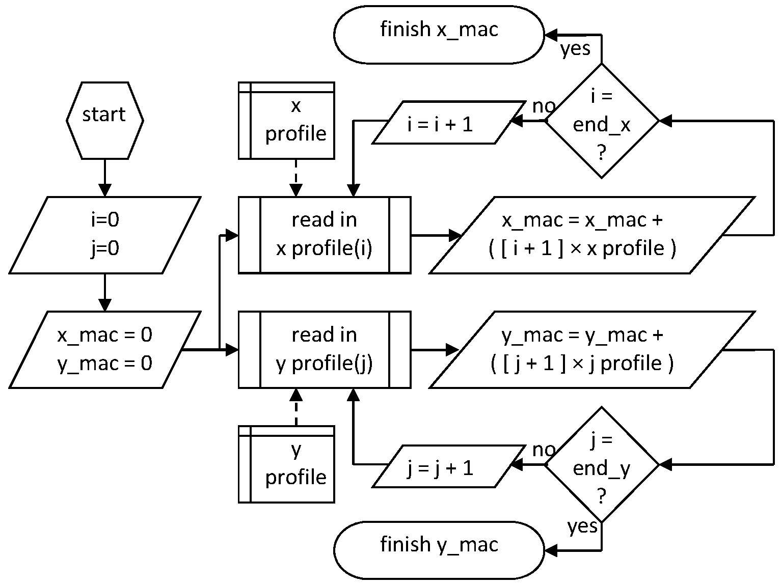
¾« & 8 t'sSastetirsg She x srs y muftipiy-«ccuRniia k>ns s« She Pmflbsr Ntoduts
The x any y multiply-accumulation values are calculated from the profiles once the Profiler Module has completely read in and processed an image. Data is read at 60 MHz from the profiles and passed into the multiply-accumulation sub-modules. The timing constraints of these sub-modules prevent them from being run at 120 MHz, which is why they must be processed afterwards in the 60 MHz clock domain of Figure 4.
Processing back to back frames using ike Profiler
Pixel data is written by the IBIS4-1300 at 20 MHz and processed by the Profiler Module at 30 MHz. The various processes for acquiring images, processing image data in the Profiler Module, the CPU reading the processed data from the Profiler Module and then transmitting these data down the Ethernet must be streamlined in order to process back to back frames. This is illustrated in Figure 9:

The Framestore is configured to continuously write images alternately into two buffers of SDRAM starting at page addresses 0x6000 and 0x9000 (the 32-bit summed image section of Figure 3). Even frame numbers are written to 0x6000 and the odd frame numbers are written to 0x9000.
While the IBIS4-1300 imager is writing a frame to the SDRAM, the CPU will read the status of the DMA Write Module to determine what buffer the frame is being written into. It will configure DMA Read Module 1 to read data from the buffer into which the current frame is being written. The CPU will then enable the trigger mode Profiler Module. When the trigger mode is enabled, the Profiler Module will reset all of the data registers processed from the previous frame and wipe the contents of the
Histogram block RAM. Under trigger mode, the Profiler Module will wait for the end of the current frame, at which point it will autonomously start processing the data written to the SDRAM and disable the trigger mode without any input from the CPU.
The CPU will transfer the processed data across the Ethernet to the Host PC. At the end of the data transfer, the Host PC transmits a byte to signal whether or not to acquire another frame. If another frame is requested, the CPU waits for the Profiler Module to finish processing before reading the processed data from the FPGA. The CPU enables the Profiler Module trigger mode before transmitting the next frame's processed data over the Ethernet.
The CPU features an l2C-bus interface. A piggyback circuit board can be interfaced on the 80-way AMP connector on the underside of the EVS in conjunction with the IBIS4-1300 imager headboard, which is mounted on the front of the EVS via the 50-way ERNI connector. This piggyback circuit board allows the CPU l2C-bus to set two Digital to Analogue Converters (DAC) to generate two output analogue voltages each. When the Host PC requests another frame, it can also upload new values to set the analogue output voltages to, based on the processed data acquired from the previous frame. The analogue voltages can then be used as a feedback signal to control the position of the beam under test.
Claims
1. A data processing system (100) comprising a first processor (1 16) having access to first configuration data; first configuration data (812) comprising at least a first configuration program for at least one of configuring and controlling a reconfigurable processor (102); the first processor being adapted to configure the reconfigurable processor using the first configuration data and the reconfigurable processor being arranged to operate according to the first configuration data (812).
2. A data processing system (100) as claimed in claim 1 , comprising second configuration data (814) comprising at least a second configuration program for configuring and controlling the reconfigurable processor (102); the first processor (116) being adapted to re-configure the reconfigurable processor (102) from a first configuration state corresponding to the first configuration data (812) to a second configuration state corresponding to the second configuration data (814).
3. A data processing system (100) as claimed any preceding claim, wherein at least one of the first configuration data (812) and the second configuration data (814) comprises at least one executable program for the first processor.
4. A data processing system (100) as claimed in any preceding claim, further comprising at least one of a second processor (1 12) and a third processor (1 14); at least one of the second (1 12) and third processor (1 14) being different to the first processor (116) and wherein at least one of the first and second configuration data comprises at least one of second processor configuration data (908) and third processor configuration data (918).
5. A data processing system (100) as claimed in any preceding claim, wherein any of the configuration data comprises at least one algorithm for execution by a respective one of the processors and the reconfigurable processor (1 12).
6. A data processing system (100) as claimed in any preceding claim, wherein the reconfigurable processor (102) is adapted to receive data from one or more than one sensor.
7. A data processing system (100) as claimed in any preceding claim, further comprising one or more than one memory (106) arranged to store data output from the reconfigurable processor (102).
22
8. A data processing system as claimed in claim (100), wherein the reconfigurable processor (102) is adapted to process the received data prior to outputting the processed data to the one or more than one memory.
9. A data processing system as claimed in either of claims 7 and 8, wherein the reconfigurable processor (102) is adapted to output data to selectable ones of the one or more than one memory (106) according to a predetermined pattern.
10. A data processing system (100) as claimed in claim 9, wherein the predetermined pattern is a round robin pattern
11. A data processing system (100) as claimed in any preceding claim, wherein the first configuration data (812) is arranged to configure the reconfigurable processor (102) to have a host controller (602); the host controller (602) being arranged to provide a memory interconnect such that at least the first processor (116) communicates or interacts with the reconfigurable processor (102) as if communicating with or interacting with a memory.
12. A data processing system (100) as claimed in any preceding claim, further comprising a memory mapped host bus (603) for hosting, in a memory mapped manner, at least one or more than one operable entity (604..620).
13. A data processing system (100) as claimed in claim 12, wherein the at least one or more than one operable entity (604..620) comprises a sensor control (606) for controlling communication with at least one sensor (607).
14. A data processing system (100) as claimed in claim 13, wherein the at least one or more than one operable entity (604..620) comprises a frame store (608) for storing data at least received from or associated with data the at least one sensor (607).
15. A data processing system (100) as claimed in claim any of claims 12 to 14, wherein the at least one or more than one operable entity (604..620) comprises a profiler (610) for performing an analysis of data such as at least one of calculating a profile, a histogram and a centre of gravity of the data.
16. A data processing system (100) as claimed in any of claims 12 to 15, wherein the at least one or more than one operable entity (604..620) comprises at least a signal processing module (612) adapted to perform signal processing operations on data presented to or accessible to the at least one signal processing module (612).
17. A data processing system (100) as claimed in any of claims 12 to 16, wherein the at least one or more than one operable entity (604..620) comprises a dynamic range processor (614) adapted to process data presented to or accessible to the dynamic range processor according to a respective dynamic range of said data.
23
18. A data processing system (100) as claimed in claim 17, wherein the respective dynamic range is at least one of prescribed or adaptable.
19. A data processing system (100) as claimed in any of claims 12 to 18, wherein the one or more than one operable entity (604..620) comprises one or more than one memory access channel (604) for outputting data to a memory (618) via a memory manager (616 and 620).
20. A data processing system (100) as claimed in claim 19, wherein the memory manager comprises at least one of a memory access multiplexor (616) and a memory controller (620).
21. A data processing system (100) as claimed in any preceding claim, further comprising an input-output interface (226A) adapted to cooperate with one or more than one external entity (228A, 230A).
22. A data processing system (100) as claimed in claim 21 , wherein the one or more than one external entity (228A, 230A) comprises at least one of a positioning system, a communication system, an inertial measurement unit, a magnetometer.
23. A data processing system (100) as claimed in any preceding claim, wherein the reconfigurable processor (102) is adapted to have at least one network controller (222A) for supporting communications over a network.
24. A data processing system (100) as claimed in any preceding claim, wherein the reconfigurable processor is arranged to have a further programming interface (216A) for receiving the first configuration data (812) or other configuration data (814).
25. A data processing system (100) as claimed in any preceding claim, further comprising at least one sensor interface via which at least first sensor data associated with at least a first sensor is received; the at least first sensor data being associated with the first configuration data.
26. A data processing system (100) as claimed in claim 25, comprising a plurality of configuration data; each associated with a respective sensor and being selectable by the first processor to configure the reconfigurable processor in response to connection of a sensor to a sensor interface.
27. A sensor interface for communicating with a sensor (607); the sensor comprising storage for storing identification data associated with the sensor (607); the identification data associated with the sensor having respective configuration data for adapting the configuration of a reconfigurable processor (102) according to the sensor or the
24 reconfigurable processor (102) of a system (100) as claimed in any preceding claim; the sensor interface being adapted to read the identification data.
28. A method of configuring a reconfigurable processor (102) within a heterogeneous processing environment; the method comprising the steps of
a. Detecting connection of a sensor (607) to the reconfigurable processor
(102);
b. Determining identification data (714) associated with the sensor (607); c. Retrieving configuration data (812) associated with the identification data (714) of the sensor (607); the configuration data comprising at least a first configuration program for at least one of configuring and controlling a reconfigurable processor (102);
d. Configuring the reconfigurable processor (102) according to the first configuration data (812).
29. A method as claimed in claim 28, further comprising operating the reconfigurable processor (102) configured according to the first configuration data (812) to obtain data from the sensor (607).
30. A method as claimed in claim 29, further comprising at least one of processing the obtained data and outputting the obtained data or outputting the processed obtained data to a selectable memory (106).
31. A method as claimed in any of claims 28 to 30 wherein said retrieving configuration data (812) associated with the identification data (714) of the sensor (607); the configuration data comprising at least a first program for data processing.
32. A sensor board for coupling to a sensor interface (606 and 701) of a reconfigurable processor (102); the sensor board comprising at least a sensor (604) adapted to output data via respective IO to the sensor interface; the sensor board further comprising storage (714) for storing identification data (712) associated with the sensor (607); the identification data (712) having associated configuration data adapted to configured the reconfigurable processor (102) for operation with the sensor (607).
33. A sensor board as claimed in claim 32, wherein the storage (714) comprises parameter data (718) associated with operating parameters of the sensor (607).
34. A heterogeneous processing environment comprising a plurality of heterogeneous processors and a data processing system as claimed in any of claims 1 to 27.
25
35. A data processing system substantially as described herein with reference to and/or as illustrated in the accompany drawings.
36. A method substantially as described herein with reference to and/or as illustrated in the accompany drawings.
37. A computer program substantially as described herein with reference to and/or as illustrated in the accompany drawings.
38. Machine readable storage substantially as described herein with reference to and/or as illustrated in the accompany drawings.
Applications Claiming Priority (2)
| Application Number | Priority Date | Filing Date | Title |
|---|---|---|---|
| GB1311682.7A GB2515573A (en) | 2013-06-28 | 2013-06-28 | Data processing system and method |
| GB1311682.7 | 2013-06-28 |
Publications (2)
| Publication Number | Publication Date |
|---|---|
| WO2014207438A2 true WO2014207438A2 (en) | 2014-12-31 |
| WO2014207438A3 WO2014207438A3 (en) | 2015-04-16 |
Family
ID=48999260
Family Applications (1)
| Application Number | Title | Priority Date | Filing Date |
|---|---|---|---|
| PCT/GB2014/051906 Ceased WO2014207438A2 (en) | 2013-06-28 | 2014-06-20 | Data processing system and method |
Country Status (2)
| Country | Link |
|---|---|
| GB (1) | GB2515573A (en) |
| WO (1) | WO2014207438A2 (en) |
Cited By (5)
| Publication number | Priority date | Publication date | Assignee | Title |
|---|---|---|---|---|
| DE102015103782A1 (en) * | 2015-03-16 | 2016-09-22 | Connaught Electronics Ltd. | Method for transmitting configuration information to a circuit unit, configuration device and motor vehicle |
| CN106453017A (en) * | 2016-11-11 | 2017-02-22 | 天津光电通信技术有限公司 | A kind of MII interface and GPMC interface data communication system and communication method |
| CN110418061A (en) * | 2019-08-26 | 2019-11-05 | Oppo广东移动通信有限公司 | Image processing method, image processor, photographing device and electronic equipment |
| RU2719427C1 (en) * | 2018-11-30 | 2020-04-17 | Федеральное государственное бюджетное образовательное учреждение высшего образования "Рязанский государственный радиотехнический университет" | Sensor matching device with electronic equipment |
| CN114762306A (en) * | 2019-11-26 | 2022-07-15 | 标致雪铁龙汽车股份有限公司 | Control method and control device for controlling communication device of vehicle |
Families Citing this family (1)
| Publication number | Priority date | Publication date | Assignee | Title |
|---|---|---|---|---|
| US10019260B2 (en) * | 2013-09-20 | 2018-07-10 | Via Alliance Semiconductor Co., Ltd | Fingerprint units comparing stored static fingerprints with dynamically generated fingerprints and reconfiguring processor settings upon a fingerprint match |
Family Cites Families (10)
| Publication number | Priority date | Publication date | Assignee | Title |
|---|---|---|---|---|
| US5784291A (en) * | 1994-12-22 | 1998-07-21 | Texas Instruments, Incorporated | CPU, memory controller, bus bridge integrated circuits, layout structures, system and methods |
| HU224946B1 (en) * | 1995-09-22 | 2006-04-28 | Owens Brockway Glass Container | System for checking containers by a field programmable gate array logic |
| US6216191B1 (en) * | 1997-10-15 | 2001-04-10 | Lucent Technologies Inc. | Field programmable gate array having a dedicated processor interface |
| US6417691B1 (en) * | 2000-08-29 | 2002-07-09 | Motorola, Inc. | Communication device with configurable module interface |
| US7013232B2 (en) * | 2001-08-15 | 2006-03-14 | National Insurance Corporation | Network-based system for configuring a measurement system using configuration information generated based on a user specification |
| US7320064B2 (en) * | 2004-07-23 | 2008-01-15 | Honeywell International Inc. | Reconfigurable computing architecture for space applications |
| US7343579B2 (en) * | 2004-11-30 | 2008-03-11 | Physical Sciences | Reconfigurable environmentally adaptive computing |
| US20110029254A1 (en) * | 2006-10-17 | 2011-02-03 | Endress + Hauser Gmbh + Co. Kg | Field device for determining and monitoring process variable in process automation systems |
| DE102009029495A1 (en) * | 2009-09-16 | 2011-03-24 | Endress + Hauser Conducta Gesellschaft für Mess- und Regeltechnik mbH + Co. KG | Transmitter for a multi-sensor system, in particular as field device for process automation technology and method for operating the transmitter |
| US20130107008A1 (en) * | 2011-10-31 | 2013-05-02 | Nokia Corporation | Method, apparatus and computer program product for capturing images |
-
2013
- 2013-06-28 GB GB1311682.7A patent/GB2515573A/en not_active Withdrawn
-
2014
- 2014-06-20 WO PCT/GB2014/051906 patent/WO2014207438A2/en not_active Ceased
Cited By (5)
| Publication number | Priority date | Publication date | Assignee | Title |
|---|---|---|---|---|
| DE102015103782A1 (en) * | 2015-03-16 | 2016-09-22 | Connaught Electronics Ltd. | Method for transmitting configuration information to a circuit unit, configuration device and motor vehicle |
| CN106453017A (en) * | 2016-11-11 | 2017-02-22 | 天津光电通信技术有限公司 | A kind of MII interface and GPMC interface data communication system and communication method |
| RU2719427C1 (en) * | 2018-11-30 | 2020-04-17 | Федеральное государственное бюджетное образовательное учреждение высшего образования "Рязанский государственный радиотехнический университет" | Sensor matching device with electronic equipment |
| CN110418061A (en) * | 2019-08-26 | 2019-11-05 | Oppo广东移动通信有限公司 | Image processing method, image processor, photographing device and electronic equipment |
| CN114762306A (en) * | 2019-11-26 | 2022-07-15 | 标致雪铁龙汽车股份有限公司 | Control method and control device for controlling communication device of vehicle |
Also Published As
| Publication number | Publication date |
|---|---|
| GB2515573A (en) | 2014-12-31 |
| GB201311682D0 (en) | 2013-08-14 |
| WO2014207438A3 (en) | 2015-04-16 |
Similar Documents
| Publication | Publication Date | Title |
|---|---|---|
| WO2014207438A2 (en) | Data processing system and method | |
| CN112235484B (en) | System and method for generating digital images | |
| CN102006484B (en) | Image processing device, image processing method, and program | |
| CN102037717B (en) | Image capture and image processing using monolithic camera arrays with heterogeneous imagers | |
| JP5786149B2 (en) | Universally packed pixel array camera system and method | |
| KR101664158B1 (en) | Intelligent computational imaging system | |
| US20160057332A1 (en) | Systems and Methods for High Dynamic Range Imaging Using Array Cameras | |
| EP4349003B1 (en) | Systems and methods for dark current compensation in single photon avalanche diode imagery | |
| US20090009654A1 (en) | Apparatus, method, and medium for generating image | |
| WO2009134316A1 (en) | Concentric exposure sequence for image sensor | |
| TWI823956B (en) | Exchanging an hdr-combined stream and associated exposures between a camera sensor module and a vision processing system | |
| CN105578067B (en) | Image generation method and device and terminal equipment | |
| CN113168673B (en) | Image processing method and device and electronic equipment | |
| CN114584752B (en) | Image color restoration methods and related equipment | |
| WO2019226211A1 (en) | Image signal processing for reducing lens flare | |
| US20140119595A1 (en) | Methods and apparatus for registering and warping image stacks | |
| WO2010104551A1 (en) | Cfa image with synthetic panchromatic image | |
| EP2420051A1 (en) | Producing full-color image with reduced motion blur | |
| CN107466473A (en) | More array camera imaging systems and its method | |
| CN105611185A (en) | Image generation method, device and terminal equipment | |
| US11699218B2 (en) | Method controlling image sensor parameters | |
| EP4349000A1 (en) | Systems and methods for power efficient image acquisition using single photon avalanche diodes (spads) | |
| JP2017069927A (en) | Image processing device, image processing method, and program | |
| CN107370917A (en) | Control method, electronic device, and computer-readable storage medium | |
| US20240037710A1 (en) | Image processing apparatus, imaging apparatus, image processing method, and program |
Legal Events
| Date | Code | Title | Description |
|---|---|---|---|
| 121 | Ep: the epo has been informed by wipo that ep was designated in this application |
Ref document number: 14732623 Country of ref document: EP Kind code of ref document: A2 |
|
| 122 | Ep: pct application non-entry in european phase |
Ref document number: 14732623 Country of ref document: EP Kind code of ref document: A2 |