WO2014205238A1 - Novel dielectric nano-structure for light trapping in solar cells - Google Patents
Novel dielectric nano-structure for light trapping in solar cells Download PDFInfo
- Publication number
- WO2014205238A1 WO2014205238A1 PCT/US2014/043214 US2014043214W WO2014205238A1 WO 2014205238 A1 WO2014205238 A1 WO 2014205238A1 US 2014043214 W US2014043214 W US 2014043214W WO 2014205238 A1 WO2014205238 A1 WO 2014205238A1
- Authority
- WO
- WIPO (PCT)
- Prior art keywords
- silicon nitride
- solar cell
- nitride layer
- nano
- semiconductor structure
- Prior art date
- Legal status (The legal status is an assumption and is not a legal conclusion. Google has not performed a legal analysis and makes no representation as to the accuracy of the status listed.)
- Ceased
Links
Classifications
-
- H—ELECTRICITY
- H10—SEMICONDUCTOR DEVICES; ELECTRIC SOLID-STATE DEVICES NOT OTHERWISE PROVIDED FOR
- H10F—INORGANIC SEMICONDUCTOR DEVICES SENSITIVE TO INFRARED RADIATION, LIGHT, ELECTROMAGNETIC RADIATION OF SHORTER WAVELENGTH OR CORPUSCULAR RADIATION
- H10F77/00—Constructional details of devices covered by this subclass
- H10F77/30—Coatings
- H10F77/306—Coatings for devices having potential barriers
- H10F77/311—Coatings for devices having potential barriers for photovoltaic cells
- H10F77/315—Coatings for devices having potential barriers for photovoltaic cells the coatings being antireflective or having enhancing optical properties
-
- H—ELECTRICITY
- H10—SEMICONDUCTOR DEVICES; ELECTRIC SOLID-STATE DEVICES NOT OTHERWISE PROVIDED FOR
- H10F—INORGANIC SEMICONDUCTOR DEVICES SENSITIVE TO INFRARED RADIATION, LIGHT, ELECTROMAGNETIC RADIATION OF SHORTER WAVELENGTH OR CORPUSCULAR RADIATION
- H10F77/00—Constructional details of devices covered by this subclass
- H10F77/70—Surface textures, e.g. pyramid structures
-
- Y—GENERAL TAGGING OF NEW TECHNOLOGICAL DEVELOPMENTS; GENERAL TAGGING OF CROSS-SECTIONAL TECHNOLOGIES SPANNING OVER SEVERAL SECTIONS OF THE IPC; TECHNICAL SUBJECTS COVERED BY FORMER USPC CROSS-REFERENCE ART COLLECTIONS [XRACs] AND DIGESTS
- Y02—TECHNOLOGIES OR APPLICATIONS FOR MITIGATION OR ADAPTATION AGAINST CLIMATE CHANGE
- Y02E—REDUCTION OF GREENHOUSE GAS [GHG] EMISSIONS, RELATED TO ENERGY GENERATION, TRANSMISSION OR DISTRIBUTION
- Y02E10/00—Energy generation through renewable energy sources
- Y02E10/50—Photovoltaic [PV] energy
Definitions
- This invention relates to solar cells.
- Nano-structuring of solar cells has been considered for improving various aspects of solar cell performance, such as reducing reflection loss.
- US 2009/0261353 is an example where silicon nanostructures are coated with silicon oxide or silicon nitride.
- WO 2013/171286 is an example where a solar cell includes cone-shaped
- This work relates to a dielectric (e.g., S1 3 N 4 ) anti- reflection (AR) coating that is nano-structured (e.g., nano-pyramids ) .
- a dielectric e.g., S1 3 N 4
- AR anti- reflection
- nano-structured e.g., nano-pyramids
- the light absorption in the solar cell can be significantly enhanced, and the absorbing layer thickness needed in the solar cell can be significantly reduced.
- a planar interface between the window layer and the solar cell advantageously avoids nano-structuring in the active parts of the solar cell, thereby improving electrical performance.
- the reflection loss at this interface can end up having a negligible effect on device performance.
- the nano-structured dielectric window layer of the present work provides light trapping over a greater spectral range and also desirably reduces the effect of angle of incidence on solar cell reflection/absorption.
- FIG . 1 shows an exemplary embodiment of the inve
- FIG. 2 shows an exemplary solar cell layer structure suitable for use in embodiments of the invention.
- FIG. 3 is a scanning electron microscope (SEM) image of a fabricated device.
- FIGs . 4A-G show an exemplary fabrication sequence.
- FIG. 5 shows simulated absorption in a 200 nm thick GaAs layer with and without a nano-structured silicon nitride window layer.
- FIG. 6 shows measured normal incidence reflection from a solar cell with and without a nano-structured silicon nitride window layer.
- FIG. 7 shows measured reflection vs. incident angle from a solar cell with and without a nano-structured silicon nitride window layer.
- FIG. 8 shows measured current-voltage curves from various solar cells.
- FIG. 9 shows measured external quantum efficiency from the solar cells of FIG. 8.
- FIG. 1 shows an exemplary embodiment of the invention.
- semiconductor structure 102 includes an active region where charge carriers can be generated by absorption of light.
- a silicon nitride layer 106 is disposed on the semiconductor structure 102.
- the interface between semiconductor structure 102 and silicon nitride layer 106 is substantially planar.
- the silicon nitride layer 106 has nano-scale features at a surface of the silicon nitride layer facing away from the semiconductor structure, as shown.
- nano-scale features are defined as having height and lateral dimensions of 2 microns or less, and preferably between about 0.5 microns to about 1.5 microns.
- an optional top contact 104 is shown.
- silicon nitride is particularly suitable as a material for the window layer because 1) it is a material that is compatible with a wide variety of semiconductor processing, 2) it is sufficiently transparent for wavelengths in the solar spectrum, and 3) it has a desirable trade-off of index vs. absorption. As shown in Table 1 below, reflection tends to decrease as the index of the window layer increases for indices near 2.0. However, the band gap of silicon nitride (index 2.0) is about 5.3 eV, while higher index materials (e.g., T1O 2 index 2.3, ZnS index 2.4) have much lower band gaps (e.g., T1O 2 band gap 3.6 eV, ZnS band gap 3.2 eV) . Thus increasing the index to values higher than 2.0 with technologically reasonable materials will undesirably increase optical loss in the window layer due to absorption.
- Table 1 Reflection vs. window layer index (simulations of spectrum averaged reflection based on AM 1.5G standard solar spectrum) .
- the nano-scale features are pyramids, truncated pyramids, cones and/or truncated cones.
- Pyramids have facets on their lateral surfaces, while cones have smoothly curved lateral surfaces. Both pyramids and cones can have the top come to a point or can be truncated structures with a flat top surface.
- features preferably have an aspect ratio in a range from about 1 to about 2.
- aspect ratio is defined as the ratio of feature height to feature width at the widest point (which is typically at the base of the feature) .
- the total thickness of silicon nitride layer 106 is preferably in a range from about 0.5 microns to about 1.5 microns. Here total thickness is defined as the distance between the 102-106 interface and the tops of the nano- scale features. In some cases, it is preferred for layer 106 to have a two part structure, where a first part 108 of layer 106 includes the nano-scale features and a second part 110 of layer 106 is uniform. Second part 110 is sandwiched between first part 108 and semiconductor
- first part 108 is
- FIG . 2 shows an exemplary solar cell layer structure suitable for use in embodiments of the invention as semiconductor structure 102 in FIG . 1 .
- 202 is a p-type silicon substrate (doping 1 ⁇ 10 15 cm -3 )
- 204 is a p-type silicon layer (thickness 1.7 ⁇ , doping 3 ⁇ 10 18 cm -3 )
- 206 is an intrinsic silicon layer (thickness 0.9 ⁇ )
- 208 is an n-type silicon layer (thickness 0.3 ⁇ , doping 1 x 10 19 cm “3 ) .
- the active region of semiconductor structure 102 can include silicon and/or compound semiconductors.
- the active region thickness is preferably in a range from about 100 nm to about 3 microns. In cases where the active region is silicon, the active region thickness is
- FIG. 3 is a scanning electron microscope (SEM) image of a fabricated device. Here it is apparent that nano- scale structures in silicon nitride have successfully been fabricated .
- FIGs . 4A-G show an exemplary fabrication sequence.
- a method of making solar cells according to this work includes:
- Forming the nano-scale features can include:
- layer 106 can act as a passivation layer for semiconductor structure 102 to reduce surface/interface recombination of charge carriers .
- FIG. 4A shows silicon nitride 106 disposed on
- FIG. 4B shows the result of depositing masking particles 402 on silicon nitride 106.
- these masking particles can be silicon oxide nano-spheres .
- FIG. 4C shows the result of etching with an etch that preferentially etches silicon nitride 106 relative to the masking particles 402.
- this etch can be a CF 4 plasma etch.
- FIG. 4D shows the result of removing the masking particles 402. If this step is performed with an etch, any etch that preferentially etches masking particles 402 relative to silicon nitride can be employed.
- FIG. 4E shows the result of deposition and patterning of photoresist 404.
- FIG. 4F shows the result of etching silicon nitride in areas left exposed by the patterning of FIG. 4E. Any etch that preferentially etches silicon nitride relative to silicon and relative to photoresist 404 can be employed for this step.
- buffered oxide etch (BOE) can be employed.
- FIG. 4G shows a final structure obtained by removal of photoresist 404 and deposition of metal contact 104.
- FIG. 5 shows simulated absorption in a 200 nm thick
- FIG. 6 shows measured normal incidence reflection from a solar cell with and without a nano-structured silicon nitride window layer.
- the nano-structured window layer leads to less than 5% reflection in the visible part and near-infrared part of the spectrum.
- FIG. 7 shows measured reflection vs. incident angle from a solar cell with and without a nano-structured silicon nitride window layer.
- FIG. 8 shows measured current-voltage curves from various solar cells.
- SL ARC is an abbreviation of single-layer anti-reflection coating.
- V oc open-circuit voltage
- J sc short-circuit current
- FF fill factor
- Eff. efficiency
- Table 2 Solar cell performance for various window layer configurations .
- FIG . 9 shows measured external quantum efficiency
- EQE from the solar cells of FIG . 8 .
- the EQE is enhanced by over 30% by the nano- structured window layer.
- the EQE enhancement decreases to about 15%, which is attributed to reduced carrier collection efficiency in this part of the spectrum in the experimental devices.
- the single-layer anti-reflection coating is seen to have an undesirable wavelength-dependence in its effect on efficiency.
Landscapes
- Photovoltaic Devices (AREA)
Abstract
This work relates to a dielectric (e.g., S13N4) anti- reflection (AR) coating that is nano-structured (e.g., nano-pyramids ). By including such nano-structures as part of a window layer in a solar cell, the light absorption in the solar cell can be significantly enhanced, and the absorbing layer thickness needed in the solar cell can be significantly reduced. Furthermore, a planar interface between the window layer and the solar cell advantageously avoids nano-structuring in the active parts of the solar cell, thereby improving electrical performance.
Description
Novel Dielectric Structure for Light Trapping in
Solar Cells by
Yangsen Kang, Dong Liang, Yusi Chen, Yijie Huo, and
James S. Harris, Jr.
FIELD OF THE INVENTION
This invention relates to solar cells.
BACKGROUND
Nano-structuring of solar cells has been considered for improving various aspects of solar cell performance, such as reducing reflection loss. US 2009/0261353 is an example where silicon nanostructures are coated with silicon oxide or silicon nitride. WO 2013/171286 is an example where a solar cell includes cone-shaped
nanostructures .
However, conventional nano-structured solar cells tend to experience a trade off where improved optical
performance (e.g., reduced reflection) is obtained, but electrical performance is undesirably degraded (e.g., nanostructured solar cell active regions can have excess surface recombination) . Accordingly, it would be an advance in the art to avoid making a performance compromise along these lines.
SUMMARY
This work relates to a dielectric (e.g., S13N4) anti- reflection (AR) coating that is nano-structured (e.g., nano-pyramids ) . By including such nano-structures as part of a window layer in a solar cell, the light absorption in the solar cell can be significantly enhanced, and the absorbing layer thickness needed in the solar cell can be significantly reduced. Furthermore, a planar interface between the window layer and the solar cell advantageously avoids nano-structuring in the active parts of the solar cell, thereby improving electrical performance.
Surprisingly, the reflection loss at this interface can end up having a negligible effect on device performance.
High open circuit voltage and high fill factor as well as high short circuit current can be obtained in such nanostructured solar cells. Therefore, the efficiency of solar cells can be significantly improved. In addition, reduction of absorbing material thickness can reduce the solar cell cost. This approach is broadly applicable, e.g., to anti- reflection and light trapping for most kinds of solar cells, such as silicon, III-V, CIGS (copper indium gallium selenide) , CdTe solar cells etc.
Compared with traditional anti-reflective coatings, the nano-structured dielectric window layer of the present work provides light trapping over a greater spectral range and also desirably reduces the effect of angle of incidence on solar cell reflection/absorption.
BRIEF DESCRIPTION OF THE DRAWINGS
FIG . 1 shows an exemplary embodiment of the inve
FIG. 2 shows an exemplary solar cell layer structure suitable for use in embodiments of the invention.
FIG. 3 is a scanning electron microscope (SEM) image of a fabricated device.
FIGs . 4A-G show an exemplary fabrication sequence.
FIG. 5 shows simulated absorption in a 200 nm thick GaAs layer with and without a nano-structured silicon nitride window layer.
FIG. 6 shows measured normal incidence reflection from a solar cell with and without a nano-structured silicon nitride window layer.
FIG. 7 shows measured reflection vs. incident angle from a solar cell with and without a nano-structured silicon nitride window layer. FIG. 8 shows measured current-voltage curves from various solar cells.
FIG. 9 shows measured external quantum efficiency from the solar cells of FIG. 8.
DETAILED DESCRIPTION
FIG. 1 shows an exemplary embodiment of the invention. In this solar cell, semiconductor structure 102 includes an active region where charge carriers can be generated by absorption of light. A silicon nitride layer 106 is disposed on the semiconductor structure 102. The interface between semiconductor structure 102 and silicon nitride layer 106 is substantially planar. The silicon nitride layer 106 has nano-scale features at a surface of the silicon nitride layer facing away from the semiconductor structure, as shown. Here nano-scale features are defined
as having height and lateral dimensions of 2 microns or less, and preferably between about 0.5 microns to about 1.5 microns. On FIG . 1 , an optional top contact 104 is shown.
We have found that silicon nitride is particularly suitable as a material for the window layer because 1) it is a material that is compatible with a wide variety of semiconductor processing, 2) it is sufficiently transparent for wavelengths in the solar spectrum, and 3) it has a desirable trade-off of index vs. absorption. As shown in Table 1 below, reflection tends to decrease as the index of the window layer increases for indices near 2.0. However, the band gap of silicon nitride (index 2.0) is about 5.3 eV, while higher index materials (e.g., T1O2 index 2.3, ZnS index 2.4) have much lower band gaps (e.g., T1O2 band gap 3.6 eV, ZnS band gap 3.2 eV) . Thus increasing the index to values higher than 2.0 with technologically reasonable materials will undesirably increase optical loss in the window layer due to absorption.

Table 1: Reflection vs. window layer index (simulations of spectrum averaged reflection based on AM 1.5G standard solar spectrum) .
Preferably the nano-scale features are pyramids, truncated pyramids, cones and/or truncated cones. Pyramids have facets on their lateral surfaces, while cones have smoothly curved lateral surfaces. Both pyramids and cones
can have the top come to a point or can be truncated structures with a flat top surface. The nano-scale
features preferably have an aspect ratio in a range from about 1 to about 2. Here the aspect ratio is defined as the ratio of feature height to feature width at the widest point (which is typically at the base of the feature) .
Practice of the invention does not depend critically on the lateral arrangement of the nano-scale features. For example, suitable arrangements for these features include, but are not limited to: square lattices and hexagonal lattices .
The total thickness of silicon nitride layer 106 is preferably in a range from about 0.5 microns to about 1.5 microns. Here total thickness is defined as the distance between the 102-106 interface and the tops of the nano- scale features. In some cases, it is preferred for layer 106 to have a two part structure, where a first part 108 of layer 106 includes the nano-scale features and a second part 110 of layer 106 is uniform. Second part 110 is sandwiched between first part 108 and semiconductor
structure 102. The thickness of first part 108 is
preferably in a range from about 0.5 microns to about 1.5 microns. The thickness of second part 110 is preferably in a range from about 50 nm to about 200 nm. Practice of the invention does not depend critically on details of semiconductor structure 102. Any kind of solar cell can benefit from a nano-structured dielectric window layer as described here, including but not limited to: silicon solar cells, compound semiconductor solar cells, single junction solar cells, and multi-j unction solar cells. FIG . 2 shows an exemplary solar cell layer structure suitable for use in embodiments of the invention as semiconductor structure 102 in FIG . 1 . In this example,
202 is a p-type silicon substrate (doping 1 χ 1015 cm-3) , 204 is a p-type silicon layer (thickness 1.7 μιτι, doping 3 χ 1018 cm-3), 206 is an intrinsic silicon layer (thickness 0.9 μιη) , and 208 is an n-type silicon layer (thickness 0.3 μιτι, doping 1 x 1019 cm"3) .
The active region of semiconductor structure 102 can include silicon and/or compound semiconductors. In cases where the active region includes a compound semiconductor, the active region thickness is preferably in a range from about 100 nm to about 3 microns. In cases where the active region is silicon, the active region thickness is
preferably in a range from about 1 micron to about 100 microns .
FIG. 3 is a scanning electron microscope (SEM) image of a fabricated device. Here it is apparent that nano- scale structures in silicon nitride have successfully been fabricated .
FIGs . 4A-G show an exemplary fabrication sequence.
This sequence is provided as an illustrative example, and any other approach for providing nano-structured window layers as described above can also be employed. In general terms, a method of making solar cells according to this work includes:
1) providing a semiconductor structure including an active region where charge carriers can be generated by absorption of light;
2) depositing a silicon nitride layer on the
semiconductor structure, where an interface between the semiconductor structure and the silicon nitride layer is substantially planar; and
3) forming nano-scale features at a surface of the silicon nitride layer facing away from the semiconductor structure .
Forming the nano-scale features can include:
4) depositing masking particles on the silicon nitride layer; and
5) etching the silicon nitride layer with an etch that preferentially etches silicon nitride relative to the masking particles to form the nano-scale features. This kind of fabrication sequence can advantageously be used to provide a nearly ideal interface between
semiconductor structure 102 and silicon nitride layer 106 in terms of electrical properties. In other words, layer 106 can act as a passivation layer for semiconductor structure 102 to reduce surface/interface recombination of charge carriers .
FIG. 4A shows silicon nitride 106 disposed on
semiconductor structure 102. FIG. 4B shows the result of depositing masking particles 402 on silicon nitride 106. For example, these masking particles can be silicon oxide nano-spheres . FIG. 4C shows the result of etching with an etch that preferentially etches silicon nitride 106 relative to the masking particles 402. For example, this etch can be a CF4 plasma etch. FIG. 4D shows the result of removing the masking particles 402. If this step is performed with an etch, any etch that preferentially etches masking particles 402 relative to silicon nitride can be employed. FIG. 4E shows the result of deposition and patterning of photoresist 404. FIG. 4F shows the result of etching silicon nitride in areas left exposed by the patterning of FIG. 4E. Any etch that preferentially etches silicon nitride relative to silicon and relative to
photoresist 404 can be employed for this step. For
example, buffered oxide etch (BOE) can be employed.
FIG. 4G shows a final structure obtained by removal of photoresist 404 and deposition of metal contact 104. FIG. 5 shows simulated absorption in a 200 nm thick
GaAs layer with and without a nano-structured silicon nitride window layer. These results show strong light trapping due to the nano-structured window layer (i.e., an 88% absorption enhancement relative to the control
structure.) This is attributed to coupling of incident light to a propagating mode in the 200 nm GaAs layer by scattering from the nano-structures of the silicon nitride window layer. Such enhanced absorption enables the use of thinner solar cell active regions. FIG. 6 shows measured normal incidence reflection from a solar cell with and without a nano-structured silicon nitride window layer. Here we see that the nano-structured window layer leads to less than 5% reflection in the visible part and near-infrared part of the spectrum. FIG. 7 shows measured reflection vs. incident angle from a solar cell with and without a nano-structured silicon nitride window layer. Here reflection is
spectrally averaged using the AM 1.5G standard solar spectrum. Broad-band anti-reflection is seen even for large angles of incidence. The reflection is less than 10% for incidence angles of 60 degrees of less.
FIG. 8 shows measured current-voltage curves from various solar cells. Here "SL ARC" is an abbreviation of single-layer anti-reflection coating. Results from these curves for open-circuit voltage (Voc) , short-circuit current ( Jsc) , fill factor (FF) and efficiency (Eff.) are given in Table 2 below. Here we see that the nano-structured window
layer enhances Jsc by 32% and enhances the efficiency by 43% relative to a structure having no window layer.
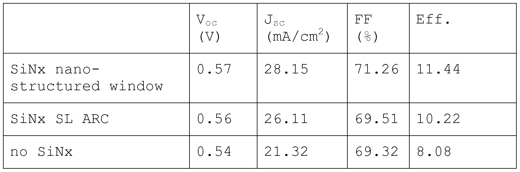
Table 2: Solar cell performance for various window layer configurations .
FIG . 9 shows measured external quantum efficiency
(EQE) from the solar cells of FIG . 8 . In the visible light region, the EQE is enhanced by over 30% by the nano- structured window layer. In the near-infrared region, the EQE enhancement decreases to about 15%, which is attributed to reduced carrier collection efficiency in this part of the spectrum in the experimental devices. The single-layer anti-reflection coating is seen to have an undesirable wavelength-dependence in its effect on efficiency.
Claims
1. A solar cell comprising: a semiconductor structure including an active region where charge carriers can be generated by absorption of light ;
a silicon nitride layer disposed on the semiconductor structure ;
wherein an interface between the semiconductor structure and the silicon nitride layer is substantially planar; and wherein the silicon nitride layer has nano-scale features at a surface of the silicon nitride layer facing away from the semiconductor structure.
2. The solar cell of claim 1, wherein the nano-scale features comprise features selected from the group
consisting of: pyramids, truncated pyramids, cones and truncated cones.
3. The solar cell of claim 1, wherein the nano-scale features have an aspect ratio defined as a ratio of feature height to feature width, and wherein the aspect ratio is in a range from about 1 to about 2.
4. The solar cell of claim 1, wherein the active region comprises one or more materials selected from the group consisting of: silicon and compound semiconductors.
5. The solar cell of claim 1, wherein the active region comprises a compound semiconductor and wherein a thickness of the active region is in a range from about 100 nm to about 3 microns.
6. The solar cell of claim 1, wherein the active region comprises silicon and wherein a thickness of the active region is in a range from about 1 micron to about 100 microns .
7. The solar cell of claim 1, wherein a thickness of the silicon nitride layer is in a range from about 0.5 microns to about 1.5 microns.
8. The solar cell of claim 1, wherein a first part of the silicon nitride layer includes the nano-scale features and a second part of the silicon nitride layer is uniform and is sandwiched between the semiconductor structure and the first part of the silicon nitride layer.
9. The solar cell of claim 7, wherein a thickness of the first part of the silicon nitride layer is in a range from about 0.5 microns to about 1.5 microns.
10. The solar cell of claim 7, wherein a thickness of the second part of the silicon nitride layer is in a range from about 50 nm to about 200 nm.
11. A method of making a solar cell, the method comprising:
providing a semiconductor structure including an active region where charge carriers can be generated by absorption of light; depositing a silicon nitride layer on the
semiconductor structure, wherein an interface between the semiconductor structure and the silicon nitride layer is substantially planar; and forming nano-scale features at a surface of the silicon nitride layer facing away from the semiconductor structure .
12. The method of claim 11, wherein the forming nano-scale features comprises:
depositing masking particles on the silicon nitride layer; and etching the silicon nitride layer with an etch that preferentially etches silicon nitride relative to the masking particles to form the nano-scale features.
Applications Claiming Priority (2)
| Application Number | Priority Date | Filing Date | Title |
|---|---|---|---|
| US201361836866P | 2013-06-19 | 2013-06-19 | |
| US61/836,866 | 2013-06-19 |
Publications (1)
| Publication Number | Publication Date |
|---|---|
| WO2014205238A1 true WO2014205238A1 (en) | 2014-12-24 |
Family
ID=51179175
Family Applications (1)
| Application Number | Title | Priority Date | Filing Date |
|---|---|---|---|
| PCT/US2014/043214 Ceased WO2014205238A1 (en) | 2013-06-19 | 2014-06-19 | Novel dielectric nano-structure for light trapping in solar cells |
Country Status (1)
| Country | Link |
|---|---|
| WO (1) | WO2014205238A1 (en) |
Cited By (3)
| Publication number | Priority date | Publication date | Assignee | Title |
|---|---|---|---|---|
| WO2018044240A1 (en) * | 2016-09-05 | 2018-03-08 | Agency For Science, Technology And Research | A method of forming nano-patterns on a substrate |
| CN109581559A (en) * | 2019-01-29 | 2019-04-05 | 香港中文大学(深圳) | A kind of double grating nanostructure and preparation method thereof of quadrangle bipyramid array composition |
| WO2025027236A1 (en) * | 2023-08-01 | 2025-02-06 | Teknologian Tutkimuskeskus Vtt Oy | An antireflection coating and method for manufacturing such |
Citations (4)
| Publication number | Priority date | Publication date | Assignee | Title |
|---|---|---|---|---|
| US20090261353A1 (en) | 2005-10-10 | 2009-10-22 | X-Fab Semiconductor Foundries Ag | Production of self-organized pin-type nanostructures, and the rather extensive applications thereof |
| US20110146779A1 (en) * | 2009-12-22 | 2011-06-23 | National Chiao Tung University | Sub-wavelength structure layer, method for fabricating the same and photoelectric conversion device applying the same |
| WO2012036760A1 (en) * | 2010-09-16 | 2012-03-22 | Specmat, Inc. | Method, process and fabrication technology for high-efficency low-cost crytalline silicon solar cells |
| WO2013171286A1 (en) | 2012-05-15 | 2013-11-21 | Danmarks Tekniske Universitet | Solar cells having a nanostructured antireflection layer |
-
2014
- 2014-06-19 WO PCT/US2014/043214 patent/WO2014205238A1/en not_active Ceased
Patent Citations (4)
| Publication number | Priority date | Publication date | Assignee | Title |
|---|---|---|---|---|
| US20090261353A1 (en) | 2005-10-10 | 2009-10-22 | X-Fab Semiconductor Foundries Ag | Production of self-organized pin-type nanostructures, and the rather extensive applications thereof |
| US20110146779A1 (en) * | 2009-12-22 | 2011-06-23 | National Chiao Tung University | Sub-wavelength structure layer, method for fabricating the same and photoelectric conversion device applying the same |
| WO2012036760A1 (en) * | 2010-09-16 | 2012-03-22 | Specmat, Inc. | Method, process and fabrication technology for high-efficency low-cost crytalline silicon solar cells |
| WO2013171286A1 (en) | 2012-05-15 | 2013-11-21 | Danmarks Tekniske Universitet | Solar cells having a nanostructured antireflection layer |
Non-Patent Citations (3)
| Title |
|---|
| CHANDRA SAHOO K ET AL: "Shape Effect of Silicon Nitride Subwavelength Structure on Reflectance for Silicon Solar Cells", IEEE TRANSACTIONS ON ELECTRON DEVICES, IEEE SERVICE CENTER, PISACATAWAY, NJ, US, vol. 57, no. 10, 1 October 2010 (2010-10-01), pages 2427 - 2433, XP011316021, ISSN: 0018-9383 * |
| KARTIKA SAHOO ET AL: "Fabrication of Antireflective Sub-Wavelength Structures on Silicon Nitride Using Nano Cluster Mask for Solar Cell Application", NANOSCALE RESEARCH LETTERS, vol. 4, no. 7, 22 April 2009 (2009-04-22), pages 680 - 683, XP055141904, ISSN: 1931-7573, DOI: 10.1007/s11671-009-9297-7 * |
| SAHOO KARTIKA CHANDRA, LIN MEN-KU, CHANG EDWARD-YI, TINH TRAN BINH, LI YIMING, HUANG JIN-HUA: "Silicon Nitride Nanopillars and Nanocones Formed by Nickel Nanoclusters and Inductively Coupled Plasma Etching for Solar Cell Application", JAPANESE JOURNAL OF APPLIED PHYSICS, vol. 48, no. 12, 21 December 2009 (2009-12-21), pages 126508-1 - 126508-4, XP002730145, ISSN: 0021-4922, DOI: 10.1143/JJAP.48.126508 * |
Cited By (5)
| Publication number | Priority date | Publication date | Assignee | Title |
|---|---|---|---|---|
| WO2018044240A1 (en) * | 2016-09-05 | 2018-03-08 | Agency For Science, Technology And Research | A method of forming nano-patterns on a substrate |
| US11287551B2 (en) | 2016-09-05 | 2022-03-29 | Agency For Science, Technology And Research | Method of forming nano-patterns on a substrate |
| CN109581559A (en) * | 2019-01-29 | 2019-04-05 | 香港中文大学(深圳) | A kind of double grating nanostructure and preparation method thereof of quadrangle bipyramid array composition |
| CN109581559B (en) * | 2019-01-29 | 2021-02-02 | 香港中文大学(深圳) | Double grating nanostructure composed of quadrangular bipyramid array and preparation method thereof |
| WO2025027236A1 (en) * | 2023-08-01 | 2025-02-06 | Teknologian Tutkimuskeskus Vtt Oy | An antireflection coating and method for manufacturing such |
Similar Documents
| Publication | Publication Date | Title |
|---|---|---|
| CN103999242B (en) | Crystalline silicon solar cell, solar cell module and manufacturing method thereof | |
| EP2149915A2 (en) | Method of manufacturing photovoltaic device | |
| WO2012020682A1 (en) | Crystalline silicon solar cell | |
| MX2012001218A (en) | SOLAR CELL AND MANUFACTURING METHOD OF THE SAME. | |
| WO2013161127A1 (en) | Solar cell, solar cell manufacturing method, and solar cell module | |
| US20120000506A1 (en) | Photovoltaic module and method of manufacturing the same | |
| JP5813204B2 (en) | Manufacturing method of solar cell | |
| US20110146779A1 (en) | Sub-wavelength structure layer, method for fabricating the same and photoelectric conversion device applying the same | |
| CN107710419A (en) | Solar cell and solar module | |
| US9761749B2 (en) | Photoelectric conversion device | |
| JP5948148B2 (en) | Photoelectric conversion device | |
| WO2013094233A1 (en) | Solar cell, method for producing same, and solar cell module | |
| TWI474488B (en) | Solar battery | |
| Ho et al. | An efficient light-harvesting scheme using SiO2 nanorods for InGaN multiple quantum well solar cells | |
| JP6114603B2 (en) | Crystalline silicon solar cell, method for manufacturing the same, and solar cell module | |
| JP5541980B2 (en) | Crystalline silicon solar cell and manufacturing method thereof | |
| WO2014205238A1 (en) | Novel dielectric nano-structure for light trapping in solar cells | |
| US20140090705A1 (en) | Photoelectric conversion element | |
| KR101190197B1 (en) | Solar cells using substrate integrated with antireflection nano structure and method for fabricating the same | |
| CN104662673B (en) | The manufacture method of photo-electric conversion element and photo-electric conversion element | |
| KR20150090606A (en) | Solar cell and manufacturing method thereof | |
| KR20120060185A (en) | Solar cells using substrate integrated with antireflection nano structure and method for fabricating the same | |
| WO2012160764A1 (en) | Photoelectric conversion element | |
| US20110308585A1 (en) | Dual transparent conductive material layer for improved performance of photovoltaic devices | |
| US20110308584A1 (en) | Surface treatment of transparent conductive material films for improvement of photovoltaic devices |
Legal Events
| Date | Code | Title | Description |
|---|---|---|---|
| 121 | Ep: the epo has been informed by wipo that ep was designated in this application |
Ref document number: 14739317 Country of ref document: EP Kind code of ref document: A1 |
|
| NENP | Non-entry into the national phase |
Ref country code: DE |
|
| 122 | Ep: pct application non-entry in european phase |
Ref document number: 14739317 Country of ref document: EP Kind code of ref document: A1 |