WO2014199889A1 - マイクロ流体デバイス及び誘電泳動装置 - Google Patents
マイクロ流体デバイス及び誘電泳動装置 Download PDFInfo
- Publication number
- WO2014199889A1 WO2014199889A1 PCT/JP2014/064919 JP2014064919W WO2014199889A1 WO 2014199889 A1 WO2014199889 A1 WO 2014199889A1 JP 2014064919 W JP2014064919 W JP 2014064919W WO 2014199889 A1 WO2014199889 A1 WO 2014199889A1
- Authority
- WO
- WIPO (PCT)
- Prior art keywords
- electrode
- microfluidic device
- insulating sheet
- flow path
- transparent film
- Prior art date
- Legal status (The legal status is an assumption and is not a legal conclusion. Google has not performed a legal analysis and makes no representation as to the accuracy of the status listed.)
- Ceased
Links
Images






Classifications
-
- G—PHYSICS
- G01—MEASURING; TESTING
- G01N—INVESTIGATING OR ANALYSING MATERIALS BY DETERMINING THEIR CHEMICAL OR PHYSICAL PROPERTIES
- G01N27/00—Investigating or analysing materials by the use of electric, electrochemical, or magnetic means
- G01N27/26—Investigating or analysing materials by the use of electric, electrochemical, or magnetic means by investigating electrochemical variables; by using electrolysis or electrophoresis
- G01N27/416—Systems
- G01N27/447—Systems using electrophoresis
-
- B—PERFORMING OPERATIONS; TRANSPORTING
- B01—PHYSICAL OR CHEMICAL PROCESSES OR APPARATUS IN GENERAL
- B01L—CHEMICAL OR PHYSICAL LABORATORY APPARATUS FOR GENERAL USE
- B01L3/00—Containers or dishes for laboratory use, e.g. laboratory glassware; Droppers
- B01L3/50—Containers for the purpose of retaining a material to be analysed, e.g. test tubes
- B01L3/502—Containers for the purpose of retaining a material to be analysed, e.g. test tubes with fluid transport, e.g. in multi-compartment structures
- B01L3/5027—Containers for the purpose of retaining a material to be analysed, e.g. test tubes with fluid transport, e.g. in multi-compartment structures by integrated microfluidic structures, i.e. dimensions of channels and chambers are such that surface tension forces are important, e.g. lab-on-a-chip
- B01L3/502707—Containers for the purpose of retaining a material to be analysed, e.g. test tubes with fluid transport, e.g. in multi-compartment structures by integrated microfluidic structures, i.e. dimensions of channels and chambers are such that surface tension forces are important, e.g. lab-on-a-chip characterised by the manufacture of the container or its components
-
- B—PERFORMING OPERATIONS; TRANSPORTING
- B03—SEPARATION OF SOLID MATERIALS USING LIQUIDS OR USING PNEUMATIC TABLES OR JIGS; MAGNETIC OR ELECTROSTATIC SEPARATION OF SOLID MATERIALS FROM SOLID MATERIALS OR FLUIDS; SEPARATION BY HIGH-VOLTAGE ELECTRIC FIELDS
- B03C—MAGNETIC OR ELECTROSTATIC SEPARATION OF SOLID MATERIALS FROM SOLID MATERIALS OR FLUIDS; SEPARATION BY HIGH-VOLTAGE ELECTRIC FIELDS
- B03C5/00—Separating dispersed particles from liquids by electrostatic effect
- B03C5/005—Dielectrophoresis, i.e. dielectric particles migrating towards the region of highest field strength
-
- B—PERFORMING OPERATIONS; TRANSPORTING
- B03—SEPARATION OF SOLID MATERIALS USING LIQUIDS OR USING PNEUMATIC TABLES OR JIGS; MAGNETIC OR ELECTROSTATIC SEPARATION OF SOLID MATERIALS FROM SOLID MATERIALS OR FLUIDS; SEPARATION BY HIGH-VOLTAGE ELECTRIC FIELDS
- B03C—MAGNETIC OR ELECTROSTATIC SEPARATION OF SOLID MATERIALS FROM SOLID MATERIALS OR FLUIDS; SEPARATION BY HIGH-VOLTAGE ELECTRIC FIELDS
- B03C5/00—Separating dispersed particles from liquids by electrostatic effect
- B03C5/02—Separators
- B03C5/022—Non-uniform field separators
- B03C5/026—Non-uniform field separators using open-gradient differential dielectric separation, i.e. using electrodes of special shapes for non-uniform field creation, e.g. Fluid Integrated Circuit [FIC]
-
- B—PERFORMING OPERATIONS; TRANSPORTING
- B01—PHYSICAL OR CHEMICAL PROCESSES OR APPARATUS IN GENERAL
- B01L—CHEMICAL OR PHYSICAL LABORATORY APPARATUS FOR GENERAL USE
- B01L2200/00—Solutions for specific problems relating to chemical or physical laboratory apparatus
- B01L2200/06—Fluid handling related problems
- B01L2200/0647—Handling flowable solids, e.g. microscopic beads, cells, particles
- B01L2200/0668—Trapping microscopic beads
-
- B—PERFORMING OPERATIONS; TRANSPORTING
- B01—PHYSICAL OR CHEMICAL PROCESSES OR APPARATUS IN GENERAL
- B01L—CHEMICAL OR PHYSICAL LABORATORY APPARATUS FOR GENERAL USE
- B01L2300/00—Additional constructional details
- B01L2300/08—Geometry, shape and general structure
- B01L2300/0832—Geometry, shape and general structure cylindrical, tube shaped
-
- B—PERFORMING OPERATIONS; TRANSPORTING
- B01—PHYSICAL OR CHEMICAL PROCESSES OR APPARATUS IN GENERAL
- B01L—CHEMICAL OR PHYSICAL LABORATORY APPARATUS FOR GENERAL USE
- B01L2400/00—Moving or stopping fluids
- B01L2400/04—Moving fluids with specific forces or mechanical means
- B01L2400/0403—Moving fluids with specific forces or mechanical means specific forces
- B01L2400/0415—Moving fluids with specific forces or mechanical means specific forces electrical forces, e.g. electrokinetic
- B01L2400/0424—Dielectrophoretic forces
-
- B—PERFORMING OPERATIONS; TRANSPORTING
- B01—PHYSICAL OR CHEMICAL PROCESSES OR APPARATUS IN GENERAL
- B01L—CHEMICAL OR PHYSICAL LABORATORY APPARATUS FOR GENERAL USE
- B01L3/00—Containers or dishes for laboratory use, e.g. laboratory glassware; Droppers
- B01L3/50—Containers for the purpose of retaining a material to be analysed, e.g. test tubes
- B01L3/502—Containers for the purpose of retaining a material to be analysed, e.g. test tubes with fluid transport, e.g. in multi-compartment structures
- B01L3/5027—Containers for the purpose of retaining a material to be analysed, e.g. test tubes with fluid transport, e.g. in multi-compartment structures by integrated microfluidic structures, i.e. dimensions of channels and chambers are such that surface tension forces are important, e.g. lab-on-a-chip
- B01L3/502761—Containers for the purpose of retaining a material to be analysed, e.g. test tubes with fluid transport, e.g. in multi-compartment structures by integrated microfluidic structures, i.e. dimensions of channels and chambers are such that surface tension forces are important, e.g. lab-on-a-chip specially adapted for handling suspended solids or molecules independently from the bulk fluid flow, e.g. for trapping or sorting beads or physically stretching molecules
-
- B—PERFORMING OPERATIONS; TRANSPORTING
- B03—SEPARATION OF SOLID MATERIALS USING LIQUIDS OR USING PNEUMATIC TABLES OR JIGS; MAGNETIC OR ELECTROSTATIC SEPARATION OF SOLID MATERIALS FROM SOLID MATERIALS OR FLUIDS; SEPARATION BY HIGH-VOLTAGE ELECTRIC FIELDS
- B03C—MAGNETIC OR ELECTROSTATIC SEPARATION OF SOLID MATERIALS FROM SOLID MATERIALS OR FLUIDS; SEPARATION BY HIGH-VOLTAGE ELECTRIC FIELDS
- B03C2201/00—Details of magnetic or electrostatic separation
- B03C2201/26—Details of magnetic or electrostatic separation for use in medical or biological applications
-
- G—PHYSICS
- G01—MEASURING; TESTING
- G01N—INVESTIGATING OR ANALYSING MATERIALS BY DETERMINING THEIR CHEMICAL OR PHYSICAL PROPERTIES
- G01N30/00—Investigating or analysing materials by separation into components using adsorption, absorption or similar phenomena or using ion-exchange, e.g. chromatography or field flow fractionation
- G01N30/02—Column chromatography
- G01N30/60—Construction of the column
- G01N30/6095—Micromachined or nanomachined, e.g. micro- or nanosize
Definitions
- the present invention relates to a microfluidic device and a dielectrophoresis apparatus using the microfluidic device.
- Patent Document 1 Japanese Patent Laid-Open No. 2006-26791 discloses a width and height of 200 ⁇ m and a length on a glass substrate having a thickness of 1 mm. A microfluidic device with a 50 mm microchannel is described.
- Patent Document 2 in order to enable mass production of such lab-on-a-chip, a single resin film is punched to form a slit, and this slit is formed.
- a method of manufacturing a microfluidic device in which a portion is sandwiched between two other resin films.
- Patent Document 2 a lab formed in a roll shape by winding a sandwich-structured resin film having a plurality of slits as well as forming a lab-on-a-chip with a sandwich structure of three resin films. Techniques for obtaining on-a-chip are shown.
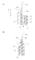
- the conventional microfluidic devices described in Patent Document 1 and Patent Document 2 are generally two substrates 101 and 102 like the microfluidic device 100 shown in FIG. A microchannel 103 formed by facing them, electrodes 104 and 105 for dielectrophoresis formed in the microchannel 103, and a liquid inlet formed by opening one substrate 102 106, a liquid outlet 107, and a side wall forming member 108.
- each of a large number of slits is configured as described above. Separation of different kinds of particles 120 existing in the fluid performed using the microfluidic device 100 is realized by trapping the particles 120 having a specific dielectric constant band between the electrodes 104 and 105.
- FIG. 18B shows an enlarged partial area AA of the microfluidic device 100 in which such stagnation occurs.
- the flow rate of the fluid 121 becomes slow in the stagnation region 110, so that the fluid stagnates and the particles 120 The pool can be made. If such particles can accumulate, the separation accuracy of the particles decreases. Further, when the number of trapped particles increases, the particles 120 newly flowing from behind collide with the trapped particles 120, and what is to be trapped is unintentionally pushed out and is separated (fractionation accuracy). May be reduced.
- An object of the present invention is to provide a microfluidic device and a dielectrophoresis apparatus suitable for accurately separating a large amount of particles.
- a microfluidic device includes an insulating sheet wound around a central axis and having a spiral shape in a cross section perpendicular to the central axis, a predetermined circumference of the insulating sheet, and A gap is provided between an insulating sheet disposed between the outer circumference and a predetermined circumference, and at least a part of the shape in a cross section perpendicular to the central axis is spiral and along the central axis And an electrode for forming an electric field which is formed on the insulating sheet and causes dielectrophoresis in the fluid flowing through the flow path.
- the occupation ratio of the spiral channel in the cross section of the wound insulating sheet is increased, and it is difficult to collect particles, and it is easy to separate a large amount of particles with high accuracy. Become.
- the microfluidic device has an inner wall along the outermost periphery of the insulating sheet, and further includes a hollow cylindrical case for flowing fluid through a spiral flow path from one opening to the other opening. May be.
- a hollow cylindrical case for flowing fluid through a spiral flow path from one opening to the other opening. May be.
- the microfluidic device may further include a funnel that is attached to the other opening of the case and collects the fluid that has passed through the flow path.
- a funnel that is attached to the other opening of the case and collects the fluid that has passed through the flow path.
- the electrode may include a voltage application electrode formed on the surface of the insulating sheet and a ground electrode formed in a rectangular shape on the back surface of the insulating sheet. In this case, it becomes easy to arrange the ground electrode at an appropriate position in the wound insulating sheet.
- the voltage application electrode may be a comb electrode having a plurality of comb teeth.
- the comb-shaped electrode is set in a range in which the extending direction of the plurality of comb teeth is inclined with respect to the direction orthogonal to the direction in which the flow path extends and the angle formed by the orthogonal direction is up to 45 degrees. It may be. In this case, even if there are already trapped particles between the comb electrodes, it will be easier for the particles that flow later to avoid the trapped particles and improve the accuracy when separating a large number of particles To do.
- the microfluidic device may further include a rod-shaped conductor shaft that is disposed on the innermost periphery of the insulating sheet along the central axis and is electrically connected to the ground electrode.
- the grounding electrode wound around the insulating sheet is easily grounded by the conductor shaft.
- the flow path may be formed in a region where the gap interval is constant except for the region where the gap interval between the beginning and end of winding of the insulating sheet changes.
- the height of the flow path can be made constant, the difference in flow velocity due to the height of the spiral flow path can be reduced, and high particle separation accuracy can be easily obtained.
- a dielectrophoresis device includes the above-described microfluidic device, a liquid feeding device for flowing a fluid to the microfluidic device, and a power supply unit for supplying power to the electrode. It is.
- a large amount of particles can be accurately separated in a microfluidic device.
- the same effect can be obtained in a dielectrophoresis apparatus including such a microfluidic device.
- the conceptual diagram which shows the outline
- inspection part of FIG. 1 is a perspective view showing an appearance of a microfluidic device according to a first embodiment.
- (b) The expanded sectional view of AC part of FIG. The typical sectional view of the transparent film for explaining the trap of particles.
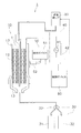
- FIG. 1 is a conceptual diagram of a configuration of a dielectrophoresis device according to the first exemplary embodiment of the present invention.
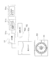
- FIG. 2 is a conceptual diagram for explaining the detection function of the dielectrophoresis device of the first embodiment.
- the dielectrophoresis apparatus 1 shown in FIG. 1 has a function of separating particles of the same kind by utilizing the difference in behavior of different particles in a fluid when an AC electric field is applied.
- the dielectrophoresis apparatus 1 includes a microfluidic device 10, a liquid feed pump 20, a sample recovery unit 30, a power supply unit 40, a detection unit 50, and a control device 60.
- a fluid flows from the liquid feed pump 20 through the microfluidic device 10 to the sample collection unit 30, and for this reason, the liquid feed pump 20, the microfluidic device 10, and the sample collection unit 30 include a liquid supply tube.
- the liquid feed pump 20 includes, for example, a syringe (not shown) filled with fluid. The syringe contains different kinds of particles to be separated together with the fluid.
- the liquid feed pump 20 can also be configured so that The sample collection unit 30 includes a first sample collection unit 31, a second sample collection unit 32, and a switching valve 33.
- the fluid flowing from the microfluidic device 10 is recovered by the first sample recovery unit 31 or the second sample recovery unit 32 according to the connection of the switching valve 33.
- the case where the fluid is recovered by the two first sample recovery units 31 and the second sample recovery unit 32 is shown, but there may be three or more sample recovery units.
- the power supply unit 40 includes a high frequency power supply 41 having a function of changing the frequency of the generated high frequency voltage and a ground terminal 42. Both the high frequency power supply 41 and the ground terminal 42 are connected to the electrodes of the microfluidic device 10. The connection between the power supply unit 40 and the microfluidic device 10 will be described in detail later.
- the detection unit 50 includes a detection device 51 and a detection probe 52. The type of detection device 51 and detection probe 52 to be used is appropriately selected according to the detection method and the like.
- FIG. 2 shows the configuration of the detection unit 50 in the case where particles flowing through the microfluidic device 10 are detected by optical detection. The detection unit 50 in FIG. 2 will be described later.
- the liquid feed pump 20, the sample collection unit 30, the power supply unit 40, and the detection unit 50 are controlled by the control device 60.
- the switching valve 33 is switched at an appropriate timing while automatically performing liquid feeding and detection, and desired particles are respectively collected in the first sample collecting unit 31 and the second sample collecting unit 32. Can do.
- FIG. 2 is a conceptual diagram for explaining an example of the configuration of the detection unit.
- a cross section of the microfluidic device 10 is shown.
- the microfluidic device 10 is fixed to a transparent holder 53, and is configured so that light is transmitted therethrough.
- the detection probe 52 includes an optical fiber 52a and a light source 52b in order to perform optical inspection.
- the light source 52b includes, for example, an LED (light emitting diode) that emits light to be applied to the optical fiber 52a. Light incident from the light source 52b is guided to the microfluidic device 10 through the optical fiber 52a, passes through the microfluidic device 10, and returns to the optical fiber 52a again.
- the light that has passed through the microfluidic device 10 enters the detection device 51 from the optical fiber 52a.
- the detection device 51 includes, for example, a spectroscope 51a, a fitting processing device 51b, and a monitor output device 51c.
- the light incident on the detection device 51 is split using, for example, a CCD (charge coupled device) of the spectroscope 51a.
- the fitting processing device 51b receives spectroscopic data from the spectroscope 51a.
- the monitor output device 51c receives the result of the fitting process from the fitting process device 51b and displays the detection result.
- the fitting processing device 51b identifies whether or not particles are trapped between the electrodes of the microfluidic device 10 based on a difference in peak shift of reflected light with respect to irradiation light obtained by, for example, spectral fitting processing. For example, by observing the wavelength change of the interference spectrum in the fitting processing device 51b, it is possible to detect a specific type of particles contained in the fluid.
- a CCD camera can be used as the detection probe 52, and a display device that enlarges and displays an image captured by the CCD camera can be used as the detection device 51.
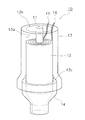
- FIG. 3 shows a state in which the microfluidic device 10 is viewed obliquely from above.
- the members constituting the microfluidic device 10 shown in FIG. 3 contain a cylindrical rod-shaped conductor shaft 11, an insulating transparent film 12 wound around the conductor shaft 11, and the transparent film 12.
- the case 13 is made of a heat-shrinkable material.
- PET polyethylene terephthalate
- the first electrode 15 and the second electrode 16 are formed on the surface side of the transparent film 12, and both the first electrode 15 and the second electrode 16 are made of a transparent conductive material. ing. As shown in FIGS. 4 and 5, the microfluidic device 10 further includes a ground electrode 17 and a spacer 18 formed on the back side of the transparent film 12. Similarly to the first electrode 15 and the second electrode 16, the ground electrode 17 is also formed of a conductive material having optical transparency and flexibility.
- the transparent film 12 is made of a transparent resin such as PET, polymethyl methacrylate (PMMA), polycarbonate (PC), and polyurethane. These resins have high insulating properties.
- the thickness of the transparent film 12 is preferably about 50 ⁇ m to 500 ⁇ m in consideration of winding to form a flow path.
- the transparent film 12 is used for optical detection by the detection unit 50. However, when performing detection by a method that does not use light, or when the detection unit 50 is not provided, dielectrophoresis is performed. In the case of an apparatus, an opaque insulating sheet can also be used.
- the transparent film 12 is provided with electrode extraction portions 12a and 12b for connecting the first electrode 15 and the second electrode 16 to external wirings, respectively.
- Electrode extraction portions 12a and 12b are formed in the electrode lead portions 12a and 12b, respectively.
- the direction of arrow AW1 in FIG. 4 is the direction in which the fluid flows, that is, the direction of the flow path. Since the electrode extraction portions 12a and 12b extend long in the direction in which the fluid flows, the electrode extraction portions 12a and 12b can be configured to protrude outward from the upper end portion of the cylinder when the transparent film 12 is wound around the cylinder.
- the first electrode 15, the second electrode 16, and the ground electrode 17 are carbon nanotubes (CNT) having light transmittance and flexibility in the first embodiment for the same reason as the transparent film 12. It is formed of poly 3,4-ethylenedioxythiophene (PEDOT), metal nanofiber, metal mesh, thin film plating, and the like. Examples of the metal herein include copper (Cu), silver (Ag), aluminum (Al), and gold (Au).
- the first electrode 15 and the second electrode 16 are a pair of comb-shaped electrodes in which comb teeth 15 a and 16 a are arranged alternately.
- the comb teeth 15a and 16a of the first electrode 15 and the second electrode 16 shown in FIG. 4 extend in a direction orthogonal to the flow path.
- the comb teeth 15a and 16a are arranged so as to be orthogonal to the arrow AW1 that is the direction in which the fluid flows.
- the back side of the transparent film 12 on which the ground electrode 17 is formed is wound inside when the transparent film 12 is wound. That is, the surface side on which the pair of first electrode 15 and second electrode 16 is formed appears outside the cylinder.
- the spacer 18 is an insulator.
- the spacer 18 is designed in the shape of, for example, a cylinder, a sphere, a dome, or a quadrangular column.
- the height of the spacer 18 is preferably set to 100 ⁇ m to 500 ⁇ m, for example.
- the arrangement of the spacers 18 can be, for example, a staggered arrangement as shown in FIG.
- the horizontal pitch Pc and the vertical pitch Pl in the staggered arrangement are preferably set within a range of 0.5 mm to 3 mm, for example.
- the spacer 18 As the material of the spacer 18, PET, PMMA, PC, acrylonitrile butadiene styrene (ABS), polydimethylsiloxane (PDMS), polyimide (PI), polyether ether ketone (PEEK), resist, and the like are used.
- the spacer 18 may be transparent or opaque.
- FIG. 7 is a flowchart showing an outline of the manufacturing process of the microfluidic device 10.
- an electrode patterning step S1 in which the first electrode 15, the second electrode 16, and the ground electrode 17 shown in FIGS. 4 and 5 are formed is performed.
- the patterning of the electrodes is continuously performed using a long transparent film 80 (see FIG. 8A), which is a material of the transparent film 12, on which metal foil is formed on both sides.
- the metal foil is etched to pattern the metal foil into a shape as shown in FIGS.
- the spacers 18 shown in FIGS. 5 and 6 are formed using a method using a spacer film, a method for patterning a photoresist, a method for arranging dot spacers, and the like. A method using a spacer film among these will be described later. These methods can also be performed continuously on the long transparent film 80.
- the outer shape of the long transparent film 80 on which the first electrode 15, the second electrode 16, the ground electrode 17, and the spacer 18 are formed is cut (film outer shape cutting step S3). By this cutting, the transparent film 12 having a rectangular planar shape is formed.
- the conductor shaft 11 is bonded along one side of the transparent film 12 (axis / film bonding step S4). After the adhesion between the conductor shaft 11 and the transparent film 12 is completed, for example, after the adhesive is dried, the transparent film 12 is wound around the conductor shaft 11 in a scroll shape (film winding step S5). Finally, the transparent film 12 wound around the conductor shaft 11 is incorporated into the cylindrical case 13 (case incorporation step S6).
- the assembly of the microfluidic device including the film winding step S5 and the case incorporation step S6 will be described later.
- FIG. 8A shows a long spacer film on a long transparent film 80 on which the first electrode 15, the second electrode 16 and the ground electrode 17 are formed.
- 81 is bonded.
- the spacer film 81 is half-cut so that the portion that becomes the spacer 18 and the other portion can be separated by the die-cut roll 82.
- the unnecessary portion 81a of the long spacer film 81 is removed, and the spacer 18 remains on the long transparent film 80 (see FIG. 8C).
- the long transparent film 80 from which the unnecessary portion 81a has been removed is wound into a roll and stored. Then, when the microfluidic device 10 is manufactured, a necessary number of transparent films 12 are cut out from the long transparent film 80.
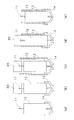
- FIGS. 9A to 9E show an assembly process of the microfluidic device 10.
- the cylindrical transparent film 12 wound around the conductor shaft 11 is first fitted into the funnel 14 at its lower end as shown in FIG.
- the cylindrical guide 85 shown in FIG. 9B is fitted into the upper end of the conductor shaft 11.
- the outer diameter of the cylindrical guide 85 is set to be the same as the outer diameter of the cylindrical transparent film 12 or slightly larger than the outer diameter of the transparent film 12.
- the outer diameter of the guide 85 is set to be equal to or smaller than the outer diameter of the funnel 14.
- the hollow cylindrical case 13 is fitted to the outer periphery of the funnel 14 through the outside of the guide 85 (see FIG. 9C).
- the inner diameter of the case 13 is set larger than the outer diameter of the funnel 14 so that the case 13 fits into the funnel 14. Since the case 13 is formed of a material that contracts by heat, the case 13 contracts by heating the whole in the state of FIG. 9C, and the state shown in FIG. 9D is obtained. . In order to stop the heating so as to be in the state of FIG. 9D, for example, the timing of stopping the heating is taken on the basis of the case where the outer diameter of the case 13 coincides with the outer diameter of the guide 85. When the heating is stopped and the contraction of the case 13 stops, the guide 85 is removed from the conductor shaft 11 to complete the assembly of the microfluidic device 10 (see FIG. 9E).
- the case 13 is thermally shrunk so that the inner wall of the case 13 is in close contact with the outermost periphery of the transparent film 12, and the inner wall of the case 13 is fixed on the outer periphery of the funnel 14. Is supported and the funnel 14 and the transparent film 12 are fixed.
- the conductor shaft 11 is placed on the ground electrode 17 coated with, for example, a conductive adhesive.
- the conductor shaft 11 is wound around the ground electrode 17 only once in the direction of the arrow AW2. Therefore, the adhesive region Ar ⁇ b> 1 on the axial center side of the transparent film 12 has the same length as the outer periphery of the conductor shaft 11.
- the spacer 18 is not disposed in the bonding region Ar ⁇ b> 1 in order to make electrical connection between the conductor shaft 11 and the ground electrode 17.
- the transparent film 12 when the transparent film 12 is wound around the conductor shaft 11, a gap having a constant interval is formed between an arbitrary circumference and an outer circumference by the spacer 18 except for the winding start and the winding end.
- This gap becomes the flow path 2.
- the flow path 2 extends toward the central axis direction in which the conductor shaft 11 extends.
- the transparent film 12 With this flow path 2, the transparent film 12 becomes spiral in a cross section perpendicular to the longitudinal direction of the conductor shaft 11 (cross section perpendicular to the central axis) (see FIG. 12). That is, the flow path 2 also has a spiral cross-sectional shape.
- 12 is a cross-sectional view taken along the line II of FIG. Referring to FIGS.
- transparent spacers 19a and 19b having a wedge-shaped cross section are inserted at the start and end of winding.
- the transparent film 12 is wound around the conductor shaft 11
- the wedge-shaped spacers 19a and 19b are wound together.
- the fluid flows through the flow path region Ar2 in FIG.
- the fact that such a spacer 19a, 19b prevents fluid from flowing where the gap between the winding start and winding ends is not constant means that the height of the flow path is constant.
- uniform particle separation can be performed by dielectrophoresis, which improves the accuracy of particle analysis and particle fractionation.
- dielectrophoresis there is dielectrophoresis in which, for example, a suspension in which several types of particles are mixed is separated using a difference in dielectric constant of the particles.
- FIG. 13A is an enlarged cross-sectional view schematically showing a partial area AB of the microfluidic device 10 shown in FIG. 12, and FIG. 13B shows another area AC of the microfluidic device 10. It is an expanded sectional view showing typically.
- the high frequency power supply 41 of the power supply unit 40 has one power supply terminal 41a connected to the lead-out part 15b and the other power supply terminal 41b connected to the lead-out part 16b.
- the conductor shaft 11 is connected to the ground terminal 42 of the power supply unit 40.
- one of the two different types of particles 3a and 3b becomes the first particle 3a. It is trapped between the first electrode 15 and the second electrode 16, and the other particle 3b flows through the flow path 2 without being trapped.
- the curve drawn between the first electrode 15 and the second electrode 16 represents an electric field
- the arrow AW3 represents the direction in which the fluid flows.
- the microfluidic device and the dielectrophoresis apparatus according to the second embodiment of the present invention are the same as the microfluidic device 10 and the dielectrophoresis apparatus 1 of the first embodiment except for the form of electrodes.
- the microfluidic device 10 of the first embodiment has two comb-shaped electrodes of the first electrode 15 and the second electrode, whereas the microfluidic device of the second embodiment has only one comb-shaped electrode. Not different. Therefore, in the following, the transparent film and electrodes of the microfluidic device of the second embodiment will be described, and description of other configurations will be omitted.
- FIG. 15A schematically shows the transparent film and electrode of the second embodiment.
- the configuration of the microfluidic device 10A other than the transparent film 12A and the comb-shaped electrode 15A is the same as that of the microfluidic device 10, and is not shown in FIG.
- the transparent film 12A is formed of the same material as the transparent film 12 of the first embodiment and has the same thickness.
- an opaque insulating sheet Can be used as in the first embodiment, in the second embodiment as well, in the case where detection is performed by a method that does not use light in the detection unit 50 or in the case of a dielectrophoresis apparatus that does not include the detection unit 50.
- One electrode extraction part 12Aa is provided in the transparent film 12A.
- the comb electrode 15A is connected to one power supply terminal 41a of the high frequency power supply 41 of the power supply section 40A shown in FIG. 15B, and the ground electrode 17A is connected to the other power supply terminal 41b of the high frequency power supply 41. Connected.
- the other power supply terminal 41 b is connected to the ground terminal 42.
- Such a dielectrophoresis apparatus 1A of the second embodiment can be configured in the same manner as the dielectrophoresis apparatus 1 of the first embodiment except for the configuration of the power supply unit 40A.
- FIG. 15B the configuration of the dielectrophoresis apparatus 1A other than the power supply unit 40A, the conductor shaft 11, the transparent film 12A, and the comb-shaped electrode 15A is the same as that of the dielectrophoresis apparatus 1, and is not shown.
- FIG. 16 shows a state where different kinds of particles are separated inside the microfluidic device 10A.
- the arrow AW4 is the direction in which the fluid flows.
- a high-frequency electric field is generated between the comb electrode 15A and the ground electrode 17A. In the high frequency electric field shown in FIG. 16, the particles 3c are trapped and the particles 3d pass through the flow path 2A. When the frequency of the high-frequency electric field changes, the trap of the particles 3c can be released.
- the transparent films 12 and 12A are wound around the central axis, and the shape in a cross section perpendicular to the central axis is spiral as shown in FIG. It is. Further, as shown in FIG. 12 and the like, for example, the transparent film disposed between the predetermined circumference r1 of the transparent films 12 and 12A and the outer circumference r2 and located on the predetermined circumference r1 and the outer circumference r2. A spacer 18 is arranged between the two and a gap is provided.
- This gap is the flow path 2, 2 ⁇ / b> A, and the flow path 2, 2 ⁇ / b> A has a spiral shape in a cross section perpendicular to the conductor shaft 11, that is, a cross section perpendicular to the central axis, and extends along the central axis. .
- Almost all of the inner circumference of the cross section of the case 13 of the cylindrical microfluidic devices 10 and 10A except for the thin transparent films 12 and 12A and the area occupied by the conductor shaft are the spiral flow paths 2 and 2A. Since the occupation ratio of the spiral channel in the cross section of the films 12 and 12A is increased, it becomes easy to separate a large amount of particles with high accuracy.
- the electrodes of the microfluidic devices 10 and 10A include a first electrode 15 and a second electrode 16 formed on the surface of the transparent films 12 and 12A, a comb-shaped electrode 15A (an example of a voltage application electrode), and the transparent films 12 and 12A.
- a ground electrode 17 which is formed in a rectangular shape on the back surface. In this case, in the transparent films 12 and 12A wound in a scroll shape, the electric fields of the first electrode 15 and the second electrode 16 of the adjacent flow paths 2 and 2A as shown in FIG.
- the ground electrode 17 can be shielded by the ground electrode 17, and the ground electrode 17 can be easily disposed at an appropriate position.
- the pair of first electrodes 15B (examples of comb-shaped electrodes) and second electrodes 16B (examples of comb-shaped electrodes) are arranged such that the extending directions of the comb teeth 15Ba and 16Ba are alternately arranged.
- the angle between the direction perpendicular to the direction in which the flow path extends (the direction of the arrow AW5) and the direction orthogonal to the direction that is orthogonal is set in a range of up to 45 degrees (the direction of the arrow AW6).
- the direction in which the comb teeth 15a and 16a extend will be described in more detail.
- the direction of arrow AW7 in FIG. 17 is the direction orthogonal to the direction in which the flow path extends (direction of arrow AW5).
- the direction inclined by ⁇ degrees from the direction of the arrow AW7 is the direction of the arrow AW8.
- the inclination angle ⁇ is preferably 45 degrees or less. That is, since the angle between the direction of the arrow AW6 and the direction orthogonal to the direction is 45 degrees, the direction with the arrow AW8 is preferable with the direction of the arrow AW6 as the boundary, and the direction with the arrow AW9 is not preferable. . Also in the case of the comb-shaped electrode 15A shown in FIG. 15, the extending direction of the comb teeth 15Aa may be inclined similarly to the comb teeth 15Ba and 16Ba.
- the conductor shaft 11 of the microfluidic devices 10 and 10A is disposed on the innermost circumference of the transparent films 12 and 12A along the central axis, and is electrically connected to the ground electrodes 17 and 17A. Therefore, if the conductor shaft 11 is connected to the ground terminal 42 of the power supply unit 40, the ground electrodes 17 and 17A can be grounded, and the ground electrodes 17 and 17A wound around the insulating transparent films 12 and 12A can be easily grounded.
- the dielectrophoresis apparatus 1, 1 ⁇ / b> A includes the above-described microfluidic devices 10, 10 ⁇ / b> A, and a liquid feed pump 20 (an example of a liquid feed apparatus) for flowing a fluid to the microfluidic devices 10, 10 ⁇ / b> A, and power to the electrodes Since the power supply unit 40 is supplied to the dielectrophoresis apparatuses 1 and 1A, a large amount of particles can be accurately separated.
- the hollow cylindrical case 13 has an inner wall 13a along the outermost periphery of the transparent films 12 and 12A.
- the case 13 is configured such that a fluid flows through the flow paths 2 and 2A from one opening 13b of the case 13 toward the other opening 13c.
- the fluid can be guided to the flow paths 2 and 2A, so that a large amount of fluid can be easily passed through the microfluidic devices 10 and 10A. Separation of a large amount of particles becomes easy.
- the flow paths 2 and 2A are configured so that the fluid does not flow to the winding start and winding end portions by the wedge-shaped spacers 19a and 19b. That is, the gap interval is formed in a constant region except for the region where the gap interval between the winding start and the winding end of the transparent films 12 and 12A changes. In this case, since the heights of the flow paths 2 and 2A can be made uniform, the difference in flow velocity due to the height of the spiral flow paths 2 and 2A can be reduced, and high particle separation accuracy can be easily obtained. .
- the flow path 2 demonstrated the case where it was the shape connected in the spiral shape in the cross section perpendicular
- the fluid flow in the direction along the spiral may be limited by, for example, a rib extending along the central axis, and the fluid flow along the central axis direction may be adjusted.
- the flow path 2 is comprised using the surface side and back surface side of one transparent film 12 and 12A.
- one transparent film 12 and 12A it is preferable to use a single transparent film 12, 12A because less material is required.
- two insulating sheets may be separately arranged on the front surface side and the back surface side, respectively, and they may be wound in a scroll shape to form a spiral cross-sectional flow path.
- the insulation sheet is not limited to a single sheet.
- the transparent wedge-shaped spacers 19a and 19b are inserted at the start and end of winding of the transparent films 12 and 12A.
- the spacers 19a and 19b are inserted.
- the configuration in which the fluid does not flow in the region is not limited to this.
- a wall that shields this portion may be provided, and the region where the gap between the winding start and the winding end changes may be a hollow space separated from the flow path 2.
- the wall for forming the hollow space is transparent, detection light can be transmitted.
- the case 13 is cylindrical and the outermost periphery of the transparent films 12 and 12A is cylindrical.
- the inner wall 13a of the case 13 and the transparent films 12 and 12A The outermost cross-sectional shape is not limited to a circle. For example, it may be a square or a polygon other than a square.
- the dielectrophoresis apparatuses 1 and 1A including the detection unit 50 have been described.
- the dielectrophoresis apparatus according to the present invention may be simply used as a fractionation apparatus without providing the detection unit. it can.
- the first embodiment and the second embodiment of the present invention have been described above, the present invention is not limited to the above-described embodiment, and various modifications can be made without departing from the scope of the invention. In particular, a plurality of embodiments and modifications described in this specification can be arbitrarily combined as necessary.
Landscapes
- Chemical & Material Sciences (AREA)
- Health & Medical Sciences (AREA)
- Life Sciences & Earth Sciences (AREA)
- General Health & Medical Sciences (AREA)
- Molecular Biology (AREA)
- Chemical Kinetics & Catalysis (AREA)
- Analytical Chemistry (AREA)
- Electrochemistry (AREA)
- Microelectronics & Electronic Packaging (AREA)
- General Physics & Mathematics (AREA)
- Hematology (AREA)
- Engineering & Computer Science (AREA)
- Dispersion Chemistry (AREA)
- Physics & Mathematics (AREA)
- Biochemistry (AREA)
- Clinical Laboratory Science (AREA)
- Immunology (AREA)
- Pathology (AREA)
- Physical Or Chemical Processes And Apparatus (AREA)
- Electrostatic Separation (AREA)
- Sampling And Sample Adjustment (AREA)
- Investigating Or Analysing Materials By Optical Means (AREA)
- Investigating Or Analyzing Materials By The Use Of Electric Means (AREA)
- Micromachines (AREA)
Abstract
【課題】大量の粒子を精度よく分離するのに適したマイクロ流体デバイス及び誘電泳動装置を提供する。 【解決手段】マイクロ流体デバイス10は、絶縁性の透明フィルム12とスペーサ18と第1電極、第2電極及び接地電極を備えている。透明フィルム12は、導体軸11、つまり中心軸の周りに巻回され、中心軸に垂直な断面における形状が渦巻状である。スペーサ18によって、透明フィルム12の所定の周とその外側の周との間に配置されて所定の周と外側の周にある透明フィルム12の間に隙間が設けられる。スペーサ18による隙間で、中心軸に垂直な断面における形状が渦巻状であって中心軸に沿って延びる流路2が形成される。第1電極、第2電極及び接地電極は透明フィルム12上に形成されており、これら電極に高周波電圧が印加されることによって流路2を流れる流体内で誘電泳動が生じる。
Description
本発明は、マイクロ流体デバイス及びマイクロ流体デバイスを使用する誘電泳動装置に関する。
近年、経済性や環境保護の観点から、ガラスなどの小さな基板に微細な溝や空洞を形成し、化学反応、細胞培養、分離検出等のプロセスに用いる粒子などの量をできるだけ減らすことが試みられている。このようなプロセスに用いられるマイクロ流体デバイスとして、例えば、特許文献1(特開2006-26791号公報)には、厚さ1mmのガラス基板の上に、幅及び高さが各200μm、長さが50mmの微細流路を持つマイクロ流体デバイスが記載されている。
また、特許文献2には、このようなラボオンアチップ(Lab-on-a-chip)の大量生産を可能にするため、1枚の樹脂フィルムを打ち抜いてスリットを形成し、このスリットが形成されている部分を他の2枚の樹脂フィルムで挟むマイクロ流体デバイスの製造方法が開示されている。この特許文献2には、単に3枚の樹脂フィルムのサンドイッチ構造でラボオンアチップを形成するだけでなく、複数のスリットを有するサンドイッチ構造の樹脂フィルムを巻き取ることにより、ロール状に形成されたラボオンアチップを得る技術が示されている。
また、特許文献2には、このようなラボオンアチップ(Lab-on-a-chip)の大量生産を可能にするため、1枚の樹脂フィルムを打ち抜いてスリットを形成し、このスリットが形成されている部分を他の2枚の樹脂フィルムで挟むマイクロ流体デバイスの製造方法が開示されている。この特許文献2には、単に3枚の樹脂フィルムのサンドイッチ構造でラボオンアチップを形成するだけでなく、複数のスリットを有するサンドイッチ構造の樹脂フィルムを巻き取ることにより、ロール状に形成されたラボオンアチップを得る技術が示されている。
ところで、特許文献1や特許文献2に記載されている従来のマイクロ流体デバイスは、一般的に、図18(a)に示されているマイクロ流体デバイス100のように、2枚の基板101,102と、それらを対向させて形成された微細流路103と、微細流路103に形成されている誘電泳動用の電極104,105と、一方の基板102を開口させて形成されている液流入口106及び液流出口107と側壁形成部材108とを備えている。特許文献2のロール状に形成されたラボオンアチップも多数のスリットの各々は、前述のような構成になっている。
このようなマイクロ流体デバイス100を使って行われる、流体内に存在する異種の粒子120の分離は、特定の誘電率帯の粒子120を電極104,105間に引き付けるなどしてトラップすることで実現される。電極104,105間が粒子で埋め尽くされる(飽和する)と、それ以上粒子120をトラップできず、粒子の分離が行われなくなる。そこで、分離能力を向上させるには電極面積を拡大させるのが有効であることが分かる。しかし、そのためには微細流路103を大きくせざるを得ず、従来のマイクロ流体デバイス100の構造は、大量の粒子を処理するということには不向きである。
また、微細流路103に高低差があると、そこに流体のよどみが発生し、粒子120が滞留、粒子の回収率が低下してしまう。例えば、図18(b)には、このようなよどみが発生するマイクロ流体デバイス100の一部領域AAが拡大されて示されている。誘電泳動の対象となっている粒子120が矢印122の方向に流れている流体121によって移動している状態において、よどみ領域110では、流体121の流速が遅くなるため、流体がよどんで粒子120の溜りができてしまう。このような粒子の溜りができると、粒子の分離精度が低下する。
さらに、トラップする粒子数が多くなると、トラップされている粒子120に後方から新たに流れてくる粒子120が衝突し、トラップされるべきものが意図せずに押し出されて分離精度(分留精度)が低下してしまう可能性がある。
このようなマイクロ流体デバイス100を使って行われる、流体内に存在する異種の粒子120の分離は、特定の誘電率帯の粒子120を電極104,105間に引き付けるなどしてトラップすることで実現される。電極104,105間が粒子で埋め尽くされる(飽和する)と、それ以上粒子120をトラップできず、粒子の分離が行われなくなる。そこで、分離能力を向上させるには電極面積を拡大させるのが有効であることが分かる。しかし、そのためには微細流路103を大きくせざるを得ず、従来のマイクロ流体デバイス100の構造は、大量の粒子を処理するということには不向きである。
また、微細流路103に高低差があると、そこに流体のよどみが発生し、粒子120が滞留、粒子の回収率が低下してしまう。例えば、図18(b)には、このようなよどみが発生するマイクロ流体デバイス100の一部領域AAが拡大されて示されている。誘電泳動の対象となっている粒子120が矢印122の方向に流れている流体121によって移動している状態において、よどみ領域110では、流体121の流速が遅くなるため、流体がよどんで粒子120の溜りができてしまう。このような粒子の溜りができると、粒子の分離精度が低下する。
さらに、トラップする粒子数が多くなると、トラップされている粒子120に後方から新たに流れてくる粒子120が衝突し、トラップされるべきものが意図せずに押し出されて分離精度(分留精度)が低下してしまう可能性がある。
本発明の課題は、大量の粒子を精度よく分離するのに適したマイクロ流体デバイス及び誘電泳動装置を提供することにある。
以下に、課題を解決するための手段として複数の態様を説明する。これら態様は、必要に応じて任意に組み合せることができる。
本発明の一見地に係るマイクロ流体デバイスは、中心軸の周りに巻回され、中心軸に垂直な断面における形状の少なくとも一部が渦巻状である絶縁シートと、絶縁シートの所定の周とその外側の周との間に配置されて所定の周と外側の周にある絶縁シートの間に隙間を設け、中心軸に垂直な断面における形状の少なくとも一部が渦巻状であって中心軸に沿って延びる流路を形成するスペーサと、絶縁シート上に形成され、流路を流れる流体内で誘電泳動を生じさせる電界を形成するための電極と、を備えるものである。
このように構成されたマイクロ流体デバイスでは、巻かれた絶縁シートの断面に占める渦巻状の流路の占有割合が大きくなるとともに粒子の溜りなどができ難くなり、大量の粒子を精度よく分離し易くなる。
本発明の一見地に係るマイクロ流体デバイスは、中心軸の周りに巻回され、中心軸に垂直な断面における形状の少なくとも一部が渦巻状である絶縁シートと、絶縁シートの所定の周とその外側の周との間に配置されて所定の周と外側の周にある絶縁シートの間に隙間を設け、中心軸に垂直な断面における形状の少なくとも一部が渦巻状であって中心軸に沿って延びる流路を形成するスペーサと、絶縁シート上に形成され、流路を流れる流体内で誘電泳動を生じさせる電界を形成するための電極と、を備えるものである。
このように構成されたマイクロ流体デバイスでは、巻かれた絶縁シートの断面に占める渦巻状の流路の占有割合が大きくなるとともに粒子の溜りなどができ難くなり、大量の粒子を精度よく分離し易くなる。
マイクロ流体デバイスは、絶縁シートの最外周に沿う内壁を有し、一方の開口部から他方の開口部に向けて渦巻状の流路を通して流体を流すための中空筒状のケースをさらに備えて構成されてもよい。
このように構成されたマイクロ流体デバイスでは、一方の開口部から他方の開口部に向けてケース内に流体を流すことによって、流路に流体を導けるので大量の流体をマイクロ流体デバイスに通しやすくなり、大量の粒子の分離が容易になる。
このように構成されたマイクロ流体デバイスでは、一方の開口部から他方の開口部に向けてケース内に流体を流すことによって、流路に流体を導けるので大量の流体をマイクロ流体デバイスに通しやすくなり、大量の粒子の分離が容易になる。
マイクロ流体デバイスは、ケースの他方の開口部に取り付けられ、流路を通過した流体を回収するための漏斗をさらに備えてもよい。
このように構成されたマイクロ流体デバイスでは、流路を通過した流体の回収が漏斗によって容易になる。
このように構成されたマイクロ流体デバイスでは、流路を通過した流体の回収が漏斗によって容易になる。
電極は、絶縁シートの表面に形成されている電圧印加電極と、絶縁シートの裏面に矩形状に形成されている接地電極とを含むものであってもよい。
この場合、巻回された絶縁シートにおいて、適切な位置に接地電極を配置し易くなる。
この場合、巻回された絶縁シートにおいて、適切な位置に接地電極を配置し易くなる。
電圧印加電極は、複数の櫛歯を有する櫛型電極であってもよい。この場合、粒子をトラップする箇所を増やすことができ、大量の粒子を分離し易くなる。
櫛型電極は、複数の前記櫛歯の延びる方向が、流路の延びる方向に対して直交する向きよりも傾斜した向きであって直交する向きとのなす角が45度までの範囲で設定されていてもよい。この場合、櫛型電極の間に既にトラップされている粒子があっても、後から流れてくる粒子がトラップされている粒子を避けて通りやすくなり、大量の粒子を分離するときの精度が向上する。
櫛型電極は、複数の前記櫛歯の延びる方向が、流路の延びる方向に対して直交する向きよりも傾斜した向きであって直交する向きとのなす角が45度までの範囲で設定されていてもよい。この場合、櫛型電極の間に既にトラップされている粒子があっても、後から流れてくる粒子がトラップされている粒子を避けて通りやすくなり、大量の粒子を分離するときの精度が向上する。
マイクロ流体デバイスは、中心軸に沿って絶縁シートの最内周に配置され、接地電極に電気的に接続されている棒状の導体軸をさらに備えるものであってもよい。
このように構成されたマイクロ流体デバイスでは、導体軸によって、絶縁シートに巻き込まれる接地電極の接地が容易になる。
このように構成されたマイクロ流体デバイスでは、導体軸によって、絶縁シートに巻き込まれる接地電極の接地が容易になる。
流路は、絶縁シートの巻き始めと巻き終わりの隙間の間隔が変化する領域を除いた隙間の間隔が一定の領域に形成されているものであってもよい。
この場合、流路の高さを一定に揃えることができるので、渦巻状の流路の高さに起因する流速の差を小さくでき、高い粒子の分離精度を得やすくなる。
この場合、流路の高さを一定に揃えることができるので、渦巻状の流路の高さに起因する流速の差を小さくでき、高い粒子の分離精度を得やすくなる。
本発明の一見地に係る誘電泳動装置は、上述のマイクロ流体デバイスと、マイクロ流体デバイスに対して流体を流すための送液装置と、電極に電力を供給するための電源部と、を備えるものである。
本発明によれば、マイクロ流体デバイスにおいて、大量の粒子を精度よく分離することができる。また、このようなマイクロ流体デバイスを備える誘電泳動装置においても同様の効果を奏する。
<第1実施形態>
(1)誘電泳動装置の構成の概要
図1及び図2を用いて、マイクロ流体デバイスを使用する誘電泳動装置の構成の概要について説明する。図1は、本発明の第1実施形態に係る誘電泳動装置の構成の概念図である。図2は、第1実施形態の誘電泳動装置の検出機能を説明するための概念図である。図1に示されている誘電泳動装置1は、交流電界を掛けたときの異種粒子の流体中の挙動の差異を利用して、同種の粒子ごとに分離する機能を有している。そのために、誘電泳動装置1は、マイクロ流体デバイス10と、送液ポンプ20と、サンプル回収部30と、電源部40と、検出部50と、制御デバイス60とを備えている。このような誘電泳動装置1は、送液ポンプ20からマイクロ流体デバイス10を通ってサンプル回収部30に流体が流れ、そのために送液ポンプ20とマイクロ流体デバイス10とサンプル回収部30が送液チューブ(図示せず)で接続されている。
送液ポンプ20は、例えば、流体が充填されているシリンジ(図示せず)を含んでいる。シリンジには、流体と一緒に、分離対象の異種の粒子が入っている。そして、このシリンジによって流体に一定の圧力が加えられ、流体がマイクロ流体デバイス10からサンプル回収部30の各部において一定の流速で流れる。また、シリンジには粒子が入っているので、粒子が、流体の流れに乗ってマイクロ流体デバイス10を通ってサンプル回収部30に運ばれる。ここでは、送液ポンプ20のシリンジが流体供給機能と粒子供給機能の2つの機能を兼用する場合について説明したが、これらの機能を異なる機器に分担して流体と粒子を別の機器からそれぞれ供給させるように送液ポンプ20を構成することもできる。
サンプル回収部30は、第1サンプル回収部31と第2サンプル回収部32と切換バルブ33とを有している。マイクロ流体デバイス10から流れてくる流体は、切換バルブ33の接続に応じて、第1サンプル回収部31又は第2サンプル回収部32に回収される。ここでは、流体を2つの第1サンプル回収部31と第2サンプル回収部32で回収する場合について示しているが、サンプル回収部は3つ以上あってもよい。
(1)誘電泳動装置の構成の概要
図1及び図2を用いて、マイクロ流体デバイスを使用する誘電泳動装置の構成の概要について説明する。図1は、本発明の第1実施形態に係る誘電泳動装置の構成の概念図である。図2は、第1実施形態の誘電泳動装置の検出機能を説明するための概念図である。図1に示されている誘電泳動装置1は、交流電界を掛けたときの異種粒子の流体中の挙動の差異を利用して、同種の粒子ごとに分離する機能を有している。そのために、誘電泳動装置1は、マイクロ流体デバイス10と、送液ポンプ20と、サンプル回収部30と、電源部40と、検出部50と、制御デバイス60とを備えている。このような誘電泳動装置1は、送液ポンプ20からマイクロ流体デバイス10を通ってサンプル回収部30に流体が流れ、そのために送液ポンプ20とマイクロ流体デバイス10とサンプル回収部30が送液チューブ(図示せず)で接続されている。
送液ポンプ20は、例えば、流体が充填されているシリンジ(図示せず)を含んでいる。シリンジには、流体と一緒に、分離対象の異種の粒子が入っている。そして、このシリンジによって流体に一定の圧力が加えられ、流体がマイクロ流体デバイス10からサンプル回収部30の各部において一定の流速で流れる。また、シリンジには粒子が入っているので、粒子が、流体の流れに乗ってマイクロ流体デバイス10を通ってサンプル回収部30に運ばれる。ここでは、送液ポンプ20のシリンジが流体供給機能と粒子供給機能の2つの機能を兼用する場合について説明したが、これらの機能を異なる機器に分担して流体と粒子を別の機器からそれぞれ供給させるように送液ポンプ20を構成することもできる。
サンプル回収部30は、第1サンプル回収部31と第2サンプル回収部32と切換バルブ33とを有している。マイクロ流体デバイス10から流れてくる流体は、切換バルブ33の接続に応じて、第1サンプル回収部31又は第2サンプル回収部32に回収される。ここでは、流体を2つの第1サンプル回収部31と第2サンプル回収部32で回収する場合について示しているが、サンプル回収部は3つ以上あってもよい。
電源部40は、発生する高周波電圧の周波数を変更する機能を有する高周波電源41と接地端子42とを有する。これら高周波電源41も接地端子42もマイクロ流体デバイス10の電極に接続される。この電源部40とマイクロ流体デバイス10との接続については後ほど詳しく説明する。
検出部50は、検出デバイス51と検出プローブ52とを有する。これら検出デバイス51と検出プローブ52にどのような種類のものを用いるかは、検出方法などに応じて適宜選択される。図2には、光学的な検出によってマイクロ流体デバイス10を流れる粒子の検出を行う場合の検出部50の構成が示されているが、図2の検出部50についての説明は後ほど行う。
上述の送液ポンプ20とサンプル回収部30と電源部40と検出部50は、制御デバイス60によって制御される。それにより、例えば、自動的に、送液を行って検出を行いながら適切なタイミングで切換バルブ33を切り換え、第1サンプル回収部31と第2サンプル回収部32にそれぞれ所望の粒子を回収することができる。
検出部50は、検出デバイス51と検出プローブ52とを有する。これら検出デバイス51と検出プローブ52にどのような種類のものを用いるかは、検出方法などに応じて適宜選択される。図2には、光学的な検出によってマイクロ流体デバイス10を流れる粒子の検出を行う場合の検出部50の構成が示されているが、図2の検出部50についての説明は後ほど行う。
上述の送液ポンプ20とサンプル回収部30と電源部40と検出部50は、制御デバイス60によって制御される。それにより、例えば、自動的に、送液を行って検出を行いながら適切なタイミングで切換バルブ33を切り換え、第1サンプル回収部31と第2サンプル回収部32にそれぞれ所望の粒子を回収することができる。
(2)検出部の概観
図2は、検出部の構成の一例を説明するための概念図である。この図2には、マイクロ流体デバイス10の断面が示されている。マイクロ流体デバイス10は、透明のホルダー53に固定されており、その中を光が透過するように構成されている。
図2に示されている検出部50は、光学検査を行うために、検出プローブ52が光ファイバ52aと光源52bで構成されている。光源52bは、光ファイバ52aに与える光を発する例えばLED(発光ダイオード)を有している。光源52bから入射した光は、光ファイバ52aを通してマイクロ流体デバイス10に導かれ、マイクロ流体デバイス10の中を通過して再び光ファイバ52aに戻る。マイクロ流体デバイス10の中を通過した光は、光ファイバ52aから検出デバイス51に入射する。
検出デバイス51は、例えば分光器51aとフィッティング処理デバイス51bとモニタ出力デバイス51cとで構成される。検出デバイス51に入射した光は、例えば分光器51aのCCD(電荷結合素子)を使って分光される。フィッティング処理デバイス51bは、分光器51aから分光に関するデータを受信する。モニタ出力デバイス51cは、フィッティング処理デバイス51bからフィッティング処理の結果を受信して検出結果を表示する。フィッティング処理デバイス51bは、例えば分光フィッティング処理により得られる照射光に対する反射光のピークシフトの違いから、マイクロ流体デバイス10の電極間に粒子がトラップされているか否かを識別する。例えば、フィッティング処理デバイス51bにおいて干渉スペクトルの波長変化を観測することで、流体中に含まれている特定種類の粒子を検出することができる。
また、検出部50の他の例としては、検出プローブ52にCCDカメラを用い、検出デバイス51としてCCDカメラが捕らえた映像を拡大して表示する表示装置を用いることができる。このような構成を用いれば、例えばマイクロ流体デバイス10に捕集された細胞の様子を高倍率のCCDカメラを使って観察することができる。
図2は、検出部の構成の一例を説明するための概念図である。この図2には、マイクロ流体デバイス10の断面が示されている。マイクロ流体デバイス10は、透明のホルダー53に固定されており、その中を光が透過するように構成されている。
図2に示されている検出部50は、光学検査を行うために、検出プローブ52が光ファイバ52aと光源52bで構成されている。光源52bは、光ファイバ52aに与える光を発する例えばLED(発光ダイオード)を有している。光源52bから入射した光は、光ファイバ52aを通してマイクロ流体デバイス10に導かれ、マイクロ流体デバイス10の中を通過して再び光ファイバ52aに戻る。マイクロ流体デバイス10の中を通過した光は、光ファイバ52aから検出デバイス51に入射する。
検出デバイス51は、例えば分光器51aとフィッティング処理デバイス51bとモニタ出力デバイス51cとで構成される。検出デバイス51に入射した光は、例えば分光器51aのCCD(電荷結合素子)を使って分光される。フィッティング処理デバイス51bは、分光器51aから分光に関するデータを受信する。モニタ出力デバイス51cは、フィッティング処理デバイス51bからフィッティング処理の結果を受信して検出結果を表示する。フィッティング処理デバイス51bは、例えば分光フィッティング処理により得られる照射光に対する反射光のピークシフトの違いから、マイクロ流体デバイス10の電極間に粒子がトラップされているか否かを識別する。例えば、フィッティング処理デバイス51bにおいて干渉スペクトルの波長変化を観測することで、流体中に含まれている特定種類の粒子を検出することができる。
また、検出部50の他の例としては、検出プローブ52にCCDカメラを用い、検出デバイス51としてCCDカメラが捕らえた映像を拡大して表示する表示装置を用いることができる。このような構成を用いれば、例えばマイクロ流体デバイス10に捕集された細胞の様子を高倍率のCCDカメラを使って観察することができる。
(3)マイクロ流体デバイスの構造
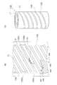
図3には、マイクロ流体デバイス10を斜め上から見た状態が示されている。図3に表れているマイクロ流体デバイス10を構成している部材は、円柱棒状の導体軸11と、導体軸11の周りに巻回されている絶縁性の透明フィルム12と、透明フィルム12を収納している中空円筒状の透明のケース13と、透明フィルム12の下部に取り付けられている剛性の高い樹脂製の漏斗14と、透明フィルム12に形成されている第1電極15及び第2電極16の一部である。後述するように、ケース13は熱収縮する材料で構成されており、例えばポリエチレンテレフタレート(PET)のシュリンクフィルムを用いることができる。
図4に示されているように、第1電極15及び第2電極16は、透明フィルム12の表面側に形成されており、第1電極15も第2電極16も透明の導電材料で構成されている。マイクロ流体デバイス10は、図4及び図5に示されているように、透明フィルム12の裏面側に形成されている接地電極17及びスペーサ18をさらに備えている。接地電極17も、第1電極15や第2電極16と同様に、光透過性と屈曲性を有する導電材料で形成されている。
図3には、マイクロ流体デバイス10を斜め上から見た状態が示されている。図3に表れているマイクロ流体デバイス10を構成している部材は、円柱棒状の導体軸11と、導体軸11の周りに巻回されている絶縁性の透明フィルム12と、透明フィルム12を収納している中空円筒状の透明のケース13と、透明フィルム12の下部に取り付けられている剛性の高い樹脂製の漏斗14と、透明フィルム12に形成されている第1電極15及び第2電極16の一部である。後述するように、ケース13は熱収縮する材料で構成されており、例えばポリエチレンテレフタレート(PET)のシュリンクフィルムを用いることができる。
図4に示されているように、第1電極15及び第2電極16は、透明フィルム12の表面側に形成されており、第1電極15も第2電極16も透明の導電材料で構成されている。マイクロ流体デバイス10は、図4及び図5に示されているように、透明フィルム12の裏面側に形成されている接地電極17及びスペーサ18をさらに備えている。接地電極17も、第1電極15や第2電極16と同様に、光透過性と屈曲性を有する導電材料で形成されている。
(3-1)透明フィルム
透明フィルム12は、PET、ポリメタクリル酸メチル(PMMA)、ポリカーボネート(PC)及びポリウレタンなどの透明な樹脂からなる。これらの樹脂は、高い絶縁性を有している。透明フィルム12の厚みは、巻回して流路を形成することを考慮すると、50μm~500μm程度が好ましい。なお、第1実施形態においては、検出部50で光学的な検出を行うため透明フィルム12が使用されるが、光を用いない方法で検出を行う場合や検出部50を設けないような誘電泳動装置の場合には不透明な絶縁シートを用いることもできる。
透明フィルム12には、第1電極15と第2電極16をそれぞれ外部の配線に接続するための電極取り出し部12a,12bが設けられている。この電極取り出し部12a,12bにそれぞれ形成されている引き出し部15b,16bが形成されている。図4の矢印AW1の方向が流体の流れる方向、つまり流路の向きである。この電極取り出し部12a,12bは、流体が流れる方向に長く延びているので、透明フィルム12を円筒に巻いたときに円筒の上端部よりも外に突出すように構成できる。
透明フィルム12は、PET、ポリメタクリル酸メチル(PMMA)、ポリカーボネート(PC)及びポリウレタンなどの透明な樹脂からなる。これらの樹脂は、高い絶縁性を有している。透明フィルム12の厚みは、巻回して流路を形成することを考慮すると、50μm~500μm程度が好ましい。なお、第1実施形態においては、検出部50で光学的な検出を行うため透明フィルム12が使用されるが、光を用いない方法で検出を行う場合や検出部50を設けないような誘電泳動装置の場合には不透明な絶縁シートを用いることもできる。
透明フィルム12には、第1電極15と第2電極16をそれぞれ外部の配線に接続するための電極取り出し部12a,12bが設けられている。この電極取り出し部12a,12bにそれぞれ形成されている引き出し部15b,16bが形成されている。図4の矢印AW1の方向が流体の流れる方向、つまり流路の向きである。この電極取り出し部12a,12bは、流体が流れる方向に長く延びているので、透明フィルム12を円筒に巻いたときに円筒の上端部よりも外に突出すように構成できる。
(3-2)電極
第1電極15、第2電極16及び接地電極17は、透明フィルム12と同様の理由から第1実施形態においては、光透過性と屈曲性を有するカーボンナノチューブ(CNT)、ポリ3,4-エチレンジオキシチオフェン(PEDOT)、金属ナノファイバ、金属メッシュ及び薄膜めっきなどで形成されている。ここでいう金属とは、例えば銅(Cu)、銀(Ag)、アルミニウム(Al)及び金(Au)などである。
第1電極15と第2電極16は、図4に示されているように、櫛歯15a,16aが交互に並ぶように配置されている一対の櫛型電極である。図4に示されている第1電極15と第2電極16の櫛歯15a,16aは、流路に対して直交する向きに延びている。つまり、流体の流れる方向である矢印AW1に対して櫛歯15a,16aが直交するように配置されている。
接地電極17の形成されている透明フィルム12の裏面側が、透明フィルム12を巻回しするときに内側に巻き込まれる。つまり、一対の第1電極15と第2電極16の形成されている表面側が円筒の外側に表れる。
第1電極15、第2電極16及び接地電極17は、透明フィルム12と同様の理由から第1実施形態においては、光透過性と屈曲性を有するカーボンナノチューブ(CNT)、ポリ3,4-エチレンジオキシチオフェン(PEDOT)、金属ナノファイバ、金属メッシュ及び薄膜めっきなどで形成されている。ここでいう金属とは、例えば銅(Cu)、銀(Ag)、アルミニウム(Al)及び金(Au)などである。
第1電極15と第2電極16は、図4に示されているように、櫛歯15a,16aが交互に並ぶように配置されている一対の櫛型電極である。図4に示されている第1電極15と第2電極16の櫛歯15a,16aは、流路に対して直交する向きに延びている。つまり、流体の流れる方向である矢印AW1に対して櫛歯15a,16aが直交するように配置されている。
接地電極17の形成されている透明フィルム12の裏面側が、透明フィルム12を巻回しするときに内側に巻き込まれる。つまり、一対の第1電極15と第2電極16の形成されている表面側が円筒の外側に表れる。
(3-3)スペーサ
スペーサ18は、絶縁体である。スペーサ18は、例えば円柱、球、ドーム、四角柱などの形状に設計される。スペーサ18の高さは、例えば100μm~500μmに設定されるのが好ましい。このスペーサ18の配置は、例えば、図6に示されているような千鳥配置にすることができる。千鳥配置にするときの横方向のピッチPcと縦方向のピッチPlは、例えば0.5mm~3mmの範囲内で設定されるのが好ましい。スペーサ18の材料には、PET、PMMA、PC、アクリロニトリルブタジエンスチレン(ABS)、ポリジメチルシロキサン(PDMS)、ポリイミド(PI)、ポリエーテルエーテルケトン(PEEK)及びレジストなどが用いられる。スペーサ18は、透明であってもよく、不透明であってもよい。
スペーサ18は、絶縁体である。スペーサ18は、例えば円柱、球、ドーム、四角柱などの形状に設計される。スペーサ18の高さは、例えば100μm~500μmに設定されるのが好ましい。このスペーサ18の配置は、例えば、図6に示されているような千鳥配置にすることができる。千鳥配置にするときの横方向のピッチPcと縦方向のピッチPlは、例えば0.5mm~3mmの範囲内で設定されるのが好ましい。スペーサ18の材料には、PET、PMMA、PC、アクリロニトリルブタジエンスチレン(ABS)、ポリジメチルシロキサン(PDMS)、ポリイミド(PI)、ポリエーテルエーテルケトン(PEEK)及びレジストなどが用いられる。スペーサ18は、透明であってもよく、不透明であってもよい。
(4)マイクロ流体デバイスの製造方法
(4-1)製造工程の概要
マイクロ流体デバイスの製造方法について、図7乃至図11を用いて説明する。図7は、マイクロ流体デバイス10の製造工程の概要を示すフローチャートである。マイクロ流体デバイス10の製造においては、まず、図4及び図5に示されている第1電極15、第2電極16及び接地電極17が形成される電極パターニング工程S1が実施される。電極のパターニングは、両面に金属箔が形成されている、透明フィルム12の材料である長尺の透明フィルム80(図8(a)参照)を用いて連続的に行われる。例えばスクリーン印刷などによってマスキングした後に、金属箔がエッチングされることによって、図4及び図5に示されているような形状に金属箔がパターニングされて、第1電極15、第2電極16及び接地電極17が形成される。
次に、スペーサ配置工程S2が実施される。図5及び図6に示されているスペーサ18は、スペーサフィルムを用いる方法、フォトレジストをパターニングする方法及びドットスペーサを配置する方法などを用いて形成される。これらのうちのスペーサフィルムを用いる方法について後述する。これらの方法も長尺の透明フィルム80に対して連続して行うことができる。
次に、第1電極15、第2電極16及び接地電極17並びにスペーサ18が形成された長尺の透明フィルム80の外形がカットされる(フィルム外形カット工程S3)。このカットによって、平面形状が長方形をした透明フィルム12が形成される。そして、透明フィルム12の一辺に沿って導体軸11が接着される(軸・フィルム接着工程S4)。導体軸11と透明フィルム12の接着が完了した後、例えば接着剤が乾燥した後に、透明フィルム12が導体軸11の周りにスクロール状に巻き付けられる(フィルム巻き付け工程S5)。最後に、導体軸11に巻き付けられた透明フィルム12が円筒状のケース13に組み込まれる(ケース組込み工程S6)。これらフィルム巻き付け工程S5とケース組込み工程S6を含むマイクロ流体デバイスの組み立てについては後ほど説明する。
(4-1)製造工程の概要
マイクロ流体デバイスの製造方法について、図7乃至図11を用いて説明する。図7は、マイクロ流体デバイス10の製造工程の概要を示すフローチャートである。マイクロ流体デバイス10の製造においては、まず、図4及び図5に示されている第1電極15、第2電極16及び接地電極17が形成される電極パターニング工程S1が実施される。電極のパターニングは、両面に金属箔が形成されている、透明フィルム12の材料である長尺の透明フィルム80(図8(a)参照)を用いて連続的に行われる。例えばスクリーン印刷などによってマスキングした後に、金属箔がエッチングされることによって、図4及び図5に示されているような形状に金属箔がパターニングされて、第1電極15、第2電極16及び接地電極17が形成される。
次に、スペーサ配置工程S2が実施される。図5及び図6に示されているスペーサ18は、スペーサフィルムを用いる方法、フォトレジストをパターニングする方法及びドットスペーサを配置する方法などを用いて形成される。これらのうちのスペーサフィルムを用いる方法について後述する。これらの方法も長尺の透明フィルム80に対して連続して行うことができる。
次に、第1電極15、第2電極16及び接地電極17並びにスペーサ18が形成された長尺の透明フィルム80の外形がカットされる(フィルム外形カット工程S3)。このカットによって、平面形状が長方形をした透明フィルム12が形成される。そして、透明フィルム12の一辺に沿って導体軸11が接着される(軸・フィルム接着工程S4)。導体軸11と透明フィルム12の接着が完了した後、例えば接着剤が乾燥した後に、透明フィルム12が導体軸11の周りにスクロール状に巻き付けられる(フィルム巻き付け工程S5)。最後に、導体軸11に巻き付けられた透明フィルム12が円筒状のケース13に組み込まれる(ケース組込み工程S6)。これらフィルム巻き付け工程S5とケース組込み工程S6を含むマイクロ流体デバイスの組み立てについては後ほど説明する。
(4-2)スペーサの形成
図8(a)に示されているのは、第1電極15、第2電極16及び接地電極17の形成された長尺の透明フィルム80に長尺のスペーサフィルム81が貼合された状態である。次に、図8(b)に示されているように、ダイカットロール82によってスペーサ18になる部分とそれ以外の部分を分離できるようにスペーサフィルム81がハーフカットされる。長尺のスペーサフィルム81の不要な部分81aが除去されて、スペーサ18が長尺の透明フィルム80に残る(図8(c)参照)。このように不要な部分81aが除去された長尺の透明フィルム80はロール状に巻き取られて保管される。そして、マイクロ流体デバイス10の製造時に、必要な枚数の透明フィルム12が長尺の透明フィルム80から切り出される。
図8(a)に示されているのは、第1電極15、第2電極16及び接地電極17の形成された長尺の透明フィルム80に長尺のスペーサフィルム81が貼合された状態である。次に、図8(b)に示されているように、ダイカットロール82によってスペーサ18になる部分とそれ以外の部分を分離できるようにスペーサフィルム81がハーフカットされる。長尺のスペーサフィルム81の不要な部分81aが除去されて、スペーサ18が長尺の透明フィルム80に残る(図8(c)参照)。このように不要な部分81aが除去された長尺の透明フィルム80はロール状に巻き取られて保管される。そして、マイクロ流体デバイス10の製造時に、必要な枚数の透明フィルム12が長尺の透明フィルム80から切り出される。
(4-3)マイクロ流体デバイスの組み立て
図9(a)乃至図9(e)には、マイクロ流体デバイス10の組立工程が示されている。導体軸11に巻き付けられた円筒状の透明フィルム12は、まず、図9(a)に示されているように、その下方の端部が漏斗14に嵌め込まれる。次に、図9(b)に示されている円筒状のガイド85が導体軸11の上方の端部に嵌め込まれる。この円筒状のガイド85の外径は、円筒状の透明フィルム12の外径と同じか、又は透明フィルム12の外径よりも少し大きく設定されている。ただし、ガイド85の外径は、漏斗14の外径と同じか、又は漏斗14の外径よりも小さく設定されている。このガイド85の外側を通って中空円筒状のケース13が漏斗14の外周に嵌め込まれる(図9(c)参照)。このようにケース13が漏斗14に嵌るように、ケース13の内径は、漏斗14の外径よりも大きく設定されている。ケース13が熱で収縮する材料で形成されていることから、図9(c)の状態で全体を加熱することによりケース13が収縮して、図9(d)に示されている状態になる。図9(d)の状態になるように加熱を停止させるため、例えばケース13の外径がガイド85の外径に一致したところを基準として加熱停止のタイミングがはかられる。加熱が停止されてケース13の収縮が止まったら、ガイド85が導体軸11から外されてマイクロ流体デバイス10の組み立てが完了する(図9(e)参照)。ケース13が熱収縮してケース13の内壁が透明フィルム12の最外周に密着し、かつケース13の内壁が漏斗14の外周で固定されることにより、円筒状に巻かれた透明フィルム12の外側が支持されて漏斗14と透明フィルム12は固定される。
図9(a)乃至図9(e)には、マイクロ流体デバイス10の組立工程が示されている。導体軸11に巻き付けられた円筒状の透明フィルム12は、まず、図9(a)に示されているように、その下方の端部が漏斗14に嵌め込まれる。次に、図9(b)に示されている円筒状のガイド85が導体軸11の上方の端部に嵌め込まれる。この円筒状のガイド85の外径は、円筒状の透明フィルム12の外径と同じか、又は透明フィルム12の外径よりも少し大きく設定されている。ただし、ガイド85の外径は、漏斗14の外径と同じか、又は漏斗14の外径よりも小さく設定されている。このガイド85の外側を通って中空円筒状のケース13が漏斗14の外周に嵌め込まれる(図9(c)参照)。このようにケース13が漏斗14に嵌るように、ケース13の内径は、漏斗14の外径よりも大きく設定されている。ケース13が熱で収縮する材料で形成されていることから、図9(c)の状態で全体を加熱することによりケース13が収縮して、図9(d)に示されている状態になる。図9(d)の状態になるように加熱を停止させるため、例えばケース13の外径がガイド85の外径に一致したところを基準として加熱停止のタイミングがはかられる。加熱が停止されてケース13の収縮が止まったら、ガイド85が導体軸11から外されてマイクロ流体デバイス10の組み立てが完了する(図9(e)参照)。ケース13が熱収縮してケース13の内壁が透明フィルム12の最外周に密着し、かつケース13の内壁が漏斗14の外周で固定されることにより、円筒状に巻かれた透明フィルム12の外側が支持されて漏斗14と透明フィルム12は固定される。
(4-4)透明フィルム12の巻き始めと巻き終わり
まず、巻き始め(軸心側)の透明フィルム12の構造について説明する。図10において、導体軸11は例えば導電性接着剤が塗られた接地電極17の上に置かれる。そして、導体軸11は、矢印AW2の方向に一周だけ接地電極17に巻き付けられる。従って、透明フィルム12の軸心側の接着領域Ar1は、導体軸11の外周と同じ長さを有している。図10からも分かるように、この接着領域Ar1には、導体軸11と接地電極17との電気的な接続を行わせるため、スペーサ18は配置されていない。
ところで、透明フィルム12を導体軸11の周りに巻き付けると、巻き始めと巻き終わりを除き、スペーサ18によって任意の周とその外側の周との間に、一定の間隔の隙間が形成される。そして、この隙間が流路2になる。流路2は、導体軸11が延びる中心軸方向に向かって延びている。この流路2によって、導体軸11の長手方向に対して垂直な断面(中心軸に対して垂直な断面)において透明フィルム12が渦巻状になる(図12参照)。つまり、流路2も渦巻状の断面形状を持つことになる。
図12は、図11のI-I線に沿って切断した断面図である。図11と図12を参照すると、巻き始めと巻き終わりに断面形状が楔形をした透明のスペーサ19a,19bが挿入されているのが分かる。例えば、導体軸11の周りに透明フィルム12が巻き付けられるときに、これら楔形のスペーサ19a,19bを一緒に巻き込む。それにより、図12の流路領域Ar2に流体が流れる。このようなスペーサ19a,19bによって巻き始めと巻き終わりの隙間の間隔が一定でないところに流体が流れなくなるということは、言い換えると、流路の高さが一定になるということである。流路の高さが一定になると、誘電泳動によって均一な粒子の分離が行えるので、粒子の分析や粒子の分留の精度が向上する。このような誘電泳動としては、例えば数種類の粒子が混在している懸濁液の中から粒子の誘電率の違いを利用して分離する誘電泳動がある。
まず、巻き始め(軸心側)の透明フィルム12の構造について説明する。図10において、導体軸11は例えば導電性接着剤が塗られた接地電極17の上に置かれる。そして、導体軸11は、矢印AW2の方向に一周だけ接地電極17に巻き付けられる。従って、透明フィルム12の軸心側の接着領域Ar1は、導体軸11の外周と同じ長さを有している。図10からも分かるように、この接着領域Ar1には、導体軸11と接地電極17との電気的な接続を行わせるため、スペーサ18は配置されていない。
ところで、透明フィルム12を導体軸11の周りに巻き付けると、巻き始めと巻き終わりを除き、スペーサ18によって任意の周とその外側の周との間に、一定の間隔の隙間が形成される。そして、この隙間が流路2になる。流路2は、導体軸11が延びる中心軸方向に向かって延びている。この流路2によって、導体軸11の長手方向に対して垂直な断面(中心軸に対して垂直な断面)において透明フィルム12が渦巻状になる(図12参照)。つまり、流路2も渦巻状の断面形状を持つことになる。
図12は、図11のI-I線に沿って切断した断面図である。図11と図12を参照すると、巻き始めと巻き終わりに断面形状が楔形をした透明のスペーサ19a,19bが挿入されているのが分かる。例えば、導体軸11の周りに透明フィルム12が巻き付けられるときに、これら楔形のスペーサ19a,19bを一緒に巻き込む。それにより、図12の流路領域Ar2に流体が流れる。このようなスペーサ19a,19bによって巻き始めと巻き終わりの隙間の間隔が一定でないところに流体が流れなくなるということは、言い換えると、流路の高さが一定になるということである。流路の高さが一定になると、誘電泳動によって均一な粒子の分離が行えるので、粒子の分析や粒子の分留の精度が向上する。このような誘電泳動としては、例えば数種類の粒子が混在している懸濁液の中から粒子の誘電率の違いを利用して分離する誘電泳動がある。
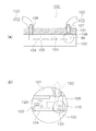
また、巻き始めと巻き終わりには、図4に示されている電極取り出し分12a,12bが配置される。図13(a)は、図12に示されているマイクロ流体デバイス10の一部領域ABを模式的に示す拡大断面図であり、図13(b)はマイクロ流体デバイス10の他の領域ACを模式的に示す拡大断面図である。電源部40の高周波電源41は、一方の電源端子41aが引き出し部15bに接続され、他方の電源端子41bが引き出し部16bに接続される。また、導体軸11には電源部40の接地端子42が接続される。
高周波電源41から第1電極15と第2電極16との間に高周波電圧を印加すると、図14に示されているように、異なる2種類の粒子3a,3bのうち、一方の粒子3aが第1電極15と第2電極16との間にトラップされ、他方の粒子3bがトラップされずに流路2を流れる。なお、図14において、第1電極15と第2電極16との間に描かれている曲線は電界を表しており、矢印AW3が流体の流れる向きを表している。この状態で光ファイバ52a(図2参照)から光が照射されると、トラップされている粒子3aの特性に応じた周波数の光の吸収や反射などが生じる。従って、図2に示されている検出デバイス51を使って、光ファイバ52aで受光した光を分光器51aで分光してフィッティング処理デバイス51bで処理することで、モニタ出力デバイス51cに粒子3aのトラップに関する表示を行うことができる。
高周波電源41から第1電極15と第2電極16との間に高周波電圧を印加すると、図14に示されているように、異なる2種類の粒子3a,3bのうち、一方の粒子3aが第1電極15と第2電極16との間にトラップされ、他方の粒子3bがトラップされずに流路2を流れる。なお、図14において、第1電極15と第2電極16との間に描かれている曲線は電界を表しており、矢印AW3が流体の流れる向きを表している。この状態で光ファイバ52a(図2参照)から光が照射されると、トラップされている粒子3aの特性に応じた周波数の光の吸収や反射などが生じる。従って、図2に示されている検出デバイス51を使って、光ファイバ52aで受光した光を分光器51aで分光してフィッティング処理デバイス51bで処理することで、モニタ出力デバイス51cに粒子3aのトラップに関する表示を行うことができる。
<第2実施形態>
本発明の第2実施形態に係るマイクロ流体デバイス及び誘電泳動装置は、電極の形態を除いては第1実施形態のマイクロ流体デバイス10及び誘電泳動装置1と同じである。第1実施形態のマイクロ流体デバイス10が第1電極15と第2電極の2つの櫛型電極を有しているのに対し、第2実施形態のマイクロ流体デバイスは一つの櫛型電極しか有していない点が異なっている。そのため、以下においては、第2実施形態のマイクロ流体デバイスの透明フィルムと電極について説明し、他の構成については説明を省略する。
本発明の第2実施形態に係るマイクロ流体デバイス及び誘電泳動装置は、電極の形態を除いては第1実施形態のマイクロ流体デバイス10及び誘電泳動装置1と同じである。第1実施形態のマイクロ流体デバイス10が第1電極15と第2電極の2つの櫛型電極を有しているのに対し、第2実施形態のマイクロ流体デバイスは一つの櫛型電極しか有していない点が異なっている。そのため、以下においては、第2実施形態のマイクロ流体デバイスの透明フィルムと電極について説明し、他の構成については説明を省略する。
(5)透明フィルムと電極
図15(a)には、第2実施形態の透明フィルムと電極が模式的に示されている。なお、透明フィルム12Aと櫛型電極15A以外のマイクロ流体デバイス10Aの構成は、マイクロ流体デバイス10と同様であるので、図15(a)では図示省略されている。透明フィルム12Aは、第1実施形態の透明フィルム12と同じ材質で形成され、厚みも同じに構成される。なお、第1実施形態と同様に第2実施形態においても、検出部50で光を用いない方法で検出を行う場合や検出部50を設けないような誘電泳動装置の場合には不透明な絶縁シートを用いることができる。
透明フィルム12Aには、一つの電極取り出し部12Aaが設けられている。これは、一つの櫛型電極15Aのみが透明フィルム12Aの表面側に形成されているためである。透明フィルム12Aの裏面側には、接地電極17Aが形成されている。この透明フィルム12Aは第1実施形態の透明フィルム12と同様にスクロール状に巻回される(図15(b)参照)。そして、櫛型電極15Aは、図15(b)に示されている電源部40Aの高周波電源41の一方の電源端子41aに接続され、接地電極17Aは、高周波電源41の他方の電源端子41bに接続される。ここでは、他方の電源端子41bが接地端子42に接続されている。このような第2実施形態の誘電泳動装置1Aは、この電源部40Aの構成を除いて第1実施形態の誘電泳動装置1と同様に構成できる。そのため、図15(b)では、電源部40Aと導体軸11と透明フィルム12Aと櫛型電極15A以外の誘電泳動装置1Aの構成は、誘電泳動装置1と同様であるので、図示省略されている。
図16には、マイクロ流体デバイス10Aの内部で異種の粒子が分離されている状態が示されている。図16において、矢印AW4が流体の流れる方向である。高周波電界は、櫛型電極15Aと接地電極17Aとの間で生じている。図16に示されている高周波電界では、粒子3cがトラップされ、粒子3dが流路2Aを通過している。この高周波電界の周波数が変化すると、粒子3cのトラップを解除することができる。
図15(a)には、第2実施形態の透明フィルムと電極が模式的に示されている。なお、透明フィルム12Aと櫛型電極15A以外のマイクロ流体デバイス10Aの構成は、マイクロ流体デバイス10と同様であるので、図15(a)では図示省略されている。透明フィルム12Aは、第1実施形態の透明フィルム12と同じ材質で形成され、厚みも同じに構成される。なお、第1実施形態と同様に第2実施形態においても、検出部50で光を用いない方法で検出を行う場合や検出部50を設けないような誘電泳動装置の場合には不透明な絶縁シートを用いることができる。
透明フィルム12Aには、一つの電極取り出し部12Aaが設けられている。これは、一つの櫛型電極15Aのみが透明フィルム12Aの表面側に形成されているためである。透明フィルム12Aの裏面側には、接地電極17Aが形成されている。この透明フィルム12Aは第1実施形態の透明フィルム12と同様にスクロール状に巻回される(図15(b)参照)。そして、櫛型電極15Aは、図15(b)に示されている電源部40Aの高周波電源41の一方の電源端子41aに接続され、接地電極17Aは、高周波電源41の他方の電源端子41bに接続される。ここでは、他方の電源端子41bが接地端子42に接続されている。このような第2実施形態の誘電泳動装置1Aは、この電源部40Aの構成を除いて第1実施形態の誘電泳動装置1と同様に構成できる。そのため、図15(b)では、電源部40Aと導体軸11と透明フィルム12Aと櫛型電極15A以外の誘電泳動装置1Aの構成は、誘電泳動装置1と同様であるので、図示省略されている。
図16には、マイクロ流体デバイス10Aの内部で異種の粒子が分離されている状態が示されている。図16において、矢印AW4が流体の流れる方向である。高周波電界は、櫛型電極15Aと接地電極17Aとの間で生じている。図16に示されている高周波電界では、粒子3cがトラップされ、粒子3dが流路2Aを通過している。この高周波電界の周波数が変化すると、粒子3cのトラップを解除することができる。
(6)特徴
(6-1)
以上説明したように、透明フィルム12,12A(絶縁シートの例)は、中心軸の周りに巻回され、図11などに示されているように、中心軸に垂直な断面における形状が渦巻状である。また、図12などに示されているように、例えば透明フィルム12,12Aの所定の周r1とその外側の周r2との間に配置されて所定の周r1と外側の周r2にある透明フィルム12の間にスペーサ18が配置され、隙間が設けられている。この隙間が流路2,2Aであって、流路2,2Aは、導体軸11に垂直な断面、つまり中心軸に垂直な断面における形状が渦巻状であって中心軸に沿って延びている。円筒状のマイクロ流体デバイス10,10Aのケース13の断面内周のうち薄い透明フィルム12,12Aと導体軸が占める面積以外のほぼ全てが渦巻状の流路2,2Aであり、巻かれた透明フィルム12,12Aの断面に占める渦巻状の流路の占有割合が大きくなるので、大量の粒子を精度よく分離し易くなる。
(6-1)
以上説明したように、透明フィルム12,12A(絶縁シートの例)は、中心軸の周りに巻回され、図11などに示されているように、中心軸に垂直な断面における形状が渦巻状である。また、図12などに示されているように、例えば透明フィルム12,12Aの所定の周r1とその外側の周r2との間に配置されて所定の周r1と外側の周r2にある透明フィルム12の間にスペーサ18が配置され、隙間が設けられている。この隙間が流路2,2Aであって、流路2,2Aは、導体軸11に垂直な断面、つまり中心軸に垂直な断面における形状が渦巻状であって中心軸に沿って延びている。円筒状のマイクロ流体デバイス10,10Aのケース13の断面内周のうち薄い透明フィルム12,12Aと導体軸が占める面積以外のほぼ全てが渦巻状の流路2,2Aであり、巻かれた透明フィルム12,12Aの断面に占める渦巻状の流路の占有割合が大きくなるので、大量の粒子を精度よく分離し易くなる。
マイクロ流体デバイス10,10Aの電極には、透明フィルム12,12Aの表面に形成されている第1電極15及び第2電極16や櫛型電極15A(電圧印加電極の例)並びに透明フィルム12,12Aの裏面に矩形状に形成されている接地電極17がある。この場合、スクロール状に巻回された透明フィルム12,12Aにおいて、図14や図16などに示されているように、隣接する流路2,2Aの第1電極15及び第2電極16の電界を接地電極17でシールドできるなど、適切な位置に接地電極17を配置し易くなる。
上述の説明では、第1電極15及び第2電極16や櫛型電極15Aが流体の流れる方向に対して直交する向きに櫛歯15a,16aが延びる場合について説明した。しかし、図17のマイクロ流体デバイス10Bにおいて、一対の第1電極15B(櫛型電極の例)及び第2電極16B(櫛型電極の例)は、交互に並ぶ櫛歯15Ba,16Baの延びる方向が、流路の延びる方向(矢印AW5の方向)に対して直交する向きよりも傾斜した向きであって直交する方向とのなす角が45度(矢印AW6の方向)までの範囲で設定されている。この場合、第1電極15Bと第2電極16Bの櫛歯15Ba,16Baの間に既にトラップされている粒子3eがあっても、後から流れてくる粒子3fがトラップされている粒子3eを避けて通りやすくなり、大量の粒子を分離するときの精度が向上する。
櫛歯15a,16aが延びる方向についてもう少し詳しく説明する。まず、図17の矢印AW7の方向が流路の延びる方向(矢印AW5の方向)に対して直交する向きである。この矢印AW7の向きよりもθ度だけ傾斜した向きが矢印AW8の方向である。
なお、この矢印AW7の方向とのなす角θが45度よりも大きいと(例えば矢印AW9の向きに櫛歯15a,16aが延びると)、トラップすべき粒子3eが流体の流れによって流されやすくなるので、傾斜する角度θは45度以下が好ましい。つまり、矢印AW6の方向が直交する向きとのなす角が45度の方向であるから、矢印AW6の方向を境界として矢印AW8のある方が好ましい方向で矢印AW9のある方が好ましくない方向である。
また、図15に示されている櫛型電極15Aの場合も、櫛歯15Aaの延びる方向が櫛歯15Ba,16Baと同様に傾斜していてもよい。
櫛歯15a,16aが延びる方向についてもう少し詳しく説明する。まず、図17の矢印AW7の方向が流路の延びる方向(矢印AW5の方向)に対して直交する向きである。この矢印AW7の向きよりもθ度だけ傾斜した向きが矢印AW8の方向である。
なお、この矢印AW7の方向とのなす角θが45度よりも大きいと(例えば矢印AW9の向きに櫛歯15a,16aが延びると)、トラップすべき粒子3eが流体の流れによって流されやすくなるので、傾斜する角度θは45度以下が好ましい。つまり、矢印AW6の方向が直交する向きとのなす角が45度の方向であるから、矢印AW6の方向を境界として矢印AW8のある方が好ましい方向で矢印AW9のある方が好ましくない方向である。
また、図15に示されている櫛型電極15Aの場合も、櫛歯15Aaの延びる方向が櫛歯15Ba,16Baと同様に傾斜していてもよい。
マイクロ流体デバイス10,10Aの導体軸11は、中心軸に沿って透明フィルム12,12Aの最内周に配置され、接地電極17,17Aに電気的に接続されている。そのため、導体軸11を電源部40の接地端子42に接続すれば接地電極17,17Aが接地でき、絶縁性の透明フィルム12,12Aに巻き込まれる接地電極17,17Aの接地が容易になる。
誘電泳動装置1,1Aは、上述のマイクロ流体デバイス10,10Aを備え、そしてマイクロ流体デバイス10,10Aに対して流体を流すための送液ポンプ20(送液装置の例)と、電極に電力を供給するための電源部40とを備えているので、誘電泳動装置1,1Aも大量の粒子を精度よく分離することができる。
(6-2)
中空円筒状のケース13は、図12などに示されているように、透明フィルム12,12Aの最外周に沿う内壁13aを有している。このケース13によって、ケース13の一方の開口部13bから他方の開口部13cに向けて流路2,2Aを通して流体が流れるように構成されている。一方の開口部13bから他方の開口部13cに向けてケース13の中に流体を流すことによって、流路2,2Aに流体を導けるので大量の流体をマイクロ流体デバイス10,10Aに通しやすくなり、大量の粒子の分離が容易になる。
中空円筒状のケース13は、図12などに示されているように、透明フィルム12,12Aの最外周に沿う内壁13aを有している。このケース13によって、ケース13の一方の開口部13bから他方の開口部13cに向けて流路2,2Aを通して流体が流れるように構成されている。一方の開口部13bから他方の開口部13cに向けてケース13の中に流体を流すことによって、流路2,2Aに流体を導けるので大量の流体をマイクロ流体デバイス10,10Aに通しやすくなり、大量の粒子の分離が容易になる。
(6-3)
図3などに示されている漏斗14は、ケース13の他方の開口部13cに取り付けられている。この漏斗14を使って、流路2,2Aを通過した流体が回収される。このように流路2,2Aを通過した流体は、漏斗14によって簡単に回収される。
図3などに示されている漏斗14は、ケース13の他方の開口部13cに取り付けられている。この漏斗14を使って、流路2,2Aを通過した流体が回収される。このように流路2,2Aを通過した流体は、漏斗14によって簡単に回収される。
(6-4)
流路2,2Aは、楔形のスペーサ19a、19bによって巻き始めと巻き終わりの部分に流体が流れないように構成される。つまり、透明フィルム12,12Aの巻き始めと巻き終わりの隙間の間隔が変化する領域を除いた隙間の間隔が一定の領域に形成されている。この場合、流路2,2Aの高さを一定に揃えることができるので、渦巻状の流路2,2Aの高さに起因する流速の差を小さくでき、高い粒子の分離精度を得やすくなる。
流路2,2Aは、楔形のスペーサ19a、19bによって巻き始めと巻き終わりの部分に流体が流れないように構成される。つまり、透明フィルム12,12Aの巻き始めと巻き終わりの隙間の間隔が変化する領域を除いた隙間の間隔が一定の領域に形成されている。この場合、流路2,2Aの高さを一定に揃えることができるので、渦巻状の流路2,2Aの高さに起因する流速の差を小さくでき、高い粒子の分離精度を得やすくなる。
(7)変形例
(7-1)
上記第1実施形態及び第2実施形態では、流路2は中心軸に対する垂直な断面において渦巻状に繋がった形状の場合について説明した。つまり、所定の周とその外周にある透明フィルム12,12Aの隙間が島状に点在するスペーサ18によって形成されて流路2が形成されている。そのため、断面渦巻状の流路2は、渦巻きの方向に流体が移動できるものとなっている。しかし、渦巻きに沿う方向への流体の流れを、例えば中心軸に沿って伸びるリブなどによって制限し、中心軸方向に沿う流体の流れを整えるように構成することもできる。
(7-1)
上記第1実施形態及び第2実施形態では、流路2は中心軸に対する垂直な断面において渦巻状に繋がった形状の場合について説明した。つまり、所定の周とその外周にある透明フィルム12,12Aの隙間が島状に点在するスペーサ18によって形成されて流路2が形成されている。そのため、断面渦巻状の流路2は、渦巻きの方向に流体が移動できるものとなっている。しかし、渦巻きに沿う方向への流体の流れを、例えば中心軸に沿って伸びるリブなどによって制限し、中心軸方向に沿う流体の流れを整えるように構成することもできる。
(7-2)
上記第1実施形態及び第2実施形態では、一枚の透明フィルム12,12Aの表面側と裏面側とを用いて流路2が構成されている。このように、一枚の透明フィルム12,12Aで構成する方が、材料が少なくて済むという点で好ましい。しかし、例えば、2枚の絶縁シートをそれぞれ表面側と裏面側に別々に配して、それらをスクロール状に巻いて断面渦巻状の流路を構成してもよく、流路を構成するための絶縁シートは一枚の場合に限られない。
上記第1実施形態及び第2実施形態では、一枚の透明フィルム12,12Aの表面側と裏面側とを用いて流路2が構成されている。このように、一枚の透明フィルム12,12Aで構成する方が、材料が少なくて済むという点で好ましい。しかし、例えば、2枚の絶縁シートをそれぞれ表面側と裏面側に別々に配して、それらをスクロール状に巻いて断面渦巻状の流路を構成してもよく、流路を構成するための絶縁シートは一枚の場合に限られない。
(7-3)
上記第1実施形態及び第2実施形態では、透明フィルム12,12Aの巻き始めや巻き終わりに、透明の楔形のスペーサ19a,19bを挿入する場合について説明したが、スペーサ19a,19bが挿入されている領域に流体を流さない構成はこれだけには限られない。例えば、この部分を遮蔽するような壁を設けて、巻き始めと巻き終わりの隙間の間隔が変化する領域を、流路2から分離された中空のスペースとすることもできる。例えば中空のスペースを形成するための壁が透明であれば、検出用の光を透過させることもできる。
上記第1実施形態及び第2実施形態では、透明フィルム12,12Aの巻き始めや巻き終わりに、透明の楔形のスペーサ19a,19bを挿入する場合について説明したが、スペーサ19a,19bが挿入されている領域に流体を流さない構成はこれだけには限られない。例えば、この部分を遮蔽するような壁を設けて、巻き始めと巻き終わりの隙間の間隔が変化する領域を、流路2から分離された中空のスペースとすることもできる。例えば中空のスペースを形成するための壁が透明であれば、検出用の光を透過させることもできる。
(7-4)
上記第1実施形態及び第2実施形態では、ケース13が円筒状で、透明フィルム12,12Aの最外周が円筒状である場合について説明したが、ケース13の内壁13aや透明フィルム12,12Aの最外周の断面形状は円には限られない。例えば、正方形や正方形以外の多角形などであってもよい。
上記第1実施形態及び第2実施形態では、ケース13が円筒状で、透明フィルム12,12Aの最外周が円筒状である場合について説明したが、ケース13の内壁13aや透明フィルム12,12Aの最外周の断面形状は円には限られない。例えば、正方形や正方形以外の多角形などであってもよい。
(7-5)
上記第1実施形態及び第2実施形態では、検出部50を備える誘電泳動装置1,1Aについて説明したが、検出部を設けないで、本願発明の誘電泳動装置を単に分留装置として用いることもできる。
以上、本発明の第1実施形態及び第2実施形態について説明したが、本発明は上記実施形態に限定されるものではなく、発明の要旨を逸脱しない範囲で種々の変更が可能である。特に、本明細書に書かれた複数の実施形態及び変形例は必要に応じて任意に組み合せ可能である。
上記第1実施形態及び第2実施形態では、検出部50を備える誘電泳動装置1,1Aについて説明したが、検出部を設けないで、本願発明の誘電泳動装置を単に分留装置として用いることもできる。
以上、本発明の第1実施形態及び第2実施形態について説明したが、本発明は上記実施形態に限定されるものではなく、発明の要旨を逸脱しない範囲で種々の変更が可能である。特に、本明細書に書かれた複数の実施形態及び変形例は必要に応じて任意に組み合せ可能である。
1,1A 誘電泳動装置
2,2A 流路
10,10A,10B マイクロ流体デバイス
12,12A 透明フィルム
13 ケース
14 漏斗
15,15B 第1電極
15A 櫛型電極
16,16B 第2電極
17 接地電極
18 スペーサ
20 送液ポンプ
30 サンプル回収部
40 電源部
50 検出部
2,2A 流路
10,10A,10B マイクロ流体デバイス
12,12A 透明フィルム
13 ケース
14 漏斗
15,15B 第1電極
15A 櫛型電極
16,16B 第2電極
17 接地電極
18 スペーサ
20 送液ポンプ
30 サンプル回収部
40 電源部
50 検出部
Claims (9)
- 中心軸の周りに巻回され、前記中心軸に垂直な断面における形状の少なくとも一部が渦巻状である絶縁シートと、
前記絶縁シートの所定の周とその外側の周との間に配置されて前記所定の周と前記外側の周にある前記絶縁シートの間に隙間を設け、前記中心軸に垂直な断面における形状の少なくとも一部が渦巻状であって前記中心軸に沿って延び、両端が前記中心軸の軸方向に開口する流路を形成するスペーサと、
前記絶縁シート上に形成され、前記流路を流れる流体内で誘電泳動を生じさせる電界を形成するための電極と、
を備える、マイクロ流体デバイス。 - 前記絶縁シートの最外周に沿う内壁を有し、一方の開口部から他方の開口部に向けて渦巻状の前記流路を通して前記流体を流すための中空筒状のケースをさらに備える、
請求項1に記載のマイクロ流体デバイス。 - 前記ケースの前記他方の開口部に取り付けられ、前記流路を通過した前記流体を回収するための漏斗をさらに備える、
請求項2に記載のマイクロ流体デバイス。 - 前記電極は、前記絶縁シートの表面に形成されている電圧印加電極と、前記絶縁シートの裏面に矩形状に形成されている接地電極とを含む、
請求項1から3のいずれか一項に記載のマイクロ流体デバイス。 - 前記電圧印加電極は、複数の櫛歯を有する櫛型電極である、
請求項4に記載のマイクロ流体デバイス。 - 前記櫛型電極は、複数の前記櫛歯の延びる方向が、前記流路の延びる方向に対して直交する向きよりも傾斜した向きであって直交する向きとのなす角が45度までの範囲で設定されている、
請求項5に記載のマイクロ流体デバイス。 - 前記中心軸に沿って前記絶縁シートの最内周に配置され、前記接地電極に電気的に接続されている棒状の導体軸をさらに備える、
請求項4から6のいずれか一項に記載のマイクロ流体デバイス。 - 前記流路は、前記絶縁シートの巻き始めと巻き終わりの前記隙間の間隔が変化する領域を除いた前記隙間の間隔が一定の領域に形成されている、
請求項1から7のいずれか一項に記載のマイクロ流体デバイス。 - 請求項1から8のいずれかに記載の前記マイクロ流体デバイスと、
前記マイクロ流体デバイスに対して流体を流すための送液装置と、
前記電極に電力を供給するための電源部と、
を備える、誘電泳動装置。
Applications Claiming Priority (2)
| Application Number | Priority Date | Filing Date | Title |
|---|---|---|---|
| JP2013124624A JP5628971B1 (ja) | 2013-06-13 | 2013-06-13 | マイクロ流体デバイス及び誘電泳動装置 |
| JP2013-124624 | 2013-06-13 |
Publications (1)
| Publication Number | Publication Date |
|---|---|
| WO2014199889A1 true WO2014199889A1 (ja) | 2014-12-18 |
Family
ID=52022185
Family Applications (1)
| Application Number | Title | Priority Date | Filing Date |
|---|---|---|---|
| PCT/JP2014/064919 Ceased WO2014199889A1 (ja) | 2013-06-13 | 2014-06-05 | マイクロ流体デバイス及び誘電泳動装置 |
Country Status (3)
| Country | Link |
|---|---|
| JP (1) | JP5628971B1 (ja) |
| TW (1) | TW201502516A (ja) |
| WO (1) | WO2014199889A1 (ja) |
Cited By (3)
| Publication number | Priority date | Publication date | Assignee | Title |
|---|---|---|---|---|
| CN106475160A (zh) * | 2016-11-14 | 2017-03-08 | 哈尔滨工业大学 | 一种基于行波介电泳的细胞与颗粒分离芯片及其制备方法与应用 |
| CN108993341A (zh) * | 2018-08-23 | 2018-12-14 | 浙江工业大学上虞研究院有限公司 | 一种微反应器 |
| WO2020007703A1 (de) * | 2018-07-04 | 2020-01-09 | Robert Bosch Gmbh | Vorrichtung zum dielektrophoretischen einfang von teilchen |
Families Citing this family (2)
| Publication number | Priority date | Publication date | Assignee | Title |
|---|---|---|---|---|
| TWI618968B (zh) * | 2016-12-05 | 2018-03-21 | 達意科技股份有限公司 | 電泳式顯示面板 |
| CN108153078A (zh) | 2016-12-05 | 2018-06-12 | 达意科技股份有限公司 | 电泳式显示面板 |
Citations (9)
| Publication number | Priority date | Publication date | Assignee | Title |
|---|---|---|---|---|
| JPS6463066A (en) * | 1987-09-01 | 1989-03-09 | Nippon Denso Co | Electrostatic oil cleaner |
| JPH06509745A (ja) * | 1991-08-19 | 1994-11-02 | フラウンホッファー−ゲゼルシャフト ツァ フェルダールング デァ アンゲヴァンテン フォアシュンク エー.ファオ. | 微小誘電粒子混合物の連続分離方法およびその方法を実施するための装置 |
| JP2001502226A (ja) * | 1996-09-12 | 2001-02-20 | サイエンティフィック ジェネリクス リミテッド | 分析/分離の方法 |
| JP2004087366A (ja) * | 2002-08-28 | 2004-03-18 | Shinko Electric Ind Co Ltd | 燃料電池セル |
| JP2005310583A (ja) * | 2004-04-22 | 2005-11-04 | Seiko Epson Corp | 燃料電池およびその製造方法 |
| JP2007504952A (ja) * | 2003-05-13 | 2007-03-08 | オーラ バイオシステムズ インコーポレイテッド | 誘電泳動装置 |
| JP2008249513A (ja) * | 2007-03-30 | 2008-10-16 | Kurita Water Ind Ltd | 液中の微粒子数の測定方法及び装置 |
| JP2009214044A (ja) * | 2008-03-11 | 2009-09-24 | Canon Inc | 懸濁液中の粒子の分離方法及び装置 |
| JP2012161727A (ja) * | 2011-02-04 | 2012-08-30 | Nano Cube Japan Co Ltd | マイクロリアクター、マイクロリアクターを用いた触媒反応およびマイクロリアクターを用いた方法 |
Family Cites Families (2)
| Publication number | Priority date | Publication date | Assignee | Title |
|---|---|---|---|---|
| JP2004243455A (ja) * | 2003-02-13 | 2004-09-02 | Pentax Corp | ラボオンアチップおよびその製造方法 |
| US20100062414A1 (en) * | 2007-04-05 | 2010-03-11 | Panasonic Corporation | Sample liquid analytical chip |
-
2013
- 2013-06-13 JP JP2013124624A patent/JP5628971B1/ja not_active Expired - Fee Related
-
2014
- 2014-06-05 WO PCT/JP2014/064919 patent/WO2014199889A1/ja not_active Ceased
- 2014-06-12 TW TW103120278A patent/TW201502516A/zh unknown
Patent Citations (9)
| Publication number | Priority date | Publication date | Assignee | Title |
|---|---|---|---|---|
| JPS6463066A (en) * | 1987-09-01 | 1989-03-09 | Nippon Denso Co | Electrostatic oil cleaner |
| JPH06509745A (ja) * | 1991-08-19 | 1994-11-02 | フラウンホッファー−ゲゼルシャフト ツァ フェルダールング デァ アンゲヴァンテン フォアシュンク エー.ファオ. | 微小誘電粒子混合物の連続分離方法およびその方法を実施するための装置 |
| JP2001502226A (ja) * | 1996-09-12 | 2001-02-20 | サイエンティフィック ジェネリクス リミテッド | 分析/分離の方法 |
| JP2004087366A (ja) * | 2002-08-28 | 2004-03-18 | Shinko Electric Ind Co Ltd | 燃料電池セル |
| JP2007504952A (ja) * | 2003-05-13 | 2007-03-08 | オーラ バイオシステムズ インコーポレイテッド | 誘電泳動装置 |
| JP2005310583A (ja) * | 2004-04-22 | 2005-11-04 | Seiko Epson Corp | 燃料電池およびその製造方法 |
| JP2008249513A (ja) * | 2007-03-30 | 2008-10-16 | Kurita Water Ind Ltd | 液中の微粒子数の測定方法及び装置 |
| JP2009214044A (ja) * | 2008-03-11 | 2009-09-24 | Canon Inc | 懸濁液中の粒子の分離方法及び装置 |
| JP2012161727A (ja) * | 2011-02-04 | 2012-08-30 | Nano Cube Japan Co Ltd | マイクロリアクター、マイクロリアクターを用いた触媒反応およびマイクロリアクターを用いた方法 |
Cited By (5)
| Publication number | Priority date | Publication date | Assignee | Title |
|---|---|---|---|---|
| CN106475160A (zh) * | 2016-11-14 | 2017-03-08 | 哈尔滨工业大学 | 一种基于行波介电泳的细胞与颗粒分离芯片及其制备方法与应用 |
| CN106475160B (zh) * | 2016-11-14 | 2018-10-09 | 哈尔滨工业大学 | 一种基于行波介电泳的细胞与颗粒分离芯片及其制备方法与应用 |
| WO2020007703A1 (de) * | 2018-07-04 | 2020-01-09 | Robert Bosch Gmbh | Vorrichtung zum dielektrophoretischen einfang von teilchen |
| US11975340B2 (en) | 2018-07-04 | 2024-05-07 | Robert Bosch Gmbh | Device for dielectrophoretic capture of particles |
| CN108993341A (zh) * | 2018-08-23 | 2018-12-14 | 浙江工业大学上虞研究院有限公司 | 一种微反应器 |
Also Published As
| Publication number | Publication date |
|---|---|
| JP2015000355A (ja) | 2015-01-05 |
| TW201502516A (zh) | 2015-01-16 |
| JP5628971B1 (ja) | 2014-11-19 |
Similar Documents
| Publication | Publication Date | Title |
|---|---|---|
| JP5628971B1 (ja) | マイクロ流体デバイス及び誘電泳動装置 | |
| Luo et al. | A simplified sheathless cell separation approach using combined gravitational-sedimentation-based prefocusing and dielectrophoretic separation | |
| EP3641934B1 (en) | Microdroplet manipulation device | |
| CN103170384B (zh) | 一种基于大小液滴操控的数字微流芯片 | |
| US8137523B2 (en) | Apparatus for and method of separating polarizable analyte using dielectrophoresis | |
| JP5904958B2 (ja) | 半導体マイクロ分析チップ及びその製造方法 | |
| Yan et al. | An integrated dielectrophoresis-active hydrophoretic microchip for continuous particle filtration and separation | |
| JP2011516884A (ja) | マイクロ流体センサの製造方法 | |
| WO2008020593A1 (en) | Column for chromatography and method for producing the same | |
| US8197656B2 (en) | Device for separating micro particles and a method for fabricating the device | |
| Samiei et al. | Systematic analysis of geometrical based unequal droplet splitting in digital microfluidics | |
| CN103323502B (zh) | 用于流式检测的微流控芯片检测系统 | |
| CN119500300B (zh) | 一种微流控芯片 | |
| JP2011514528A (ja) | デジタルマイクロ流体デバイスとのインターフェース | |
| Dalili et al. | Parametric study on the geometrical parameters of a lab-on-a-chip platform with tilted planar electrodes for continuous dielectrophoretic manipulation of microparticles | |
| CN107335490A (zh) | 一种基于液‑液电润湿效应的可编程控制的微流控芯片 | |
| JP2013529287A (ja) | 駆動電極のアレイを有するマイクロ流体チャネルデバイス | |
| JP2022516386A (ja) | 二相性プラズマ・マイクロリアクタとその使用方法 | |
| EP1337342B1 (de) | Mikrosystem zur dielektrischen und optischen manipulierung von partikeln | |
| CN103406162A (zh) | 基于介质电润湿数字微流芯片的精准液滴产生方法 | |
| Gorbatsova et al. | Electrowetting-on-dielectric actuation of droplets with capillary electrophoretic zones for off-line mass spectrometric analysis | |
| CN103033556A (zh) | 用于微流控芯片上样品直接电喷雾电离的装置及质谱分析方法 | |
| DE19860118C1 (de) | Elektrodenanordnungen zur Erzeugung funktioneller Feldbarrieren in Mikrosystemen | |
| JP2005043345A (ja) | 毛管充填診断センサのセンサフォーマット及び構成方法 | |
| Hoettges et al. | Continuous flow nanoparticle concentration using alternating current‐electroosmotic flow |
Legal Events
| Date | Code | Title | Description |
|---|---|---|---|
| 121 | Ep: the epo has been informed by wipo that ep was designated in this application |
Ref document number: 14810508 Country of ref document: EP Kind code of ref document: A1 |
|
| NENP | Non-entry into the national phase |
Ref country code: DE |
|
| 122 | Ep: pct application non-entry in european phase |
Ref document number: 14810508 Country of ref document: EP Kind code of ref document: A1 |