WO2014185652A1 - 쓰기 트래픽이 적은 캐시 메모리 블록 교체 방법 및 이를 이용한 캐시 서브시스템을 가지는 정보 처리 장치 - Google Patents
쓰기 트래픽이 적은 캐시 메모리 블록 교체 방법 및 이를 이용한 캐시 서브시스템을 가지는 정보 처리 장치 Download PDFInfo
- Publication number
- WO2014185652A1 WO2014185652A1 PCT/KR2014/003996 KR2014003996W WO2014185652A1 WO 2014185652 A1 WO2014185652 A1 WO 2014185652A1 KR 2014003996 W KR2014003996 W KR 2014003996W WO 2014185652 A1 WO2014185652 A1 WO 2014185652A1
- Authority
- WO
- WIPO (PCT)
- Prior art keywords
- cache
- block
- replacement
- additional information
- blocks
- Prior art date
- Legal status (The legal status is an assumption and is not a legal conclusion. Google has not performed a legal analysis and makes no representation as to the accuracy of the status listed.)
- Ceased
Links
Images
Classifications
-
- G—PHYSICS
- G06—COMPUTING OR CALCULATING; COUNTING
- G06F—ELECTRIC DIGITAL DATA PROCESSING
- G06F13/00—Interconnection of, or transfer of information or other signals between, memories, input/output devices or central processing units
- G06F13/14—Handling requests for interconnection or transfer
-
- G—PHYSICS
- G06—COMPUTING OR CALCULATING; COUNTING
- G06F—ELECTRIC DIGITAL DATA PROCESSING
- G06F12/00—Accessing, addressing or allocating within memory systems or architectures
- G06F12/02—Addressing or allocation; Relocation
- G06F12/08—Addressing or allocation; Relocation in hierarchically structured memory systems, e.g. virtual memory systems
-
- Y—GENERAL TAGGING OF NEW TECHNOLOGICAL DEVELOPMENTS; GENERAL TAGGING OF CROSS-SECTIONAL TECHNOLOGIES SPANNING OVER SEVERAL SECTIONS OF THE IPC; TECHNICAL SUBJECTS COVERED BY FORMER USPC CROSS-REFERENCE ART COLLECTIONS [XRACs] AND DIGESTS
- Y02—TECHNOLOGIES OR APPLICATIONS FOR MITIGATION OR ADAPTATION AGAINST CLIMATE CHANGE
- Y02D—CLIMATE CHANGE MITIGATION TECHNOLOGIES IN INFORMATION AND COMMUNICATION TECHNOLOGIES [ICT], I.E. INFORMATION AND COMMUNICATION TECHNOLOGIES AIMING AT THE REDUCTION OF THEIR OWN ENERGY USE
- Y02D10/00—Energy efficient computing, e.g. low power processors, power management or thermal management
Definitions
- the present invention relates to cache memory, and more particularly, to a block replacement technique of the cache memory.
- next-generation nonvolatile memory technologies such as phase change memory (PCM) technology and magnetoresistive memory (MRAM) have rapidly developed, they are expected to be commercialized soon.
- PCM phase change memory
- MRAM magnetoresistive memory
- Next-generation memory technologies can replace current DRAM technology in terms of random access, that is, read and write access directly to random addresses, and can be produced in large capacity at a relatively low cost.
- file management techniques are widely developed to maximize the use of nonvolatile memory devices as main memory, cache or storage using next generation nonvolatile memory technology.
- PCM is expected to be a viable technology because the read speed is comparable to DRAM, high power, low power, and high density compared to other technologies.
- phase change memory is not immediately available for main memory of computer systems at present.
- phase change memory may be competitive with other next generation nonvolatile memory technologies.
- Cache memory not only buffers the speed difference between the relatively fast central processing unit and the relatively slow main memory, but also allows the central processing unit to access the necessary data from the nearby cache memory in place of the remote main memory. This can reduce speed and power consumption.
- An object of the present invention is to provide a cache memory block replacement method having low write traffic and an information processing apparatus having a cache subsystem using the same.
- a cache data storage unit for storing the data block extracted from the lower cache or the main memory in each of the cache blocks belonging to at least one mapping set and each including a plurality of lines;
- An additional information storage unit for storing additional information including a tag, a reference field, a valid bit, and a plurality of update bits allocated to each line with respect to each of the cache blocks;
- a cache is selected from among cache blocks of the cache data storage based on the reference field and the number of update bits in the side information stored in the additional information storage, and replaces the selected replacement target cache block. It may include a control unit.
- the cache controller is
- reference fields and update bits of each of the cache blocks belonging to the corresponding mapping set are included. Based on the number, it may be operable to select a replacement target cache block as cache blocks with a relatively small number of update bits, with no reference occurring or a relatively small reference occurring after initialization of the reference fields.
- the cache control unit controls the cache control unit
- the number of update bits set in each replacement candidate cache block among the replacement candidate cache blocks is relatively small. Operate to select replacement cache blocks as cache blocks.
- the cache control unit controls the cache control unit
- the predetermined cache replacement event is
- the number of the empty cache blocks is lowered below a predetermined number, or when the number of cache blocks having an access frequency less than or equal to a predetermined frequency exists in the mapping set. Can be.
- the cache controller is
- the number of update bits for the selected replacement target cache block is one or more, after sending the data stored in the replacement target cache block to the lower cache or the main memory, write a new data block to the selected replacement target cache block. It can work.
- the cache controller is
- the new data block may be directly written to the selected replacement target cache block.
- the cache controller is
- An information processing apparatus comprising a cache subsystem according to another aspect of the present invention
- a cache subsystem providing cache functionality between the processor and the main memory subsystem
- the cache subsystem The cache subsystem,
- a cache data storage unit for storing the data block retrieved from the main memory subsystem in each of the cache blocks belonging to at least one mapping set and each including a plurality of lines;
- An additional information storage unit for storing additional information including a tag, a reference field, a valid bit, and a plurality of update bits allocated to each line with respect to each of the cache blocks;
- a cache controller configured to select a cache target to be replaced from among cache blocks of the cache data storage based on the reference field and the number of update bits in the side information stored in the additional information storage, and include a cache controller to replace the selected cache target to be replaced; May comprise a cache subsystem.
- the main memory subsystem may include a nonvolatile memory array that is relatively slow to write compared to read.
- a cache block replacement method of a cache subsystem that stores additional information regarding each of cache blocks each including a plurality of lines.
- Setting side information including a tag, a reference field, a valid bit and a plurality of update bits allocated for each line with respect to each of the cache blocks each including a plurality of lines;
- the cache Selecting a replacement target cache block among cache blocks of the data storage unit;
- the step of selecting the replacement target cache block is a
- the method may include selecting a cache target to be replaced as cache blocks having a relatively small number of update bits, in which a reference does not occur or a reference occurs relatively less after initialization of the fields.
- the step of selecting the replacement target cache block is a
- the replacement target cache Based on the update bits of the cache blocks belonging to the corresponding mapping set among the additional information, the replacement target cache as cache blocks having a relatively small number of set update bits in each replacement candidate cache block among the replacement candidate cache blocks. And selecting blocks.
- the step of selecting the replacement target cache block is a
- the number of update bits is based on update bits for each of the cache blocks belonging to the mapping set among the additional information. Selecting replacement candidate cache blocks as relatively few cache blocks; And
- the predetermined cache replacement event is
- the number of the empty cache blocks is lowered below a predetermined number, or when the number of cache blocks having an access frequency less than or equal to a predetermined frequency exists in the mapping set. Can be.
- the step of replacing the selected replacement target cache block is a
- the new data block is written to the selected replacement target cache block. It may include a step.
- the step of replacing the selected replacement target cache block is a
- the method may include writing a new data block directly to the predetermined replacement target cache block.
- the cache block replacement method of the cache subsystem is the cache block replacement method of the cache subsystem
- the method may further include initializing the reference field and the update bits among the additional information about the cache block that has been replaced.
- the cache subsystem provides a cache function between the processor and the main memory subsystem
- the main memory subsystem may include a nonvolatile memory array that is relatively slow to write compared to read.
- the present invention maintains the efficiency of cache memory block replacement by first replacing blocks that cause less write traffic to main memory. At the same time, the amount of write operations to main memory can be reduced.
- the same as that of the existing cache memory management method can be flexibly combined with the existing cache memory management scheme.
- FIG. 1 is a conceptual diagram illustrating an information processing apparatus having a cache subsystem using a cache memory block replacement method with low write traffic according to an embodiment of the present invention.
- FIG. 2 is a conceptual diagram illustrating a logical structure of cache blocks in a cache memory block replacement method with low write traffic according to an embodiment of the present invention.
- FIG. 3 is a flowchart illustrating a cache memory block replacement method according to an embodiment of the present invention.
- FIG. 4 is a graph comparing the relative write traffic to the main memory caused by the cache subsystem using the cache memory block replacement method according to an embodiment of the present invention.
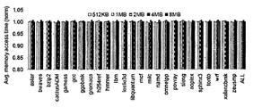
- FIG. 5 is a graph comparing a relative average access time to a conventional technique when a central processing unit accesses main memory through a cache subsystem using a cache memory block replacement method according to an exemplary embodiment of the present invention.
- the present invention has been developed by the Ministry of Knowledge Economy and managed by the Korea Institute of Industrial Technology Evaluation and Management, and the research project "Development of embedded system software source technology for smart devices based on the next generation memory” of SW computing industry source technology development project (government project unique number 1415122825).
- the research was carried out in support of the research project "Design of Embedded Operating System for Smart Devices based on Program Characteristic Analysis" of the Basic Research Project-Mid-sized Researcher Support Project, managed by the Ministry of Education, Science and Technology and managed by the Korea Research Foundation (No. 1345176231). Based on the results.
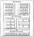
- FIG. 1 is a conceptual diagram illustrating an information processing apparatus having a cache subsystem using a cache memory block replacement method with low write traffic according to an embodiment of the present invention.
- the information processing apparatus 1 has processors 10a and 10b, a cache subsystem 20, and a main memory subsystem 30.
- Processors 10a and 10b may internally have compute cores 11a and 11b and various levels, for example L1 caches 12a and 12b and L2 caches 13a and 13b, respectively.
- L1 caches 12a and 12b or the L2 caches 13a and 13b may be connected such that their respective computation cores 11a and 11b are exclusively accessible.
- Main memory subsystem 30 may include a memory controller 31 and a memory array 32.
- the memory array 32 may be a nonvolatile memory array in which writing is relatively slow compared to reading, such as a phase change (PCM) memory.
- PCM phase change
- the cache subsystem 20 may be configured between the processors 10a and 10b and the main memory subsystem 30, more specifically, for example, between the L2 caches 13a and 13b and the memory controller 31. It provides the lowest level cache (LLC) to alleviate differences in access time requirements and to reduce the time and power spent on accessing a particular main memory block by the processor.
- LLC lowest level cache
- the cache subsystem 20 may include a cache controller 21, an additional information storage 22, and a cache data storage 23, and more specifically, the cache controller 21 may include an access control unit 211.
- the additional information control unit 212 and the replacement control unit 213 may be included.
- cache subsystem 20 may be implemented as part of processor 10a, 10b, both physically and electrically.
- the cache subsystem 20 is implemented physically and electrically independent of the processors 10a, 10b, so that the cache 10a, 10b having multiple compute cores 11a, 11b can share it. It can serve to provide memory space.
- a processor typically processes data or instructions on an address basis, but the frequent use of cache or main memory on an address basis for this purpose requires a high cost, so that a large number of bytes are accessed rather than frequently accessed on an address basis. It is more advantageous to access all at once.
- spatial locality or temporal locality data required by a processor at a particular point in time is often spatially or temporally adjacent, which is called spatial locality or temporal locality.
- the cache exchanges data with the upper cache or processor in line units, and exchanges data with the lower cache or main memory in block units composed of a plurality of lines.
- mapping methods namely, direct mapping, fully associative mapping, and aggregation Methods such as set associative mapping are often used.
- a specific location for storing data blocks of a specific address set obtained from the main memory or the lower cache is determined in advance.
- Direct-mapped caches are fast to fetch because the processor does not waste time looking for a storage location in the cache where a particular word is desired.
- the cache may not be able to store data in the cache even if space remains. It can reduce space utilization.
- Fully associative mapping is a method of storing a block of data from main memory or a lower cache anywhere in the cache.
- the entire cache space is a set of mappings, and the cache space can be fully utilized.
- special search circuitry such as, for example, CAM (Content Addressable Memory), is needed to search for entries in the cache.
- the set associative mapping scheme is a compromise between the direct mapping scheme and the fully associative mapping scheme.
- the set association mapping scheme divides the entire cache storage space into n sets and uses the index field for the data block of the main memory or the lower cache. By mapping to a block in any one mapping set. Data blocks in main memory or lower caches can be placed in any block in a mapping set.
- mapping schemes may be appropriately selected and applied according to the size and speed of the cache, use, level, and the like.
- the cache subsystem 20 may include a cache controller 21, an additional information storage 22, and a cache data storage 23, more specifically, the cache controller 21. May include an access control unit 211, an additional information control unit 212 and a replacement control unit 213.
- the cache controller 21 When there is an access request from the processors 10a and 10b to the cache data storage unit 23, the cache controller 21 reads or writes at a position corresponding to the address to be accessed, and according to the result of the execution, the cache controller 21
- the additional information T managed by the additional information storage unit 22 is set or updated with respect to the cache block of the cache data storage unit 23 indicated.
- the cache block and the additional information are logically paired, but the cache block is physically stored in the cache data storage 23 and the additional information is separately stored in the information storage 22.
- the side information is used by the processor to determine where the desired data is stored in the cache, whether a reference has recently been made to the cache block, whether it is storing valid data, and whether an update has occurred on each unit of data within the cache block. And at least information such as an index or tag field, a reference field (R), a valid bit (V), and an update bit (D), respectively.
- the tag field TAG consists of bits of the upper part of the address and is required to identify whether the word written to a particular storage location in the cache is the word requested by the processor.
- the tag field TAG may also indicate a cache block constituting one set in each way in the n-way set association mapping scheme.
- cache blocks having the same tag in each way form a set, in which data blocks of a specific address range of a lower cache or main memory are mapped to cache blocks belonging to a specific set.
- data blocks within a specific address range from a lower cache or main memory are distributed and stored in n ways with the same tag field TAG.
- the reference field R is needed to indicate whether there was a read access among the words belonging to the corresponding cache block recently.
- the access control unit 211 of the cache control unit 21 if the word stored in the accessed position is a word requested by the processors 10a and 10b, hits together with the stored word. ), Otherwise, miss.
- the additional information control unit 212 sets the reference field R of the cache block containing the address because there was a reference within a predetermined time period with respect to the address.
- the reference field R may consist of one bit, or may consist of a plurality of bits so that a plurality of references can be displayed according to the reference frequency.
- the reference field R is 1 bit information, and incremented by 1 if it is 2 bits or more information.
- the additional information control unit 212 may initialize the reference field R periodically. In this case, if the reference field R contains a non-zero bit, it means that there has been at least one reference since it was initialized.
- the valid bit V may indicate whether the corresponding cache block is storing valid data or is an empty cache block.
- the access control unit 211 of the cache controller 21 may operate to read only the cache block in which the valid bit V is valid or to perform a new write access only in the cache block in which the valid bit V is invalid. have.
- the additional information control unit 212 of the cache control unit 12 sets the valid bit V for the cache block that is effectively write-accessed to valid.
- the update bit D may indicate whether the data written to the corresponding cache block has been updated since the first write.
- update bits are managed block by block, in embodiments of the present invention, update bit D is managed line by line.
- the additional information control unit 212 of the cache control unit 21 can set the update bit D with respect to the line when the existing data stored in the line to be accessed is updated.
- the additional information control unit 212 may include a plurality of updates allocated for each cache block in the additional information storage 22 for each cache block.
- the bits D may be managed.
- the reference field R, the valid bit R, or the tag field TAG may be managed one by one for each cache block in the additional information storage 22.
- the cache subsystem 20 can determine not only whether each block has been updated but also how much has been updated. This information can be used for cache block replacement.
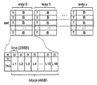
- FIG. 2 illustrates a logical structure of cache blocks in a cache memory block replacement method with low write traffic according to an embodiment of the present invention.
- cache subsystem 20 is illustrated as a cache memory implemented in an n-way set associative mapping scheme.
- the cache subsystem 20 exchanges data in line units with the upper processors 10a and 10b and exchanges data in block units with the memory controller 31 of the lower main memory subsystem 30. .
- the cache subsystem 20 may include a cache block belonging to a set corresponding to a tag field (TAG) value generated from the corresponding address.
- TAG tag field
- the data block is stored in an empty cache block or a victim cache block.
- the upper processors 10a and 10b make cache access requests for specific cache lines in the cache block.
- the cache subsystem 20 may read or update write the corresponding cache line, and change the additional information accordingly.
- the cache block B is composed of 16 cache lines L1, L2, ... L16. If the size of one cache block B is 4 KB, the size of the line L is 256 bytes.
- the columns of these cache blocks B constitute one way, and each way is referred to as way 0, way 1, ... way n.
- the raw (raw) of the cache blocks (B) having a tag field (TAG) value of the same form of the additional information forms a set (set). Data blocks of a specific address of the lower cache or the main memory are mapped to the cache block B constituting one set.
- Each cache block B of the cache data storage 23 is associated one-to-one with each additional information T of the additional information storage 22.
- FIG. 2 the cache block B and the side information T associated with each other are further illustrated.
- One cache block (B) is composed of 16 cache lines (L) by way of example, the additional information (T) is one reference field (R), one valid bit (for each cache block (B) V), one tag field (TAG) and the same number of update bits (D) as cache lines (L).
- the replacement control unit 213 of the cache control unit 21 selects the cache block to be replaced.
- the operation of selecting a cache block to be replaced may be a task of selecting a cache block to be invalidated and returned to an empty cache block, that is, a victim, among cache blocks having data.
- the selection operation of the cache target to be replaced may be initiated according to a predetermined cache replacement event.
- the selection operation of the replacement target cache block may be started.
- replacement is performed according to various cache replacement events, for example, when the number of empty cache blocks is lowered below a predetermined number, or when there are more than a predetermined number of cache blocks having an access frequency below a predetermined frequency in the mapping set.
- the operation of selecting the target cache block may be started.
- Conventional cache block replacement techniques include a Not Recently Used (NRU) technique, a Least Recently Used (LRU) technique, a Re-Reference Interval Prediction (RRIP) technique, and the like. These techniques are techniques for selecting a replacement cache block using a reference field.
- NRU Not Recently Used
- LRU Least Recently Used
- RRIP Re-Reference Interval Prediction
- the NRU technique has one bit reference field for each cache block, sets the reference field to 1 when there is access and hit from the upper cache or processor, and replaces it with a cache block that has not been referenced so far since the initialization of the reference field. This is a technique for selecting a target block.
- the LRU technique or the RRIP technique on the other hand, consists of multiple bits of the reference field, increments the value of the reference field by one when there is access and hit from the upper cache or processor, and has the lowest number of references since the initialization of the reference field. It is a technique of selecting a replacement target block as a cache block for which there are few references.
- the data stored in the cache block to be replaced is data that has been updated one or more times after the initial storage, such an update needs to be reflected in the main memory when the cache memory block is replaced, causing a write demand on the main memory.
- the present invention is based on cache memory block replacement techniques using such a reference field, but additionally, a cache memory block replacement method that minimizes the write operation load on the main memory when replacing the cache memory block.
- the replacement control unit 213 stores the additional information storage unit 22 when a cache miss occurs and an empty cache block is absent, or when a cache block replacement is required within a certain mapping set due to the occurrence of a predetermined cache replacement event.
- Initialization of the reference fields R based on the number of reference fields R and update bits D for each of the cache blocks B belonging to the corresponding mapping set in the additional information T stored in Thereafter, no reference occurs or a relatively low reference occurs, and the replacement target cache block is selected as the cache blocks B with a relatively small number of update bits D.
- the replacement control unit 213 may store the additional information storage unit 22 when cache block replacement is required within a certain mapping set according to occurrence of a predetermined cache replacement event such as generation of a cache miss. Based on the reference field R for each of the cache blocks B belonging to the corresponding mapping set among the additional information T stored in the reference, no reference has occurred or the reference count is relative after initialization of the reference fields R. Select at least one replacement candidate cache block.
- the replacement control unit 213 replaces the replacement based on the update bits D for each of the cache blocks B belonging to the corresponding mapping set among the additional information T stored in the additional information storage 22.
- replacement target cache blocks are selected as cache blocks B having a relatively small number of set update bits D in each replacement candidate cache block.
- the replacement control unit 213 may store additional information stored in the additional information storage unit 22 when cache block replacement is required within a certain mapping set according to occurrence of a predetermined cache replacement event such as occurrence of a cache miss. Based on the update bits D for the respective cache blocks B belonging to the corresponding mapping set among (T), the replacement candidate cache as the cache blocks B having a relatively small number of update bits D. Select blocks.
- the replacement control unit 213 refers to the reference based on the reference field R for each of the cache blocks B belonging to the corresponding mapping set among the additional information T stored in the additional information storage 22. After the initialization of the fields R, at least one cache object to be replaced is selected, in which no reference occurs or the number of references is relatively small.
- the replacement control unit 213 selects the replacement target cache block, if the number of update bits D for the selected replacement target cache block is one or more, the access control unit 211 first stores the replacement target cache block. After transferring the data to the memory controller 31 of the main memory subsystem 30, the data block fetched from the main memory subsystem 30 due to a cache miss, for example, can be written to the selected replacement target cache block. Can be.
- the access control unit 211 may retrieve the data block fetched from the main memory subsystem 30 due to, for example, a cache miss. Can be written to the selected replacement target cache block as it is.
- the additional information control unit 212 can appropriately initialize the additional information T of the cache block B that has been replaced. For example, in the side information T of the newly swapped cache block B, both the reference field R and the update bits D may be initialized to zero.
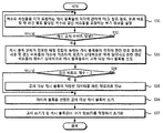
- FIG. 3 is a flowchart illustrating a cache memory block replacement method according to an embodiment of the present invention.
- the cache memory block replacement method of the present invention includes a cache data storage unit 23 having cache blocks each having a plurality of lines, and a cache data storage unit 23 added with respect to respective cache blocks.
- the cache subsystem 20 in step S31, the cache subsystem 20 relates to each of the cache blocks each including a plurality of lines. And setting additional information including a plurality of update bits allocated for each line.
- step S32 the cache subsystem 20 monitors the occurrence of a predetermined cache replacement event, including the occurrence of a cache miss and the absence of an empty cache block.
- step S32 If a predetermined cache replacement event occurs in step S32, the flow advances to step S33, otherwise, the flow returns to step S31.
- step S33 the cache subsystem 20, in the side information T stored in the side information storage 22, refers to each of the cache blocks B belonging to a certain mapping set for which cache block replacement is needed.
- the replacement target cache block is preferably selected as the least cache blocks (B).
- step S33 is based on the reference field R for each of the cache blocks B belonging to the corresponding mapping set among the additional information T, so that the reference after initialization of the reference fields R Selecting at least one replacement candidate cache block as a cache block that has not occurred or has a relatively low number of references, and then updates bits for each cache block B belonging to the corresponding mapping set from the side information T; Selecting the cache targets to be replaced as cache blocks B having a relatively small number of set update bits D in each replacement candidate cache block among the replacement candidate cache blocks. can do.
- step S33 is based on the update bits D for each cache block B belonging to the corresponding mapping set among the additional information T, so that the number of update bits D is relative. Selecting replacement candidate cache blocks as fewer cache blocks B, and then based on the reference field R for each cache block B belonging to the corresponding mapping set among the additional information T, The method may include selecting at least one cache target to be replaced, in which a reference has not occurred since the initialization of the reference fields R or the reference number is relatively small.
- step S34 it is determined whether or not the number of update bits D for the selected replacement target cache block is one or more. In other words, it is determined in step S34 whether the data currently stored in the cache block has been updated since it was first written.
- step S35 the cache subsystem 20 may first transmit the data stored in the replacement target cache block to the outside, in particular to the memory controller 31 of the main memory subsystem 30. have.
- the cache subsystem 20 may write the data block retrieved from the main memory subsystem 30 or the lower cache to the selected replacement target cache block.
- step S34 if the number of update bits for the selected cache block is zero and the corresponding cache block has never been updated, the process proceeds directly to step S36, where the cache subsystem 20 receives the main memory subsystem. Alternatively, the data block fetched from the lower cache may be written to the selected replacement target cache block.
- the cache subsystem 20 may appropriately initialize the additional information T of the cache block B that has been replaced. For example, in the side information T of the newly swapped cache block B, both the reference field R and the update bits D may be initialized to zero.
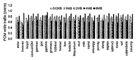
- FIG. 4 is a graph comparing the relative write traffic to the main memory caused by the cache subsystem using the cache memory block replacement method according to an embodiment of the present invention.
- the cache block replacement method according to the existing NRU method and the cache of the present invention with respect to the cache storage configured with 256-byte length lines and 16-way set associative mapping in a commercial dual core processor having L1 cache and L2 cache.
- Each cache simulator was run with a block replacement method.
- the size of the cache was set to 512 KB, 1 MB, 2 MB, 4 MB and 8 MB, respectively.
- the write traffic for the main memory caused by the cache block replacement method using the conventional NRU scheme is based on applications. And at least 50% to 90% depending on cache size. Write traffic decreased by 25% on average.
- the performance degradation or the shortening of lifespan caused by the write traffic can be reduced in nonvolatile memory such as PCM, which has a relatively slow write.
- the effect was different depending on the size of the cache.
- the cache size was 4 MB
- the most effective effect was in terms of reducing the write traffic.
- the cache size was 8 MB
- the size of one mapping set was You can see that it grows so much that it causes more write traffic than when the cache size is 512 KB.
- FIG. 5 is a graph comparing a relative average access time to a conventional technique when a central processing unit accesses main memory through a cache subsystem using a cache memory block replacement method according to an exemplary embodiment of the present invention.
- the apparatus according to the present invention can be embodied as computer readable codes on a computer readable recording medium.
- the computer-readable recording medium includes all kinds of recording devices in which data that can be read by a computer system is stored.
- the recording medium includes, for example, a ROM, a RAM, an optical disk, a magnetic tape, a floppy disk, a hard disk, a nonvolatile memory, and the like.
- the computer readable recording medium can also be distributed over network coupled computer systems so that the computer readable code is stored and executed in a distributed fashion.
Landscapes
- Engineering & Computer Science (AREA)
- Theoretical Computer Science (AREA)
- Physics & Mathematics (AREA)
- General Engineering & Computer Science (AREA)
- General Physics & Mathematics (AREA)
- Memory System Of A Hierarchy Structure (AREA)
Abstract
본 발명의 캐시 서브시스템은 하위 캐시 또는 메인 메모리에서 인출된 데이터 블록을, 적어도 하나의 매핑 집합에 속하며 각각 복수의 라인들을 포함하는 캐시 블록들의 각각에 저장하는 캐시 데이터 저장부, 캐시 블록들의 각각에 관하여 태그, 참조 필드, 유효 비트와, 각 라인 별로 할당된 복수의 갱신 비트들을 포함하는 부가 정보를 저장하는 부가 정보 저장부 및 상위 캐시 또는 프로세서와는 라인 단위로 통신하고 하위 캐시 또는 메인 메모리와는 블록 단위로 통신하며, 소정의 캐시 블록 교체 이벤트가 발생할 경우에, 캐시 블록 교체가 필요한 어떤 매핑 집합에 속하는 각 캐시 블록들에 관하여 부가 정보 저장부에 저장된 부가 정보 내의 참조 필드 및 갱신 비트들의 개수에 기초하여, 캐시 데이터 저장부의 캐시 블록들 중에서 교체 대상 캐시 블록을 선정하며, 선정된 교체 대상 캐시 블록을 교체하는 캐시 제어부를 포함할 수 있다.
Description
본 발명은 캐시 메모리에 관한 것으로, 더욱 상세하게는, 캐시 메모리의 블록 교체 기법에 관한 것이다.
최근 상변화 메모리(PCM) 기술, 자기 저항 메모리(MRAM) 등의 차세대 비휘발성 메모리 기술이 급격하게 발전하면서 곧 상용화될 것으로 예상된다.
차세대 메모리 기술들은 랜덤 액세스, 즉 임의의 주소에 곧바로 접근하여 읽기와 쓰기가 가능한 점에서 현재의 디램 기술을 대체할 수 있고, 비교적 저렴하게 대용량으로 생산될 수 있다는 점에서 현재의 플래시 메모리 기반의 대용량 스토리지 기술도 대체할 수 있어서, 차세대 비휘발성 메모리 기술을 이용한 비휘발성 메모리 소자들을 메인 메모리, 캐시 또는 스토리지로서 최대한 활용하기 위한 파일 관리 기법들도 폭넓게 개발되고 있다.
특히 PCM은 다른 기술에 비해 읽기 속도가 디램에 비견될 정도로 빠르고 저전력이며 집적도가 높아 유력한 기술로 전망되지만, 쓰기 시의 속도가 다소 느리고 전력 소비가 많으며 셀당 1 억번 정도로 쓰기 횟수 제한이 있다.
이러한 이유들로 인하여, 현재로서는 상변화 메모리는 컴퓨터 시스템의 메인 메모리 용도로 곧바로 활용되기는 어렵다고 볼 수 있다. 하지만, 메인 메모리로서의 상변화 메모리 장치 사이에서 적절하게 제어되는 캐시 메모리를 이용한다면, 상변화 메모리는 다른 차세대 비휘발성 메모리 기술과 대등한 경쟁력을 가질 수 있다.
캐시 메모리는 상대적으로 빠른 중앙 처리 장치와 상대적으로 느린 메인 메모리 사이에서 속도 차이의 완충 역할을 할 뿐 아니라, 중앙 처리 장치가 멀리 떨어진 메인 메모리를 대신하여 가까이 있는 캐시 메모리에서 필요한 데이터에 액세스할 수 있게 하기 때문에 속도와 전력 소비를 줄일 수 있다.
다만, 캐시 메모리의 용량은 제한적이므로 캐시 메모리를 효율적으로 사용하기 위해서는 블록들이 좀더 유용하고 적중률이 높은 데이터를 저장할 수 있도록 블록들을 적절히 교체하는 기법이 필요하다.
종래의 캐시 메모리 블록 교체 방법들은 가까운 미래에 참조될 가능성이 낮은 블록을 교체함으로써 캐시 적중률을 높이는 접근 방향을 보여 왔다.
이러한 종래의 캐시 메모리 블록 교체 방법들은, 교체 대상이 된 블록들이 저장 중인 데이터들이 대체로 메인 메모리에 쓰기 연산을 유발한다는 점에서, 상변화 메모리가 메인 메모리인 시스템에 그대로 적용한다면, 메인 메모리에 적지 않은 쓰기 부하를 유발할 수 있고, 이는 읽기에 비해 쓰기가 상대적으로 느린 PCM 메인 메모리 기반의 시스템에서는 상당한 성능 저하와 수명 단축으로 이어질 수 있다.
따라서, 쓰기 트래픽을 절감하는 캐시 메모리 블록 교체 방법이 필요하다.
본 발명이 해결하고자 하는 과제는 쓰기 트래픽이 적은 캐시 메모리 블록 교체 방법 및 이를 이용한 캐시 서브시스템을 가지는 정보 처리 장치를 제공하는 데에 있다.
본 발명의 일 측면에 따른 캐시 서브시스템은,
하위 캐시 또는 메인 메모리에서 인출된 데이터 블록을, 적어도 하나의 매핑 집합에 속하며 각각 복수의 라인들을 포함하는 캐시 블록들의 각각에 저장하는 캐시 데이터 저장부;
상기 캐시 블록들의 각각에 관하여 태그, 참조 필드, 유효 비트와, 각 라인 별로 할당된 복수의 갱신 비트들을 포함하는 부가 정보를 저장하는 부가 정보 저장부; 및
상위 캐시 또는 프로세서와는 라인 단위로 통신하고 상기 하위 캐시 또는 메인 메모리와는 블록 단위로 통신하며, 소정의 캐시 블록 교체 이벤트가 발생할 경우에, 캐시 블록 교체가 필요한 어떤 매핑 집합에 속하는 각 캐시 블록들에 관하여 상기 부가 정보 저장부에 저장된 부가 정보 내의 참조 필드 및 갱신 비트들의 개수에 기초하여, 상기 캐시 데이터 저장부의 캐시 블록들 중에서 교체 대상 캐시 블록을 선정하며, 선정된 교체 대상 캐시 블록을 교체하는 캐시 제어부를 포함할 수 있다.
일 실시예에 따라, 상기 캐시 제어부는
상기 소정의 캐시 교체 이벤트의 발생에 따라 어떤 매핑 집합 내에서 캐시 블록 교체가 필요한 경우에, 상기 부가 정보 저장부에 저장된 부가 정보 중에서 해당 매핑 집합에 속하는 캐시 블록들의 각각에 관한 참조 필드 및 갱신 비트들의 개수에 기초하여, 참조 필드들의 초기화 이후 참조가 일어나지 않았거나 또는 참조가 상대적으로 적게 일어났으면서, 또한 갱신 비트들의 개수가 상대적으로 적은 캐시 블록들으로서 교체 대상 캐시 블록을 선정하도록 동작할 수 있다.
일 실시예에 따라, 상기 캐시 제어부는,
소정의 캐시 교체 이벤트의 발생에 따라 어떤 매핑 집합 내에서 캐시 블록 교체가 필요한 경우에, 상기 부가 정보 저장부에 저장된 부가 정보 중에서 해당 매핑 집합에 속하는 캐시 블록들의 각각에 관한 참조 필드에 기초하여, 참조 필드들의 초기화 이후 참조가 일어나지 않았거나 또는 참조 횟수가 상대적으로 적은 적어도 하나의 교체 후보 캐시 블록들을 선정하고,
상기 부가 정보 저장부에 저장된 부가 정보 중에서 해당 매핑 집합에 속하는 캐시 블록들의 각각에 관한 갱신 비트들에 기초하여, 상기 교체 후보 캐시 블록들 중에서 각 교체 후보 캐시 블록 내의 설정된 갱신 비트들의 개수가 상대적으로 적은 캐시 블록들로서 교체 대상 캐시 블록들을 선정하도록 동작할 수 있다.
일 실시예에 따라, 상기 캐시 제어부는,
소정의 캐시 교체 이벤트의 발생에 따라 어떤 매핑 집합 내에서 캐시 블록 교체가 필요한 경우에, 상기 부가 정보 저장부에 저장된 부가 정보 중에서 해당 매핑 집합에 속하는 캐시 블록들의 각각에 관한 갱신 비트들에 기초하여, 상기 갱신 비트들의 개수가 상대적으로 적은 캐시 블록들로서 교체 후보 캐시 블록들을 선정하고,
상기 부가 정보 저장부에 저장된 부가 정보 중에서 해당 매핑 집합에 속하는 캐시 블록들의 각각에 관한 참조 필드에 기초하여, 참조 필드들의 초기화 이후 참조가 일어나지 않았거나 또는 참조 횟수가 상대적으로 적은 적어도 하나의 교체 대상 캐시 블록들을 선정하도록 동작할 수 있다.
일 실시예에 따라, 상기 소정의 캐시 교체 이벤트는
캐시 미스의 발생 시에 빈 캐시 블록이 부재한 경우, 빈 캐시 블록의 개수가 소정 개수 이하로 낮아지는 경우, 매핑 집합 내에 액세스 빈도가 소정 빈도 이하인 캐시 블록들의 수가 소정 개수 이상 존재할 경우 중 적어도 어느 하나일 수 있다.
일 실시예에 따라, 상기 캐시 제어부는
만약 선정된 교체 대상 캐시 블록에 관한 갱신 비트의 개수가 하나 이상이면, 상기 교체 대상 캐시 블록에 저장된 데이터를 하위 캐시 또는 메인 메모리로 송출한 후에, 새로운 데이터 블록을 선정된 교체 대상 캐시 블록에 쓰기하도록 동작할 수 있다.
일 실시예에 따라, 상기 캐시 제어부는
만약 선정된 교체 대상 캐시 블록에 관한 갱신 비트의 개수가 0이면, 새로운 데이터 블록을 선정된 교체 대상 캐시 블록에 곧바로 쓰기하도록 동작할 수 있다.
일 실시예에 따라, 상기 캐시 제어부는
교체 쓰기가 된 캐시 블록에 관한 부가 정보 중에서 참조 필드 및 갱신 비트들을 초기화하도록 동작할 수 있다.
본 발명의 다른 측면에 따른 캐시 서브시스템을 포함하는 정보 처리 장치는,
프로세서;
메인 메모리 서브시스템; 및
상기 프로세서와 상기 메인 메모리 서브시스템 사이에서 캐시 기능을 제공하는 캐시 서브시스템을 포함하며,
상기 캐시 서브시스템은,
상기 메인 메모리 서브시스템에서 인출된 데이터 블록을, 적어도 하나의 매핑 집합에 속하며 각각 복수의 라인들을 포함하는 캐시 블록들의 각각에 저장하는 캐시 데이터 저장부;
상기 캐시 블록들의 각각에 관하여 태그, 참조 필드, 유효 비트와, 각 라인 별로 할당된 복수의 갱신 비트들을 포함하는 부가 정보를 저장하는 부가 정보 저장부; 및
상기 프로세서와는 라인 단위로 통신하고 상기 메인 메모리 서브시스템과는 블록 단위로 통신하며, 소정의 캐시 블록 교체 이벤트가 발생할 경우에, 캐시 블록 교체가 필요한 어떤 매핑 집합에 속하는 각 캐시 블록들에 관하여 상기 부가 정보 저장부에 저장된 부가 정보 내의 참조 필드 및 갱신 비트들의 수에 기초하여, 상기 캐시 데이터 저장부의 캐시 블록들 중에서 교체 대상 캐시 블록을 선정하며, 선정된 교체 대상 캐시 블록을 교체하는 캐시 제어부를 포함하는 캐시 서브시스템을 포함할 수 있다.
일 실시예에 따라, 상기 메인 메모리 서브시스템은 읽기에 비해 쓰기가 상대적으로 느린 비휘발성 메모리 어레이를 포함할 수 있다.
본 발명의 또 다른 측면에 따른 복수의 라인들을 각각 포함하는 캐시 블록들의 각각에 관하여 부가 정보를 저장하는 캐시 서브시스템의 캐시 블록 교체 방법은,
복수의 라인들을 각각 포함하는 캐시 블록들의 각각에 관하여 태그, 참조 필드, 유효 비트 및 각 라인 별로 할당된 복수의 갱신 비트들을 포함하는 부가 정보를 설정하는 단계;
소정의 캐시 교체 이벤트의 발생을 감시하는 단계;
만약 소정의 캐시 교체 이벤트가 발생한 경우에, 캐시 블록 교체가 필요한 어떤 매핑 집합에 속하는 캐시 블록들의 각각에 관하여 상기 부가 정보 저장부에 저장된 부가 정보 내의 참조 필드 및 갱신 비트들의 개수에 기초하여, 상기 캐시 데이터 저장부의 캐시 블록들 중에서 교체 대상 캐시 블록을 선정하는 단계; 및
선정된 교체 대상 캐시 블록을 교체하는 단계를 포함할 수 있다.
일 실시예에 따라, 상기 교체 대상 캐시 블록을 선정하는 단계는,
상기 소정의 캐시 교체 이벤트의 발생에 따라 어떤 매핑 집합 내에서 캐시 블록 교체가 필요한 경우에, 상기 부가 정보 중에서 해당 매핑 집합에 속하는 캐시 블록들의 각각에 관한 참조 필드 및 갱신 비트들의 개수에 기초하여, 참조 필드들의 초기화 이후 참조가 일어나지 않았거나 또는 참조가 상대적으로 적게 일어났으면서, 또한 갱신 비트들의 개수가 상대적으로 적은 캐시 블록들으로서 교체 대상 캐시 블록을 선정하는 단계를 포함할 수 있다.
일 실시예에 따라, 상기 교체 대상 캐시 블록을 선정하는 단계는,
소정의 캐시 교체 이벤트의 발생에 따라, 어떤 매핑 집합 내에서 캐시 블록 교체가 필요한 경우에, 상기 부가 정보 중에서 해당 매핑 집합에 속하는 캐시 블록들의 각각에 관한 참조 필드에 기초하여, 참조 필드들의 초기화 이후 참조가 일어나지 않았거나 또는 참조 횟수가 상대적으로 적은 적어도 하나의 교체 후보 캐시 블록들을 선정하는 단계; 및
상기 부가 정보 중에서 해당 매핑 집합에 속하는 각 캐시 블록들에 관한 갱신 비트들에 기초하여, 상기 교체 후보 캐시 블록들 중에서 각 교체 후보 캐시 블록 내의 설정된 갱신 비트들의 개수가 상대적으로 적은 캐시 블록들로서 교체 대상 캐시 블록들을 선정하는 단계를 포함할 수 있다.
일 실시예에 따라, 상기 교체 대상 캐시 블록을 선정하는 단계는,
소정의 캐시 교체 이벤트의 발생에 따라 어떤 매핑 집합 내에서 캐시 블록 교체가 필요한 경우에, 상기 부가 정보 중에서 해당 매핑 집합에 속하는 캐시 블록들의 각각에 관한 갱신 비트들에 기초하여, 상기 갱신 비트들의 개수가 상대적으로 적은 캐시 블록들로서 교체 후보 캐시 블록들을 선정하는 단계; 및
상기 부가 정보 중에서 해당 매핑 집합에 속하는 캐시 블록들의 각각에 관한 참조 필드에 기초하여, 참조 필드들의 초기화 이후 참조가 일어나지 않았거나 또는 참조 횟수가 상대적으로 적은 적어도 하나의 교체 대상 캐시 블록들을 선정하는 단계를 포함할 수 있다.
일 실시예에 따라, 상기 소정의 캐시 교체 이벤트는
캐시 미스의 발생 시에 빈 캐시 블록이 부재한 경우, 빈 캐시 블록의 개수가 소정 개수 이하로 낮아지는 경우, 매핑 집합 내에 액세스 빈도가 소정 빈도 이하인 캐시 블록들의 수가 소정 개수 이상 존재할 경우 중 적어도 어느 하나일 수 있다.
일 실시예에 따라, 상기 선정된 교체 대상 캐시 블록을 교체하는 단계는,
만약 선정된 교체 대상 캐시 블록에 관한 갱신 비트의 개수가 하나 이상이면, 상기 교체 대상 캐시 블록에 저장된 데이터를 하위 캐시 또는 메인 메모리로 송출한 후에, 새로운 데이터 블록을 선정된 교체 대상 캐시 블록에 쓰기하는 단계를 포함할 수 있다.
일 실시예에 따라, 상기 선정된 교체 대상 캐시 블록을 교체하는 단계는,
만약 선정된 교체 대상 캐시 블록에 관한 갱신 비트의 개수가 0이면, 새로운 데이터 블록을 선정된 교체 대상 캐시 블록에 곧바로 쓰기하는 단계를 포함할 수 있다.
일 실시예에 따라, 상기 캐시 서브시스템의 캐시 블록 교체 방법은,
교체 쓰기가 된 캐시 블록에 관한 부가 정보 중에서 참조 필드 및 갱신 비트들을 초기화하는 단계를 더 포함할 수 있다.
일 실시예에 따라, 상기 캐시 서브시스템은 상기 프로세서와 상기 메인 메모리 서브시스템 사이에서 캐시 기능을 제공하고,
상기 메인 메모리 서브시스템은 읽기에 비해 쓰기가 상대적으로 느린 비휘발성 메모리 어레이를 포함할 수 있다.
본 발명의 쓰기 트래픽이 적은 캐시 메모리 블록 교체 방법 및 이를 이용한 캐시 서브시스템을 가지는 정보 처리 장치에 따르면, 메인 메모리에 대한 쓰기 트래픽을 적게 유발하는 블록들을 우선으로 교체함으로써 캐시 메모리 블록 교체의 효율을 유지하면서 동시에 메인 메모리에 대한 쓰기 연산량을 감소시킬 수 있다.
본 발명의 쓰기 트래픽이 적은 캐시 메모리 블록 교체 방법 및 이를 이용한 캐시 서브시스템을 가지는 정보 처리 장치에 따르면, 기존의 캐시 메모리 관리 방법과 동질성을 유지하므로 기존의 캐시 메모리 관리 체계와 유연하게 결합될 수 있다.
도 1은 본 발명의 일 실시예에 따른 쓰기 트래픽이 적은 캐시 메모리 블록 교체 방법을 이용한 캐시 서브시스템을 가지는 정보 처리 장치를 예시한 개념도이다.
도 2는 본 발명의 일 실시예에 따른 쓰기 트래픽이 적은 캐시 메모리 블록 교체 방법에서 캐시 블록들의 논리적 구조를 예시한 개념도이다.
도 3은 본 발명의 일 실시예에 따른 캐시 메모리 블록 교체 방법을 예시한 순서도이다.
도 4는 본 발명의 일 실시예에 따른 캐시 메모리 블록 교체 방법을 이용한 캐시 서브시스템이 유발하는 메인 메모리에 대한 상대적인 쓰기 트래픽을 기존 기법에 비교한 그래프이다.
도 5는 본 발명의 일 실시예에 따른 캐시 메모리 블록 교체 방법을 이용한 캐시 서브시스템을 통해 중앙 처리 장치가 메인 메모리에 접근할 경우에 상대적인 평균 액세스 시간을 기존 기법에 비교한 그래프이다.
본문에 개시되어 있는 본 발명의 실시예들에 대해서, 특정한 구조적 내지 기능적 설명들은 단지 본 발명의 실시예를 설명하기 위한 목적으로 예시된 것으로, 본 발명의 실시예들은 다양한 형태로 실시될 수 있으며 본문에 설명된 실시예들에 한정되는 것으로 해석되어서는 아니 된다.
이하, 첨부한 도면들을 참조하여, 본 발명의 바람직한 실시예를 보다 상세하게 설명하고자 한다. 도면상의 동일한 구성요소에 대해서는 동일한 참조부호를 사용하고 동일한 구성요소에 대해서 중복된 설명은 생략한다.
본 발명은 지식경제부에서 주관하고 한국산업기술평가관리원에서 관리하는 SW컴퓨팅 산업 원천기술개발 사업의 "차세대 메모리 기반의 스마트 디바이스용 임베디드 시스템 소프트웨어 원천기술 개발" 연구과제(정부과제고유번호 1415122825호)와 교육과학기술부에서 주관하고 한국연구재단에서 관리하는 기초연구사업-중견연구자지원사업의 "프로그램 특성 분석에 기반한 스마트 디바이스용 임베디드 운영체제 설계" 연구과제(정부과제고유번호 1345176231호)의 지원으로 수행된 연구 결과를 토대로 한다.
도 1은 본 발명의 일 실시예에 따른 쓰기 트래픽이 적은 캐시 메모리 블록 교체 방법을 이용한 캐시 서브시스템을 가지는 정보 처리 장치를 예시한 개념도이다.
도 1을 참조하면, 정보 처리 장치(1)는 프로세서(10a, 10b)와 캐시 서브시스템(20), 메인 메모리 서브시스템(30)을 가진다.
프로세서(10a, 10b)는 각각 연산 코어(11a, 11b)와, 다양한 레벨의, 예를 들어 L1 캐시(12a, 12b) 및 L2 캐시(13a, 13b)를 내부적으로 가질 수 있다. 이러한 프로세서(10a, 10b)에서, L1 캐시(12a, 12b)나 L2 캐시(13a, 13b)는 각각의 연산 코어(11a, 11b)가 독점적으로 액세스할 수 있도록 연결될 수 있다.
메인 메모리 서브시스템(30)은 메모리 컨트롤러(31)와 메모리 어레이(32)를 포함할 수 있다. 이때, 메모리 어레이(32)는 상변화(PCM) 메모리와 같이, 읽기에 비해 쓰기가 상대적으로 느린 비휘발성 메모리 어레이일 수 있다.
캐시 서브시스템(20)은 프로세서(10a, 10b)와 메인 메모리 서브시스템(30) 사이에서, 좀더 구체적으로는 예를 들어 L2 캐시(13a, 13b)와 메모리 컨트롤러(31) 사이에서, 전송 속도 및 액세스 시간 요구 차이를 완화하고, 프로세서가 특정 메인 메모리 블록에 접근하는 데에 소비되는 시간 및 전력을 절감하기 위한 가장 하위 레벨 캐시(LLC: Last Level Cache)를 제공한다.
캐시 서브시스템(20)은 캐시 제어부(21)와 부가 정보 저장부(22) 및 캐시 데이터 저장부(23)를 포함할 수 있고, 좀더 구체적으로, 캐시 제어부(21)는 액세스 제어 유닛(211), 부가 정보 제어 유닛(212)과 교체 제어 유닛(213)을 포함할 수 있다.
실시예에 따라, 캐시 서브시스템(20)은 물리적 내지 전기적으로 프로세서(10a, 10b)의 일부로 구현될 수 있다.
실시예에 따라서, 캐시 서브시스템(20)은 물리적 내지 전기적으로 프로세서(10a, 10b)와 독립적으로 구현되어, 다중 연산 코어(11a, 11b)를 가지는 프로세서(10a, 10b)가 공유할 수 있도록 캐시 메모리 공간을 제공하는 역할을 할 수 있다.
한편, 통상적으로 프로세서는 어드레스 단위로 데이터나 명령어를 처리하지만, 이를 위해 어드레스 단위로 캐시 또는 메인 메모리를 빈번하게 이용하는 것은 높은 비용을 감수해야 하기 때문에 어드레스 단위로 빈번하게 액세스되는 것보다는 다수의 바이트들에 한꺼번에 액세스되는 것이 좀더 유리하다.
또한, 어떤 특정한 시점에 프로세서가 필요한 데이터들은 공간적으로 또는 시간적으로 인접하는 경우가 많은데, 이를 공간 지역성(spatial locality) 또는 시간 지역성(temporal locality)이라고 한다.
이러한 특성들을 이용하여 캐시 성능을 높일 수 있는데, 특정 어드레스의 데이터 또는 코드를 필요로 할 경우에 그에 인접한 데이터들 또는 코드들을 한꺼번에 캐시에 적재한다. 이러한 캐시의 최소 적재 단위를 라인(line) 또는 캐시 라인(cache line)이라고 하는데, 이는 프로세서의 프리페치(prefetch) 기능과 연관되기도 한다.
캐시는 상위 캐시 또는 프로세서와는 라인 단위로 데이터를 주고받고, 하위 캐시 또는 메인 메모리와는 다수의 라인들로 구성된 블록 단위로 데이터를 주고 받는다.
이때, 메인 메모리 또는 하위 캐시에서 가져온 블록 단위 데이터를 캐시 내 저장 위치들 중 어디에 배치하느냐의 문제에 관하여, 세 가지 매핑 방식 즉, 직접 매핑(direct mapping), 완전 연관 매핑(fully associative mapping) 및 집합 연관 매핑(set associative mapping)과 같은 방식이 주로 이용된다.
직접 매핑 방식은 메인 메모리 또는 하위 캐시에서 가져온 특정 어드레스 집합의 데이터 블록들을 저장할 특정 위치를 미리 정해놓은 방식이다. 직접 매핑 방식의 캐시는 프로세서가 원하는 특정 워드가 저장된 캐시 내의 저장 위치를 찾는 데에 시간을 낭비하지 않으므로 페치 속도가 빠르지만, 상황에 따라 캐시 공간이 남아 있어도 캐시에 데이터를 저장하지 못하는 경우가 발생할 수 있어 공간 활용성이 떨어진다.
완전 연관 매핑 방식은 메인 메모리 또는 하위 캐시에서 가져오는 데이터 블록을 캐시 내의 어떠한 위치에도 저장할 수 있는 방식이다. 완전 연관 매핑 방식의 캐시는 캐시 공간 전체가 하나의 매핑 집합으로서, 캐시 공간을 최대한 이용할 수 있지만, 캐시 공간이 상대적으로 클 경우에는 어떤 데이터가 어디에 저장되어 있는지 검색하기 위한 시간이 상당히 소요되기 때문에, 캐시로서의 효용이 떨어질 수 있다. 따라서 완전 연관 매핑 방식에서는, 캐시 내의 엔트리들을 검색하기 위해서는 예를 들어 CAM(Content Addressable Memory)과 같은 특수한 검색 회로가 더 필요하다.
한편, 집합 연관 매핑 방식은 직접 매핑 방식과 완전 연관 매핑 방식의 일종의 절충으로서, 캐시 전체 저장 공간을 n 개의 집합(n-way set)으로 나누고, 메인 메모리 또는 하위 캐시의 데이터 블록을 인덱스 필드를 이용하여 어느 한 매핑 집합 내의 블록에 매핑하는 방식이다. 메인 메모리 또는 하위 캐시의 데이터 블록은 한 매핑 집합 내의 어떠한 블록에도 배치될 수 있다. 완전 연관 매핑 방식은 n=1인 집합 연관 매핑 방식이라고 볼 수도 있다.
이러한 매핑 방식들은 캐시의 크기와 속도, 용도, 레벨 등에 따라 적절하게 선택되어 적용될 수 있다.
매핑 방식의 구현을 위해, 캐시 서브시스템(20)은 캐시 제어부(21)와 부가 정보 저장부(22) 및 캐시 데이터 저장부(23)를 포함할 수 있고, 좀더 구체적으로, 캐시 제어부(21)는 액세스 제어 유닛(211), 부가 정보 제어 유닛(212)과 교체 제어 유닛(213)을 포함할 수 있다.
캐시 제어부(21)는 프로세서(10a, 10b)로부터 캐시 데이터 저장부(23)에 액세스 요청이 있을 경우에, 액세스되는 어드레스에 해당하는 위치에서 읽기 또는 쓰기를 수행하고, 수행 결과에 따라 해당 어드레스가 가리키는 캐시 데이터 저장부(23)의 캐시 블록에 관하여 부가 정보 저장부(22)에서 관리하는 부가 정보(T)를 설정 내지 갱신한다. 다시 말해, 캐시 블록과 부가 정보는 논리적으로 한 쌍을 이루지만, 물리적으로 캐시 블록은 캐시 데이터 저장부(23)에, 부가 정보는 정보 저장부(22)에, 각각 따로 저장된다.
부가 정보는 프로세서가 원하는 데이터가 캐시 내에 저장된 위치, 캐시 블록에 대해 최근에 참조가 일어났는지 여부, 유효한 데이터를 저장하고 있는지 여부, 그리고 캐시 블록 내의 각각의 단위 데이터에 갱신이 일어났는지 여부를 알기 위해, 각각 인덱스(index) 또는 태그 필드(TAG field), 참조 필드(Reference field, R), 유효 비트(Valid bit, V), 갱신 비트(Dirty bit, D)와 같은 정보를 적어도 포함한다.
태그 필드(TAG)는 어드레스의 상위 부분 비트들로 구성되며, 캐시의 특정 저장 위치에 기록된 워드가 프로세서에 의해 요청된 워드인지 여부를 식별하는 데에 필요하다. 특히 태그 필드(TAG)는 n 웨이 집합 연관 매핑 방식에서는 각각의 웨이들에서 하나의 집합을 구성하는 캐시 블록을 지시하는 역할도 할 수 있다. 다시 말해, 각각의 웨이들에서 동일한 태그를 가지는 캐시 블록들이 하나의 집합을 이루는데, 하위 캐시 또는 메인 메모리의 특정 어드레스 범위의 데이터 블록들은 특정 집합 내에 속하는 캐시 블록에 매핑된다. 따라서, 하위 캐시 또는 메인 메모리에서 온 특정 어드레스 범위 내의 데이터 블록은 동일한 태그 필드(TAG)를 가지고 n 개의 웨이에 분산 저장된다.
참조 필드(R)는 최근에 해당 캐시 블록에 속하는 워드들 중에 읽기 액세스가 있었는지 여부를 표시하는 데에 필요하다.
구체적으로, 읽기 액세스의 경우에, 캐시 제어부(21)의 액세스 제어 유닛(211)은, 액세스되는 위치에 저장된 워드가 프로세서(10a, 10b)에 의해 요청된 워드라면, 저장된 워드와 함께 히트(hit)를 리턴하고, 그렇지 않으면 미스(miss)를 리턴한다.
따라서, 부가 정보 제어 유닛(212)은 특정 어드레스에 관하여 히트가 리턴되면, 해당 어드레스에 관하여 소정 시구간 내에 참조가 있었으므로, 해당 어드레스가 포함되는 캐시 블록의 참조 필드(R)를 설정한다.
실시예에 따라, 참조 필드(R)는 하나의 비트로 구성될 수도 있고, 참조 빈도에 따라 복수 회의 참조를 표시할 수 있도록 복수 비트로 구성될 수도 있다.
예를 들어, 참조가 있을 경우에, 참조 필드(R)가 1비트 정보이면 1로 설정하고, 2비트 이상의 정보이면 1씩 증분할 수 있다.
실시예에 따라, 부가 정보 제어 유닛(212)은 주기적으로 참조 필드(R)를 초기화할 수 있다. 이 경우에, 참조 필드(R)가 0이 아닌 비트를 포함하면 초기화된 이후에 적어도 한 번의 참조가 있었음을 의미한다.
유효 비트(V)는 해당 캐시 블록이 유효한 데이터를 저장하고 있는지 또는 비어 있는 캐시 블록인지를 표시할 수 있다.
구체적으로, 캐시 제어부(21)의 액세스 제어 유닛(211)은 유효 비트(V)가 유효한 캐시 블록만 읽기 액세스를 하거나, 유효 비트(V)가 비유효한 캐시 블록에만 새로 쓰기 액세스를 하도록 동작할 수 있다.
또한 캐시 제어부(12)의 부가 정보 제어 유닛(212)은 유효하게 쓰기 액세스된 캐시 블록에 대한 유효 비트(V)를 유효로 설정한다.
갱신 비트(D)는 해당 캐시 블록에 쓰기된 데이터 중에 최초의 쓰기 이후에 갱신된 적이 있는지 여부를 표시할 수 있다.
종래의 캐시 서브시스템들에서 갱신 비트가 블록 별로 관리되는 것과 달리, 본 발명의 실시예들에서 갱신 비트(D)는 라인 별로 관리된다.
구체적으로, 쓰기 액세스의 경우에, 캐시 제어부(21)의 부가 정보 제어 유닛(212)은, 액세스되는 라인에 저장되어 있던 기존 데이터가 갱신되면 해당 라인에 관하여 갱신 비트(D)를 설정할 수 있다.
기존 데이터의 갱신은, 캐시 블록 단위가 아닌, 캐시 블록 내의 라인 별로 일어날 수 있기 때문에, 부가 정보 제어 유닛(212)은 부가 정보 저장부(22) 내에서 각 캐시 블록마다 라인 별로 할당된 복수의 갱신 비트들(D)을 관리할 수 있다. 반면에, 참조 필드(R), 유효 비트(R) 또는 태그 필드(TAG)는 부가 정보 저장부(22) 내에서 각 캐시 블록마다 하나씩 관리될 수 있다.
따라서, 종래의 캐시 서브시스템에서는 각 블록이 갱신되었는지 여부만 판단하고 이용하지만, 본 발명의 실시예들에 따른 캐시 서브시스템(20)은 각 블록이 갱신되었는지 여부뿐 아니라 얼마나 갱신되었는지를 판단할 수 있고, 이러한 정보를 캐시 블록 교체에 이용할 수 있다.
캐시 블록의 구조와 부가 정보에 관하여 좀더 구체적으로 설명하기 위해 도 2를 참조하면, 도 2는 본 발명의 일 실시예에 따른 쓰기 트래픽이 적은 캐시 메모리 블록 교체 방법에서 캐시 블록들의 논리적 구조를 예시한 개념도이다.
도 2에서, 캐시 서브시스템(20)은 n-웨이 집합 연관 매핑 방식으로 구현된 캐시 메모리로 예시된다.
도 2에서 캐시 서브시스템(20)은 상부의 프로세서(10a, 10b)와는 라인 단위로 데이터를 주고받고, 하위의 메인 메모리 서브시스템(30)의 메모리 컨트롤러(31)와는 블록 단위로 데이터를 주고받는다.
다시 말해, 하위의 메인 메모리 서브시스템(30)으로부터 특정 어드레스 군에 속하는 데이터 블록이 읽혀지면, 캐시 서브시스템(20)은 해당 어드레스로부터 생성된 태그 필드(TAG) 값에 상응하는 집합에 속하는 캐시 블록들 중 비어 있는 캐시 블록 또는 희생되는 캐시 블록에 데이터 블록을 저장한다.
반면에 상위의 프로세서(10a, 10b)는 캐시 블록 내의 특정 캐시 라인에 관하여 캐시 액세스 요청을 한다. 캐시 액세스 요청의 종류에 따라, 캐시 서브시스템(20)은 해당 캐시 라인의 읽기 또는 갱신 쓰기를 수행하고, 그에 상응하여 부가 정보의 변경을 수행할 수 있다.
캐시 블록(B)은 16 개의 캐시 라인(L1, L2, ... L16)으로 구성되며, 캐시 블록(B) 하나의 크기가 4 KB라면 라인(L)의 크기는 256 Byte이다. 이러한 캐시 블록들(B)의 열(column)이 각각 하나의 웨이를 구성하며, 각각의 웨이(way)는 way 0, way 1, ... way n으로 지칭된다. 한편, 부가 정보 중 동일한 형태의 태그 필드(TAG) 값을 가지는 캐시 블록들(B)의 행(raw)이 하나의 집합(set)을 구성한다. 하위 캐시 또는 메인 메모리의 특정 어드레스의 데이터 블록들이 하나의 집합을 구성하는 캐시 블록(B)과 매핑된다.
캐시 데이터 저장부(23)의 각각의 캐시 블록(B)은 부가 정보 저장부(22)의 각각의 부가 정보(T)와 1대1로 연계된다.
도 2에서 서로 연계된 캐시 블록(B)과 부가 정보(T)가 더 예시되어 있다.
하나의 캐시 블록(B)은 예시적으로 16 개의 캐시 라인들(L)로 구성되고, 하나의 캐시 블록(B)마다 부가 정보(T)는 하나의 참조 필드(R), 하나의 유효 비트(V), 하나의 태그 필드(TAG) 및 캐시 라인들(L)과 같은 수의 갱신 비트들(D)을 포함한다.
다시 도 1로 돌아와서, 도 2와 같은 구조의 캐시 메모리에 관하여 캐시 블록의 교체(replacement)가 필요할 경우에 캐시 제어부(21)의 교체 제어 유닛(213)이 교체될 캐시 블록을 선정한다.
교체될 캐시 블록을 선정하는 작업은 기존에 데이터를 가진 캐시 블록들 중에서, 적재된 데이터를 무효화하고 빈 캐시 블록으로 반환될, 즉 희생될 캐시 블록(victim)을 선정하는 작업이라고 할 수 있다.
소정의 캐시 교체 이벤트에 따라 교체 대상 캐시 블록의 선정 작업이 개시될 수 있다.
구체적으로, 캐시 읽기 액세스에서 캐시 미스가 발생하여 하위 캐시 또는 메인 메모리에서 데이터 블록을 가져왔는데 캐시 메모리 내에 가져온 데이터 블록을 적재할 빈 캐시 블록이 없을 때에, 교체 대상 캐시 블록의 선정 작업이 개시될 수 있다.
또한 캐시 미스가 일어나지 않더라도, 예를 들어 빈 캐시 블록의 수가 소정 개수 이하로 낮아진다거나, 매핑 집합 내에 액세스 빈도가 소정 빈도 이하인 캐시 블록들의 수가 소정 개수 이상 존재할 경우와 같이, 다양한 캐시 교체 이벤트에 따라 교체 대상 캐시 블록의 선정 작업이 개시될 수 있다.
교체 대상 캐시 블록을 선정하는 작업이 완료되면, 선정된 캐시 블록에 새로운 데이터 블록을 쓰기하는 작업이 수행되며, 이들 두 작업이 캐시 블록의 교체 작업을 구성할 수 있다.
종래의 유력한 캐시 블록 교체 기법으로는, NRU(Not Recently Used) 기법, LRU(Least Recently Used) 기법이나, RRIP(Re-Reference Interval Prediction) 기법 등이 있다. 이들 기법들은 참조 필드를 이용하여 교체 대상 캐시 블록을 선정하는 기법들이다.
NRU 기법은 각 캐시 블록마다 1 비트의 참조 필드를 두고, 상위 캐시 또는 프로세서로부터 액세스 및 히트가 있을 경우에 참조 필드를 1로 설정하며, 참조 필드의 초기화 이후에 현재까지 참조가 없었던 캐시 블록으로서 교체 대상 블록을 선정하는 기법이다.
한편 LRU 기법 또는 RRIP 기법은 참조 필드가 복수 비트로 구성되며, 상위 캐시 또는 프로세서로부터 액세스 및 히트가 있을 경우에 참조 필드의 값을 1씩 증분하며, 참조 필드의 초기화 이후에 현재까지 참조가 가장 적은 또는 앞으로도 참조가 적을 캐시 블록으로서 교체 대상 블록을 선정하는 기법이다.
이때, 교체될 캐시 블록에 저장되어 있던 데이터가 최초 저장 후 한 차례 이상 갱신된 적이 있는 데이터라면, 그러한 갱신은 캐시 메모리 블록 교체 시에 메인 메모리에 반영되어야 하므로, 메인 메모리에 쓰기 수요를 일으킨다.
본 발명은 이러한 참조 필드를 이용하는 캐시 메모리 블록 교체 기법들을 기반으로 하되, 추가적으로, 캐시 메모리 블록 교체 시에 메인 메모리에 대한 쓰기 연산 부하를 최소화하는 캐시 메모리 블록 교체 방법이다.
교체 제어 유닛(213)은 캐시 미스가 발생했는데 빈 캐시 블록이 부재하는 경우에, 또는 소정의 캐시 교체 이벤트의 발생에 따라 어떤 매핑 집합 내에서 캐시 블록 교체가 필요한 경우에, 부가 정보 저장부(22)에 저장된 부가 정보(T)에서 해당 매핑 집합에 속하는 캐시 블록들(B)의 각각에 관한 참조 필드(R) 및 갱신 비트들(D)의 개수에 기초하여, 참조 필드들(R)의 초기화 이후 참조가 일어나지 않았거나 또는 참조가 상대적으로 적게 일어났으면서, 또한 갱신 비트들(D)의 개수가 상대적으로, 바람직하게는 가장 적은 캐시 블록들(B)으로서 교체 대상 캐시 블록을 선정한다.
구체적으로, 일 실시예에서 교체 제어 유닛(213)은, 캐시 미스의 발생과 같은 소정의 캐시 교체 이벤트의 발생에 따라 어떤 매핑 집합 내에서 캐시 블록 교체가 필요한 경우에, 부가 정보 저장부(22)에 저장된 부가 정보(T) 중에서 해당 매핑 집합에 속하는 각 캐시 블록들(B)에 관한 참조 필드(R)에 기초하여, 참조 필드들(R)의 초기화 이후 참조가 일어나지 않았거나 또는 참조 횟수가 상대적으로 적은 적어도 하나의 교체 후보 캐시 블록들을 선정한다.
이어서, 교체 제어 유닛(213)은 부가 정보 저장부(22)에 저장된 부가 정보(T) 중에서 해당 매핑 집합에 속하는 캐시 블록들(B)의 각각에 관한 갱신 비트들(D)에 기초하여, 교체 후보 캐시 블록들 중에서 각 교체 후보 캐시 블록 내의 설정된 갱신 비트들(D)의 개수가 상대적으로 적은 캐시 블록들(B)로서 교체 대상 캐시 블록들을 선정한다.
다른 실시예에서 교체 제어 유닛(213)은 캐시 미스의 발생과 같은 소정의 캐시 교체 이벤트의 발생에 따라 어떤 매핑 집합 내에서 캐시 블록 교체가 필요한 경우에, 부가 정보 저장부(22)에 저장된 부가 정보(T) 중에서 해당 매핑 집합에 속하는 각 캐시 블록들(B)에 관한 갱신 비트들(D)에 기초하여, 갱신 비트들(D)의 개수가 상대적으로 적은 캐시 블록들(B)로서 교체 후보 캐시 블록들을 선정한다.
이어서, 교체 제어 유닛(213)은, 부가 정보 저장부(22)에 저장된 부가 정보(T) 중에서 해당 매핑 집합에 속하는 캐시 블록들(B)의 각각에 관한 참조 필드(R)에 기초하여, 참조 필드들(R)의 초기화 이후 참조가 일어나지 않았거나 또는 참조 횟수가 상대적으로 적은 적어도 하나의 교체 대상 캐시 블록들을 선정한다.
교체 제어 유닛(213)이 교체 대상 캐시 블록을 선정했을 때에, 만약 선정된 교체 대상 캐시 블록에 관한 갱신 비트(D)의 수가 하나 이상이면, 액세스 제어 유닛(211)은 먼저 교체 대상 캐시 블록에 저장된 데이터를 메인 메모리 서브시스템(30)의 메모리 컨트롤러(31)로 전송한 다음에, 예를 들어 캐시 미스로 인해 메인 메모리 서브시스템(30)에서 인출한 데이터 블록을 선정된 교체 대상 캐시 블록에 쓰기할 수 있다.
그렇지 않고 만약 선정된 캐시 블록에 관하여 갱신 비트의 수가 0이어서 해당 캐시 블록이 갱신된 적이 없다면, 액세스 제어 유닛(211)은 예를 들어 캐시 미스로 인해 메인 메모리 서브시스템(30)에서 인출한 데이터 블록을 선정된 교체 대상 캐시 블록에 그대로 쓰기할 수 있다.
나아가, 부가 정보 제어 유닛(212)은 교체 쓰기가 된 캐시 블록(B)의 부가 정보(T)를 적절하게 초기화할 수 있다. 예를 들어, 새로 교체 쓰기된 캐시 블록(B)의 부가 정보(T)에서, 참조 필드(R) 및 갱신 비트들(D)은 모두 0으로 초기화될 수 있다.
도 3은 본 발명의 일 실시예에 따른 캐시 메모리 블록 교체 방법을 예시한 순서도이다.
도 3을 참조하면, 본 발명의 캐시 메모리 블록 교체 방법은, 캐시 서브시스템(20)이 복수의 라인들을 각각 포함하는 캐시 블록들을 가지는 캐시 데이터 저장부(23)와 각각의 캐시 블록들에 관하여 부가 정보를 저장하는 부가 정보 저장부(22)를 포함하는 경우에, 단계(S31)에서, 캐시 서브시스템(20)이 복수의 라인들을 각각 포함하는 캐시 블록들의 각각에 관하여 태그, 참조 필드, 유효 비트 및 각 라인 별로 할당된 복수의 갱신 비트들을 포함하는 부가 정보를 설정하는 단계로부터 시작할 수 있다.
단계(S32)에서, 캐시 서브시스템(20)은 캐시 미스 발생 및 빈 캐시 블록의 부재를 포함하는 소정의 캐시 교체 이벤트의 발생을 감시한다.
만약 단계(S32)에서 소정의 캐시 교체 이벤트가 발생한 경우에는 단계(S33)로 진행하고, 그렇지 않으면 단계(S31)로 돌아간다.
단계(S33)에서, 캐시 서브시스템(20)은 부가 정보 저장부(22)에 저장된 부가 정보(T)에서, 캐시 블록 교체가 필요한 어떤 매핑 집합에 속하는 캐시 블록들(B)의 각각에 관한 참조 필드(R) 및 갱신 비트들(D)의 개수에 기초하여, 참조 필드들(R)의 초기화 이후 참조가 일어나지 않았거나 또는 참조가 상대적으로 적게 일어났으면서, 또한 갱신 비트들(D)의 수가 상대적으로, 바람직하게는 가장 적은 캐시 블록들(B)로서 교체 대상 캐시 블록을 선정한다.
구체적으로, 단계(S33)는, 부가 정보(T) 중에서 해당 매핑 집합에 속하는 캐시 블록들(B)의 각각에 관한 참조 필드(R)에 기초하여, 참조 필드들(R)의 초기화 이후 참조가 일어나지 않았거나 또는 참조 횟수가 상대적으로 적은 캐시 블록으로서 적어도 하나의 교체 후보 캐시 블록들을 선정하는 단계와, 이어서, 부가 정보(T) 중에서 해당 매핑 집합에 속하는 각 캐시 블록들(B)에 관한 갱신 비트들(D)에 기초하여, 교체 후보 캐시 블록들 중에서 각 교체 후보 캐시 블록 내의 설정된 갱신 비트들(D)의 개수가 상대적으로 적은 캐시 블록들(B)로서 교체 대상 캐시 블록들을 선정하는 단계를 포함할 수 있다.
다른 실시예에서, 단계(S33)는 부가 정보(T) 중에서 해당 매핑 집합에 속하는 각 캐시 블록들(B)에 관한 갱신 비트들(D)에 기초하여, 갱신 비트들(D)의 개수가 상대적으로 적은 캐시 블록들(B)로서 교체 후보 캐시 블록들을 선정하는 단계와, 이어서, 부가 정보(T) 중에서 해당 매핑 집합에 속하는 각 캐시 블록들(B)에 관한 참조 필드(R)에 기초하여, 참조 필드들(R)의 초기화 이후 참조가 일어나지 않았거나 또는 참조 횟수가 상대적으로 적은 적어도 하나의 교체 대상 캐시 블록들을 선정하는 단계를 포함할 수 있다.
단계(S34)에서, 선정된 교체 대상 캐시 블록에 관한 갱신 비트(D)의 개수가 하나 이상인지 여부가 판정된다. 다시 말해, 단계(S34)에서 캐시 블록에 현재 저장되어 있는 데이터가 최초로 쓰기된 이후 갱신된 적이 있는지 여부가 판정된다.
단계(S34)의 판정에 따라, 단계(S35)에서 캐시 서브시스템(20)은 먼저 교체 대상 캐시 블록에 저장된 데이터를 외부로, 특히 메인 메모리 서브시스템(30)의 메모리 컨트롤러(31)로 전송할 수 있다.
이어서 단계(S36)에서, 캐시 서브 시스템(20)은 메인 메모리 서브시스템(30) 또는 하위 캐시에서 인출한 데이터 블록을 선정된 교체 대상 캐시 블록에 쓰기할 수 있다.
그렇지 않고 만약 단계(S34)에서, 선정된 캐시 블록에 관하여 갱신 비트의 수가 0이어서 해당 캐시 블록이 갱신된 적이 없다면, 단계(S36)으로 곧바로 진행하여, 캐시 서브 시스템(20)은 메인 메모리 서브시스템(30) 또는 하위 캐시에서 인출한 데이터 블록을 선정된 교체 대상 캐시 블록에 쓰기할 수 있다.
단계(S37)에서, 캐시 서브시스템(20)은 교체 쓰기가 된 캐시 블록(B)의 부가 정보(T)를 적절하게 초기화할 수 있다. 예를 들어, 새로 교체 쓰기된 캐시 블록(B)의 부가 정보(T)에서, 참조 필드(R) 및 갱신 비트들(D)은 모두 0으로 초기화될 수 있다.
도 4는 본 발명의 일 실시예에 따른 캐시 메모리 블록 교체 방법을 이용한 캐시 서브시스템이 유발하는 메인 메모리에 대한 상대적인 쓰기 트래픽을 기존 기법에 비교한 그래프이다.
테스트를 위해, L1 캐시와 L2 캐시를 가지는 상용 듀얼 코어 프로세서에서 256 바이트 길이의 라인과 16 웨이 집합 연관 매핑 방식으로 구성된 캐시 저장부에 관하여 기존의 NRU 기법에 따른 캐시 블록 교체 방법 및 본 발명의 캐시 블록 교체 방법을 가지고 캐시 시뮬레이터를 각각 구동하였다.
본 발명의 캐시 블록 교체 방법의 경우에, 캐시의 크기를 512 KB, 1 MB, 2 MB, 4 MB 및 8 MB로 각각 설정하여 테스트하였다.
도 4를 참조하면, 기존의 NRU 기법을 이용한 캐시 블록 교체 방법에서 유발하는 메인 메모리에 대한 쓰기 트래픽을 기준으로 하였을 때에, 본 발명의 캐시 블록 교체 방법이 유발하는 메인 메모리에 대한 쓰기 트래픽은 어플리케이션들 및 캐시 크기에 따라 적게는 50% 수준에서 90% 수준까지의 범위 내에서 나타났다. 쓰기 트래픽은 평균적으로 25% 정도 감소하였다.
쓰기 트래픽이 감소함에 따라, 쓰기가 상대적으로 느린 PCM과 같은 비휘발성 메모리에서 쓰기 트래픽에 의한 성능 저하나 수명 단축도 줄어드는 효과를 얻을 수 있다.
이때, 캐시의 크기에 따라 그 효과가 달라졌는데, 대체로 캐시 크기가 4 MB인 경우에 대체로 쓰기 트래픽의 감소 측면에서 가장 좋은 효과를 보였으며, 캐시 크기가 8 MB인 경우에는 한 매핑 집합의 크기가 너무 커져서 캐시 크기가 512 KB인 경우보다 오히려 쓰기 트래픽이 더 많이 유발됨을 볼 수 있다.
도 5는 본 발명의 일 실시예에 따른 캐시 메모리 블록 교체 방법을 이용한 캐시 서브시스템을 통해 중앙 처리 장치가 메인 메모리에 접근할 경우에 상대적인 평균 액세스 시간을 기존 기법에 비교한 그래프이다.
도 4의 경우와 동일한 테스트 환경에서, 기존의 NRU 기법을 이용한 캐시 블록 교체 방법에서 측정된 메인 메모리에 대한 액세스 시간을 기준으로 하였을 때에, 본 발명의 캐시 블록 교체 방법을 수행함에 따라 메인 메모리에 대한 액세스 시간은 거의 유사한 것으로 나타났다. 다시 말해 성능 저하는 거의 없었고, 캐시 크기에 따라서는 오히려 수 % 범위에서 성능이 향상되는 경향도 나타났다.
이상과 같이 본 발명은 비록 한정된 실시예와 도면에 의해 설명되었으나, 본 발명이 상기의 실시예에 한정되는 것은 아니며, 이는 본 발명이 속하는 분야에서 통상의 지식을 가진 자라면 이러한 기재로부터 다양한 수정 및 변형이 가능하다. 따라서, 본 발명의 사상은 아래에 기재된 특허청구범위에 의해서만 파악되어야 하고, 이와 균등하거나 또는 등가적인 변형 모두는 본 발명 사상의 범주에 속한다 할 것이다.
또한, 본 발명에 따른 장치는 컴퓨터로 읽을 수 있는 기록매체에 컴퓨터가 읽을 수 있는 코드로서 구현하는 것이 가능하다. 컴퓨터가 읽을 수 있는 기록매체는 컴퓨터 시스템에 의하여 읽혀질 수 있는 데이터가 저장되는 모든 종류의 기록장치를 포함한다. 기록매체는 예를 들어 ROM, RAM, 광학 디스크, 자기 테이프, 플로피 디스크, 하드 디스크, 비휘발성 메모리 등을 포함한다. 또한 컴퓨터가 읽을 수 있는 기록매체는 네트워크로 연결된 컴퓨터 시스템에 분산되어 분산방식으로 컴퓨터가 읽을 수 있는 코드가 저장되고 실행될 수 있다.
Claims (19)
- 하위 캐시 또는 메인 메모리에서 인출된 데이터 블록을, 적어도 하나의 매핑 집합에 속하며 각각 복수의 라인들을 포함하는 캐시 블록들의 각각에 저장하는 캐시 데이터 저장부;상기 캐시 블록들의 각각에 관하여 태그, 참조 필드, 유효 비트와, 각 라인 별로 할당된 복수의 갱신 비트들을 포함하는 부가 정보를 저장하는 부가 정보 저장부; 및상위 캐시 또는 프로세서와는 라인 단위로 통신하고 상기 하위 캐시 또는 메인 메모리와는 블록 단위로 통신하며, 소정의 캐시 블록 교체 이벤트가 발생할 경우에, 캐시 블록 교체가 필요한 어떤 매핑 집합에 속하는 각 캐시 블록들에 관하여 상기 부가 정보 저장부에 저장된 부가 정보 내의 참조 필드 및 갱신 비트들의 개수에 기초하여, 상기 캐시 데이터 저장부의 캐시 블록들 중에서 교체 대상 캐시 블록을 선정하며, 선정된 교체 대상 캐시 블록을 교체하는 캐시 제어부를 포함하는 캐시 서브시스템.
- 청구항 1에 있어서, 상기 캐시 제어부는상기 소정의 캐시 교체 이벤트의 발생에 따라 어떤 매핑 집합 내에서 캐시 블록 교체가 필요한 경우에, 상기 부가 정보 저장부에 저장된 부가 정보 중에서 해당 매핑 집합에 속하는 캐시 블록들의 각각에 관한 참조 필드 및 갱신 비트들의 개수에 기초하여, 참조 필드들의 초기화 이후 참조가 일어나지 않았거나 또는 참조가 상대적으로 적게 일어났으면서, 또한 갱신 비트들의 개수가 상대적으로 적은 캐시 블록들으로서 교체 대상 캐시 블록을 선정하도록 동작하는 것을 특징으로 하는 캐시 서브시스템.
- 청구항 1 또는 청구항 2에 있어서, 상기 캐시 제어부는,소정의 캐시 교체 이벤트의 발생에 따라 어떤 매핑 집합 내에서 캐시 블록 교체가 필요한 경우에, 상기 부가 정보 저장부에 저장된 부가 정보 중에서 해당 매핑 집합에 속하는 캐시 블록들의 각각에 관한 참조 필드에 기초하여, 참조 필드들의 초기화 이후 참조가 일어나지 않았거나 또는 참조 횟수가 상대적으로 적은 적어도 하나의 교체 후보 캐시 블록들을 선정하고,상기 부가 정보 저장부에 저장된 부가 정보 중에서 해당 매핑 집합에 속하는 캐시 블록들의 각각에 관한 갱신 비트들에 기초하여, 상기 교체 후보 캐시 블록들 중에서 각 교체 후보 캐시 블록 내의 설정된 갱신 비트들의 개수가 상대적으로 적은 캐시 블록들로서 교체 대상 캐시 블록들을 선정하도록 동작하는 것을 특징으로 하는 캐시 서브시스템.
- 청구항 1 또는 청구항 2에 있어서, 상기 캐시 제어부는,소정의 캐시 교체 이벤트의 발생에 따라 어떤 매핑 집합 내에서 캐시 블록 교체가 필요한 경우에, 상기 부가 정보 저장부에 저장된 부가 정보 중에서 해당 매핑 집합에 속하는 캐시 블록들의 각각에 관한 갱신 비트들에 기초하여, 상기 갱신 비트들의 개수가 상대적으로 적은 캐시 블록들로서 교체 후보 캐시 블록들을 선정하고,상기 부가 정보 저장부에 저장된 부가 정보 중에서 해당 매핑 집합에 속하는 캐시 블록들의 각각에 관한 참조 필드에 기초하여, 참조 필드들의 초기화 이후 참조가 일어나지 않았거나 또는 참조 횟수가 상대적으로 적은 적어도 하나의 교체 대상 캐시 블록들을 선정하도록 동작하는 것을 특징으로 하는 캐시 서브시스템.
- 청구항 1 또는 청구항 2에 있어서, 상기 소정의 캐시 교체 이벤트는캐시 미스의 발생 시에 빈 캐시 블록이 부재한 경우, 빈 캐시 블록의 개수가 소정 개수 이하로 낮아지는 경우, 매핑 집합 내에 액세스 빈도가 소정 빈도 이하인 캐시 블록들의 수가 소정 개수 이상 존재할 경우 중 적어도 어느 하나인 것을 특징으로 하는 캐시 서브시스템.
- 청구항 1에 있어서, 상기 캐시 제어부는만약 선정된 교체 대상 캐시 블록에 관한 갱신 비트의 개수가 하나 이상이면, 상기 교체 대상 캐시 블록에 저장된 데이터를 하위 캐시 또는 메인 메모리로 송출한 후에, 새로운 데이터 블록을 상기 선정된 교체 대상 캐시 블록에 쓰기하도록 동작하는 것을 특징으로 하는 캐시 서브시스템.
- 청구항 1에 있어서, 상기 캐시 제어부는만약 선정된 교체 대상 캐시 블록에 관한 갱신 비트의 개수가 0이면, 새로운 데이터 블록을 선정된 교체 대상 캐시 블록에 곧바로 쓰기하도록 동작하는 것을 특징으로 하는 캐시 서브시스템.
- 청구항 1에 있어서, 상기 캐시 제어부는교체 쓰기가 된 캐시 블록에 관한 부가 정보 중에서 참조 필드 및 갱신 비트들을 초기화하도록 동작하는 것을 특징으로 하는 캐시 서브시스템.
- 프로세서;메인 메모리 서브시스템; 및상기 프로세서와 상기 메인 메모리 서브시스템 사이에서 캐시 기능을 제공하는 캐시 서브시스템을 포함하며,상기 캐시 서브시스템은,상기 메인 메모리 서브시스템에서 인출된 데이터 블록을, 적어도 하나의 매핑 집합에 속하며 각각 복수의 라인들을 포함하는 캐시 블록들의 각각에 저장하는 캐시 데이터 저장부;상기 캐시 블록들의 각각에 관하여 태그, 참조 필드, 유효 비트와, 각 라인 별로 할당된 복수의 갱신 비트들을 포함하는 부가 정보를 저장하는 부가 정보 저장부; 및상기 프로세서와는 라인 단위로 통신하고 상기 메인 메모리 서브시스템과는 블록 단위로 통신하며, 소정의 캐시 블록 교체 이벤트가 발생할 경우에, 캐시 블록 교체가 필요한 어떤 매핑 집합에 속하는 각 캐시 블록들에 관하여 상기 부가 정보 저장부에 저장된 부가 정보 내의 참조 필드 및 갱신 비트들의 수에 기초하여, 상기 캐시 데이터 저장부의 캐시 블록들 중에서 교체 대상 캐시 블록을 선정하며, 선정된 교체 대상 캐시 블록을 교체하는 캐시 제어부를 포함하는 캐시 서브시스템을 포함하는 것을 특징으로 하는 정보 처리 장치.
- 청구항 9에 있어서, 상기 메인 메모리 서브시스템은 읽기에 비해 쓰기가 상대적으로 느린 비휘발성 메모리 어레이를 포함하는 것을 특징으로 하는 정보 처리 장치.
- 복수의 라인들을 각각 포함하는 캐시 블록들의 각각에 관하여 부가 정보를 저장하는 캐시 서브시스템의 캐시 블록 교체 방법으로서,복수의 라인들을 각각 포함하는 캐시 블록들의 각각에 관하여 태그, 참조 필드, 유효 비트 및 각 라인 별로 할당된 복수의 갱신 비트들을 포함하는 부가 정보를 설정하는 단계;소정의 캐시 교체 이벤트의 발생을 감시하는 단계;만약 소정의 캐시 교체 이벤트가 발생한 경우에, 캐시 블록 교체가 필요한 어떤 매핑 집합에 속하는 캐시 블록들의 각각에 관하여 상기 부가 정보 저장부에 저장된 부가 정보 내의 참조 필드 및 갱신 비트들의 개수에 기초하여, 상기 캐시 데이터 저장부의 캐시 블록들 중에서 교체 대상 캐시 블록을 선정하는 단계; 및선정된 교체 대상 캐시 블록을 교체하는 단계를 포함하는 캐시 서브시스템의 캐시 블록 교체 방법.
- 청구항 11에 있어서, 상기 교체 대상 캐시 블록을 선정하는 단계는,상기 소정의 캐시 교체 이벤트의 발생에 따라 어떤 매핑 집합 내에서 캐시 블록 교체가 필요한 경우에, 상기 부가 정보 중에서 해당 매핑 집합에 속하는 캐시 블록들의 각각에 관한 참조 필드 및 갱신 비트들의 개수에 기초하여, 참조 필드들의 초기화 이후 참조가 일어나지 않았거나 또는 참조가 상대적으로 적게 일어났으면서, 또한 갱신 비트들의 개수가 상대적으로 적은 캐시 블록들으로서 교체 대상 캐시 블록을 선정하는 단계를 포함하는 것을 특징으로 하는 캐시 서브시스템의 캐시 블록 교체 방법.
- 청구항 11 또는 청구항 12에 있어서, 상기 교체 대상 캐시 블록을 선정하는 단계는,소정의 캐시 교체 이벤트의 발생에 따라, 어떤 매핑 집합 내에서 캐시 블록 교체가 필요한 경우에, 상기 부가 정보 중에서 해당 매핑 집합에 속하는 캐시 블록들의 각각에 관한 참조 필드에 기초하여, 참조 필드들의 초기화 이후 참조가 일어나지 않았거나 또는 참조 횟수가 상대적으로 적은 적어도 하나의 교체 후보 캐시 블록들을 선정하는 단계; 및상기 부가 정보 중에서 해당 매핑 집합에 속하는 각 캐시 블록들에 관한 갱신 비트들에 기초하여, 상기 교체 후보 캐시 블록들 중에서 각 교체 후보 캐시 블록 내의 설정된 갱신 비트들의 개수가 상대적으로 적은 캐시 블록들로서 교체 대상 캐시 블록들을 선정하는 단계를 포함하는 것을 특징으로 하는 캐시 서브시스템의 캐시 블록 교체 방법.
- 청구항 11 또는 청구항 12에 있어서, 상기 교체 대상 캐시 블록을 선정하는 단계는,소정의 캐시 교체 이벤트의 발생에 따라 어떤 매핑 집합 내에서 캐시 블록 교체가 필요한 경우에, 상기 부가 정보 중에서 해당 매핑 집합에 속하는 캐시 블록들의 각각에 관한 갱신 비트들에 기초하여, 상기 갱신 비트들의 개수가 상대적으로 적은 캐시 블록들로서 교체 후보 캐시 블록들을 선정하는 단계; 및상기 부가 정보 중에서 해당 매핑 집합에 속하는 캐시 블록들의 각각에 관한 참조 필드에 기초하여, 참조 필드들의 초기화 이후 참조가 일어나지 않았거나 또는 참조 횟수가 상대적으로 적은 적어도 하나의 교체 대상 캐시 블록들을 선정하는 단계를 포함하는 것을 특징으로 하는 캐시 서브시스템의 캐시 블록 교체 방법.
- 청구항 11 또는 청구항 12에 있어서, 상기 소정의 캐시 교체 이벤트는캐시 미스의 발생 시에 빈 캐시 블록이 부재한 경우, 빈 캐시 블록의 개수가 소정 개수 이하로 낮아지는 경우, 매핑 집합 내에 액세스 빈도가 소정 빈도 이하인 캐시 블록들의 수가 소정 개수 이상 존재할 경우 중 적어도 어느 하나인 것을 특징으로 하는 캐시 서브시스템의 캐시 블록 교체 방법.
- 청구항 11에 있어서, 상기 선정된 교체 대상 캐시 블록을 교체하는 단계는,만약 선정된 교체 대상 캐시 블록에 관한 갱신 비트의 개수가 하나 이상이면, 상기 교체 대상 캐시 블록에 저장된 데이터를 하위 캐시 또는 메인 메모리로 송출한 후에, 새로운 데이터 블록을 선정된 교체 대상 캐시 블록에 쓰기하는 단계를 포함하는 것을 특징으로 하는 캐시 서브시스템의 캐시 블록 교체 방법.
- 청구항 11에 있어서, 상기 선정된 교체 대상 캐시 블록을 교체하는 단계는,만약 선정된 교체 대상 캐시 블록에 관한 갱신 비트의 개수가 0이면, 새로운 데이터 블록을 선정된 교체 대상 캐시 블록에 곧바로 쓰기하는 단계를 포함하는 것을 특징으로 하는 캐시 서브시스템의 캐시 블록 교체 방법.
- 청구항 11에 있어서,교체 쓰기가 된 캐시 블록에 관한 부가 정보 중에서 참조 필드 및 갱신 비트들을 초기화하는 단계를 더 포함하는 것을 특징으로 하는 캐시 서브시스템의 캐시 블록 교체 방법.
- 청구항 11에 있어서, 상기 캐시 서브시스템은 상기 프로세서와 상기 메인 메모리 서브시스템 사이에서 캐시 기능을 제공하고,상기 메인 메모리 서브시스템은 읽기에 비해 쓰기가 상대적으로 느린 비휘발성 메모리 어레이를 포함하는 것을 특징으로 하는 캐시 서브시스템의 캐시 블록 교체 방법.
Applications Claiming Priority (2)
| Application Number | Priority Date | Filing Date | Title |
|---|---|---|---|
| KR1020130056082A KR101474842B1 (ko) | 2013-05-16 | 2013-05-16 | 쓰기 트래픽이 적은 캐시 메모리 블록 교체 방법 및 이를 이용한 캐시 서브시스템을 가지는 정보 처리 장치 |
| KR10-2013-0056082 | 2013-05-16 |
Publications (1)
| Publication Number | Publication Date |
|---|---|
| WO2014185652A1 true WO2014185652A1 (ko) | 2014-11-20 |
Family
ID=51898589
Family Applications (1)
| Application Number | Title | Priority Date | Filing Date |
|---|---|---|---|
| PCT/KR2014/003996 Ceased WO2014185652A1 (ko) | 2013-05-16 | 2014-05-07 | 쓰기 트래픽이 적은 캐시 메모리 블록 교체 방법 및 이를 이용한 캐시 서브시스템을 가지는 정보 처리 장치 |
Country Status (2)
| Country | Link |
|---|---|
| KR (1) | KR101474842B1 (ko) |
| WO (1) | WO2014185652A1 (ko) |
Cited By (3)
| Publication number | Priority date | Publication date | Assignee | Title |
|---|---|---|---|---|
| CN111913661A (zh) * | 2020-07-29 | 2020-11-10 | 北京天融信网络安全技术有限公司 | 一种缓存设备替换方法及电子设备 |
| CN112583663A (zh) * | 2020-12-08 | 2021-03-30 | 吉林大学 | 一种基于国产操作系统的自动化网络性能测试方法 |
| CN113641596A (zh) * | 2021-10-18 | 2021-11-12 | 北京壁仞科技开发有限公司 | 缓存管理方法、缓存管理装置、处理器 |
Families Citing this family (6)
| Publication number | Priority date | Publication date | Assignee | Title |
|---|---|---|---|---|
| KR102317248B1 (ko) * | 2014-03-17 | 2021-10-26 | 한국전자통신연구원 | 캐시의 부분연관 재구성을 이용한 캐시 제어 장치 및 캐시 관리 방법 |
| KR20190073660A (ko) | 2017-12-19 | 2019-06-27 | 에스케이하이닉스 주식회사 | 캐시 메모리 장치 및 이를 포함하는 fpga |
| KR101936951B1 (ko) | 2018-04-11 | 2019-01-11 | 주식회사 맴레이 | 메모리 제어 장치 및 이를 포함하는 메모리 시스템 |
| KR102753289B1 (ko) * | 2018-07-17 | 2025-01-14 | 에스케이하이닉스 주식회사 | 캐시 메모리 및 이를 포함하는 메모리 시스템, 캐시 메모리의 축출 방법 |
| US11237970B2 (en) * | 2018-11-07 | 2022-02-01 | Micron Technology, Inc. | Reduce data traffic between cache and memory via data access of variable sizes |
| US20250181240A1 (en) * | 2023-12-05 | 2025-06-05 | Micron Technology, Inc. | Block-efficient write policies for memory devices |
Citations (4)
| Publication number | Priority date | Publication date | Assignee | Title |
|---|---|---|---|---|
| KR20040076313A (ko) * | 2003-02-25 | 2004-09-01 | 이승룡 | 버퍼 캐시 분할 관리 방법 |
| KR20100131054A (ko) * | 2009-06-05 | 2010-12-15 | 세종대학교산학협력단 | 캐쉬 제어기 및 캐쉬 블록 교체 방법 |
| JP2011248389A (ja) * | 2008-09-09 | 2011-12-08 | Panasonic Corp | キャッシュメモリ、キャッシュメモリシステム |
| KR20120084906A (ko) * | 2011-01-21 | 2012-07-31 | 에스케이하이닉스 주식회사 | 비휘발성 메모리 시스템 및 그 관리 방법 |
-
2013
- 2013-05-16 KR KR1020130056082A patent/KR101474842B1/ko active Active
-
2014
- 2014-05-07 WO PCT/KR2014/003996 patent/WO2014185652A1/ko not_active Ceased
Patent Citations (4)
| Publication number | Priority date | Publication date | Assignee | Title |
|---|---|---|---|---|
| KR20040076313A (ko) * | 2003-02-25 | 2004-09-01 | 이승룡 | 버퍼 캐시 분할 관리 방법 |
| JP2011248389A (ja) * | 2008-09-09 | 2011-12-08 | Panasonic Corp | キャッシュメモリ、キャッシュメモリシステム |
| KR20100131054A (ko) * | 2009-06-05 | 2010-12-15 | 세종대학교산학협력단 | 캐쉬 제어기 및 캐쉬 블록 교체 방법 |
| KR20120084906A (ko) * | 2011-01-21 | 2012-07-31 | 에스케이하이닉스 주식회사 | 비휘발성 메모리 시스템 및 그 관리 방법 |
Cited By (4)
| Publication number | Priority date | Publication date | Assignee | Title |
|---|---|---|---|---|
| CN111913661A (zh) * | 2020-07-29 | 2020-11-10 | 北京天融信网络安全技术有限公司 | 一种缓存设备替换方法及电子设备 |
| CN111913661B (zh) * | 2020-07-29 | 2023-07-04 | 北京天融信网络安全技术有限公司 | 一种缓存设备替换方法及电子设备 |
| CN112583663A (zh) * | 2020-12-08 | 2021-03-30 | 吉林大学 | 一种基于国产操作系统的自动化网络性能测试方法 |
| CN113641596A (zh) * | 2021-10-18 | 2021-11-12 | 北京壁仞科技开发有限公司 | 缓存管理方法、缓存管理装置、处理器 |
Also Published As
| Publication number | Publication date |
|---|---|
| KR101474842B1 (ko) | 2014-12-19 |
| KR20140135580A (ko) | 2014-11-26 |
Similar Documents
| Publication | Publication Date | Title |
|---|---|---|
| WO2014185652A1 (ko) | 쓰기 트래픽이 적은 캐시 메모리 블록 교체 방법 및 이를 이용한 캐시 서브시스템을 가지는 정보 처리 장치 | |
| US10592424B2 (en) | Range-based memory system | |
| US6640283B2 (en) | Apparatus for cache compression engine for data compression of on-chip caches to increase effective cache size | |
| US6625714B1 (en) | Parallel distributed function translation lookaside buffer | |
| CN109074320B (zh) | 一种缓存替换方法,装置和系统 | |
| KR20190058316A (ko) | 예측에 기초하여 효율적으로 캐시 라인을 관리하는 시스템 및 방법 | |
| WO2014157817A1 (ko) | 플래시 메모리 기반의 페이지 주소 사상 방법 및 시스템 | |
| WO2013024952A1 (ko) | 메모리 컨트롤러 및 이의 데이터 관리방법 | |
| WO2013042880A2 (ko) | 다양한 블록 크기를 지원하는 주소 사상을 사용하여 플래시 메모리 내에 데이터를 저장하는 방법 및 장치 | |
| JPH04232551A (ja) | 多重仮想アドレス変換方法及び装置 | |
| US11403222B2 (en) | Cache structure using a logical directory | |
| KR20180128489A (ko) | 오브젝트 태그된 메모리 모니터링 방법 및 프로세싱 장치 | |
| JPH07295886A (ja) | 階層メモリ、階層メモリを有するコンピュータ・システムおよび階層メモリ管理方法 | |
| GB2468007A (en) | Data processing apparatus and method dependent on streaming preload instruction. | |
| KR102252377B1 (ko) | 멀티 프로세서 시스템 및 이에 포함된 프로세서의 데이터 관리 방법 | |
| CN107015922B (zh) | 缓存存储器 | |
| WO2015002481A1 (ko) | 플래시 메모리 기반 세가지 상태를 가지는 버퍼 관리 장치 및 방법 | |
| US9483400B2 (en) | Multiplexed memory for segments and pages | |
| US20080301372A1 (en) | Memory access control apparatus and memory access control method | |
| US7093075B2 (en) | Location-based placement algorithms for set associative cache memory | |
| US7219197B2 (en) | Cache memory, processor and cache control method | |
| US5463750A (en) | Method and apparatus for translating virtual addresses in a data processing system having multiple instruction pipelines and separate TLB's | |
| US6810473B2 (en) | Replacement algorithm for a replicated fully associative translation look-aside buffer | |
| KR101102260B1 (ko) | 가상 어드레스 캐시 및 고유 태스크 식별자를 이용하는데이터를 공유하기 위한 방법 | |
| JP2008293472A (ja) | 計算機装置およびそのキャッシュリカバリ方法 |
Legal Events
| Date | Code | Title | Description |
|---|---|---|---|
| 121 | Ep: the epo has been informed by wipo that ep was designated in this application |
Ref document number: 14797730 Country of ref document: EP Kind code of ref document: A1 |
|
| NENP | Non-entry into the national phase |
Ref country code: DE |
|
| 122 | Ep: pct application non-entry in european phase |
Ref document number: 14797730 Country of ref document: EP Kind code of ref document: A1 |