WO2014181514A1 - 光学フィルタ - Google Patents
光学フィルタ Download PDFInfo
- Publication number
- WO2014181514A1 WO2014181514A1 PCT/JP2014/002276 JP2014002276W WO2014181514A1 WO 2014181514 A1 WO2014181514 A1 WO 2014181514A1 JP 2014002276 W JP2014002276 W JP 2014002276W WO 2014181514 A1 WO2014181514 A1 WO 2014181514A1
- Authority
- WO
- WIPO (PCT)
- Prior art keywords
- layer
- optical filter
- dielectric layer
- dielectric
- metal
- Prior art date
- Legal status (The legal status is an assumption and is not a legal conclusion. Google has not performed a legal analysis and makes no representation as to the accuracy of the status listed.)
- Ceased
Links
Images




Classifications
-
- B—PERFORMING OPERATIONS; TRANSPORTING
- B32—LAYERED PRODUCTS
- B32B—LAYERED PRODUCTS, i.e. PRODUCTS BUILT-UP OF STRATA OF FLAT OR NON-FLAT, e.g. CELLULAR OR HONEYCOMB, FORM
- B32B15/00—Layered products comprising a layer of metal
- B32B15/04—Layered products comprising a layer of metal comprising metal as the main or only constituent of a layer, which is next to another layer of the same or of a different material
-
- B—PERFORMING OPERATIONS; TRANSPORTING
- B32—LAYERED PRODUCTS
- B32B—LAYERED PRODUCTS, i.e. PRODUCTS BUILT-UP OF STRATA OF FLAT OR NON-FLAT, e.g. CELLULAR OR HONEYCOMB, FORM
- B32B7/00—Layered products characterised by the relation between layers; Layered products characterised by the relative orientation of features between layers, or by the relative values of a measurable parameter between layers, i.e. products comprising layers having different physical, chemical or physicochemical properties; Layered products characterised by the interconnection of layers
- B32B7/02—Physical, chemical or physicochemical properties
- B32B7/023—Optical properties
-
- G—PHYSICS
- G02—OPTICS
- G02B—OPTICAL ELEMENTS, SYSTEMS OR APPARATUS
- G02B5/00—Optical elements other than lenses
- G02B5/008—Surface plasmon devices
-
- B—PERFORMING OPERATIONS; TRANSPORTING
- B32—LAYERED PRODUCTS
- B32B—LAYERED PRODUCTS, i.e. PRODUCTS BUILT-UP OF STRATA OF FLAT OR NON-FLAT, e.g. CELLULAR OR HONEYCOMB, FORM
- B32B2551/00—Optical elements
Definitions
- Optical filters using pigment-based materials are widely used in color liquid crystal displays and the like, and there are many optical filters mainly corresponding to the visible light region for RGB.
- An optical filter in the visible light region using a dye-based material exhibits good characteristics in terms of both transmittance and the half-value width of the peak of the transmitted wavelength.
- An optical filter using surface plasmon resonance is a structure having a metal layer having a periodic structure, and utilizes surface plasmon resonance generated at the interface between a metal and a dielectric.
- optical filters using surface plasmon resonance it is possible to obtain a desired transmission range by adjusting the periodic length of the periodic structure or devising the shape of holes and dots, or to improve the transmittance by enhancing plasmons. It has been.
- An optical filter using a pigment-based material may not have excellent environmental resistance, for example, the characteristics of the filter may be deteriorated by ultraviolet rays or the like. Moreover, there is a possibility that there is no material exhibiting good transmission characteristics in the near infrared region.
- An optical filter using surface plasmon resonance has the advantages of simple structure and high environmental resistance, but may have poor characteristics such as transmittance and half-width of transmission wavelength peak compared to the above two optical filters. There is.
- An object of the present disclosure is to provide an optical filter using surface plasmon resonance that realizes a narrow transmission band characteristic.
- Substrate 10 is composed of SiO 2. In addition to SiO 2 , any material can be used as long as it has a lower refractive index than that of the high refractive index layer 11.
- the high refractive index layer 11 is made of TiO 2 which is a dielectric having a thickness of 130 nm and a refractive index higher than that of the substrate 10.
- TiO 2 is a dielectric having a thickness of 130 nm and a refractive index higher than that of the substrate 10.
- other materials may be used.
- an oxide such as ZrO 2 or a nitride such as SiN may be used.
- the periodic structure of the metal layer 13 is not limited to that shown in FIG. 2, and may be any periodic structure that can cause surface plasmon resonance.
- the metal dots 15 may be formed in an arbitrary periodic pattern such as a triangular lattice shape in addition to the square lattice shape. Moreover, it is good also as a structure which opened the hole which penetrates the metal layer 13 instead of the metal dot 15 periodically. Also in this case, the holes can be arranged in an arbitrary periodic pattern such as a square lattice or a triangular lattice. Moreover, it is good also as a periodic pattern by providing a stripe-shaped groove
- the transmittance and the half width can be controlled by the thickness of the metal layer 13, the size and shape of the holes and dots.
- the transmittance of 60% or more can be realized by setting the thickness of the metal layer 13 to 200 nm or less, making the holes and dots circular or polygonal, and setting the diameter to 2/3 or less of the period.
- the material of the metal layer 13 is not limited to Al, but may be a single metal such as Au, Ag, Cu, Mg, Zr, In, Sn, Fe, Co, Ni, Rh, Ir, or Pt, or an alloy thereof.
- a conductive oxide such as ITO (indium tin oxide) or zinc oxide can be used. It is desirable to use Al, Au, or an alloy thereof having a high surface plasmon resonance effect.
- a film that prevents reflection of incident light for example, an AR coating film, may be formed on the protective layer 14.
- Equation 1 is expressed as Equation 2 below.
- the light in the propagation mode that satisfies Equation 2 is trapped in the high refractive index layer 11, passes through the high refractive index layer 11, and passes through the substrate 10. It is not incident on. Therefore, the three-layered structure of the substrate 10, the high refractive index layer 11, and the gap layer 12 operates as a wavelength filter that does not transmit a wavelength band that satisfies Equation 2.
- the short wavelength side of the transmission wavelength peak that has not been sufficiently suppressed by wavelength filtering by surface plasmon resonance can be suppressed by wavelength filtering by introducing the high refractive index layer 11. Further, the half-value width of the transmission wavelength peak can be further narrowed by this.
- FIG. 6 is a graph showing the wavelength dependency of the transmittance of the optical filter of Example 1. For comparison, the wavelength dependency of the transmittance is also shown for an optical filter in which the high refractive index layer 11 is omitted from the optical filter of Example 1 (hereinafter referred to as an optical filter of a comparative example). FIG. 6 is obtained by simulation.
- the wavelength dependence of the transmittance of the optical filter of Example 1 is a characteristic having a peak near 860 nm, the transmittance at the peak is 70%, and the half-value width is about 40 nm.
- the wavelength dependency of the transmittance of the optical filter of the comparative example is a characteristic having a peak near 875 nm, and the transmittance at the peak is 70%.
- the half-value width is about 60 nm, and the half-value width is larger than that of the optical filter of Example 1.
- the transmission characteristics of the optical filters of Example 1 and the comparative example are greatly different in the following points.
- the metal layer 23 has two regions 23A and 23B.
- the metal dots 25 are arranged in a square lattice pattern with a predetermined period.
- the metal dots 25 are arranged in a square lattice pattern with a period wider than that of the region 23A.
- Such a pattern can be produced simply by changing the pattern of the photoresist when the metal layer is etched in the manufacturing process of the optical filter of Example 1.
- the transmission wavelength peak when light is incident on the region 23A is different from the transmission wavelength peak when light is incident on the region 23B. Therefore, in the optical filter of Example 2, the transmission wavelength peak can be varied depending on the difference in the incident position of the light in one optical filter.
- the periodic structure of the metal layer 23 is two regions having different periods, but it is naturally possible to have three or more regions having different periods.
- a first dielectric layer made of a dielectric and a position on the first dielectric layer
- a second dielectric layer made of a dielectric having a higher refractive index than that of the first dielectric layer, and a second dielectric layer located on the second dielectric layer and made of a dielectric having a lower refractive index than that of the second dielectric layer.
- the second dielectric layer can be made of any material as long as it has a higher refractive index than the first dielectric layer, and may be an inorganic material or an organic material.
- the second dielectric layer is preferably an oxide or nitride such as titanium oxide (TiO 2 ) or SiN (silicon nitride).
- the optical filter according to the present disclosure can be prevented from transmitting a specific propagation mode.
- the thickness of the second dielectric layer it is possible to suppress the wavelength band that is not desired to be transmitted.
- any material having a refractive index smaller than that of the second dielectric layer can be used, and it may be an inorganic material or an organic material.
- the first dielectric layer and the third dielectric layer may be made of different materials. Since the structure is simple and the cost can be reduced, it is preferable to use the same material.
- SiO 2 , MgF 2 or the like can be used.
- the thickness of the metal layer is designed in accordance with the transmittance of the optical filter of the present disclosure, the half width of the peak of the transmission wavelength, and the like. That is, the transmittance of the optical filter of the present disclosure, the half-value width of the peak of the transmission wavelength, and the like can be controlled by the thickness of the metal layer.
- the metal layer may have a structure including a first region having a periodic structure with a predetermined period and a second region having a periodic structure with a period different from the first region. it can.
- the transmission region can be changed between light transmitted through the first region and light transmitted through the second region.
- a structure may further include a third region having a different period from the first and second regions, a fourth region having a different period from the first to third regions, and the like.
- Wavelength filtering can be performed. Therefore, a narrow band optical filter can be realized.
- a characteristic having a transmission wavelength peak in the near-infrared region, which has been difficult with an optical filter using surface plasmon resonance, can be realized.
Landscapes
- Physics & Mathematics (AREA)
- General Physics & Mathematics (AREA)
- Optics & Photonics (AREA)
- Optical Filters (AREA)
- Laminated Bodies (AREA)
- Optical Modulation, Optical Deflection, Nonlinear Optics, Optical Demodulation, Optical Logic Elements (AREA)
Abstract
光学フィルタは、SiO2からなる基板10と、基板10上に位置する高屈折率層11と、高屈折率層11上に位置するギャップ層12と、ギャップ層12上に位置する金属層13、23と、金属層13、23上に位置する保護層14と、によって構成される。高屈折率層11は、基板10よりも屈折率の高い誘電体であるTiO2からなる。ギャップ層12は、基板10と同様にSiO2からなり、高屈折率層11よりも屈折率が低い。金属層13、23は、平面視において、Alからなる正方形の金属ドット15が正方格子状に配列されたパターンの周期的構造を有している。
Description
本出願は、2013年5月8日に出願された日本国特許出願2013-98442号に基づくものであり、ここにその記載内容を参照により援用する。
本開示は、表面プラズモン共鳴を用いて特定波長帯域の光を選択的に透過させる光学フィルタに関する。
特定の波長帯の光を透過させる光学フィルタは、大きく分けて3種類の光学フィルタがある。第1の種類の光学フィルタは色素系の材料を用いる光学フィルタ(たとえば特許文献1)であり、第2の種類の光学フィルタは誘電体多層膜を用いる光学フィルタ(たとえば特許文献2)であり、第3の種類の光学フィルタは表面プラズモン共鳴を用いる光学フィルタ(たとえば特許文献3~8)である。
色素系の材料を用いた光学フィルタは、カラー液晶ディスプレイなどに広く用いられており、主にRGB用の可視光領域に対応する光学フィルタが多い。色素系材料を用いた可視光領域の光学フィルタは、透過率、透過波長のピークの半値幅ともに良好な特性を示す。
誘電体多層膜を用いた光学フィルタは、屈折率の異なる誘電体膜を交互に所定の膜厚で積層させた構造であり、多くの光学部品に用いられている。誘電体多層膜を用いた光学フィルタは、透過率、透過波長のピークの半値幅ともに良好な特性であり、耐環境性にも優れている。また、誘電体多層膜を用いた光学フィルタは、近赤外領域においても良好な特性が得られる。
表面プラズモン共鳴を用いた光学フィルタは、周期的構造を有する金属層を有した構造であり、金属と誘電体との界面で生じる表面プラズモン共鳴を利用する。表面プラズモン共鳴を用いた光学フィルタにおいては、周期的構造の周期長を調整したり、ホールやドットの形状を工夫することによって、所望の透過域を得たり、プラズモン増強による透過率の向上が試みられている。
本願発明者は、光学フィルタと、光学フィルタに関する技術に関して下記を見出した。
色素系の材料を用いた光学フィルタは、紫外線などによってフィルターの特性が劣化してしまうなど耐環境性に優れていない虞がある。また、近赤外線領域において良好な透過特性を示す材料がない虞がある。
誘電体多層膜を用いた光学フィルタは、良好な特性を得るためには薄膜を10層以上積層させる必要があり、製造に手間がかかり低コスト化が難しい虞がある。また厚さ方向に波長依存性があるため、同一の工程で複数の波長フィルタを作製することができない虞がある。
表面プラズモン共鳴を用いた光学フィルタは、構成が簡単であり、耐環境性も高いという利点があるが、上記2つの光学フィルタに比べて透過率や透過波長のピークの半値幅など特性が悪い虞がある。
本開示の目的は、透過帯域の狭い特性を実現する表面プラズモン共鳴を用いた光学フィルタを提供することである。
本開示の一例によれば、表面プラズモン共鳴を用いて特定の波長帯域の光を選択的に透過させる光学フィルタにおいて、誘電体からなる第1誘電体層と、第1誘電体層上に位置し、第1誘電体層よりも屈折率の高い誘電体からなる第2誘電体層と、第2誘電体層上に位置し、第2誘電体層よりも屈折率の低い誘電体からなる第3誘電体層と、第3誘電体層上に位置し、周期的構造を有した金属からなり、第3誘電体層との界面で表面プラズモン共鳴を生じさせる金属層と、を有する光学フィルタが提供される。
本開示によれば、金属層と第3誘電体層との界面に生じる表面プラズモン共鳴による大域的な波長フィルタリングだけでなく、第2誘電体層を設けたことによる伝搬モードの限定により狭帯域な波長フィルタリングを行うことができる。そのため、狭帯域な光学フィルタを実現することができる。特に、表面プラズモン共鳴を用いた光学フィルタでは従来難しかった近赤外領域に透過波長ピークを有する特性が実現されうる。
本開示についての上記および他の目的、特徴や利点は、添付の図面を参照した下記の詳細な説明から、より明確になる。添付図面において
図1は、実施例1の光学フィルタの構成を示した図であり、
図2は、図1の切断線II-IIにおける、金属ドット15の配列パターンを示した図であり、
図3は、他の金属層13の周期的構造を示した図であり、
図4は、他の金属層13の周期的構造を示した図であり、
図5は、他の金属層13の周期的構造を示した図であり、
図6は、実施例1の光学フィルタの透過率波長依存性を示したグラフであり、
図7は、実施例2の光学フィルタの構成を示した図であり、
図8は、図7の切断線VIII-VIIIにおける、金属ドット25の配列パターンを示した図である。
以下、本開示の具体的な実施例について説明するが、本開示は実施例に限定されるものではない。
(実施例1)
図1は、実施例1の光学フィルタの構成を示した図である。実施例1の光学フィルタは、図1のように、SiO2からなる基板10と、基板10上に位置する高屈折率層11と、高屈折率層11上に位置するギャップ層12と、ギャップ層12上に位置する金属層13と、金属層13上に位置する保護層14と、によって構成されている。この光学フィルタは、その面に垂直に保護層14側から光を入射させ、基板側から出射される光を狭帯域とするものである。基板10、高屈折率層11、ギャップ層12、保護層14は、それぞれ本開示の第1誘電体層、第2誘電体層、第3誘電体層、第4誘電体層に相当している。
(実施例1)
図1は、実施例1の光学フィルタの構成を示した図である。実施例1の光学フィルタは、図1のように、SiO2からなる基板10と、基板10上に位置する高屈折率層11と、高屈折率層11上に位置するギャップ層12と、ギャップ層12上に位置する金属層13と、金属層13上に位置する保護層14と、によって構成されている。この光学フィルタは、その面に垂直に保護層14側から光を入射させ、基板側から出射される光を狭帯域とするものである。基板10、高屈折率層11、ギャップ層12、保護層14は、それぞれ本開示の第1誘電体層、第2誘電体層、第3誘電体層、第4誘電体層に相当している。
基板10は、SiO2からなる。SiO2以外にも、高屈折率層11よりも屈折率の低い誘電体であれば任意の材料を用いることができる。
高屈折率層11は、厚さ130nmで、基板10よりも屈折率の高い誘電体であるTiO2からなる。高屈折率層11は、基板10よりも屈折率の高い誘電体材料であれば、他の材料を用いてもよく、たとえば、ZrO2などの酸化物や、SiNなどの窒化物でよい。高屈折率層11を導入することにより、光の伝搬モードを限定し、所望の帯域の透過率を抑制することができる。詳細については後述する。
ギャップ層12は、基板10と同様にSiO2からなり、高屈折率層11よりも屈折率が低くなっている。ギャップ層12の厚さは50nmである。ギャップ層12は基板10と同じ材料である必要はなく、高屈折率層11よりも屈折率の低い材料であればよい。ただし、基板10と同一の材料を用いることで、高屈折率層11の厚さの設計が容易となり、実施例1の光学フィルタの構成が簡易となり、低コスト化を図ることができる。よって、ギャップ層12は同一材料もしくは誘電率がおよそ等しい材料とすることが望ましい。
金属層13は、図2に示すように、平面視において、Alからなる金属ドット15が正方格子状に配列されたパターンの周期的構造を有している。金属ドット15の形状は直方体であり、平面視において正方形である。金属層13の厚さは100nmである。また、この周期的構造は、周期長(金属ドット15の中心の間隔)は500nm、金属ドット15の大きさ(正方形の一辺の長さ)は250nmである。金属ドット15間の隙間は、保護層14によって埋められている。これにより、金属ドット15が酸化等によって腐食することを防止している。
なお、金属層13の周期的構造は、図2に示したものに限るものではなく、表面プラズモン共鳴を生じうる任意の周期的構造であってよい。たとえば、正方格子状以外にも、三角格子状などの任意の周期的パターンに金属ドット15を形成してもよい。また、金属ドット15ではなく、金属層13を貫通する孔を周期的に開けた構造としてもよい。この場合も孔の配列は正方格子状、三角格子状など任意の周期的パターンとすることができる。また、ストライプ状の溝あるいは凸部を設けることで周期的パターンとしてもよい。金属層13の周期的構造が、ストライプ状の場合は、偏光方向がストライプ方向の光成分については、透過できない点に留意する。ドットあるいは孔の平面視での形状は、円、楕円、正三角形、正方形、正六角形など任意の形状を用いることができ、この形状によっても実施例1の光学フィルタの透過率等を制御することができる。また、ドットあるいは孔の側面は、傾斜を有していてもよい。また、ドット間の隙間や孔は、空洞であってもよいが、実施例1の金属層13のように誘電体(保護層14)によって埋められていることが望ましい。これにより、金属層13の酸化等の腐食を防止するとともに、光学フィルタの物理的な耐久性、安定性を高めることができる。
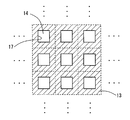
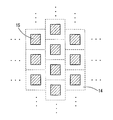
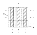
金属層13の周期的構造の一例を図3~5に示す。図3は、金属層13を貫通する正方形の孔17を正方格子状に配列したパターンである。図4は、正方形の金属ドット15を三角格子状に配列したパターンである。図5は、ストライプ状の金属からなる凸部18を設けたパターンである。
たとえば、透過波長のピークを400~2000nmの間にするには、孔またはドットが三角格子状あるいは正方格子状に配列したパターンとし、その周期(ドット間の距離または孔間の距離)を200μm以下とすることで可能となる。また、透過率や半値幅は、金属層13の厚さ、孔およびドットの大きさと形状によって制御可能である。透過率を60%以上とするには、金属層13の厚さを200nm以下とし、孔およびドットを円または多角形とし、その直径を周期の2/3以下とすることで実現できる。
金属層13の材料はAlに限るものではなく、Au、Ag、Cu、Mg、Zr、In、Sn、Fe、Co、Ni、Rh、Ir、Ptなどの金属単体やそれらの合金でよい。金属層13の材料は、ITO(インジウム酸化スズ)、酸化亜鉛、などの導電性酸化物を用いることもできる。表面プラズモン共鳴の効果が高いAl、Auまたはそれらの合金とすることが望ましい。
保護層14は、SiO2からなり、金属層13を封止して酸化等の腐食を防止する。また、保護層14は、光学フィルタの透過率を高める。この構成により、ギャップ層12と金属層13との界面で生じる表面プラズモン共鳴と、金属層13と保護層14との界面で生じる表面プラズモン共鳴を利用することができるため、透過率を高めることができる。保護層14は金属層13上に位置するとともに、金属層13の金属ドット15の隙間を埋めている。保護層14はギャップ層12と異なる材料であってもよい。透過波長の半値幅を狭くするためには、ギャップ層12と保護層14は同一材料とするか、もしくは誘電率がおよそ等しい材料とすることが望ましい。この保護層14は必ずしも必要ではないが、上記利点のため設けることが好ましい。また、金属ドット15の隙間を埋める部材を保護層14と異なるものとしてもよい。
なお、金属層13以外の各構成の材料、つまり基板10、高屈折率層11、ギャップ層12は、無機材料であってもよいし、有機材料であってもよい。フレキシブルな有機材料を用いることで、フィルム状の光学フィルタとすることも可能である。
保護層14上に、入射光の反射を防ぐ膜、たとえばARコート膜を形成してもよい。
実施例1の光学フィルタは、以下の製造方法によって作製する。まず、基板10上に、スパッタや真空蒸着、化学蒸着(CVD)などの方法によって誘電体層11、ギャップ層12を順に形成する。次に、ギャップ層12上に、スパッタや真空蒸着などの方法によって金属層を形成し、その上に電子線(EB)描画、ナノインプリントなどを用いてレジストをパターニングする。そして、誘導結合プラズマ(ICP)エッチングなどを用いて金属層をエッチングすることで、周期的構造を有する金属層13を形成する。その後、金属層13上にスパッタ、真空蒸着、CVDなどの方法によって保護層14を形成する。以上によって実施例1の光学フィルタが作製される。
次に、実施例1の光学フィルタの動作について説明する。
実施例1の光学フィルタは、その光学フィルタの主面に垂直に保護層14表面側から光を入射させ、基板10裏面側から光を透過させて取り出すものである。光を光学フィルタの主面に垂直に、保護層14側から入射させると、保護層14と金属層13の金属ドット15との界面、および金属ドット15とギャップ層12との界面において生じる表面プラズモン共鳴によって、所定の波長帯のみが透過される。つまり、所望の波長に透過率のピークを有した透過特性を有する。
この表面プラズモン共鳴を利用した波長フィルタリングでは、ピークよりも短波長側において十分に透過率を低減することができない虞がある。
この短波長側の光は、高屈折率層11を設けたことで抑制される。高屈折率層11は、高屈折率層11よりも屈折率の低い基板10とギャップ層12との間に設けた層であり、この高屈折率層11を設けたことで、下記数式1を満たす伝搬モードのみが高屈折率層11内を平面方向に伝搬することができる。なお、光学フィルタの主面に垂直に光を入射しているにもかかわらず、高屈折率層11を平面方向に伝搬する光が存在するのは、金属層13の周期的構造による回折のためである。

実施例1の光学フィルタでは、基板10とギャップ層12とで同一材料を用いているため、ε1=ε3であり、数式1は次の数式2のようになる。

この数式2を満たす伝搬モードにおいて許容される波長帯と、表面プラズモン共鳴による波長フィルタリングでの透過波長ピークより左側の帯域とが重なるようにし、かつ、数式2の伝搬モードにおいて禁止される波長帯域(つまり高屈折率層11を透過する波長帯域)と、表面プラズモン共鳴による波長フィルタリングでの透過波長ピークとが重なるように、高屈折率層11の厚さdを設計する。実施例1の光学フィルタでは、高屈折率層11の厚さを130nmとすることで、750~850nmの帯域を透過させないように設計している。これにより、表面プラズモン共鳴による波長フィルタリングで十分に抑制されなかった透過波長ピークの短波長側を、高屈折率層11の導入による波長フィルタリングによって抑制することができる。また、透過波長ピークの半値幅も、これにより一層狭くすることができる。
図6は、実施例1の光学フィルタについて、透過率の波長依存性を示したグラフである。比較のため、実施例1の光学フィルタから高屈折率層11を省いた光学フィルタ(以下、比較例の光学フィルタ)についても透過率の波長依存性を示す。なお、図6はシミュレーションにより求めたものである。
図6のように、実施例1の光学フィルタの透過率の波長依存性は、860nm付近にピークを有した特性であり、そのピークでの透過率は70%、半値幅はおよそ40nmである。一方、比較例の光学フィルタの透過率の波長依存性は、875nm付近にピークを有した特性であり、そのピークでの透過率は70%である。また、半値幅はおよそ60nmであり、実施例1の光学フィルタに比べて半値幅が大きい特性となっている。実施例1と比較例の光学フィルタでは、その透過特性が次の点で大きく異なっている。750~850nmの波長帯域では、実施例1の光学フィルタは10%程度の透過率であるのに対し、比較例の光学フィルタは30~40%の透過率である。この波長帯域において実施例1の光学フィルタが比較例の光学フィルタよりも透過を抑制できているのは、高屈折率層11を導入したことによる波長フィルタリングの効果であることが理解できる。また、半値幅も高屈折率層11の導入により60nmから40nmに狭くなっている。
以上のように、実施例1の光学フィルタは、表面プラズモン共鳴を利用した大域的な波長フィルタリングと、高屈折率層11を設けて伝搬モードを限定することを利用した波長フィルタリングとを行うものであり、この2つの波長フィルタリング動作によって透過率が高く、透過波長のピークの半値幅の狭い特性を得ることができる。また、実施例1の光学フィルタは、透過波長ピークが近赤外領域(700~2500nm)にある。従来、近赤外領域に透過波長ピークを有する狭帯域な光学フィルタは、表面プラズモン共鳴を利用したものでは実現が難しかったが、本開示ではこれを実現することができている。
(実施例2)
図7は、実施例2の光学フィルタの構成を示した図である。実施例2の光学フィルタは、実施例1の光学フィルタの金属層13を金属層23に替えたものであり、他の構成は実施例1の光学フィルタと同様である。
(実施例2)
図7は、実施例2の光学フィルタの構成を示した図である。実施例2の光学フィルタは、実施例1の光学フィルタの金属層13を金属層23に替えたものであり、他の構成は実施例1の光学フィルタと同様である。
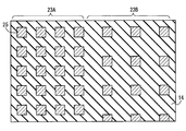
金属層23は、図8に示すように、2つの領域23A、23Bがあり、領域23Aでは、所定の周期で金属ドット25が正方格子状に配列されたパターンとなっており、領域23Bでは、領域23Aの周期よりも広い周期で、金属ドット25が正方格子状に配列されたパターンとなっている。このようなパターンは、実施例1の光学フィルタの製造工程において、金属層をエッチングする際のフォトレジストのパターンを替えるだけで作製することができる。
金属層23の周期的構造の領域23A、23Bでの周期の違いから、光が領域23Aに入射する場合の透過波長ピークと、領域23Bに入射する場合の透過波長ピークとは異なる。したがって、実施例2の光学フィルタは、1つの光学フィルタにおいて、その光の入射位置の違いによって透過波長ピークを異ならせることができる。
なお、実施例2では金属層23の周期的構造を、その周期が異なる2つの領域としたが、周期が互いに異なる3つ以上の領域とすることも当然に可能である。
本開示の光学フィルタは、フォトダイオードを用いたセンサ装置におけるSN比向上などに利用することができる。
本開示の一態様によれば、表面プラズモン共鳴を用いて特定の波長帯域の光を選択的に透過させる光学フィルタにおいて、誘電体からなる第1誘電体層と、第1誘電体層上に位置し、第1誘電体層よりも屈折率の高い誘電体からなる第2誘電体層と、第2誘電体層上に位置し、第2誘電体層よりも屈折率の低い誘電体からなる第3誘電体層と、第3誘電体層上に位置し、周期的構造を有した金属からなり、第3誘電体層との界面で表面プラズモン共鳴を生じさせる金属層と、を有する光学フィルタが提供される。
第2誘電体層は、第1誘電体層よりも屈折率の高い誘電体であれば任意の材料を用いることができ、無機材料であっても有機材料であってもよい。作製の容易さ、低コスト化を考えると、第2誘電体層は酸化チタン(TiO2)、SiN(窒化ケイ素)、などの酸化物や窒化物であることが好ましい。
第2誘電体層を設けることにより、本開示に係る光学フィルタは特定の伝搬モードを透過させないようにできる。第2誘電体層の厚さを適切に設計することで、透過させたくない波長帯域を抑制することができる。
第1、3誘電体層には、第2誘電体層よりも屈折率の小さい任意の材料を用いることができ、無機材料であっても有機材料であってもよい。また、第1誘電体層と第3誘電体層とは異なる材料としてもよい。構造が簡易となり低コスト化を図ることができるので同じ材料とするのがよい。第1誘電体層、第3誘電体層にはSiO2、MgF2などを用いることができる。
金属層は、Al、Au、Ag、Cu、Mg、Zr、In、Sn、Fe、Co、Ni、Rh、Ir、Ptなどの金属単体やそれらの合金を用いることができる。金属層は、ITO(インジウム酸化スズ)、酸化亜鉛、などの導電性酸化物を用いることもできる。特に、表面プラズモン共鳴の効果が高いAl、Auまたはそれらの合金とすることが望ましい。
金属層の周期的構造は、表面プラズモン共鳴を生じうる任意の周期的構造でよく、正方格子状、三角格子状、ストライプ状などの構造とすることができる。また、溝や孔などの凹部によって周期的構造を構成してもよい。ドットなどの凸部によって周期的構造を構成してもよい。ドットや孔の形状は、平面視で、円、楕円、正三角形、正方形、正六角形など任意の形状を用いることができ、その形状によって本開示の光学フィルタの特性を制御することも可能である。また、周期的構造の周期によって、本開示の光学フィルタの透過波長のピークを制御することができる。たとえば、ドットまたは孔を正方格子状あるいは三角格子状に配置して、周期を2μm以下とすれば、透過波長のピークを400~2000nmの間に制御することができる。
凹部によって周期的構造を構成する場合、その凹部は空洞としてもよい。その凹部は、金属層の酸化などによる腐食を防止するため、誘電体によって埋めるようにしてもよい。凸部によって周期的構造を構成する場合も同様である。
また、金属層の厚さは、本開示の光学フィルタの透過率、透過波長のピークの半値幅等に合わせて設計する。つまり、金属層の厚さによって本開示の光学フィルタの透過率や透過波長のピークの半値幅等の制御が可能である。
金属層上には、第4誘電体層をさらに設けてもよい。金属層の酸化等による腐食を防止し、入射光の反射を防止するとともに、第4誘電体層と金属層との界面に生じる表面プラズモン共鳴を利用して本開示の光学フィルタの透過率、透過波長のピークの半値幅を向上させることができる。第4誘電体層は、第3誘電体層と同一材料としてもよい。
本開示の他の態様としては、金属層は、所定周期の周期的構造を有する第1領域と、第1領域とは異なる周期の周期的構造を有する第2領域とを有する構造とすることができる。この構造により、第1領域を透過する光と第2領域を透過する光とで、透過領域を変えることができる。もちろん、第1、2領域とは周期の異なる第3領域、第1~3領域とは周期の異なる第4領域などをさらに有する構造としてもよい。
本開示によれば、金属層と第3誘電体層との界面に生じる表面プラズモン共鳴による大域的な波長フィルタリングだけでなく、第2誘電体層を設けたことによる伝搬モードの限定により狭帯域な波長フィルタリングを行うことができる。そのため、狭帯域な光学フィルタを実現することができる。特に、表面プラズモン共鳴を用いた光学フィルタでは従来難しかった近赤外領域に透過波長ピークを有する特性が実現されうる。
以上、本開示の実施形態、構成、態様を例示したが、本開示に係わる実施形態、構成、態様は、上述した各実施形態、各構成、各態様に限定されるものではない。例えば、異なる実施形態、構成、態様にそれぞれ開示された技術的部を適宜組み合わせて得られる実施形態、構成、態様についても本開示に係わる実施形態、構成、態様の範囲に含まれる。
Claims (7)
- 表面プラズモン共鳴を用いて特定の波長帯域の光を選択的に透過させる光学フィルタにおいて、
誘電体からなる第1誘電体層(10)と、
前記第1誘電体層(10)上に位置し、前記第1誘電体層(10)よりも屈折率の高い誘電体からなる第2誘電体層(11)と、
前記第2誘電体層(11)上に位置し、前記第2誘電体層(11)よりも屈折率の低い誘電体からなる第3誘電体層(12)と、
前記第3誘電体層(12)上に位置し、平面方向に周期的構造を有した金属からなり、前記第3誘電体層(12)との界面で表面プラズモン共鳴を生じさせる金属層(13、23)と、
を有する光学フィルタ。 - 前記金属層(23)は、所定周期の周期的構造を有する第1領域(23A)と、前記第1領域(23A)とは異なる周期の周期的構造を有する第2領域(23B)と、を有する請求項1に記載の光学フィルタ。
- 前記第2誘電体層(11)は、酸化物または窒化物である請求項1または請求項2に記載の光学フィルタ。
- 前記第2誘電体層(11)は、酸化チタン、または窒化ケイ素である請求項1ないし請求項3のいずれか1項に記載の光学フィルタ。
- 前記金属層(13、23)は、Au、Al、またはそれらの合金である請求項1ないし請求項4のいずれか1項に記載の光学フィルタ。
- 前記金属層(13、23)上に位置する第4誘電体層(14)をさらに有する請求項1ないし請求項5のいずれか1項に記載の光学フィルタ。
- 透過帯域が近赤外領域である請求項1ないし請求項6のいずれか1項に記載の光学フィルタ。
Applications Claiming Priority (2)
| Application Number | Priority Date | Filing Date | Title |
|---|---|---|---|
| JP2013-098442 | 2013-05-08 | ||
| JP2013098442A JP6292766B2 (ja) | 2013-05-08 | 2013-05-08 | 光学フィルタ |
Publications (1)
| Publication Number | Publication Date |
|---|---|
| WO2014181514A1 true WO2014181514A1 (ja) | 2014-11-13 |
Family
ID=51867005
Family Applications (1)
| Application Number | Title | Priority Date | Filing Date |
|---|---|---|---|
| PCT/JP2014/002276 Ceased WO2014181514A1 (ja) | 2013-05-08 | 2014-04-23 | 光学フィルタ |
Country Status (2)
| Country | Link |
|---|---|
| JP (1) | JP6292766B2 (ja) |
| WO (1) | WO2014181514A1 (ja) |
Cited By (4)
| Publication number | Priority date | Publication date | Assignee | Title |
|---|---|---|---|---|
| JP2014219546A (ja) * | 2013-05-08 | 2014-11-20 | 株式会社豊田中央研究所 | 光学フィルタ |
| CN105842768A (zh) * | 2016-04-28 | 2016-08-10 | 西安应用光学研究所 | 反0.532μm及1.064μm、透0.6μm-0.9μm光谱分光膜的膜系结构 |
| CN108983457A (zh) * | 2018-08-10 | 2018-12-11 | 南方科技大学 | 一种颜色可调谐的液晶彩色滤光片 |
| CN110412668A (zh) * | 2019-08-07 | 2019-11-05 | 太原理工大学 | 一种产生多重表面晶格共振的结构及其应用 |
Families Citing this family (5)
| Publication number | Priority date | Publication date | Assignee | Title |
|---|---|---|---|---|
| WO2016125843A1 (ja) * | 2015-02-04 | 2016-08-11 | 凸版印刷株式会社 | 表示体、および、表示体の観察方法 |
| JP6641738B2 (ja) * | 2015-02-04 | 2020-02-05 | 凸版印刷株式会社 | 表示体、および、表示体の観察方法 |
| JP2018045156A (ja) * | 2016-09-15 | 2018-03-22 | 凸版印刷株式会社 | 表示体、および、表示体の製造方法 |
| JP6805668B2 (ja) * | 2016-09-15 | 2020-12-23 | 凸版印刷株式会社 | 表示体、表示体付きデバイス、および、表示体の製造方法 |
| JP2023502444A (ja) * | 2019-11-21 | 2023-01-24 | 華為技術有限公司 | 波長選択フィルタ、及び波長選択フィルタを製造する方法 |
Citations (3)
| Publication number | Priority date | Publication date | Assignee | Title |
|---|---|---|---|---|
| JP2010009025A (ja) * | 2008-05-30 | 2010-01-14 | Canon Inc | 光学フィルタ |
| JP2010170085A (ja) * | 2008-12-26 | 2010-08-05 | Canon Inc | 光学素子、及びこれを用いたイメージセンサ、撮像装置 |
| WO2011139785A2 (en) * | 2010-04-27 | 2011-11-10 | The Regents Of The University Of Michigan | Display device having plasmonic color filters and photovoltaic capabilities |
Family Cites Families (1)
| Publication number | Priority date | Publication date | Assignee | Title |
|---|---|---|---|---|
| JP6292766B2 (ja) * | 2013-05-08 | 2018-03-14 | 株式会社豊田中央研究所 | 光学フィルタ |
-
2013
- 2013-05-08 JP JP2013098442A patent/JP6292766B2/ja not_active Expired - Fee Related
-
2014
- 2014-04-23 WO PCT/JP2014/002276 patent/WO2014181514A1/ja not_active Ceased
Patent Citations (3)
| Publication number | Priority date | Publication date | Assignee | Title |
|---|---|---|---|---|
| JP2010009025A (ja) * | 2008-05-30 | 2010-01-14 | Canon Inc | 光学フィルタ |
| JP2010170085A (ja) * | 2008-12-26 | 2010-08-05 | Canon Inc | 光学素子、及びこれを用いたイメージセンサ、撮像装置 |
| WO2011139785A2 (en) * | 2010-04-27 | 2011-11-10 | The Regents Of The University Of Michigan | Display device having plasmonic color filters and photovoltaic capabilities |
Cited By (6)
| Publication number | Priority date | Publication date | Assignee | Title |
|---|---|---|---|---|
| JP2014219546A (ja) * | 2013-05-08 | 2014-11-20 | 株式会社豊田中央研究所 | 光学フィルタ |
| CN105842768A (zh) * | 2016-04-28 | 2016-08-10 | 西安应用光学研究所 | 反0.532μm及1.064μm、透0.6μm-0.9μm光谱分光膜的膜系结构 |
| CN108983457A (zh) * | 2018-08-10 | 2018-12-11 | 南方科技大学 | 一种颜色可调谐的液晶彩色滤光片 |
| CN108983457B (zh) * | 2018-08-10 | 2021-12-03 | 南方科技大学 | 一种颜色可调谐的液晶彩色滤光片 |
| CN110412668A (zh) * | 2019-08-07 | 2019-11-05 | 太原理工大学 | 一种产生多重表面晶格共振的结构及其应用 |
| CN110412668B (zh) * | 2019-08-07 | 2021-10-19 | 太原理工大学 | 一种产生多重表面晶格共振的结构及其应用 |
Also Published As
| Publication number | Publication date |
|---|---|
| JP6292766B2 (ja) | 2018-03-14 |
| JP2014219546A (ja) | 2014-11-20 |
Similar Documents
| Publication | Publication Date | Title |
|---|---|---|
| JP6292766B2 (ja) | 光学フィルタ | |
| JP7356291B2 (ja) | 偏光板及び光学機器 | |
| US9261753B2 (en) | Spectrum filtering for visual displays and imaging having minimal angle dependence | |
| Kim et al. | Generation of reflection colors from metal–insulator–metal cavity structure enabled by thickness-dependent refractive indices of metal thin film | |
| US10302995B2 (en) | High reflectivity LCOS device | |
| US7688512B2 (en) | Transmissive diffraction grating, and spectral separation element and spectroscope using the same | |
| Lee et al. | Omnidirectional flexible transmissive structural colors with high‐color‐purity and high‐efficiency exploiting multicavity resonances | |
| JP5605368B2 (ja) | 光学素子、光源装置及び投射型表示装置 | |
| US9513415B2 (en) | Optical filter configured to transmit light of a predetermined wavelength | |
| JP5280654B2 (ja) | 透過型回折格子、並びに、それを用いた分光素子及び分光器 | |
| JP2012027221A (ja) | ワイヤーグリッド偏光子 | |
| EP3023833B1 (en) | Color filter-integrated polarizer and method of manufacturing the same | |
| WO2012105555A1 (ja) | 波長選択フィルタ素子、その製造方法及び画像表示装置 | |
| US12487468B2 (en) | Reflection-asymmetric metal grating polarization beam splitter | |
| CN107949484A (zh) | 具有亚波长光栅的防伪元件 | |
| KR101575760B1 (ko) | 광차단 영역을 가진 자동정렬형 컬러 필터 어레이 및 이의 제조 방법 | |
| JP6577641B2 (ja) | 偏光板及びその製造方法、並びに光学機器 | |
| US20150022893A1 (en) | Diffraction Grating and Method for the Production Thereof | |
| CN113189690A (zh) | 偏光板、光学设备和偏光板的制造方法 | |
| JP2015191230A (ja) | 共振素子 | |
| CN110998383B (zh) | 偏振片和光学设备 | |
| JP5084603B2 (ja) | 偏光子及び液晶プロジェクタ | |
| CN109975910B (zh) | 偏振光板及其制造方法以及光学设备 | |
| KR101891913B1 (ko) | 투과형 구조색 필터 및 이의 제조방법 | |
| JP6228435B2 (ja) | 光学フィルタ、およびその製造方法 |
Legal Events
| Date | Code | Title | Description |
|---|---|---|---|
| 121 | Ep: the epo has been informed by wipo that ep was designated in this application |
Ref document number: 14794868 Country of ref document: EP Kind code of ref document: A1 |
|
| NENP | Non-entry into the national phase |
Ref country code: DE |
|
| 122 | Ep: pct application non-entry in european phase |
Ref document number: 14794868 Country of ref document: EP Kind code of ref document: A1 |