WO2014174886A1 - タッチパネルおよびタッチパネル付き表示装置 - Google Patents
タッチパネルおよびタッチパネル付き表示装置 Download PDFInfo
- Publication number
- WO2014174886A1 WO2014174886A1 PCT/JP2014/054451 JP2014054451W WO2014174886A1 WO 2014174886 A1 WO2014174886 A1 WO 2014174886A1 JP 2014054451 W JP2014054451 W JP 2014054451W WO 2014174886 A1 WO2014174886 A1 WO 2014174886A1
- Authority
- WO
- WIPO (PCT)
- Prior art keywords
- touch panel
- intersection
- unit
- drive
- length
- Prior art date
- Legal status (The legal status is an assumption and is not a legal conclusion. Google has not performed a legal analysis and makes no representation as to the accuracy of the status listed.)
- Ceased
Links
Images







Classifications
-
- G—PHYSICS
- G06—COMPUTING OR CALCULATING; COUNTING
- G06F—ELECTRIC DIGITAL DATA PROCESSING
- G06F3/00—Input arrangements for transferring data to be processed into a form capable of being handled by the computer; Output arrangements for transferring data from processing unit to output unit, e.g. interface arrangements
- G06F3/01—Input arrangements or combined input and output arrangements for interaction between user and computer
- G06F3/03—Arrangements for converting the position or the displacement of a member into a coded form
- G06F3/041—Digitisers, e.g. for touch screens or touch pads, characterised by the transducing means
- G06F3/0416—Control or interface arrangements specially adapted for digitisers
- G06F3/04166—Details of scanning methods, e.g. sampling time, grouping of sub areas or time sharing with display driving
-
- G—PHYSICS
- G06—COMPUTING OR CALCULATING; COUNTING
- G06F—ELECTRIC DIGITAL DATA PROCESSING
- G06F3/00—Input arrangements for transferring data to be processed into a form capable of being handled by the computer; Output arrangements for transferring data from processing unit to output unit, e.g. interface arrangements
- G06F3/01—Input arrangements or combined input and output arrangements for interaction between user and computer
- G06F3/03—Arrangements for converting the position or the displacement of a member into a coded form
- G06F3/041—Digitisers, e.g. for touch screens or touch pads, characterised by the transducing means
- G06F3/0412—Digitisers structurally integrated in a display
-
- G—PHYSICS
- G06—COMPUTING OR CALCULATING; COUNTING
- G06F—ELECTRIC DIGITAL DATA PROCESSING
- G06F3/00—Input arrangements for transferring data to be processed into a form capable of being handled by the computer; Output arrangements for transferring data from processing unit to output unit, e.g. interface arrangements
- G06F3/01—Input arrangements or combined input and output arrangements for interaction between user and computer
- G06F3/03—Arrangements for converting the position or the displacement of a member into a coded form
- G06F3/041—Digitisers, e.g. for touch screens or touch pads, characterised by the transducing means
- G06F3/044—Digitisers, e.g. for touch screens or touch pads, characterised by the transducing means by capacitive means
- G06F3/0445—Digitisers, e.g. for touch screens or touch pads, characterised by the transducing means by capacitive means using two or more layers of sensing electrodes, e.g. using two layers of electrodes separated by a dielectric layer
-
- G—PHYSICS
- G06—COMPUTING OR CALCULATING; COUNTING
- G06F—ELECTRIC DIGITAL DATA PROCESSING
- G06F3/00—Input arrangements for transferring data to be processed into a form capable of being handled by the computer; Output arrangements for transferring data from processing unit to output unit, e.g. interface arrangements
- G06F3/01—Input arrangements or combined input and output arrangements for interaction between user and computer
- G06F3/03—Arrangements for converting the position or the displacement of a member into a coded form
- G06F3/041—Digitisers, e.g. for touch screens or touch pads, characterised by the transducing means
- G06F3/044—Digitisers, e.g. for touch screens or touch pads, characterised by the transducing means by capacitive means
- G06F3/0446—Digitisers, e.g. for touch screens or touch pads, characterised by the transducing means by capacitive means using a grid-like structure of electrodes in at least two directions, e.g. using row and column electrodes
-
- G—PHYSICS
- G06—COMPUTING OR CALCULATING; COUNTING
- G06F—ELECTRIC DIGITAL DATA PROCESSING
- G06F3/00—Input arrangements for transferring data to be processed into a form capable of being handled by the computer; Output arrangements for transferring data from processing unit to output unit, e.g. interface arrangements
- G06F3/01—Input arrangements or combined input and output arrangements for interaction between user and computer
- G06F3/03—Arrangements for converting the position or the displacement of a member into a coded form
- G06F3/041—Digitisers, e.g. for touch screens or touch pads, characterised by the transducing means
- G06F3/047—Digitisers, e.g. for touch screens or touch pads, characterised by the transducing means using sets of wires, e.g. crossed wires
-
- G—PHYSICS
- G06—COMPUTING OR CALCULATING; COUNTING
- G06F—ELECTRIC DIGITAL DATA PROCESSING
- G06F2203/00—Indexing scheme relating to G06F3/00 - G06F3/048
- G06F2203/041—Indexing scheme relating to G06F3/041 - G06F3/045
- G06F2203/04111—Cross over in capacitive digitiser, i.e. details of structures for connecting electrodes of the sensing pattern where the connections cross each other, e.g. bridge structures comprising an insulating layer, or vias through substrate
Definitions
- the present invention relates to a touch panel and a display device with a touch panel, and more particularly to a capacitive touch panel and a display device with a touch panel.
- one pulse period is selected from a plurality of pulse periods prepared in advance, and a synchronization signal (horizontal synchronization signal Hsync) including a series of pulses appearing in the selected pulse period is disclosed.
- a synchronization signal horizontal synchronization signal Hsync
- a display unit that performs display based on a synchronization signal
- a touch detection unit that performs a touch detection operation based on the synchronization signal.
- the electrode of the touch panel is formed of a transparent conductive film such as ITO (Indium Tin Oxide). Since ITO has a higher electrical resistance than metal, it is necessary to lengthen the measurement time of the capacitance in order to accurately measure the capacitance. Therefore, the time required for measuring the capacitance of the entire touch panel also becomes long, and the responsiveness decreases. On the other hand, it is not preferable to use a metal electrode because the electrode is visually recognized by an observer.
- ITO Indium Tin Oxide
- An object of the present invention is to obtain a configuration of a touch panel that can shorten the time required for measuring the capacitance of the entire touch panel.
- the touch panel disclosed herein charges the intersection capacitance of the intersection of the drive electrode and the sensor electrode in a drive period according to a control unit and a sensor unit including a plurality of drive electrodes and a plurality of sensor electrodes intersecting each other.
- a measurement unit that measures the capacitance of the intersection capacitance, a region determination unit that divides the sensor unit into a plurality of regions, and determines which region of the plurality of regions each of the intersection capacitances belongs to;
- a signal generation unit configured to generate the control signal so that the length of the drive period differs according to the determination result of the region determination unit.
- FIG. 1 is a cross-sectional view showing a schematic configuration of a display device with a touch panel according to an embodiment of the present invention.
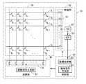
- FIG. 2 is a functional block diagram showing a functional configuration of the touch panel according to the first embodiment of the present invention.
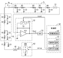
- FIG. 3 is a diagram showing a part of the configuration of the touch panel according to the first embodiment of the present invention as an equivalent circuit.
- FIG. 4 is a signal waveform diagram when the touch panel according to the first embodiment of the present invention measures the capacitance of the intersection capacitance C i, j .
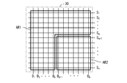
- FIG. 5 is a diagram schematically illustrating an example of how the sensor unit is divided by the region determination unit.
- FIG. 6 is a diagram schematically illustrating another example of how the sensor unit is divided by the region determination unit.
- FIG. 5 is a diagram schematically illustrating an example of how the sensor unit is divided by the region determination unit.
- FIG. 7 is a functional block diagram showing a functional configuration of the touch panel according to the second embodiment of the present invention.
- FIG. 8A is a waveform diagram showing the relationship between the horizontal synchronization signal Hsync and the control signal in the area AR1.
- FIG. 8B is a waveform diagram showing the relationship between the horizontal synchronization signal Hsync and the control signal in the area AR2.
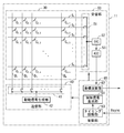
- FIG. 9 is a functional block diagram showing a functional configuration of the touch panel according to the third embodiment of the present invention.
- FIG. 10 is a diagram schematically illustrating an example of how the sensor unit is divided by the region determination unit.
- FIG. 11 is a functional block diagram showing a functional configuration of a touch panel according to the fourth embodiment of the present invention.
- FIG. 12 is a diagram schematically illustrating an example of how the sensor unit is divided by the region determination unit.
- FIG. 13 is a plan view showing an example of a specific configuration of the touch panel.
- 14 is a cross-sectional view taken along line XIV-XIV in FIG.
- FIG. 15 is an exploded perspective view showing another example of the specific configuration of the touch panel.
- 16 is a cross-sectional view taken along line XVI-XVI in FIG.
- FIG. 17 is a diagram schematically illustrating an example of how the sensor unit is divided by the region determination unit.
- FIG. 18A is a waveform diagram showing the relationship between the horizontal synchronization signal Hsync and the control signal in the area AR1.
- FIG. 18B is a waveform diagram showing the relationship between the horizontal synchronization signal Hsync and the control signal in the area AR2.
- a touch panel includes a sensor unit including a plurality of drive electrodes and a plurality of sensor electrodes intersecting each other, and an intersection capacitance of intersections of the drive electrodes and the sensor electrodes in a drive period according to a control signal.
- a measurement unit that measures the capacitance of the intersection capacitance by charging and a region that divides the sensor unit into a plurality of regions and determines to which region of the plurality of regions each of the intersection capacitances belongs
- a determination unit and a signal generation unit that generates the control signal so that the length of the drive period differs according to the determination result of the region determination unit (first configuration).
- the measurement unit measures the capacitance of the intersection capacitance by charging the intersection capacitance.
- the time required to fully charge the intersection capacity varies depending on the location of the intersection capacity.
- charge time can be changed by the area
- the signal generation unit includes another region including an intersection capacitance having a time constant larger than the intersection capacitance belonging to the region, in the length of the drive period in any one of the plurality of regions.
- the drive period may be shorter than the drive period (second configuration).
- the timing adjustment unit that receives a synchronization signal from the outside and adjusts the control signal based on the synchronization signal (third configuration).
- the measurement unit discharges the intersection capacitance in a reset period according to the control signal
- the signal generation unit is configured to respond to a determination result of the region determination unit.
- the control signal is preferably generated so that the length of the reset period is different (fourth configuration).
- the measurement time for each intersection capacity can be set more appropriately. Therefore, the overall measurement time can be further shortened.
- the signal generation unit generates the control signal so that the sum of the length of the reset period and the length of the drive period is one horizontal period or less in one of the plurality of regions. In another one of the plurality of regions, the control signal may be generated such that the sum of the length of the reset period and the length of the drive period is longer than one horizontal period (fifth configuration).
- the measurement unit may measure the intersection capacity in a dot-sequential manner (sixth configuration).
- the number of circuits for measuring the intersection capacitance can be reduced, so that power consumption can be reduced.
- the measurement unit may measure the intersection capacitance line-sequentially (seventh configuration).
- the intersection capacity can be measured in parallel, the measurement time can be further shortened.
- a display device with a touch panel includes a liquid crystal display panel and the touch panel having any one of the first to seventh configurations.
- FIG. 1 is a cross-sectional view illustrating a schematic configuration of a display device 1 with a touch panel according to an embodiment of the present invention.
- the display device with a touch panel 1 includes a touch panel 10, a liquid crystal display panel 20, and a backlight unit 25.
- the touch panel 10 is disposed so as to overlap the surface of the liquid crystal display panel 20 opposite to the backlight 25 side.
- the touch panel 10 is bonded to the liquid crystal display device 20 by OCA (Optical Clear Adhesive).
- the touch panel 10 includes a tempered glass substrate and a group of electrodes formed on one surface of the substrate, which will be described in detail later.
- the touch panel 10 is disposed such that the surface on which the electrode group is formed is on the liquid crystal display panel 20 side.
- the substrate of the touch panel 10 also serves as a cover glass of the display device 1 with a touch panel. That is, the touch panel 10 is a cover glass integrated touch panel.
- the liquid crystal display panel 20 includes a TFT (Thin Film Transistor) substrate 21, a CF (Color Filter) substrate 22, a liquid crystal 23, and a sealing material 24.
- the TFT substrate 21 and the CF substrate 22 are disposed so as to face each other.
- a sealing material 24 is formed on the peripheral edge of the surface where the TFT substrate 21 and the CF substrate 22 face each other, and a liquid crystal 23 is sealed between the TFT substrate 21 and the CF substrate 22.
- the TFT substrate 21 includes a plurality of pixel electrodes.
- the liquid crystal display panel 20 controls the orientation of the liquid crystal 23 by controlling the potentials of these pixel electrodes. As a result, the liquid crystal display panel 20 controls the behavior of light emitted from the backlight unit 25 to express gradation.
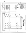
- FIG. 2 is a functional block diagram showing a functional configuration of the touch panel 10 according to the first embodiment of the present invention.
- the touch panel 10 includes a sensor unit 30, a measurement unit (a transmission unit 40 and a reception unit 50), and a control unit 60.
- the sensor unit 30 includes m drive electrodes D 1 to D m and n sensor electrodes S 1 to S n (m and n are positive integers). And drive electrodes D 1 ⁇ D m, the sensor electrodes S 1 ⁇ S n, are arranged to cross each other. Thus, the intersection of the drive electrodes D 1 ⁇ D m and the sensor electrodes S 1 ⁇ S n, intersection capacitance is formed.
- intersection capacitance formed at the intersection of the i-th drive electrode D i (i is an integer from 1 to m) and the j-th sensor electrode S j (j is an integer from 1 to n) is referred to as an intersection capacitance C. Refer to i and j .
- the capacitance of the intersection capacitance C i, j changes when a finger or a stylus pen contacts or approaches the sensor unit 30. Therefore, by measuring the capacitance of the intersection capacitance C i, j , the coordinates of the object that has touched or approached the sensor unit 30 can be obtained.
- the control unit 60 controls the measurement unit (the transmission unit 40 and the reception unit 50) to measure the capacitance of the intersection capacitance C i, j of the sensor unit 30.
- the transmission unit 40 includes a multiplexer 41 and a drive signal generation unit 42.
- the multiplexer 41 selects one electrode from the drive electrodes D 1 to D m and connects it to the drive signal generator 42.
- the drive signal generation unit 42 generates a drive signal and supplies it to the electrode selected by the multiplexer 41.
- the receiver 50 includes a multiplexer 51, a current-voltage converter (IVC (I / V Converter)) 52, and an analog / digital converter (ADC (A / D Converter)) 53.
- Multiplexer 51 selects one electrode from the sensor electrodes S 1 ⁇ S n, connected to IVC52.
- the IVC 52 receives a signal from the electrode selected by the multiplexer 51, converts the received signal from a current to a voltage, and supplies it to the ADC 53.
- the ADC 53 converts the received signal from an analog signal to a digital signal and supplies the signal to the control unit 60.
- control unit 60 can measure the intersection capacitance of the intersection of the electrode selected by the multiplexer 41 and the electrode selected by the multiplexer 51.
- the controller 60 scans all the drive electrodes D 1 to D m and all the sensor electrodes sensor electrodes S 1 to S n to measure n ⁇ m intersection capacitances.
- the controller 60 may be configured to measure the intersection capacitance for each drive electrode, or may be configured to measure the intersection capacitance for each sensor electrode. That is, the control unit 60 is configured to measure the intersection capacity in the order of C 1,1 to C 1, n , C 2,1 to C 2, n ,..., C m, 1 to C m, n. There may be a configuration in which C 1,1 to C m, 1 , C 1,2 to C m, 2 ,..., C 1, n to C m, n are measured in this order. . Or the structure which measures in arbitrary orders different from these may be sufficient.
- the control unit 60 includes a control signal generation unit 61 and a coordinate calculation unit 62.
- the control signal generator 61 generates a control signal for controlling the transmitter 40 and the receiver 50.
- the control signal generator 61 generates different control signals according to the location of the intersection capacitance C i, j to be measured. Detailed operation of the control signal generator 61 will be described later.
- the coordinate calculation unit 62 receives a value related to the capacitance of the intersection capacitance C i, j from the reception unit 50.
- the coordinate calculation unit 62 includes a storage device (not shown) and stores values sequentially supplied from the reception unit 50.
- the coordinate calculation unit 62 performs a predetermined calculation based on the distribution of values stored in the storage device, and calculates the coordinates of an object that has touched or approached the sensor unit 30.
- the coordinate calculation unit 62 supplies the calculated coordinates to the outside of the touch panel 10.
- FIG. 3 is a diagram showing a part of the configuration of the touch panel 10 as an equivalent circuit. More specifically, FIG. 3 is a diagram illustrating an i-th drive electrode D i , a j-th sensor electrode S j, and a circuit connected to these extracted as an equivalent circuit.
- the drive electrodes D i can be expressed as a multi-stage connected RC circuit.
- R1 is the resistance of the wiring between the drive electrode Di and the drive signal generation circuit 42
- C1 is the capacitance of the same wiring.
- R2 is a resistance per unit length of the drive electrode D i
- C2 is a parasitic capacitance per unit length of the drive electrode D i .
- the sensor electrode S j can be expressed as an RC circuit connected in multiple stages.
- R3 is a resistance per unit length of the sensor electrode Sj
- C3 is a parasitic capacitance per unit length of the sensor electrode Sj
- R4 is the resistance of the wiring between the sensor electrode Sj and the IVC 52
- C4 is the capacitance of the same wiring.
- the drive signal generation unit 42 includes a power supply VDD and a changeover switch 421.
- the changeover switch 421 switches the connection destination of the multiplexer 41 between the power supply VDD and the ground (GND) based on the logic signal drive supplied from the control unit 60. More specifically, the changeover switch 421 connects the multiplexer 41 to the power supply VDD when the logic signal drive is at high level, and connects the multiplexer 41 to GND when the logic signal drive is at low level.
- IVC52 is an integration circuit with a reset switch. That is, the IVC 52 includes an operational amplifier 521, an integration capacitor Cs, and a reset switch 522.
- the inverting input terminal of the operational amplifier 521 is connected in parallel to the sensor electrode Sj and one electrode of the integration capacitor Cs.
- the non-inverting input terminal of the operational amplifier 521 is connected to the ground.
- the output terminal of the operational amplifier 521 is connected in parallel with the other electrode of the integration capacitor Cs and the ADC 53.
- the reset switch 522 is connected to two electrodes of the integration capacitor Cs.
- the reset switch 522 opens and closes based on the logic signal reset supplied from the control unit 60. More specifically, the reset switch 522 is turned on when the logic signal reset is at a high level and turned off when the logic signal reset is at a low level.
- the control signal generation unit 61 includes an area determination unit 611 and a signal generation unit 612.
- the region determining unit 611 divides the sensor unit 30 into two or more regions, and determines to which region the intersection capacitance C i, j to be measured belongs.
- the area determination unit 611 supplies the determination result to the signal generation unit 612.
- the signal generation unit 612 generates a control signal including the logic signal drive and the logic signal reset based on the determination result of the region determination unit 611.
- FIG. 4 is a signal waveform diagram when the touch panel 10 measures the capacitance of the intersection capacitance C i, j .
- Vin is a voltage supplied to the drive electrode D i from the driving signal generation circuit 42.
- Vc is a voltage applied to the intersection capacitance C i, j .
- Vout is a voltage output from the IVC 52 to the ADC 53.
- the control signal generation unit 61 sets the logic signal drive to a low level (low) and the logic signal reset to a high level (high).
- Vin becomes GND
- the intersection capacitance C i, j is discharged, and Vc decreases.
- the reset switch 522 is turned on, the integration capacitor Cs is discharged, and Vout becomes GND.
- the control signal generation unit 61 sets the logic signal drive to high level (high) and the logic signal reset to low level (low).
- Vin becomes VDD
- the intersection capacitance C i, j is charged, and Vc increases.
- a transient current flows through the IVC 52.
- the IVC 52 integrates the transient current and outputs it as Vout.
- the controller 60 samples the value of Vout immediately before the drive period t2 ends.
- Vout is expressed by the following equation.
- Vout ⁇ C i, j ⁇ VDD / Cs
- Cs is the capacitance of the integration capacitor Cs
- C i, j is the capacitance of the intersection capacitance C i, j . Since the values of VDD and Cs are known, C i, j can be obtained by measuring Vout.
- the lengths of the reset period t1 it is preferable to set the time intersection capacitance C i, j is sufficiently discharged.
- the time during which the intersection capacitance C i, j is sufficiently charged and discharged and the time during which sufficient transient current is supplied to the IVC 53 vary depending on the location of the intersection capacitance C i, j . Accordingly, the preferred lengths of the reset period t1 and the drive period t2 vary depending on the location of the intersection capacitance C i, j .
- the length of the path from the drive signal generator 42 to the intersection capacitance C i, j, and the intersection capacitance C i from the drive signal generating unit 42, the length of the path to reach the IVC52 via j is an intersection It depends on the location of the capacity C i, j .
- the path for measuring the intersection capacitance C 1,1 is the longest
- the path for measuring the intersection capacitance C m, n is the shortest.
- the longer the path from the drive signal generator 42 to the intersection capacitance C i, j the longer it takes to charge / discharge the intersection capacitance C i, j .
- the length of the reset period t1 and the drive period t2 can be changed according to the location of the intersection capacitance C i, j . That is, the signal generation unit 612 of the control signal generation unit 61 sets the reset period t1 and the drive period t2 to different lengths according to the determination result supplied from the region determination unit 611.
- the signal generation unit 612 sets the length of the drive period t2 in any one of the plurality of areas to the drive period in another area including the intersection capacitance having a time constant larger than the intersection capacitance belonging to the area.
- the length is shorter than the length of t2.
- the signal generation unit 612 is configured so that the signal generation unit 612 includes an intersection capacitance having a length of the reset period t1 in any one of the plurality of regions including an intersection capacitance having a time constant larger than the intersection capacitance belonging to the region. It is shorter than the length of the reset period t1 in the region.
- FIG. 5 is a diagram schematically illustrating an example of how the sensor unit 30 is divided by the region determination unit 611.
- the region determination unit 611 divides the sensor unit 30 into a region AR1 where i ⁇ p or j ⁇ q and a region AR2 where p + 1 ⁇ i and q + 1 ⁇ j.
- p is an integer larger than 1 and smaller than m
- q is an integer larger than 1 and smaller than n.
- the area AR1 includes an intersection capacity having a larger time constant (takes more time for charging / discharging) than any intersection capacity belonging to the area AR2. That is, among the intersection capacitances belonging to the area AR2, the intersection capacitance having the largest time constant is C p + 1, q + 1 .
- the area AR1 includes an intersection capacitance (for example, C 1,1 ) having a larger time constant.
- the region determination unit 611 determines whether the intersection capacitance C i, j to be measured belongs to the region AR1 or the region AR2, and supplies the determination result to the signal generation unit 612.
- the signal generation unit 612 makes the length of the drive period t2 of the control signal in the area AR1 longer than the length of the drive period t2 of the control signal in the area AR2. Further, the signal generation unit 612 makes the length of the control signal reset period t1 in the area AR1 longer than the length of the control signal reset period t1 in the area AR2.
- the length of the reset period t1 is shorter than the length of the drive period t2. For this reason, the length of the reset period t1 may be constant in all regions, and only the length of the drive period t2 may be changed according to the region.
- the signal generation unit 612 sets the lengths of the reset period t1 and the drive period t2 of the control signal in the area AR1 to the intersection capacitance C farthest from the transmission unit 40 and the reception unit 50 among the intersection capacitances belonging to the area AR1. 1 and 1 are made long enough to charge and discharge.
- the signal generation unit 612 sets the lengths of the reset period t1 and the drive period t2 of the control signal in the area AR2 to the intersection capacitance C p + 1, q + 1 farthest from the transmission unit 40 and the reception unit 50 among the intersection capacitances belonging to the area AR2.
- the length should be sufficient for charging / discharging.
- FIG. 6 is a diagram schematically illustrating another example of the manner in which the sensor unit 30 is divided by the region determination unit 611.
- the area determination unit 611 divides the sensor unit 30 into an area AR3, an area AR4, and an area AR5.
- the signal generation unit 612 generates a control signal such that the length of the drive period t2 in the area AR3> the length of the drive period t2 in the area AR4> the length of the drive period t2 in the area AR5.
- the signal generation unit 612 generates a control signal such that the length of the reset period t1 in the area AR3> the length of the reset period t1 in the area AR4> the length of the reset period t1 in the area AR5.
- the touch panel 10 has been described above.
- the example in which the sensor unit 30 is divided into two or three regions has been described.
- the sensor unit 30 may be divided into four or more regions, and the lengths of the reset period t1 and the drive period t2 may be different in each region.
- the sensor unit 30 may be divided into m ⁇ n regions. That is, the lengths of the reset period t1 and the drive period t2 may be different for each intersection capacitance C i, j .
- the display device with a touch panel 1 may include any of touch panels 11 to 13 described below instead of the touch panel 10.
- FIG. 7 is a functional block diagram showing a functional configuration of the touch panel 11 according to the second embodiment of the present invention.
- the touch panel 11 includes a control unit 65 instead of the control unit 60.
- the control unit 65 further includes a timing adjustment unit 63 in addition to the configuration of the control unit 60.
- the timing adjustment unit 63 receives a synchronization signal from the outside of the touch panel 11. More specifically, the timing adjustment unit 63 receives the horizontal synchronization signal Hsync from the liquid crystal display panel 20. The timing adjustment unit 63 adjusts the timing at which the control signal generation unit 61 generates the control signal with reference to the horizontal synchronization signal Hsync.
- control signal generation unit 61 divides the sensor unit 30 into two or more regions, and sets the reset period t1 and the drive period t2 according to the region to which the intersection capacitance C i, j to be measured belongs. Use different lengths.
- FIG. 8A is a waveform diagram showing the relationship between the horizontal synchronization signal Hsync and the control signal in the area AR1.
- FIG. 8B is a waveform diagram showing the relationship between the horizontal synchronization signal Hsync and the control signal in the area AR2.
- Noise in FIG. 8A and FIG. 8B represents the height of the noise level generated due to the operation of the liquid crystal display panel 20. This noise occurs, for example, at the source write timing of the liquid crystal display panel 20. Therefore, this noise is generated at a predetermined timing with respect to the horizontal synchronization signal. During one horizontal period 1H, there are a noise period ta with a relatively high noise level and a low noise period tb with a relatively low noise level.
- the timing adjustment unit 63 adjusts the operation of the control signal generation unit 61 so that the reset period t1 does not overlap the noise period ta. More specifically, the timing at which the reset period t1 starts is delayed by a predetermined time ⁇ t with reference to the rising edge of the horizontal synchronization signal Hsync.
- the influence of noise from the liquid crystal display panel 20 can be reduced, and more accurate measurement can be performed.
- control signal generation unit 61 In the area AR1, the control signal generation unit 61 generates a control signal so that the sum of the length of the reset period t1 and the length of the drive period t2 becomes three horizontal periods. In other words, in the area AR1, the control unit 60 measures one intersection capacitance C i, j in three horizontal periods.
- control signal generator 61 In the area AR2, the control signal generator 61 generates a control signal so that the sum of the length of the reset period t1 and the length of the drive period t2 is one horizontal period. In other words, in the area AR2, the control unit 60 measures one intersection capacitance C i, j in one horizontal period.
- the entire measurement time can be shortened as compared with a configuration in which one intersection capacitance C i, j is measured in three horizontal periods in all regions.
- the measurement accuracy in the area AR1 can be increased as compared with a configuration in which one intersection capacitance C i, j is measured in one horizontal period in all areas.
- the sensor unit 30 may be controlled by being divided into more regions. Further, in a region where the sum of the length of the reset period t1 and the length of the drive period t2 can be shorter than one horizontal period, a plurality of intersection capacitances C i, j may be measured in one horizontal period.
- FIG. 9 is a functional block diagram showing a functional configuration of the touch panel 12 according to the third embodiment of the present invention.
- the touch panel 12 includes a receiving unit 55 instead of the receiving unit 50.
- the receiving unit 55 includes n IVCs 52 and n ADCs 53.
- the receiving unit 55 can read n intersection capacitances C i, 1 to C i, n in parallel.
- the controller 60 scans all the drive electrodes D 1 to D m and measures n ⁇ m intersection capacitances.
- the touch panel 12 measures n ⁇ m intersection capacities in a line sequential manner.
- the measurement time can be reduced to 1 / n compared to the touch panel 10 that measures n ⁇ m intersection capacitances in a dot-sequential manner.
- control signal generation unit 61 divides the sensor unit 30 into two or more regions, and sets the reset period t1 and the drive period t2 according to the region to which the intersection capacitance C i, j to be measured belongs. Use different lengths.
- FIG. 10 is a diagram schematically illustrating an example of how the sensor unit 30 is divided by the region determination unit 611.
- the region determination unit 611 divides the sensor unit 30 into a region AR1 where i ⁇ p and a region AR2 where p + 1 ⁇ i.
- p is an integer larger than 1 and smaller than m.
- the region determination unit 611 determines whether the intersection capacitance C i, j to be measured belongs to the region AR1 or the region AR2, and supplies the determination result to the signal generation unit 612.
- the signal generation unit 612 makes the length of the drive period t2 of the control signal in the area AR1 longer than the length of the drive period t2 of the control signal in the area AR2. Further, the signal generation unit 612 makes the length of the control signal reset period t1 in the area AR1 longer than the length of the control signal reset period t1 in the area AR2.
- the driving signal supplied from the i-th drive electrode D i intersection capacitance C i, 1 ⁇ C i, when reading n, so that it can fully charge and discharge farthest intersection capacitance C i, 1 from the transmission section 40
- the distance from the receiving unit 55 becomes shorter as i becomes larger (as it goes to the right side in FIG. 9). Therefore, the reset time t1 and the drive time t2 can be set shorter as the location i is larger.
- the control unit 60 a drive electrode D i, it is preferable to drive the several lines intervals.
- the case of driving the drive electrodes D i to 3 every other line, D 1, D 4, ⁇ , D m-2, D 2, D 5, ⁇ , D m-1, D 3, D 6 , ..., D m are driven in this order. Thereby, the responsiveness of the touch panel 12 can be improved.
- intersection capacities it is preferable to read all intersection capacities multiple times during one frame period. Thereby, the responsiveness of the touch panel 12 can be improved. For example, it is preferable to read all intersection capacities four times in one frame period.
- the sensor unit 30 may be controlled by being divided into more regions.
- the sensor unit 30 may be controlled by being divided into m regions. That is, the length of the reset period t1 and drive period t2, may be all for each drive electrode D i different.
- FIG. 11 is a functional block diagram showing a functional configuration of the touch panel 13 according to the fourth embodiment of the present invention.
- the touch panel 13 is different from the touch panel 12 in the configuration of the sensor unit 30. Specifically, in the touch panel 12, one end of the sensor electrode S j is connected to the IVC 52, whereas in the touch panel 13, both ends of the sensor electrode S j are connected to the IVC 52.
- the entire measurement time can be shortened as compared with the third embodiment.
- FIG. 12 is a diagram schematically illustrating an example of how the sensor unit 30 is divided by the region determination unit 611.
- the region determination unit 611 divides the sensor unit 30 into a region AR1 where p + 1 ⁇ i ⁇ q, a region AR2 where i ⁇ p, and a region AR3 where q + 1 ⁇ i.
- p and q are integers satisfying the relationship 1 ⁇ p ⁇ q ⁇ m.
- the region determination unit 611 determines to which region of the regions AR1 to AR3 the intersection capacitance C i, j to be measured belongs, and supplies the determination result to the signal generation unit 612.
- the signal generation unit 612 makes the length of the drive period t2 of the control signal in the area AR1 longer than the length of the drive period t2 of the control signal in the areas AR2 and AR3.
- the signal generation unit 612 makes the length of the control signal reset period t1 in the area AR1 longer than the length of the control signal reset period t1 in the areas AR2 and AR3.
- the sensor unit 30 may be controlled by being divided into more regions.
- FIG. 13 is a plan view showing an example of a specific configuration of the touch panel 10.
- 14 is a cross-sectional view taken along line XIV-XIV in FIG.
- the touch panel 10 includes a substrate 300, a plurality of transparent electrodes 31 and 32, an insulating film 33, and a protective film 34.
- the transparent electrode 31 corresponds to the drive electrodes D 1 to D m and the transparent electrode 32 corresponds to the drive electrodes D 1 to D m .
- the substrate 300 is tempered glass, for example. As described above, the substrate 300 also serves as the cover glass of the display device 1 with a touch panel.
- the transparent electrodes 31 and 32 are, for example, ITO films.
- the insulating film 33 is a silicon nitride film, for example.
- the protective film 34 is, for example, an acrylic resin. The protective film 34 is formed to cover the transparent electrodes 31 and 32 and the insulating film 33.
- Each of the transparent electrodes 31 includes a substantially rectangular island portion 311 and a connection portion 312 that connects the adjacent island portions 311 to each other.
- each of the transparent electrodes 32 includes a substantially rectangular island portion 321 and a connection portion 322 that connects adjacent island portions 321 to each other.
- the island-shaped part 311 and the connection part 312 of the transparent electrode 31 and the island-shaped part 321 of the transparent electrode 32 are formed on the substrate 11 and covered with the insulating film 33.
- the connection part 322 of the transparent electrode 32 is formed on the insulating part 33.
- the island-shaped part 321 and the connection part 322 of the transparent electrode 32 are connected via a contact hole 33 a formed in the insulating film 33.
- the transparent electrode 31 and the transparent electrode 32 intersect with the insulating film 33 interposed therebetween.
- an intersection capacitance C i, j is formed at the intersection of the transparent electrode 31 and the transparent electrode 32.
- FIG. 15 is an exploded perspective view showing another example of the specific configuration of the touch panel 10.
- 16 is a cross-sectional view taken along line XVI-XVI in FIG.
- the touch panel 10 includes a substrate 301, a plurality of transparent electrodes 34 and 35, protective films 36 and 37, and a cover glass 302.
- the transparent electrode 34 corresponds to the drive electrodes D 1 ⁇ D m
- the transparent electrode 35 corresponds to the sensor electrodes S 1 ⁇ S n.
- the substrate 301 is, for example, a glass substrate.
- the transparent electrodes 34 and 35 are, for example, ITO.
- the protective films 36 and 37 are made of acrylic resin, for example.
- the protective film 36 is formed so as to cover the transparent electrode 34.
- the protective film 37 is formed so as to cover the transparent electrode 35.
- the cover glass 302 is tempered glass, for example.
- the cover glass 302 is bonded to the protective film 37 by OCA.
- the transparent electrode 34 and the transparent electrode 35 are formed so as to cross each other in plan view.
- the transparent electrode 34 is formed on one surface of the substrate 301, and the transparent electrode 35 is formed on the other surface of the substrate 301.
- the time constant between the drive signal generation circuit 42 and the intersection capacitance C 1,1 is about 2 0.000 s.
- the time constant between the drive signal generation circuit 42 and the IVC 52 is about 6.28 ⁇ s.
- the time constant between the drive signal generating circuit 42 and the intersection capacitance C 55,73 are about 0.013 ⁇ s.
- the time constant between the drive signal generation circuit 42 and the IVC 52 is about 0.054 ⁇ s.
- the time constant varies greatly depending on the location of the intersection capacity to be measured.
- the intersection capacitance C1,1 is measured.
- the reset time t1 is 5.50 ⁇ s
- the drive time t2 is 17.26 ⁇ s.
- the reset time t1 is 0.036 ⁇ s and the drive time t2 is 0.148 ⁇ s.
- the length of one horizontal period 1H is about 8.6 ⁇ s. Therefore, three horizontal periods are required to measure the intersection capacitance C1,1 under the above conditions.
- the sensor panel 30 is divided into an area AR1 and an area AR2 as shown in FIG. That is, it is divided into an area AR1 where i ⁇ 24 or j ⁇ 32 and an area AR2 where i ⁇ 25 and j ⁇ 33.
- the reset time t1 is 1.85 ⁇ s
- the drive time t2 is 5.87 ⁇ s.
- Reset time t1 + drive time t2 7.72 ⁇ s, which falls within one horizontal period
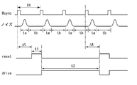
- FIG. 18A is a waveform diagram showing the relationship between the horizontal synchronization signal Hsync and the control signal in the area AR1.
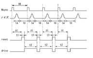
- FIG. 18B is a waveform diagram showing the relationship between the horizontal synchronization signal Hsync and the control signal in the area AR2.
- the touch panel 12 or the touch panel 13 may include a control unit 65 including a timing adjustment unit 63 instead of the control unit 60.
- the touch panel in which the sensor unit 30 is formed on the glass substrate has been described.
- the touch panel may be a film touch panel in which the sensor unit 30 is formed on a film.
- the display device with a touch panel 1 may include an organic EL (ElectroLuminescence) panel, a MEMS (Micro Electric Mechanical System) panel, or a plasma display panel instead of the liquid crystal display panel 20.
- organic EL ElectroLuminescence
- MEMS Micro Electric Mechanical System
- plasma display panel instead of the liquid crystal display panel 20.
- the present invention can be industrially used as a touch panel and a display device with a touch panel.
Landscapes
- Engineering & Computer Science (AREA)
- General Engineering & Computer Science (AREA)
- Theoretical Computer Science (AREA)
- Human Computer Interaction (AREA)
- Physics & Mathematics (AREA)
- General Physics & Mathematics (AREA)
- Position Input By Displaying (AREA)
Abstract
測定時間を短縮できるタッチパネルの構成を得る。タッチパネル(10)は、互いに交差する複数のドライブ電極(D1)~(Dm)および複数のセンサ電極(S1)~(Sn)を含むセンサ部(30)と、制御信号にしたがって、ドライブ期間において前記ドライブ電極(Di)と前記センサ電極(Sj)との交点の交点容量(Ci,j)を充電することによって前記交点容量(Ci,j)の静電容量を測定する測定部(40),(50)と、前記センサ部(30)を複数の領域に分割し、前記交点容量(Ci,j)のそれぞれが前記複数の領域のどの領域に属するかを判定する領域判定部と、前記領域判定部の判定結果に応じて前記ドライブ期間の長さが異なるように前記制御信号を生成する信号生成部とを備える。
Description
本発明は、タッチパネルおよびタッチパネル付き表示装置に関し、より詳しくは、静電容量方式のタッチパネルおよびタッチパネル付き表示装置に関する。
従来、タッチパネルと表示パネルとを重ねて配置することで、表示パネルを観察しながら操作ができるように構成されたタッチパネル付き表示装置が知られている。
特開2012-221423号公報には、あらかじめ用意された複数のパルス周期の中から一つのパルス周期を選択し、この選択されたパルス周期で出現する一連のパルスを含む同期信号(水平同期信号Hsync)を生成する信号生成部と、同期信号に基づき表示を行う表示部と、同期信号に基づきタッチ検出動作を行うタッチ検出部とを備えるタッチ検出機能付き表示パネルが記載されている。
タッチパネルの電極は、ITO(Indium Tin Oxide)等の透明導電膜によって形成される。ITOは金属と比較して電気抵抗が高いため、静電容量を精度よく測定するためには、静電容量の測定時間を長くする必要がある。そのため、タッチパネル全体の静電容量の測定にかかる時間も長くなり、応答性が低下する。一方、電極を金属にすることは、観察者に電極が視認されるため好ましくない。
本発明の目的は、タッチパネル全体の静電容量の測定にかかる時間を短縮できるタッチパネルの構成を得ることである。
ここに開示するタッチパネルは、互いに交差する複数のドライブ電極および複数のセンサ電極を含むセンサ部と、制御信号にしたがって、ドライブ期間において前記ドライブ電極と前記センサ電極との交点の交点容量を充電することによって前記交点容量の静電容量を測定する測定部と、前記センサ部を複数の領域に分割し、前記交点容量のそれぞれが前記複数の領域のどの領域に属するかを判定する領域判定部と、前記領域判定部の判定結果に応じて前記ドライブ期間の長さが異なるように前記制御信号を生成する信号生成部とを備える。
本発明によれば、タッチパネル全体の静電容量の測定にかかる時間を短縮できるタッチパネルの構成が得られる。
本発明の一実施形態にかかるタッチパネルは、互いに交差する複数のドライブ電極および複数のセンサ電極を含むセンサ部と、制御信号にしたがって、ドライブ期間において前記ドライブ電極と前記センサ電極との交点の交点容量を充電することによって前記交点容量の静電容量を測定する測定部と、前記センサ部を複数の領域に分割し、前記交点容量のそれぞれが前記複数の領域のどの領域に属するかを判定する領域判定部と、前記領域判定部の判定結果に応じて前記ドライブ期間の長さが異なるように前記制御信号を生成する信号生成部とを備える(第1の構成)。
上記の構成によれば、測定部は、交点容量を充電することによって交点容量の静電容量を測定する。交点容量を十分に充電するための時間は、交点容量の場所によって異なる。上記の構成によれば、領域判定部および信号生成部によって、交点容量の場所に応じて、充電時間を変えることができる。この構成によれば、すべての場所を同じ充電時間で測定する場合に比較して、タッチパネル全体の静電容量の測定にかかる時間を短縮することができる。
上記第1の構成において、前記信号生成部は、前記複数の領域のいずれか1つの領域におけるドライブ期間の長さを、当該領域に属する交点容量よりも時定数の大きい交点容量を含む他の領域における前記ドライブ期間の長さよりも短くしても良い(第2の構成)。
上記第1または第2の構成において、外部から同期信号を受け取り、前記同期信号を基準として前記制御信号を調整するタイミング調整部をさらに備えることが好ましい(第3の構成)。
上記の構成によれば、同期信号を基準として測定タイミングを調整することによって、特定の周期で発生するノイズを避けることができる。
上記第1~第3のいずれかの構成において、前記測定部は、前記制御信号にしたがって、リセット期間において前記交点容量を放電し、前記信号生成部は、前記領域判定部の判定結果に応じて前記リセット期間の長さが異なるように前記制御信号を生成することが好ましい(第4の構成)。
上記の構成によれば、交点容量ごとの測定時間をより適切に設定することができる。そのため、全体の測定時間をより短くすることができる。
上記第4の構成において、前記信号生成部は、前記複数の領域の1つでは前記リセット期間の長さと前記ドライブ期間の長さの和が1水平期間以下となるように前記制御信号を生成し、前記複数の領域の他の1つでは前記リセット期間の長さと前記ドライブ期間の長さの和が1水平期間より長くなるように前記制御信号を生成しても良い(第5の構成)。
上記第1~第5のいずれかの構成において、前記測定部は、前記交点容量を点順次で測定しても良い(第6の構成)。
上記の構成によれば、交点容量を測定する回路数を少なくできるので、消費電力を低減することができる。
上記第1~第5のいずれかの構成において、前記測定部は、前記交点容量を線順次で測定しても良い(第7の構成)。
上記の構成によれば、交点容量を並列に測定できるので、測定時間をより短くすることができる。
本発明の一実施形態にタッチパネル付き表示装置は、液晶表示パネルと、上記第1~第7のいずれかの構成のタッチパネルとを備える。
[実施の形態]
以下、図面を参照し、本発明の実施の形態を詳しく説明する。図中同一または相当部分には同一符号を付してその説明は繰り返さない。なお、説明を分かりやすくするために、以下で参照する図面においては、構成が簡略化または模式化して示されたり、一部の構成部材が省略されたりしている。また、各図に示された構成部材間の寸法比は、必ずしも実際の寸法比を示すものではない。
以下、図面を参照し、本発明の実施の形態を詳しく説明する。図中同一または相当部分には同一符号を付してその説明は繰り返さない。なお、説明を分かりやすくするために、以下で参照する図面においては、構成が簡略化または模式化して示されたり、一部の構成部材が省略されたりしている。また、各図に示された構成部材間の寸法比は、必ずしも実際の寸法比を示すものではない。
[第1の実施形態]
[全体の構成]
図1は、本発明の一実施形態にかかるタッチパネル付き表示装置1の概略構成を示す断面図である。タッチパネル付き表示装置1は、タッチパネル10と、液晶表示パネル20と、バックライトユニット25とを備えている。
[全体の構成]
図1は、本発明の一実施形態にかかるタッチパネル付き表示装置1の概略構成を示す断面図である。タッチパネル付き表示装置1は、タッチパネル10と、液晶表示パネル20と、バックライトユニット25とを備えている。
タッチパネル10は、液晶表示パネル20のバックライト25側と反対側の面に重ねて配置されている。タッチパネル10は、液晶表示装置20と、OCA(Optical Clear Adhesive)によって接着されている。
タッチパネル10は、詳しい構成は後述するが、強化ガラス製の基板と、この基板の一方の面に形成された電極群とを備えている。タッチパネル10は、電極群が形成された面が液晶表示パネル20側になるように配置されている。タッチパネル10の基板は、タッチパネル付き表示装置1のカバーガラスを兼ねている。すなわち、タッチパネル10は、カバーガラス一体型のタッチパネルである。
液晶表示パネル20は、TFT(Thin Film Transitor)基板21と、CF(Color Filter)基板22と、液晶23と、シール材24とを備えている。TFT基板21とCF基板22とは、互いに対向するように配置されている。TFT基板21とCF基板22とが向かい合う面の周縁部にはシール材24が形成されており、TFT基板21とCF基板22との間に液晶23が封入されている。
詳しい構成は図示していないが、TFT基板21は、複数の画素電極を備えている。液晶表示パネル20は、これらの画素電極の電位を制御することによって、液晶23の配向を制御する。これによって、液晶表示パネル20は、バックライトユニット25から照射される光の挙動を制御して階調を表現する。
[タッチパネル10の構成]
図2は、本発明の第1の実施形態にかかるタッチパネル10の機能的構成を示す機能ブロック図である。タッチパネル10は、センサ部30と、測定部(送信部40および受信部50)と、制御部60とを備えている。
図2は、本発明の第1の実施形態にかかるタッチパネル10の機能的構成を示す機能ブロック図である。タッチパネル10は、センサ部30と、測定部(送信部40および受信部50)と、制御部60とを備えている。
センサ部30は、m本のドライブ電極D1~Dmと、n本のセンサ電極S1~Snとを備えている(m、nは、正の整数)。ドライブ電極D1~Dmと、センサ電極S1~Snとは、互いに交差するように配置されている。これによって、ドライブ電極D1~Dmとセンサ電極S1~Snとの交点に、交点容量が形成される。以下、i番目のドライブ電極Di(iは1~mの整数)と、j番目のセンサ電極Sj(jは1~nの整数)との交点に形成される交点容量を、交点容量Ci,jと呼んで参照する。
交点容量Ci,jの静電容量は、センサ部30に指またはスタイラスペン等が接触または接近することによって変化する。そのため、交点容量Ci,jの静電容量を測定することによって、センサ部30に接触または接近した物体の座標を求めることができる。
制御部60は、測定部(送信部40および受信部50)を制御して、センサ部30の交点容量Ci,jの静電容量を測定する。
送信部40は、マルチプレクサ41と、駆動信号生成部42とを備えている。マルチプレクサ41は、ドライブ電極D1~Dmから1本の電極を選択し、駆動信号生成部42に接続する。駆動信号生成部42は、駆動信号を生成し、マルチプレクサ41によって選択された電極に供給する。
受信部50は、マルチプレクサ51と、電流電圧変換部(IVC(I/V Converter))52と、アナログ・ディジタル変換部(ADC(A/D Converter))53とを備えている。マルチプレクサ51は、センサ電極S1~Snから1本の電極を選択し、IVC52に接続する。IVC52は、マルチプレクサ51によって選択された電極から信号を受け取り、受け取った信号を電流から電圧に変換して、ADC53に供給する。ADC53は、受け取った信号をアナログ信号からディジタル信号に変換して、制御部60に供給する。
この構成によって、制御部60は、マルチプレクサ41によって選択された電極と、マルチプレクサ51によって選択された電極との交点の交点容量を測定することができる。制御部60は、すべてのドライブ電極D1~Dmと、すべてのセンサ電極センサ電極S1~Snとを走査して、n×m個の交点容量を測定する。
制御部60は、交点容量をドライブ電極ごとに測定する構成であっても良いし、交点容量をセンサ電極ごとに測定する構成であっても良い。すなわち、制御部60は、交点容量をC1,1~C1,n、C2,1~C2,n、・・・、Cm,1~Cm,nという順番で測定する構成であっても良いし、C1,1~Cm,1、C1,2~Cm,2、・・・、C1,n~Cm,nという順番で測定する構成であっても良い。あるいは、これらと異なる任意の順番で測定する構成であっても良い。
制御部60は、制御信号生成部61と、座標演算部62とを備えている。
制御信号生成部61は、送信部40および受信部50を制御するための制御信号を生成する。制御信号生成部61は、測定しようとする交点容量Ci,jの場所に応じて、異なる制御信号を生成する。制御信号生成部61の詳しい動作については後述する。
座標演算部62は、受信部50から交点容量Ci,jの静電容量に関連した値を受け取る。座標演算部62は、図示しない記憶装置を備え、受信部50から順次供給される値を記憶する。座標演算部62は、記憶装置に記憶された値の分布に基づいて所定の演算を行い、センサ部30に接触または接近した物体の座標を算出する。座標演算部62は、算出した座標を、タッチパネル10の外部に供給する。
次に、図3および図4を参照して、タッチパネル10の動作をより詳しく説明する。
図3は、タッチパネル10の構成の一部を抜き出して等価回路として示す図である。より具体的には、図3は、i番目のドライブ電極Diと、j番目のセンサ電極Sjと、これらに接続された回路とを抜き出して等価回路として示す図である。
図3に示すように、ドライブ電極Diは、多段接続されたRC回路として表すことができる。ここで、R1はドライブ電極Diと駆動信号生成回路42との間の配線の抵抗であり、C1は同配線の容量である。R2はドライブ電極Diの単位長さ当たりの抵抗であり、C2はドライブ電極Diの単位長さ当たりの寄生容量である。
同様に、センサ電極Sjは、多段接続されたRC回路として表すことができる。ここで、R3はセンサ電極Sjの単位長さ当たりの抵抗であり、C3はセンサ電極Sjの単位長さ当たりの寄生容量である。R4はセンサ電極SjとIVC52との間の配線の抵抗であり、C4は同配線の容量である。
駆動信号生成部42は、電源VDDと、切替スイッチ421とを備えている。切替スイッチ421は、制御部60から供給されるロジック信号driveに基づいて、マルチプレクサ41の接続先を電源VDDとグランド(GND)との間で切り替える。切替スイッチ421は、より具体的には、ロジック信号driveがハイレベルのときマルチプレクサ41を電源VDDに接続し、ロジック信号driveがローレベルのときマルチプレクサ41をGNDに接続する。
IVC52は、リセットスイッチ付きの積分回路である。すなわち、IVC52は、オペアンプ521と、積分容量Csと、リセットスイッチ522とを備えている。
オペアンプ521の反転入力端子は、センサ電極Sjと、積分容量Csの一方の電極とに並列に接続されている。オペアンプ521の非反転入力端子は、グランドに接続されている。オペアンプ521の出力端子は、積分容量Csの他方の電極と、ADC53とに並列に接続されている。
リセットスイッチ522は、積分容量Csの2つの電極に接続されている。リセットスイッチ522は、制御部60から供給されるロジック信号resetに基づいて開閉する。リセットスイッチ522は、より具体的には、ロジック信号resetがハイレベルのときオンになり、ロジック信号resetがローレベルのときオフになる。
制御信号生成部61は、領域判定部611と、信号生成部612とを備えている。領域判定部611は、センサ部30を2以上の領域に分割し、測定しようとしている交点容量Ci,jがどの領域に属しているかを判定する。領域判定部611は、判定結果を信号生成部612に供給する。信号生成部612は、領域判定部611の判定結果に基づいて、ロジック信号driveおよびロジック信号resetを含む制御信号を生成する。
図4は、タッチパネル10が交点容量Ci,jの静電容量を測定するときの信号波形図である。Vinは、駆動信号生成回路42からドライブ電極Diに供給される電圧である。Vcは、交点容量Ci,jに印加されている電圧である。Voutは、IVC52からADC53に出力される電圧である。
まず、リセット期間t1において、制御信号生成部61は、ロジック信号driveをローレベル(low)にし、ロジック信号resetをハイレベル(high)にする。これによって、VinはGNDになり、交点容量Ci,jが放電し、Vcが減少する。また、リセットスイッチ522がオンになり、積分容量Csが放電し、VoutがGNDになる。
次に、ドライブ期間t2において、制御信号生成部61は、ロジック信号driveをハイレベル(high)にし、ロジック信号resetをローレベル(low)にする。これによって、VinはVDDになり、交点容量Ci,jが充電され、Vcが増加する。このとき、IVC52に過渡電流が流れる。IVC52は、過渡電流を積分してVoutとして出力する。
制御部60は、ドライブ期間t2が終了する直前のVoutの値をサンプリングする。交点容量Ci,jが十分に長い時間充電されている場合、Voutは、次の式で表される。
Vout=-Ci,j×VDD/Cs
上式において、Csは積分容量Csの静電容量、Ci,jは交点容量Ci,jの静電容量である。VDDおよびCsの値は既知であるため、Voutを測定することによって、Ci,jを求めることができる。
Vout=-Ci,j×VDD/Cs
上式において、Csは積分容量Csの静電容量、Ci,jは交点容量Ci,jの静電容量である。VDDおよびCsの値は既知であるため、Voutを測定することによって、Ci,jを求めることができる。
交点容量Ci,jの静電容量を精度よく求めるため、リセット期間t1の長さを、交点容量Ci,jが十分に放電される時間に設定することが好ましい。また、ドライブ期間t2の長さを、交点容量Ci,jが十分に充電され、十分な過渡電流がIVC53に供給される時間に設定することが好ましい
一方、交点容量Ci,jが十分に充放電される時間、および十分な過渡電流がIVC53に供給される時間は、交点容量Ci,jの場所によって異なる。したがって、リセット期間t1およびドライブ期間t2の好ましい長さは、交点容量Ci,jの場所によって異なる。
すなわち、駆動信号生成部42から交点容量Ci,jまでの経路の長さ、および、駆動信号生成部42から交点容量Ci,jを経由してIVC52に到達する経路の長さは、交点容量Ci,jの場所によって異なる。図2に示す例では、交点容量C1,1を測定する場合の経路が最も長く、交点容量Cm,nを測定する場合の経路が最も短い。駆動信号生成部42から交点容量Ci,jまでの経路が長いほど、交点容量Ci,jの充放電に時間がかかる。また、駆動信号生成部42からIVC52までの経路が長いほど、交点容量Ci,jの測定に時間がかかる。
本実施形態にかかるタッチパネル10の構成によれば、リセット期間t1およびドライブ期間t2の長さを、交点容量Ci,jの場所に応じて変化させることができる。すなわち、制御信号生成部61の信号生成部612は、領域判定部611から供給される判定結果に応じて、リセット期間t1およびドライブ期間t2を異なる長さにする。
より詳しくは、信号生成部612は、複数の領域のいずれか1つの領域におけるドライブ期間t2の長さを、当該領域に属する交点容量よりも時定数の大きい交点容量を含む他の領域におけるドライブ期間t2の長さよりも短くする。また、信号生成部612は、信号生成部612は、複数の領域のいずれか1つの領域におけるリセット期間t1の長さを、当該領域に属する交点容量よりも時定数の大きい交点容量を含む他の領域におけるリセット期間t1の長さよりも短くする。
図5は、領域判定部611によるセンサ部30の分割の態様の一例を模式的に示す図である。図5の例では、領域判定部611は、センサ部30を、i≦pまたはj≦qである領域AR1と、p+1≦iかつq+1≦jである領域AR2とに分割している。ここで、pは1よりも大きくmよりも小さい整数であり、qは1よりも大きくnよりも小さい整数である。
領域AR1は、領域AR2に属するあらゆる交点容量よりも、時定数の大きい(充放電に時間がかかる)交点容量を含んでいる。すなわち、領域AR2に属する交点容量の中で、最も時定数の大きな交点容量はCp+1,q+1である。領域AR1は、これよりも時定数の大きい交点容量(例えば、C1,1)を含んでいる。
領域判定部611は、測定しようとしている交点容量Ci,jが、領域AR1に属するのか領域AR2に属するのかを判定し、判定結果を信号生成部612に供給する。信号生成部612は、領域AR1における制御信号のドライブ期間t2の長さを、領域AR2における制御信号のドライブ期間t2の長さよりも長くする。また、信号生成部612は、領域AR1における制御信号のリセット期間t1の長さを、領域AR2における制御信号のリセット期間t1の長さよりも長くする。
なお、リセット期間t1の長さは、ドライブ期間t2の長さと比較して短い。そのため、リセット期間t1の長さはすべての領域で一定にしておき、ドライブ期間t2の長さだけを領域に応じて変化させる構成にしても良い。
より好ましくは、信号生成部612は、領域AR1における制御信号のリセット期間t1およびドライブ期間t2の長さを、領域AR1に属する交点容量の中で送信部40および受信部50から最も遠い交点容量C1,1を十分に充放電できる長さにする。信号生成部612は、領域AR2における制御信号のリセット期間t1およびドライブ期間t2の長さを、領域AR2に属する交点容量の中で送信部40および受信部50から最も遠い交点容量Cp+1,q+1を十分に充放電できる長さにする。
これによって、すべての交点容量を同じ長さのリセット期間t1およびドライブ期間t2で測定する場合と比較して、全体の測定時間を短くすることができる。
図6は、領域判定部611によるセンサ部30の分割の態様の他の例を模式的に示す図である。図6の例では、領域判定部611は、センサ部30を、領域AR3と、領域AR4と、領域AR5とに分割している。
この場合、信号生成部612は、領域AR3におけるドライブ期間t2の長さ>領域AR4におけるドライブ期間t2の長さ>領域AR5におけるドライブ期間t2の長さ、となるように制御信号を生成する。また、信号生成部612は、領域AR3におけるリセット期間t1の長さ>領域AR4におけるリセット期間t1の長さ>領域AR5におけるリセット期間t1の長さ、となるように制御信号を生成する。
以上、本発明の第1の実施形態にかかるタッチパネル10について説明した。上記では、センサ部30を2つまた3つの領域に分割する例を説明した。しかし、センサ部30を、4つ以上の領域に分割し、それぞれの領域でリセット期間t1およびドライブ期間t2の長さが異なるようにしても良い。例えば、センサ部30を、m×nの領域に分割しても良い。すなわち、リセット期間t1およびドライブ期間t2の長さが、交点容量Ci,jごとにすべて異なるようにしても良い。
[第2の実施形態]
タッチパネル付き表示装置1は、タッチパネル10に代えて、以下に説明するタッチパネル11~13のいずれかを備えていても良い。
タッチパネル付き表示装置1は、タッチパネル10に代えて、以下に説明するタッチパネル11~13のいずれかを備えていても良い。
図7は、本発明の第2の実施形態にかかるタッチパネル11の機能的構成を示す機能ブロック図である。タッチパネル11は、制御部60に代えて、制御部65を備えている。制御部65は、制御部60の構成に加えて、タイミング調整部63をさらに備えている。
タイミング調整部63は、タッチパネル11の外部から同期信号を受け取る。より具体的には、タイミング調整部63は、液晶表示パネル20から、水平同期信号Hsyncを受け取る。タイミング調整部63は、水平同期信号Hsyncを基準として、制御信号生成部61が制御信号を生成するタイミングを調整する。
本実施形態においても、制御信号生成部61は、センサ部30を2以上の領域に分割し、測定しようとしている交点容量Ci,jが属する領域に応じて、リセット期間t1およびドライブ期間t2を異なる長さにする。
以下では一例として、センサ部30を図5に示す領域AR1と領域AR2とに分割する場合を考える。
図8Aは、水平同期信号Hsyncと、領域AR1における制御信号との関係を示す波形図である。図8Bは、水平同期信号Hsyncと、領域AR2における制御信号との関係を示す波形図である。
図8Aおよび図8Bにおける「ノイズ」は、液晶表示パネル20の動作に起因して発生するノイズレベルの高さを表している。このノイズは、例えば、液晶表示パネル20のソース書込みのタイミングで発生する。そのため、このノイズは、水平同期信号に対して所定のタイミングで発生する。1水平期間1Hの間には、比較的ノイズレベルが高いノイズ期間taと、比較的ノイズレベルが低い低ノイズ期間tbとが存在する。
タイミング調整部63は、リセット期間t1がノイズ期間taと重ならないように、制御信号生成部61の動作を調整する。より具体的には、リセット期間t1が開始するタイミングを、水平同期信号Hsyncの立ち上がりを基準として、所定時間Δtだけ遅延させる。
この構成によれば、液晶表示パネル20からのノイズの影響を低減し、より精度の高い測定を行うことができる。
制御信号生成部61は、領域AR1では、リセット期間t1の長さとドライブ期間t2との長さの和が3水平期間になるように制御信号を生成している。換言すれば、領域AR1では、制御部60は、3水平期間で1つの交点容量Ci,jを測定している。
制御信号生成部61は、領域AR2では、リセット期間t1の長さとドライブ期間t2との長さの和が1水平期間になるように制御信号を生成している。換言すれば、領域AR2では、制御部60は、1水平期間で1つの交点容量Ci,jを測定している。
この構成によれば、例えばすべての領域において3水平期間で1つの交点容量Ci,jを測定する構成と比較して、全体の測定時間を短くすることができる。あるいは、すべての領域において1水平期間で1つの交点容量Ci,jを測定する構成と比較して、領域AR1における測定精度を高くすることができる。
本実施形態においても、センサ部30をより多くの領域に分割して制御しても良い。また、リセット期間t1の長さとドライブ期間t2の長さとの和を1水平期間よりも短くできる領域では、1水平期間に複数の交点容量Ci,jを測定する構成としても良い。
[第3の実施形態]
図9は、本発明の第3の実施形態にかかるタッチパネル12の機能的構成を示す機能ブロック図である。タッチパネル12は、受信部50に代えて、受信部55を備えている。受信部55は、n個のIVC52と、n個のADC53とを備えている。
図9は、本発明の第3の実施形態にかかるタッチパネル12の機能的構成を示す機能ブロック図である。タッチパネル12は、受信部50に代えて、受信部55を備えている。受信部55は、n個のIVC52と、n個のADC53とを備えている。
受信部55は、この構成によって、n個の交点容量Ci,1~Ci,nを、並列に読み込むことができる。制御部60は、すべてのドライブ電極D1~Dmを走査して、n×m個の交点容量を測定する。
すなわち、タッチパネル12は、n×m個の交点容量を線順次で測定する。本実施形態によれば、n×m個の交点容量を点順次で測定するタッチパネル10と比較して、測定時間を1/nにすることができる。
本実施形態においても、制御信号生成部61は、センサ部30を2以上の領域に分割し、測定しようとしている交点容量Ci,jが属する領域に応じて、リセット期間t1およびドライブ期間t2を異なる長さにする。
図10は、領域判定部611によるセンサ部30の分割の態様の一例を模式的に示す図である。図10の例では、領域判定部611は、センサ部30を、i≦pである領域AR1と、p+1≦iである領域AR2とに分割している。ここで、pは1よりも大きくmよりも小さい整数である。
領域判定部611は、測定しようとしている交点容量Ci,jが、領域AR1に属するのか領域AR2に属するのかを判定し、判定結果を信号生成部612に供給する。信号生成部612は、領域AR1における制御信号のドライブ期間t2の長さを、領域AR2における制御信号のドライブ期間t2の長さよりも長くする。また、信号生成部612は、領域AR1における制御信号のリセット期間t1の長さを、領域AR2における制御信号のリセット期間t1の長さよりも長くする。
なお、i番目のドライブ電極Diから駆動信号を供給して交点容量Ci,1~Ci,nを読み込む場合、送信部40から最も遠い交点容量Ci,1を十分に充放電できるように、リセット時間t1およびドライブ時間t2を設定することが好ましい。の場合、ドライブ電極Diの整列方向において、iが大きい場所ほど(図9で右側に行くほど)受信部55との距離が短くなる。そのため、iが大きい場所ほど、リセット時間t1およびドライブ時間t2を短く設定することができる。
なお、制御部60は、ドライブ電極Diを、数ラインおきに駆動することが好ましい。例えば、ドライブ電極Diを3ラインおきに駆動する場合、D1、D4、・・・、Dm-2、D2、D5、・・・、Dm-1、D3、D6、・・・、Dmという順番で駆動する。これによって、タッチパネル12の応答性を良くすることができる。
なお、可能であれば1フレーム期間に複数回、すべての交点容量を読み込むことが好ましい。これによって、タッチパネル12の応答性を良くすることができる。例えば、1フレーム期間に4回、すべての交点容量を読み込むことが好ましい。
本実施形態においても、センサ部30をより多くの領域に分割して制御しても良い。例えば、センサ部30をmの領域に分割して制御しても良い。すなわち、リセット期間t1およびドライブ期間t2の長さが、ドライブ電極Diごとにすべて異なるようにしても良い。
[第4の実施形態]
図11は、本発明の第4の実施形態にかかるタッチパネル13の機能的構成を示す機能ブロック図である。タッチパネル13は、タッチパネル12と比較して、センサ部30の構成が異なっている。具体的には、タッチパネル12では、センサ電極Sjの一方の端部がIVC52に接続されているのに対し、タッチパネル13では、センサ電極Sjの両方の端部がIVC52に接続されている。
図11は、本発明の第4の実施形態にかかるタッチパネル13の機能的構成を示す機能ブロック図である。タッチパネル13は、タッチパネル12と比較して、センサ部30の構成が異なっている。具体的には、タッチパネル12では、センサ電極Sjの一方の端部がIVC52に接続されているのに対し、タッチパネル13では、センサ電極Sjの両方の端部がIVC52に接続されている。
この構成によれば、ドライブ電極Diの整列方向において、中央に近づくほど受信部52との距離が長くなり、両端に近づくほど受信部52との距離が短くなる。したがって、ドライブ電極Diの整列方向において、両端に近づくほど、リセット時間t1およびドライブ時間t2を短く設定することができる。
本実施形態によれば、第3の実施形態に比較して、全体の測定時間をより短くすることができる。
図12は、領域判定部611によるセンサ部30の分割の態様の一例を模式的に示す図である。図12の例では、領域判定部611は、センサ部30を、p+1≦i≦qである領域AR1と、i≦pである領域AR2と、q+1≦iである領域AR3に分割している。ここで、pおよびqは1<p<q<mの関係を満たす整数である。
領域判定部611は、測定しようとしている交点容量Ci,jが、領域AR1~領域AR3のどの領域に属するのかを判定し、判定結果を信号生成部612に供給する。信号生成部612は、領域AR1における制御信号のドライブ期間t2の長さを、領域AR2および領域AR3における制御信号のドライブ期間t2の長さよりも長くする。信号生成部612は、領域AR1における制御信号のリセット期間t1の長さを、領域AR2および領域AR3における制御信号のリセット期間t1の長さよりも長くする。
本実施形態においても、センサ部30をより多くの領域に分割して制御しても良い。
[タッチパネル付き表示装置の構成例]
以下、タッチパネル付き表示装置1の具体的な構成例を説明する。この構成例は、本発明を限定するものではない。
以下、タッチパネル付き表示装置1の具体的な構成例を説明する。この構成例は、本発明を限定するものではない。
図13は、タッチパネル10の具体的な構成の一例を示す平面図である。図14は、図13のXIV-XIV線に沿った断面図である。
タッチパネル10は、基板300と、複数の透明電極31および32と、絶縁膜33と、保護膜34とを備えている。この例では、透明電極31がドライブ電極D1~Dmに相当し、透明電極32がドライブ電極D1~Dmに相当する。
基板300は、例えば強化ガラスである。基板300は、既述のように、タッチパネル付き表示装置1のカバーガラスを兼ねている。
透明電極31および32は、例えばITOの膜である。絶縁膜33は、例えば窒化ケイ素の膜である。保護膜34は、例えばアクリル樹脂である。保護膜34は、透明電極31および32、ならびに絶縁膜33を覆って形成されている。
透明電極31のそれぞれは、概略矩形の島状部311と、隣接する島状部311同士を接続する接続部312とを含んでいる。同様に、透明電極32のそれぞれは、概略矩形の島状部321と、隣接する島状部321同士を接続する接続部322とを含んでいる。
透明電極31の島状部311および接続部312、ならびに透明電極32の島状部321は、基板11上に形成され、絶縁膜33に覆われている。透明電極32の接続部322は、絶縁部33上に形成されている。透明電極32の島状部321と接続部322とは、絶縁膜33に形成されたコンタクトホール33aを介して接続している。
すなわち、透明電極31と透明電極32とは、絶縁膜33を間に挟んで交差している。この構成によって、透明電極31と透明電極32との交点に、交点容量Ci,jが形成される。
図15は、タッチパネル10の具体的な構成の他の例を示す分解斜視図である。図16は、図15のXVI-XVI線に沿った断面図である。
タッチパネル10は、基板301と、複数の透明電極34および35と、保護膜36および37と、カバーガラス302とを備えている。この例では、透明電極34がドライブ電極D1~Dmに相当し、透明電極35がセンサ電極S1~Snに相当する。
基板301は、例えばガラス基板である。透明電極34および35は、例えばITOである。保護膜36および37は、例えばアクリル樹脂である。保護膜36は、透明電極34を覆って形成されている。保護膜37は、透明電極35を覆って形成されている。
カバーガラス302は、例えば強化ガラスである。カバーガラス302は、保護膜37とOCAによって接着されている。
透明電極34と透明電極35とは、平面視で互いに交差するように形成されている。透明電極34は基板301の一方の面に形成され、透明電極35は基板301の他方の面に形成されている。
すなわち、透明電極34と透明電極35とは、基板301を間に挟んで交差している。この構成によって、透明電極34と透明電極35との交点に、交点容量Ci,jが形成される。
次に、図3を参照して、第2の実施形態にかかるタッチパネル11の交点容量Ci,jを測定するときの各回路の時定数を具体的に計算する。タッチパネル11は、14.2型のタッチパネルであり、m=55本のドライブ電極と、n=73本のセンサ電極とを備えているものとする。
ここで、配線の抵抗R1=R4=500Ω、配線の容量C1=C4=19pFとする。電極の単位長さ当たりの抵抗(ドライブ電極Diとセンサ電極Sjと交点から、次の交点までの間の抵抗)R2=R3=120Ω、電極の単位長さ当たりの規制容量(ドライブ電極Diとセンサ電極Sjと交点から、次の交点までの間の規制容量)C2=C3=12.7pFとする。交点容量Ci,j=1.22pFとする。
駆動信号生成回路42およびIVC52から最も遠い交点容量を測定する場合、すなわち交点容量C1,1を測定する場合、駆動信号生成回路42と交点容量C1,1の間の時定数は、約2.00μsである。また、駆動信号生成回路42とIVC52との間の時定数は、約6.28μsである。
一方、駆動信号生成回路42およびIVC52から最も近い交点容量を測定する場合、すなわち交点容量C55,73を測定する場合、駆動信号生成回路42と交点容量C55,73の間の時定数は、約0.013μsである。また、駆動信号生成回路42とIVC52との間の時定数は、約0.054μsである。
このように、時定数は測定しようとする交点容量の場所によって大きく異なる。
リセット時間t1およびドライブ時間t2の長さを、時定数の2.75倍(交点容量C1,1が約93.6%充電される時間)に設定する場合、交点容量C1,1を測定するときは、リセット時間t1は5.50μs、ドライブ時間t2は17.26μsになる。なお、交点容量Cm,nを測定するときは、リセット時間t1は0.036μs、ドライブ時間t2は0.148μsになる。
液晶表示パネル20の表示解像度を2560×1920、フレームレートを60fpsとすると、1水平期間1Hの長さは約8.6μsである。したがって、交点容量C1,1を上記の条件で測定するためには3水平期間が必要である。
ここで、センサパネル30を、図17の様に領域AR1と領域AR2とに分割する。すなわち、i≦24またはj≦32である領域AR1と、i≧25かつj≧33である領域AR2とに分割する。領域AR2に属する交点容量の中で送信部40および受信部50から最も遠い交点容量C25,33を上記の条件で測定する場合、リセット時間t1は1.85μs、ドライブ時間t2は5.87μsとなる。リセット時間t1+ドライブ時間t2=7.72μsとなり、1水平期間内に収まる
図18Aは、水平同期信号Hsyncと、領域AR1における制御信号との関係を示す波形図である。図18Bは、水平同期信号Hsyncと、領域AR2における制御信号との関係を示す波形図である。
この構成例によれば、センサ部30全体を、{(55×73)-(30×40)}×3+(30×40)×1=9645水平期間で測定する。これに対し、すべての領域において3水平期間で1つの交点容量Ci,jを測定する場合、センサ部30全体を(55×73)×3=12045水平期間で測定する。このように、本実施形態によれば、全体の測定時間を短くすることができる。
[その他の実施形態]
以上、本発明についての実施形態を説明したが、本発明は上述の各実施形態のみに限定されず、発明の範囲内で種々の変更が可能である。また、各実施形態は、適宜組み合わせて実施することが可能である。
以上、本発明についての実施形態を説明したが、本発明は上述の各実施形態のみに限定されず、発明の範囲内で種々の変更が可能である。また、各実施形態は、適宜組み合わせて実施することが可能である。
例えば、タッチパネル12またはタッチパネル13は、制御部60に代えて、タイミング調整部63を含んだ制御部65を備えていても良い。
上述の実施形態では、ガラス基板にセンサ部30が形成されたタッチパネルの構成を説明したが、タッチパネルは、フィルムの上にセンサ部30が形成された、フィルムタッチパネルであっても良い。
タッチパネル付き表示装置1は、液晶表示パネル20に代えて、有機EL(ElectroLuminescence)パネルや、MEMS(Micro Electric Mechanical System)パネル、プラズマ表示パネルを備えていても良い。
本発明は、タッチパネルおよびタッチパネル付き表示装置として産業上の利用が可能である。
Claims (8)
- 互いに交差する複数のドライブ電極および複数のセンサ電極を含むセンサ部と、
制御信号にしたがって、ドライブ期間において前記ドライブ電極と前記センサ電極との交点の交点容量を充電することによって前記交点容量の静電容量を測定する測定部と、
前記センサ部を複数の領域に分割し、前記交点容量のそれぞれが前記複数の領域のどの領域に属するかを判定する領域判定部と、
前記領域判定部の判定結果に応じて前記ドライブ期間の長さが異なるように前記制御信号を生成する信号生成部とを備える、タッチパネル。 - 前記信号生成部は、前記複数の領域のいずれか1つの領域におけるドライブ期間の長さを、当該領域に属する交点容量よりも時定数の大きい交点容量を含む他の領域におけるドライブ期間の長さよりも短くする、請求項1に記載のタッチパネル。
- 外部から同期信号を受け取り、前記同期信号を基準として前記制御信号を調整するタイミング調整部をさらに備える、請求項1または2に記載のタッチパネル。
- 前記測定部は、前記制御信号にしたがって、リセット期間において前記交点容量を放電し、
前記信号生成部は、前記領域判定部の判定結果に応じて前記リセット期間の長さが異なるように前記制御信号を生成する、請求項1~3のいずれか一項に記載のタッチパネル。 - 前記信号生成部は、前記複数の領域の1つでは前記リセット期間の長さと前記ドライブ期間の長さの和が1水平期間以下となるように前記制御信号を生成し、前記複数の領域の他の1つでは前記リセット期間の長さと前記ドライブ期間の長さの和が1水平期間より長くなるように前記制御信号を生成する、請求項4に記載のタッチパネル。
- 前記測定部は、前記交点容量を点順次で測定する、請求項1~5のいずれか一項に記載のタッチパネル。
- 前記測定部は、前記交点容量を線順次で測定する、請求項1~5のいずれか一項に記載のタッチパネル。
- 液晶表示パネルと、
請求項1~7のいずれか一項に記載のタッチパネルとを備えるタッチパネル付き表示装置。
Priority Applications (1)
| Application Number | Priority Date | Filing Date | Title |
|---|---|---|---|
| US14/785,053 US20160085337A1 (en) | 2013-04-24 | 2014-02-25 | Touch panel and display device with touch panel |
Applications Claiming Priority (2)
| Application Number | Priority Date | Filing Date | Title |
|---|---|---|---|
| JP2013-091669 | 2013-04-24 | ||
| JP2013091669 | 2013-04-24 |
Publications (1)
| Publication Number | Publication Date |
|---|---|
| WO2014174886A1 true WO2014174886A1 (ja) | 2014-10-30 |
Family
ID=51791471
Family Applications (1)
| Application Number | Title | Priority Date | Filing Date |
|---|---|---|---|
| PCT/JP2014/054451 Ceased WO2014174886A1 (ja) | 2013-04-24 | 2014-02-25 | タッチパネルおよびタッチパネル付き表示装置 |
Country Status (2)
| Country | Link |
|---|---|
| US (1) | US20160085337A1 (ja) |
| WO (1) | WO2014174886A1 (ja) |
Families Citing this family (1)
| Publication number | Priority date | Publication date | Assignee | Title |
|---|---|---|---|---|
| JP5616557B1 (ja) * | 2013-08-08 | 2014-10-29 | パナソニック インテレクチュアル プロパティ コーポレーション オブアメリカPanasonic Intellectual Property Corporation of America | 電子機器および座標検出方法 |
Citations (2)
| Publication number | Priority date | Publication date | Assignee | Title |
|---|---|---|---|---|
| JP2010073150A (ja) * | 2008-09-22 | 2010-04-02 | Sony Corp | 静電容量型センサーデバイスの容量変化検出回路、静電容量型センサーモジュール、静電容量型センサーデバイスの容量変化検出方法及び電子機器 |
| JP2011238146A (ja) * | 2010-05-13 | 2011-11-24 | Mitsubishi Electric Corp | タッチパネルおよびそれを備える表示装置 |
Family Cites Families (4)
| Publication number | Priority date | Publication date | Assignee | Title |
|---|---|---|---|---|
| US8564547B2 (en) * | 2008-04-15 | 2013-10-22 | Mattel, Inc. | Touch screen remote control device for use with a toy |
| US8659557B2 (en) * | 2008-10-21 | 2014-02-25 | Atmel Corporation | Touch finding method and apparatus |
| WO2011145677A1 (ja) * | 2010-05-20 | 2011-11-24 | シャープ株式会社 | タッチセンサ付き表示装置 |
| US20130265242A1 (en) * | 2012-04-09 | 2013-10-10 | Peter W. Richards | Touch sensor common mode noise recovery |
-
2014
- 2014-02-25 US US14/785,053 patent/US20160085337A1/en not_active Abandoned
- 2014-02-25 WO PCT/JP2014/054451 patent/WO2014174886A1/ja not_active Ceased
Patent Citations (2)
| Publication number | Priority date | Publication date | Assignee | Title |
|---|---|---|---|---|
| JP2010073150A (ja) * | 2008-09-22 | 2010-04-02 | Sony Corp | 静電容量型センサーデバイスの容量変化検出回路、静電容量型センサーモジュール、静電容量型センサーデバイスの容量変化検出方法及び電子機器 |
| JP2011238146A (ja) * | 2010-05-13 | 2011-11-24 | Mitsubishi Electric Corp | タッチパネルおよびそれを備える表示装置 |
Non-Patent Citations (1)
| Title |
|---|
| SEUNGHOON KO ET AL.: "Low noise capacitive sensor for multi-touch mobile handset's applications", SOLID STATE CIRCUITS CONFERENCE (A-SSCC), 2010 IEEE ASIAN, BEIJING, pages 1 - 4 * |
Also Published As
| Publication number | Publication date |
|---|---|
| US20160085337A1 (en) | 2016-03-24 |
Similar Documents
| Publication | Publication Date | Title |
|---|---|---|
| CN103809801B (zh) | 包括集成式触摸面板的显示装置 | |
| JP6665051B2 (ja) | 表示装置及びその駆動方法 | |
| US8174273B2 (en) | Capacitance measurement circuit with dynamic feedback | |
| KR101658910B1 (ko) | 기생 커패시턴스의 영향을 감소시키는 터치입력 감지방법 및 이를 위한 장치 | |
| KR101886255B1 (ko) | 드라이빙 백 현상을 이용한 터치 검출수단, 검출방법 및 터치스크린패널과, 그러한 터치스크린패널을 내장한 표시장치 | |
| US8599146B2 (en) | Liquid crystal device, electronic apparatus and position identification method for identifying a position of an object | |
| KR102177540B1 (ko) | 터치 스크린 일체형 표시장치 및 그 구동 방법 | |
| KR102117342B1 (ko) | 터치 스크린 일체형 표시장치 및 그 구동 방법 | |
| KR102412369B1 (ko) | 터치 스크린 일체형 표시 장치 | |
| CN102859471B (zh) | 带触摸传感器的显示装置 | |
| KR101566939B1 (ko) | 정전식 터치 신호 검출 장치 및 방법 | |
| US20140375609A1 (en) | Apparatus and method for detecting touch, capable of reducing parasitic capacitance | |
| WO2011125521A1 (ja) | タッチセンサ付き表示装置 | |
| KR102333962B1 (ko) | 터치 감지 장치 및 그를 포함하는 터치 표시 장치 | |
| WO2014174886A1 (ja) | タッチパネルおよびタッチパネル付き表示装置 | |
| KR101695231B1 (ko) | 드라이빙 백 현상을 이용한 터치 검출수단 | |
| KR101678060B1 (ko) | 저주파 노이즈를 제거하는 터치입력장치 | |
| TW201426478A (zh) | 電容式觸控裝置及其觸控感測方法 | |
| KR20140124256A (ko) | 터치스크린 장치 및 터치패널 구동방법 | |
| KR20140148360A (ko) | 드라이빙 백 현상을 이용한 터치 검출수단, 검출방법 및 터치스크린패널과, 그러한 터치스크린패널을 내장한 표시장치 |
Legal Events
| Date | Code | Title | Description |
|---|---|---|---|
| 121 | Ep: the epo has been informed by wipo that ep was designated in this application |
Ref document number: 14788292 Country of ref document: EP Kind code of ref document: A1 |
|
| WWE | Wipo information: entry into national phase |
Ref document number: 14785053 Country of ref document: US |
|
| NENP | Non-entry into the national phase |
Ref country code: DE |
|
| 122 | Ep: pct application non-entry in european phase |
Ref document number: 14788292 Country of ref document: EP Kind code of ref document: A1 |
|
| NENP | Non-entry into the national phase |
Ref country code: JP |