WO2014156712A1 - 複眼光学系及び撮像装置 - Google Patents
複眼光学系及び撮像装置 Download PDFInfo
- Publication number
- WO2014156712A1 WO2014156712A1 PCT/JP2014/056851 JP2014056851W WO2014156712A1 WO 2014156712 A1 WO2014156712 A1 WO 2014156712A1 JP 2014056851 W JP2014056851 W JP 2014056851W WO 2014156712 A1 WO2014156712 A1 WO 2014156712A1
- Authority
- WO
- WIPO (PCT)
- Prior art keywords
- lens
- optical system
- compound
- imaging
- image
- Prior art date
- Legal status (The legal status is an assumption and is not a legal conclusion. Google has not performed a legal analysis and makes no representation as to the accuracy of the status listed.)
- Ceased
Links
Images


Classifications
-
- G—PHYSICS
- G02—OPTICS
- G02B—OPTICAL ELEMENTS, SYSTEMS OR APPARATUS
- G02B3/00—Simple or compound lenses
- G02B3/0006—Arrays
- G02B3/0037—Arrays characterized by the distribution or form of lenses
- G02B3/0043—Inhomogeneous or irregular arrays, e.g. varying shape, size, height
-
- G—PHYSICS
- G02—OPTICS
- G02B—OPTICAL ELEMENTS, SYSTEMS OR APPARATUS
- G02B13/00—Optical objectives specially designed for the purposes specified below
- G02B13/001—Miniaturised objectives for electronic devices, e.g. portable telephones, webcams, PDAs, small digital cameras
- G02B13/0015—Miniaturised objectives for electronic devices, e.g. portable telephones, webcams, PDAs, small digital cameras characterised by the lens design
- G02B13/005—Miniaturised objectives for electronic devices, e.g. portable telephones, webcams, PDAs, small digital cameras characterised by the lens design having spherical lenses only
-
- G—PHYSICS
- G02—OPTICS
- G02B—OPTICAL ELEMENTS, SYSTEMS OR APPARATUS
- G02B27/00—Optical systems or apparatus not provided for by any of the groups G02B1/00 - G02B26/00, G02B30/00
- G02B27/0025—Optical systems or apparatus not provided for by any of the groups G02B1/00 - G02B26/00, G02B30/00 for optical correction, e.g. distorsion, aberration
-
- G—PHYSICS
- G02—OPTICS
- G02B—OPTICAL ELEMENTS, SYSTEMS OR APPARATUS
- G02B27/00—Optical systems or apparatus not provided for by any of the groups G02B1/00 - G02B26/00, G02B30/00
- G02B27/10—Beam splitting or combining systems
- G02B27/1066—Beam splitting or combining systems for enhancing image performance, like resolution, pixel numbers, dual magnifications or dynamic range, by tiling, slicing or overlapping fields of view
-
- G—PHYSICS
- G02—OPTICS
- G02B—OPTICAL ELEMENTS, SYSTEMS OR APPARATUS
- G02B27/00—Optical systems or apparatus not provided for by any of the groups G02B1/00 - G02B26/00, G02B30/00
- G02B27/10—Beam splitting or combining systems
- G02B27/12—Beam splitting or combining systems operating by refraction only
- G02B27/123—The splitting element being a lens or a system of lenses, including arrays and surfaces with refractive power
-
- G—PHYSICS
- G02—OPTICS
- G02B—OPTICAL ELEMENTS, SYSTEMS OR APPARATUS
- G02B3/00—Simple or compound lenses
- G02B3/0006—Arrays
- G02B3/0037—Arrays characterized by the distribution or form of lenses
- G02B3/0056—Arrays characterized by the distribution or form of lenses arranged along two different directions in a plane, e.g. honeycomb arrangement of lenses
-
- G—PHYSICS
- G02—OPTICS
- G02B—OPTICAL ELEMENTS, SYSTEMS OR APPARATUS
- G02B3/00—Simple or compound lenses
- G02B3/0006—Arrays
- G02B3/0037—Arrays characterized by the distribution or form of lenses
- G02B3/0062—Stacked lens arrays, i.e. refractive surfaces arranged in at least two planes, without structurally separate optical elements in-between
-
- G—PHYSICS
- G06—COMPUTING OR CALCULATING; COUNTING
- G06T—IMAGE DATA PROCESSING OR GENERATION, IN GENERAL
- G06T5/00—Image enhancement or restoration
- G06T5/50—Image enhancement or restoration using two or more images, e.g. averaging or subtraction
-
- H—ELECTRICITY
- H04—ELECTRIC COMMUNICATION TECHNIQUE
- H04N—PICTORIAL COMMUNICATION, e.g. TELEVISION
- H04N23/00—Cameras or camera modules comprising electronic image sensors; Control thereof
- H04N23/60—Control of cameras or camera modules
- H04N23/698—Control of cameras or camera modules for achieving an enlarged field of view, e.g. panoramic image capture
-
- H—ELECTRICITY
- H04—ELECTRIC COMMUNICATION TECHNIQUE
- H04N—PICTORIAL COMMUNICATION, e.g. TELEVISION
- H04N25/00—Circuitry of solid-state image sensors [SSIS]; Control thereof
- H04N25/60—Noise processing, e.g. detecting, correcting, reducing or removing noise
- H04N25/61—Noise processing, e.g. detecting, correcting, reducing or removing noise the noise originating only from the lens unit, e.g. flare, shading, vignetting or "cos4"
-
- H—ELECTRICITY
- H10—SEMICONDUCTOR DEVICES; ELECTRIC SOLID-STATE DEVICES NOT OTHERWISE PROVIDED FOR
- H10F—INORGANIC SEMICONDUCTOR DEVICES SENSITIVE TO INFRARED RADIATION, LIGHT, ELECTROMAGNETIC RADIATION OF SHORTER WAVELENGTH OR CORPUSCULAR RADIATION
- H10F39/00—Integrated devices, or assemblies of multiple devices, comprising at least one element covered by group H10F30/00, e.g. radiation detectors comprising photodiode arrays
- H10F39/80—Constructional details of image sensors
- H10F39/806—Optical elements or arrangements associated with the image sensors
-
- H—ELECTRICITY
- H10—SEMICONDUCTOR DEVICES; ELECTRIC SOLID-STATE DEVICES NOT OTHERWISE PROVIDED FOR
- H10F—INORGANIC SEMICONDUCTOR DEVICES SENSITIVE TO INFRARED RADIATION, LIGHT, ELECTROMAGNETIC RADIATION OF SHORTER WAVELENGTH OR CORPUSCULAR RADIATION
- H10F39/00—Integrated devices, or assemblies of multiple devices, comprising at least one element covered by group H10F30/00, e.g. radiation detectors comprising photodiode arrays
- H10F39/80—Constructional details of image sensors
- H10F39/806—Optical elements or arrangements associated with the image sensors
- H10F39/8063—Microlenses
-
- G—PHYSICS
- G02—OPTICS
- G02B—OPTICAL ELEMENTS, SYSTEMS OR APPARATUS
- G02B27/00—Optical systems or apparatus not provided for by any of the groups G02B1/00 - G02B26/00, G02B30/00
- G02B27/02—Viewing or reading apparatus
- G02B27/022—Viewing apparatus
- G02B27/024—Viewing apparatus comprising a light source, e.g. for viewing photographic slides, X-ray transparancies
- G02B27/025—Viewing apparatus comprising a light source, e.g. for viewing photographic slides, X-ray transparancies and magnifying means
-
- G—PHYSICS
- G06—COMPUTING OR CALCULATING; COUNTING
- G06T—IMAGE DATA PROCESSING OR GENERATION, IN GENERAL
- G06T2207/00—Indexing scheme for image analysis or image enhancement
- G06T2207/20—Special algorithmic details
- G06T2207/20212—Image combination
Definitions
- the present invention relates to an image pickup apparatus having an image processing unit that is formed on one solid-state image pickup device and outputs one image by joining images of different fields of view, and a compound eye optical system used therefor.
- a compound-eye optical system that divides the imaging region of the imaging device, disposes lenses (hereinafter referred to as single-lens lenses), and processes the obtained images, thereby outputting a final image.
- a so-called optical system has attracted attention in order to meet the demand for thinning (see Patent Document 1).
- FIG. 1B shows a comparison between the MTF values at the axial best imaging position and the position shifted by D from the best imaging position on the axis.
- the optical system A on the peripheral side has a larger curvature of field (D B ⁇ D A ) and the image forming performance tends to deteriorate (out of focus) than the optical system B on the central side. Become.
- the lens surface (or lens group) of the single-lens lens arranged in the periphery is decentered and curved.
- the image plane being tilted is tilted so as to create a state in focus within the use photographing range (see Patent Document 1).
- the focus position is improved.
- the optical axis of the lens is tilted so that the best imaging position on the axis of the single lens is brought closer.
- the tendency of the imaging performance to deteriorate as the single-lens lens arranged in the periphery does not change.
- the present invention has been made in view of the problems of the prior art, and can solve the problem of aberration in the field division type optical system to obtain a high-quality image, and is an ultra-thin imaging device.
- An object of the present invention is to provide a compound eye optical system capable of achieving the above and an imaging apparatus using the same.
- a compound-eye optical system is a compound-eye optical system used on an image pickup apparatus having an image processing unit that is formed on one solid-state image pickup device and that combines images of different fields of view and outputs one image.
- An array lens including a plurality of lenses formed integrally with at least one and having different optical axes;
- a plurality of single-lens lenses that form an image corresponding to each field of view are composed of lenses of the array lens, At least one of Formula (1) or Formula (2) is established.
- ⁇ h_d Horizontal shooting range of the peripheral single lens arranged on the peripheral side of the central single lens of the array lens
- the maximum shooting angle in the horizontal direction incident on the single lens is ⁇ h_max
- the minimum shooting angle is ⁇ h_min
- the maximum shooting angle in the vertical direction is ⁇ v_max
- the imaging performance of the peripheral single-lens lens tends to deteriorate with respect to the central single-lens lens.
- the amount of curvature of field in the shooting range can be reduced, so the amount of eccentricity of the lens surface (or lens group) can be reduced. It can be reduced.
- the shooting range of the single lens arranged near the periphery is narrowed on the condition that the shooting range of the compound eye optical system is not changed, the shooting range of the single lens arranged near the center needs to be widened. Since the lens located near the center has a relatively wide imaging performance compared to the lenses near the periphery, even if the shooting range is somewhat widened, degradation of the imaging performance is not a big problem. .
- An imaging apparatus includes the compound eye optical system, a solid-state imaging device, and an image processing unit.
- a compound-eye optical system capable of solving the problem of aberration in a field division type optical system and obtaining a high-quality image and achieving an ultra-thin imaging device, and imaging using the same An apparatus can be provided.
- (A) (b) is a figure for demonstrating curvature of field. It is a figure for demonstrating the curvature of field in the optical system of a visual field division
- (A) (b) is a figure explaining tilting a lens and correcting field distortion. It is a figure which shows typically the imaging device concerning this Embodiment. It is sectional drawing of a compound eye optical system.
- (A) (b) is a top view for demonstrating the positional relationship of a compound-eye optical system and an imaging region.
- (a) is a schematic diagram which shows the imaging range of a comparative example
- (b) is a schematic diagram which shows the imaging range of an Example
- (c) is a top view which shows arrangement
- (A), (b), (c), and (d) are graphs showing the MTF values in the imaging ranges D1, V1, H1, and C of the comparative example.
- (A), (b), (c), and (d) are graphs of MTF values in the imaging ranges D1, V1, H1, and C of the embodiment.
- a compound eye optical system is an optical system in which a plurality of lens systems are arranged in an array for one image sensor, and each lens system has a different field of view and a super-resolution type in which each lens system images the same field of view. Usually, it is divided into a field division type that performs imaging of the above.
- the compound eye optical system according to the present invention corresponds to a field division type in which a plurality of images with different fields of view are formed in order to connect a plurality of images with different fields of view and output a single composite image.
- FIG. 4 schematically illustrates the imaging apparatus according to the present embodiment
- FIG. 5 illustrates a cross-sectional view of the compound eye optical system according to the present embodiment
- FIG. 6 illustrates the positional relationship between the compound eye optical system and the imaging region.
- the imaging device DU includes an imaging unit LU, an image processing unit 1, a calculation unit 2, a memory 3, and the like.
- the imaging unit LU includes one imaging element SR and a compound-eye optical system LH that performs a plurality of imaging with different fields of view on the imaging element SR.
- the image sensor SR for example, a solid-state image sensor such as a CCD image sensor or a CMOS image sensor having a plurality of pixels is used.
- the compound eye optical system LH is provided on the light receiving surface SS which is a photoelectric conversion unit of the image sensor SR so that an optical image of the subject is formed, the optical image formed by the compound eye optical system LH is captured. It is converted into an electrical signal by the element SR.
- the cover glass CG of the image sensor SR is arranged on the image side of the second lens array LA2, and only the imaging light from each individual lens Ln is transmitted through the image side surface thereof.
- a light shielding member AP having a plurality of openings formed therein is disposed.
- a plurality of images having different fields of view are captured on the imaging surface SS (for example, solid-state imaging) of one imaging element SR.
- a plurality of single-lens lenses are formed on the photoelectric conversion portion of the element.
- FIG. 6B a part (L13 to L15, L18 to L20, L23) of the individual lens Ln that forms the individual image Zn (FIGS. 4 and 5) in the individual eye region Pn (FIG. 6A). To L25).
- the circular shape in FIG.6 (b) has shown the state (for example, elliptical shape is the eccentric state of a lens system) which looked at the single lens Ln from the upper direction.
- FIG. 5 corresponds to a cross-sectional view taken along the line QQ ′ of FIG. 6B (one cross section in the V direction), but the single lens Ln is arranged symmetrically in the vertical and horizontal directions. ) Shows only the single lens Ln of 9 positions (L13 to L15, L18 to L20, L23 to L25).
- the first embodiment is configured to perform 5 ⁇ 5 field division, as can be seen from FIG. 6, the single lens Ln and the single eye region Pn are in a corresponding array of 5 ⁇ 5. .
- the magnification of each individual lens Ln is substantially equal.
- the central single lens (center single lens) L13 forms an image of the subject center, and the peripheral single lens Ln (other than L13: peripheral single lens) forms an image around the subject.
- the angle of view of any single lens Ln is narrow.
- the horizontal shooting range of the central single lens is ⁇ h_c
- the vertical shooting range of the central single lens DL1 is ⁇ v_c
- the horizontal shooting range of the peripheral single lens is ⁇ h_d
- the vertical single lens DL2 is vertical.
- the single lens Ln has a two-lens configuration, and has a central single lens L13 (optical axis AX perpendicular to the imaging surface SS) shown in FIG. Is a positive and negative telephoto type power arrangement.
- the peripheral single lens Ln other than the central single lens L13 has four free-form surfaces. With the configuration having four free-form surfaces, very good aberration performance can be realized. Since the single lens Ln other than the central single lens L13 has a decentered optical axis AX in order to form a peripheral visual field, it is not necessary to use an optical path changing prism or the like. Therefore, all the monocular lenses Ln can have the same thickness and can be designed on the same substrate.
- the single lens Ln constituting the peripheral visual field makes light incident obliquely with respect to the imaging surface SS. Therefore, at least two lenses are necessary to ensure optical performance, and the same optical system as the axially symmetric optical system is used. In order to obtain performance, it is preferable to have four free-form surfaces.
- a light shielding member AP is disposed between the lens array LA2 and the imaging surface so that the imaging surface for each single-lens lens can be used appropriately in accordance with the imaging range.
- crosstalk occurs
- the light shielding member AP suppresses the crosstalk. It is desirable to insert a light shielding member not only between the single lens and the imaging surface but also between the lens arrays so that crosstalk does not occur as much as possible.
- the image processing unit 1 includes an image composition unit 1a, an image correction unit 1b, and an output image processing unit 1c.
- the eye composite image ML is output.
- the image correction unit 1b performs inversion processing, distortion processing, shading processing, stitching processing, and the like. Further, distortion correction is performed as necessary.
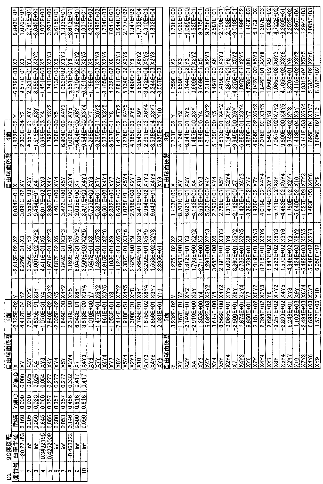
- Example 5 an example suitable for the compound eye optical system described above will be described in more detail while comparing with comparative examples using construction data and the like.
- the examples given here are numerical examples corresponding to the above-described embodiments, and an optical configuration diagram (FIG. 5) showing an embodiment of the compound-eye optical system LH is a lens configuration, an optical path, and the like of the corresponding numerical examples. Is shown.
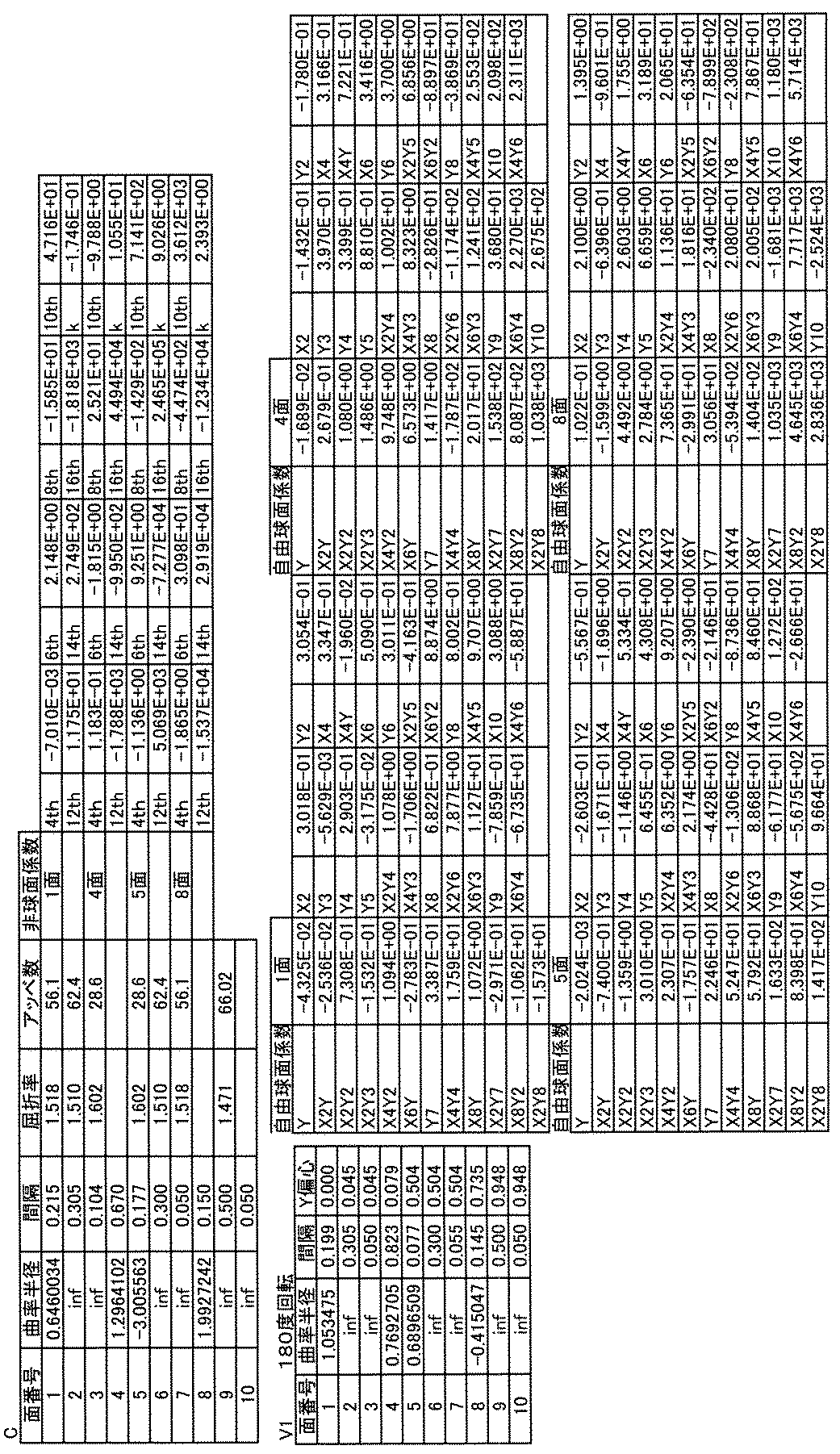
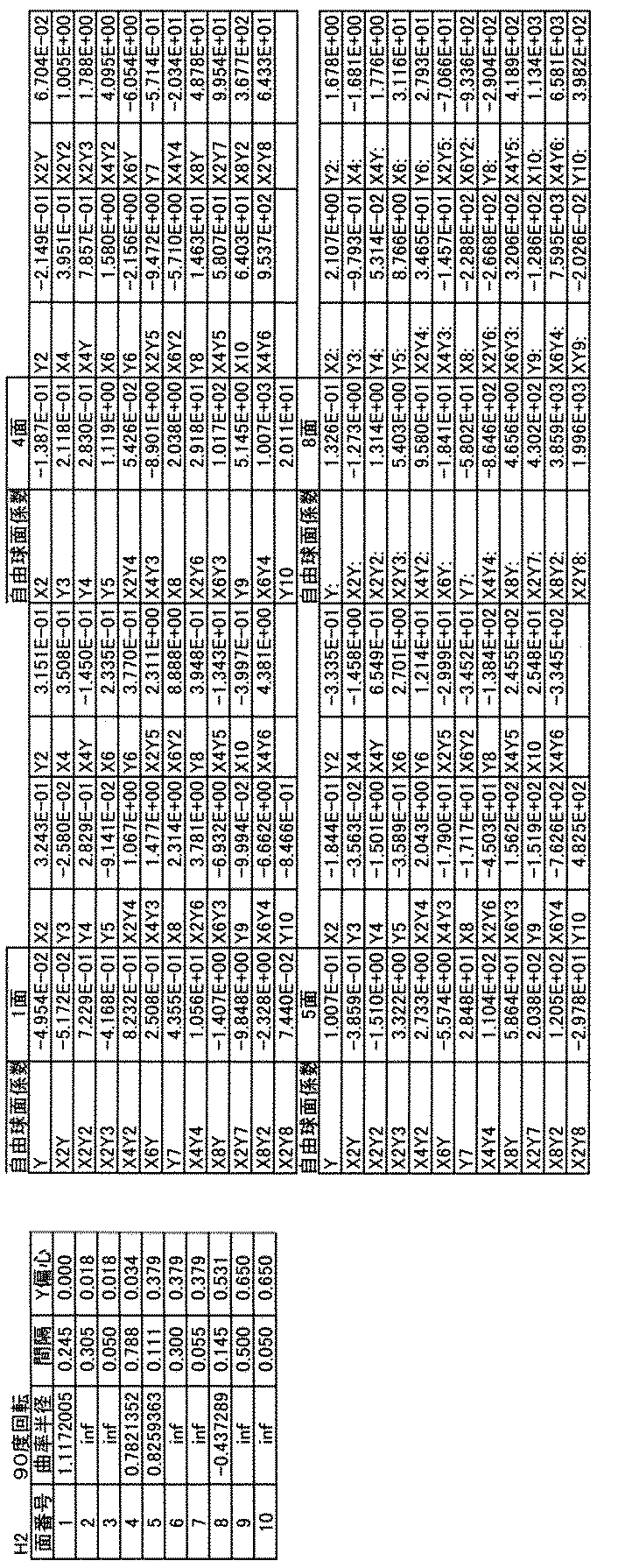
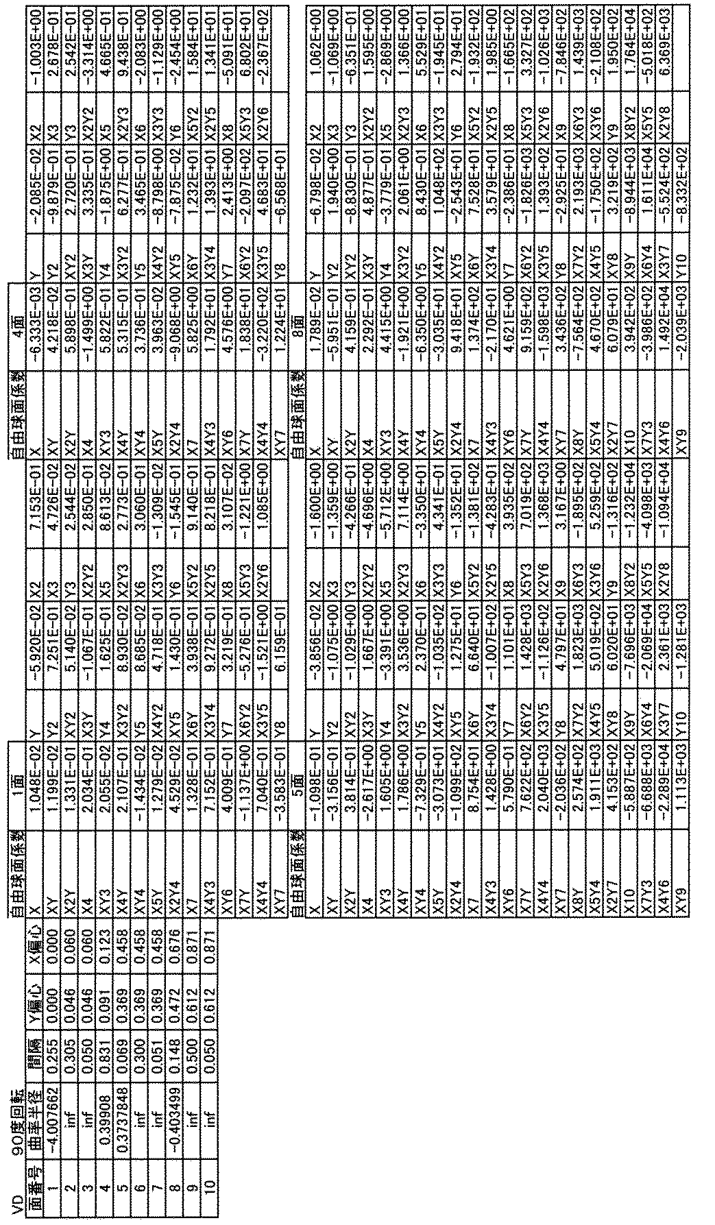
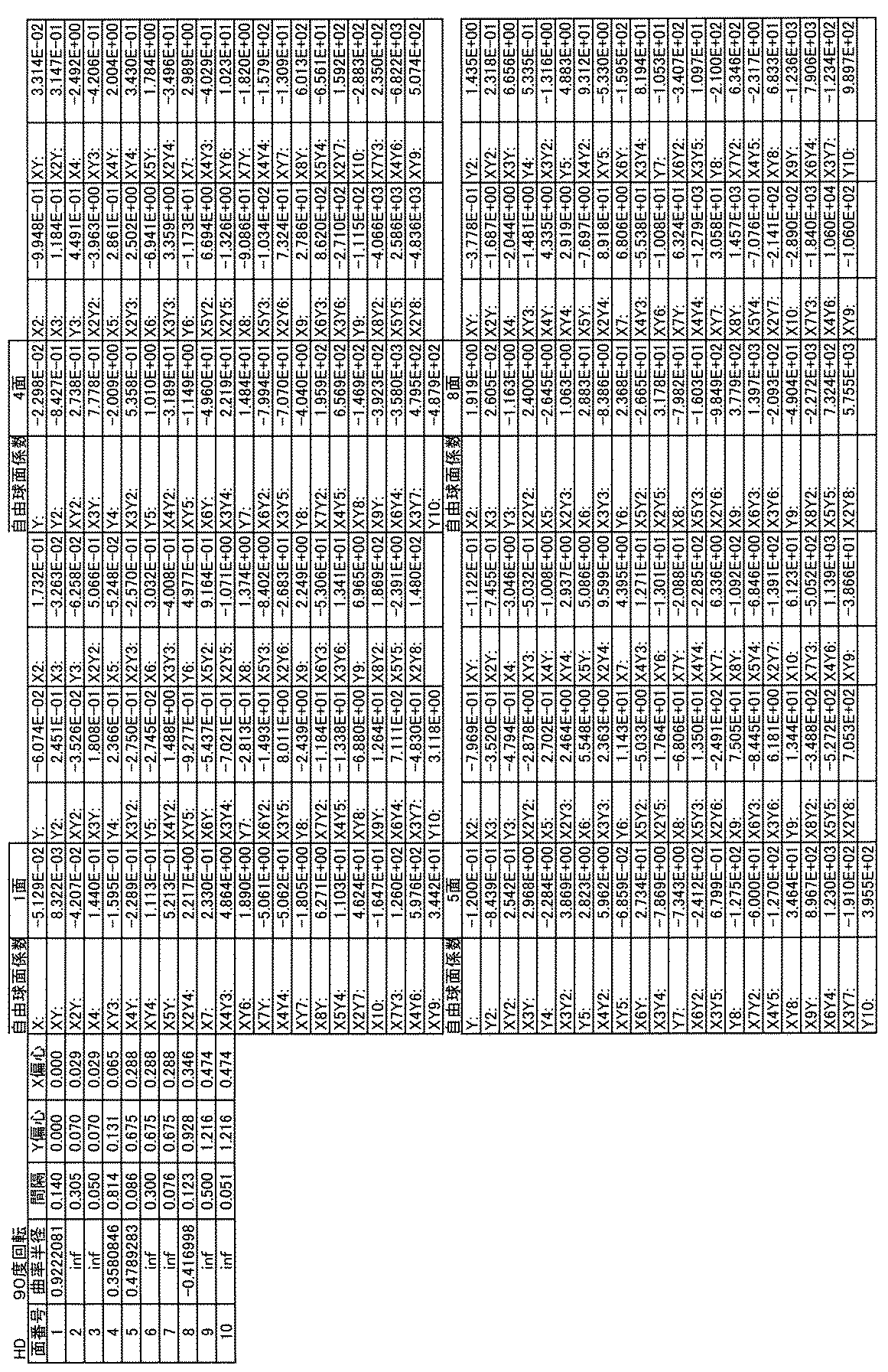
- Table 1 shows the area arrangement of the single lens Ln in the example and the comparative example.
- the single lens Ln is arranged at 5 ⁇ 5 positions, and the entire optical system L0 is arranged at 3 positions. However, since the single lens Ln is symmetrically arranged vertically and horizontally, only 9 positions (C, V1, V2, H1, H2, D1, D2, VD, HD) are shown (common to the comparative example).
- r (mm), shaft upper surface distance d (mm), and Y eccentricity (mm) are shown.
- the “90 degree rotation” of the single lens Ln means that a state in which a surface is created according to the construction data and rotated 90 degrees around the Z axis is the lens state. Therefore, the eccentric direction and the free-form surface coefficient are the same as when X and Y are interchanged (the H direction corresponds to the X direction and the V direction corresponds to the Y direction).
- the central single lens Ln (position: C) that is rotationally symmetric about the optical axis AX uses an aspherical surface that is rotationally symmetric about the optical axis AX. It is defined by the following equation (AS) using an orthogonal coordinate system (X, Y, Z). A free-form surface is used for the peripheral single-lens Ln (position: V1, VD, D1, V2, D2, HD, H2, H1), which is a decentered optical system, and the free-form surface has its surface vertex. It is defined by the following equation (FS) using a local orthogonal coordinate system (X, Y, Z) as the origin.
- AS orthogonal coordinate system
- FS a local orthogonal coordinate system
- the aspheric coefficient is shown as aspheric data, and the free-form surface coefficient is shown as free-form surface data (where A (j, k) is expressed as X j ⁇ Y k ).
- FIG. 7A is a schematic diagram showing the imaging range of the comparative example
- FIG. 7B is a schematic diagram showing the imaging range of the example
- FIG. 7C is an arrangement of the compound eye optical system.
- FIG. Table 4 is a table showing the photographing range and optical system data of each individual lens in the example
- Table 5 is a table showing the photographing range and optical system data of each individual lens in the comparative example.
- the following shooting range VD, D2, H2, D1, HD, and H1 satisfy the following expression (1), and the surrounding shooting range D1 satisfies the following expression (2).
- FIGS. 8A, 8B, 8C, and 8D are graphs showing the MTF values in the imaging ranges D1, V1, H1, and C of the comparative example.
- FIGS. (D) is a graph showing MTF values in the imaging ranges D1, V1, H1, and C of the example. 8A to 8D and FIGS. 9A to 9D are apparently compared with each other, the MTF peak value and the image plane property in the peripheral imaging range are particularly larger than those in the comparative example. The example improved and the effect of the present invention was confirmed.
- the imaging range of the imaging area is reduced by narrowing the imaging range of the peripheral single lens with respect to the imaging range of the central single lens. Since the amount can be reduced, the amount of eccentricity of the lens surface (or the lens group) can be reduced. As a result, it is possible to obtain a single-lens lens having a good imaging performance with little focus shift, and a compound eye optical system having a good imaging performance can be configured.
- the value of the expression (3) or (4) is equal to or greater than the lower limit value, the photographing range of the central single-lens lens is not excessively wide. It is possible to provide a compound eye optical system with good optical performance that is not large.
- three or more individual lenses are arranged in the horizontal direction and the vertical direction. With this configuration, since the photographing range of each single-lens lens can be reduced, the amount of field curvature at the boundary of the photographing range can be reduced, and a compound-eye optical system having good imaging performance can be obtained. .
- the single lens includes at least two lenses, and the peripheral single lens has a free curved surface on at least one surface. Thereby, it can be set as the compound eye optical system which is favorable image formation performance.
- magnification of the single lens is substantially the same. This eliminates the need to align the magnifications of the images when processing the images formed through the individual lenses, thereby simplifying the stitching process of the images and providing a low-cost imaging device. .
- a light-shielding stop between the single-lens lens and the image plane.
- the light-shielding stop it is possible to adopt a configuration that prevents light from entering other than the imaging surface corresponding to each individual eye (to prevent crosstalk), so that a compound eye optical system with good imaging performance is obtained. I can do it.
Landscapes
- Physics & Mathematics (AREA)
- General Physics & Mathematics (AREA)
- Optics & Photonics (AREA)
- Engineering & Computer Science (AREA)
- Multimedia (AREA)
- Signal Processing (AREA)
- Theoretical Computer Science (AREA)
- Lenses (AREA)
- Studio Devices (AREA)
Abstract
Description
少なくとも1枚の一体に形成され、光軸を異ならせた複数のレンズを含むアレイレンズを有し、
各視野に対応して結像を行う複数の個眼レンズが、前記アレイレンズのレンズより構成されており、
(1)式又は(2)式のいずれか少なくとも一方が成立することを特徴とする。
ηh_c > ηh_d (1)
ηv_c > ηv_d (2)
但し、
ηh_c:前記アレイレンズの中心側の中心個眼レンズの水平方向撮影範囲
ηh_d:前記アレイレンズの前記中心個眼レンズよりも周辺側に配置される周辺個眼レンズの水平方向撮影範囲
ηv_c:前記アレイレンズの中心側の中心個眼レンズの垂直方向撮影範囲
ηv_d:前記アレイレンズの前記中心個眼レンズよりも周辺側に配置される周辺個眼レンズの垂直方向撮影範囲
ηh_c > ηh_d (1)
ηv_c > ηv_d (2)
以下、上述した複眼光学系に好適な実施例を、コンストラクションデータ等を挙げて比較例と比較しつつ更に具体的に説明する。ここで挙げる実施例は、上述した実施の形態に対応する数値実施例であり、複眼光学系LHの実施形態を表す光学構成図(図5)は、対応する数値実施例のレンズ構成,光路等を示している。

Z=(C0・h2)/[1+√{1-(1+K)・C02・h2}]+Σ{A(j,k)・Xj・Yk} …(FS)
ただし、
h:Z軸(光軸AX)に対して垂直な方向の高さ(h2=X2+Y2)、
Z:高さhの位置でのZ軸方向の変位量(面頂点基準)、
C0:面頂点での曲率(曲率半径rの逆数)、
K:円錐定数、
Ai:i次の非球面係数、
A(j,k):Xのj次、Yのk次の自由曲面係数、
である。
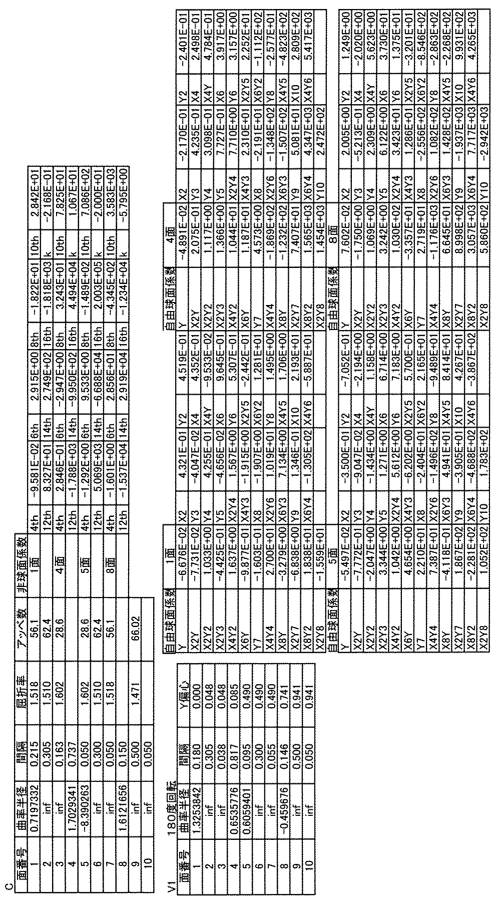
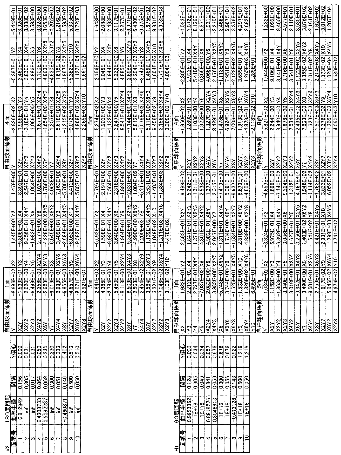

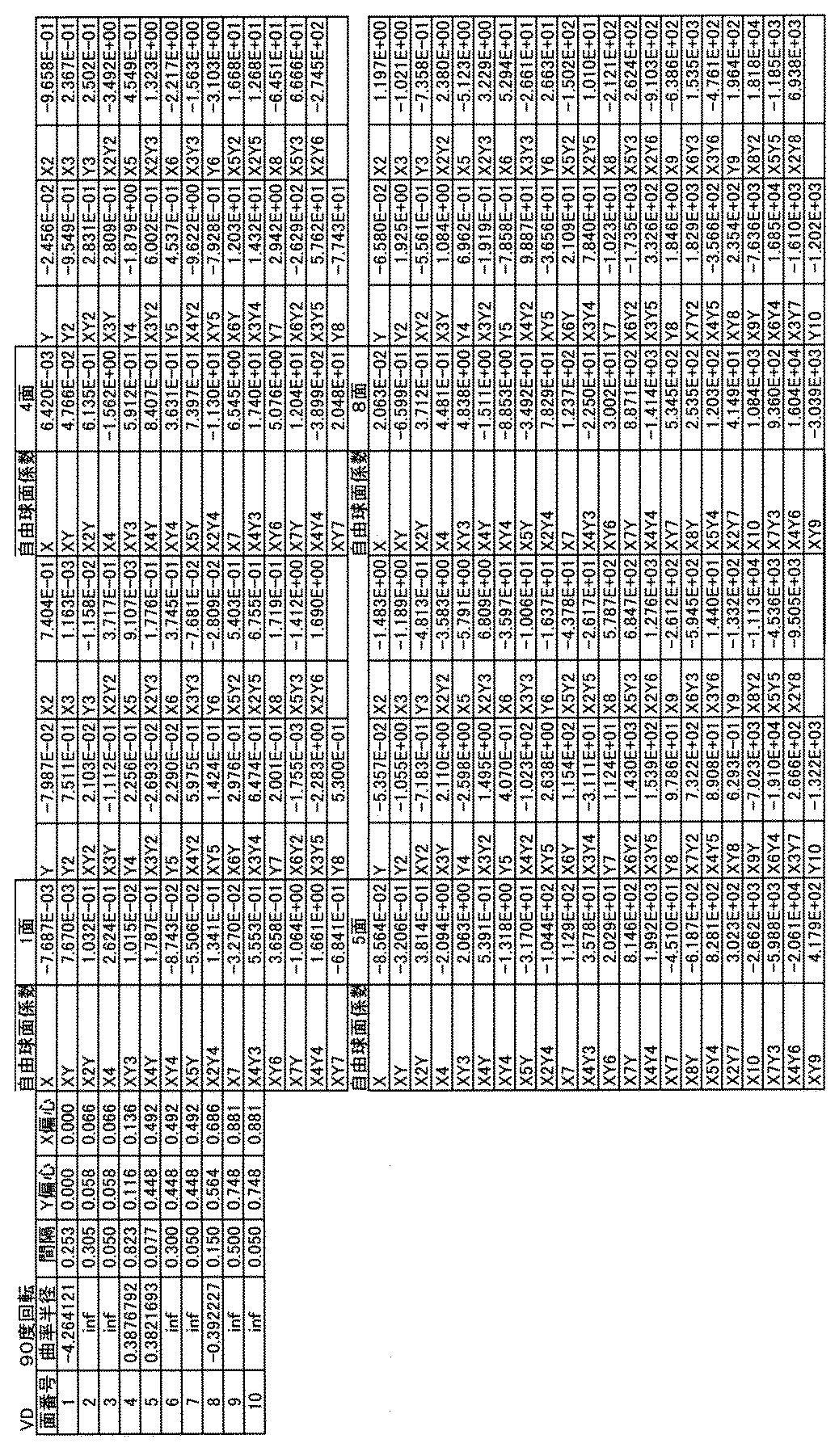


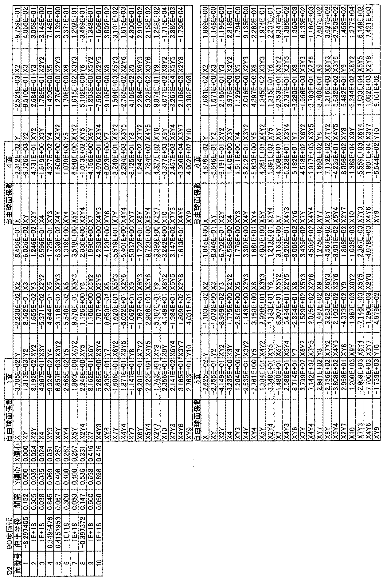
以下は、比較例のコンストラクションデータである。比較例では、各個眼レンズの撮影範囲が等しくなっている。それ以外は、実施例の構成と同様である。




V1: ηh_c = ηh_d、 ηv_c = ηv_d、ηh_d / ηh_c=1,ηv_d / ηv_c=1
V2: ηh_c = ηh_d、 ηv_c = ηv_d、ηh_d / ηh_c=1,ηv_d / ηv_c=1
VD: ηh_c > ηh_d、 ηv_c = ηv_d、ηh_d / ηh_c=0.68,ηv_d / ηv_c=1D2: ηh_c > ηh_d、 ηv_c = ηv_d、ηh_d / ηh_c=0.68,ηv_d / ηv_c=1
H2: ηh_c > ηh_d、 ηv_c = ηv_d、ηh_d / ηh_c=0.68,ηv_d / ηv_c=1
D1: ηh_c > ηh_d、 ηv_c > ηv_d、ηh_d / ηh_c=0.61,ηv_d / ηv_c=7
HD: ηh_c > ηh_d、 ηv_c < ηv_d、ηh_d / ηh_c=0.61,ηv_d / ηv_c=1.2
H1: ηh_c > ηh_d、 ηv_c < ηv_d、ηh_d / ηh_c=0.61,ηv_d / ηv_c=1.2
ηh_c > ηh_d (1)
ηv_c > ηv_d (2)
0.9 ≧ ηh_d / ηh_c ≧ 0.4 (3)
0.9 ≧ ηv_d / ηv_c ≧ 0.4 (4)
1a 画像合成部
1b 画像補正部
1c 出力画像処理部
2 レンズ
3 メモリー
AP 遮光部材
AX 光軸
CG カバーガラス
DL1 中心個眼レンズ
DL2 周辺個眼レンズ
LA1 レンズアレイ
LA2 レンズアレイ
LH 複眼光学系
Ln 個眼レンズ
LU 撮像ユニット
SR 撮像素子
SS 撮像面
Claims (7)
- 1つの固体撮像素子上に形成された、異なる視野の像をつなぎ合わせて1枚の画像を出力する画像処理部を有する撮像装置に用いられる複眼光学系であって、
少なくとも1枚の一体に形成され、光軸を異ならせた複数のレンズを含むアレイレンズを有し、
各視野に対応して結像を行う複数の個眼レンズが、前記アレイレンズのレンズより構成されており、
(1)式又は(2)式のいずれか少なくとも一方が成立することを特徴とする複眼光学系。
ηh_c > ηh_d (1)
ηv_c > ηv_d (2)
但し、
ηh_c:前記アレイレンズの中心側の中心個眼レンズの水平方向撮影範囲
ηh_d:前記アレイレンズの前記中心個眼レンズよりも周辺側に配置される周辺個眼レンズの水平方向撮影範囲
ηv_c:前記アレイレンズの中心側の中心個眼レンズの垂直方向撮影範囲
ηv_d:前記アレイレンズの前記中心個眼レンズよりも周辺側に配置される周辺個眼レンズの垂直方向撮影範囲 - (3)式又は(4)式のいずれか少なくとも一方が成立することを特徴とする複眼光学系。
0.9 ≧ ηh_d / ηh_c ≧ 0.4 (3)
0.9 ≧ ηv_d / ηv_c ≧ 0.4 (4) - 前記個眼レンズは、水平方向、垂直方向にそれぞれ3つ以上並べて配置されていることを特徴とする請求項1又は2に記載の複眼光学系。
- 前記個眼レンズは少なくとも2枚のレンズからなり、前記周辺個眼レンズは少なくとも1面に自由曲面を有することを特徴とする請求項1~3のいずれかに記載の複眼光学系。
- 前記個眼レンズの倍率がほぼ同じであることを特徴とする請求項1~4のいずれかに記載の複眼光学系。
- 前記個眼レンズと像面との間に遮光絞りを有することを特徴とする請求項1~5のいずれかに記載の複眼光学系。
- 請求項1~6のいずれかに記載の複眼光学系と、固体撮像素子と、画像処理部とを有することを特徴とする撮像装置。
Priority Applications (2)
| Application Number | Priority Date | Filing Date | Title |
|---|---|---|---|
| US14/779,503 US20160041311A1 (en) | 2013-03-26 | 2014-03-14 | Compound Eye Optical System And Imaging Device |
| JP2015508297A JPWO2014156712A1 (ja) | 2013-03-26 | 2014-03-14 | 複眼光学系及び撮像装置 |
Applications Claiming Priority (2)
| Application Number | Priority Date | Filing Date | Title |
|---|---|---|---|
| JP2013063922 | 2013-03-26 | ||
| JP2013-063922 | 2013-03-26 |
Publications (1)
| Publication Number | Publication Date |
|---|---|
| WO2014156712A1 true WO2014156712A1 (ja) | 2014-10-02 |
Family
ID=51623694
Family Applications (1)
| Application Number | Title | Priority Date | Filing Date |
|---|---|---|---|
| PCT/JP2014/056851 Ceased WO2014156712A1 (ja) | 2013-03-26 | 2014-03-14 | 複眼光学系及び撮像装置 |
Country Status (3)
| Country | Link |
|---|---|
| US (1) | US20160041311A1 (ja) |
| JP (1) | JPWO2014156712A1 (ja) |
| WO (1) | WO2014156712A1 (ja) |
Cited By (1)
| Publication number | Priority date | Publication date | Assignee | Title |
|---|---|---|---|---|
| CN111190285A (zh) * | 2020-02-18 | 2020-05-22 | 中国人民解放军陆军工程大学 | 多孔径单探测器光学成像系统 |
Families Citing this family (2)
| Publication number | Priority date | Publication date | Assignee | Title |
|---|---|---|---|---|
| JP6297234B1 (ja) * | 2017-06-26 | 2018-03-20 | 三菱電機株式会社 | 複眼撮像装置及び画像処理方法、並びにプログラム及び記録媒体 |
| CN112866512B (zh) * | 2019-11-26 | 2022-03-22 | 中国科学院上海微系统与信息技术研究所 | 复眼摄像装置及复眼系统 |
Citations (4)
| Publication number | Priority date | Publication date | Assignee | Title |
|---|---|---|---|---|
| JP2003161879A (ja) * | 2001-09-13 | 2003-06-06 | Ricoh Co Ltd | 結像光学系、およびそれを用いた画像撮影装置 |
| WO2006101064A1 (ja) * | 2005-03-24 | 2006-09-28 | Matsushita Electric Industrial Co., Ltd. | 撮像装置及びそれに用いられるレンズアレイ |
| WO2007132787A1 (ja) * | 2006-05-15 | 2007-11-22 | Panasonic Corporation | 回折撮像レンズと回折撮像レンズ光学系及びこれを用いた撮像装置 |
| JP2013045032A (ja) * | 2011-08-26 | 2013-03-04 | Fujifilm Corp | 多眼撮像装置 |
Family Cites Families (3)
| Publication number | Priority date | Publication date | Assignee | Title |
|---|---|---|---|---|
| US8204282B2 (en) * | 2007-09-14 | 2012-06-19 | Ricoh Company, Ltd. | Image input device and personal authentication device |
| JP5293950B2 (ja) * | 2008-03-04 | 2013-09-18 | 株式会社リコー | 個人認証装置及び電子機器 |
| JP2012185149A (ja) * | 2011-02-17 | 2012-09-27 | Ricoh Co Ltd | 欠陥検査装置及び欠陥検査処理方法 |
-
2014
- 2014-03-14 JP JP2015508297A patent/JPWO2014156712A1/ja active Pending
- 2014-03-14 US US14/779,503 patent/US20160041311A1/en not_active Abandoned
- 2014-03-14 WO PCT/JP2014/056851 patent/WO2014156712A1/ja not_active Ceased
Patent Citations (4)
| Publication number | Priority date | Publication date | Assignee | Title |
|---|---|---|---|---|
| JP2003161879A (ja) * | 2001-09-13 | 2003-06-06 | Ricoh Co Ltd | 結像光学系、およびそれを用いた画像撮影装置 |
| WO2006101064A1 (ja) * | 2005-03-24 | 2006-09-28 | Matsushita Electric Industrial Co., Ltd. | 撮像装置及びそれに用いられるレンズアレイ |
| WO2007132787A1 (ja) * | 2006-05-15 | 2007-11-22 | Panasonic Corporation | 回折撮像レンズと回折撮像レンズ光学系及びこれを用いた撮像装置 |
| JP2013045032A (ja) * | 2011-08-26 | 2013-03-04 | Fujifilm Corp | 多眼撮像装置 |
Cited By (1)
| Publication number | Priority date | Publication date | Assignee | Title |
|---|---|---|---|---|
| CN111190285A (zh) * | 2020-02-18 | 2020-05-22 | 中国人民解放军陆军工程大学 | 多孔径单探测器光学成像系统 |
Also Published As
| Publication number | Publication date |
|---|---|
| JPWO2014156712A1 (ja) | 2017-02-16 |
| US20160041311A1 (en) | 2016-02-11 |
Similar Documents
| Publication | Publication Date | Title |
|---|---|---|
| JP5041924B2 (ja) | ズームレンズ | |
| KR102052124B1 (ko) | 어안 렌즈계 및 이를 구비한 촬영 장치 | |
| CN108885328B (zh) | 观察光学系统、观察摄像装置、观察摄像系统、成像透镜系统及观察光学系统的调整方法 | |
| KR101412627B1 (ko) | 왜곡이 보정된 광각 촬영 렌즈 시스템 | |
| JP7475483B2 (ja) | カメラモジュールおよび電子デバイス | |
| US20160377838A1 (en) | Optical image capturing system | |
| CN103091819B (zh) | 变焦镜头和包括该变焦镜头的拍摄设备 | |
| TW201715268A (zh) | 影像擷取透鏡系統、取像裝置及電子裝置 | |
| KR20120025338A (ko) | 광각 렌즈계 및 이를 구비한 촬상 장치 | |
| JP2008292800A (ja) | アナモルフィックレンズ、撮像装置及び監視装置 | |
| WO2021065092A1 (ja) | レンズ系、撮像装置及び撮像システム | |
| WO2021065091A1 (ja) | レンズ系、撮像装置及び撮像システム | |
| US20210003819A1 (en) | Rear converter lens and imaging apparatus | |
| WO2022011498A1 (zh) | 光学系统、取像模组及电子装置 | |
| CN111722384B (zh) | 一种变焦镜头 | |
| JP3710352B2 (ja) | ズームレンズ及びそれを用いた光学機器 | |
| KR102335740B1 (ko) | 줌 렌즈 및 이를 포함한 촬영 장치 | |
| CN112526708B (zh) | 摄像光学镜头、摄像头模组和电子设备 | |
| WO2014156712A1 (ja) | 複眼光学系及び撮像装置 | |
| JP2012128033A (ja) | ズームレンズ、カメラおよび携帯情報端末装置 | |
| CN113589501B (zh) | 长焦镜头 | |
| CN112198642B (zh) | 成像透镜 | |
| JP5397063B2 (ja) | 撮像光学系およびカメラ装置および携帯情報端末装置 | |
| TWI617832B (zh) | 影像擷取透鏡系統、取像裝置及電子裝置 | |
| CN115016108B (zh) | 一种变焦镜头及成像装置 |
Legal Events
| Date | Code | Title | Description |
|---|---|---|---|
| 121 | Ep: the epo has been informed by wipo that ep was designated in this application |
Ref document number: 14776321 Country of ref document: EP Kind code of ref document: A1 |
|
| ENP | Entry into the national phase |
Ref document number: 2015508297 Country of ref document: JP Kind code of ref document: A |
|
| WWE | Wipo information: entry into national phase |
Ref document number: 14779503 Country of ref document: US |
|
| NENP | Non-entry into the national phase |
Ref country code: DE |
|
| 122 | Ep: pct application non-entry in european phase |
Ref document number: 14776321 Country of ref document: EP Kind code of ref document: A1 |