WO2014156367A1 - エレクトロルミネッセンス装置、及びその製造方法 - Google Patents
エレクトロルミネッセンス装置、及びその製造方法 Download PDFInfo
- Publication number
- WO2014156367A1 WO2014156367A1 PCT/JP2014/053646 JP2014053646W WO2014156367A1 WO 2014156367 A1 WO2014156367 A1 WO 2014156367A1 JP 2014053646 W JP2014053646 W JP 2014053646W WO 2014156367 A1 WO2014156367 A1 WO 2014156367A1
- Authority
- WO
- WIPO (PCT)
- Prior art keywords
- organic
- substrate
- metal film
- protective film
- electroluminescence
- Prior art date
- Legal status (The legal status is an assumption and is not a legal conclusion. Google has not performed a legal analysis and makes no representation as to the accuracy of the status listed.)
- Ceased
Links
Images

Classifications
-
- H—ELECTRICITY
- H10—SEMICONDUCTOR DEVICES; ELECTRIC SOLID-STATE DEVICES NOT OTHERWISE PROVIDED FOR
- H10K—ORGANIC ELECTRIC SOLID-STATE DEVICES
- H10K59/00—Integrated devices, or assemblies of multiple devices, comprising at least one organic light-emitting element covered by group H10K50/00
- H10K59/80—Constructional details
- H10K59/87—Passivation; Containers; Encapsulations
- H10K59/871—Self-supporting sealing arrangements
- H10K59/8721—Metallic sealing arrangements
-
- H—ELECTRICITY
- H05—ELECTRIC TECHNIQUES NOT OTHERWISE PROVIDED FOR
- H05B—ELECTRIC HEATING; ELECTRIC LIGHT SOURCES NOT OTHERWISE PROVIDED FOR; CIRCUIT ARRANGEMENTS FOR ELECTRIC LIGHT SOURCES, IN GENERAL
- H05B33/00—Electroluminescent light sources
- H05B33/02—Details
- H05B33/04—Sealing arrangements, e.g. against humidity
Definitions
- the present invention relates to an electroluminescence device having an EL (electroluminescence) element, and a manufacturing method thereof.
- flat panel displays have been used in various products and fields, and further flat panel displays are required to have larger sizes, higher image quality, and lower power consumption.
- an organic EL display device equipped with an organic EL (electroluminescence) element using electroluminescence of an organic material is an all-solid-state type, can be driven at a low voltage, has high-speed response, and self-emission.
- an organic EL display device equipped with an organic EL (electroluminescence) element using electroluminescence of an organic material is an all-solid-state type, can be driven at a low voltage, has high-speed response, and self-emission.
- a thin-film organic EL element is provided on a substrate on which a TFT (thin film transistor) is provided.
- TFT thin film transistor
- an organic EL layer including a light emitting layer is laminated between a pair of electrodes.
- a TFT is connected to one of the pair of electrodes.
- An image is displayed by applying a voltage between the pair of electrodes to cause the light emitting layer to emit light.
- the front and side surfaces of the substrate on which the organic EL element is provided can be protected by an organic protective film. Proposed. And in this conventional organic electroluminescence display and its manufacturing method, it was made possible to improve the stability of a subsequent process.
- an object of the present invention is to provide a long-life electroluminescence device capable of preventing the electroluminescence element from being adversely affected by moisture, and a method for manufacturing the same.
- an electroluminescence device is an electroluminescence device including a substrate and an electroluminescence element provided on the substrate, A protective film for covering the electroluminescent element and protecting the electroluminescent element on the substrate; A frame-shaped sealing material that surrounds the protective film on the substrate, and a metal film that is bonded to the substrate by the sealing material and that seals the electroluminescent element and the protective film between the substrate and the substrate It is characterized by having.
- a metal film is bonded to a substrate with a sealing material, and the electroluminescence element and the protective film provided on the substrate are sealed.
- a long-life electroluminescence device that can prevent the adverse effect of moisture on the electroluminescence element.
- the metal film is preferably aluminum.
- an electroluminescence device that is easy to manufacture can be configured.
- the thickness of the metal film is preferably in the range of 1 ⁇ m to 50 ⁇ m.
- the protective film is preferably made of an inorganic material.
- the method for manufacturing an electroluminescence device of the present invention is a method for manufacturing an electroluminescence device including a substrate and an electroluminescence element provided on the substrate, An electroluminescence element forming step of forming an electroluminescence element on the substrate; A protective film forming step of forming a protective film so as to cover the electroluminescence element on the substrate; In a vacuum atmosphere, a metal film installation step of providing a metal film on the side opposite to the substrate of the protective film so as to face the substrate; A pressing step of pressing the metal film against the substrate in a vacuum atmosphere; And a bonding step of bonding the substrate and the metal film with a frame-shaped sealing material surrounding the protective film.
- the metal film is pressed to the substrate side in a vacuum atmosphere during the pressing step.
- the bonding step the substrate and the metal film are bonded by a frame-shaped sealing material that surrounds the protective film.
- the vacuum atmosphere preferably has a degree of vacuum of 100 Pascal or less.
- the metal film can be pressed and bonded to the substrate appropriately and reliably.
- the present invention it is possible to provide a long-life electroluminescence device that can prevent the adverse effect of moisture on the electroluminescence element, and a method for manufacturing the electroluminescence device.
- FIG. 1 is a cross-sectional view illustrating an organic EL display device according to a first embodiment of the present invention.
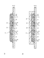
- FIG. 2 is a diagram for explaining main manufacturing steps of the organic EL display device, and FIGS. 2A to 2B show a series of main manufacturing steps.
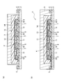
- FIG. 3 is a diagram for explaining the main manufacturing process of the organic EL display device.
- FIGS. 3A to 3B are a series of steps performed subsequent to the manufacturing process shown in FIG. The main manufacturing process is described.
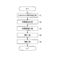
- FIG. 4 is a flowchart for explaining main manufacturing steps of the organic EL display device.
- FIG. 1 is a cross-sectional view illustrating an organic EL display device according to a first embodiment of the present invention.
- an organic EL display device 1 according to the present embodiment includes a TFT substrate 2 as a substrate and an organic EL element 4 as an electroluminescence element provided on the TFT substrate 2.
- the organic EL element 4 is provided between the TFT substrate 2, the metal film 3 provided so as to face the TFT substrate 2, and the TFT substrate 2 and the metal film 3. It is sealed with a sealing material 5 that bonds the metal film 3.
- the organic EL element 4 forms a pixel region A having a plurality of pixels, and the organic EL element 4 is formed in a TFT substrate 2, a metal film 3, and a frame shape. It is arranged inside the space surrounded by the provided sealing material 5.
- the pixel area A constitutes the display unit of the organic EL display device 1 and displays information.
- the TFT substrate 2 is made of, for example, a glass material. Further, the TFT substrate 2 is provided with a base film (insulating film) 6 so as to cover the entire surface, and a TFT (thin film transistor) 7 is provided for each pixel in the pixel region A on the base film 6. ing. On the base film 6, wirings 8 including a plurality of source lines (signal lines) and a plurality of gate lines provided in a matrix are formed. A source driver and a gate driver are respectively connected to the source line and the gate line (not shown), and the TFT 7 for each pixel is driven in accordance with an image signal input from the outside.
- the TFT 7 functions as a switching element that controls the light emission of the corresponding pixel, and any one of red (R), green (G), and blue (B) formed by the organic EL element 4 is used. The light emission at these pixels is controlled.
- the base film 6 is for preventing the characteristics of the TFT 7 from deteriorating due to impurity diffusion from the TFT substrate 2 to the TFT 7. If there is no concern about such deterioration, the base film 6 may be omitted. it can.
- an interlayer insulating film 9, an edge cover 10, and a first electrode 11 of the organic EL element 4 are formed on the TFT substrate 2, on the TFT substrate 2, an interlayer insulating film 9, an edge cover 10, and a first electrode 11 of the organic EL element 4 are formed.
- the interlayer insulating film 9 also functions as a planarizing film, and is provided on the base film 6 so as to cover the TFT 7 and the wiring 8.
- the edge cover 10 is formed on the interlayer insulating film 9 so as to cover the pattern end of the first electrode 11.
- the edge cover 10 also functions as an insulating layer for preventing a short circuit between the first electrode 11 and a second electrode 13 described later.
- the first electrode 11 is connected to the TFT 7 through a contact hole formed in the interlayer insulating film 9.
- the opening of the edge cover 10, that is, the portion where the first electrode 11 is exposed substantially constitutes the light emitting region of the organic EL element 4, and emits one of RGB color lights as described above.
- the organic EL display device 1 of the present embodiment is configured so that full color display can be performed.
- the organic EL layer 12 and the second electrode 13 are formed on the first electrode 11, and the organic EL element 4 is configured by the first electrode 11, the organic EL layer 12, and the second electrode 13.
- the organic EL element 4 is a light emitting element that can emit light with high luminance by, for example, low-voltage direct current driving, and includes a first electrode 11, an organic EL layer 12, and a second electrode 13.
- the organic EL layer 12 when the first electrode 11 is an anode, the organic EL layer 12 includes a hole injection layer, a hole transport layer, a light emitting layer, an electron transport layer, an electron injection layer, and the like from the first electrode 11 side. Laminated (not shown), and further, a second electrode 13 as a cathode is formed. In addition to this description, a single layer may have two or more functions such as a hole injection layer / hole transport layer. In the organic EL layer 12, a carrier blocking layer or the like may be appropriately inserted.
- the layer order in the organic EL layer 12 is reversed from the above.
- the organic EL display device 1 is a bottom emission type in which light is emitted from the TFT substrate 2 side.
- the organic EL display device 1 is a top emission type that emits light from the counter substrate 3 side.
- the protective film 14 that covers the organic EL element 4 and protects the organic EL element 4 is provided on the TFT substrate 2.
- the protective film 14 is made of, for example, an inorganic material such as SiNx, SiN, SiON, or Al 2 O 3 , and protects the organic EL element 4 from being damaged by the ingress of moisture or oxygen from the outside. It is supposed to do.
- metal film 3 is used for the metal film 3.
- metal film 3 for example, an aluminum thin film having a value in the range of 1 ⁇ m to 50 ⁇ m is used.
- the metal film 3 is bonded to the TFT substrate 2 in a vacuum atmosphere, and the TFT is sealed on the TFT substrate 2 by the frame-shaped sealing material 5 surrounding the protective film 14. It is adapted to be bonded to the substrate 2.
- an ultraviolet curable resin such as an epoxy resin and / or a thermosetting resin is used.
- FIG. 2 is a diagram for explaining main manufacturing steps of the organic EL display device, and FIGS. 2A to 2B show a series of main manufacturing steps.
- FIG. 3 is a diagram for explaining the main manufacturing process of the organic EL display device.
- FIGS. 3A to 3B are a series of steps performed subsequent to the manufacturing process shown in FIG. The main manufacturing process is described.
- FIG. 4 is a flowchart for explaining main manufacturing steps of the organic EL display device.
- an electroluminescence element forming step for forming an organic EL element (electroluminescence element) 4 on the TFT substrate (substrate) 2 is performed. . That is, as shown in FIG. 2A, after the base film 6 is formed so as to cover the entire surface of the TFT substrate 2, each part of the organic EL element 4 is sequentially formed by a known manufacturing method, and the organic EL An element 4 is formed on the TFT substrate 2.
- a protective film forming process for forming the protective film 14 is performed so as to cover the organic EL element 4 on the TFT substrate 2. That is, as shown in FIG. 2B, the protective film 14 is formed on the TFT substrate 2 so as to cover the organic EL element 4 by, for example, sputtering or CVD.
- a metal film installation step of providing a metal film 3 on the opposite side of the protective film 14 from the TFT substrate 2 so as to face the TFT substrate 2 is performed.
- a vacuum is formed inside a vacuum bonding apparatus (not shown).
- the metal film 3 is provided on the protective film 14.
- a pressing step of pressing the metal film 3 toward the TFT substrate 2 is performed in a vacuum atmosphere. Specifically, the metal film 3 is pressed toward the TFT substrate 2 in the vacuum bonding apparatus. As a result, as shown in FIG. 3B, the metal film 3 is pressed and deformed, and the metal film 3 is bonded to the TFT substrate 2, the sealing material 5, and the protective film 14. .
- an adhesion process for bonding the TFT substrate 2 and the metal film 3 is performed by the frame-shaped sealing material 5 surrounding the protective film 14. That is, in FIG. 3B, the sealing material 5 is irradiated with, for example, ultraviolet rays (for example, 0.5 J to 10 J, desirably 1 J to 6 J), and then heated (for example, 70 ° C. to 120 ° C. The TFT substrate 2 and the metal film 3 are bonded to each other by the sealing material 5. Thereby, the organic EL display device 1 of the present embodiment is completed.
- ultraviolet rays for example, 0.5 J to 10 J, desirably 1 J to 6 J
- this bonding step may be performed inside the above-described vacuum bonding apparatus, or may be performed outside the vacuum bonding apparatus.
- the vacuum atmosphere is, for example, a vacuum degree of 100 Pascal (Pa) or less.
- the metal film 3 can be pressed and bonded to the TFT substrate 2 appropriately and surely.
- the metal film 3 since the metal film 3 is bonded so as to be in close contact with the protective film 14 made of an inorganic material, even if the protective film 14 has irregularities such as pinholes and cracks, the metal film 3 covers the metal film 3.
- the barrier property and moisture resistance of the organic EL display device 1 of the present embodiment can be greatly improved.
- the metal film 3 can prevent the organic EL element 4 from being damaged due to the cracks or the like in the protective film 14.
- the frame-shaped sealing material 5 may be provided on the metal film 3 side.
- the metal film 3 is bonded to the TFT substrate (substrate) 2 by the sealing material 5 and the organic EL element (on the TFT substrate 2) ( The electroluminescent element) 4 and the protective film 14 are sealed.
- the organic EL display device (electroluminescence device) 1 having a long lifetime that can prevent the organic EL element 4 from being adversely affected by moisture can be easily configured. it can.
- the thickness of the metal film 3 is a value within the range of 1 ⁇ m to 50 ⁇ m.
- the metal film 3 can be formed by using another forming method (film forming method) such as a vapor deposition method, a CVD method, or a sputtering method.
- film forming method such as a vapor deposition method, a CVD method, or a sputtering method.
- a dedicated manufacturing apparatus is required, and it takes a lot of time and cost to form the film. This causes the problem.
- the metal film 3 having the thickness as described above is formed by using these forming methods, another problem that the film becomes easier to peel off as the film thickness is increased, or the organic EL element 4 is affected. As the film forming process becomes longer, another problem that an adverse effect (damage) is likely to occur may occur.
- the metal film 3 is bonded to the TFT substrate 2 in a vacuum atmosphere, so that the organic EL display device 1 can be easily configured at a low cost with simple manufacturing. can do. Further, it is possible to prevent the organic EL element 4 from being damaged.
- an organic EL element is used as an electroluminescence element.
- the present invention is not limited to this, and for example, an inorganic EL element having an inorganic compound may be used.
- the present invention is not limited to this, and can be applied to an illumination device such as a backlight device.
- the metal film of the present invention is not limited to this, for example, a metal such as stainless steel or nickel, or these metals or aluminum.
- a structure using a metal thin film such as an alloy of the above may be used.
- the protective film is made of an inorganic material.
- the protective film of the present invention is not limited to this, and for example, an organic EL element (electroluminescence element)
- the structure which forms the protective film which consists of an organic material and an inorganic material sequentially may be sufficient.
- the protective film made of an inorganic material when used, the adverse effect of moisture occurs on the electroluminescent element as compared with the case of forming a protective film containing an organic material. Is preferable in that it can be surely prevented. That is, it is preferable in that it is possible to reliably prevent moisture and organic components contained in the organic material itself from reaching the electroluminescence element and adversely affecting it.
- the present invention is useful for a long-life electroluminescence device capable of preventing the adverse effect of moisture on the electroluminescence element, and a method for manufacturing the same.
- Organic EL display device TFT substrate (substrate) 3 Metal film 4 Organic EL device (electroluminescence device) 5 Sealing material 14 Protective film
Landscapes
- Electroluminescent Light Sources (AREA)
Abstract
有機EL素子(エレクトロルミネッセンス素子)(4)を具備した有機EL表示装置(エレクトロルミネッセンス装置)(1)において、TFT基板(基板)(2)で、有機EL素子(4)を覆って当該有機EL素子(4)を保護する保護膜(14)、TFT基板(2)上で、保護膜(14)を囲んだ枠状のシール材(5)、及びシール材(5)によってTFT基板(2)に接着されるとともに、当該TFT基板(2)との間で有機EL素子(4)及び保護膜(14)を封止する金属膜(3)を備える。
Description
本発明は、EL(エレクトロルミネッセンス)素子を有するエレクトロルミネッセンス装置、及びその製造方法に関する。
近年、様々な商品や分野でフラットパネルディスプレイが活用されており、フラットパネルディスプレイのさらなる大型化、高画質化、低消費電力化が求められている。
そのような状況下、有機材料の電界発光(Electro Luminescence)を利用した有機EL(エレクトロルミネッセンス)素子を備えた有機EL表示装置は、全固体型で、低電圧駆動可能、高速応答性、自発光性等の点で優れたフラットパネルディスプレイとして、高い注目を浴びている。
例えばアクティブマトリクス方式の有機EL表示装置では、TFT(薄膜トランジスタ)が設けられた基板上に薄膜状の有機EL素子が設けられている。有機EL素子では、一対の電極の間に発光層を含む有機EL層が積層されている。一対の電極の一方にTFTが接続されている。そして、一対の電極間に電圧を印加して発光層を発光させることにより画像表示が行われる。
また、従来の有機EL表示装置及びその製造方法には、例えば下記特許文献1に記載されているように、有機保護膜によって、有機EL素子を設けた基板の前面と側面すべてを保護することが提案されている。そして、この従来の有機EL表示装置及びその製造方法では、後の工程の安定性を向上させることが可能とされていた。
しかしながら、上記のような従来の有機EL表示装置(エレクトロルミネッセンス装置)及びその製造方法では、有機EL素子(エレクトロルミネッセンス素子)に水分の悪影響が生じるのを防ぐことができず、有機EL表示装置の長寿命化を図ることが難しいという問題点があった。
具体的にいえば、この従来の有機EL表示装置及びその製造方法では、有機保護膜により、有機EL素子を覆っていたので、外部からの水分が有機保護膜を透過して有機EL素子に達したり、有機保護膜自体に含まれた水分が有機EL素子に達したりすることがあった。このため、この従来の有機EL表示装置及びその製造方法では、有機EL素子が水分によって劣化して、画素が損傷したり、表示品位が低下したりするという問題点を生じた。また、この結果、この従来の有機EL表示装置及びその製造方法では、有機EL表示装置の長寿命化を図ることが困難なものとなった。
上記の課題を鑑み、本発明は、エレクトロルミネッセンス素子に水分の悪影響が生じるのを防ぐことができる長寿命なエレクトロルミネッセンス装置、及びその製造方法を提供することを目的とする。
上記の目的を達成するために、本発明にかかるエレクトロルミネッセンス装置は、基板と、前記基板上に設けられたエレクトロルミネッセンス素子を備えたエレクトロルミネッセンス装置であって、
前記基板上で、前記エレクトロルミネッセンス素子を覆って当該エレクトロルミネッセンス素子を保護する保護膜、
前記基板上で、前記保護膜を囲んだ枠状のシール材、及び
前記シール材によって前記基板に接着されるとともに、当該基板との間で前記エレクトロルミネッセンス素子及び前記保護膜を封止する金属膜を備えていることを特徴とするものである。
前記基板上で、前記エレクトロルミネッセンス素子を覆って当該エレクトロルミネッセンス素子を保護する保護膜、
前記基板上で、前記保護膜を囲んだ枠状のシール材、及び
前記シール材によって前記基板に接着されるとともに、当該基板との間で前記エレクトロルミネッセンス素子及び前記保護膜を封止する金属膜を備えていることを特徴とするものである。
上記のように構成されたエレクトロルミネッセンス装置では、金属膜がシール材によって基板に接着されて、当該基板上に設けられたエレクトロルミネッセンス素子及び保護膜を封止している。これにより、上記従来例と異なり、エレクトロルミネッセンス素子に水分の悪影響が生じるのを防ぐことができる長寿命なエレクトロルミネッセンス装置を容易に構成することができる。
また、上記エレクトロルミネッセンス装置において、前記金属膜は、アルミニウムであることが好ましい。
この場合、製造簡単なエレクトロルミネッセンス装置を構成することができる。
また、上記エレクトロルミネッセンス装置において、前記金属膜の厚みが、1μm~50μmの範囲内の値であることが好ましい。
この場合、エレクトロルミネッセンス装置の重量が重くなりすぎるのを防ぎつつ、エレクトロルミネッセンス素子に水分の悪影響が生じるのを防ぐことができる長寿命なエレクトロルミネッセンス装置を容易に構成することができる。
また、上記エレクトロルミネッセンス装置において、前記保護膜が、無機材料によって構成されていることが好ましい。
この場合、有機材料を含んだ保護膜を構成する場合に比べて、エレクトロルミネッセンス素子に水分の悪影響が生じるのを確実に防ぐことができる。
また、本発明のエレクトロルミネッセンス装置の製造方法は、基板と、前記基板上に設けられたエレクトロルミネッセンス素子を備えたエレクトロルミネッセンス装置の製造方法であって、
前記基板上に、エレクトロルミネッセンス素子を形成するエレクトロルミネッセンス素子形成工程と、
前記基板上のエレクトロルミネッセンス素子を覆うように、保護膜を形成する保護膜形成工程と、
真空雰囲気下において、前記保護膜の前記基板とは反対側に、当該基板と対向するように金属膜を設ける金属膜設置工程と、
真空雰囲気下において、前記金属膜を前記基板側に押圧する押圧工程と、
前記保護膜を囲んだ枠状のシール材により、前記基板と前記金属膜とを接着する接着工程とを備えていることを特徴とするものである。
前記基板上に、エレクトロルミネッセンス素子を形成するエレクトロルミネッセンス素子形成工程と、
前記基板上のエレクトロルミネッセンス素子を覆うように、保護膜を形成する保護膜形成工程と、
真空雰囲気下において、前記保護膜の前記基板とは反対側に、当該基板と対向するように金属膜を設ける金属膜設置工程と、
真空雰囲気下において、前記金属膜を前記基板側に押圧する押圧工程と、
前記保護膜を囲んだ枠状のシール材により、前記基板と前記金属膜とを接着する接着工程とを備えていることを特徴とするものである。
上記のように構成されたエレクトロルミネッセンス装置の製造方法では、押圧工程の際に、真空雰囲気下において、金属膜を基板側に押圧している。そして、接着工程において、保護膜を囲んだ枠状のシール材により、前記基板と前記金属膜とを接着している。これにより、上記従来例と異なり、エレクトロルミネッセンス素子に水分の悪影響が生じるのを防ぐことができる長寿命なエレクトロルミネッセンス装置を容易に構成することができる。
また、上記エレクトロルミネッセンス装置の製造方法において、前記真空雰囲気は、100パスカル以下の真空度であることが好ましい。
この場合、金属膜を基板に適切に、かつ、確実に押圧して貼り合わせることができる。
本発明によれば、エレクトロルミネッセンス素子に水分の悪影響が生じるのを防ぐことができる長寿命なエレクトロルミネッセンス装置、及びその製造方法を提供することが可能となる。
以下、本発明のエレクトロルミネッセンス装置、及びその製造方法を示す好ましい実施形態について、図面を参照しながら説明する。なお、以下の説明では、本発明を有機EL表示装置に適用した場合を例示して説明する。また、各図中の構成部材の寸法は、実際の構成部材の寸法及び各構成部材の寸法比率等を忠実に表したものではない。
[第1の実施形態]
図1は、本発明の第1の実施形態にかかる有機EL表示装置を説明する断面図である。図1において、本実施形態の有機EL表示装置1は、基板としてのTFT基板2、及びこのTFT基板2上に設けられたエレクトロルミネッセンス(Electro Luminescence)素子としての有機EL素子4を備えている。また、有機EL素子4は、TFT基板2と、このTFT基板2に対向するように設けられた金属膜3と、TFT基板2と金属膜3との間に設けられて、これらTFT基板2と金属膜3とを接着するシール材5とによって封入されている。
図1は、本発明の第1の実施形態にかかる有機EL表示装置を説明する断面図である。図1において、本実施形態の有機EL表示装置1は、基板としてのTFT基板2、及びこのTFT基板2上に設けられたエレクトロルミネッセンス(Electro Luminescence)素子としての有機EL素子4を備えている。また、有機EL素子4は、TFT基板2と、このTFT基板2に対向するように設けられた金属膜3と、TFT基板2と金属膜3との間に設けられて、これらTFT基板2と金属膜3とを接着するシール材5とによって封入されている。
つまり、本実施形態の有機EL表示装置1では、有機EL素子4が複数の画素を有する画素領域Aを構成しており、この有機EL素子4はTFT基板2及び金属膜3、及び枠状に設けられたシール材5によって囲まれた空間の内部に配置されている。また、上記画素領域Aは、有機EL表示装置1の表示部を構成しており、情報表示を行うようになっている。
また、図1において、TFT基板2は、例えばガラス材により、構成されている。また、TFT基板2には、その全面を覆うように下地膜(絶縁膜)6が設けられており、この下地膜6上には、TFT(薄膜トランジスタ)7が画素領域Aの画素毎に設けられている。また、下地膜6上には、マトリクス状に設けられた複数のソース線(信号線)及び複数のゲート線を含んだ配線8が形成されている。ソース線及びゲート線には、それぞれソースドライバ及びゲートドライバが接続されており(図示せず)、外部から入力された画像信号に応じて、画素毎のTFT7を駆動するようになっている。また、TFT7は、対応する画素の発光を制御するスイッチング素子として機能するものであり、有機EL素子4によって構成された赤色(R)、緑色(G)、及び青色(B)のいずれかの色の画素での発光を制御するようになっている。
なお、下地膜6は、TFT基板2からTFT7への不純物拡散によりTFT7の特性が劣化するのを防止するためのものであり、そのような劣化が懸念されないのであれば、設置を省略することができる。
また、TFT基板2上には、層間絶縁膜9、エッジカバー10、及び有機EL素子4の第一電極11が形成されている。層間絶縁膜9は、平坦化膜としても機能するものであり、TFT7及び配線8を覆うように下地膜6上に設けられている。エッジカバー10は、層間絶縁膜9上に、第一電極11のパターン端部を被覆するように形成されている。また、エッジカバー10は、第一電極11と後述の第二電極13との短絡を防止するための絶縁層としても機能するようになっている。また、第一電極11は、層間絶縁膜9に形成されたコンタクトホールを介してTFT7に接続されている。
また、エッジカバー10の開口部、つまり第一電極11が露出した部分が、有機EL素子4の発光領域を実質的に構成しており、上述したように、RGBのいずれかの色光を発光して、フルカラー表示が行えるように、本実施形態の有機EL表示装置1は構成されている。
また、第一電極11上には、有機EL層12及び第二電極13が形成されており、これらの第一電極11、有機EL層12、及び第二電極13により、有機EL素子4が構成されている。すなわち、有機EL素子4は、例えば低電圧直流駆動による高輝度発光が可能な発光素子であり、第一電極11、有機EL層12、及び第二電極13を備えている。
具体的にいえば、第一電極11が陽極である場合、第一電極11側より、正孔注入層、正孔輸送層、発光層、電子輸送層、電子注入層等が有機EL層12として積層され(図示せず)、さらに陰極としての第二電極13が形成される。また、この説明以外に、正孔注入層兼正孔輸送層などのように、単一の層が2つ以上の機能を有する構成でもよい。また、有機EL層12において、キャリアブロッキング層などを適宜挿入してもよい。
一方、第二電極13が陽極である場合には、有機EL層12での層順が上述のものと逆転したものとなる。
また、第一電極11を透過電極あるいは半透過電極にて構成し、第二電極13を反射電極にて構成した場合、有機EL表示装置1はTFT基板2側から光出射するボトムエミッション型となる。逆に、第一電極11を反射電極にて構成し、第二電極13を透過電極あるいは半透過電極にて構成した場合、有機EL表示装置1は対向基板3側から光出射するトップエミッション型となる。
また、本実施形態の有機EL表示装置1では、TFT基板2上で、有機EL素子4を覆って当該有機EL素子4を保護する保護膜14が設けられている。この保護膜14は、例えばSiNx、SiN、SiON、あるいはAl2O3などの無機材料によって構成されており、外部からの水分や酸素の浸入によって有機EL素子4が損傷を受けないように、保護するようになっている。
また、金属膜3には、例えばアルミニウムが用いられている。また、この金属膜3には、例えば1μm~50μmの範囲内の値のアルミニウム薄膜が使用されている。そして、この金属膜3は、後に詳述するように、真空雰囲気下において、TFT基板2に貼り合わせられるとともに、TFT基板2上で、保護膜14を囲んだ枠状の上記シール材5によってTFT基板2に接着されるようになっている。
また、シール材5には、例えばエポキシ樹脂などの紫外線硬化樹脂及び/または熱硬化樹脂が用いられている。
次に、図2~図4を用いて、本実施形態の有機EL表示装置1の製造方法について具体的に説明する。
図2は、上記有機EL表示装置の主な製造工程を説明する図であり、図2(a)~図2(b)は、一連の主な製造工程を説明している。図3は、上記有機EL表示装置の主な製造工程を説明する図であり、図3(a)~図3(b)は、図2(b)に示した製造工程に続いて行われる一連の主な製造工程を説明している。図4は、上記有機EL表示装置の主な製造工程を説明するフローチャートである。
図4のステップS1に示すように、本実施形態の有機EL表示装置1では、TFT基板(基板)2上に、有機EL素子(エレクトロルミネッセンス素子)4を形成するエレクトロルミネッセンス素子形成工程が行われる。すなわち、図2(a)に示すように、下地膜6がTFT基板2の全面を覆うように形成された後、有機EL素子4の各部が公知の製造方法によって順次形成されて、当該有機EL素子4がTFT基板2上に形成される。
次に、図4のステップS2に示すように、TFT基板2上の有機EL素子4を覆うように、保護膜14を形成する保護膜形成工程が行われる。すなわち、図2(b)に示すように、保護膜14が、例えばスパッタ法やCVD法などにより、有機EL素子4を覆うように、TFT基板2上に形成される。
続いて、図4のステップS3に示すように、真空雰囲気下において、保護膜14のTFT基板2とは反対側に、当該TFT基板2と対向するように金属膜3を設ける金属膜設置工程が行われる。すなわち、図3(a)に示すように、シール材5が保護膜14を囲むように枠状にTFT基板2上に設けられた後、真空貼り合わせ装置(図示せず)の内部で、真空雰囲気下において、金属膜3が保護膜14上に設けられる。
その後、図4のステップS4に示すように、真空雰囲気下において、金属膜3をTFT基板2側に押圧する押圧工程が行われる。具体的には、上記真空貼り合わせ装置の内部において、金属膜3をTFT基板2側に押圧する。これにより、図3(b)に示すように、金属膜3が、押圧されて変形して、金属膜3は、TFT基板2、シール材5、及び保護膜14に密着するように貼り合わせられる。
続いて、図4のステップS5に示すように、保護膜14を囲んだ枠状の上記シール材5により、TFT基板2と金属膜3とを接着する接着工程が行われる。すなわち、図3(b)において、シール材5に対して、例えば紫外線照射(例えば、0.5J~10J、望ましくは1J~6J)を行い、その後加熱(例えば、70℃以上120℃以下、10分以上2時間以下)を行うことにより、当該シール材5によってTFT基板2と金属膜3とを接着する。これにより、本実施形態の有機EL表示装置1が完成される。
なお、この接着工程は、上記真空貼り合わせ装置の内部で行ってもよいし、真空貼り合わせ装置から外部に取り出して行ってもよい。
また、上記真空雰囲気は、例えば100パスカル(Pa)以下の真空度である。これにより、金属膜3をTFT基板2に適切に、かつ、確実に押圧して貼り合わせることができる。また、金属膜3が、無機材料からなる保護膜14に密着するように貼り合わされるので、当該保護膜14に、たとえピンホールやクラックなどの凹凸が生じていても、金属膜3によってカバーすること(平坦化すること)ができ、本実施形態の有機EL表示装置1のバリヤ性や防湿性を大幅に向上させることができる。また、保護膜14での上記クラックなどによる有機EL素子4へのダメージの発生も金属膜3によって防ぐことができる。
なお、上記の説明以外に、枠状のシール材5を金属膜3側に設ける構成でもよい。
以上のように構成された本実施形態の有機EL表示装置1では、金属膜3がシール材5によってTFT基板(基板)2に接着されて、当該TFT基板2上に設けられた有機EL素子(エレクトロルミネッセンス素子)4及び保護膜14を封止している。これにより、本実施形態では、上記従来例と異なり、有機EL素子4に水分の悪影響が生じるのを防ぐことができる長寿命な有機EL表示装置(エレクトロルミネッセンス装置)1を容易に構成することができる。
また、本実施形態では、金属膜3の厚みが、1μm~50μmの範囲内の値である。これにより、本実施形態では、有機EL表示装置1の重量が重くなりすぎるのを防ぎつつ、有機EL素子4に水分の悪影響が生じるのを防ぐことができる長寿命な有機EL表示装置1を容易に構成することができる。
なお、上記の説明以外に、例えば蒸着法、CVD法、あるいはスパッタ法等の他の形成方法(成膜方法)を用いて、金属膜3を形成することも可能である。しかしながら、これらの形成方法を用いて、上記のような厚みを有する金属膜3を形成するには、専用の製造装置を必要としたり、成膜するのに多大な時間及びコストを要したりするという問題点を生じる。また、これらの形成方法を用いて、上記のような厚みを有する金属膜3を形成した場合、膜厚を厚くするほど、剥がれ易くなるという別の問題点も発生したり、有機EL素子4に成膜工程が長くなるほど、悪影響(ダメージ)を与え易いという別の問題点も発生したりする。
これに対して、本実施形態では、上記のように、真空雰囲気下において、金属膜3をTFT基板2に貼り合わせているので、製造簡単で、コスト安価に有機EL表示装置1を容易に構成することができる。また、有機EL素子4へのダメージも生じるのを防ぐことができる。
尚、上記の実施形態はすべて例示であって制限的なものではない。本発明の技術的範囲は特許請求の範囲によって規定され、そこに記載された構成と均等の範囲内のすべての変更も本発明の技術的範囲に含まれる。
例えば、上記の説明では、エレクトロルミネッセンス素子として有機EL素子を用いた場合について説明したが、本発明はこれに限定されるものではなく、例えば無機化合物を有する無機EL素子を用いたものでもよい。
また、上記の説明では、有機EL表示装置に適用した場合について説明したが、本発明はこれに限定されるものではなく、例えばバックライト装置等の照明装置にも適用することができる。
また、上記の説明では、金属膜としてアルミニウムを用いた場合について説明したが、本発明の金属膜はこれに限定されるものではなく、例えばステンレスやニッケルなどの金属、またはこれらの金属やアルミニウム等の合金などの金属薄膜を用いる構成でもよい。
但し、上記の実施形態のように、アルミニウムを金属膜に用いる場合の方が、製造簡単なエレクトロルミネッセンス装置を構成することができる点で好ましい。
また、上記の説明では、保護膜として無機材料によって構成されたものを用いた場合について説明したが、本発明の保護膜はこれに限定されるものではなく、例えば有機EL素子(エレクトロルミネッセンス素子)に対して、有機材料及び無機材料からなる保護膜を順次形成する構成でもよい。
但し、上記の実施形態のように、無機材料によって構成された保護膜を用いる場合の方が、有機材料を含んだ保護膜を構成する場合に比べて、エレクトロルミネッセンス素子に水分の悪影響が生じるのを確実に防ぐことができる点で好ましい。すなわち、有機材料自体に含まれた水分や有機成分がエレクトロルミネッセンス素子に達して、悪影響を与えることを確実に防止できる点で好ましい。
本発明は、エレクトロルミネッセンス素子に水分の悪影響が生じるのを防ぐことができる長寿命なエレクトロルミネッセンス装置、及びその製造方法に対して有用である。
1 有機EL表示装置
2 TFT基板(基板)
3 金属膜
4 有機EL素子(エレクトロルミネッセンス素子)
5 シール材
14 保護膜
2 TFT基板(基板)
3 金属膜
4 有機EL素子(エレクトロルミネッセンス素子)
5 シール材
14 保護膜
Claims (6)
- 基板と、前記基板上に設けられたエレクトロルミネッセンス素子を備えたエレクトロルミネッセンス装置であって、
前記基板上で、前記エレクトロルミネッセンス素子を覆って当該エレクトロルミネッセンス素子を保護する保護膜、
前記基板上で、前記保護膜を囲んだ枠状のシール材、及び
前記シール材によって前記基板に接着されるとともに、当該基板との間で前記エレクトロルミネッセンス素子及び前記保護膜を封止する金属膜、
を備えていることを特徴とするエレクトロルミネッセンス装置。 - 前記金属膜は、アルミニウムである請求項1に記載のエレクトロルミネッセンス装置。
- 前記金属膜の厚みが、1μm~50μmの範囲内の値である請求項1または2に記載のエレクトロルミネッセンス装置。
- 前記保護膜が、無機材料によって構成されている請求項1~3のいずれか1項に記載のエレクトロルミネッセンス装置。
- 基板と、前記基板上に設けられたエレクトロルミネッセンス素子を備えたエレクトロルミネッセンス装置の製造方法であって、
前記基板上に、エレクトロルミネッセンス素子を形成するエレクトロルミネッセンス素子形成工程と、
前記基板上のエレクトロルミネッセンス素子を覆うように、保護膜を形成する保護膜形成工程と、
真空雰囲気下において、前記保護膜の前記基板とは反対側に、当該基板と対向するように金属膜を設ける金属膜設置工程と、
真空雰囲気下において、前記金属膜を前記基板側に押圧する押圧工程と、
前記保護膜を囲んだ枠状のシール材により、前記基板と前記金属膜とを接着する接着工程と、
を備えていることを特徴とするエレクトロルミネッセンス装置の製造方法。 - 前記真空雰囲気は、100パスカル以下の真空度である請求項5に記載のエレクトロルミネッセンス装置の製造方法。
Applications Claiming Priority (2)
| Application Number | Priority Date | Filing Date | Title |
|---|---|---|---|
| JP2013072046 | 2013-03-29 | ||
| JP2013-072046 | 2013-03-29 |
Related Child Applications (2)
| Application Number | Title | Priority Date | Filing Date |
|---|---|---|---|
| US14/910,002 A-371-Of-International US10146055B2 (en) | 2013-09-06 | 2014-09-02 | Head mounted display with eye tracking |
| US16/188,483 Continuation US10809531B2 (en) | 2013-09-06 | 2018-11-13 | Head mounted display with eye tracking |
Publications (1)
| Publication Number | Publication Date |
|---|---|
| WO2014156367A1 true WO2014156367A1 (ja) | 2014-10-02 |
Family
ID=51623368
Family Applications (1)
| Application Number | Title | Priority Date | Filing Date |
|---|---|---|---|
| PCT/JP2014/053646 Ceased WO2014156367A1 (ja) | 2013-03-29 | 2014-02-17 | エレクトロルミネッセンス装置、及びその製造方法 |
Country Status (1)
| Country | Link |
|---|---|
| WO (1) | WO2014156367A1 (ja) |
Cited By (1)
| Publication number | Priority date | Publication date | Assignee | Title |
|---|---|---|---|---|
| CN110854294A (zh) * | 2019-11-20 | 2020-02-28 | 上海大学 | 一种oled的封装方法以及封装得到的oled |
Citations (5)
| Publication number | Priority date | Publication date | Assignee | Title |
|---|---|---|---|---|
| JP2000164350A (ja) * | 1998-11-27 | 2000-06-16 | Rohm Co Ltd | 有機el素子 |
| JP2002008854A (ja) * | 2000-06-23 | 2002-01-11 | Sharp Corp | 有機発光素子 |
| JP2002198173A (ja) * | 2000-12-27 | 2002-07-12 | Sharp Corp | 有機発光素子の製造方法 |
| JP2010231977A (ja) * | 2009-03-26 | 2010-10-14 | Panasonic Electric Works Co Ltd | 薄型封止有機el素子 |
| JP2011000906A (ja) * | 2009-06-16 | 2011-01-06 | Denso Corp | 静電センサ及び静電式乗員検知装置 |
-
2014
- 2014-02-17 WO PCT/JP2014/053646 patent/WO2014156367A1/ja not_active Ceased
Patent Citations (5)
| Publication number | Priority date | Publication date | Assignee | Title |
|---|---|---|---|---|
| JP2000164350A (ja) * | 1998-11-27 | 2000-06-16 | Rohm Co Ltd | 有機el素子 |
| JP2002008854A (ja) * | 2000-06-23 | 2002-01-11 | Sharp Corp | 有機発光素子 |
| JP2002198173A (ja) * | 2000-12-27 | 2002-07-12 | Sharp Corp | 有機発光素子の製造方法 |
| JP2010231977A (ja) * | 2009-03-26 | 2010-10-14 | Panasonic Electric Works Co Ltd | 薄型封止有機el素子 |
| JP2011000906A (ja) * | 2009-06-16 | 2011-01-06 | Denso Corp | 静電センサ及び静電式乗員検知装置 |
Cited By (1)
| Publication number | Priority date | Publication date | Assignee | Title |
|---|---|---|---|---|
| CN110854294A (zh) * | 2019-11-20 | 2020-02-28 | 上海大学 | 一种oled的封装方法以及封装得到的oled |
Similar Documents
| Publication | Publication Date | Title |
|---|---|---|
| US20250107323A1 (en) | Display device | |
| US10270061B2 (en) | Electroluminescent device and manufacturing method | |
| US9570702B2 (en) | Display apparatus with a seal including a gas hole adjacent to a display portion and method of manufacturing the same | |
| US20150090989A1 (en) | Organic el display device and method for manufacturing the organic el display device | |
| KR101421168B1 (ko) | 유기전계발광 표시소자 및 그 제조방법 | |
| TWI413249B (zh) | 有機發光二極體顯示裝置及其製造方法 | |
| US8674601B2 (en) | Flat panel display apparatus having sealing member partially overlapping outermost pixels and method of manufacturing the same | |
| CN101640215B (zh) | 有机发光二极管显示器 | |
| JP2014154450A (ja) | 有機半導体素子および有機半導体素子の製造方法 | |
| US10872948B2 (en) | Electroluminescent display device | |
| CN104134678A (zh) | 有机发光二极管显示器 | |
| US10797127B2 (en) | Electroluminescent display device | |
| WO2014174892A1 (ja) | エレクトロルミネッセンス装置、その製造装置、及びその製造方法 | |
| WO2016043255A1 (ja) | エレクトロルミネッセンス装置、電子デバイス、及びエレクトロルミネッセンス装置の製造方法 | |
| US10319941B2 (en) | Electroluminescence device | |
| KR20100010215A (ko) | 유기발광 표시장치 및 그 제조 방법 | |
| US9692011B2 (en) | Electroluminescent apparatus | |
| US20150171150A1 (en) | Manufacturing method of organic light emitting diode display device | |
| US9954045B2 (en) | Electroluminescence device and method for producing same | |
| JP4572561B2 (ja) | 自発光型表示装置 | |
| KR20110100439A (ko) | 유기전계 발광소자 | |
| WO2014156367A1 (ja) | エレクトロルミネッセンス装置、及びその製造方法 | |
| JP2013115019A (ja) | 表示装置 | |
| KR20250083243A (ko) | 표시 장치 및 이의 제조 방법 | |
| WO2016132955A1 (ja) | エレクトロルミネッセンス装置 |
Legal Events
| Date | Code | Title | Description |
|---|---|---|---|
| 121 | Ep: the epo has been informed by wipo that ep was designated in this application |
Ref document number: 14773151 Country of ref document: EP Kind code of ref document: A1 |
|
| NENP | Non-entry into the national phase |
Ref country code: DE |
|
| 122 | Ep: pct application non-entry in european phase |
Ref document number: 14773151 Country of ref document: EP Kind code of ref document: A1 |
|
| NENP | Non-entry into the national phase |
Ref country code: JP |