WO2014149286A1 - Wet strip process for an antireflective coating layer - Google Patents
Wet strip process for an antireflective coating layer Download PDFInfo
- Publication number
- WO2014149286A1 WO2014149286A1 PCT/US2014/016700 US2014016700W WO2014149286A1 WO 2014149286 A1 WO2014149286 A1 WO 2014149286A1 US 2014016700 W US2014016700 W US 2014016700W WO 2014149286 A1 WO2014149286 A1 WO 2014149286A1
- Authority
- WO
- WIPO (PCT)
- Prior art keywords
- monomer units
- base polymer
- wet etch
- polymer
- range
- Prior art date
- Legal status (The legal status is an assumption and is not a legal conclusion. Google has not performed a legal analysis and makes no representation as to the accuracy of the status listed.)
- Ceased
Links
Classifications
-
- H—ELECTRICITY
- H10—SEMICONDUCTOR DEVICES; ELECTRIC SOLID-STATE DEVICES NOT OTHERWISE PROVIDED FOR
- H10P—GENERIC PROCESSES OR APPARATUS FOR THE MANUFACTURE OR TREATMENT OF DEVICES COVERED BY CLASS H10
- H10P50/00—Etching of wafers, substrates or parts of devices
- H10P50/20—Dry etching; Plasma etching; Reactive-ion etching
- H10P50/28—Dry etching; Plasma etching; Reactive-ion etching of insulating materials
- H10P50/282—Dry etching; Plasma etching; Reactive-ion etching of insulating materials of inorganic materials
- H10P50/283—Dry etching; Plasma etching; Reactive-ion etching of insulating materials of inorganic materials by chemical means
-
- G—PHYSICS
- G03—PHOTOGRAPHY; CINEMATOGRAPHY; ANALOGOUS TECHNIQUES USING WAVES OTHER THAN OPTICAL WAVES; ELECTROGRAPHY; HOLOGRAPHY
- G03F—PHOTOMECHANICAL PRODUCTION OF TEXTURED OR PATTERNED SURFACES, e.g. FOR PRINTING, FOR PROCESSING OF SEMICONDUCTOR DEVICES; MATERIALS THEREFOR; ORIGINALS THEREFOR; APPARATUS SPECIALLY ADAPTED THEREFOR
- G03F7/00—Photomechanical, e.g. photolithographic, production of textured or patterned surfaces, e.g. printing surfaces; Materials therefor, e.g. comprising photoresists; Apparatus specially adapted therefor
- G03F7/004—Photosensitive materials
- G03F7/075—Silicon-containing compounds
- G03F7/0752—Silicon-containing compounds in non photosensitive layers or as additives, e.g. for dry lithography
-
- G—PHYSICS
- G03—PHOTOGRAPHY; CINEMATOGRAPHY; ANALOGOUS TECHNIQUES USING WAVES OTHER THAN OPTICAL WAVES; ELECTROGRAPHY; HOLOGRAPHY
- G03F—PHOTOMECHANICAL PRODUCTION OF TEXTURED OR PATTERNED SURFACES, e.g. FOR PRINTING, FOR PROCESSING OF SEMICONDUCTOR DEVICES; MATERIALS THEREFOR; ORIGINALS THEREFOR; APPARATUS SPECIALLY ADAPTED THEREFOR
- G03F7/00—Photomechanical, e.g. photolithographic, production of textured or patterned surfaces, e.g. printing surfaces; Materials therefor, e.g. comprising photoresists; Apparatus specially adapted therefor
- G03F7/004—Photosensitive materials
- G03F7/09—Photosensitive materials characterised by structural details, e.g. supports, auxiliary layers
- G03F7/091—Photosensitive materials characterised by structural details, e.g. supports, auxiliary layers characterised by antireflection means or light filtering or absorbing means, e.g. anti-halation, contrast enhancement
-
- H—ELECTRICITY
- H10—SEMICONDUCTOR DEVICES; ELECTRIC SOLID-STATE DEVICES NOT OTHERWISE PROVIDED FOR
- H10P—GENERIC PROCESSES OR APPARATUS FOR THE MANUFACTURE OR TREATMENT OF DEVICES COVERED BY CLASS H10
- H10P76/00—Manufacture or treatment of masks on semiconductor bodies, e.g. by lithography or photolithography
- H10P76/20—Manufacture or treatment of masks on semiconductor bodies, e.g. by lithography or photolithography of masks comprising organic materials
- H10P76/204—Manufacture or treatment of masks on semiconductor bodies, e.g. by lithography or photolithography of masks comprising organic materials of organic photoresist masks
- H10P76/2041—Photolithographic processes
- H10P76/2043—Photolithographic processes using an anti-reflective coating
Definitions
- the present disclosure relates to a method of processing a material layer, and particularly to a method of stripping an antireflective coating (ARC) layer from a substrate.
- ARC antireflective coating
- Photolithography is a process used in micro fabrication to selectively remove parts of a thin film or the bulk of a substrate. Photolithography uses light to transfer a geometric pattern from a photo mask to a light-sensitive photoresist, or simply "resist," on the substrate. A series of chemical treatments then engrave the exposure pattern into the material underneath the photoresist. Typically, for negative tone development (NTD) the portion of the resist which has not been exposed to light is removed by an organic solvent during the development process, the most commonly used solvents are 2-heptanone and n-butyl acetate (NBA).
- NTD negative tone development
- contact and trench printing use a dark-field mask in combination with positive tone resist and positive tone development (PTD).
- PTD positive tone resist and positive tone development
- a silicon-containing antireflective coating (SiARC) material is applied on a substrate.
- the SiARC material which includes a base polymer and may include a boron silicate polymer including silsesquioxane.
- An etch sequence is utilized, which includes a first wet etch employing a basic solution, a second wet etch employing an acidic solution, and a third wet etch employing another basic solution.
- the first wet etch can be employed to break up the boron silicate polymer, and the second wet etch can remove the base polymer material, and the third wet etch can remove the residual boron silicate polymer and other residual materials.
- the SiARC material can be removed from a substrate employing the etch sequence, and the substrate can be reused for monitoring purposes.
- a method for removing a silicon- containing antireflective coating (SiARC) layer from a substrate is provided.
- a SiARC layer is formed on a substrate.
- the SiARC layer is treated by a first wet etch employing a first basic solution.
- the SiARC layer is then treated by a second wet etch employing an acidic solution.
- residual portions of the SiARC layer is removed by a third wet etch employing a second basic solution.
- FIG. 1 is a vertical cross-sectional view of an exemplary structure including a polymer layer on a substrate according to an embodiment of the present disclosure.
- FIG. 2 is a vertical cross-sectional view of the exemplary structure after removal of the polymer layer from the substrate according to an embodiment of the present disclosure.
- FIG. 3 is a flow chart illustrating a wet etch process sequence according to an embodiment of the present disclosure.
- the present disclosure relates to a method of stripping an antireflective coating (ARC) layer from a substrate, which is now described in detail with accompanying figures. It is noted that like and corresponding elements are referred to by like reference numerals. The drawings are not in scale.
- a polymer layer 90 is formed on a top surface of a substrate 10.
- the substrate 10 can be a semiconductor substrate such as a silicon substrate, an insulator substrate, or a conductor substrate.
- the top surface of the substrate 10 can be a semiconductor surface such as a silicon surface, a dielectric surface such as a silicon oxide surface or a silicon nitride surface, or can be a conductive surface such as a surface of a metal layer or a conductive metal nitride layer.
- the substrate 10 can be a bare silicon substrate having a silicon top surface.
- the polymer layer 90 includes a silicon-containing antireflective coating (SiARC) material.
- SiARC silicon-containing antireflective coating
- an antireflective coating material refers to a material that reduces reflection of ultraviolet light at a wavelength selected from the range of ultraviolet radiation, i.e., the wavelength range from 10 nm to 400 nm.
- the polymer layer 90 can be a monitor substrate for monitoring the thickness of an antireflective coating (ARC) layer to be applied or previously applied on a product substrate, i.e., a substrate including patterned structures for manufacturing semiconductor devices thereupon.
- the thickness of the polymer layer 90 can be from 10 nm to 100 nm, although lesser and greater thicknesses can also be employed.
- the material composition of the polymer layer 90 can be employed as a positive tone development (PTD) silicon-containing antireflective coating (SiARC) material. It also can be used as a negative tone (NTD) SiARC material. In other words, the composition of the polymer layer 90 can be employed as an ARC layer for a negative tone development (NTD), i.e., as an NTD ARC layer.
- the NTD ARC layer can be applied on a product substrate as a bottom ARC (BARC) layer over which a negative tone development photoresist layer can be applied.
- the SiARC material mainly contains a silicon containing base polymer.
- the silicon- containing base polymer may contain one or more monomer units having structures selected from (I) to ( ⁇ ) belo
- x ranges from approximately 1 to approximately 2
- Ri is a chromophore moiety
- R 2 is a transparent moiety
- R3 is a reactive site for reaction with a crosslinking component.
- x would be approximately 1.
- x may be approximately 1.5.
- silsesquioxane polymers containing a Si0 2 component x may be between approximately 1.5 and approximately 2.0.
- the Si0 2 units in the polymer may be obtained by adding tetraalkoxysilane, tetrachlorosilane, or tetrabromosilane in the synthesis of the silicon containing polymer.
- the chromophore moiety Ri may contain any suitable chromophore which (i) can be grafted onto the base polymer, (ii) has suitable radiation absorption characteristics, and (iii) does not adversely affect the performance of the layer or any overlying photoresist layers.
- Example chromophores include phenyl, chrysenes, pyrenes, fluoroanthrenes, anthrones, benzophenones, thioxanthones, naphthalenes and anthracenes.
- the chromophore moiety preferably does not contain nitrogen, except for possibly deactivated amino nitrogen such as in phenol thiazine.
- any moieties with unsaturated carbon bonds e.g., carbon-carbon double bonds
- non-aromatic compounds containing unsaturated carbon bonds are also suitable chromophores.
- compounds containing saturated carbon— carbon bonds can act as chromophores.
- Approximately 3 to approximately 99 mole % of the monomers of the base polymer may consist of the chromophore moiety Ri.
- the base polymer may include more than one type of chromophore moiety Ri.
- the transparent moiety R 2 may vary depending on the wavelength or character of the patterning radiation.
- the transparent moiety R 2 may be bulky (Ci or higher) organic moieties substantially free of unsaturated carbon- carbon bonds, preferably an alcohol derived from an epoxy-functionalized silsesquioxane monomer.
- the transparent moiety R 2 may be fluorine- containing moieties such as a trifluoromethyl group or perfluoroalkyl.
- the amount of the transparent moiety R 2 in the base polymer may be balanced with the amount of the chromophore moiety Ri to provide a desired combination of energy absorption and anti-reflection.
- the base polymer may include more than one type of transparent moiety R 2 .
- the reactive moiety R3 provides a site for reaction with a crosslinking component.
- reactive moiety R3 may be an alcohol, preferably an aromatic alcohol (e.g., phenol, hydroxymethylbenzyl) or a cycloaliphatic alcohol (e.g. cyclohexanol).
- a non-cyclic alcohol such as a fluorocarbon alcohol, an aliphatic alcohol, an amino group, a vinyl ether, or an epoxide may be used.
- the reactive moiety may be a hydroxyl group.
- the reactive hydroxyl moiety can react with itself through the known silanol condensation reaction.
- Approximately 0.5 to approximately 96.5 mole % of the monomers of the base polymer may consist of the reactive moiety R3.
- the base polymer may include more than one type of the reactive moiety R3.
- the SiARC material may further contain a polymer capable of modifying the surface property of the base polymer including a monomer unit having a structure below:
- R4 consists of an acid labile functionality linked to a hydrophilic group.
- acid labile functionalities include tertiary alkyl carbonates, tertiary alkyl esters, tertiary alkyl ethers, acetals and ketals.
- hydrophilic groups include phenols, alcohols, carboxylic acids, amides, and sulfonamides.
- the polymer contains monomer unit IV can be added to the base polymer to increase the contact angle of the coated SiARC material to a more hydrophobic surface. It will then decrease its contact angle to a more hydrophilic surface after acid catalyzed deprotection of the acid labile group.
- the polymer layer 90 includes a base polymer material.
- the base polymer material contains a large portion of three dimensional linked S1O2 units.
- the weight percentage of silicon in the base polymer layer can be in a range from 10 % to 45 %. The preferred range is above 30%.
- the mole percentage of S1O2 units can be in a range from 0% to 97%.
- the preferred mole percentage of Si02 units is above 45%.
- the polymer layer 90 includes a base polymer and a polymer containing monomer unit IV.
- the polymer containing monomer IV is capable of modifying the surface property of the base polymer.
- the polymer capable of modifying the surface property of the base polymer material is mixed with the base polymer material such that the ratio of the weight of the polymer capable of modifying the surface property of the base polymer material to the weight of the base polymer material is in a range from 0.5: 100 to 20: 100.
- the polymer layer 90 includes a base polymer material and a boron silicate polymer embedded in the base polymer material.
- the base polymer material contains a large portion of three dimensional linked S1O2 units (Q units).
- the base polymer material is a silicon-based polymer material.
- the weight percentage of silicon in the base polymer layer can be in a range from 35 % to 45 %.
- the base polymer material can include a high-Q polymer material known in the art. An example of a high-Q polymer material is disclosed in U.S. Patent Application Publication No. 2013/0005150 Al, the contents of which are incorporated herein by reference.
- the base polymer material includes a plurality of types of monomer units.
- the plurality of types of monomer units can include monomer units of a first type, monomer units of a second type, and monomer units of a third type.
- the base polymer material can consist of monomer units of the first, second, and third types.
- the monomer units of the first type for the base polymer material can have a chemical composition of:
- the monomer units of the first type make the polymer layer 90 to be susceptible to a wet etch based on hydrofluoric acid.
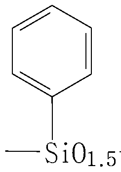
- the monomer units of the second type for the base polymer material can have a chemical composition of:
- the monomer units of the second type provide transparency at 193nm to tune the absorption property of the polymer.
- the monomer units of the second type also provides adhesion to the undercoat organic planarization layer and/or the overcoat photoresist.
- the monomer units of the third type for the base polymer material can have a chemical com osition of:
- the monomer units of the third type provide absorption of 193nm ultraviolet light in the polymer layer 90 so that the polymer layer can be used as an ARC material.
- the monomer units of the first type can collectively have a mole percentage greater than 70 % of the base polymer material. In one embodiment, the monomer units of the first type can collectively have a mole percentage in a range from 75 % to 95 % of the base polymer material. In another embodiment, the monomer units of the first type can have a mole percentage in a range from 80 % to 94 % of the base polymer material.
- the monomer units of the second type can collectively have a mole percentage in a range from 0.1 % to 15 % of the base polymer material. In one embodiment, the monomer units of the second type can have a mole percentage in a range from 0.2 % to 10 % of the total weight of the base polymer material. [0027] The monomer units of the third type can collectively have a mole percentage in a range from 1 % to 15 % of the base polymer material. In one embodiment, the monomer units of the third type can have a mole percentage in a range from 2 % to 12 % of the base polymer material.
- the boron silicate polymer material contains an acid labile group that causes the SiARC material of the polymer layer 90 to change water contact angle after lithographic exposure.
- a boron silicate polymer material is a polymer material that includes silicates and boron.
- the ratio of the number of silicon atoms to the number of boron atoms in the boron silicate polymer material can be in a range from 1:2 to 2: 1, although lesser and greater ratios can also be employed.
- An example of a boron silicate polymer is disclosed in U.S. Patent Application Publication No. 2013/0005150 Al.
- the boron silicate polymer material includes monomer units of a plurality of types.
- the boron silicate polymer is a polymeric surfactant.
- the monomer units of the plurality of types can include monomers of a first type, monomers of a second type, and monomers of a third type.
- the monomer units of the first type can include a boron atom.
- the monomer units of the second type and the monomer unit of the third type can include a silicon atom.
- the boron silicate polymer material can consist of the monomer units of the first, second, and third types.
- the monomer units of the first type for the boron silicate polymer material can have a chemical composition of:
- the monomer units of the second type for the boron silicate polymer material can have a chemical composition of:
- the monomer units of the third type for the boron silicate polymer material can have a chemical composition of:
- the monomer units of the first type can collectively have a mole percentage greater than 35 % of the boron silicate polymer material. In one embodiment, the monomer units of the first type can collectively have a mole percentage in a range from 40 % to 70 % of the boron silicate polymer material. In another embodiment, the monomer units of the first type can have a mole percentage in a range from 45 % to 60 % of the boron silicate polymer material. In one embodiment, the monomer units of the first type can collectively have a mole percentage not less than 50 % of the boron silicate polymer material.
- the monomer units of the second type can collectively have a mole percentage in a range from 12.5 % to 35 % of the boron silicate polymer material. In one embodiment, the monomer units of the second type can have a mole percentage in a range from 20 % to 30 % of the boron silicate polymer material. [0035] The monomer units of the third type can collectively have a mole percentage in a range from 12.5 % to 35 % of the boron silicate polymer material. In one embodiment, the monomer units of the third type can have a mole percentage in a range from 20 % to 30% of the boron silicate polymer material.
- the boron silicate polymer material is mixed with the base polymer material such that the ratio of the weight of the boron silicate polymer material to the weight of the base polymer material is in a range from 0.5: 100 to 20: 100. In one embodiment, the ratio of the weight of the boron silicate polymer material to the weight of the base polymer material is in a range from 1 : 100 to 10: 100. In another embodiment, the ratio of the weight of the boron silicate polymer material to the weight of the base polymer material is in a range from 2: 100 to 5: 100.
- the polymer layer 90 can be applied to the top surface of the substrate 10, for example, by spin coating.
- the boron silicate polymer material contains acid labile group having tendency to form insoluble material during the conventional stripping process.
- the base polymer material forms a silicon-based polymeric matrix in which the boron silicate polymer material is embedded. Due to strong molecular interaction, it is difficult to break up the boron silicate polymer material during the wet etch process known in the art. This property causes defects to be left on a substrate upon attempts to remove the NTD SiARC material from the substrate when conventional etch processes are employed.
- the polymer layer 90 can be removed from above the top surface of the substrate 10 by a wet etch sequence without leaving residues or defect materials on the surface of the substrate 10 according to an embodiment of the present disclosure.
- the wet etch sequence of the present disclosure is a three-step wet etch sequence, which is illustrated in FIG. 3.
- the wet etch sequence includes a first step 100 of a first wet etch employing a basic solution, a second step 200 of a second wet etch employing an acidic solution, and a third step 300 of a third wet etch employing the basic solution.
- the first wet etch can dissolve base soluble components of the polymer including silicon polymer with remaining hydroxyl group or the slow break down of the O-Si-0 or Si-R linkages with base catalyzed hydrolysis.
- the R group here represents organic moiety.
- the first etch can also dissolve any organic components which are soluble in base.
- the second wet etch can remove the main -SiO x - component due to the known dissolution of Si materials in hydrofluoric acid solutions.
- the third wet etch can then remove any residual organic and inorganic components.
- This inventive process can be applied to most of the SiARC materials known in the art including PTD SiARC's and NTD SiARC's. It is specially useful for NTD SiARC which the conventional rework process cannot fully remove the SiARC materials and leaves a lot of defects on the wafer.
- this inventive process was successfully used to remove the SiARC materials having a bas polymer containing one or more monomer units having structures selected from (I) to ( ⁇ ).
- this inventive process was successfully used to remove the NTD SiARC materials having a base polymer and a polymer capable of modifying the surface property of the base polymer including a monomer unit having a structure of IV.
- this inventive process was successfully used to remove the NTD SiARC materials having a base polymer and a boron silicate polymer.
- the first wet etch can be employed to break up the boron silicate polymer, and the second wet etch can remove the base polymer material, and the third wet etch can remove the residual boron silicate polymer and other residual materials.
- the SiARC material of the polymer layer 90, which contains the boron silicate polymer, can be removed from the substrate employing the etch sequence, and the substrate 10 can be reused for monitoring purposes.
- the embedded boron silicate polymer material in the polymer layer 90 is removed selectively to the base polymer material in the polymer layer 90 by the first wet etch that employs the first basic solution.
- the first basic solution of the first wet etch hydrolyzes and dissolves most of the boron silicate polymer material.
- the embedded boron silicate polymer material may be removed selectively to the base polymer material by the first wet etch, i.e., without removing the base polymer material in the silicon-based polymeric matrix.
- the duration of the first wet etch depends on the thickness of the polymer layer 90. For a thickness of 50 nm for the polymer layer 90, the duration of the first wet etch can be in a range from 2 minutes to 30 minutes, although lesser and greater durations can also be employed.
- the basic solution used in the first wet etch may contain amines or quaternary ammonium hydroxides.
- Aqueous ammonium hydroxides are preferred.
- Examples of quaternary ammonium hydroxides which can be used in accordance with the process of the present invention include tetramethylammonium hydroxide (TMAH), tetraethylammonium hydroxide, tetrapropylammonium hydroxide, trimethylhydroxyethylammonium hydroxide,
- 0.263N TMAH aqueous solution was used as the first wet etch solution.
- Organic solvents are useful in dissolving and wetting the organic components of the SiARC materials, therefore can be added in with quaternary ammonium hydroxide to form the first wet etch solution.
- the first basic solution includes at least N-methyl-2-pyrrolidone, propylene glycol, and tetramethylammonium hydroxide.
- the weight percentage of N-methyl-2- pyrrolidone can be in a range from 50 % to 90 %. In one embodiment, the weight percentage of N-methyl-2-pyrrolidone can be in a range from 67 % to 77 %.
- the weight percentage of propylene glycol can be in a range from 10 % to 40 %. In one embodiment, the weight percentage of propylene glycol can be in a range from 21 % to 31 %.
- the weight percentage of tetramethylammonium hydroxide can be in a range from 1 % to 5 %.
- the weight percentage of tetramethylammonium hydroxide can be in a range from 1.2 % to 2.7 %.
- the first basic solution can include water. If water is present in the first basic solution, the weight percentage of water can be in a range from 0.1 % to 2 %.
- the base polymer material of the silicon-based polymeric matrix in the polymer layer 90 is removed by the second wet etch that employs the acidic solution.
- An acid that can effectively dissolve the monomer units of the first type, i.e., SiO(OH) 2 can be selected for the acidic solution.
- the second wet etch is not effective in removing the boron silicate polymer material.
- more than 90 % of the material of the base polymer material is removed by the second wet etch.
- more than 99 % of the material of the base polymer material is removed by the second wet etch.
- the acidic solution can easily penetrates into the bulk of the SiARC material because of microcavities formed by removal of the boron silicate polymer.
- the acidic solution dissolves the base polymer material.
- the duration of the second wet etch depends on the thickness of the polymer layer 90. For a thickness of 50 nm for the polymer layer 90, the duration of the second wet etch can be in a range from 2 minutes to 20 minutes, although lesser and greater durations can also be employed.
- the acidic solution includes diluted hydrofluoric acid.
- the diluted hydrofluoric acid includes hydrofluoric acid at a weight percentage in a range from 0.1 % to 2.0 %.
- the diluted hydrofluoric acid includes hydrofluoric acid at a weight percentage in a range from 0.2 % to 1.0 %.
- the acidic solution can consist essentially of the diluted hydrofluoric acid.
- the second basic solution treatment removes any remaining boron silicate polymer and any residual base polymer.
- the duration of the third wet etch depends on the thickness of the polymer layer 90. For a thickness of 50 nm for the polymer layer 90, the duration of the third wet etch can be in a range from 2 minutes to 30 minutes, although lesser and greater durations can also be employed.
- the second basic solution includes at least N-methyl-2-pyrrolidone, propylene glycol, and tetramethylammonium hydroxide.
- the weight percentage of N-methyl-2- pyrrolidone can be in a range from 50 % to 90 %. In one embodiment, the weight percentage of N-methyl-2-pyrrolidone can be in a range from 67 % to 77 %.
- the weight percentage of propylene glycol can be in a range from 10 % to 40 %. In one embodiment, the weight percentage of propylene glycol can be in a range from 21 % to 31 %.
- the weight percentage of tetramethylammonium hydroxide can be in a range from 1 % to 5 %.
- the weight percentage of tetramethylammonium hydroxide can be in a range from 1.2 % to 2.7 %.
- the second basic solution can include water. If water is present in the second basic solution, the weight percentage of water can be in a range from 0.1 % to 2 %.
- the second basic solution can have any composition that can be employed for the first basic solution. The composition of the second basic solution can be the same as, or can be different from, the composition of the first basic solution.
- the wet etch process sequence can completely eliminate the SiARC material layer from the substrate 10.
- the wet etch process sequence has been demonstrated to provide superior results compared to other wet etch process sequences.
- a comparative exemplary wet etch sequence which includes a first wet etch employing a combination of a sulfuric acid and hydrofluoric acid, a second wet etch employing a combination of deionized water, hydrogen peroxide, and ammonium hydroxide, and a third wet etch employing dilute hydrofluoric acid, was shown to be insufficient to remove a SiARC material layer completely without residual polymers.
Landscapes
- Physics & Mathematics (AREA)
- General Physics & Mathematics (AREA)
- Engineering & Computer Science (AREA)
- Architecture (AREA)
- Structural Engineering (AREA)
- Chemical & Material Sciences (AREA)
- Cleaning Or Drying Semiconductors (AREA)
- Chemical Kinetics & Catalysis (AREA)
- General Chemical & Material Sciences (AREA)
- Materials For Photolithography (AREA)
- Photosensitive Polymer And Photoresist Processing (AREA)
- Life Sciences & Earth Sciences (AREA)
- Materials Engineering (AREA)
- Wood Science & Technology (AREA)
- Organic Chemistry (AREA)
- Paints Or Removers (AREA)
- Weting (AREA)
Abstract
Description




Claims


Priority Applications (3)
| Application Number | Priority Date | Filing Date | Title |
|---|---|---|---|
| DE112014001478.8T DE112014001478B4 (en) | 2013-03-15 | 2014-02-17 | Wet stripping process for an anti-reflective coating layer |
| KR1020157015655A KR102184205B1 (en) | 2013-03-15 | 2014-02-17 | Wet strip process for an antireflective coating layer |
| JP2016500278A JP6172372B2 (en) | 2013-03-15 | 2014-02-17 | Wet peeling method of antireflection film layer |
Applications Claiming Priority (2)
| Application Number | Priority Date | Filing Date | Title |
|---|---|---|---|
| US13/833,317 | 2013-03-15 | ||
| US13/833,317 US9460934B2 (en) | 2013-03-15 | 2013-03-15 | Wet strip process for an antireflective coating layer |
Publications (1)
| Publication Number | Publication Date |
|---|---|
| WO2014149286A1 true WO2014149286A1 (en) | 2014-09-25 |
Family
ID=51528999
Family Applications (1)
| Application Number | Title | Priority Date | Filing Date |
|---|---|---|---|
| PCT/US2014/016700 Ceased WO2014149286A1 (en) | 2013-03-15 | 2014-02-17 | Wet strip process for an antireflective coating layer |
Country Status (6)
| Country | Link |
|---|---|
| US (1) | US9460934B2 (en) |
| JP (1) | JP6172372B2 (en) |
| KR (1) | KR102184205B1 (en) |
| DE (1) | DE112014001478B4 (en) |
| TW (1) | TWI600079B (en) |
| WO (1) | WO2014149286A1 (en) |
Cited By (2)
| Publication number | Priority date | Publication date | Assignee | Title |
|---|---|---|---|---|
| WO2017151383A1 (en) * | 2016-02-29 | 2017-09-08 | Tokyo Electron Limited | Selective siarc removal |
| CN107577120A (en) * | 2016-07-04 | 2018-01-12 | 东友精细化工有限公司 | Anticorrosive additive stripping liquid controlling composition, display base plate and its manufacture method |
Families Citing this family (9)
| Publication number | Priority date | Publication date | Assignee | Title |
|---|---|---|---|---|
| US9782804B1 (en) * | 2012-01-26 | 2017-10-10 | Tgs Solutions, Llc | Method for passivating substrate surfaces |
| US9508560B1 (en) | 2015-06-18 | 2016-11-29 | International Business Machines Corporation | SiARC removal with plasma etch and fluorinated wet chemical solution combination |
| JP6761166B2 (en) * | 2015-07-23 | 2020-09-23 | セントラル硝子株式会社 | Wet etching method and etching solution |
| JPWO2017169487A1 (en) * | 2016-03-30 | 2019-02-07 | Jsr株式会社 | Film forming material for resist process and pattern forming method |
| US10114288B2 (en) * | 2016-09-01 | 2018-10-30 | Rohm And Haas Electronic Materials Llc | Silicon-containing underlayers |
| US10007184B2 (en) | 2016-09-01 | 2018-06-26 | Rohm And Haas Electronic Materials Llc | Silicon-containing underlayers |
| US10049876B1 (en) | 2017-02-13 | 2018-08-14 | International Business Machines Corporation | Removal of trilayer resist without damage to underlying structure |
| JP7209556B2 (en) * | 2019-02-05 | 2023-01-20 | 東京エレクトロン株式会社 | Substrate processing method and substrate processing apparatus |
| WO2023055653A1 (en) * | 2021-09-30 | 2023-04-06 | Entegris, Inc. | Articles having removable coatings and related methods |
Citations (4)
| Publication number | Priority date | Publication date | Assignee | Title |
|---|---|---|---|---|
| US5911836A (en) * | 1996-02-05 | 1999-06-15 | Mitsubishi Gas Chemical Company, Inc. | Method of producing semiconductor device and rinse for cleaning semiconductor device |
| US6103637A (en) * | 1998-03-13 | 2000-08-15 | Micron Technology, Inc. | Method for selective etching of antireflective coatings |
| US20050176602A1 (en) * | 2002-06-07 | 2005-08-11 | Hsu Chien-Pin S. | Microelectronic cleaning and arc remover compositions |
| US20080138997A1 (en) * | 2006-12-08 | 2008-06-12 | Applied Materials, Inc. | Two step etching of a bottom anti-reflective coating layer in dual damascene application |
Family Cites Families (15)
| Publication number | Priority date | Publication date | Assignee | Title |
|---|---|---|---|---|
| US6319835B1 (en) | 2000-02-25 | 2001-11-20 | Shipley Company, L.L.C. | Stripping method |
| EP1386350A1 (en) * | 2001-04-27 | 2004-02-04 | Koninklijke Philips Electronics N.V. | Method of wet etching an inorganic antireflection layer |
| US6749760B2 (en) | 2001-10-26 | 2004-06-15 | Intel Corporation | Etchant formulation for selectively removing thin films in the presence of copper, tin, and lead |
| KR20050042051A (en) * | 2001-11-02 | 2005-05-04 | 미츠비시 가스 가가쿠 가부시키가이샤 | Method for releasing resist |
| US7393819B2 (en) | 2002-07-08 | 2008-07-01 | Mallinckrodt Baker, Inc. | Ammonia-free alkaline microelectronic cleaning compositions with improved substrate compatibility |
| US6683008B1 (en) | 2002-11-19 | 2004-01-27 | International Business Machines Corporation | Process of removing ion-implanted photoresist from a workpiece |
| US7700533B2 (en) | 2005-06-23 | 2010-04-20 | Air Products And Chemicals, Inc. | Composition for removal of residue comprising cationic salts and methods using same |
| US20080096785A1 (en) * | 2006-10-19 | 2008-04-24 | Air Products And Chemicals, Inc. | Stripper Containing an Acetal or Ketal for Removing Post-Etched Photo-Resist, Etch Polymer and Residue |
| JP4499751B2 (en) * | 2006-11-21 | 2010-07-07 | エア プロダクツ アンド ケミカルズ インコーポレイテッド | Formulation for removing photoresist, etch residue and BARC and method comprising the same |
| US8026201B2 (en) * | 2007-01-03 | 2011-09-27 | Az Electronic Materials Usa Corp. | Stripper for coating layer |
| US8614053B2 (en) | 2009-03-27 | 2013-12-24 | Eastman Chemical Company | Processess and compositions for removing substances from substrates |
| US20110076623A1 (en) * | 2009-09-29 | 2011-03-31 | Tokyo Electron Limited | Method for reworking silicon-containing arc layers on a substrate |
| US8288271B2 (en) * | 2009-11-02 | 2012-10-16 | International Business Machines Corporation | Method for reworking antireflective coating over semiconductor substrate |
| JP5404459B2 (en) * | 2010-02-08 | 2014-01-29 | 東京応化工業株式会社 | Lithographic cleaning liquid and wiring forming method |
| US8323871B2 (en) * | 2010-02-24 | 2012-12-04 | International Business Machines Corporation | Antireflective hardmask composition and a method of preparing a patterned material using same |
-
2013
- 2013-03-15 US US13/833,317 patent/US9460934B2/en not_active Expired - Fee Related
-
2014
- 2014-02-17 KR KR1020157015655A patent/KR102184205B1/en active Active
- 2014-02-17 JP JP2016500278A patent/JP6172372B2/en active Active
- 2014-02-17 WO PCT/US2014/016700 patent/WO2014149286A1/en not_active Ceased
- 2014-02-17 DE DE112014001478.8T patent/DE112014001478B4/en not_active Expired - Fee Related
- 2014-03-12 TW TW103108803A patent/TWI600079B/en not_active IP Right Cessation
Patent Citations (4)
| Publication number | Priority date | Publication date | Assignee | Title |
|---|---|---|---|---|
| US5911836A (en) * | 1996-02-05 | 1999-06-15 | Mitsubishi Gas Chemical Company, Inc. | Method of producing semiconductor device and rinse for cleaning semiconductor device |
| US6103637A (en) * | 1998-03-13 | 2000-08-15 | Micron Technology, Inc. | Method for selective etching of antireflective coatings |
| US20050176602A1 (en) * | 2002-06-07 | 2005-08-11 | Hsu Chien-Pin S. | Microelectronic cleaning and arc remover compositions |
| US20080138997A1 (en) * | 2006-12-08 | 2008-06-12 | Applied Materials, Inc. | Two step etching of a bottom anti-reflective coating layer in dual damascene application |
Non-Patent Citations (1)
| Title |
|---|
| KOVACS, GREGORY T. A. ET AL.: "Bulk Micromachining of Silicon", PROCEEDINGS OF THE IEEE, vol. 86, no. 8, 1998, pages 1536 - 1551, XP011044069 * |
Cited By (4)
| Publication number | Priority date | Publication date | Assignee | Title |
|---|---|---|---|---|
| WO2017151383A1 (en) * | 2016-02-29 | 2017-09-08 | Tokyo Electron Limited | Selective siarc removal |
| US10115591B2 (en) | 2016-02-29 | 2018-10-30 | Tokyo Electron Limited | Selective SiARC removal |
| CN107577120A (en) * | 2016-07-04 | 2018-01-12 | 东友精细化工有限公司 | Anticorrosive additive stripping liquid controlling composition, display base plate and its manufacture method |
| CN107577120B (en) * | 2016-07-04 | 2022-03-25 | 东友精细化工有限公司 | Resist stripping liquid composition, display substrate and manufacturing method thereof |
Also Published As
| Publication number | Publication date |
|---|---|
| KR102184205B1 (en) | 2020-11-27 |
| US9460934B2 (en) | 2016-10-04 |
| JP2016513884A (en) | 2016-05-16 |
| TW201507016A (en) | 2015-02-16 |
| DE112014001478T5 (en) | 2015-12-17 |
| TWI600079B (en) | 2017-09-21 |
| US20140273501A1 (en) | 2014-09-18 |
| KR20160002663A (en) | 2016-01-08 |
| DE112014001478B4 (en) | 2017-08-31 |
| JP6172372B2 (en) | 2017-08-02 |
Similar Documents
| Publication | Publication Date | Title |
|---|---|---|
| US9460934B2 (en) | Wet strip process for an antireflective coating layer | |
| KR101715965B1 (en) | Composition for forming a silicon-containing resist underlayer film and patterning process using the same | |
| KR101801437B1 (en) | Composition for forming titanium-containing resist underlayer film and patterning process | |
| KR101735856B1 (en) | Composition for forming resist underlayer film and patterning process using the same | |
| KR101902046B1 (en) | Metal-oxide films from small molecules for lithographic applications | |
| KR101570251B1 (en) | Composition for forming a silicon-containing antireflection film, substrate having the silicon-containing antireflection film from the composition and patterning process using the same | |
| US8836082B2 (en) | Reversal lithography approach by selective deposition of nanoparticles | |
| US9249013B2 (en) | Silicon hardmask layer for directed self-assembly | |
| KR101724792B1 (en) | Composition for forming titanium-containing resist underlayer film and patterning process | |
| KR102129860B1 (en) | Photoresist pattern trimming methods | |
| KR101901564B1 (en) | Composition for forming tungsten oxide film and method for producing tungsten oxide film using same | |
| KR101776365B1 (en) | Composition for forming resist underlayer film and patterning process | |
| CN102439523B (en) | Method and materials for double patterning | |
| KR101822223B1 (en) | Composition for forming titanium-containing resist underlayer film and patterning process | |
| JP7747825B2 (en) | Aqueous solution for manufacturing electronic equipment, method for manufacturing resist pattern, and method for manufacturing device | |
| CN101872126B (en) | wet soluble lithography | |
| KR101648612B1 (en) | Patterning process | |
| JP3974295B2 (en) | Pattern formation method | |
| KR20180118636A (en) | Method of planarizing a semiconductor substrate using a silicon-containing composition | |
| US9671694B1 (en) | Wet strippable gap fill materials | |
| JP6738050B2 (en) | Aqueous solution for coating resist pattern and pattern forming method using the same | |
| KR20180053309A (en) | A composition for coating a resist pattern comprising a vinyl group or a (meth) acryloxy group-containing polysiloxane | |
| KR20190059893A (en) | Method for preparing composition for applying resist pattern using solvent substitution method | |
| KR20140106108A (en) | Method of forming thin layer patterns in semiconductor device | |
| CN117693718A (en) | Electronic device manufacturing aqueous solution, method of manufacturing resist pattern, and method of manufacturing device |
Legal Events
| Date | Code | Title | Description |
|---|---|---|---|
| 121 | Ep: the epo has been informed by wipo that ep was designated in this application |
Ref document number: 14771029 Country of ref document: EP Kind code of ref document: A1 |
|
| ENP | Entry into the national phase |
Ref document number: 20157015655 Country of ref document: KR Kind code of ref document: A |
|
| ENP | Entry into the national phase |
Ref document number: 2016500278 Country of ref document: JP Kind code of ref document: A |
|
| WWE | Wipo information: entry into national phase |
Ref document number: 112014001478 Country of ref document: DE Ref document number: 1120140014788 Country of ref document: DE |
|
| 122 | Ep: pct application non-entry in european phase |
Ref document number: 14771029 Country of ref document: EP Kind code of ref document: A1 |