WO2014109225A1 - 表示装置 - Google Patents
表示装置 Download PDFInfo
- Publication number
- WO2014109225A1 WO2014109225A1 PCT/JP2013/084517 JP2013084517W WO2014109225A1 WO 2014109225 A1 WO2014109225 A1 WO 2014109225A1 JP 2013084517 W JP2013084517 W JP 2013084517W WO 2014109225 A1 WO2014109225 A1 WO 2014109225A1
- Authority
- WO
- WIPO (PCT)
- Prior art keywords
- lens
- lens member
- pixel
- display panel
- light
- Prior art date
- Legal status (The legal status is an assumption and is not a legal conclusion. Google has not performed a legal analysis and makes no representation as to the accuracy of the status listed.)
- Ceased
Links
Images





Classifications
-
- G—PHYSICS
- G02—OPTICS
- G02B—OPTICAL ELEMENTS, SYSTEMS OR APPARATUS
- G02B26/00—Optical devices or arrangements for the control of light using movable or deformable optical elements
- G02B26/08—Optical devices or arrangements for the control of light using movable or deformable optical elements for controlling the direction of light
- G02B26/0875—Optical devices or arrangements for the control of light using movable or deformable optical elements for controlling the direction of light by means of one or more refracting elements
-
- G—PHYSICS
- G02—OPTICS
- G02B—OPTICAL ELEMENTS, SYSTEMS OR APPARATUS
- G02B26/00—Optical devices or arrangements for the control of light using movable or deformable optical elements
- G02B26/004—Optical devices or arrangements for the control of light using movable or deformable optical elements based on a displacement or a deformation of a fluid
- G02B26/005—Optical devices or arrangements for the control of light using movable or deformable optical elements based on a displacement or a deformation of a fluid based on electrowetting
-
- G—PHYSICS
- G02—OPTICS
- G02B—OPTICAL ELEMENTS, SYSTEMS OR APPARATUS
- G02B3/00—Simple or compound lenses
- G02B3/0006—Arrays
- G02B3/0037—Arrays characterized by the distribution or form of lenses
-
- G—PHYSICS
- G02—OPTICS
- G02B—OPTICAL ELEMENTS, SYSTEMS OR APPARATUS
- G02B3/00—Simple or compound lenses
- G02B3/0006—Arrays
- G02B3/0037—Arrays characterized by the distribution or form of lenses
- G02B3/0062—Stacked lens arrays, i.e. refractive surfaces arranged in at least two planes, without structurally separate optical elements in-between
- G02B3/0068—Stacked lens arrays, i.e. refractive surfaces arranged in at least two planes, without structurally separate optical elements in-between arranged in a single integral body or plate, e.g. laminates or hybrid structures with other optical elements
Definitions
- the present invention relates to a display device, and more particularly, to a display device including an optical path changing device that changes a path of light emitted from pixels formed on a display panel.
- the aperture area of the pixel becomes smaller.
- the aperture area of the pixel becomes small, it becomes difficult to transmit the backlight light. Therefore, it is necessary to brighten the backlight light. Therefore, the liquid crystal display device has a problem that power consumption increases as the definition becomes higher.
- An object of the present invention is to provide a display device capable of increasing the apparent number of pixels.
- the display device includes a display panel and an optical path changing device.
- the display panel includes a plurality of pixels formed side by side in a predetermined direction.
- the optical path changing device is arranged closer to the viewer than the display panel, and changes the path of light emitted from the pixels.
- the optical path changing device includes a first lens member, a second lens member, and an emission direction control device.
- a plurality of second lens members are arranged side by side in a predetermined direction on the display panel side of the first lens member.
- the emission direction control device changes the direction in which the pixel light incident on the second lens member is emitted from the second lens member.
- the first lens member includes an inner lens surface and a pair of outer lens surfaces.
- a plurality of inner lens surfaces are formed side by side in a predetermined direction on the display panel side.
- the pair of outer lens surfaces are formed side by side in a predetermined direction, and overlap the inner lens surface when the display panel is viewed from the front.
- the pixel light incident on the inner lens surface is emitted from one of the pair of outer lens surfaces in accordance with the direction in which the pixel light incident on the second lens member is emitted from the second lens member.
- the apparent number of pixels can be increased.
- FIG. 5 It is a top view which shows the optical path changing apparatus with which the display apparatus shown in FIG. 5 is provided. It is a schematic diagram which shows the path
- the display device includes a display panel and an optical path changing device.
- the display panel includes a plurality of pixels formed side by side in a predetermined direction.
- the optical path changing device is arranged closer to the viewer than the display panel, and changes the path of light emitted from the pixels.
- the optical path changing device includes a first lens member, a second lens member, and an emission direction control device.
- a plurality of second lens members are arranged side by side in a predetermined direction on the display panel side of the first lens member.
- the emission direction control device changes the direction in which the pixel light incident on the second lens member is emitted from the second lens member.
- the first lens member includes an inner lens surface and a pair of outer lens surfaces.
- a plurality of inner lens surfaces are formed side by side in a predetermined direction on the display panel side.
- the pair of outer lens surfaces are formed side by side in a predetermined direction, and overlap the inner lens surface when the display panel is viewed from the front.
- the pixel light incident on the inner lens surface is emitted from one of the pair of outer lens surfaces in accordance with the direction in which the pixel light incident on the second lens member is emitted from the second lens member.
- the pixel light incident on the inner lens surface is incident on the pair of outer lens surfaces according to the direction in which the pixel light incident on the second lens member exits from the second lens member. It emits from either. Therefore, according to the above configuration, the apparent number of pixels can be increased in a predetermined direction.
- the second lens member in the first configuration, is rotatably arranged between the first position and a second position different from the first position.
- the pixel light is condensed in different directions when the second lens is at the first position and when the second lens is at the second position.
- the direction in which the pixel light incident on the second lens member is emitted from the second lens member can be switched.
- the second lens member in the first configuration, is disposed so as to be capable of reciprocating between the first position and a second position different from the first position.
- the pixel light is condensed in different directions when the second lens is at the first position and when the second lens is at the second position.
- the direction in which the pixel light incident on the second lens member is emitted from the second lens member can be switched.
- a fourth configuration is the first configuration, wherein the second lens member includes a substrate, a groove, a water repellent dielectric film, an electrode, an oil film, and a liquid.
- the substrate is disposed to face the first lens member.
- a plurality of grooves are formed side by side in a predetermined direction on the surface of the substrate facing the first lens member.
- the water repellent dielectric film is disposed on the inner surface of the groove.
- the electrode is disposed on each of the pair of walls of the groove and covered with a water-repellent dielectric film.
- the oil film is disposed in contact with the water-repellent dielectric film and is accommodated in the groove.
- the liquid is arranged separately from the oil film and covers the oil film.
- the emission direction control device changes the voltage applied to the first electrode.
- the interface between the oil film and the liquid is deformed by changing the voltage applied to the first electrode. Therefore, it is possible to switch the direction in which the pixel light incident on the second lens member is emitted from the second lens member.
- the fifth configuration is any one of the first to fourth configurations, wherein the pixel emits light of different colors and includes a plurality of sub-pixels formed side by side in the predetermined direction.
- Each of the pair of outer lens surfaces includes a first outer lens surface corresponding to each sub-pixel.
- FIG. 1 shows a display device 10 according to a first embodiment of the present invention.
- the display device 10 includes a display panel 12 and an optical path changing device 14.
- the display panel 12 includes a plurality of pixels 16 formed side by side in the left-right direction (the horizontal direction of the display panel 12).
- Each pixel 16 includes a plurality of sub-pixels 16R, 16G, and 16B.
- the plurality of sub-pixels 16R, 16G, and 16B are arranged side by side in the direction in which the plurality of pixels 16 are arranged.
- the plurality of subpixels 16R, 16G, and 16B emit light of different colors. In the present embodiment, the sub-pixel 16R emits red light, the sub-pixel 16G emits green light, and the sub-pixel 16B emits blue light.
- the display panel 12 is not particularly limited.
- the display panel 12 may be, for example, a liquid crystal panel, an organic EL panel, or a plasma display panel.
- the display panel 12 is a liquid crystal panel
- the display device 10 includes a backlight (not shown). The light from the backlight passes through the pixels of the liquid crystal panel, so that the pixels emit light.
- the optical path changing device 14 is disposed closer to the viewer than the display panel 12 and changes the path (optical path) of light emitted from the pixels 16.
- the optical path changing device 14 includes a first lens member 18, a second lens member 20, and an emission direction control device 22 (see FIG. 2).
- the first lens member 18 includes an inner lens surface 24 and a pair of outer lens surfaces 26R and 26L.
- a plurality of inner lens surfaces 24 are formed side by side in the left-right direction on the display panel 12 side.
- the plurality of inner lens surfaces 24 are concave lens surfaces that are concave on the display panel 12 side.
- the width center C1 of the pixel 16 in the left-right direction is located on the boundary B1 between the two inner lens surfaces 24 adjacent in the left-right direction.
- the width center C2 in the left-right direction of the sub-pixel 16G is located on the boundary B1.
- the length of the inner lens surface 24 in the left-right direction is the same as the pixel pitch.
- the pair of outer lens surfaces 26R and 26L are formed side by side in the left-right direction on the viewer side.
- the pair of outer lens surfaces 26R and 26L overlap each of the plurality of inner lens surfaces 24. That is, in the first lens member 18, the outer lens surface 26R and the outer lens surface 26L are alternately formed in the left-right direction on the viewer side.
- the width center C3 of the inner lens surface 24 in the left-right direction is located on the boundary B2 between the pair of outer lens surfaces 26R and 26L that overlap the one inner lens surface 24 when the display panel 12 is viewed from the front.
- An outer lens surface 26R that overlaps one of the two inner lens surfaces 24 that are adjacent in the left-right direction when the display panel 12 is viewed from the front, and two inner lenses that are adjacent in the left-right direction when the display panel 12 is viewed from the front.
- the boundary with the outer lens surface 26L overlapping the other of the surface 24 is located on the boundary B1.
- the outer lens surface 26R includes first outer lens surfaces 28RR, 28GR, and 28BR corresponding to the sub-pixels 16R, 16G, and 16B.
- the plurality of first outer lens surfaces 28RR, 28GR, and 28BR are formed side by side in the left-right direction.
- the order in which the plurality of first outer lens surfaces 28RR, 28GR, 28BR are arranged in the left-right direction is the same as the order in which the plurality of sub-pixels 16R, 16G, 16B are arranged in the left-right direction.
- the plurality of first outer lens surfaces 28RR, 28GR, and 28BR are concave lens surfaces that are concave on the viewer side.
- the outer lens surface 26L includes first outer lens surfaces 28RL, 28GL, and 28BL corresponding to the sub-pixels 16R, 16G, and 16B.
- the plurality of first outer lens surfaces 28RL, 28GL, and 28BL are formed side by side in the left-right direction.
- the order in which the plurality of first outer lens surfaces 28RL, 28GL, 28BL are arranged in the left-right direction is the same as the order in which the plurality of sub-pixels 16R, 16G, 16B are arranged in the left-right direction.
- the plurality of first outer lens surfaces 28RL, 28GL, and 28BL are concave lens surfaces that are concave on the viewer side.
- a plurality of second lens members 20 are arranged side by side in the left-right direction on the display panel 12 side of the first lens member 18.
- the second lens member 20 is disposed for each pixel 16. That is, the same number of second lens members 20 as the number of pixels 16 arranged in the left-right direction are arranged.
- the width center C4 in the left-right direction of the second lens member 20 overlaps the width center C1 in the left-right direction of the pixel 16 and is a boundary between two inner lens surfaces 24 adjacent in the left-right direction. Located on B1.
- the second lens member 20 is a plate-like member extending in a predetermined cross section.
- the cross section of the second lens member 20 has a symmetrical shape with respect to the reference line L1 extending in the left-right direction.
- the thickness of the second lens member 20 decreases from one to the other in the left-right direction.
- the two lens surfaces (an incident surface on which light is incident and an exit surface on which light is emitted) of the second lens member 20 are convex lens surfaces, respectively. Therefore, the light incident on the second lens member 20 is collected in a specific direction (the thicker end portion side of the second lens member 20).
- the length of the second lens member 20 in the left-right direction is the same as the length of the inner lens surface 24 in the left-right direction.
- the second lens member 20 is arranged in the same direction. That is, in the two second lens members 20 that are adjacent in the left-right direction, the thinner end of the other second lens member 20 is positioned next to the thicker end of one second lens member 20. .
- the emission direction control device 22 includes a motor 34.
- the motor 34 is driven by a drive circuit (not shown).
- the driving force of the motor 34 is transmitted to a shaft 30 ⁇ / b> A provided at one end of the second lens member 20 in the length direction.
- the shaft 30B provided at the other end in the length direction of the second lens member 20 is rotatably supported by the support member 32 disposed on the surface of the display panel 12 on the viewer side.
- the left inner lens surface 24 of the two inner lens surfaces 24 that overlaps the second lens member 20 when the display panel 12 is viewed from the front. Exit toward.
- the light emitted from the sub-pixel 16R is incident on the inner lens surface 24 and then exits from the first outer lens surface 28RR that overlaps the inner lens surface 24 when the display panel 12 is viewed from the front.
- the light emitted from the sub-pixel 16G When the light emitted from the sub-pixel 16G is incident on the second lens member 20, the light is emitted toward the left inner lens surface 24.
- the light emitted from the sub-pixel 16G enters the inner lens surface 24, and then exits from the first outer lens surface 28GR that overlaps the inner lens surface 24 when the display panel 12 is viewed from the front.
- the light emitted from the sub-pixel 16B When the light emitted from the sub-pixel 16B is incident on the second lens member 20, it is emitted toward the inner lens surface 24 on the left side.
- the light emitted from the sub-pixel 16B enters the inner lens surface 24, and then exits from the first outer lens surface 28BR that overlaps the inner lens surface 24 when the display panel 12 is viewed from the front.
- the second lens member 20 rotates around the central axis of the shaft 30A. Thereby, the 2nd lens member 20 will be in the state shown to FIG. 3B.
- the second lens member 20 is half-rotated as compared to the state shown in FIG. 3A.
- the path of light emitted from each of the sub-pixels 16R, 16G, and 16B is as follows.
- the right inner lens surface 24 of the two inner lens surfaces 24 that overlaps the second lens member 20 when the display panel 12 is viewed from the front. Exit toward.
- the light emitted from the sub-pixel 16R is incident on the inner lens surface 24 and then exits from the first outer lens surface 28RL that overlaps the inner lens surface 24 when the display panel 12 is viewed from the front.
- the light emitted from the sub-pixel 16G When the light emitted from the sub-pixel 16G is incident on the second lens member 20, it is emitted toward the inner lens surface 24 on the right side.
- the light emitted from the sub-pixel 16G enters the inner lens surface 24, and then exits from the first outer lens surface 28GL that overlaps the inner lens surface 24 when the display panel 12 is viewed from the front.
- the light emitted from the sub-pixel 16B When the light emitted from the sub-pixel 16B is incident on the second lens member 20, it is emitted toward the inner lens surface 24 on the right side.
- the light emitted from the sub-pixel 16B enters the right inner lens surface 24 and then exits from the first outer lens surface 28BL that overlaps the inner lens surface 24 when the display panel 12 is viewed from the front.
- the second lens member 20 rotates, the light emitted from the sub-pixels 16R, 16G, and 16B is alternately emitted from the outer lens surface 26R and the outer lens surface 26L. Therefore, the apparent number of pixels is doubled in the left-right direction by alternately switching the image displayed on the display panel 12 between an image emitted from the outer lens surface 26R and an image emitted from the outer lens surface 26L. It is possible to show the observer the image that became.
- timing at which the second lens member 20 rotates halfway and the timing at which the image displayed on the display panel 12 is switched need to be synchronized. Further, it is necessary to synchronize the timing at which the plurality of second lens members rotate halfway.
- the display device 10 since the light emitted from the pixels 16 is not divided for each color, the occurrence of color braking can be avoided.
- FIG. 4 For example, as shown in FIG. 4, one of the two lens surfaces 21A and 21B of the second lens member 20 is positively charged and the other is negatively charged. A pair of electrodes (not shown) are arranged with the second lens member 20 in between. A repulsive force is generated between each electrode and the second lens member 20 by changing the type of charge to be charged to each electrode. The second lens member 20 is rotated by this repulsive force. In this way, the second lens member 20 may be driven.
- a display device 10A according to a second embodiment of the present invention will be described with reference to FIGS.
- an optical path changing device 14 ⁇ / b> A is employed instead of the optical path changing device 14.
- the optical path changing device 14A differs from the optical path changing device 14 in the second lens member and the emission direction control device.
- a second lens member 20 ⁇ / b> A is disposed instead of the second lens member 20.
- the second lens member 20A is a plate-like member that extends in a predetermined cross section.
- the cross section of the second lens member 20A is symmetric with respect to the reference line L2 extending in the left-right direction and symmetric with respect to the reference line L3 extending in the up-down direction.
- Each of the two lens surfaces (an incident surface on which light is incident and an output surface on which light is emitted) included in the second lens member 20A is a convex lens surface. Therefore, the light incident on the second lens member 20A is collected in a specific direction (the center side in the left-right direction of the second lens member 20A).
- the length in the left-right direction of the second lens member 20 ⁇ / b> A is twice the length in the left-right direction of the inner lens surface 24. That is, the length in the left-right direction of the second lens member 20 ⁇ / b> A is twice the length in the left-right direction of the pixel 16.
- an emission direction control device 22 ⁇ / b> A is arranged instead of the emission direction control device 22.
- the emission direction control device 22A includes a pair of charging members 40A and 40B and a spring 46.
- the charging member 40 ⁇ / b> A is attached to the pair of support members 42 and 42.
- the pair of support members 42 and 42 extend in the horizontal direction of the display panel 12 (left and right direction in FIG. 6), and connect the plurality of second lens members 20A arranged in the horizontal direction of the display panel 12.
- one support member 42 has one ends in the vertical direction (vertical direction in FIG. 6) of the display panel 12 in the plurality of second lens members 20A (one end in the longitudinal direction in the plurality of second lens members 20A).
- the other support member 42 connects the other ends in the vertical direction of the display panel 12 in the plurality of second lens members 20A (the other ends in the longitudinal direction in the plurality of second lens members 20A). To do.
- Each support member 42 is arranged to be movable in the left-right direction by a guide member 44.
- the spring 46 connects the pair of charging members 40A and 40B.
- the charging member 40A is positively charged.
- the charging member 40B can take a negatively charged state and a state in which neither the positive nor the negatively charged member is charged.
- the charged state and uncharged state of the charging member 40B are realized by, for example, a drive circuit (not shown). Specifically, for example, the charging member 40B is negatively charged by applying a negative voltage to the charging member 40B, and the charging member 40B is grounded by charging the charging member 40B to both positive and negative. Set to the state that is not.
- the charging member 40A moves in a direction approaching the charging member 40B due to the attractive force generated between the pair of charging members 40A and 40B.
- the charging member 40B is not charged positively or negatively, the charging member 40A is moved away from the charging member 40B by the biasing force of the spring 42. Thereby, each 2nd lens member 22A is reciprocated in the left-right direction.
- the light emitted from the sub-pixel 16R included in the right pixel 16 among the two pixels 16 adjacent in the left-right direction is incident on the second lens member 20A and is positioned on the boundary B3 when the display panel 12 is viewed from the front.
- the light is emitted toward the inner lens surface 24.
- the light emitted from the sub-pixel 16R is incident on the inner lens surface 24 and then exits from the first outer lens surface 28RR that overlaps the inner lens surface 24 when the display panel 12 is viewed from the front.
- the light emitted from the sub-pixel 16G included in the right pixel 16 is incident on the second lens member 20A, the light is emitted toward the inner lens surface 24 located on the boundary B3 when the display panel 12 is viewed from the front. .
- the light emitted from the sub-pixel 16G enters the inner lens surface 24, and then exits from the first outer lens surface 28GR that overlaps the inner lens surface 24 when the display panel 12 is viewed from the front.
- the light emitted from the sub-pixel 16B included in the right pixel 16 is incident on the second lens member 20A, the light is emitted toward the inner lens surface 24 located on the boundary B3 when the display panel 12 is viewed from the front. .
- the light emitted from the sub-pixel 16B enters the inner lens surface 24, and then exits from the first outer lens surface 28BR that overlaps the inner lens surface 24 when the display panel 12 is viewed from the front.
- the light emitted from the sub-pixel 16R included in the left pixel 16 among the two pixels 16 adjacent in the left-right direction is incident on the second lens member 20A and is positioned on the boundary B3 when the display panel 12 is viewed from the front.
- the light is emitted toward the inner lens surface 24.
- the light emitted from the sub-pixel 16R is incident on the inner lens surface 24 and then exits from the first outer lens surface 28RL that overlaps the inner lens surface 24 when the display panel 12 is viewed from the front.
- the light emitted from the sub-pixel 16G included in the left pixel 16 is incident on the second lens member 20A, the light is emitted toward the inner lens surface 24 located on the boundary B3 when the display panel 12 is viewed from the front. .
- the light emitted from the sub-pixel 16G enters the inner lens surface 24, and then exits from the first outer lens surface 28GL that overlaps the inner lens surface 24 when the display panel 12 is viewed from the front.
- the light emitted from the sub-pixel 16B included in the left pixel 16 is incident on the second lens member 20A, the light is emitted toward the inner lens surface 24 located on the boundary B3 when the display panel 12 is viewed from the front. .
- the light emitted from the sub-pixel 16B enters the inner lens surface 24, and then exits from the first outer lens surface 28BL that overlaps the inner lens surface 24 when the display panel 12 is viewed from the front.
- the second lens member 20A moves in the left-right direction due to the attractive force generated between the pair of charging members 40A, 40B. As a result, the second lens member 20A is in the state shown in FIG. 7B. In the state shown in FIG. 7B, the second lens member 20A is moved by one pixel in the horizontal direction compared to the state shown in FIG. 7A. Thereby, in the state shown in FIG. 7B, compared to the state shown in FIG. 7A, the two second lens members 20A are located across the boundary B3. In the state shown in FIG. 7B, the path of light emitted from each of the sub-pixels 16R, 16G, and 16B is as follows.
- the display panel 12 When the light emitted from the sub-pixel 16R included in the right pixel 16 among the two pixels 16 adjacent in the left-right direction is incident on the second lens member 20A located on the right side of the boundary B3, the display panel 12 is viewed from the front. Sometimes the light is emitted toward the inner lens surface 24 located on the right side of the inner lens surface 24 located on the boundary B3. The light emitted from the sub-pixel 16R is incident on the inner lens surface 24 and then exits from the first outer lens surface 28RL that overlaps the inner lens surface 24 when the display panel 12 is viewed from the front.
- the inner side positioned on the boundary B3 when the display panel 12 is viewed from the front.
- the light is emitted toward the inner lens surface 24 located on the right side of the lens surface 24.
- the light emitted from the sub-pixel 16B enters the inner lens surface 24, and then exits from the first outer lens surface 28BL that overlaps the inner lens surface 24 when the display panel 12 is viewed from the front.
- the display panel 12 When the light emitted from the sub-pixel 16R included in the left pixel 16 among the two pixels 16 adjacent in the left-right direction is incident on the second lens member 20A located on the left side of the boundary B3, the display panel 12 is viewed from the front. Sometimes the light is emitted toward the inner lens surface 24 located on the left side of the inner lens surface 24 located on the boundary B3. The light emitted from the sub-pixel 16R is incident on the inner lens surface 24 and then exits from the first outer lens surface 28RR that overlaps the inner lens surface 24 when the display panel 12 is viewed from the front.
- the light emitted from the sub-pixel 16G included in the left pixel 16 is incident on the second lens member 20A located on the left side of the boundary B3, the inner side located on the boundary B3 when the display panel 12 is viewed from the front.
- the light exits toward the inner lens surface 24 located on the left side of the lens surface 24.
- the light emitted from the sub-pixel 16G enters the inner lens surface 24, and then exits from the first outer lens surface 28GR that overlaps the inner lens surface 24 when the display panel 12 is viewed from the front.
- the light exits toward the inner lens surface 24 located on the left side of the lens surface 24.
- the light emitted from the sub-pixel 16B enters the inner lens surface 24, and then exits from the first outer lens surface 28BR that overlaps the inner lens surface 24 when the display panel 12 is viewed from the front.
- the second lens member 20A moves, the light emitted from the sub-pixels 16R, 16G, and 16B is alternately emitted from the outer lens surface 26R and the outer lens surface 26L. Therefore, the apparent number of pixels is doubled in the left-right direction by alternately switching the image displayed on the display panel 12 between an image emitted from the outer lens surface 26R and an image emitted from the outer lens surface 26L. It is possible to show the observer the image that became.
- a display device 10B according to a third embodiment of the present invention will be described with reference to FIGS.
- an optical path changing device 14B is employed instead of the optical path changing device 14.
- the optical path changing device 14B is different from the optical path changing device 14 in the second lens member and the emission direction control device.
- a second lens member 20 ⁇ / b> B is provided instead of the second lens member 20.
- the second lens member 20 ⁇ / b> B includes a substrate 50, a plurality of grooves 52, a water repellent dielectric film 54, an electrode 56, an oil film 58, and a liquid 60.
- the substrate 50 is disposed to face the first lens member 18.
- the plurality of grooves 52 are formed side by side in the left-right direction on the surface of the substrate 50 facing the first lens member 18.
- the water repellent dielectric film 54 is disposed on the inner surface of each groove 52.
- the electrode 56 is disposed on each of the pair of walls 52 ⁇ / b> A and 52 ⁇ / b> A included in each groove 52 and is covered with a water-repellent dielectric film 54.
- the oil film 58 is disposed in contact with the water repellent dielectric film 54 and is accommodated in each groove 52.
- the liquid 60 is disposed separately from the oil film 58 and covers the oil film 58. In the present embodiment, the liquid 60 is sealed between the water repellent dielectric film 54 and the first lens member 18.
- the liquid 60 is water, for example.
- an emission direction control device 22 ⁇ / b> B is provided instead of the emission direction control device 22.
- the emission direction control device 22 ⁇ / b> B includes an electrode 56 and a drive circuit 62.
- the drive circuit 62 applies a voltage to the electrode 56 and changes the voltage applied to the electrode 56.
- the interface between the oil film 54 and the liquid 60 changes. That is, in this embodiment, the interface between the oil film 54 and the liquid 60 is controlled by electrowetting.
- the lens surface can be a lens surface (outgoing surface) of the second lens member 20 on the first lens member 18 side.
- the pixel may further include a sub-pixel that emits yellow light, or may be a monochrome pixel.
Landscapes
- Physics & Mathematics (AREA)
- General Physics & Mathematics (AREA)
- Optics & Photonics (AREA)
- Devices For Indicating Variable Information By Combining Individual Elements (AREA)
Abstract
見かけ上の画素数を増やすことができる表示装置を提供する。表示装置(10)は、表示パネル(12)と、光路変更装置(14)とを備える。光路変更装置(14)は、第1レンズ部材(18)と、第1レンズ部材(18)よりも表示パネル(12)側に配置される第2レンズ部材(20)と、出射方向制御装置(22)とを備える。第1レンズ部材(18)は、内側レンズ面(24)と、一対の外側レンズ面(26R,26L)とを備える。出射方向制御装置(22)は、第2レンズ部材(20)に入射した画素の光が第2レンズ部材(20)から出射する方向を変化させる。第2レンズ部材(20)に入射した画素の光が第2レンズ部材(20)から出射する方向に応じて、内側レンズ面(24)に入射した画素(16)の光が一対の外側レンズ面(26R,26L)の何れかから出射する。
Description
本発明は、表示装置に関し、詳しくは、表示パネルに形成された画素が発する光の経路を変更する光路変更装置を備える表示装置に関する。
近年、表示装置の高精細化が進んでいる。高精細化が進むと、画素数が増える。画素数が増えると、画素電極や配線等のパターンが緻密になる。そのため、画素電極や配線等のパターンを形成するのが難しくなる。
また、高精細化が進むと、画素の開口面積が小さくなる。液晶表示装置では、画素の開口面積が小さくなると、バックライト光が透過し難くなる。そのため、バックライト光を明るくする必要がある。したがって、液晶表示装置では、高精細化が進むと、消費電力が増えるという問題がある。
本発明の目的は、見かけ上の画素数を増やすことができる表示装置を提供することである。
本発明の実施の形態による表示装置は、表示パネルと、光路変更装置とを備える。表示パネルは、所定の方向に並んで複数形成される画素を有する。光路変更装置は、表示パネルよりも観察者側に配置され、画素が発する光の経路を変更する。光路変更装置は、第1レンズ部材と、第2レンズ部材と、出射方向制御装置とを備える。第2レンズ部材は、第1レンズ部材よりも表示パネル側において、所定方向に並んで複数配置される。出射方向制御装置は、第2レンズ部材に入射した画素の光が第2レンズ部材から出射する方向を変化させる。第1レンズ部材は、内側レンズ面と、一対の外側レンズ面とを備える。内側レンズ面は、表示パネル側において所定の方向に並んで複数形成される。一対の外側レンズ面は、所定の方向に並んで形成され、表示パネルを正面から見たときに内側レンズ面に重なる。第2レンズ部材に入射した画素の光が第2レンズ部材から出射する方向に応じて、内側レンズ面に入射した画素の光が一対の外側レンズ面の何れかから出射する。
本発明の実施の形態による表示装置においては、見かけ上の画素数を増やすことができる。
本発明の実施の形態による表示装置は、表示パネルと、光路変更装置とを備える。表示パネルは、所定の方向に並んで複数形成される画素を有する。光路変更装置は、表示パネルよりも観察者側に配置され、画素が発する光の経路を変更する。光路変更装置は、第1レンズ部材と、第2レンズ部材と、出射方向制御装置とを備える。第2レンズ部材は、第1レンズ部材よりも表示パネル側において、所定方向に並んで複数配置される。出射方向制御装置は、第2レンズ部材に入射した画素の光が第2レンズ部材から出射する方向を変化させる。第1レンズ部材は、内側レンズ面と、一対の外側レンズ面とを備える。内側レンズ面は、表示パネル側において所定の方向に並んで複数形成される。一対の外側レンズ面は、所定の方向に並んで形成され、表示パネルを正面から見たときに内側レンズ面に重なる。第2レンズ部材に入射した画素の光が第2レンズ部材から出射する方向に応じて、内側レンズ面に入射した画素の光が一対の外側レンズ面の何れかから出射する。
上記の構成(第1の構成)では、第2レンズ部材に入射した画素の光が第2レンズ部材から出射する方向に応じて、内側レンズ面に入射した画素の光が一対の外側レンズ面の何れかから出射する。そのため、上記構成によれば、所定の方向において、見かけ上の画素数を増やすことができる。
第2の構成は、第1の構成において、第2レンズ部材は、第1の位置と、第1の位置とは異なる第2の位置との間で回転可能に配置される。第2レンズが第1の位置にあるときと、第2レンズが第2の位置にあるときとで、画素の光が異なる方向に集光される。
この場合、第2レンズ部材に入射した画素の光が第2レンズ部材から出射する方向を切り換えることができる。
第3の構成は、第1の構成において、第2レンズ部材は、第1の位置と、第1の位置とは異なる第2の位置との間で往復移動可能に配置される。第2レンズが第1の位置にあるときと、第2レンズが第2の位置にあるときとで、画素の光が異なる方向に集光される。
この場合、第2レンズ部材に入射した画素の光が第2レンズ部材から出射する方向を切り換えることができる。
第4の構成は、第1の構成において、第2レンズ部材は、基板と、溝と、撥水性誘電膜と、電極と、油膜と、液体とを備える。基板は、第1レンズ部材に対向して配置される。溝は、基板の第1レンズ部材と対向する面において、所定の方向に並んで複数形成される。撥水性誘電膜は、溝の内面に配置される。電極は、溝が有する一対の壁のそれぞれに配置され、撥水性誘電膜で覆われる。油膜は、撥水性誘電膜に接して配置され、溝に収容される。液体は、油膜と分離して配置され、油膜を覆う。出射方向制御装置は、第1電極に印加する電圧を変化させる。
第1電極に印加する電圧を変化させることにより、油膜と液体との界面が変形する。そのため、第2レンズ部材に入射した画素の光が第2レンズ部材から出射する方向を切り換えることができる。
第5の構成は、第1~第4の構成の何れか1つにおいて、画素は、互いに異なる色の光を発するとともに、前記所定の方向に並んで複数形成されるサブ画素を含む。一対の外側レンズ面は、それぞれ、各サブ画素に対応する第1外側レンズ面を含む。
以下、本発明のより具体的な実施形態について、図面を参照しながら説明する。図中同一または相当部分には同一符号を付してその説明は繰り返さない。なお、以下で参照する図面においては、説明を分かりやすくするために、構成が簡略化または模式化して示されたり、一部の構成部材が省略されたりしている。また、各図に示された構成部材間の寸法比は、必ずしも実際の寸法比を示すものではない。
[第1の実施形態]
図1は、本発明の第1の実施形態による表示装置10を示す。表示装置10は、表示パネル12と、光路変更装置14とを備える。
図1は、本発明の第1の実施形態による表示装置10を示す。表示装置10は、表示パネル12と、光路変更装置14とを備える。
[表示パネル]
表示パネル12は、左右方向(表示パネル12の水平方向)に並んで複数形成される画素16を有する。各画素16は、複数のサブ画素16R、16G、16Bを含む。複数のサブ画素16R,16G,16Bは、複数の画素16が並ぶ方向に並んで配置される。複数のサブ画素16R,16G,16Bは、互いに異なる色の光を発する。本実施形態では、サブ画素16Rは赤色の光を発し、サブ画素16Gは緑色の光を発し、サブ画素16Bは青色の光を発する。
表示パネル12は、左右方向(表示パネル12の水平方向)に並んで複数形成される画素16を有する。各画素16は、複数のサブ画素16R、16G、16Bを含む。複数のサブ画素16R,16G,16Bは、複数の画素16が並ぶ方向に並んで配置される。複数のサブ画素16R,16G,16Bは、互いに異なる色の光を発する。本実施形態では、サブ画素16Rは赤色の光を発し、サブ画素16Gは緑色の光を発し、サブ画素16Bは青色の光を発する。
表示パネル12は、特に限定されない。表示パネル12は、例えば、液晶パネルであってもよいし、有機ELパネルであってもよいし、プラズマディスプレイパネルであってもよい。表示パネル12が液晶パネルである場合、表示装置10は、図示しないバックライトを備える。バックライトからの光が液晶パネルの画素を通過することにより、画素が光を発する。
[光路変更装置]
光路変更装置14は、表示パネル12よりも観察者側に配置され、画素16が発する光の経路(光路)を変更する。光路変更装置14は、第1レンズ部材18と、第2レンズ部材20と、出射方向制御装置22(図2参照)とを備える。
光路変更装置14は、表示パネル12よりも観察者側に配置され、画素16が発する光の経路(光路)を変更する。光路変更装置14は、第1レンズ部材18と、第2レンズ部材20と、出射方向制御装置22(図2参照)とを備える。
[第1レンズ部材]
第1レンズ部材18は、内側レンズ面24と、一対の外側レンズ面26R、26Lとを備える。
第1レンズ部材18は、内側レンズ面24と、一対の外側レンズ面26R、26Lとを備える。
内側レンズ面24は、表示パネル12側において左右方向に並んで複数形成される。複数の内側レンズ面24は、それぞれ、表示パネル12側に凹となる凹状レンズ面である。表示パネル12の正面から見ると、左右方向で隣り合う2つの内側レンズ面24の境界B1上には、画素16の左右方向における幅中心C1が位置する。本実施形態では、表示パネル12の正面から見たときに、サブ画素16Gの左右方向における幅中心C2が上記の境界B1上に位置する。内側レンズ面24の左右方向の長さは、画素ピッチと同じである。
一対の外側レンズ面26R、26Lは、観察者側において左右方向に並んで形成される。表示パネル12を正面から見ると、複数の内側レンズ面24のそれぞれに対して、一対の外側レンズ面26R,26Lが重なる。つまり、第1レンズ部材18では、観察者側において、外側レンズ面26Rと外側レンズ面26Lとが左右方向に交互に並んで形成される。
表示パネル12を正面から見たときに1つの内側レンズ面24に重なる一対の外側レンズ面26R,26Lの境界B2上には、当該内側レンズ面24の左右方向における幅中心C3が位置する。表示パネル12を正面から見たときに左右方向で隣り合う2つの内側レンズ面24の一方と重なる外側レンズ面26Rと、表示パネル12を正面から見たときに左右方向で隣り合う2つの内側レンズ面24の他方と重なる外側レンズ面26Lとの境界は、境界B1上に位置する。
外側レンズ面26Rは、各サブ画素16R,16G,16Bに対応する第1外側レンズ面28RR、28GR、28BRを含む。複数の第1外側レンズ面28RR、28GR、28BRは、左右方向に並んで形成される。複数の第1外側レンズ面28RR,28GR,28BRが左右方向に並ぶ順番は、複数のサブ画素16R,16G,16Bが左右方向に並ぶ順番と同じである。複数の第1外側レンズ面28RR、28GR、28BRは、それぞれ、観察者側に凹となる凹状レンズ面である。
外側レンズ面26Lは、各サブ画素16R,16G,16Bに対応する第1外側レンズ面28RL、28GL、28BLを含む。複数の第1外側レンズ面28RL、28GL、28BLは、左右方向に並んで形成される。複数の第1外側レンズ面28RL,28GL,28BLが左右方向に並ぶ順番は、複数のサブ画素16R,16G,16Bが左右方向に並ぶ順番と同じである。複数の第1外側レンズ面28RL、28GL、28BLは、それぞれ、観察者側に凹となる凹状レンズ面である。
[第2レンズ部材]
第2レンズ部材20は、第1レンズ部材18よりも表示パネル12側において、左右方向に並んで複数配置される。本実施形態では、第2レンズ部材20は、画素16ごとに配置される。つまり、第2レンズ部材20は、左右方向に並ぶ画素16の数と同じ数だけ配置される。
第2レンズ部材20は、第1レンズ部材18よりも表示パネル12側において、左右方向に並んで複数配置される。本実施形態では、第2レンズ部材20は、画素16ごとに配置される。つまり、第2レンズ部材20は、左右方向に並ぶ画素16の数と同じ数だけ配置される。
表示パネル12を正面から見ると、第2レンズ部材20の左右方向の幅中心C4は、画素16の左右方向の幅中心C1と重なり、且つ、左右方向で隣り合う2つの内側レンズ面24の境界B1上に位置する。
第2レンズ部材20は、所定の断面で延びる板状部材である。第2レンズ部材20の断面は、左右方向に延びる基準線L1に対して対称な形状を有する。第2レンズ部材20の厚さは、左右方向の一方から他方に向かって薄くなる。第2レンズ部材20が有する2つのレンズ面(光が入射する入射面及び光が出射する出射面)は、それぞれ、凸状のレンズ面である。そのため、第2レンズ部材20に入射した光は、特定の方向(第2レンズ部材20の厚い方の端部側)に集光される。第2レンズ部材20の左右方向の長さは、内側レンズ面24の左右方向の長さと同じである。
第2レンズ部材20は、同じ向きに配置される。つまり、左右方向で隣り合う2つ第2レンズ部材20において、一方の第2レンズ部材20における厚い方の端部の隣には、他方の第2レンズ部材20における薄い方の端部が位置する。
[出射方向制御装置]
続いて、図2を参照しながら、出射方向制御装置22について説明する。出射方向制御装置22は、モータ34を含む。モータ34は、図示しないドライブ回路により、駆動される。モータ34の駆動力は、第2レンズ部材20の長さ方向一端に設けられた軸30Aに伝達される。これにより、第2レンズ部材20は軸30Aの中心軸線周りに回転する。なお、第2レンズ部材20の長さ方向他端に設けられた軸30Bは、表示パネル12の観察者側の面に配置された支持部材32によって、回転可能に支持される。
続いて、図2を参照しながら、出射方向制御装置22について説明する。出射方向制御装置22は、モータ34を含む。モータ34は、図示しないドライブ回路により、駆動される。モータ34の駆動力は、第2レンズ部材20の長さ方向一端に設けられた軸30Aに伝達される。これにより、第2レンズ部材20は軸30Aの中心軸線周りに回転する。なお、第2レンズ部材20の長さ方向他端に設けられた軸30Bは、表示パネル12の観察者側の面に配置された支持部材32によって、回転可能に支持される。
[光路変更装置の動作]
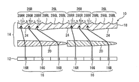
続いて、図3A及び図3Bを参照しながら、光路変更装置14の動作について説明する。第2レンズ部材20が図3Aに示す状態では、各サブ画素16R,16G,16Bの発する光の経路は、以下のようになる。
続いて、図3A及び図3Bを参照しながら、光路変更装置14の動作について説明する。第2レンズ部材20が図3Aに示す状態では、各サブ画素16R,16G,16Bの発する光の経路は、以下のようになる。
サブ画素16Rが発する光は、第2レンズ部材20に入射すると、表示パネル12を正面から見たときに当該第2レンズ部材20に重なる2つの内側レンズ面24のうち左側の内側レンズ面24に向かって出射する。サブ画素16Rが発する光は、当該内側レンズ面24に入射した後、表示パネル12を正面から見たときに当該内側レンズ面24に重なる第1外側レンズ面28RRから出射する。
サブ画素16Gが発する光は、第2レンズ部材20に入射すると、上記左側の内側レンズ面24に向かって出射する。サブ画素16Gが発する光は、当該内側レンズ面24に入射した後、表示パネル12を正面から見たときに当該内側レンズ面24に重なる第1外側レンズ面28GRから出射する。
サブ画素16Bが発する光は、第2レンズ部材20に入射すると、上記左側の内側レンズ面24に向かって出射する。サブ画素16Bが発する光は、当該内側レンズ面24に入射した後、表示パネル12を正面から見たときに当該内側レンズ面24に重なる第1外側レンズ面28BRから出射する。
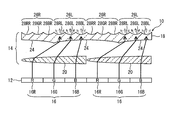
モータ34の回転力が軸30Aに伝達されると、第2レンズ部材20が軸30Aの中心軸線周りに回転する。これにより、第2レンズ部材20は、図3Bに示す状態になる。図3Bに示す状態は、図3Aに示す状態と比べて、第2レンズ部材20が半回転している。図3Bに示す状態では、各サブ画素16R,16G,16Bの発する光の経路は、以下のようになる。
サブ画素16Rが発する光は、第2レンズ部材20に入射すると、表示パネル12を正面から見たときに当該第2レンズ部材20に重なる2つの内側レンズ面24のうち右側の内側レンズ面24に向かって出射する。サブ画素16Rが発する光は、当該内側レンズ面24に入射した後、表示パネル12を正面から見たときに当該内側レンズ面24に重なる第1外側レンズ面28RLから出射する。
サブ画素16Gが発する光は、第2レンズ部材20に入射すると、上記右側の内側レンズ面24に向かって出射する。サブ画素16Gが発する光は、当該内側レンズ面24に入射した後、表示パネル12を正面から見たときに当該内側レンズ面24に重なる第1外側レンズ面28GLから出射する。
サブ画素16Bが発する光は、第2レンズ部材20に入射すると、上記右側の内側レンズ面24に向かって出射する。サブ画素16Bが発する光は、右側の内側レンズ面24に入射した後、表示パネル12を正面から見たときに当該内側レンズ面24に重なる第1外側レンズ面28BLから出射する。
上述のようにして、第2レンズ部材20が回転すると、各サブ画素16R,16G,16Bの発する光は、外側レンズ面26R及び外側レンズ面26Lから交互に出射される。そのため、表示パネル12が表示する画像を、外側レンズ面26Rから出射される画像と、外側レンズ面26Lから出射される画像とに交互に切り替えることにより、見かけ上の画素数が左右方向で2倍になった画像を観察者に見せることができる。
なお、第2レンズ部材20が半回転するタイミングと、表示パネル12が表示する画像を切り換えるタイミングとは、同期させる必要がある。また、複数の第2レンズ部材が半回転するタイミングも同期させる必要がある。
また、表示装置10では、画素16が発する光を色ごとに分割していないので、カラーブレーキングの発生を回避できる。
[第2レンズ部材の駆動方法の応用例]
例えば、図4に示すように、第2レンズ部材20が有する2つのレンズ面21A、21Bの一方をプラスに帯電させ、他方をマイナスに帯電させる。第2レンズ部材20を挟んで一対の電極(図示せず)を配置する。各電極に帯電させる電荷の種類を変化させて、各電極と第2レンズ部材20との間に斥力を発生させる。この斥力により、第2レンズ部材20を回転させる。このようにして、第2レンズ部材20を駆動してもよい。
例えば、図4に示すように、第2レンズ部材20が有する2つのレンズ面21A、21Bの一方をプラスに帯電させ、他方をマイナスに帯電させる。第2レンズ部材20を挟んで一対の電極(図示せず)を配置する。各電極に帯電させる電荷の種類を変化させて、各電極と第2レンズ部材20との間に斥力を発生させる。この斥力により、第2レンズ部材20を回転させる。このようにして、第2レンズ部材20を駆動してもよい。
[第2の実施形態]
続いて、図5及び図6を参照しながら、本発明の第2の実施形態による表示装置10Aについて説明する。表示装置10Aでは、光路変更装置14の代わりに、光路変更装置14Aが採用されている。光路変更装置14Aは、光路変更装置14と比べて、第2レンズ部材及び出射方向制御装置が異なる。
続いて、図5及び図6を参照しながら、本発明の第2の実施形態による表示装置10Aについて説明する。表示装置10Aでは、光路変更装置14の代わりに、光路変更装置14Aが採用されている。光路変更装置14Aは、光路変更装置14と比べて、第2レンズ部材及び出射方向制御装置が異なる。
図5に示すように、本実施形態では、第2レンズ部材20の代わりに、第2レンズ部材20Aが配置される。第2レンズ部材20Aは、所定の断面で延びる板状部材である。第2レンズ部材20Aの断面は、左右方向に延びる基準線L2に対して対称であるとともに、上下方向に延びる基準線L3に対して対称である。第2レンズ部材20Aが有する2つのレンズ面(光が入射する入射面及び光が出射する出射面)は、それぞれ、凸レンズ面である。そのため、第2レンズ部材20Aに入射した光は、特定の方向(第2レンズ部材20Aの左右方向の中央側)に集光される。第2レンズ部材20Aの左右方向の長さは、内側レンズ面24の左右方向の長さの2倍である。つまり、第2レンズ部材20Aの左右方向の長さは、画素16の左右方向の長さの2倍である。
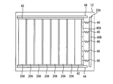
図6に示すように、本実施形態では、出射方向制御装置22の代わりに、出射方向制御装置22Aが配置される。出射方向制御装置22Aは、一対の帯電部材40A,40Bと、ばね46とを含む。帯電部材40Aは、一対の支持部材42,42に取り付けられる。一対の支持部材42,42は、それぞれ、表示パネル12の水平方向(図6の左右方向)に延びて、表示パネル12の水平方向に並ぶ複数の第2レンズ部材20Aを連結する。具体的には、一方の支持部材42は、複数の第2レンズ部材20Aにおける表示パネル12の垂直方向(図6の上下方向)での一端同士(複数の第2レンズ部材20Aにおける長手方向の一端同士)を連結し、他方の支持部材42は、複数の第2レンズ部材20Aにおける表示パネル12の垂直方向での他端同士(複数の第2レンズ部材20Aにおける長手方向の他端同士)を連結する。各支持部材42は、ガイド部材44により、左右方向に移動可能に配置される。ばね46は、一対の帯電部材40A,40Bを連結する。帯電部材40Aは、プラスに帯電している。帯電部材40Bは、マイナスに帯電した状態と、プラス及びマイナスの何れにも帯電していない状態とを取り得る。帯電部材40Bの帯電状態と非帯電状態とは、例えば、図示しないドライブ回路によって実現される。具体的には、例えば、帯電部材40Bに負の電圧を印加することにより、帯電部材40Bをマイナスに帯電させ、帯電部材40Bを接地することにより、帯電部材40Bをプラス及びマイナスの何れにも帯電していない状態にする。
出射方向制御装置22Aにおいては、帯電部材40Bがマイナスに帯電すると、一対の帯電部材40A,40Bの間に発生する引力により、帯電部材40Aが帯電部材40Bに接近する方向に移動する。一方、帯電部材40Bがプラス及びマイナスの何れにも帯電していない場合には、帯電部材40Aは、ばね42の付勢力により、帯電部材40Bから離れる方向に移動する。これにより、各第2レンズ部材22Aは、左右方向に往復変位する。
[光路変更装置の動作]
続いて、図7A及び図7Bを参照しながら、光路変更装置14Aの動作について説明する。第2レンズ部材20Aが図3Aに示す状態、つまり、第2レンズ部材20Aの左右方向の幅中心C4Aが左右方向で隣り合う2つの画素16の境界B3上に位置する状態では、各サブ画素16R,16G,16Bの発する光の経路は、以下のようになる。
続いて、図7A及び図7Bを参照しながら、光路変更装置14Aの動作について説明する。第2レンズ部材20Aが図3Aに示す状態、つまり、第2レンズ部材20Aの左右方向の幅中心C4Aが左右方向で隣り合う2つの画素16の境界B3上に位置する状態では、各サブ画素16R,16G,16Bの発する光の経路は、以下のようになる。
左右方向で隣り合う2つの画素16のうち右側の画素16が有するサブ画素16Rの発する光は、第2レンズ部材20Aに入射すると、表示パネル12を正面から見たときに上記境界B3上に位置する内側レンズ面24に向かって出射する。サブ画素16Rが発する光は、当該内側レンズ面24に入射した後、表示パネル12を正面から見たときに当該内側レンズ面24に重なる第1外側レンズ面28RRから出射する。
上記右側の画素16が有するサブ画素16Gの発する光は、第2レンズ部材20Aに入射すると、表示パネル12を正面から見たときに上記境界B3上に位置する内側レンズ面24に向かって出射する。サブ画素16Gが発する光は、当該内側レンズ面24に入射した後、表示パネル12を正面から見たときに当該内側レンズ面24に重なる第1外側レンズ面28GRから出射する。
上記右側の画素16が有するサブ画素16Bの発する光は、第2レンズ部材20Aに入射すると、表示パネル12を正面から見たときに上記境界B3上に位置する内側レンズ面24に向かって出射する。サブ画素16Bが発する光は、当該内側レンズ面24に入射した後、表示パネル12を正面から見たときに当該内側レンズ面24に重なる第1外側レンズ面28BRから出射する。
左右方向で隣り合う2つの画素16のうち左側の画素16が有するサブ画素16Rの発する光は、第2レンズ部材20Aに入射すると、表示パネル12を正面から見たときに上記境界B3上に位置する内側レンズ面24に向かって出射する。サブ画素16Rが発する光は、当該内側レンズ面24に入射した後、表示パネル12を正面から見たときに当該内側レンズ面24に重なる第1外側レンズ面28RLから出射する。
上記左側の画素16が有するサブ画素16Gの発する光は、第2レンズ部材20Aに入射すると、表示パネル12を正面から見たときに上記境界B3上に位置する内側レンズ面24に向かって出射する。サブ画素16Gが発する光は、当該内側レンズ面24に入射した後、表示パネル12を正面から見たときに当該内側レンズ面24に重なる第1外側レンズ面28GLから出射する。
上記左側の画素16が有するサブ画素16Bの発する光は、第2レンズ部材20Aに入射すると、表示パネル12を正面から見たときに上記境界B3上に位置する内側レンズ面24に向かって出射する。サブ画素16Bが発する光は、当該内側レンズ面24に入射した後、表示パネル12を正面から見たときに当該内側レンズ面24に重なる第1外側レンズ面28BLから出射する。
一対の帯電部材40A、40Bの間に発生する引力により、第2レンズ部材20Aが左右方向に移動する。これにより、第2レンズ部材20Aは、図7Bに示す状態になる。図7Bに示す状態は、図7Aに示す状態と比べて、第2レンズ部材20Aが水平方向に1画素分移動している。これにより、図7Bに示す状態では、図7Aに示す状態と比べて、上記境界B3を挟んで2つの第2レンズ部材20Aが位置する。図7Bに示す状態では、各サブ画素16R,16G,16Bの発する光の経路は、以下のようになる。
左右方向で隣り合う2つの画素16のうち右側の画素16が有するサブ画素16Rの発する光は、境界B3よりも右側に位置する第2レンズ部材20Aに入射すると、表示パネル12を正面から見たときに上記境界B3上に位置する内側レンズ面24の右隣に位置する内側レンズ面24に向かって出射する。サブ画素16Rが発する光は、当該内側レンズ面24に入射した後、表示パネル12を正面から見たときに当該内側レンズ面24に重なる第1外側レンズ面28RLから出射する。
上記右側の画素16が有するサブ画素16Gの発する光は、境界B3よりも右側に位置する第2レンズ部材20Aに入射すると、表示パネル12を正面から見たときに上記境界B3上に位置する内側レンズ面24の右隣に位置する内側レンズ面24に向かって出射する。サブ画素16Gが発する光は、当該内側レンズ面24に入射した後、表示パネル12を正面から見たときに当該内側レンズ面24に重なる第1外側レンズ面28GLから出射する。
上記右側の画素16が有するサブ画素16Bの発する光は、境界B3よりも右側に位置する第2レンズ部材20Aに入射すると、表示パネル12を正面から見たときに上記境界B3上に位置する内側レンズ面24の右隣に位置する内側レンズ面24に向かって出射する。サブ画素16Bが発する光は、当該内側レンズ面24に入射した後、表示パネル12を正面から見たときに当該内側レンズ面24に重なる第1外側レンズ面28BLから出射する。
左右方向で隣り合う2つの画素16のうち左側の画素16が有するサブ画素16Rの発する光は、境界B3よりも左側に位置する第2レンズ部材20Aに入射すると、表示パネル12を正面から見たときに上記境界B3上に位置する内側レンズ面24の左隣に位置する内側レンズ面24に向かって出射する。サブ画素16Rが発する光は、当該内側レンズ面24に入射した後、表示パネル12を正面から見たときに当該内側レンズ面24に重なる第1外側レンズ面28RRから出射する。
上記左側の画素16が有するサブ画素16Gの発する光は、境界B3よりも左側に位置する第2レンズ部材20Aに入射すると、表示パネル12を正面から見たときに上記境界B3上に位置する内側レンズ面24の左隣に位置する内側レンズ面24に向かって出射する。サブ画素16Gが発する光は、当該内側レンズ面24に入射した後、表示パネル12を正面から見たときに当該内側レンズ面24に重なる第1外側レンズ面28GRから出射する。
上記左側の画素16が有するサブ画素16Bの発する光は、境界B3よりも左側に位置する第2レンズ部材20Aに入射すると、表示パネル12を正面から見たときに上記境界B3上に位置する内側レンズ面24の左隣に位置する内側レンズ面24に向かって出射する。サブ画素16Bが発する光は、当該内側レンズ面24に入射した後、表示パネル12を正面から見たときに当該内側レンズ面24に重なる第1外側レンズ面28BRから出射する。
上述のようにして、第2レンズ部材20Aが移動すると、各サブ画素16R,16G,16Bの発する光は、外側レンズ面26R及び外側レンズ面26Lから交互に出射される。そのため、表示パネル12が表示する画像を、外側レンズ面26Rから出射される画像と、外側レンズ面26Lから出射される画像とに交互に切り替えることにより、見かけ上の画素数が左右方向で2倍になった画像を観察者に見せることができる。
なお、第2レンズ部材20Aが1画素分移動するタイミングと、表示パネル12が表示する画像を切り換えるタイミングとは、同期させる必要がある。
[第3の実施形態]
続いて、図8及び図9を参照しながら、本発明の第3の実施形態による表示装置10Bについて説明する。表示装置10Bでは、光路変更装置14の代わりに、光路変更装置14Bが採用されている。光路変更装置14Bは、光路変更装置14と比べて、第2レンズ部材及び出射方向制御装置が異なる。
続いて、図8及び図9を参照しながら、本発明の第3の実施形態による表示装置10Bについて説明する。表示装置10Bでは、光路変更装置14の代わりに、光路変更装置14Bが採用されている。光路変更装置14Bは、光路変更装置14と比べて、第2レンズ部材及び出射方向制御装置が異なる。
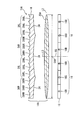
図8に示すように、本実施形態では、第2レンズ部材20の代わりに、第2レンズ部材20Bが設けられる。第2レンズ部材20Bは、図8及び図9に示すように、基板50と、複数の溝52と、撥水性誘電膜54と、電極56と、油膜58と、液体60とを備える。基板50は、第1レンズ部材18に対向して配置される。複数の溝52は、基板50の第1レンズ部材18と対向する面において、左右方向に並んで形成される。撥水性誘電膜54は、各溝52の内面に配置される。電極56は、各溝52が有する一対の壁52A,52Aのそれぞれに配置され、撥水性誘電膜54で覆われる。油膜58は、撥水性誘電膜54に接して配置され、各溝52に収容される。液体60は、油膜58と分離して配置され、油膜58を覆う。本実施形態では、液体60は、撥水性誘電膜54と第1レンズ部材18との間に封入される。液体60は、例えば、水である。
図9に示すように、本実施形態では、出射方向制御装置22の代わりに、出射方向制御装置22Bが設けられている。出射方向制御装置22Bは、電極56と、駆動回路62とを含む。駆動回路62は、電極56に電圧を印加するとともに、電極56に印加する電圧を変化させる。右側の電極56に印加する電圧と左側の電極56に印加する電圧とを異ならせることにより、油膜54と液体60との界面が変化する。つまり、本実施形態では、エレクトロウェッティングにより、油膜54と液体60との界面を制御する。油膜54と液体60との界面を制御することにより、表示パネル12を正面から見たときに1つの画素16に重なる幾つかの油膜58と液体60との界面を、第1の実施形態と同様なレンズ面、つまり、第2レンズ部材20における第1レンズ部材18側のレンズ面(出射面)にすることができる。その結果、画素16の発する光が油膜58から出射するときの方向を変化させることができる。したがって、第1の実施形態と同様に、左右方向の見かけ上の画素数を2倍にすることができる。
以上、本発明の実施形態について、詳述してきたが、これらはあくまでも例示であって、本発明は、上述の実施形態によって、何等、限定されない。
例えば、第1及び第2の実施形態において、画素は、黄色の光を発するサブ画素をさらに含んでもよいし、モノクロの画素であってもよい。
Claims (5)
- 所定の方向に並んで複数形成される画素を有する表示パネルと、
前記表示パネルよりも観察者側に配置され、前記画素が発する光の経路を変更する光路変更装置とを備え、
前記光路変更装置は、
第1レンズ部材と、
前記第1レンズ部材よりも前記表示パネル側において、前記所定方向に並んで複数配置される第2レンズ部材と、
前記第2レンズ部材に入射した前記画素の光が前記第2レンズ部材から出射する方向を変化させる出射方向制御装置とを備え、
前記第1レンズ部材は、
前記表示パネル側において前記所定の方向に並んで複数形成される内側レンズ面と、
観察者側において前記所定の方向に並んで形成され、前記表示パネルを正面から見たときに前記内側レンズ面に重なる一対の外側レンズ面とを備え、
前記第2レンズ部材に入射した前記画素の光が前記第2レンズ部材から出射する方向に応じて、前記内側レンズ面に入射した前記画素の光が前記一対の外側レンズ面の何れかから出射する、表示装置。 - 請求項1に記載の表示装置であって、
前記第2レンズ部材は、第1の位置と、前記第1の位置とは異なる第2の位置との間で回転可能に配置され、
前記第2レンズが前記第1の位置にあるときと、前記第2レンズが前記第2の位置にあるときとで、前記画素の光が異なる方向に集光される、表示装置。 - 請求項1に記載の表示装置であって、
前記第2レンズ部材は、第1の位置と、前記第1の位置とは異なる第2の位置との間で往復移動可能に配置され、
前記第2レンズが前記第1の位置にあるときと、前記第2レンズが前記第2の位置にあるときとで、前記画素の光が異なる方向に集光される、表示装置。 - 請求項1に記載の表示装置であって、
前記第2レンズ部材は、
前記第1レンズ部材に対向して配置される基板と、
前記基板の前記第1レンズ部材と対向する面において、前記所定の方向に並んで複数形成される溝と、
前記溝の内面に配置される撥水性誘電膜と、
前記溝が有する一対の壁のそれぞれに配置され、前記撥水性誘電膜で覆われる電極と、
前記撥水性誘電膜に接して配置され、前記溝に収容される油膜と、
前記油膜と分離して配置され、前記油膜を覆う液体とを備え、
前記出射方向制御装置は、前記電極に印加する電圧を変化させる、表示装置。 - 請求項1~4の何れか1項に記載の表示装置であって、
前記画素は、互いに異なる色の光を発するとともに、前記所定の方向に並んで複数形成されるサブ画素を含み、
前記一対の外側レンズ面は、それぞれ、各サブ画素に対応する第1外側レンズ面を含む、表示装置。
Priority Applications (1)
| Application Number | Priority Date | Filing Date | Title |
|---|---|---|---|
| US14/758,713 US20150370064A1 (en) | 2013-01-08 | 2013-12-24 | Display device |
Applications Claiming Priority (2)
| Application Number | Priority Date | Filing Date | Title |
|---|---|---|---|
| JP2013-001262 | 2013-01-08 | ||
| JP2013001262 | 2013-01-08 |
Publications (1)
| Publication Number | Publication Date |
|---|---|
| WO2014109225A1 true WO2014109225A1 (ja) | 2014-07-17 |
Family
ID=51166882
Family Applications (1)
| Application Number | Title | Priority Date | Filing Date |
|---|---|---|---|
| PCT/JP2013/084517 Ceased WO2014109225A1 (ja) | 2013-01-08 | 2013-12-24 | 表示装置 |
Country Status (2)
| Country | Link |
|---|---|
| US (1) | US20150370064A1 (ja) |
| WO (1) | WO2014109225A1 (ja) |
Families Citing this family (2)
| Publication number | Priority date | Publication date | Assignee | Title |
|---|---|---|---|---|
| FR3096510B1 (fr) * | 2019-05-24 | 2021-05-28 | Aledia | Dispositif optoélectronique ayant des systèmes optiques déplaçables entre différents pixels et procédé de contrôle |
| KR102953421B1 (ko) * | 2020-09-11 | 2026-04-15 | 엘지디스플레이 주식회사 | 광경로제어부재를 구비한 표시장치 |
Citations (7)
| Publication number | Priority date | Publication date | Assignee | Title |
|---|---|---|---|---|
| JPH06110050A (ja) * | 1992-09-25 | 1994-04-22 | Hitachi Ltd | 液晶表示装置 |
| JPH11101949A (ja) * | 1997-09-29 | 1999-04-13 | Matsushita Electric Ind Co Ltd | 照明手段と当該手段を用いた照明装置及び投写型表示装置 |
| JP2005084431A (ja) * | 2003-09-09 | 2005-03-31 | Sharp Corp | 表示装置 |
| JP2005326574A (ja) * | 2004-05-13 | 2005-11-24 | Ricoh Co Ltd | 空間光変調装置及び画像表示装置 |
| JP2006184645A (ja) * | 2004-12-28 | 2006-07-13 | Konica Minolta Photo Imaging Inc | 立体画像形成システム |
| JP2009015150A (ja) * | 2007-07-06 | 2009-01-22 | Ntt Docomo Inc | 複数視点提示ディスプレイ装置及び表示制御方法 |
| JP2012078696A (ja) * | 2010-10-05 | 2012-04-19 | Jvc Kenwood Corp | 裸眼立体ディスプレイ装置 |
Family Cites Families (3)
| Publication number | Priority date | Publication date | Assignee | Title |
|---|---|---|---|---|
| US5642226A (en) * | 1995-01-18 | 1997-06-24 | Rosenthal; Bruce A. | Lenticular optical system |
| GB2403815A (en) * | 2003-07-10 | 2005-01-12 | Ocuity Ltd | Birefringent lens array structure |
| US8310757B2 (en) * | 2008-08-28 | 2012-11-13 | Smartershade, Inc. | Wire grid polarizers in window shading applications and varying thickness wave retarders |
-
2013
- 2013-12-24 US US14/758,713 patent/US20150370064A1/en not_active Abandoned
- 2013-12-24 WO PCT/JP2013/084517 patent/WO2014109225A1/ja not_active Ceased
Patent Citations (7)
| Publication number | Priority date | Publication date | Assignee | Title |
|---|---|---|---|---|
| JPH06110050A (ja) * | 1992-09-25 | 1994-04-22 | Hitachi Ltd | 液晶表示装置 |
| JPH11101949A (ja) * | 1997-09-29 | 1999-04-13 | Matsushita Electric Ind Co Ltd | 照明手段と当該手段を用いた照明装置及び投写型表示装置 |
| JP2005084431A (ja) * | 2003-09-09 | 2005-03-31 | Sharp Corp | 表示装置 |
| JP2005326574A (ja) * | 2004-05-13 | 2005-11-24 | Ricoh Co Ltd | 空間光変調装置及び画像表示装置 |
| JP2006184645A (ja) * | 2004-12-28 | 2006-07-13 | Konica Minolta Photo Imaging Inc | 立体画像形成システム |
| JP2009015150A (ja) * | 2007-07-06 | 2009-01-22 | Ntt Docomo Inc | 複数視点提示ディスプレイ装置及び表示制御方法 |
| JP2012078696A (ja) * | 2010-10-05 | 2012-04-19 | Jvc Kenwood Corp | 裸眼立体ディスプレイ装置 |
Also Published As
| Publication number | Publication date |
|---|---|
| US20150370064A1 (en) | 2015-12-24 |
Similar Documents
| Publication | Publication Date | Title |
|---|---|---|
| JP5152718B2 (ja) | 画像表示装置および端末装置 | |
| KR102795189B1 (ko) | 헤드 마운티드 디스플레이 장치 | |
| KR101866874B1 (ko) | 전기습윤 프리즘 소자 및 이를 이용하는 다시점 3차원 영상 디스플레이 장치 | |
| US20070096125A1 (en) | Illumination device | |
| JP2011043623A (ja) | 立体映像表示装置 | |
| US20100271352A1 (en) | Display device and method for manufacturing the same | |
| CN105190409B (zh) | 立体显示装置 | |
| KR100617926B1 (ko) | 표시 장치 | |
| WO2012169466A1 (ja) | 表示装置 | |
| KR20130024102A (ko) | 전기 습윤 소자 및 그 제조 방법 | |
| JP5449238B2 (ja) | 三次元映像表示装置 | |
| WO2011111263A1 (ja) | 表示素子、及びこれを用いた電気機器 | |
| US20130163068A1 (en) | Display element and electrical apparatus using same | |
| WO2014109225A1 (ja) | 表示装置 | |
| JP2015535349A (ja) | エレクトロウェッティング表示デバイス | |
| KR20120023510A (ko) | 디스플레이 장치 | |
| WO2012066970A1 (ja) | 表示素子、及びこれを用いた電気機器 | |
| JP2009008912A (ja) | 画像表示装置及びそのための画像表示用遮光基板 | |
| WO2012002013A1 (ja) | 表示素子、及びこれを用いた電気機器 | |
| WO2012141078A1 (ja) | 立体表示装置 | |
| US20170269357A1 (en) | Stereoscopic display device | |
| WO2012098987A1 (ja) | 表示素子、及びこれを用いた電気機器 | |
| JP4862415B2 (ja) | 空間光変調装置及びこれを用いた表示装置 | |
| JP2014137511A (ja) | 立体画像表示装置 | |
| JP5472840B2 (ja) | 画像表示装置および端末装置 |
Legal Events
| Date | Code | Title | Description |
|---|---|---|---|
| 121 | Ep: the epo has been informed by wipo that ep was designated in this application |
Ref document number: 13870801 Country of ref document: EP Kind code of ref document: A1 |
|
| WWE | Wipo information: entry into national phase |
Ref document number: 14758713 Country of ref document: US |
|
| NENP | Non-entry into the national phase |
Ref country code: DE |
|
| 122 | Ep: pct application non-entry in european phase |
Ref document number: 13870801 Country of ref document: EP Kind code of ref document: A1 |
|
| NENP | Non-entry into the national phase |
Ref country code: JP |