WO2014108940A1 - 電界効果トランジスタ - Google Patents
電界効果トランジスタ Download PDFInfo
- Publication number
- WO2014108940A1 WO2014108940A1 PCT/JP2013/001344 JP2013001344W WO2014108940A1 WO 2014108940 A1 WO2014108940 A1 WO 2014108940A1 JP 2013001344 W JP2013001344 W JP 2013001344W WO 2014108940 A1 WO2014108940 A1 WO 2014108940A1
- Authority
- WO
- WIPO (PCT)
- Prior art keywords
- region
- superlattice
- channel
- impurity
- drain
- Prior art date
- Legal status (The legal status is an assumption and is not a legal conclusion. Google has not performed a legal analysis and makes no representation as to the accuracy of the status listed.)
- Ceased
Links
Images
Classifications
-
- H—ELECTRICITY
- H10—SEMICONDUCTOR DEVICES; ELECTRIC SOLID-STATE DEVICES NOT OTHERWISE PROVIDED FOR
- H10D—INORGANIC ELECTRIC SEMICONDUCTOR DEVICES
- H10D62/00—Semiconductor bodies, or regions thereof, of devices having potential barriers
- H10D62/80—Semiconductor bodies, or regions thereof, of devices having potential barriers characterised by the materials
- H10D62/81—Semiconductor bodies, or regions thereof, of devices having potential barriers characterised by the materials of structures exhibiting quantum-confinement effects, e.g. single quantum wells; of structures having periodic or quasi-periodic potential variation
- H10D62/815—Semiconductor bodies, or regions thereof, of devices having potential barriers characterised by the materials of structures exhibiting quantum-confinement effects, e.g. single quantum wells; of structures having periodic or quasi-periodic potential variation of structures having periodic or quasi-periodic potential variation, e.g. superlattices or multiple quantum wells [MQW]
- H10D62/8161—Semiconductor bodies, or regions thereof, of devices having potential barriers characterised by the materials of structures exhibiting quantum-confinement effects, e.g. single quantum wells; of structures having periodic or quasi-periodic potential variation of structures having periodic or quasi-periodic potential variation, e.g. superlattices or multiple quantum wells [MQW] potential variation due to variations in composition or crystallinity, e.g. heterojunction superlattices
- H10D62/8162—Semiconductor bodies, or regions thereof, of devices having potential barriers characterised by the materials of structures exhibiting quantum-confinement effects, e.g. single quantum wells; of structures having periodic or quasi-periodic potential variation of structures having periodic or quasi-periodic potential variation, e.g. superlattices or multiple quantum wells [MQW] potential variation due to variations in composition or crystallinity, e.g. heterojunction superlattices having quantum effects only in the vertical direction, i.e. layered structures having quantum effects solely resulting from vertical potential variation
- H10D62/8164—Semiconductor bodies, or regions thereof, of devices having potential barriers characterised by the materials of structures exhibiting quantum-confinement effects, e.g. single quantum wells; of structures having periodic or quasi-periodic potential variation of structures having periodic or quasi-periodic potential variation, e.g. superlattices or multiple quantum wells [MQW] potential variation due to variations in composition or crystallinity, e.g. heterojunction superlattices having quantum effects only in the vertical direction, i.e. layered structures having quantum effects solely resulting from vertical potential variation comprising only semiconductor materials
-
- H—ELECTRICITY
- H10—SEMICONDUCTOR DEVICES; ELECTRIC SOLID-STATE DEVICES NOT OTHERWISE PROVIDED FOR
- H10D—INORGANIC ELECTRIC SEMICONDUCTOR DEVICES
- H10D30/00—Field-effect transistors [FET]
- H10D30/01—Manufacture or treatment
- H10D30/015—Manufacture or treatment of FETs having heterojunction interface channels or heterojunction gate electrodes, e.g. HEMT
-
- H—ELECTRICITY
- H10—SEMICONDUCTOR DEVICES; ELECTRIC SOLID-STATE DEVICES NOT OTHERWISE PROVIDED FOR
- H10D—INORGANIC ELECTRIC SEMICONDUCTOR DEVICES
- H10D48/00—Individual devices not covered by groups H10D1/00 - H10D44/00
- H10D48/383—Quantum effect devices, e.g. of devices using quantum reflection, diffraction or interference effects
-
- H—ELECTRICITY
- H10—SEMICONDUCTOR DEVICES; ELECTRIC SOLID-STATE DEVICES NOT OTHERWISE PROVIDED FOR
- H10D—INORGANIC ELECTRIC SEMICONDUCTOR DEVICES
- H10D62/00—Semiconductor bodies, or regions thereof, of devices having potential barriers
- H10D62/10—Shapes, relative sizes or dispositions of the regions of the semiconductor bodies; Shapes of the semiconductor bodies
- H10D62/13—Semiconductor regions connected to electrodes carrying current to be rectified, amplified or switched, e.g. source or drain regions
- H10D62/165—Tunnel injectors
-
- H—ELECTRICITY
- H10—SEMICONDUCTOR DEVICES; ELECTRIC SOLID-STATE DEVICES NOT OTHERWISE PROVIDED FOR
- H10D—INORGANIC ELECTRIC SEMICONDUCTOR DEVICES
- H10D62/00—Semiconductor bodies, or regions thereof, of devices having potential barriers
- H10D62/10—Shapes, relative sizes or dispositions of the regions of the semiconductor bodies; Shapes of the semiconductor bodies
- H10D62/17—Semiconductor regions connected to electrodes not carrying current to be rectified, amplified or switched, e.g. channel regions
- H10D62/351—Substrate regions of field-effect devices
- H10D62/357—Substrate regions of field-effect devices of FETs
- H10D62/364—Substrate regions of field-effect devices of FETs of IGFETs
-
- H—ELECTRICITY
- H10—SEMICONDUCTOR DEVICES; ELECTRIC SOLID-STATE DEVICES NOT OTHERWISE PROVIDED FOR
- H10D—INORGANIC ELECTRIC SEMICONDUCTOR DEVICES
- H10D62/00—Semiconductor bodies, or regions thereof, of devices having potential barriers
- H10D62/80—Semiconductor bodies, or regions thereof, of devices having potential barriers characterised by the materials
- H10D62/81—Semiconductor bodies, or regions thereof, of devices having potential barriers characterised by the materials of structures exhibiting quantum-confinement effects, e.g. single quantum wells; of structures having periodic or quasi-periodic potential variation
- H10D62/815—Semiconductor bodies, or regions thereof, of devices having potential barriers characterised by the materials of structures exhibiting quantum-confinement effects, e.g. single quantum wells; of structures having periodic or quasi-periodic potential variation of structures having periodic or quasi-periodic potential variation, e.g. superlattices or multiple quantum wells [MQW]
-
- H—ELECTRICITY
- H10—SEMICONDUCTOR DEVICES; ELECTRIC SOLID-STATE DEVICES NOT OTHERWISE PROVIDED FOR
- H10D—INORGANIC ELECTRIC SEMICONDUCTOR DEVICES
- H10D64/00—Electrodes of devices having potential barriers
- H10D64/20—Electrodes characterised by their shapes, relative sizes or dispositions
- H10D64/23—Electrodes carrying the current to be rectified, amplified, oscillated or switched, e.g. sources, drains, anodes or cathodes
- H10D64/251—Source or drain electrodes for field-effect devices
- H10D64/252—Source or drain electrodes for field-effect devices for vertical or pseudo-vertical devices
-
- H—ELECTRICITY
- H10—SEMICONDUCTOR DEVICES; ELECTRIC SOLID-STATE DEVICES NOT OTHERWISE PROVIDED FOR
- H10D—INORGANIC ELECTRIC SEMICONDUCTOR DEVICES
- H10D62/00—Semiconductor bodies, or regions thereof, of devices having potential barriers
- H10D62/10—Shapes, relative sizes or dispositions of the regions of the semiconductor bodies; Shapes of the semiconductor bodies
- H10D62/117—Shapes of semiconductor bodies
- H10D62/118—Nanostructure semiconductor bodies
- H10D62/119—Nanowire, nanosheet or nanotube semiconductor bodies
- H10D62/122—Nanowire, nanosheet or nanotube semiconductor bodies oriented at angles to substrates, e.g. perpendicular to substrates
-
- H—ELECTRICITY
- H10—SEMICONDUCTOR DEVICES; ELECTRIC SOLID-STATE DEVICES NOT OTHERWISE PROVIDED FOR
- H10D—INORGANIC ELECTRIC SEMICONDUCTOR DEVICES
- H10D62/00—Semiconductor bodies, or regions thereof, of devices having potential barriers
- H10D62/80—Semiconductor bodies, or regions thereof, of devices having potential barriers characterised by the materials
- H10D62/85—Semiconductor bodies, or regions thereof, of devices having potential barriers characterised by the materials being Group III-V materials, e.g. GaAs
- H10D62/8503—Nitride Group III-V materials, e.g. AlN or GaN
Definitions
- the present invention relates to a semiconductor field effect transistor (FET).
- FET semiconductor field effect transistor
- SS subthreshold slope
- the conventionally proposed tunnel FET has a large resistance at the time of tunneling, and a high on-current cannot be made compatible with the steep SS characteristics. Therefore, the source of the field effect transistor is doped and has a large number of carriers.
- a transistor including a lattice has been proposed (Patent Document 1). In this transistor, high carrier current is satisfied by supplying carriers filled in the tolerance band of the miniband, and when the forbidden band of the miniband overlaps with the channel, the supply of the carrier is stopped. Since the energy difference between the band and the tolerance band can be changed by the design of the superlattice, a sharp on / off switching can be designed.
- the present inventor has recognized the following problems.
- a superlattice doped with a high concentration specifically, 10 19 / cm 3 or more.
- concentration order of 10 19 / cm 3 means that the dopant is mixed at a ratio of several tens per cubic volume of a 10 nm side.
- the thickness of the superlattice layer is at most about 3 to 4 nm, doping in the order of a concentration of 10 19 / cm 3 causes a dopant to exist in a certain layer, and no dopant exists in a certain layer.
- the dopant is randomly mixed in the superlattice.
- Randomly existing dopants disturb the potential formed by the superlattice and cause the problem of breaking the miniband.
- the present invention has been made in view of such a problem, and one of exemplary purposes of an aspect thereof is to provide an FET capable of realizing a high concentration carrier while maintaining a good miniband.
- An embodiment of the present invention relates to a field effect transistor including a channel region and a superlattice region between source and drain electrodes.
- a field effect transistor including a channel region and a superlattice region between source and drain electrodes.
- an impurity doping region in which impurities are diffused is formed around the superlattice region.
- a high-concentration carrier is formed from the impurity-doped region in the peripheral region, thereby forming a high-concentration carrier from the impurity-doped region. Can be supplied to the channel region. Thereby, a high concentration carrier can be realized while maintaining a good miniband.
- a high concentration carrier can be realized while maintaining a good miniband.
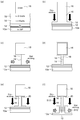
- FIG. 2A to 2F are cross-sectional views showing a method for manufacturing the FET of FIG.
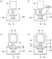
- FIGS. 3A to 3D are cross-sectional views showing a method for manufacturing the FET of FIG.
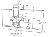
- FIG. 4 is a perspective view illustrating a configuration of an N-channel FET according to the second modification.
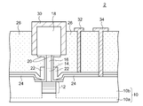
- FIG. 1 is a cross-sectional view showing a configuration of an N-channel FET 2 according to the embodiment.
- the FET 2 is a group III-V compound semiconductor transistor, and includes an impurity doping region 10, a superlattice region 12, a channel region 14, a drain region 16, a drain electrode 18, a gate insulating film 20, a gate electrode 22, an insulating film 24, and an interlayer insulation.
- a film 26, a drain extraction electrode 30, a gate extraction electrode 32, and a source extraction electrode 34 are provided.
- the region surrounding the superlattice region 12, more specifically, the region in contact with the side surface and the bottom surface thereof is doped with n-type impurities at a high concentration, specifically about 2 to 10 ⁇ 10 19 cm ⁇ 3.
- Impurity doping regions 10 that are the formed semiconductor layers are formed.
- the impurity doped region 10 and the superlattice region 12 are source regions that supply carriers to the channel region 14, and in this embodiment, the impurity doped region 10 also serves as a source electrode.
- a region in contact with the bottom surface of the superlattice region 12 is referred to as a first impurity doping region 10 a, and a region in contact with the side surface of the superlattice region 12 is referred to as a second impurity doping region 10 b.
- These may be integrally formed without being distinguished, or may be formed as separate regions.
- the impurity doping region 10 may be formed of indium phosphide (n-InP) doped with n-type impurities, which can efficiently supply carriers to the InGaAs / InP superlattice region 12 using band discontinuity. .
- n-InP indium phosphide
- an n-InGaAs layer may be formed between the impurity doped region 10 and the InP substrate as shown in Modification Example 2 described later.
- the impurity doping region 10 may be formed of n-InGaAs whose band is continuous with the superlattice region 12, or may be formed of indium gallium arsenide phosphorus (n-InGaAsP) having an appropriate band discontinuity. Good. Moreover, when forming the 1st impurity doping area
- the drain region 16 is formed on the channel region 14.
- the drain region 16 is indium gallium arsenide (n-InGaAs) doped with the first conductivity, and can be formed by doping the same InGaAs as the channel region 14 with an n-type impurity.
- the drain electrode 18 is formed on the drain region 16.
- the drain electrode 18 is made of, for example, tungsten silicide (WSi).
- a gate insulating film 20 is formed along the side walls of the channel region 14 and the drain region 16.
- Examples of the material of the gate insulating film 20 include silicon dioxide (SiO 2 ), high-k material aluminum oxide (Al 2 O 3 ), hafnium oxide (HfO 2 ), and the like.
- a gate electrode 22 is formed so as to sandwich the channel region 14 with the gate insulating film 20 interposed therebetween.
- aluminum (Al) is used for the gate electrode 22.
- An insulating film 24 is formed between the gate electrode 22 and the impurity doping region 10b in order to reduce the parasitic capacitance in the vicinity of the leading edge between layers and the superlattice region 12.
- the material of the insulating film 24 include vapor-deposited insulating film materials such as Al 2 O 3 and SiO 2 .
- An interlayer insulating film 26 such as BCB (benzocyclobutene) is formed on the gate electrode 22.
- BCB benzocyclobutene
- the drain extraction electrode 30, the gate extraction electrode 32, and the source extraction electrode 34 are connected to the drain electrode 18, the gate electrode 22, and the impurity doping region 10 through the opening of the interlayer insulating film 26.
- FIGS. 3 (a) to 3 (d) are cross-sectional views showing a method for manufacturing the FET 2 of FIG.
- the manufacturing method demonstrated here is an example, and the manufacturing method of FET2 which concerns on this invention is not limited to it.
- a superlattice region (InGaAs / InP) 12 a channel region (i-InGaAs layer) 14, on the n-InP substrate that becomes the first impurity doping region 10a by crystal growth,
- a drain region (n-InGaAs layer) 16 is formed in order.
- the channel length is determined by the layer thickness of the channel region 14.
- the carrier concentration of the impurity doping region (n-InP) 10 is about 2 to 10 ⁇ 10 19 cm ⁇ 3 .
- a striped drain electrode 18 is formed on the drain region 16.
- the drain electrode is formed to be several tens of nm wider than the final channel width of 5 to 20 nm.
- etching is performed to the depth of the channel region 14 by dry etching, for example, reactive ion etching (RIE) to reach the superlattice region 12. Stop etching before.
- RIE reactive ion etching
- ICP inductively coupled
- both sides of the channel region 14 are etched with a selective wet etchant (for example, a citric acid-based etchant) to narrow the mesa width.
- a selective wet etchant for example, a citric acid-based etchant
- an insulating film 19 such as SiO 2 , Al 2 O 3 , or HfO 2 is uniformly deposited on the entire surface by using an atomic layer deposition method or the like (FIG. 2D).
- the insulating film other than the side wall of the channel region 14 is removed by dry etching, for example, RIE using CF 4 (carbon tetrafluoride) using the drain electrode 18 as a mask. To do. Thereby, the gate insulating film 20 is formed.
- the superlattice region 12 is etched by dry etching, for example, ICP-RIE using methane / hydrogen, using the drain electrode 18 as a mask (S10).
- the sidewalls of the superlattice region 12 are etched by wet etching (for example, bromomethanol) to reduce the size (S12).
- the width of the superlattice region 12 to be left is about 10 to 20 nm larger than the channel width to be finally formed.
- the second impurity doping region (n-InP layer) 10b is grown under a selective growth condition that does not grow on the insulating film 20 on the sidewalls of the drain electrode 18 and the channel region 14. Do growth.
- the upper end of the formed impurity doping region 10 b is higher than the superlattice region 12.
- an insulating film 24 such as Al 2 O 3 or SiO 2 is formed by deposition with an angle.
- the drain extraction electrode 30 and the gate electrode 22 are formed.
- the gate electrode 22 is formed by vapor deposition at an angle so as to be insulated from the drain extraction electrode 30 in a self-aligning manner. If the channel side surface can be damaged by the growth of the second impurity-doped region 10b, the gate insulating film 20 is temporarily removed immediately before the gate electrode 22 is formed, and the channel side surface is thinly etched to remove the damage. It is preferable to form the gate insulating film 20 again. Thereby, good characteristics of the gate insulating film 20 can be obtained.
- the entire device is covered with an interlayer insulating film 26 by spin coating, and only the drain extraction electrode 30 is cueed and exposed. Thereafter, a window is opened in the interlayer insulating film 26, and a gate extraction electrode 32 and a source extraction electrode 34 are formed.
- the impurity doped region 10b which is a semiconductor doped with impurities, the first impurity doped region 10a, and the superlattice region 12 are adjacent to each other, whereby the impurity doped region 10b and the first impurity doped region 10b are formed in the superlattice region 12.
- Carriers can be supplied from one impurity-doped region 10a. This eliminates the need for high-concentration doping in the superlattice region 12, thereby realizing high-concentration carriers while maintaining a good miniband.
- the voltage-current characteristics of the transistor are determined by the carrier amount and distribution in the source region. Therefore, voltage-current characteristics (for example, steep on / off characteristics, high on-current characteristics, etc.) can be designed flexibly and freely.
- the channel region 14 is made of i-InGaAs and the superlattice region 12 is made of InGaAs / InP has been described.
- the superlattice region 12 may have a laminated structure (InGaAs / AlInAs) of indium gallium arsenide and aluminum indium arsenide.
- the channel region 14 is gallium nitride (GaN)
- the superlattice region 12 may have a laminated structure of AlGaN / GaN.
- FIG. 4 is a perspective view illustrating a configuration of an N-channel FET according to the second modification.
- the impurity doping region 10 is formed of n-InP
- an n-InGaAs layer 13 is formed between the impurity doping region 10 and the InP substrate 11.
- An n-InGaAs layer 15 is also formed between the source extraction electrode 34 and the InP substrate 11.
- Modification 3 In the embodiment, an N-channel FET that supplies electrons from a source has been described. However, the present invention can also be applied to a P-channel FET that supplies holes to a channel. In this case, the polarity of the diffusing impurity (dopant) may be changed from n-type to p-type.
- Modification 5 In the embodiment, the structure in which the layers of the superlattice region 12 are stacked in the vertical direction with respect to the substrate and the carrier moves in the vertical direction has been described, but the present invention is not limited thereto.
- the layer of the superlattice region 12 may be stacked parallel to the substrate, that is, in the horizontal direction, and the carrier may move in the horizontal direction.
- the present invention relates to a semiconductor field effect transistor (FET).
- FET semiconductor field effect transistor
Landscapes
- Junction Field-Effect Transistors (AREA)
- Insulated Gate Type Field-Effect Transistor (AREA)
Abstract
ソース・ドレイン電極間にチャネル領域14および超格子領域12を備えるFET2が提供される。チャネル領域14は、超格子領域12の一面に接する領域に形成される。チャネル領域14と隣接して、ドレイン領域16、ドレイン電極18が順に形成される。超格子領域12の周囲には、不純物が拡散された不純物ドーピング領域10が形成される。
Description
本発明は、半導体電界効果トランジスタ(FET:Field Effect Transistor)に関する。
高速低消費電力デバイスの実現には、低電圧で高いオン電流を流すための高移動度を持つ化合物半導体がチャネル材料として研究されているが、低消費電力動作のためにはオフ時の電流を小さくすることも重要である。低電圧でオフ電流を小さくするためには、ゲートソース間しきい値電圧(以下、単にしきい値電圧と称する)以下における電圧の変化に対する電流の変化を示すサブスレッショルドスロープ(SS)特性を小さくする必要があり、従来のキャリアの熱分布限界から一桁変化させるために、室温で60mV/decを下回る急峻なSS特性を得る必要がある。
従来提案されているトンネルFETではトンネル時の抵抗が大きく、高いオン電流を急峻なSS特性と両立させることが出来なかったことから、電界効果トランジスタのソースにドーピングして多くのキャリヤを持った超格子を入れたトランジスタが提案されている(特許文献1)。このトランジスタでは、ミニバンドの許容帯に満たされたキャリヤを供給することで高いオン電流を満たしつつ、ミニバンドの禁制帯とチャネルが重なった時は、キャリヤの供給が止まるが、ミニバンドの禁制帯と許容帯のエネルギー差は超格子の設計で変えられることから、急峻なオン/オフの切り替えが設計できる。
E. Gnani et. al, IEDM. Technol. digest, 2011 5.1.1-5.1.4
M. Egard et. al, IEDM. Technol. digest, 2011 13.2.1-13.2.4
Y. Yonai et. al, IEDM. Technol. digest, 2011 13.3.1-13.3.4
本発明者は、かかるトンネルFETについて検討した結果、以下の課題を認識するに至った。
トンネルFETを実現するためには、高濃度、具体的には1019/cm3以上でドーピングされた超格子によってミニバンドを形成する必要がある。1019/cm3という濃度オーダーは、一辺10nmの立方体の体積あたり、数十個の程度の割合でドーパントが混入することを意味する。一方、超格子の層の厚みは、たかだか3~4nm程度であるため、濃度1019/cm3のオーダーでドーピングすると、ある層にはドーパントが存在し、ある層にはドーパントが存在しないといったように、ドーパントが超格子にランダムに混入した状態となる。ランダムに存在するドーパントは、超格子により形成されるポテンシャルを乱すことになり、ミニバンドを壊してしまうという問題がある。また、キャリアと不純物との散乱によってキャリアのコヒーレンス性が劣化し、ミニバンドが壊れるという問題がある。なおこれらの問題を当業者の共通の認識としてとらえてはならない。
トンネルFETを実現するためには、高濃度、具体的には1019/cm3以上でドーピングされた超格子によってミニバンドを形成する必要がある。1019/cm3という濃度オーダーは、一辺10nmの立方体の体積あたり、数十個の程度の割合でドーパントが混入することを意味する。一方、超格子の層の厚みは、たかだか3~4nm程度であるため、濃度1019/cm3のオーダーでドーピングすると、ある層にはドーパントが存在し、ある層にはドーパントが存在しないといったように、ドーパントが超格子にランダムに混入した状態となる。ランダムに存在するドーパントは、超格子により形成されるポテンシャルを乱すことになり、ミニバンドを壊してしまうという問題がある。また、キャリアと不純物との散乱によってキャリアのコヒーレンス性が劣化し、ミニバンドが壊れるという問題がある。なおこれらの問題を当業者の共通の認識としてとらえてはならない。
本発明はかかる課題に鑑みてなされたものであり、そのある態様の例示的な目的のひとつは、良好なミニバンドを維持しつつ、高濃度キャリアを実現可能なFETの提供にある。
本発明のある態様は、ソース・ドレイン電極間にチャネル領域および超格子領域を備える電界効果トランジスタに関する。この電界効果トランジスタにおいて、超格子領域の周囲に、不純物が拡散された不純物ドーピング領域が形成される。
この態様によれば、超格子領域に不純物を拡散する代わりに、その周辺の領域に、高濃度でドープされた不純物ドーピング領域を形成することにより、不純物ドーピング領域から高濃度のキャリアを超格子領域に発生させ、チャネル領域に供給することができる。これにより、良好なミニバンドを維持しつつ、高濃度キャリアを実現できる。
なお、以上の構成要素を任意に組み合わせたもの、あるいは本発明の表現を、方法、装置などの間で変換したものもまた、本発明の態様として有効である。
本発明のある態様によれば、良好なミニバンドを維持しつつ、高濃度キャリアを実現できる。
以下、本発明を好適な実施の形態をもとに図面を参照しながら説明する。各図面に示される同一または同等の構成要素、部材、処理には、同一の符号を付するものとし、適宜重複した説明は省略する。また、実施の形態は、発明を限定するものではなく例示であって、実施の形態に記述されるすべての特徴やその組み合わせは、必ずしも発明の本質的なものであるとは限らない。
図1は、実施の形態に係るNチャンネルのFET2の構成を示す断面図である。FET2は、III-V族化合物半導体トランジスタであり、不純物ドーピング領域10、超格子領域12、チャネル領域14、ドレイン領域16、ドレイン電極18、ゲート絶縁膜20、ゲート電極22、絶縁膜24、層間絶縁膜26、ドレイン引出電極30、ゲート引出電極32、ソース引出電極34を備える。
FET2は、超格子領域12およびチャネル領域14が、縦方向に積層された構造を有し、キャリアである電子は、FET2の基板(底面)側から、電極が形成される上面に向かって垂直方向に流れる。チャネル領域14はたとえばアンドープのインジウムガリウム砒素(i-InGaAs)であり、超格子領域12は、インジウムガリウムヒ素とインジウムリンの積層構造(InGaAs/InP)を有する。
超格子領域12の周囲の領域、より具体的には、その側面および底面に接する領域には、高濃度の、具体的には2~10×1019cm-3程度にてn型不純物がドーピングされた半導体層である不純物ドーピング領域10が形成される。不純物ドーピング領域10および超格子領域12は、チャネル領域14にキャリアを供給するソース領域であり、本実施の形態において、不純物ドーピング領域10は、ソース電極を兼ねている。
不純物ドーピング領域10のうち、超格子領域12の底面に接する領域を第1不純物ドーピング領域10a、超格子領域12の側面に接する領域を第2不純物ドーピング領域10bと称する。これらは区別されることなく一体形成されてもよいし、別々の領域として形成されてもよい。
不純物ドーピング領域10は、InGaAs/InPの超格子領域12にバンド不連続を用いて効率よくキャリヤを供給可能な、n型の不純物がドープされたインジウムリン(n-InP)で形成してもよい。なお、不純物ドーピング領域10をn-InPで形成する場合、後述の変形例2で示すように、不純物ドーピング領域10とInP基板の間に、n-InGaAs層を形成してもよい。
あるいは、不純物ドーピング領域10は、超格子領域12とバンドが連続するn-InGaAsで形成してもよいし、適度なバンド不連続を有するインジウムガリウムヒ素リン(n-InGaAsP)などで形成してもよい。また、第1不純物ドーピング領域10aと第2不純物ドーピング領域10bを別々の工程で形成する場合、それらは必ずしも同じ材料である必要はなく、それぞれを異なる材料で形成してもよい。
ドレイン領域16は、チャネル領域14の上に形成される。たとえばドレイン領域16は、第1の導電性でドープされたインジウムガリウムヒ素(n-InGaAs)であり、チャネル領域14と同じInGaAsに、n型の不純物をドーピングすることにより形成することができる。
ドレイン電極18は、ドレイン領域16の上に形成される。ドレイン電極18は、たとえばタングステンシリサイド(WSi)で形成される。
チャネル領域14およびドレイン領域16の側壁に沿って、ゲート絶縁膜20が形成される。ゲート絶縁膜20の材料としては、二酸化ケイ素(SiO2)、あるいはhigh-k材料である酸化アルミニウム(Al2O3)、酸化ハフニウム(HfO2)などが例示される。
チャネル領域14を、ゲート絶縁膜20を介して挟み込むようにして、ゲート電極22が形成される。ゲート電極22は、たとえばアルミニウム(Al)などが用いられる。ゲート電極22と不純物ドーピング領域10bの間には、層間の前縁および超格子領域12の近傍の寄生容量を低減を目的として絶縁膜24が形成される。絶縁膜24の材料としては、Al2O3やSiO2などの蒸着可能な絶縁膜材料が例示される。
ゲート電極22の上には、BCB(ベンゾシクロブテン)等の層間絶縁膜26が形成される。ドレイン引出電極30、ゲート引出電極32、ソース引出電極34は、層間絶縁膜26の開口を介して、ドレイン電極18、ゲート電極22、不純物ドーピング領域10それぞれと接続される。
以上がFET2の構成である。
続いて、その製造方法について説明する。図2(a)~(f)および図3(a)~(d)は、図1のFET2の製造方法を示す断面図である。
なお、ここで説明する製造方法は一例であり、本発明に係るFET2の製造方法はそれに限定されない。
なお、ここで説明する製造方法は一例であり、本発明に係るFET2の製造方法はそれに限定されない。
図2(a)に示すように、結晶成長により、第1不純物ドーピング領域10aとなるn-InP基板の上に、超格子領域(InGaAs/InP)12、チャネル領域(i-InGaAs層)14、ドレイン領域(n-InGaAs層)16を順に形成する。チャネル長はチャネル領域14の層厚で決定される。不純物ドーピング領域(n-InP)10のキャリヤ濃度は2~10×1019cm-3程度とする。
続いて、ドレイン領域16の上に、ストライプ状のドレイン電極18を形成する。このドレイン電極の幅は最終のチャネル幅である5~20nmに対して数十nm広く形成する。
続けて、図2(b)に示すように、このドレイン電極18をマスクとして、ドライエッチング、たとえば反応性イオンエッチング(RIE)によりチャネル領域14の深さまでエッチングを行い、超格子領域12に到達する前でエッチングを停止する。たとえばメタン/水素を用いたICP(誘導結合型)-RIEなどを用いてもよい。
続いて、図2(c)に示すように、チャネル領域14の両側を、選択性のあるウェットエッチャント(たとえばクエン酸系エッチャント)でエッチングし、メサ幅を狭める。
続いて、原子層堆積法などを用いて、全面に一様にSiO2やAl2O3、HfO2などの絶縁膜19を堆積させる(図2(d))。
続いて、図2(e)に示すように、ドレイン電極18をマスクとして、ドライエッチング、たとえばCF4(四フッ化炭素)を用いたRIEによって、チャネル領域14の側壁以外の部分の絶縁膜を除去する。これにより、ゲート絶縁膜20が形成される。
続いて、図2(f)に示すように、ドレイン電極18をマスクとして、ドライエッチング、たとえばメタン/水素を用いたICP-RIEにより超格子領域12までエッチングする(S10)。続けてウェットエッチング(たとえばブロムメタノール)により、超格子領域12の側壁をエッチングして寸法を縮小する(S12)。このとき、残す超格子領域12の幅は、最終的に形成したいチャネル幅に対して10~20nm程度大きくとる。
続いて、図3(a)に示すように、ドレイン電極18およびチャネル領域14の側壁の絶縁膜20に成長しない選択成長条件のもとで、第2不純物ドーピング領域(n-InP層)10bの成長を行う。成膜した不純物ドーピング領域10bの上端は、超格子領域12よりも高くとる。
続いて、図3(b)に示すように、Al2O3やSiO2などの絶縁膜24を角度をつけた蒸着で形成する。
続いて、図3(c)に示すように、ドレイン引出電極30およびゲート電極22が形成される。ゲート電極22は、ドレイン引出電極30と自己整合的に絶縁するように角度をつけた蒸着により形成される。なお、第2不純物ドーピング領域10bの成長によりチャネル側面に損傷が生じうる場合、ゲート電極22の形成直前に、ゲート絶縁膜20を一旦除去し、またチャネル側面を薄くエッチングして損傷を取り除いてから、再度、ゲート絶縁膜20を形成することが好ましい。これにより、良好なゲート絶縁膜20の特性が得られる
続いて図3(d)に示すように、スピンコートにより層間絶縁膜26でデバイス全体を覆い、ドレイン引出電極30のみを頭出し、露出させる。その後、層間絶縁膜26に窓を開け、ゲート引出電極32およびソース引出電極34が形成される。
以上がFET2の製造方法である。
実施の形態に係るFET2によれば、不純物ドーピングした半導体である不純物ドーピング領域10b、第1不純物ドーピング領域10aと、超格子領域12を隣接させることで、超格子領域12に不純物ドーピング領域10bおよび第1不純物ドーピング領域10aからキャリアを供給することができる。これにより、超格子領域12に高濃度ドーピングを行う必要がなくなるため、良好なミニバンドを維持しつつ、高濃度キャリアを実現できる。
加えて、チャネル長がキャリヤの散乱長より短い場合には、ソース領域でのキャリヤ量と分布によってトランジスタの電圧-電流特性が決まる。したがって、電圧-電流特性(たとえば急峻なオン・オフ特性、高いオン電流など)を柔軟かつ自由に設計可能とすることができる。
以上、本発明について、実施の形態をもとに説明した。この実施の形態は例示であり、それらの各構成要素や各処理プロセスの組み合わせにいろいろな変形例が可能なこと、またそうした変形例も本発明の範囲にあることは当業者に理解されるところである。以下、こうした変形例について説明する。
(変形例1)
実施の形態では、チャネル領域14をi-InGaAsにおいて、超格子領域12をInGaAs/InPとする場合を説明したが、本発明において、チャネル領域14および超格子領域12の材料はそれには限定されない。
たとえば、チャネル領域14をi-InGaAsとする場合、超格子領域12は、インジウムガリウムヒ素とアルミニウムインジウムヒ素の積層構造(InGaAs/AlInAs)としてもよい。また、チャネル領域14を窒化ガリウム(GaN)とする場合、超格子領域12はAlGaN/GaNの積層構造としてもよい。当業者であれば、チャネル領域14および超格子領域12の材料については、その他の組み合わせもあり得ることが理解される。
実施の形態では、チャネル領域14をi-InGaAsにおいて、超格子領域12をInGaAs/InPとする場合を説明したが、本発明において、チャネル領域14および超格子領域12の材料はそれには限定されない。
たとえば、チャネル領域14をi-InGaAsとする場合、超格子領域12は、インジウムガリウムヒ素とアルミニウムインジウムヒ素の積層構造(InGaAs/AlInAs)としてもよい。また、チャネル領域14を窒化ガリウム(GaN)とする場合、超格子領域12はAlGaN/GaNの積層構造としてもよい。当業者であれば、チャネル領域14および超格子領域12の材料については、その他の組み合わせもあり得ることが理解される。
(変形例2)
図4は、変形例2に係るNチャンネルのFETの構成を示す斜視図である。FET2aにおいて、不純物ドーピング領域10は、n-InPで形成され、不純物ドーピング領域10とInP基板11の間には、n-InGaAs層13が形成される。また、ソース引出電極34とInP基板11の間にも、n-InGaAs層15が形成される。
図4は、変形例2に係るNチャンネルのFETの構成を示す斜視図である。FET2aにおいて、不純物ドーピング領域10は、n-InPで形成され、不純物ドーピング領域10とInP基板11の間には、n-InGaAs層13が形成される。また、ソース引出電極34とInP基板11の間にも、n-InGaAs層15が形成される。
(変形例3)
実施の形態では、ソースから電子を供給するNチャンネルのFETについて説明したが、本発明は、チャネルに正孔を供給するPチャンネルのFETにも適用可能である。この場合、拡散する不純物(ドーパント)の極性を、n型からp型に変更すればよい。
実施の形態では、ソースから電子を供給するNチャンネルのFETについて説明したが、本発明は、チャネルに正孔を供給するPチャンネルのFETにも適用可能である。この場合、拡散する不純物(ドーパント)の極性を、n型からp型に変更すればよい。
(変形例4)
実施の形態では、ソースが下側(基板側)、ドレインが上側の構造を有するFETについて説明したが本発明はそれには限定されず、特許文献1に記載のように、ソースが上側、ドレインが下側の構造を有するFETにも適用でき、その場合も本発明の範囲に含まれる。
実施の形態では、ソースが下側(基板側)、ドレインが上側の構造を有するFETについて説明したが本発明はそれには限定されず、特許文献1に記載のように、ソースが上側、ドレインが下側の構造を有するFETにも適用でき、その場合も本発明の範囲に含まれる。
(変形例5)
実施の形態では、超格子領域12のレイヤが、基板に対して垂直方向に積み上げられ、キャリアが鉛直方向に移動する構造について説明したが、本発明はそれには限定されない。超格子領域12のレイヤを、基板と平行に、つまり水平方向に積層し、キャリアが水平方向に移動する構造としてもよい。
実施の形態では、超格子領域12のレイヤが、基板に対して垂直方向に積み上げられ、キャリアが鉛直方向に移動する構造について説明したが、本発明はそれには限定されない。超格子領域12のレイヤを、基板と平行に、つまり水平方向に積層し、キャリアが水平方向に移動する構造としてもよい。
実施の形態で説明した各部材の材料や寸法は例示であり、当業者であれば、各材料や寸法を、適宜変更しうることが理解される。
実施の形態にもとづき、具体的な用語を用いて本発明を説明したが、実施の形態は、本発明の原理、応用を示しているにすぎず、実施の形態には、請求の範囲に規定された本発明の思想を逸脱しない範囲において、多くの変形例や配置の変更が認められる。
2…FET、10…不純物ドーピング領域、10a…第1不純物ドーピング領域、10b…第2不純物ドーピング領域、12…超格子領域、14…チャネル領域、16…ドレイン領域、18…ドレイン電極、20…ゲート絶縁膜、22…ゲート電極、24…絶縁膜、26…層間絶縁膜、30…ドレイン引出電極、32…ゲート引出電極、34…ソース引出電極。
本発明は、半導体電界効果トランジスタ(FET:Field Effect Transistor)に関する。
Claims (3)
- ソース・ドレイン電極間にチャネル領域および超格子領域を備える電界効果トランジスタにおいて、前記超格子領域の積層構造の少なくとも側面と接する領域に、不純物が拡散された不純物ドーピング領域を形成したことを特徴とする電界効果トランジスタ。
- 前記チャネル領域を、前記超格子領域の積層構造の上面および底面の一方に接する領域に形成し、
前記不純物ドーピング領域を、前記超格子領域の積層構造の側面に加えて、前記チャネル領域と反対側の、前記積層構造の上面および底面の他方に接する領域に形成したことを特徴とする請求項1に記載の電界効果トランジスタ。 - 第1電極と、
前記第1電極と電気的に接続される第1不純物ドーピング領域と、
前記第1不純物ドーピング領域の上に形成された積層構造を有する超格子領域と、
前記第1不純物ドーピング領域の上に、前記超格子領域を側面から囲むように形成された第2不純物ドーピング領域と、
前記超格子領域の上に設けられたチャネル領域と、
前記チャネル領域の上に設けられたドレイン領域と、
前記ドレイン領域の上に設けられた第2電極と、
前記チャネル領域および前記ドレイン領域の側面に形成されたゲート絶縁膜と、
前記ゲート絶縁膜に接して形成されたゲート電極と、
を備えることを特徴とする電界効果トランジスタ。
Applications Claiming Priority (2)
| Application Number | Priority Date | Filing Date | Title |
|---|---|---|---|
| JP2013-001907 | 2013-01-09 | ||
| JP2013001907A JP2014135359A (ja) | 2013-01-09 | 2013-01-09 | 電界効果トランジスタ |
Publications (1)
| Publication Number | Publication Date |
|---|---|
| WO2014108940A1 true WO2014108940A1 (ja) | 2014-07-17 |
Family
ID=51166621
Family Applications (1)
| Application Number | Title | Priority Date | Filing Date |
|---|---|---|---|
| PCT/JP2013/001344 Ceased WO2014108940A1 (ja) | 2013-01-09 | 2013-03-05 | 電界効果トランジスタ |
Country Status (2)
| Country | Link |
|---|---|
| JP (1) | JP2014135359A (ja) |
| WO (1) | WO2014108940A1 (ja) |
Families Citing this family (2)
| Publication number | Priority date | Publication date | Assignee | Title |
|---|---|---|---|---|
| KR102773973B1 (ko) | 2017-02-24 | 2025-03-05 | 삼성전자주식회사 | 반도체 장치 및 이의 제조 방법 |
| KR102812354B1 (ko) | 2020-04-29 | 2025-05-27 | 삼성전자주식회사 | 반도체 소자 |
Citations (3)
| Publication number | Priority date | Publication date | Assignee | Title |
|---|---|---|---|---|
| JPS6394682A (ja) * | 1986-10-08 | 1988-04-25 | Semiconductor Energy Lab Co Ltd | 絶縁ゲイト型電界効果半導体装置 |
| JP2008543053A (ja) * | 2005-05-25 | 2008-11-27 | メアーズ テクノロジーズ, インコーポレイテッド | 実質的にドーピングされていない層からなる少なくとも1の群を有する超格子を含む半導体素子 |
| JP2009535861A (ja) * | 2006-05-01 | 2009-10-01 | メアーズ テクノロジーズ, インコーポレイテッド | ドーパントを阻止する超格子を有する半導体素子及び関連方法 |
-
2013
- 2013-01-09 JP JP2013001907A patent/JP2014135359A/ja active Pending
- 2013-03-05 WO PCT/JP2013/001344 patent/WO2014108940A1/ja not_active Ceased
Patent Citations (3)
| Publication number | Priority date | Publication date | Assignee | Title |
|---|---|---|---|---|
| JPS6394682A (ja) * | 1986-10-08 | 1988-04-25 | Semiconductor Energy Lab Co Ltd | 絶縁ゲイト型電界効果半導体装置 |
| JP2008543053A (ja) * | 2005-05-25 | 2008-11-27 | メアーズ テクノロジーズ, インコーポレイテッド | 実質的にドーピングされていない層からなる少なくとも1の群を有する超格子を含む半導体素子 |
| JP2009535861A (ja) * | 2006-05-01 | 2009-10-01 | メアーズ テクノロジーズ, インコーポレイテッド | ドーパントを阻止する超格子を有する半導体素子及び関連方法 |
Also Published As
| Publication number | Publication date |
|---|---|
| JP2014135359A (ja) | 2014-07-24 |
Similar Documents
| Publication | Publication Date | Title |
|---|---|---|
| US9029222B2 (en) | Three-dimensional quantum well transistor and fabrication method | |
| TWI695507B (zh) | 結晶多奈米片iii-v族通道場效電晶體及其製造方法 | |
| US9496379B2 (en) | Method and structure for III-V FinFET | |
| US9484460B2 (en) | Semiconductor device having gate dielectric surrounding at least some of channel region and gate electrode surrounding at least some of gate dielectric | |
| US9905421B2 (en) | Improving channel strain and controlling lateral epitaxial growth of the source and drain in FinFET devices | |
| KR101302848B1 (ko) | 양자 우물 디바이스의 병렬 전도를 개선하기 위한 장치 및 방법 | |
| US11245033B2 (en) | Semiconductor devices with core-shell structures | |
| KR20150005584A (ko) | 계단 접합들을 갖는 터널 트랜지스터들을 제조하는 방법 | |
| US10103268B2 (en) | Vertical junctionless transistor devices | |
| US10553496B2 (en) | Complementary metal-oxide-semiconductor field-effect transistor and method thereof | |
| US10896974B2 (en) | Method of fabricating semiconductor device | |
| TWI630719B (zh) | 磊晶再成長之異質結構奈米線側向穿隧場效電晶體 | |
| US20200335606A1 (en) | Vertical tunneling field-effect transistor and method of fabricating the same | |
| US10923581B2 (en) | Method for forming semiconductor structure | |
| TWI647823B (zh) | 一種互補電晶體元件結構及其製作方法 | |
| CN104253044B (zh) | 晶体管及其形成方法 | |
| US9978836B1 (en) | Nanostructure field-effect transistors with enhanced mobility source/drain regions | |
| KR102273935B1 (ko) | 음성 트랜스 컨덕턴스 기반의 터널링 트랜지스터 | |
| WO2014108940A1 (ja) | 電界効果トランジスタ | |
| US10374065B2 (en) | Method and device for compound semiconductor fin structure | |
| CN107424994B (zh) | 环栅iii-v量子阱晶体管及锗无结晶体管及其制造方法 | |
| JP2013030604A (ja) | 電界効果トランジスタ |
Legal Events
| Date | Code | Title | Description |
|---|---|---|---|
| 121 | Ep: the epo has been informed by wipo that ep was designated in this application |
Ref document number: 13870413 Country of ref document: EP Kind code of ref document: A1 |
|
| NENP | Non-entry into the national phase |
Ref country code: DE |
|
| 122 | Ep: pct application non-entry in european phase |
Ref document number: 13870413 Country of ref document: EP Kind code of ref document: A1 |