WO2014065178A1 - 導光板、バックライト装置及び液晶表示装置 - Google Patents
導光板、バックライト装置及び液晶表示装置 Download PDFInfo
- Publication number
- WO2014065178A1 WO2014065178A1 PCT/JP2013/078129 JP2013078129W WO2014065178A1 WO 2014065178 A1 WO2014065178 A1 WO 2014065178A1 JP 2013078129 W JP2013078129 W JP 2013078129W WO 2014065178 A1 WO2014065178 A1 WO 2014065178A1
- Authority
- WO
- WIPO (PCT)
- Prior art keywords
- guide plate
- light
- light guide
- dots
- dot
- Prior art date
- Legal status (The legal status is an assumption and is not a legal conclusion. Google has not performed a legal analysis and makes no representation as to the accuracy of the status listed.)
- Ceased
Links
Images


Classifications
-
- G—PHYSICS
- G02—OPTICS
- G02B—OPTICAL ELEMENTS, SYSTEMS OR APPARATUS
- G02B6/00—Light guides; Structural details of arrangements comprising light guides and other optical elements, e.g. couplings
- G02B6/0001—Light guides; Structural details of arrangements comprising light guides and other optical elements, e.g. couplings specially adapted for lighting devices or systems
- G02B6/0011—Light guides; Structural details of arrangements comprising light guides and other optical elements, e.g. couplings specially adapted for lighting devices or systems the light guides being planar or of plate-like form
Definitions
- the present invention relates to a light guide plate used for an edge light type backlight device, a backlight device including the light guide plate, and a liquid crystal display device.
- This edge light type backlight device includes a light guide plate, a light source such as an LED disposed opposite to the side surface of the light guide plate, and an optical sheet such as a diffusion sheet and a lens sheet stacked on the light guide plate. I have. Then, light from the light source enters the light guide plate, and is then guided to the optical sheet and converted into a surface light source.
- the vicinity of the light source is likely to have high brightness, and various devices have been proposed to obtain a uniform surface light source.
- a technique for obtaining uniformity by forming a plurality of dots for diffusing light incident from a light source on a main surface of a light guide plate is known. This dot is formed by printing white.
- Patent Document 1 includes a light guide plate, a light source disposed on the side surface of the light guide plate or two opposite side surfaces, a diffusion sheet disposed on the top surface of the light guide plate, a liquid crystal display element disposed on the diffusion sheet, And a liquid crystal display device provided with a reflection sheet disposed on the lower surface of the light guide plate, wherein light incident on the light guide plate from the light source is incident on the lower surface of the light guide plate toward the upper surface and the lower surface of the light guide plate. Dots to be diffused are formed, a smooth surface is formed inside each of the plurality of dots formed in the vicinity of the light source on the lower surface of the light guide plate, and the coverage in the dots formed in the vicinity of the light source is 60.
- a liquid crystal display device characterized by ⁇ 80% is disclosed.
- Patent Document 1 since the smooth surface formed inside the dots is a non-printing portion, the printing area of each dot is small. As a result, printing becomes unstable, uniformity is not stable, and production stability of the light guide plate is deteriorated.
- the present invention provides a light guide plate having a pair of main surfaces and a plurality of side surfaces formed therebetween, wherein at least one of the side surfaces is a light incident portion facing a light source.
- a plurality of dots for diffusing light incident from the light source is formed on at least one of the surfaces, and the dots in the vicinity of the light incident portion and the dots in the vicinity of the central portion of the main surface have substantially the same area, and the central portion
- the length of a dot in the vicinity of the light incident part in a direction substantially parallel to the light incident part is longer than the length of a dot in the vicinity of the light incident part in a direction substantially parallel to the light incident part.
- the reflection area of each dot is controlled by changing the shape of the dot without reducing the area of the dot on the light guide plate, the formation of the dot is stable. As a result, uniformity can be stabilized and production stability can be maintained.
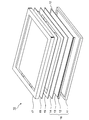
- FIG. 1 is an exploded perspective view showing a liquid crystal display device according to an embodiment of the present invention.
- the liquid crystal display device 10 is drawn in a state where it is placed horizontally so that the display surface faces upward.
- the liquid crystal display device 10 can be used as a television or computer display.
- the liquid crystal display device 10 includes a backlight chassis 11, a light source unit 12, a light guide plate 13, an optical sheet 14, a panel frame 15, a liquid crystal panel 16, and a bezel 17.
- An assembly of the backlight chassis 11, the light source units 12 and 12, the light guide plate 13, and the optical sheet 14 is referred to as a backlight device 18.
- the backlight chassis 11 is a box-shaped member that is a base for mounting (accommodating) each member of the backlight device 18 such as the light source unit 12, the light guide plate 13, and the optical sheet 14. It is desirable to use SECC (steel plate), Al, or the like as the material of the backlight chassis 11 in order to ensure rigidity and heat dissipation.
- SECC steel plate
- Al aluminum
- the light source unit 12 includes an LED (Light Emitting Diode) which is a point light source and an LED substrate on which the LED is mounted.
- LED Light Emitting Diode
- a plurality of LEDs are arranged along the one side of the light guide plate 13 at a predetermined interval on the LED substrate.
- the arrangement of the light source unit 12 employs an edge light system.
- a metal substrate such as Al is often used as an LED substrate in consideration of heat dissipation and strength.
- the two light source units 12 and 12 are provided along the opposite side surfaces of the light guide plate 13, but the light source unit 12 may be provided only along one side surface of the light guide plate 13.
- the configuration may also be provided along the other side surface of the light guide plate 13. That is, the light source unit 12 may be provided along at least one of the side surfaces of the light guide plate 13.
- the side faces the LED and serves as a light incident portion (light incident surface) that guides light from the LED into the light guide plate 13.
- the light guide plate 13 has a pair of main surfaces (upper surface and lower surface) and a plurality of side surfaces (four surfaces in FIG. 1) formed therebetween.
- the light guide plate 13 is a member that converts the LED light incident from its end face (side face) into a surface light source and derives it from the top face, and its material is acrylic, PC (polycarbonate), etc. from the viewpoint of thickness reduction and weight reduction. It is desirable to use this resin.
- the optical sheet 14 is a general term for a diffusion sheet, a lens sheet, a brightness enhancement sheet, and the like, and is a combination of any one or a plurality of these sheets. Since the optical sheet 14 is stacked on the light guide plate 13 to irradiate the liquid crystal panel 16 with uniform light, if the sheet has wrinkles or bends, the display quality deteriorates.
- the panel frame 15 is a frame-like member that holds the liquid crystal panel 16 so that the liquid crystal panel 16 and the optical sheet 14 do not contact each other, and it is desirable to use a resin such as PC as the material.
- the panel frame 15 also has a role of suppressing warping and bending of the optical sheet 14.
- the liquid crystal panel 16 is a member in which a liquid crystal element is injected between two transparent substrates, and the liquid crystal element is driven and illuminated by the backlight device 18 to display an image.
- the bezel 17 is a member that holds and holds the liquid crystal panel 16 in a frame shape, and covers the box-shaped backlight chassis 11 so as to cover it.
- the material may be PC, ABS resin, CFRP (carbon fiber reinforced plastics), etc. for weight reduction. For further weight reduction, these materials may be used to integrally form a casing (not shown) as an exterior and the bezel 17.
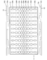
- FIG. 2 is a plan view of the light guide plate 13 and the light source unit 12 in the liquid crystal display device according to the first embodiment of the present invention.
- 21 is a light guide plate of the first embodiment which is an embodiment of the light guide plate 13
- 12a is an LED
- 12b is an LED substrate.
- a plurality of dots 22 for diffusing the light incident from the LED 12a is formed on the lower surface (back surface) of the light guide plate 21.
- the dot 22 should just be formed in at least one of the main surfaces of the light-guide plate 21.
- FIG. The dots referred to here are diffused by mainly reflecting the light in the light guide plate 21, and are formed by printing a white paint containing a small amount of scattering material or the like with an inkjet or the like. Reflection by the dots 22 does not occur on the entire surface, but only the vicinity of the outer periphery that is substantially perpendicular to the incident light becomes the reflection region, and the dot shape is designed based on this.
- the dots 22 are horizontally long elliptical first dots 22a arranged in the center of the light guide plate 21 (a portion on the straight line that is the same distance from the opposite light incident portion of the light guide plate 21) and the first dots 22a.
- the fourth dots 22d which are slightly vertically long and arranged in a straight line on the light incident part side of the third dot 22c, and the vertically long ellipses, which are lined in a straight line on the light incident part side of the fourth dot 22d, respectively.
- the fifth dot 22e may be provided in a plurality of rows according to the size of the light guide plate.
- the dots in the vicinity of the light incident part and the dots in the vicinity of the central part have substantially the same area.
- the dot near the light incident portion may be the fifth dot 22e
- the dot near the central portion may be the first dot 22a
- the dots near the light incident portion may be the fourth and fifth dots 22d and 22e, the center.
- the dots in the vicinity of the portion may be the first and second dots 22a and 22b.
- all of the first to fifth dots 22a to 22e have the same area. In this way, the printing area of each dot is substantially equal, and it is not necessary to form a dot that is too small, so printing is stabilized.
- the length in the direction substantially parallel to the light incident part of the dot near the center is substantially parallel to the light incident part of the dot near the light incident part. It should be longer than the length in the correct direction. Therefore, in the case of an elliptical dot having substantially the same area, for example, the dots in the vicinity of the central portion (for example, the first and second dots 22a and 22b) are horizontally long dots, and the dots in the vicinity of the light incident portion (for example, the fourth and second dots). 5 dots 22d and 22e) can be vertically long dots.
- each dot from the fifth dot 22e to the first dot 22a from the vicinity of the light incident portion to the vicinity of the central portion is gradually increased in length in a direction substantially parallel to the light incident portion. That is, a vertically long dot (fifth dot 22e), a slightly vertically long dot (fourth dot 22d), a circular dot (third dot 22c), a slightly horizontally long dot (second dot) from the light incident part toward the center part. 22b) and horizontally long dots (first dots 22a).
- the dots in the vicinity of the central portion and the dots in the vicinity of the light incident portion may have the same shape and be rotated by 90 °.
- the first dot 22a and the fifth dot 22e have the same shape and are rotated by 90 °
- the second dot 22b and the fourth dot 22d have the same shape and are rotated by 90 °. .
- the “near the central portion” can be a range of up to 50% of the length from the central portion to the light incident portion, for example, about 5% of the length from the central portion to the light incident portion. Or about 10%.
- the “near light incident portion” can be a range of up to 50% of the length from the light incident portion to the central portion, for example, about 5% of the length from the light incident portion to the central portion. It can be in the range of about 10%.
- each dot from the light incident portion toward the central portion is arranged in a straight line. That is, as shown in FIG. 2, the dots 22 are arranged in the vertical direction of the light guide plate 21.
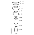
- FIG. 3 is a diagram illustrating a dot reflection area according to the first embodiment.
- the light incident direction is indicated by an arrow.
- the reflection regions 23a to 23e are elliptical regions that are in contact with a portion that is substantially parallel to the light incident portion of the outer peripheral portion on the central portion side of the light guide plate 31 in each dot. In other words, in each dot, only the vicinity of the outer periphery that is substantially perpendicular to the incident light is the reflection region.
- each dot do not become the entire surface of the dots, but a part of each dot becomes the reflection areas 23a to 23e in the light incident direction. Therefore, even if the size of each dot 22 is the same, changing the shape like the first to fifth dots 22a to 22e also changes the reflection area. Then, by adopting shapes such as the first to fifth dots 22a to 22e, the reflective area becomes smaller in order from the first reflective area 23a to the fifth reflective area 23e.
- each dot has a different reflection area as shown in FIG. 3, so the dots 22 are closer to the center of the light guide plate 21 than to the vicinity of the light incident portion. More light is reflected. Therefore, a small amount of light can be extracted in the vicinity of the light incident portion where the light from the light source is strong, and more light can be extracted near the central portion where the light from the light source is weak. As a result, the amount of light extracted in the vicinity of the central portion and the vicinity of the light incident portion is substantially equal, and a uniform surface light source can be obtained. Moreover, since the printing area of each dot is substantially equal and there are no dots that are too small, printing is stable and uniformity is stable. As a result, the production stability of the light guide plate 21 can be maintained.
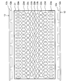
- FIG. 4 is a plan view of the light guide plate and the light source unit in the liquid crystal display device according to the second embodiment of the present invention.
- the dots of the first embodiment are arranged in a staggered pattern.
- symbol is attached
- the dots 22 from the light incident part to the central part are arranged in a staggered manner. Thereby, dots can be arranged densely and uniformity can be improved. Needless to say, the same effects as those of the first embodiment can be obtained.
- FIG. 5 is a plan view of the light guide plate and the light source unit in the liquid crystal display device according to the third embodiment of the present invention.
- the elliptical dots of the first embodiment are made substantially rectangular or square.
- symbol is attached
- the first, second, fourth, and fifth dots 42a, 42b, 42d, and 42e are substantially rectangular, and the third dot is substantially square. By rounding the corners of each dot 42, it is possible to prevent the reflected light from becoming strong at the corners.
- FIG. 6 is a diagram illustrating a dot reflection area according to the third embodiment.
- the light incident direction is indicated by an arrow.
- the first to fifth reflection regions 43a to 43e corresponding to the first to fifth dots 42a to 42e are regions that are in contact with a portion substantially parallel to the light incident portion of the outer peripheral portion on the center side of the light guide plate 41 in each dot. It is. In other words, in each dot, only the vicinity of the outer periphery that is substantially perpendicular to the incident light is the reflection region.
- the same effect as that of the first embodiment can be obtained even when a substantially rectangular or substantially square dot is used.
- the substantially rectangular or substantially square dots of the third embodiment may be arranged in a staggered manner as in the second embodiment. In this case, the same effect as the second embodiment can be obtained.
- the shape of the dot is not limited to the above-described substantially rectangular shape, substantially square shape, elliptical shape, or circular shape, and any other shape such as another polygonal shape or other curved shape may be employed. Moreover, you may change a shape for every dot.
- the present invention can be used for a light guide plate used for an edge light type backlight device, a backlight device including the light guide plate, and a liquid crystal display device, and is particularly suitable for a large liquid crystal display device such as a liquid crystal television. Can be used.
Landscapes
- Physics & Mathematics (AREA)
- General Physics & Mathematics (AREA)
- Optics & Photonics (AREA)
- Planar Illumination Modules (AREA)
Abstract
側面がLEDに対向する入光部である導光板において、下面に、LEDから入射した光を拡散させる複数のドットが形成され、入光部近傍のドットと下面の中央部近傍のドットとが略同面積であり、中央部近傍のドットの入光部と略平行な方向の長さが、入光部近傍のドットの前記入光部と略平行な方向の長さより長い構成とする。
Description
本発明は、エッジライト方式のバックライト装置に使用する導光板、その導光板を備えたバックライト装置及び液晶表示装置に関する。
現在、液晶テレビなどの大型の液晶表示装置に用いられているバックライト装置は、薄型化のためにエッジライト方式が採用されることが多い。このエッジライト方式のバックライト装置は、導光板と、導光板の側面に対向して配設されたLED等の光源と、導光板上に重ねられた拡散シートやレンズシート等の光学シートなどを備えている。そして、光源からの光は導光板に入光され、続いて光学シートに導かれて面光源に変換される。
また、エッジライト方式では光源近傍が高輝度になりやすく、均一な面光源を得るために様々な工夫が提案されている。その一つに、導光板の主面に光源から入射した光を拡散させる複数のドットを形成することでユニフォミティを得る手法が知られている。このドットは、白色を印刷することで形成される。
ここで、エッジライト方式を採用する大型の液晶表示装置の場合、導光板の光源の近傍において、ドットによる光取り出し量を著しく減少させる必要がある。したがって、導光板の光源近傍におけるドットを大幅に小さくする必要がある。しかし、ドットを大幅に小さくすると、印刷が安定しないためユニフォミティが安定せず、導光板の生産安定性が悪化するという問題が生じる。
特許文献1には、導光板、前記導光板の側面又は相対する2側面に配置された光源、前記導光板の上面に配置された拡散シート、前記拡散シートの上に配置された液晶表示素子、及び前記導光板の下面に配置された反射シートを備えた液晶表示装置であって、前記導光板の下面には、前記光源より該導光板に入射した光を該導光板の上面及び下面方向に拡散させるドットが形成され、前記導光板の下面の前記光源近傍に形成された複数のドットの内部には平滑面が各々形成され、且つ該光源近傍に形成された該ドット内の被覆率が60~80%であることを特徴とする液晶表示装置が開示されている。
しかしながら、特許文献1ではドットの内部に形成される平滑面は非印刷部分であるため、各ドットの印刷面積は小さくなっている。その結果、印刷が不安定になってユニフォミティが安定せず、導光板の生産安定性は悪化する。
本発明は、ドットを工夫することによりユニフォミティを安定させ、生産安定性を保つことができる導光板を提供することを目的とする。また、その導光板を備えたバックライト装置を提供することも目的とする。また、そのバックライト装置を備えた液晶表示装置を提供することも目的とする。
上記目的を達成するために本発明は、一対の主面とその間に形成された複数の側面とを有し、該側面の少なくとも1つが光源に対向する入光部である導光板において、前記主面の少なくとも一方に、前記光源から入射した光を拡散させる複数のドットが形成され、前記入光部近傍のドットと前記主面の中央部近傍のドットとが略同面積であり、前記中央部近傍のドットの前記入光部と略平行な方向の長さが、入光部近傍のドットの前記入光部と略平行な方向の長さより長いことを特徴とする。
本発明によると、導光板のドットの面積を小さくせずにドットの形状を変えることで各ドットが有する反射領域を制御しているので、ドットの形成が安定する。その結果、ユニフォミティが安定し、生産安定性を保つことができる。
以下に本発明の実施形態を図面を参照して説明する。
図1は、本発明の一実施形態の液晶表示装置を示す分解斜視図である。図1において液晶表示装置10は、表示面が上向きになるように水平に置かれた状態で描かれている。
この液晶表示装置10は、テレビやコンピュータのディスプレイとして利用できる。液晶表示装置10は、バックライトシャーシ11と、光源ユニット12と、導光板13と、光学シート14と、パネルフレーム15と、液晶パネル16と、ベゼル17とを備えている。そして、バックライトシャーシ11と、光源ユニット12、12と、導光板13と、光学シート14とを組み立てたものをバックライト装置18と称する。
バックライトシャーシ11は、光源ユニット12、導光板13、光学シート14などのバックライト装置18の各部材を搭載(収容)するための土台となる部材であり箱形である。バックライトシャーシ11の材料には、剛性及び放熱性を確保するため、SECC(鋼板)やAlなどを用いることが望ましい。
光源ユニット12は、点状光源であるLED(Light Emitting Diode)と、LEDを搭載するLED基板とを含んでいる。なお、光源としては、LEDの他に線状光源である蛍光管などを用いてもよい。そして、LED基板上で複数のLEDが導光板13の一辺に沿って所定間隔で配設されている。光源ユニット12の配置は、エッジライト方式を採用している。大型の液晶表示装置においては、LED基板として放熱性や強度を考慮してAlなどの金属基板を用いることが多い。
また、光源ユニット12をバックライトシャーシ11に固定する固定手段としては、ネジや粘着剤を用いることができる。また、図1では2つの光源ユニット12、12がそれぞれ導光板13の対向する側面に沿って設けられているが、導光板13の一側面に沿ってのみ光源ユニット12を設ける構成としてもよいし、導光板13の他の側面に沿っても設ける構成としてもよい。つまり、光源ユニット12は導光板13の側面の少なくとも1つに沿って設ける構成とすればよい。ここで、側面はLEDに対向し、LEDからの光を導光板13内へ導く入光部(入光面)となる。
導光板13は、一対の主面(上面及び下面)とその間に形成された複数の側面(図1では4面)とを有する。導光板13は、その端面(側面)から入射したLEDの光を面光源へ変換して上面から導出する部材であり、その材料としては薄型化、軽量化の観点からアクリルやPC(ポリカーボネート)などの樹脂を用いることが望ましい。
光学シート14は、拡散シート、レンズシート、輝度向上シート等の総称であり、これらのシートの何れか1枚又は複数枚を組み合わせたものである。光学シート14は導光板13上に重ねられ、液晶パネル16に均一な光を照射するためのものであるので、シートに皺や撓みがあると表示品位の悪化原因となる。
パネルフレーム15は、液晶パネル16と光学シート14とが接触しないように液晶パネル16を保持する額縁状の部材であり、その材料としてはPCなどの樹脂を用いることが望ましい。また、パネルフレーム15には光学シート14の反りや撓みを抑制する役割もある。
液晶パネル16は、2枚の透明基板の間に液晶素子が注入された部材であり、液晶素子が駆動され、バックライト装置18により照明されることで映像を表示する。
ベゼル17は、額縁状で液晶パネル16を押さえて固定する部材であり、箱形のバックライトシャーシ11に蓋をするように被せられる。その材料としてはSECCやAlなどの他、軽量化のためにPC、ABS樹脂、CFRP((carbon fiber reinforced plastics)炭素繊維強化プラスチック)などを用いてもよい。さらなる軽量化のためには、これらの材料を用い、外装となる筐体(不図示)とベゼル17とを一体成形してもよい。
以下、このような液晶表示装置10における本発明の特徴的な構成である導光板13の実施形態について詳しく説明する。
<第1実施形態>
図2は、本発明の第1実施形態の液晶表示装置における導光板13及び光源ユニット12の平面図である。図2において、21は導光板13の一実施形態である第1実施形態の導光板、12aはLED、12bはLED基板である。
図2は、本発明の第1実施形態の液晶表示装置における導光板13及び光源ユニット12の平面図である。図2において、21は導光板13の一実施形態である第1実施形態の導光板、12aはLED、12bはLED基板である。
導光板21の下面(裏面)に、LED12aから入射した光を拡散させる複数のドット22が形成されている。なお、ドット22は導光板21の主面の少なくとも一方に形成されていればよい。ここで言うドットとは、導光板21内の光を主に反射させることで拡散させるものであり、微量の散乱材等を含んだ白色の塗料をインクジェット等で印刷することで形成される。ドット22での反射は全面で生じるのではなく、入光に対して略垂直な外周付近のみが反射領域となるため、これに基づいてドットの形状を設計する。
ドット22は、導光板21の中央部(導光板21の対向する入光部から同距離の部分であり直線上の部分)に並んだ横長の楕円形の第1ドット22aと、第1ドット22aの両側(入光部側)にそれぞれ直線状に並んだやや横長の楕円形の第2ドット22bと、第2ドット22bの入光部側にそれぞれ直線状に並んだ円形の第3ドット22cと、第3ドット22cの入光部側にそれぞれ直線状に並んだやや縦長の楕円形の第4ドット22dと、第4ドット22dの入光部側にそれぞれ直線状に並んだ縦長の楕円形の第5ドット22eと、で構成されている。なお、第1~第5ドット22a~22eは導光板の大きさに合わせてそれぞれ複数列設けてもよい。
また本実施形態では、少なくとも入光部近傍のドットと中央部近傍のドットとを略同面積とする。例えば、入光部近傍のドットとは第5ドット22e、中央部近傍のドットとは第1ドット22aとしてもよいし、入光部近傍のドットとは第4及び第5ドット22d、22e、中央部近傍のドットとは第1及び第2ドット22a、22bとしてもよい。なお、図2では第1~第5ドット22a~22e全てが同面積となっている。このように、各ドットの印刷面積がほぼ等しく、小さすぎるドットを形成する必要がないので、印刷が安定する。
また本実施形態では、少なくとも中央部近傍のドットの入光部と略平行な方向(図2の矢印方向(横方向))の長さが、入光部近傍のドットの入光部と略平行な方向の長さより長くなるようにする。よって、略同面積の楕円形のドットの場合、例えば、中央部近傍のドット(例えば第1及び第2ドット22a、22b)を横長のドットとし、入光部近傍のドット(例えば第4及び第5ドット22d、22e)を縦長のドットとすることができる。
さらに図2では、入光部近傍から中央部近傍へ向かう各ドット(第5ドット22eから第1ドット22a)は、入光部と略平行な方向の長さが徐々に長くなっている。つまり、入光部から中央部へ向かって縦長のドット(第5ドット22e)、やや縦長のドット(第4ドット22d)、円形のドット(第3ドット22c)、やや横長のドット(第2ドット22b)、横長のドット(第1ドット22a)の順に並んでいる。
例えば、中央部近傍のドットと入光部近傍のドットとは同形状で90°回転させて配置したものとすることができる。図2では、第1ドット22aと第5ドット22eとが同形状で90°回転させた関係にあり、また第2ドット22bと第4ドット22dとが同形状で90°回転させた関係にある。
ここで、「中央部近傍」とは、最大で中央部から入光部までの長さの50%の範囲とすることができ、例えば、中央部から入光部までの長さの約5%や約10%の範囲とすることができる。また「入光部近傍」とは、最大で入光部から中央部までの長さの50%の範囲とすることができ、例えば、入光部から中央部までの長さの約5%や約10%の範囲とすることができる。
また本実施形態では、入光部から中央部へ向かう各ドットは、直線状に配置される。つまり、図2に示すように、導光板21の縦方向にドット22が並べられる。
図3は、第1実施形態のドットの反射領域を説明する図である。図3において入光方向を矢印で示している。第1~第5ドット22a~22eにそれぞれ対応する第1~第5反射領域23a~23eは、各ドットにおいて導光板31の中央部寄りに生じる。具体的には、反射領域23a~23eは各ドットにおける導光板31の中央部側の外周部の入光部に略平行な部分に接する楕円形の領域である。換言すれば、各ドットにおいて入光に対して略垂直な外周付近のみが反射領域となる。
このように、各ドットの反射領域23a~23eは、ドット全面とはならず、入光方向に対して各ドットの一部が反射領域23a~23eとなる。したがって、各ドット22のサイズが同じであっても、第1~第5ドット22a~22eのように形状を変えることで、反射領域も変わる。そして、第1~第5ドット22a~22eのような形状とすることにより、第1反射領域23aから第5反射領域23eへ向かって順に反射領域が小さくなる。
したがって、本実施形態のようなドット22の配置によれば、各ドットは図3に示したような異なる反射領域をもつので、導光板21の中央部近傍では入光部近傍よりもドット22でより多くの光が反射する。よって、光源からの光が強い入光部近傍では少量の光を取り出し、光源からの光が弱い中央部付近でより多くの光を取り出すことができる。その結果、中央部付近と入光部付近とで取り出される光量がほぼ等しくなり、均一な面光源が得られる。また、各ドットの印刷面積が略等しく、小さすぎるドットがないため、印刷が安定し、ユニフォミティが安定する。その結果、導光板21の生産安定性を保つことができる。
<第2実施形態>
図4は、本発明の第2実施形態の液晶表示装置における導光板及び光源ユニットの平面図である。第2実施形態は、第1実施形態のドットを千鳥状に配置したものである。その他、第1実施形態と同様の構成には同符号を付し、その詳細な説明を省略する。
図4は、本発明の第2実施形態の液晶表示装置における導光板及び光源ユニットの平面図である。第2実施形態は、第1実施形態のドットを千鳥状に配置したものである。その他、第1実施形態と同様の構成には同符号を付し、その詳細な説明を省略する。
図4に示すように、導光板31においては、入光部から中央部へ向かう各ドット22が千鳥状に配置されている。これによりドットを密に配置でき、ユニフォミティを向上させることができる。なお、第1実施形態と同様の効果も得られることは言うまでもない。
<第3実施形態>
図5は、本発明の第3実施形態の液晶表示装置における導光板及び光源ユニットの平面図である。第3実施形態は、第1実施形態の楕円のドットを略長方形又は略正方形にしたものである。その他、第1実施形態と同様の構成には同符号を付し、その詳細な説明を省略する。
図5は、本発明の第3実施形態の液晶表示装置における導光板及び光源ユニットの平面図である。第3実施形態は、第1実施形態の楕円のドットを略長方形又は略正方形にしたものである。その他、第1実施形態と同様の構成には同符号を付し、その詳細な説明を省略する。
図5に示すように、導光板41においては、第1、第2、第4、第5ドット42a、42b、42d、42eが略長方形、第3ドットが略正方形となっている。各ドット42の角は丸く面取りされることで、角で反射光が強くなることを防止できる。
図6は、第3実施形態のドットの反射領域を説明する図である。図6において入光方向を矢印で示している。第1~第5ドット42a~42eにそれぞれ対応する第1~第5反射領域43a~43eは、各ドットにおける導光板41の中央部側の外周部の入光部に略平行な部分に接する領域である。換言すれば、各ドットにおいて入光に対して略垂直な外周付近のみが反射領域となる。
このように、略長方形又は略正方形のドットを用いても第1実施形態と同様の効果がえられる。なお、第3実施形態の略長方形又は略正方形のドットを第2実施形態のように千鳥状に配置してもよい。この場合、第2実施形態と同様の効果が得られる。
なお本発明において、ドットの形状は上述した略長方形又は略正方形、楕円形又は円形に限定されることはなく、他の多角形、他の曲形状など任意の形状を採用することもできる。また、ドット毎に形状を変えてもよい。
本発明は、エッジライト方式のバックライト装置に使用する導光板、その導光板を備えたバックライト装置及び液晶表示装置に利用することができ、特に液晶テレビなどの大型の液晶表示装置に好適に利用することができる。
10 液晶表示装置
11 バックライトシャーシ
12 光源ユニット
12a LED
12b LED基板
13、21、31、41 導光板
14 光学シート
15 パネルフレーム
16 液晶パネル
17 ベゼル
18 バックライト装置
22、42 ドット
23、43 反射領域
11 バックライトシャーシ
12 光源ユニット
12a LED
12b LED基板
13、21、31、41 導光板
14 光学シート
15 パネルフレーム
16 液晶パネル
17 ベゼル
18 バックライト装置
22、42 ドット
23、43 反射領域
Claims (8)
- 一対の主面とその間に形成された複数の側面とを有し、該側面の少なくとも1つが光源に対向する入光部である導光板において、
前記主面の少なくとも一方に、前記光源から入射した光を拡散させる複数のドットが形成され、
前記入光部近傍のドットと前記主面の中央部近傍のドットとが略同面積であり、
前記中央部近傍のドットの前記入光部と略平行な方向の長さが、入光部近傍のドットの前記入光部と略平行な方向の長さより長いことを特徴とする導光板。 - 前記入光部近傍から前記中央部近傍へ向かう各ドットは、前記入光部と略平行な方向の長さが徐々に長くなっていることを特徴とする請求項1記載の導光板。
- 前記ドットが楕円形又は円形であることを特徴とする請求項1又は2記載の導光板。
- 前記ドットが略長方形又は略正方形であることを特徴とする請求項1又は2記載の導光板。
- 前記入光部から前記中央部へ向かう各ドットは、直線状に配置されることを特徴とする請求項1~4の何れかに記載の導光板。
- 前記入光部から前記中央部へ向かう各ドットは、千鳥状に配置されることを特徴とする請求項1~4の何れかに記載の導光板。
- 請求項1~6の何れかに記載の導光板と、前記導光板へ発光する光源と、各部材を収容するバックライトシャーシとを備えたバックライト装置。
- 請求項7記載のバックライト装置と、該バックライト装置により照明される液晶パネルとを備えた液晶表示装置。
Applications Claiming Priority (2)
| Application Number | Priority Date | Filing Date | Title |
|---|---|---|---|
| JP2012234366 | 2012-10-24 | ||
| JP2012-234366 | 2012-10-24 |
Publications (1)
| Publication Number | Publication Date |
|---|---|
| WO2014065178A1 true WO2014065178A1 (ja) | 2014-05-01 |
Family
ID=50544558
Family Applications (1)
| Application Number | Title | Priority Date | Filing Date |
|---|---|---|---|
| PCT/JP2013/078129 Ceased WO2014065178A1 (ja) | 2012-10-24 | 2013-10-17 | 導光板、バックライト装置及び液晶表示装置 |
Country Status (1)
| Country | Link |
|---|---|
| WO (1) | WO2014065178A1 (ja) |
Cited By (1)
| Publication number | Priority date | Publication date | Assignee | Title |
|---|---|---|---|---|
| CN115735081A (zh) * | 2020-06-29 | 2023-03-03 | 西铁城电子株式会社 | 发光装置 |
Citations (4)
| Publication number | Priority date | Publication date | Assignee | Title |
|---|---|---|---|---|
| JPH08271893A (ja) * | 1995-03-31 | 1996-10-18 | Enplas Corp | サイドライト型面光源装置 |
| JP2008516391A (ja) * | 2004-10-09 | 2008-05-15 | チェイル インダストリーズ インコーポレイテッド | 液晶表示装置バックライトユニット用導光板及びこれを用いた液晶表示装置用バックライトユニット |
| US7403691B2 (en) * | 2004-12-21 | 2008-07-22 | Hon Hai Precision Industry Co., Ltd. | Light guide plate having high-density dots |
| JP2012185275A (ja) * | 2011-03-04 | 2012-09-27 | Toshiba Corp | バックライト装置および表示装置 |
-
2013
- 2013-10-17 WO PCT/JP2013/078129 patent/WO2014065178A1/ja not_active Ceased
Patent Citations (4)
| Publication number | Priority date | Publication date | Assignee | Title |
|---|---|---|---|---|
| JPH08271893A (ja) * | 1995-03-31 | 1996-10-18 | Enplas Corp | サイドライト型面光源装置 |
| JP2008516391A (ja) * | 2004-10-09 | 2008-05-15 | チェイル インダストリーズ インコーポレイテッド | 液晶表示装置バックライトユニット用導光板及びこれを用いた液晶表示装置用バックライトユニット |
| US7403691B2 (en) * | 2004-12-21 | 2008-07-22 | Hon Hai Precision Industry Co., Ltd. | Light guide plate having high-density dots |
| JP2012185275A (ja) * | 2011-03-04 | 2012-09-27 | Toshiba Corp | バックライト装置および表示装置 |
Cited By (1)
| Publication number | Priority date | Publication date | Assignee | Title |
|---|---|---|---|---|
| CN115735081A (zh) * | 2020-06-29 | 2023-03-03 | 西铁城电子株式会社 | 发光装置 |
Similar Documents
| Publication | Publication Date | Title |
|---|---|---|
| US9354385B2 (en) | Curved display apparatus | |
| US9223074B2 (en) | Light guide plate and area light source device | |
| CN100474073C (zh) | 显示装置 | |
| US9746602B2 (en) | Backlight device and display device including the same | |
| CN102661527B (zh) | 背光模组及液晶显示器 | |
| US20090267889A1 (en) | Display device | |
| US9810934B2 (en) | Display device | |
| US20090167641A1 (en) | Optical Plate, Backlight Assembly and Display Device Including the Same | |
| US9810935B2 (en) | Display device | |
| KR20100119679A (ko) | 액정 표시 장치 | |
| US9841553B2 (en) | Display device having adhesive framing member for optical sheets | |
| WO2012133312A1 (ja) | バックライトユニット | |
| CN102287682A (zh) | 背光单元和显示装置 | |
| JP2011216322A (ja) | 発光装置およびこれを用いた表示装置 | |
| US20180157115A1 (en) | Edge-lit backlight device and liquid crystal display device | |
| US20120320623A1 (en) | Illuminating device and display device | |
| JP2010108601A (ja) | 面状光源及び液晶表示装置 | |
| US20150146136A1 (en) | Side-light type backlight module | |
| US20140043858A1 (en) | Light guide plate and display device having the same | |
| WO2014065178A1 (ja) | 導光板、バックライト装置及び液晶表示装置 | |
| WO2013005554A1 (ja) | 光学シート、バックライト装置及び液晶表示装置 | |
| WO2014199676A1 (ja) | 導光体及びそれを備えた面状発光装置 | |
| KR20130091227A (ko) | 백라이트 유닛용 지지부재, 이를 구비한 백라이트 유닛 및 영상 표시 장치 | |
| JP5814827B2 (ja) | 光源モジュール、及び、液晶表示装置 | |
| US9028126B2 (en) | LED light bar and side-edge backlight module using same |
Legal Events
| Date | Code | Title | Description |
|---|---|---|---|
| 121 | Ep: the epo has been informed by wipo that ep was designated in this application |
Ref document number: 13849164 Country of ref document: EP Kind code of ref document: A1 |
|
| NENP | Non-entry into the national phase |
Ref country code: DE |
|
| 122 | Ep: pct application non-entry in european phase |
Ref document number: 13849164 Country of ref document: EP Kind code of ref document: A1 |
|
| NENP | Non-entry into the national phase |
Ref country code: JP |