WO2014054271A1 - 出力装置、太陽光発電装置および太陽光発電出力方法 - Google Patents
出力装置、太陽光発電装置および太陽光発電出力方法 Download PDFInfo
- Publication number
- WO2014054271A1 WO2014054271A1 PCT/JP2013/005841 JP2013005841W WO2014054271A1 WO 2014054271 A1 WO2014054271 A1 WO 2014054271A1 JP 2013005841 W JP2013005841 W JP 2013005841W WO 2014054271 A1 WO2014054271 A1 WO 2014054271A1
- Authority
- WO
- WIPO (PCT)
- Prior art keywords
- signal
- photoelectric conversion
- output
- converter
- conversion cells
- Prior art date
- Legal status (The legal status is an assumption and is not a legal conclusion. Google has not performed a legal analysis and makes no representation as to the accuracy of the status listed.)
- Ceased
Links
Images





Classifications
-
- H—ELECTRICITY
- H02—GENERATION; CONVERSION OR DISTRIBUTION OF ELECTRIC POWER
- H02J—ELECTRIC POWER NETWORKS; CIRCUIT ARRANGEMENTS OR SYSTEMS FOR SUPPLYING OR DISTRIBUTING ELECTRIC POWER; SYSTEMS FOR STORING ELECTRIC ENERGY
- H02J3/00—Circuit arrangements for AC mains or AC distribution networks
- H02J3/38—Arrangements for feeding a single network from two or more generators or sources in parallel; Arrangements for feeding already energised networks from additional generators or sources in parallel
- H02J3/381—Dispersed generators
-
- H—ELECTRICITY
- H02—GENERATION; CONVERSION OR DISTRIBUTION OF ELECTRIC POWER
- H02S—GENERATION OF ELECTRIC POWER BY CONVERSION OF INFRARED RADIATION, VISIBLE LIGHT OR ULTRAVIOLET LIGHT, e.g. USING PHOTOVOLTAIC [PV] MODULES
- H02S10/00—PV power plants; Combinations of PV energy systems with other systems for the generation of electric power
-
- H—ELECTRICITY
- H02—GENERATION; CONVERSION OR DISTRIBUTION OF ELECTRIC POWER
- H02S—GENERATION OF ELECTRIC POWER BY CONVERSION OF INFRARED RADIATION, VISIBLE LIGHT OR ULTRAVIOLET LIGHT, e.g. USING PHOTOVOLTAIC [PV] MODULES
- H02S40/00—Components or accessories in combination with PV modules, not provided for in groups H02S10/00 - H02S30/00
- H02S40/20—Optical components
- H02S40/22—Light-reflecting or light-concentrating means
-
- H—ELECTRICITY
- H02—GENERATION; CONVERSION OR DISTRIBUTION OF ELECTRIC POWER
- H02S—GENERATION OF ELECTRIC POWER BY CONVERSION OF INFRARED RADIATION, VISIBLE LIGHT OR ULTRAVIOLET LIGHT, e.g. USING PHOTOVOLTAIC [PV] MODULES
- H02S40/00—Components or accessories in combination with PV modules, not provided for in groups H02S10/00 - H02S30/00
- H02S40/30—Electrical components
- H02S40/34—Electrical components comprising specially adapted electrical connection means to be structurally associated with the PV module, e.g. junction boxes
-
- H—ELECTRICITY
- H10—SEMICONDUCTOR DEVICES; ELECTRIC SOLID-STATE DEVICES NOT OTHERWISE PROVIDED FOR
- H10F—INORGANIC SEMICONDUCTOR DEVICES SENSITIVE TO INFRARED RADIATION, LIGHT, ELECTROMAGNETIC RADIATION OF SHORTER WAVELENGTH OR CORPUSCULAR RADIATION
- H10F77/00—Constructional details of devices covered by this subclass
- H10F77/40—Optical elements or arrangements
- H10F77/42—Optical elements or arrangements directly associated or integrated with photovoltaic cells, e.g. light-reflecting means or light-concentrating means
- H10F77/492—Spectrum-splitting means, e.g. dichroic mirrors
-
- H—ELECTRICITY
- H02—GENERATION; CONVERSION OR DISTRIBUTION OF ELECTRIC POWER
- H02J—ELECTRIC POWER NETWORKS; CIRCUIT ARRANGEMENTS OR SYSTEMS FOR SUPPLYING OR DISTRIBUTING ELECTRIC POWER; SYSTEMS FOR STORING ELECTRIC ENERGY
- H02J2101/00—Supply or distribution of decentralised, dispersed or local electric power generation
- H02J2101/20—Dispersed power generation using renewable energy sources
- H02J2101/22—Solar energy
- H02J2101/24—Photovoltaics
- H02J2101/25—Photovoltaics involving maximum power point tracking control for photovoltaic sources
-
- Y—GENERAL TAGGING OF NEW TECHNOLOGICAL DEVELOPMENTS; GENERAL TAGGING OF CROSS-SECTIONAL TECHNOLOGIES SPANNING OVER SEVERAL SECTIONS OF THE IPC; TECHNICAL SUBJECTS COVERED BY FORMER USPC CROSS-REFERENCE ART COLLECTIONS [XRACs] AND DIGESTS
- Y02—TECHNOLOGIES OR APPLICATIONS FOR MITIGATION OR ADAPTATION AGAINST CLIMATE CHANGE
- Y02E—REDUCTION OF GREENHOUSE GAS [GHG] EMISSIONS, RELATED TO ENERGY GENERATION, TRANSMISSION OR DISTRIBUTION
- Y02E10/00—Energy generation through renewable energy sources
- Y02E10/50—Photovoltaic [PV] energy
- Y02E10/52—PV systems with concentrators
-
- Y—GENERAL TAGGING OF NEW TECHNOLOGICAL DEVELOPMENTS; GENERAL TAGGING OF CROSS-SECTIONAL TECHNOLOGIES SPANNING OVER SEVERAL SECTIONS OF THE IPC; TECHNICAL SUBJECTS COVERED BY FORMER USPC CROSS-REFERENCE ART COLLECTIONS [XRACs] AND DIGESTS
- Y02—TECHNOLOGIES OR APPLICATIONS FOR MITIGATION OR ADAPTATION AGAINST CLIMATE CHANGE
- Y02E—REDUCTION OF GREENHOUSE GAS [GHG] EMISSIONS, RELATED TO ENERGY GENERATION, TRANSMISSION OR DISTRIBUTION
- Y02E10/00—Energy generation through renewable energy sources
- Y02E10/50—Photovoltaic [PV] energy
- Y02E10/56—Power conversion systems, e.g. maximum power point trackers
Definitions
- the present invention relates to a technology related to power generation using sunlight.
- FIG. 9 is a diagram illustrating an example of a solar power generation device.
- This solar power generation device is a concentrating stacked solar power generation device.
- the solar power generation device includes a condenser lens 20B, a stacked photoelectric conversion cell 17, and an output device (power converter) 14D.
- the stacked photoelectric conversion cell 17 includes a plurality of photoelectric conversion cells 2, 3, 4 and electrodes 15, 16.
- the photoelectric conversion cells 2 to 4, the electrodes 15 and 16, and the condenser lens 20B are represented by a cross-sectional view along the optical axis 23 of the condenser lens 20B.
- the condensing lens 20 ⁇ / b> B is a lens that condenses sunlight incident in parallel with the optical axis 23.
- Each of the photoelectric conversion cells 2 to 4 has a function of converting light (sunlight) into electricity.
- the sensitivity wavelength bands of the photoelectric conversion cells 2 to 4 are different from each other.
- These photoelectric conversion cells 2 to 4 are stacked and electrically connected in series.
- the electrodes 15 and 16 are respectively connected to both ends of the connection circuit in which the photoelectric conversion cells 2 to 4 are connected in series.
- the light receiving surface is perpendicular to the optical axis 23 of the condensing lens 20B, and the light receiving surface is the condensing lens 20B. It is arranged so as to be a focal position.
- the output device (power converter) 14D converts electric energy from the photoelectric conversion cells 2 to 4 output from the electrodes 15 and 16 into electric power having a predetermined electric characteristic (for example, a voltage having a predetermined voltage value, a predetermined voltage value, An electric circuit for converting the current into a current having a current value.
- a predetermined electric characteristic for example, a voltage having a predetermined voltage value, a predetermined voltage value, An electric circuit for converting the current into a current having a current value.
- the above-described concentrating type solar power generation apparatus has a problem that it is difficult to further improve efficiency. That is, the stacked photoelectric conversion cell 17 has a structure in which sunlight passes through the photoelectric conversion cells 2 to 4 in order, so that the sunlight is attenuated as it passes through the photoelectric conversion cells 2 to 4. For this reason, the power generation amount in the lower photoelectric conversion cell 4 is smaller than that in the upper photoelectric conversion cell 2.
- the inventor has proposed various technologies related to a solar power generation device, and one of them is a solar power generation device that takes such problems into consideration (see, for example, Patent Document 1).
- the photoelectric conversion cells 2 to 4 are connected in series as described above. For this reason, the electrical resistance of the photoelectric conversion cells 2 to 4 is increased due to the electrical resistance at the connection portion (cell boundary portion), and the energization amount of the photoelectric conversion cells 2 to 4 is suppressed. Further, the photoelectric conversion cells 2 to 4 having different sensitivity wavelength bands often have different internal resistances. When the photoelectric conversion cells 2 to 4 having different internal resistances are connected in series, the energization amount of the photoelectric conversion cells 2 to 4 is limited by the largest internal resistance among the internal resistances of the photoelectric conversion cells 2 to 4. This causes a problem that the electric power generated by the photoelectric conversion cells 2 to 4 cannot be sufficiently output.
- the present inventor has realized that there is a problem that the photovoltaic power generation apparatus cannot output power efficiently due to the configuration related to the output of electric energy, including the above problems. .
- the main object of the present invention is to provide a technique that can efficiently output the electric power generated by the photoelectric conversion cell at low cost.
- the output device of the present invention is A plurality of converters connected to each of a plurality of types of photoelectric conversion cells having different sensitivity wavelength bands, and having a function of converting power output from the connected photoelectric conversion cells; Based on the output power output from at least one of the plurality of types of photoelectric conversion cells, the plurality of converters so that the power output from the photoelectric conversion cell that is the output source of the output power becomes the maximum power point.
- a control device that generates a basic signal that is a basis of a plurality of control signals that respectively control
- a signal adjusting device that multiplies the basic signal by a constant and supplies the signal multiplied by the constant as the control signal to the converter that is a signal supply partner.
- the solar power generation device of the present invention is A plurality of types of photoelectric conversion cells having different sensitivity wavelength bands;
- the output device of the present invention is provided.
- the photovoltaic power generation output method of the present invention includes: Based on output power output from at least one of a plurality of types of photoelectric conversion cells having different sensitivity wavelength bands, the power output from the photoelectric conversion cell that is the output source of the output power becomes the maximum power point. So as to generate a basic signal as a basis for a plurality of control signals for controlling a plurality of converters respectively connected to the plurality of types of photoelectric conversion cells, The basic signal is multiplied by a constant, and the signal multiplied by a constant is supplied to the converter as a signal supply partner as the control signal, The converter operates based on the control signal to convert and output the power output from the photoelectric conversion cell.
- the electric power generated by the photoelectric conversion cell can be efficiently output at low cost.
- FIG. 6 is a circuit diagram illustrating another circuit configuration example of the DC-DC converter.
- FIG. 1 is a model diagram showing a simplified configuration of an output device according to a first embodiment of the present invention and a solar power generation device including the output device.
- the solar power generation device according to the first embodiment includes a plurality of types of photoelectric conversion cells 2, 3, and 4 and an output device 14A.
- the photoelectric conversion cells 2 to 4 have a function of converting light (solar energy) into electric energy.
- the sensitivity wavelength bands of the photoelectric conversion cells 2 to 4 are different from each other. These photoelectric conversion cells 2 to 4 are electrically separated from each other.
- the output device 14 ⁇ / b> A includes a plurality of converters 5, 6, 7, a control device 8, and signal adjustment devices 9, 10.
- the converter 5 is connected to the photoelectric conversion cell 2, the converter 6 is connected to the photoelectric conversion cell 3, and the converter 7 is connected to the photoelectric conversion cell 4. That is, each of the converters 5 to 7 is connected to one different type of photoelectric conversion cell among the plurality of types of photoelectric conversion cells 2 to 4.
- the converters 5 to 7 are power having a predetermined electrical characteristic (for example, a voltage having a predetermined voltage value or a current having a predetermined current value) that is output from the connected photoelectric conversion cells 2 to 4. It has the function to convert to.
- the control device 8 has a function of generating a basic signal based on power output from at least one of the plurality of types of photoelectric conversion cells 2 to 4.
- the basic signal is a plurality of control signals for controlling the converters 5 to 7 so that the power output from the photoelectric conversion cells 2 to 4 becomes the maximum power point (MPP (Maximum Power Point)) of the photoelectric conversion cells 2 to 4. This is the signal that is the basis of.
- MPP Maximum Power Point
- the control device 8 controls the converter 7 so that the power output from the photoelectric conversion cell 4 becomes the maximum power point of the photoelectric conversion cell 4 based on the power output from the photoelectric conversion cell 4 ( Control signal) as a basic signal.
- the signal conditioners 9 and 10 multiply the basic signal by a constant, and supply the signal multiplied by the constant to the converter 5 or the converter 6 that is a signal supply partner as a control signal.
- the signal adjustment device 9 multiplies the basic signal by a constant, and supplies the signal multiplied by the constant to the converter 5 as a control signal.
- the constant multiplied by the basic signal is connected to, for example, the characteristic value of the photoelectric conversion cell 4 that is the output source of power used when the control device 8 generates the basic signal, and the converter 5 (signal supply partner). It is a constant corresponding to the ratio to the characteristic value of the photoelectric conversion cell 2.
- the signal adjustment device 10 multiplies the basic signal by a constant, and supplies the signal multiplied by the constant to the converter 6 as a control signal.
- the constant multiplied by the basic signal is connected to, for example, the characteristic value of the photoelectric conversion cell 4 that is the output source of power used when the control device 8 generates the basic signal, and the converter 6 (signal supply partner). It is a constant corresponding to the ratio with the characteristic value of the photoelectric conversion cell 3. In the example shown in FIG. 1, since the basic signal generated by the control device 8 is supplied as it is to the converter 7 as a control signal, the signal adjustment device similar to the above corresponding to the converter 7 is not installed.
- the solar power generation apparatus can obtain the following effects. That is, in the first embodiment, the plurality of photoelectric conversion cells 2 to 4 are separated from each other, and power is output for each of the photoelectric conversion cells 2 to 4 (power is taken out). For this reason, the problem which arises when taking out electric power from the several photoelectric conversion cell electrically connected in series as mentioned above can be prevented. That is, the solar power generation device of this 1st Embodiment can prevent the power loss in the connection (boundary) part of a photoelectric conversion cell. And the said solar power generation device can prevent the problem that the electric current which flows into a photoelectric conversion cell is restrict
- the control device 8 of the output device 14A generates a signal for controlling the converters 5 to 7 so that the power of the photoelectric conversion cells 2 to 4 becomes the maximum power point as described above. It has a function. In other words, the control device 8 has a function as a maximum power point tracking device.
- the output device 14A of the first embodiment does not require such a complex maximum power point tracking device (control device 8) for each of the converters 5-7. The effect that it is finished can be acquired. Thereby, 14 A of output devices and a solar power generation device provided with the same can aim at simplification of composition. Further, the output device 14A and the solar power generation device including the output device 14A can reduce the cost.
- the output device 14A of the first embodiment and the solar power generation apparatus including the output device 14A can obtain an effect of efficiently outputting the electric power generated by the photoelectric conversion cells 2 to 4 at low cost.
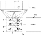
- FIG. 2 is a model diagram showing a simplified configuration of the photovoltaic power generation apparatus according to the second embodiment of the present invention.
- the solar power generation device according to the second embodiment includes a condenser lens 20A, a photoelectric unit 21, and an output device 14B.
- the condenser lens 20A and the photoelectric unit 21 are represented by a cross section along the optical axis 23 of the condenser lens 20A.
- the condensing lens 20A has a function of condensing light (sunlight) incident in parallel to the optical axis 23 of the condensing lens 20A and a spectral decomposition function.
- the cross section of the condensing lens 20A is similar to the portion of the cross section of the condensing lens 20B shown in FIG. 9 excluding the region 26 having the radius R from the optical axis 23.
- the condensing lens 20 ⁇ / b> A forms a ring-shaped focal point with a radius R around the optical axis 23.
- the condensing lens 20A focuses on each wavelength band at a position shifted in a direction away from the condensing lens 20A as the wavelength of light increases due to chromatic aberration.
- FIG. 3 is a perspective view schematically showing the photoelectric unit 21.
- the photoelectric unit 21 includes a plurality of photoelectric conversion cells 2, 3, and 4.
- the photoelectric conversion cells 2 to 4 have a function of converting light (sunlight) energy into electric energy.
- the photoelectric conversion cells 2 to 4 are separated from each other.
- the sensitivity wavelength bands of the photoelectric conversion cells 2 to 4 are different from each other.
- the photoelectric conversion cell 2 reacts with high sensitivity to short wavelength band light and generates electric energy.
- the photoelectric conversion cell 3 reacts with high sensitivity to light in the medium wavelength band and generates electric energy.
- the photoelectric conversion cell 4 reacts with high sensitivity to long wavelength light and generates electric energy.
- the mode of each of the photoelectric conversion cells 2 to 4 is a rotator around the optical axis 23 as shown in FIG.
- the photoelectric conversion cell 2 is provided so that the light receiving surface is positioned at the ring-shaped focal position of the short wavelength band light in the condensing lens 20A.
- the photoelectric conversion cell 3 is provided so that the light receiving surface is positioned at the ring-shaped focal position of the light in the medium wavelength band in the condensing lens 20A.
- the photoelectric conversion cell 4 is provided such that the light receiving surface is positioned at the ring-shaped focal position of the long wavelength band light in the condensing lens 20A.
- each of the photoelectric conversion cells 2 to 4 directly receives each wavelength band light transmitted through the condenser lens 20A.
- the photoelectric part 21 can prevent the problem of receiving attenuated light like the stacked photoelectric conversion cell 17 shown in FIG.
- the photoelectric conversion cells 2 to 4 include electrodes 15 and 16, respectively. As a result, electric energy is taken out (output) from each of the photoelectric conversion cells 2 to 4 for each of the photoelectric conversion cells 2 to 4. As a result, the photoelectric unit 21 can improve a problem caused by connecting the photoelectric conversion cells 2 to 4 in series (a problem that electric energy cannot be extracted efficiently).
- the solar power generation device of the second embodiment is sometimes called a multi-junction solar power generation device because it includes the photoelectric unit 21 as described above.
- FIG. 4 is a circuit diagram showing a circuit configuration of the output device 14B.
- the output device 14 ⁇ / b> B includes a plurality of converters 5, 6, 7, a control device 8, a plurality of signal conditioning devices 9, 11, and current sensors 12, 13.
- the converters 5 to 7 are connected to different ones of the photoelectric conversion cells 2 to 4.
- the converters 5 to 7 are DC (Direct Current) -DC (Direct Current) converters. That is, the converters 5 to 7 convert the DC power output from the connected photoelectric conversion cells 2 to 4 into DC power having a predetermined electrical characteristic (for example, a predetermined current value or a predetermined voltage value). It has a function to do.
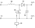
- FIG. 5 is a circuit diagram showing a circuit configuration example of the DC-DC converter.
- This DC-DC converter is a boost converter that outputs power having a voltage higher than an input voltage.
- This DC-DC converter includes an inductor 30, a diode 31, a switch element 32, a capacitor 33, and a control circuit 35.
- the switch element 32 is configured by, for example, a MOS (Metal-Oxide-Semiconductor) transistor.
- the MOS transistor is in a state in which a current flows between the source (S) and the drain (D) in accordance with a switching control signal (digital pulse signal composed of logical values 0 and 1) applied to the gate (G) (ON state) ) And a state in which no current flows (off state).
- the control circuit 35 has a function of generating a switching control signal to be supplied to the switch element 32.
- the control circuit 35 controls the duty ratio of the switching control signal by PWM (Pulse Width Modulation) control using the control signal (analog signal) applied from the control device 8 (signal adjustment devices 9 and 11). It has a function.
- the duty ratio is a ratio of pulse widths of logical values 1 and 0 in the switching control signal.
- the control circuit 35 is a circuit that controls the output power of the DC-DC converter.
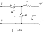
- FIG. 6 is a circuit diagram showing another circuit configuration example of the DC-DC converter.
- This DC-DC converter is a step-down converter that outputs power having a voltage lower than an input voltage.
- This DC-DC converter includes an inductor 30, a diode 31, a switch element 32, a capacitor 33, and a control circuit 35.
- the switch element 32 is configured by a MOS transistor. Similar to the control circuit 35 shown in FIG. 5, the control circuit 35 supplies the switch element 32 by PWM control using a control signal (analog signal) applied from the control device 8 (signal adjustment devices 9 and 11). A function of controlling the duty ratio of the switching control signal. That is, the control circuit 35 is a circuit that controls the output power of the DC-DC converter.
- Each of the converters 5 to 7 has a DC-DC converter circuit as described above. Note that the circuit configuration employed as the converters 5 to 7 is not limited to that shown in FIGS. 5 and 6, and circuits other than those shown in FIGS. It may be a configuration.
- the current sensor 12 shown in FIG. 4 is a sensor that detects the magnitude of the current input to the converter 6, and outputs a signal having a magnitude proportional to the input current.
- the current sensor 13 is a sensor that detects the magnitude of the current output from the converter 6 and outputs a signal having a magnitude proportional to the output current.
- the control device 8 is a device having a function as a maximum power point tracking control device. That is, the control device 8 generates a control signal (control signal applied to the control circuit 35 of the DC-DC converter) for controlling the converter 6 so that the power at the maximum power point can be taken out from the photoelectric conversion cell 3. It has a function.
- Various algorithms for generating the control signal have been proposed. For example, as one of such algorithms, there is a P & O (Perturb) and Observe) method. In this P & O method, for example, the control device 8 increases or decreases the value of the control signal (analog signal) output to the control circuit 35 of the converter 6.
- the control device 8 detects the input voltage Vi input from the photoelectric conversion cell 3 to the converter 6, the output voltage Vo output from the converter 6, and the signal Ii output from the current sensor 12, and sets the detected value. Multiply the current and voltage based. Thereby, the control apparatus 8 calculates (estimates) the output power output from the photoelectric conversion cell 3, and monitors (monitors) the calculated output power. Thereby, when the control device 8 detects that the output power has changed in the increasing direction, the control device 8 further changes the value of the control signal in the same increasing direction or decreasing direction as described above. On the other hand, when the control device 8 detects that the output power has changed in the decreasing direction, the control device 8 changes the value of the control signal in the decreasing direction or the increasing direction, which is the opposite direction.
- the control device 8 keeps tracking the maximum power point so that the output power of the photoelectric conversion cell 3 becomes the maximum power point.
- the control device 8 corresponds to the algorithm adopted among the input voltage Vi input to the converter 6, the output voltage Vo output from the converter 6, and the signals Ii and Io output from the current sensors 12 and 13. Use voltage or signal.
- the signal (analog signal) generated by the control device 8 is a basic signal that is the basis of a plurality of control signals that respectively control the converters 5-7. That is, in the second embodiment, the signal (basic signal) generated by the control device 8 is directly applied to the control circuit 35 of the converter 6 as a control signal. Further, the signal is applied to the control circuit 35 of the converter 5 through the signal adjustment device 9. Further, the signal is applied to the control circuit 35 of the converter 7 via the signal adjustment device 11.
- the signal conditioners 9 and 11 have a circuit configuration (multiplier) for multiplying the basic signal output from the control device 8 by a constant.
- the constant by which the signal adjustment device 9 multiplies the basic signal is a numerical value corresponding to the ratio between the characteristic value of the photoelectric conversion cell 3 and the characteristic value of the photoelectric conversion cell 2.
- the constant that the signal adjustment device 11 multiplies the basic signal is a numerical value based on the ratio between the characteristic value of the photoelectric conversion cell 3 and the characteristic value of the photoelectric conversion cell 4. That is, the photoelectric conversion cells 2 to 4 have different sensitivity wavelength bands, and characteristic values such as an internal resistance value differ depending on the sensitivity wavelength band. Such characteristic values in the photoelectric conversion cells 2 to 4 are obtained in advance.
- the maximum power point of the photoelectric conversion cells 2 to 4 varies depending on the sunshine state of the photoelectric conversion cells 2 to 4, the ambient temperature, the load fluctuation on the output side connected to the photoelectric conversion cells 2 to 4, and the like.
- the ratio of the optimum operating voltage at which each of the photoelectric conversion cells 2 to 4 outputs the power at the maximum power point can be regarded as almost the same even if the maximum power point varies.
- the output device 14B has the maximum power point of the photoelectric conversion cells 2 and 4 by the control signal calculated by multiplying the basic signal by the control device 8 by a constant corresponding to the ratio of the characteristic values. Can follow.
- the output device 14B uses the control signal (basic signal) for controlling the converter 6 and uses not only the photoelectric conversion cell 3 but also the maximum power points of the photoelectric conversion cells 2 and 4. Can follow.
- the converter 6, the control device 8, the signal adjustment devices 9 and 11, and the current sensors 12 and 13 constitute a power converter 38.
- the output device 14B according to the second embodiment and the solar power generation device including the output device 14B are configured so that all the converters 2 to This is a configuration that does not need to be provided every four. Therefore, the solar power generation device according to the second embodiment is similar to the solar power generation device according to the first embodiment in that the control device 8 is compared with the case where the same number of control devices 8 are installed as the converters 5 to 7. 8 can be reduced, so that the cost can be reduced. Further, the output device 14B and the solar power generation device including the output device 14B can be simplified in configuration.
- control device 8 detects not only the photoelectric conversion cell 3 but also currents and voltages output from the photoelectric conversion cells 2 and 4, and outputs the plurality (all) of the photoelectric conversion cells 2 to 4. Monitor power. Then, the control device 8 generates a control signal (basic signal) for controlling the converter 6 so that the total value or average value of the plurality (all) of output powers becomes maximum.
- the configuration other than the part related to the control device 8 is the same as that of the second embodiment, and the description thereof is omitted here.
- the output device 14B according to the third embodiment and the solar power generation device including the output device 14B can obtain the same effects as those of the second embodiment.
- the control device 8 generates a control signal (basic signal) by using a total value or an average value of output powers of a plurality (all) of the photoelectric conversion cells 2 to 4. .
- the output device 14B of 3rd Embodiment and a solar power generation device provided with the same can output more electric power as the photoelectric part 21 whole.
- the signal conditioning devices 9 and 11 are integrated together with the converter 6 and the control device 8 as the same device to constitute the power converter 38.
- the signal adjustment device 9 is integrated as the same device 40 together with the converter 5.
- the signal conditioning device 11 is integrated as the same device 41 together with the converter 7.
- FIG. 7 is a circuit diagram showing a simplified configuration of the output device 14B, and illustration of the condensing lens 20A and the photoelectric unit 21 is omitted.
- the configuration other than the above is the same as that of the second and third embodiments, and the description thereof is omitted here.
- the output device 14B according to the fourth embodiment and the solar power generation device including the output device 14B can also obtain the same effects as those of the second and third embodiments.
- the solar power generation device includes a plurality of photoelectric conversion units 42 as shown in FIG.
- Each photoelectric conversion unit 42 includes a condenser lens 20 ⁇ / b> A and a photoelectric unit 21.
- the photoelectric conversion cells 2 having the same sensitivity wavelength band, the photoelectric conversion cells 3 and the photoelectric conversion cells 4 in each photoelectric conversion unit 42 are electrically connected in series or in parallel, respectively.
- FIG. 8 shows a state in which photoelectric conversion cells having the same sensitivity wavelength band are connected in series.
- the photoelectric conversion cells 2 having the same sensitivity wavelength band, the photoelectric conversion cells 3, and the photoelectric conversion cells 4 are electrically connected, and the corresponding common converter 5, converter 6, or converter 7. Connected to. That is, a plurality of photoelectric conversion cells 2 suitable for short wavelength band light are connected to a common converter 5. A plurality of photoelectric conversion cells 3 suitable for medium wavelength band light are connected to a common converter 6. A plurality of photoelectric conversion cells 4 suitable for the long wavelength band light are connected to a common converter 7.
- control device 8 that generates a basic signal that is a basis of control signals for controlling the converters 5 to 7, respectively.
- signal adjustment devices 9 and 11 for generating control signals suitable for the converters 5 and 7 which are signal supply partners by multiplying the basic signal by a constant.
- the output device of the fifth embodiment and the solar power generation device including the same are the second to fourth embodiments.
- the effect similar to the output device of each embodiment and a solar power generation device provided with the same can be acquired.
- the solar power generation apparatus has a configuration in which a constant multiplied by the basic signal by the signal adjustment devices 9 and 11 is changed according to a predetermined condition. That is, the ratio of the characteristic values of the photoelectric conversion cells 2 to 4 changes slowly due to slow fluctuations in the conditions (environment) caused by the sun's diurnal and annual movements.
- a slow change in the ratio of the characteristic values of the photoelectric conversion cells 2 to 4 is taken into consideration. That is, the control device 8 changes (updates) the constant that the signal adjustment devices 9 and 11 multiply the basic signal according to the slow change in the characteristic value ratio of the photoelectric conversion cells 2 to 4 as described above.
- a function of outputting a command to the signal adjusting devices 9 and 11 is provided.
- the signal conditioners 9 and 11 change (update) constants to be multiplied by the basic signal according to the command.
- the output device of the sixth embodiment and the solar power generation device including the same can also obtain the same effects as those of the second to fifth embodiments.
- control device 8 constitutes a power converter 38 together with the converter 6.
- control device 8 may constitute a power converter together with the converter 5 or the converter 7.
- the control apparatus 8 is based on the information regarding the electric power input and output to the converter 6, such as the input voltage and input current which are input into the converter 6, and the output voltage and output current which are output from the converter 6.
- the basic signal is generated.
- the control device 8 may generate a basic signal based on information about power input to and output from the converter 5 and the converter 7.
- the solar power generation apparatus has three types of photoelectric conversion cells 2 to 4 corresponding to the three wavelength bands, respectively.
- the solar power generation device only needs to have a plurality of types of photoelectric conversion cells respectively corresponding to two or more types of wavelength bands, and two types of photoelectric conversion cells respectively corresponding to two types of wavelength bands. Or four or more types of photoelectric conversion cells respectively corresponding to four or more types of wavelength bands.
- the plurality of types of photoelectric conversion cells have the form shown in FIG. 3, but the form of the photoelectric conversion cell is not limited to the form of FIG.
- the present invention relates to solar power generation technology and can be used in various fields related to energy.
Landscapes
- Engineering & Computer Science (AREA)
- Power Engineering (AREA)
- Photovoltaic Devices (AREA)
- Control Of Electrical Variables (AREA)
Abstract
Description
本発明の出力装置は、
互いに異なる感度波長帯を持つ複数種の光電変換セルのうちの各々に接続し、接続している前記光電変換セルから出力する電力の変換機能を有する複数のコンバータと、
前記複数種の光電変換セルのうちの少なくとも一種から出力する出力電力に基づいて、前記出力電力の出力元である前記光電変換セルから出力される電力が最大電力点となるように前記複数のコンバータをそれぞれ制御する複数の制御信号の基となる基礎信号を生成する制御装置と、
前記基礎信号を定数倍し、定数倍した信号を前記制御信号として信号供給相手である前記コンバータに供給する信号調整装置とを備える。
互いに異なる感度波長帯を持つ複数種の光電変換セルと、
上記本発明の出力装置とを備える。
互いに異なる感度波長帯を持つ複数種の光電変換セルのうちの少なくとも一種から出力する出力電力に基づいて、前記出力電力の出力元である前記光電変換セルから出力される電力が最大電力点となるように、前記複数種の光電変換セルにそれぞれ接続されている複数のコンバータをそれぞれ制御する複数の制御信号の基となる基礎信号を生成し、
前記基礎信号を定数倍し、定数倍した信号を前記制御信号として信号供給相手である前記コンバータに供給し、
前記コンバータが、前記制御信号に基づいて動作することによって、前記光電変換セルから出力された電力を変換して出力する。
図1は、本発明に係る第1実施形態の出力装置およびそれを備えた太陽光発電装置の構成を簡略化して表すモデル図である。この第1実施形態の太陽光発電装置は、複数種の光電変換セル2,3,4と、出力装置14Aとを有している。
以下に、本発明に係る第2実施形態を説明する。
以下に、本発明に係る第3実施形態を説明する。なお、この第3実施形態の説明において、第2実施形態の太陽光発電装置における構成部分と同一の名称部分には同一符号を付し、その共通部分の重複説明は省略する。
以下に、本発明に係る第4実施形態を説明する。なお、この第4実施形態の説明において、第2や第3の実施形態の太陽光発電装置を構成する構成部分と同一の名称部分には同一符号を付し、その共通部分の重複説明は省略する。
以下に、本発明に係る第5実施形態を説明する。なお、この第5実施形態の説明において、第2~第4の実施形態の太陽光発電装置を構成する構成部分と同一の名称部分には同一符号を付し、その共通部分の重複説明は省略する。
以下に、本発明に係る第6実施形態を説明する。なお、この第6実施形態の説明において、第2~第5の実施形態の太陽光発電装置と同一の名称部分には同一符号を付し、その共通部分の重複説明は省略する。
本発明は第1~第6の各実施形態の構成に限定されず、様々な実施の形態を採り得る。例えば、第2~第6の各実施形態では、制御装置8は、コンバータ6と共に、パワーコンバータ38を構成している。これに代えて、制御装置8は、コンバータ5あるいはコンバータ7と共に、パワーコンバータを構成してもよい。
5,6,7, コンバータ
8 制御装置
9,10,11 信号調整装置
14A,14B,14D 出力装置
20A,20B 集光レンズ
Claims (10)
- 互いに異なる感度波長帯を持つ複数種の光電変換セルのうちの各々に接続し、接続している前記光電変換セルから出力する電力の変換機能を有する複数のコンバータと、
前記複数種の光電変換セルのうちの少なくとも一種から出力する出力電力に基づいて、前記出力電力の出力元である前記光電変換セルから出力される電力が最大電力点となるように前記複数のコンバータをそれぞれ制御する複数の制御信号の基となる基礎信号を生成する制御装置と、
前記基礎信号を定数倍し、定数倍した信号を前記制御信号として信号供給相手である前記コンバータに供給する信号調整装置とを備える出力装置。 - 前記制御装置は、前記複数種の光電変換セルから出力された電力の合計値又は平均値が最大となるように前記基礎信号を生成する請求項1記載の出力装置。
- 前記信号調整装置が前記基礎信号に乗算する定数は、前記制御装置が前記基礎信号を生成する場合に利用する電力の出力元の前記光電変換セルの特性値と、前記信号調整装置が前記制御信号を出力する出力先の前記コンバータが接続している前記光電変換セルの特性値との比に基づいて定められている請求項1又は請求項2記載の出力装置。
- 前記信号調整装置は、前記基礎信号に乗算する定数を予め定められた条件に応じて変更する請求項1又は請求項2又は請求項3記載の出力装置。
- 前記信号調整装置は、前記制御信号の変動よりも遅い変動に対応して、前記基礎信号に乗算する定数を変更する請求項4記載の出力装置。
- 前記制御装置は、前記コンバータの一つと共に、同じ装置として集約されている請求項1乃至請求項5の何れか一つに記載の出力装置。
- 前記信号調整装置は、前記信号供給相手である前記コンバータと共に、同じ装置として集約されている請求項1乃至請求項6の何れか一つに記載の出力装置。
- 互いに異なる感度波長帯を持つ複数種の光電変換セルと、
請求項1乃至請求項7の何れか一つに記載の出力装置とを備える太陽光発電装置。 - 光軸の周囲に色収差によってスペクトル分離したリング状の焦点を形成する集光レンズをさらに備え、
前記各種光電変換セルは、自身の感度波長帯に応じた前記焦点位置に配置されている請求項8記載の太陽光発電装置。 - 互いに異なる感度波長帯を持つ複数種の光電変換セルのうちの少なくとも一種から出力する出力電力に基づいて、前記出力電力の出力元である前記光電変換セルから出力される電力が最大電力点となるように、前記複数種の光電変換セルにそれぞれ接続されている複数のコンバータをそれぞれ制御する複数の制御信号の基となる基礎信号を生成し、
前記基礎信号を定数倍し、定数倍した信号を前記制御信号として信号供給相手である前記コンバータに供給し、
前記コンバータが、前記制御信号に基づいて動作することによって、前記光電変換セルから出力された電力を変換して出力する太陽光発電出力方法。
Priority Applications (2)
| Application Number | Priority Date | Filing Date | Title |
|---|---|---|---|
| US14/432,980 US20150244312A1 (en) | 2012-10-03 | 2013-10-01 | Power converter, solar energy device and solar energy power conversion method |
| JP2014539609A JPWO2014054271A1 (ja) | 2012-10-03 | 2013-10-01 | 出力装置、太陽光発電装置および太陽光発電出力方法 |
Applications Claiming Priority (2)
| Application Number | Priority Date | Filing Date | Title |
|---|---|---|---|
| JP2012220999 | 2012-10-03 | ||
| JP2012-220999 | 2012-10-03 |
Publications (1)
| Publication Number | Publication Date |
|---|---|
| WO2014054271A1 true WO2014054271A1 (ja) | 2014-04-10 |
Family
ID=50434615
Family Applications (1)
| Application Number | Title | Priority Date | Filing Date |
|---|---|---|---|
| PCT/JP2013/005841 Ceased WO2014054271A1 (ja) | 2012-10-03 | 2013-10-01 | 出力装置、太陽光発電装置および太陽光発電出力方法 |
Country Status (3)
| Country | Link |
|---|---|
| US (1) | US20150244312A1 (ja) |
| JP (1) | JPWO2014054271A1 (ja) |
| WO (1) | WO2014054271A1 (ja) |
Cited By (3)
| Publication number | Priority date | Publication date | Assignee | Title |
|---|---|---|---|---|
| US20160359066A1 (en) * | 2015-06-02 | 2016-12-08 | International Business Machines Corporation | ENERGY HARVESTING DEVICE with PREFABRICATED THIN FILM ENERGY ABSORPTION SHEETS AND ROLL-TO-SHEET AND ROLL-TO-ROLL FABRICATION THEREOF |
| US10290748B2 (en) | 2014-01-14 | 2019-05-14 | International Business Machines Corporation | Monolithically integrated thin-film device with a solar cell, an integrated battery, and a controller |
| US11004995B2 (en) | 2016-10-14 | 2021-05-11 | Kaneka Corporation | Photovoltaic device |
Families Citing this family (4)
| Publication number | Priority date | Publication date | Assignee | Title |
|---|---|---|---|---|
| JP6116741B1 (ja) * | 2016-08-14 | 2017-04-19 | 錬司 平瀬 | 光発電装置 |
| USD909975S1 (en) * | 2018-10-01 | 2021-02-09 | R&S Shaeffer Properties LLC | Wire harness connector |
| US20220302870A1 (en) * | 2021-03-19 | 2022-09-22 | Prathamesh Acharekar | Photovoltaic Module Array |
| USD962157S1 (en) * | 2021-03-19 | 2022-08-30 | Prathamesh Acharekar | Photovoltaic module |
Citations (4)
| Publication number | Priority date | Publication date | Assignee | Title |
|---|---|---|---|---|
| JP2004200326A (ja) * | 2002-12-17 | 2004-07-15 | Canon Inc | 電力変換装置 |
| WO2011074535A1 (ja) * | 2009-12-16 | 2011-06-23 | 日本電気株式会社 | 太陽光発電装置 |
| JP2011164964A (ja) * | 2010-02-10 | 2011-08-25 | Tabuchi Electric Co Ltd | 電力変換装置 |
| JP2012137830A (ja) * | 2010-12-24 | 2012-07-19 | Ntt Facilities Inc | 太陽光発電システム |
-
2013
- 2013-10-01 US US14/432,980 patent/US20150244312A1/en not_active Abandoned
- 2013-10-01 WO PCT/JP2013/005841 patent/WO2014054271A1/ja not_active Ceased
- 2013-10-01 JP JP2014539609A patent/JPWO2014054271A1/ja active Pending
Patent Citations (4)
| Publication number | Priority date | Publication date | Assignee | Title |
|---|---|---|---|---|
| JP2004200326A (ja) * | 2002-12-17 | 2004-07-15 | Canon Inc | 電力変換装置 |
| WO2011074535A1 (ja) * | 2009-12-16 | 2011-06-23 | 日本電気株式会社 | 太陽光発電装置 |
| JP2011164964A (ja) * | 2010-02-10 | 2011-08-25 | Tabuchi Electric Co Ltd | 電力変換装置 |
| JP2012137830A (ja) * | 2010-12-24 | 2012-07-19 | Ntt Facilities Inc | 太陽光発電システム |
Cited By (4)
| Publication number | Priority date | Publication date | Assignee | Title |
|---|---|---|---|---|
| US10290748B2 (en) | 2014-01-14 | 2019-05-14 | International Business Machines Corporation | Monolithically integrated thin-film device with a solar cell, an integrated battery, and a controller |
| US10559702B2 (en) | 2014-01-14 | 2020-02-11 | International Business Machines Corporation | Monolithically integrated thin-film device with a solar cell, an integrated battery, and a controller |
| US20160359066A1 (en) * | 2015-06-02 | 2016-12-08 | International Business Machines Corporation | ENERGY HARVESTING DEVICE with PREFABRICATED THIN FILM ENERGY ABSORPTION SHEETS AND ROLL-TO-SHEET AND ROLL-TO-ROLL FABRICATION THEREOF |
| US11004995B2 (en) | 2016-10-14 | 2021-05-11 | Kaneka Corporation | Photovoltaic device |
Also Published As
| Publication number | Publication date |
|---|---|
| US20150244312A1 (en) | 2015-08-27 |
| JPWO2014054271A1 (ja) | 2016-08-25 |
Similar Documents
| Publication | Publication Date | Title |
|---|---|---|
| WO2014054271A1 (ja) | 出力装置、太陽光発電装置および太陽光発電出力方法 | |
| Jotham Jeremy et al. | Non-isolated conventional DC-DC converter comparison for a photovoltaic system: A review | |
| Sivakumar et al. | An assessment on performance of DC–DC converters for renewable energy applications | |
| Saravanan et al. | A modified high step-up non-isolated DC-DC converter for PV application | |
| JP5276349B2 (ja) | 光起電性電源から電力を取り出すためのシステム、方法及び装置 | |
| US9136710B1 (en) | Multi-path converters for PV substrings | |
| JP6337280B2 (ja) | コンバータと多段倍電圧整流回路を併用した、部分影補償機能を付加した統合型太陽電池用コンバータ | |
| KR20150023888A (ko) | 태양 전지 설비를 위한 국부화된 파워 포인트 옵티마이저 | |
| JPH11103538A (ja) | 光発電システム | |
| US20130099760A1 (en) | Direct-current stabilized power supply device | |
| JP5807283B2 (ja) | 直列接続された蓄電セルの中間タップとバランス回路とdc−dcコンバータを併用した電力変換装置 | |
| US20120101645A1 (en) | Power control method using orthogonal-perturbation, power generation system, and power converter | |
| JP2024513793A (ja) | マルチレベル構造を有する電力変換装置 | |
| JP6511686B2 (ja) | コンバータ、太陽電池モジュール用コンバータシステム、及び蓄電モジュール用コンバータシステム | |
| KR20120013199A (ko) | 파셜 파워 마이크로-컨버터 아키텍처 | |
| Singh et al. | SEPIC converter for solar PV array fed battery charging in DC homes | |
| JP6307334B2 (ja) | 太陽電池制御装置 | |
| KR20150073680A (ko) | 최대 전력 추종 장치 및 방법 | |
| US20140375132A1 (en) | Smart photovoltaic modules with high dc-ac ratios | |
| KR20230006275A (ko) | 멀티레벨 구조를 가지는 전력변환장치 | |
| JP2015076528A (ja) | 昇降圧コンバータを多段接続した太陽電池部分影補償装置 | |
| KR20210109795A (ko) | 신재생 에너지와 에너지 저장장치를 위한 전력계통 연계형 통합 컨버터 | |
| KR101779055B1 (ko) | 집광형 태양전지모듈을 위한 스트링 전력컨버터시스템 | |
| Samaddar et al. | Series Balancing Capacitor (SBC) based DMPPT Scheme for string of PV Modules operating under non-uniform operating conditions | |
| JP2024513787A (ja) | マルチレベル構造を有する電力変換装置 |
Legal Events
| Date | Code | Title | Description |
|---|---|---|---|
| 121 | Ep: the epo has been informed by wipo that ep was designated in this application |
Ref document number: 13843283 Country of ref document: EP Kind code of ref document: A1 |
|
| ENP | Entry into the national phase |
Ref document number: 2014539609 Country of ref document: JP Kind code of ref document: A |
|
| WWE | Wipo information: entry into national phase |
Ref document number: 14432980 Country of ref document: US |
|
| NENP | Non-entry into the national phase |
Ref country code: DE |
|
| 122 | Ep: pct application non-entry in european phase |
Ref document number: 13843283 Country of ref document: EP Kind code of ref document: A1 |