WO2014049972A1 - 太陽電池モジュールの製造方法、太陽電池セルの製造方法及び太陽電池モジュールの製造システム - Google Patents
太陽電池モジュールの製造方法、太陽電池セルの製造方法及び太陽電池モジュールの製造システム Download PDFInfo
- Publication number
- WO2014049972A1 WO2014049972A1 PCT/JP2013/005214 JP2013005214W WO2014049972A1 WO 2014049972 A1 WO2014049972 A1 WO 2014049972A1 JP 2013005214 W JP2013005214 W JP 2013005214W WO 2014049972 A1 WO2014049972 A1 WO 2014049972A1
- Authority
- WO
- WIPO (PCT)
- Prior art keywords
- solar cells
- solar
- manufacturing
- solar cell
- cell module
- Prior art date
- Legal status (The legal status is an assumption and is not a legal conclusion. Google has not performed a legal analysis and makes no representation as to the accuracy of the status listed.)
- Ceased
Links
Images


Classifications
-
- H—ELECTRICITY
- H10—SEMICONDUCTOR DEVICES; ELECTRIC SOLID-STATE DEVICES NOT OTHERWISE PROVIDED FOR
- H10F—INORGANIC SEMICONDUCTOR DEVICES SENSITIVE TO INFRARED RADIATION, LIGHT, ELECTROMAGNETIC RADIATION OF SHORTER WAVELENGTH OR CORPUSCULAR RADIATION
- H10F71/00—Manufacture or treatment of devices covered by this subclass
- H10F71/137—Batch treatment of the devices
-
- H—ELECTRICITY
- H02—GENERATION; CONVERSION OR DISTRIBUTION OF ELECTRIC POWER
- H02S—GENERATION OF ELECTRIC POWER BY CONVERSION OF INFRARED RADIATION, VISIBLE LIGHT OR ULTRAVIOLET LIGHT, e.g. USING PHOTOVOLTAIC [PV] MODULES
- H02S50/00—Monitoring or testing of PV systems, e.g. load balancing or fault identification
- H02S50/10—Testing of PV devices, e.g. of PV modules or single PV cells
-
- H—ELECTRICITY
- H10—SEMICONDUCTOR DEVICES; ELECTRIC SOLID-STATE DEVICES NOT OTHERWISE PROVIDED FOR
- H10F—INORGANIC SEMICONDUCTOR DEVICES SENSITIVE TO INFRARED RADIATION, LIGHT, ELECTROMAGNETIC RADIATION OF SHORTER WAVELENGTH OR CORPUSCULAR RADIATION
- H10F19/00—Integrated devices, or assemblies of multiple devices, comprising at least one photovoltaic cell covered by group H10F10/00, e.g. photovoltaic modules
- H10F19/90—Structures for connecting between photovoltaic cells, e.g. interconnections or insulating spacers
- H10F19/902—Structures for connecting between photovoltaic cells, e.g. interconnections or insulating spacers for series or parallel connection of photovoltaic cells
-
- Y—GENERAL TAGGING OF NEW TECHNOLOGICAL DEVELOPMENTS; GENERAL TAGGING OF CROSS-SECTIONAL TECHNOLOGIES SPANNING OVER SEVERAL SECTIONS OF THE IPC; TECHNICAL SUBJECTS COVERED BY FORMER USPC CROSS-REFERENCE ART COLLECTIONS [XRACs] AND DIGESTS
- Y02—TECHNOLOGIES OR APPLICATIONS FOR MITIGATION OR ADAPTATION AGAINST CLIMATE CHANGE
- Y02E—REDUCTION OF GREENHOUSE GAS [GHG] EMISSIONS, RELATED TO ENERGY GENERATION, TRANSMISSION OR DISTRIBUTION
- Y02E10/00—Energy generation through renewable energy sources
- Y02E10/50—Photovoltaic [PV] energy
-
- Y—GENERAL TAGGING OF NEW TECHNOLOGICAL DEVELOPMENTS; GENERAL TAGGING OF CROSS-SECTIONAL TECHNOLOGIES SPANNING OVER SEVERAL SECTIONS OF THE IPC; TECHNICAL SUBJECTS COVERED BY FORMER USPC CROSS-REFERENCE ART COLLECTIONS [XRACs] AND DIGESTS
- Y02—TECHNOLOGIES OR APPLICATIONS FOR MITIGATION OR ADAPTATION AGAINST CLIMATE CHANGE
- Y02P—CLIMATE CHANGE MITIGATION TECHNOLOGIES IN THE PRODUCTION OR PROCESSING OF GOODS
- Y02P70/00—Climate change mitigation technologies in the production process for final industrial or consumer products
- Y02P70/50—Manufacturing or production processes characterised by the final manufactured product
Definitions
- the present invention relates to a solar cell module manufacturing method, a solar cell manufacturing method, and a solar cell module manufacturing system.
- the solar cell module includes a plurality of solar cells connected by a wiring material, and a protective member such as a glass substrate that protects the solar cells (for example, see Patent Document 1).
- the solar cells are ranked according to the output in the manufacturing process, and a plurality of solar cells constituting the solar cell module are selected from each rank according to the target output of the solar cell module. This selection is performed using the center value of the output width of each rank. That is, a plurality of solar cells are selected so that the solar cell module output calculated using the center value of each rank satisfies the target output.
- the output distribution of the manufactured solar battery cell fluctuates, when a solar battery cell is selected using the above-mentioned center value, there are cases where many solar battery modules that do not satisfy the target output are generated due to variations in module output. Therefore, in order to suppress the generation of solar battery modules that do not satisfy the target output, it is necessary to select solar cells so that the output is slightly higher than the target output. For this reason, the usage amount of the solar cells located on the high output side in the output distribution increases, the inventory of the solar cells located on the high output side in the output distribution decreases, and the low output in the output distribution. The problem that the inventory of the photovoltaic cell located in the side increases occurs. When the inventory of solar cells of a specific rank increases, the solar cells of that rank must be disposed of.
- the method for manufacturing a solar cell module prepares a plurality of solar cells, measures the characteristic values of the solar cells, assigns the solar cells to a plurality of ranks based on the measured characteristic values, and ranks them.
- An average value of characteristic values is calculated for each set of a predetermined number of divided solar cells, and a plurality of solar cells are selected from at least one of the sets based on the average value and the target module characteristic value.
- a string of battery cells is produced.
- a standard deviation of characteristic values is calculated for each set, and a plurality of solar cells are selected from at least one of the sets based on the average value, the standard deviation, and the target module characteristic value, and a string of solar cells is produced. Is preferred.
- the solar cell module manufacturing system measures the characteristic values of the solar cells, distributes the solar cells to a plurality of ranks based on the measured characteristic values, and calculates the average value of the characteristic values for each rank. Means for calculating, and means for selecting a plurality of solar cells from at least one of the ranks to produce a string of the solar cells based on the average value and the target module characteristic value.
- a target solar cell module can be efficiently manufactured.
- FIG. 1 is a plan view of the solar cell module 10 as seen from the light receiving surface side.
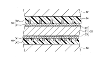
- FIG. 2 is a cross-sectional view of the solar cell module 10 cut in the thickness direction along line XX in FIG.
- the solar cell module 10 includes a plurality of solar cells 11, a first protective member 12 disposed on the light receiving surface side of the solar cell 11, and a second protective member 13 disposed on the back surface side of the solar cell 11. Is provided.
- the plurality of solar cells 11 are sandwiched between the first protective member 12 and the second protective member 13 and are sealed with a filler 14.
- a translucent member such as a glass substrate, a resin substrate, or a resin film can be used.
- the second protective member 13 for example, a white member that does not have translucency may be used.
- a resin such as ethylene vinyl acetate copolymer (EVA) can be used.
- the solar cell module 10 includes a wiring member 15 that connects a plurality of solar cells 11.
- the wiring member 15 bends in the thickness direction of the solar cell module 10 between the adjacent solar cells 11 and connects the solar cells 11 in series.
- the solar cell module 10 includes a transition wiring member 16 that connects the wiring members 15, a frame 17 that is attached to the periphery of the first protective member 12 and the second protective member 13, a terminal box (not shown), and the like.
- a string 18 in which a plurality of solar cells 11 are connected in series is formed by the wiring member 15 and the transition wiring member 16.
- the solar cell 11 includes a photoelectric conversion unit 20 that generates carriers by receiving sunlight, a first electrode 30 that is a light receiving surface electrode formed on the light receiving surface, and a back surface formed on the back surface. And a second electrode 40 that is an electrode.
- the carriers generated by the photoelectric conversion unit 20 are collected by the first electrode 30 and the second electrode 40, respectively.
- the “light receiving surface” means a surface on which sunlight mainly enters from the outside of the solar battery cell 11
- the “back surface” means a surface opposite to the light receiving surface. For example, more than 50% to 100% of the sunlight incident on the solar battery cell 11 is incident from the light receiving surface side.
- the photoelectric conversion unit 20 includes a substrate 21 made of a semiconductor material such as crystalline silicon (c-Si), gallium arsenide (GaAs), indium phosphide (InP), and an amorphous semiconductor formed on the light receiving surface of the substrate 21.
- a layer 22 and an amorphous semiconductor layer 23 formed on the back surface of the substrate 21 are included.
- As the substrate 21, an n-type single crystal silicon substrate is particularly suitable.
- the amorphous semiconductor layer 22 has a layer structure in which, for example, an i-type amorphous silicon layer and a p-type amorphous silicon layer are sequentially formed.
- the amorphous semiconductor layer 23 has a layer structure in which, for example, an i-type amorphous silicon layer and an n-type amorphous silicon layer are sequentially formed.
- the first electrode 30 has a transparent conductive layer 31 formed on the amorphous semiconductor layer 22 and a collector electrode 32 formed on the transparent conductive layer 31.
- the second electrode 40 includes a transparent conductive layer 41 and a collecting electrode 42.
- the collector electrode 42 has a larger area than the collector electrode 32.
- the transparent conductive layers 31 and 41 are made of, for example, a transparent conductive oxide obtained by doping metal oxide such as indium oxide (In 2 O 3 ) or zinc oxide (ZnO) with tin (Sn), antimony (Sb), or the like. Composed.
- the collector electrodes 32 and 42 have a structure in which conductive fillers are dispersed in a binder resin such as an epoxy resin, for example.
- a binder resin such as an epoxy resin, for example.
- the conductive filler metal particles such as silver (Ag), copper (Cu), nickel (Ni), carbon, or a mixture thereof can be used. Of these, Ag particles are preferred.
- the collector electrodes 32 and 42 may be metal plating electrodes formed by Ag or Cu plating.
- the collecting electrodes 32 and 42 are preferably composed of a plurality of finger portions and a plurality of (for example, two or three) bus bar portions.
- the finger part is a thin line-like electrode formed over a wide range on the transparent conductive layers 31 and 41, and the bus bar part is an electrode that collects carriers from the finger electrode.
- the collector electrode 42 may be comprised from metal layers, such as Ag, instead of a finger part.
- a structure other than the above can be applied to the photoelectric conversion unit.
- an i-type amorphous silicon layer and an n-type amorphous silicon layer are sequentially formed on the light-receiving surface side of a substrate made of n-type single crystal silicon or the like, and an i-type amorphous silicon layer is formed on the back surface side of the substrate.
- a photoelectric conversion part in which a p-type region composed of a p-type amorphous silicon layer and an n-type region composed of an i-type amorphous silicon layer and an n-type amorphous silicon layer are formed.
- electrodes p-side electrode and n-side electrode
- a photoelectric conversion unit including a substrate made of p-type polycrystalline silicon, an n-type diffusion layer formed on the light-receiving surface of the substrate, and an aluminum metal layer formed on the back surface of the substrate; Also good.
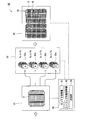
- FIG. 3 is a diagram illustrating a manufacturing process of the solar cell module manufacturing system 50 and the solar cell module 10.
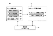
- FIG. 4 is a diagram illustrating a configuration of the control device 60.
- FIG. 5 is a flowchart showing the manufacturing procedure of the solar cell module 10.
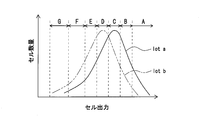
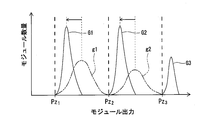
- FIG. 6 is a diagram showing the output distribution of the solar battery cells 11.
- FIG. 7 is a diagram showing the output distribution of the solar cell module 10.
- the solar cell module 10 can be manufactured using a manufacturing system 50.
- the characteristic value of the solar battery cell 11 is measured, and the solar battery cells 11 are assigned to a plurality of ranks based on the measured characteristic value.
- the process described here (hereinafter, “this process”
- the maximum output Pmax (Maximum Power) is used as the characteristic value.
- the solar cells 11 manufactured by a manufacturing facility (not shown) are transported to the selector device 51, the Pmax of the solar cells 11 is measured by the selector device 51, and a plurality of the solar cells 11 are based on Pmax. Sorted into ranks.
- the manufacturing system 50 includes the selector device 51 and a string manufacturing device 52 that connects the plurality of solar cells 11 with the wiring member 15 to form the string 18. Further, the manufacturing system 50 includes a cassette 53 that temporarily accommodates the solar cells 11 ranked by the selector device 51. In this step, seven ranks A, B, C, D, E, F, and G (see FIG. 6) are set in order from the highest Pmax. For ranks A to G, an upper limit value and a lower limit value for Pmax are defined, and for rank A, only a lower limit value for Pmax is defined. Solar cells 11 that are below the lower limit value of rank G are discarded as defective products, for example.
- the cassette 53 has at least seven cassettes 53 A to 53 G corresponding to the rank (in FIG.
- 53 E , 53 F and 53 G are omitted from the viewpoint of clarifying the drawing), and the cassettes 53 A to 53 G
- Each of 53 G can hold a predetermined number, for example, 100 solar cells 11.
- Each rank can be provided with a plurality of cassettes.
- the manufacturing system 50 includes a control device 60 that integrally controls the operation of the system.
- the control device 60 includes a selector control unit 61 that controls the selector device 51, a string production control unit 62 that controls the string production device 52, information for performing ranking of the solar cells 11, and a measured value of Pmax, which will be described later.
- Storage unit 63 for storing data such as average values and standard deviations. Examples of information for performing ranking include the upper limit value, the lower limit value, the target output of the solar cell module, and the like of each rank. In addition to these databases, the storage unit 63 can store arithmetic expressions such as standard deviations, control programs, and the like.
- FIG. 3 shows one control device 60 that controls the entire manufacturing system 50 in an integrated manner, but the functions of the control device 60 may be distributed among a plurality of hardware. Moreover, all the processes may be automatically performed by the function of the control device 60, or a part of this process may be manually performed.
- the selector control unit 61 and the string production control unit 62 of the control device 60 each include a plurality of control blocks.
- the selector control unit 61 includes a characteristic value measuring unit 64 that measures the Pmax of the solar battery cell 11, a rank determining unit 65 that distributes the solar battery cell 11 to each rank based on the measured Pmax, and an average value of Pmax for each rank.
- An average value calculating means 66 for calculating, and a standard deviation calculating means 67 for calculating a standard deviation of Pmax for each rank are included.
- the string production control unit 62 uses the average value and the standard deviation to calculate the module output calculation means 68 for calculating the minimum total Pmax of the plurality of solar cells 11, and the wiring material 15 to the selected plurality of solar cells 11. It includes string producing means 69 for attaching and producing the string 18.
- control apparatus 60 was set as the structure which calculates an average value and a standard deviation for every rank, you may comprise so that it may calculate for every manufacturing lot, and the predetermined number of photovoltaic cells 11 divided into each rank It is good also as a structure calculated for every group.
- the above set may be a unit composed of the maximum number of solar cells 11 that can be accommodated in the cassette, or may be a smaller unit, for example, a predetermined number unit smaller than the maximum number that can be accommodated in the cassette.
- the photoelectric conversion unit 20 is manufactured (S10). Specifically, an amorphous semiconductor layer 22 including an i-type amorphous silicon layer and a p-type amorphous silicon layer is formed on the light-receiving surface of the substrate 21, and an i-type amorphous film is formed on the back surface of the substrate 21.
- the photoelectric conversion part 20 is manufactured by forming the amorphous semiconductor layer 23 including the silicon layer and the n-type amorphous silicon layer.
- the amorphous semiconductor layers 22 and 23 are formed by, for example, CVD or sputtering by placing the cleaned substrate 21 in a vacuum chamber.
- a source gas obtained by diluting silane (SiH 4 ) with hydrogen (H 2 ) is used for forming the i-type amorphous silicon layer by CVD.
- a source gas diluted with hydrogen (H 2 ) by adding diborane (B 2 H 6 ) to silane can be used.
- a source gas diluted with hydrogen (H 2 ) by adding phosphine (PH 3 ) to silane can be used.
- the first electrode 30 and the second electrode 40 are formed on the photoelectric conversion unit 20 manufactured in S10 (S11).
- Transparent conductive layers 31 and 41 are first formed on the amorphous semiconductor layers 22 and 23 of the photoelectric conversion unit 20 by CVD or the like, respectively.
- collector electrodes 32 and 42 are formed on the transparent conductive layers 31 and 41 by screen printing or electrolytic plating, respectively.
- the solar battery cell 11 is manufactured by this process.
- the solar cell 11 In the manufacturing process of the solar cell 11, the solar cell 11 is manufactured under a certain manufacturing condition.
- Pmax varies due to fluctuations in conditions such as the amount of gas remaining in the vacuum chamber and the plasma generation state. To do.
- the variation in Pmax occurs.
- the peak position of the output distribution of Pmax also varies. For example, as shown in FIG. 6, the output distribution of the production lot a has a peak top in the range of rank B, but the output distribution of the production lot b has a peak top in the range of rank C.
- the plurality of solar cells 11 manufactured in S11 are conveyed to the selector device 51, assigned to ranks A to G, and accommodated in cassettes 53 A to 53 G corresponding to the ranks (S12 to S15). Steps S12 to S15 are automatically executed by the function of the selector control unit 61.
- Pmax is measured as a characteristic value of the plurality of solar battery cells 11.
- the open circuit voltage Voc, the short circuit current Isc, the fill factor FF, and the like may be included as the measured characteristic values.
- This step is automatically executed by the function of the characteristic value measuring means 64 of the selector control unit 61.
- Pmax is measured for all the solar cells 11. Pmax can be measured, for example, according to JIS C 8913.
- the solar cells 11 are assigned to a plurality of ranks A to G based on Pmax measured in S12 (S13).
- This step is executed by the function of the rank determination means 65. Specifically, an upper limit value and a lower limit value of Pmax defining each rank A to G stored in advance in the storage unit 63 are compared with the Pmax of the solar battery cell 11 measured in S12, and the solar battery The cell 11 is classified into ranks A to G.
- the solar cells 11 classified into ranks A to G are transported to the cassettes 53 A to 53 G by transport means (not shown).
- the measured value K of Pmax is also arranged for each rank and stored in the storage unit 63.
- the order stored in the cassettes 53 A to 53 G of the solar battery cell 11 and the measured value of Pmax are preferable. More preferably, K is stored as a set of data.
- average values X A to X G are calculated for each rank with respect to Pmax of the plurality of solar cells 11 ranked in S13 (S14).
- This step is executed by the function of the average value calculation means 66.
- the average values X A to X of Pmax for each rank are obtained by adding together the measured values K arranged for each rank and dividing by the number of measured values K (hereinafter referred to as “number of data N”). G is calculated.
- the calculation of the average values X A to X G may be executed sequentially every time Pmax is measured, or may be executed after all Pmax measurements have been completed.
- the standard deviations ⁇ A to ⁇ G of Pmax are calculated for each rank using the average values X A to X G calculated in S13 (S15). This step is executed by the function of the standard deviation calculating means 67.
- the standard deviations ⁇ A to ⁇ G are calculated for each rank based on each of the measurement value K arranged for each rank, the number of data N for each rank, and the average values X A to X G.
- the standard deviations ⁇ A to ⁇ G are calculated in accordance with, for example, the timing at which the average values X A to X G are calculated.
- the so-called 2 ⁇ and 3 ⁇ values that are twice or three times the standard deviations ⁇ A to ⁇ G in S13.
- the standard deviations ⁇ A to ⁇ G may be calculated in S13
- 2 ⁇ A to 2 ⁇ G and 3 ⁇ A to 3 ⁇ G may be calculated in S16 described later.
- the average values X A to X G and the standard deviations ⁇ A to ⁇ G are stored in the storage unit 63 in association with each other, for example.
- the stored average values X A to X G and standard deviations ⁇ A to ⁇ G are used as a database used when the string 18 is produced.
- the information of the average values X A to X G and the standard deviations ⁇ A to ⁇ G may be displayed on the corresponding cassette at the time when the process in the selector device 51 is completed.
- An example of such display is a method of printing characters and bar codes indicating the average value X and standard deviation ⁇ on a label and sticking the label to the cassettes 53 A to 53 G.
- Steps S16 and S17 are automatically executed by the function of the string production control unit 62.
- a plurality of solar cells from at least one of the cassettes 53 A to 53 G corresponding to the ranks A to G Cell 11 is selected.
- This step is executed by the function of the module output calculation means 68 of the string production control unit 62.
- the total Pmax of the plurality of solar cells 11 calculated from the average values X A to X G and the standard deviations ⁇ A to ⁇ G , that is, the predicted output of the solar cell module 10 is the target module output Pz.
- the solar battery cell 11 is selected so that it becomes the above.
- the combinations are not particularly limited. However, for selection of such solar cells 11, it is preferable that the number of stocks for each rank of the solar cells 11 in the cassettes 53 A to 53 G be one of the selection conditions.
- the target module output Pz may be the total Pmax of the selected plurality of solar cells 11, or for the selected plurality of solar cells 11, the solar cell module 10 after the laminating process described later. It may be Pmax of the state.
- the Pmax of the state of the solar cell module 10 is set as the target module output Pz, the correlation coefficient between the total Pmax of the selected plurality of solar cells 11 and the Pmax of the state of the solar cell module 10 is determined.
- the solar battery cell 11 may be selected. For example, when Pmax in the state of the solar cell module 10 is larger than the total Pmax of the selected plurality of solar cells 11, the output value is smaller than Pmax in the state of the solar cell module 10 in consideration of the correlation coefficient. A plurality of solar cells 11 are selected.
- the total Pmax is calculated by Equation 1.
- U, V, and W are the numbers of the solar cells 11 acquired from the cassettes 53 A , 53 B , and 53 C.
- the number of cassettes can be arbitrarily set.
- the calculated minimum value of total Pmax is equal to or greater than the target module output Pz, and the minimum value is It is preferable to select the solar battery cell 11 so as to have a value close to the target module output Pz. At this time, it is particularly preferable to calculate the total Pmax using values (2 ⁇ A to ⁇ G , 3 ⁇ A to ⁇ G ) that are twice or three times the standard deviations ⁇ A to ⁇ G.
- a plurality of grades of solar cell modules 10 having greatly different module outputs can be manufactured from the plurality of solar cells 11 accommodated in the cassettes 53 A to 53 G.
- two types of solar cell modules G1 and G2 having target module outputs Pz1 and Pz2 can be manufactured.
- FIG. 7 is a diagram showing the frequency distribution of the module output (Pmax), and the solar cells G1 and G2 manufactured in this process are selected by the solid line and the solar cells are selected using the center values of ranks A to G.
- the solar cell modules g1 and g2 (comparative examples) manufactured by doing so are indicated by two-dot chain lines.
- the module output can be predicted with high accuracy. For this reason, the peak of frequency distribution is sharp compared with the case of the solar cell modules g1 and g2, and the dispersion
- the peaks of the solar cell modules G1 and G2 are greatly shifted toward the target module outputs Pz1 and Pz2 than the peaks of the solar cell modules g1 and g2.
- the prediction accuracy of the module output is higher than in the case of the comparative example, it is possible to sufficiently prevent the generation of the solar cell module that does not satisfy the target output without giving a large margin to the module output.
- the solar cell module G1 it can manufacture using many photovoltaic cells located in the low output side in the output distribution which inventory tends to increase in a comparative example.
- the solar cell module G2 it can manufacture using the photovoltaic cell located in a high output in the output distribution which a stock tends to reduce in a comparative example.
- the wiring material 15 is connected to the plurality of solar cells 11 selected in S16 to produce the string 18 (S17). This process is automatically executed by the function of the string creating means 69.
- the wiring member 15 is attached to the collector electrodes 32 and 42 using, for example, an adhesive made of a film-like or paste-like thermosetting resin, and connects the plurality of solar battery cells 11 in series.
- the constituent members of the solar cell module 10 including the string 18 produced in S17 are stacked and thermocompression bonded (S18).
- This process is called a laminating process and is performed using a laminator (not shown).
- the filler 14 is supplied in the form of a film.
- the laminating step the first resin film constituting the filler 14 is laminated on the first protective member 12, and the string 18 is laminated on the first resin film.
- a second resin film constituting the filler 14 is laminated on the string 18, and the second protective member 13 is laminated thereon. And it laminates by applying a pressure from the 2nd protection member 13 side, heating at the temperature which each resin film melts.
- the frame 17 and the terminal box are attached, and the solar cell module 10 is manufactured.
- the solar cells 11 are assigned to each rank using Pmax as a characteristic value.
- the distribution may be executed using a characteristic value other than Pmax.
- characteristic values other than Pmax include the fill factor FF, sheet resistance R, short-circuit current Isc, open-circuit voltage Voc, and the like of the solar battery cell 11.
- the solar cells 11 are assigned to the respective ranks using only Pmax as a characteristic value, but a plurality of characteristic values may be used.
- the solar cells 11 that do not satisfy the predetermined short-circuit current Isc may be defective, and the other solar cells 11 may be assigned to each rank using Pmax as a characteristic value.
- the several photovoltaic cell 11 which comprises the solar cell module 10 was selected using the average value X and standard deviation (sigma) of the characteristic value in each rank, a photovoltaic cell was used using only the average value X. 11 may be selected.
- the target solar cell module 10 can be manufactured efficiently.
- the module output to be manufactured is accurately predicted by using the average value and the standard deviation of the solar cell output calculated for each rank in the selection of the solar cells 11 ranked. It becomes possible. For this reason, it becomes easy to obtain the target module output, and the dispersion
Landscapes
- Photovoltaic Devices (AREA)
Description
本発明は、太陽電池モジュールの製造方法、太陽電池セルの製造方法及び太陽電池モジュールの製造システムに関する。
太陽電池モジュールは、配線材により接続された複数の太陽電池セル、及び太陽電池セルを保護するガラス基板等の保護部材等を備える(例えば、特許文献1参照)。太陽電池セルは、例えば、製造過程において出力に応じてランク分けされ、太陽電池モジュールを構成する複数の太陽電池セルは、太陽電池モジュールの目標出力に応じて各ランクから選択される。この選択は、各ランクの出力幅の中心値を用いて行われる。即ち、各ランクの中心値を用いて算出した太陽電池モジュール出力が目標出力を満たすように複数の太陽電池セルが選択される。
しかし、製造される太陽電池セルの出力分布は変動するため、上記中心値を用いて太陽電池セルを選択すると、モジュール出力がばらついて目標出力を満たさない太陽電池モジュールが多く発生する場合がある。そこで、かかる目標出力を満たさない太陽電池モジュールの発生を抑制すべく、目標出力より少し高い出力となるように太陽電池セルを選択する必要がある。このため、出力分布の中で高出力側に位置する太陽電池セルの使用量が多くなり、出力分布の中で高出力側に位置する太陽電池セルの在庫が減り、出力分布の中で低出力側に位置する太陽電池セルの在庫が増えるという問題が発生する。特定のランクの太陽電池セルの在庫が増えると、そのランクの太陽電池セルを処分しなければならなくなる。
本発明に係る太陽電池モジュールの製造方法は、複数の太陽電池セルを準備し、太陽電池セルの特性値を測定し、測定した特性値に基づいて太陽電池セルを複数のランクに振り分け、ランクに分けられた所定数の太陽電池セルの組毎に特性値の平均値を算出し、平均値及び目標モジュール特性値に基づいて、組の少なくとも1つから複数の太陽電池セルを選択して該太陽電池セルのストリングを作製する。
組毎に特性値の標準偏差を算出し、平均値、標準偏差、及び目標モジュール特性値に基づいて、組の少なくとも1つから複数の太陽電池セルを選択して太陽電池セルのストリングを作製することが好適である。
本発明に係る太陽電池モジュールの製造システムは、太陽電池セルの特性値を測定し、測定した特性値に基づいて太陽電池セルを複数のランクに振り分ける手段と、ランク毎に特性値の平均値を算出する手段と、平均値及び目標モジュール特性値に基づいて、ランクの少なくとも1つから複数の太陽電池セルを選択して該太陽電池セルのストリングを作製する手段とを備える。
本発明によれば、目的とする太陽電池モジュールを効率良く製造することができる。
図面を参照しながら、本発明に係る実施形態の一例である太陽電池モジュール10の製造方法、及び太陽電池モジュールの製造システム50について以下詳細に説明するが、本発明の適用はこれに限定されない。
実施形態において参照する図面は、模式的に記載されたものであり、図面に描画された構成要素の寸法比率などは、現物と異なる場合がある。具体的な寸法比率等は、以下の説明を参酌して判断されるべきである。
実施形態において参照する図面は、模式的に記載されたものであり、図面に描画された構成要素の寸法比率などは、現物と異なる場合がある。具体的な寸法比率等は、以下の説明を参酌して判断されるべきである。
図1及び図2を参照して、太陽電池モジュール10の構成について説明する。図1は、太陽電池モジュール10を受光面側から見た平面図である。図2は、図1のX‐X線で太陽電池モジュール10を厚み方向に切断した断面図である。
太陽電池モジュール10は、複数の太陽電池セル11と、太陽電池セル11の受光面側に配置される第1保護部材12と、太陽電池セル11の裏面側に配置される第2保護部材13とを備える。複数の太陽電池セル11は、第1保護部材12と第2保護部材13とにより挟持されると共に、充填材14により封止されている。第1保護部材12及び第2保護部材13には、例えば、ガラス基板や樹脂基板、樹脂フィルム等の透光性を有する部材を用いることができる。第2保護部材13には、透光性を有さない、例えば白色の部材を用いてもよい。充填材14には、例えば、エチレン酢酸ビニル共重合体(EVA)等の樹脂を用いることができる。
太陽電池モジュール10は、複数の太陽電池セル11を接続する配線材15を備える。配線材15は、隣接する太陽電池セル11同士の間で太陽電池モジュール10の厚み方向に曲がり、各太陽電池セル11を直列に接続する。また、太陽電池モジュール10は、配線材15同士を接続する渡り配線材16、第1保護部材12及び第2保護部材13の周縁に取り付けられるフレーム17、図示しない端子ボックス等を備える。配線材15及び渡り配線材16により、複数の太陽電池セル11が直列に接続されたストリング18が形成されている。
太陽電池セル11は、太陽光を受光することでキャリアを生成する光電変換部20と、その受光面上に形成された受光面電極である第1電極30と、その裏面上に形成された裏面電極である第2電極40とをそれぞれ備える。太陽電池セル11では、光電変換部20で生成されたキャリアが、第1電極30及び第2電極40によりそれぞれ収集される。ここで、「受光面」とは太陽電池セル11の外部から太陽光が主に入射する面を、「裏面」とは受光面と反対側の面をそれぞれ意味する。例えば、太陽電池セル11に入射する太陽光のうち50%超過~100%が受光面側から入射する。
光電変換部20は、結晶系シリコン(c‐Si)、ガリウム砒素(GaAs)、インジウム燐(InP)等の半導体材料からなる基板21と、基板21の受光面上に形成された非晶質半導体層22と、基板21の裏面上に形成された非晶質半導体層23とを有する。基板21としては、n型単結晶シリコン基板が特に好適である。非晶質半導体層22は、例えば、i型非晶質シリコン層と、p型非晶質シリコン層とが順に形成された層構造である。非晶質半導体層23は、例えば、i型非晶質シリコン層と、n型非晶質シリコン層とが順に形成された層構造である。
第1電極30は、非晶質半導体層22上に形成された透明導電層31と、透明導電層31上に形成された集電極32とを有する。また、第2電極40は、第1電極30と同様に、透明導電層41と、集電極42とを有する。但し、集電極の面積は、集電極32よりも集電極42を大きくすることが好適である。
透明導電層31,41は、例えば、酸化インジウム(In2O3)や酸化亜鉛(ZnO)等の金属酸化物に、錫(Sn)やアンチモン(Sb)等をドープした透明導電性酸化物から構成される。集電極32,42は、例えば、エポキシ樹脂等のバインダ樹脂中に導電性フィラーが分散した構造を有する。導電性フィラーには、銀(Ag)、銅(Cu)、ニッケル(Ni)等の金属粒子やカーボン、又はこれらの混合物などを用いることができる。これらのうち、Ag粒子が好適である。或いは、集電極32,42は、AgやCuめっきにより形成される金属めっき電極であってもよい。
集電極32,42は、複数のフィンガー部、及び複数(例えば、2又は3本)のバスバー部からなることが好適である。フィンガー部は、透明導電層31,41上の広範囲に形成される細線状の電極であって、バスバー部は、フィンガー電極からキャリアを収集する電極である。なお、集電極42は、フィンガー部の代わりにAg等の金属層から構成されてもよい。
光電変換部には、上記以外の構造を適用することができる。例えば、n型単結晶シリコン等からなる基板の受光面側に、i型非晶質シリコン層及びn型非晶質シリコン層を順に形成し、基板の裏面側に、i型非晶質シリコン層及びp型非晶質シリコン層で構成されたp型領域と、i型非晶質シリコン層及びn型非晶質シリコン層で構成されたn型領域とを形成した光電変換部であってもよい。この場合、基板の裏面側のみに電極(p側電極及びn側電極)が設けられる。また、p型多結晶シリコン等からなる基板と、基板の受光面上に形成されたn型拡散層と、基板の裏面上に形成されたアルミニウム金属層とから構成される光電変換部であってもよい。
図3~図7を参照しながら、太陽電池モジュール10の製造方法の一例について説明する。図3は、太陽電池モジュールの製造システム50、及び太陽電池モジュール10の製造工程を示す図である。図4は、制御装置60の構成を示す図である。図5は、太陽電池モジュール10の製造手順を示すフローチャートである。図6は、太陽電池セル11の出力分布を示す図である。図7は、太陽電池モジュール10の出力分布を示す図である。
図3に示すように、太陽電池モジュール10は、製造システム50を用いて製造することができる。太陽電池モジュール10の製造工程では、太陽電池セル11の特性値を測定し、測定した特性値に基づいて太陽電池セル11を複数のランクに振り分けるが、ここで説明する工程(以下、「本工程」という)では、特性値として最大出力Pmax(Maximum Power)を使用する。製造システム50では、図示しない製造設備で製造された太陽電池セル11がセレクタ装置51に搬送され、セレクタ装置51により太陽電池セル11のPmaxが測定されて、Pmaxに基づき太陽電池セル11が複数のランクに振り分けられる。
製造システム50は、上記セレクタ装置51と、複数の太陽電池セル11を配線材15で接続してストリング18を形成するストリング作製装置52とを備える。また、製造システム50は、セレクタ装置51によってランク分けされた太陽電池セル11を一時的に収容するカセット53を備える。本工程では、Pmaxが高い方から順に、A,B,C,D,E,F、G(図6参照)の7つのランクを設定している。ランクA~GにはPmaxの上限値及び下限値が規定されており、ランクAについてはPmaxの下限値のみが規定されている。ランクGの下限値を下回る太陽電池セル11は、例えば、不良品として廃棄される。カセット53は、かかるランクに対応して少なくとも7つのカセット53A~53Gを有し(図3では、図面の明瞭化の観点から53E,53F,53Gを省略)、カセット53A~53Gのそれぞれは、所定数、例えば100枚の太陽電池セル11を保持できる。各ランクには、それぞれ複数のカセットを設けることができる。
製造システム50は、システムの動作を統合的に制御する制御装置60を備える。制御装置60は、セレクタ装置51を制御するセレクタ制御部61、ストリング作製装置52を制御するストリング作製制御部62、及び太陽電池セル11のランク分けを実行するための情報やPmaxの測定値、後述の平均値・標準偏差等のデータを記憶する記憶部63を有する。ランク分けを実行するための情報としては、各ランクの上限値、下限値、太陽電池モジュールの目標出力等が挙げられる。記憶部63は、これらデータベースの他にも、標準偏差等の演算式や制御プログラム等を記憶することができる。
図3では、製造システム50の全体を統合的に制御する1つの制御装置60を示しているが、制御装置60の機能は複数のハードウェアに分散して存在していてもよい。また、制御装置60の機能により全ての工程が自動的に行われてもよいし、本工程の一部が人為的に行われてもよい。
図4に示すように、制御装置60のセレクタ制御部61及びストリング作製制御部62は、複数の制御ブロックをそれぞれ含む。セレクタ制御部61は、太陽電池セル11のPmaxを測定する特性値測定手段64、測定されたPmaxに基づいて太陽電池セル11を各ランクに振り分けるランク判定手段65、ランク毎にPmaxの平均値を算出する平均値算出手段66、及びランク毎にPmaxの標準偏差を算出する標準偏差算出手段67を含む。ストリング作製制御部62は、上記平均値及び上記標準偏差を用いて複数の太陽電池セル11の最小トータルPmaxを算出するモジュール出力算出手段68、及び選択した複数の太陽電池セル11に配線材15を取り付けてストリング18を作製するストリング作製手段69を含む。
なお、制御装置60は、ランク毎に平均値、標準偏差を算出する構成としたが、製造ロット毎に算出するよう構成してもよいし、各ランクに分けられた所定数の太陽電池セル11の組ごとに算出する構成としてもよい。上述の組は、カセットに収容できる最大数の太陽電池セル11からなる単位であってもよいし、より小さな単位、例えばカセットに収容できる最大数より小さい所定数単位としてもよい。
図5に示すように、太陽電池モジュール10の製造工程では、まず、光電変換部20を製造する(S10)。具体的には、基板21の受光面上に、i型非晶質シリコン層及びp型非晶質シリコン層を含む非晶質半導体層22を、基板21の裏面上に、i型非晶質シリコン層及びn型非晶質シリコン層を含む非晶質半導体層23をそれぞれ形成することで光電変換部20を製造する。非晶質半導体層22,23は、例えば、洗浄された基板21を真空チャンバ内に設置して、CVDやスパッタリングにより形成される。
CVDによるi型非晶質シリコン層の成膜には、例えば、シラン(SiH4)を水素(H2)で希釈した原料ガスを使用する。p型非晶質シリコン層の場合は、シランにジボラン(B2H6)を添加し、水素(H2)で希釈した原料ガスを使用することができる。n型非晶質シリコン層の場合は、シランにホスフィン(PH3)を添加し、水素(H2)で希釈した原料ガスを使用することができる。
続いて、S10で製造された光電変換部20上に、第1電極30、第2電極40をそれぞれ形成する(S11)。光電変換部20の非晶質半導体層22,23上には、まずCVD等により透明導電層31,41がそれぞれ形成される。そして、透明導電層31,41上には、スクリーン印刷や電解めっき等により集電極32,42がそれぞれ形成される。この工程により、太陽電池セル11が製造される。
太陽電池セル11の製造工程では、一定の製造条件で太陽電池セル11が製造されるが、例えば真空チャンバ内に残留するガスの量やプラズマの生成状態などの条件の変動によりPmaxにばらつきが発生する。勿論、原材料や製造日が同じである同一ロット品においても、Pmaxのばらつきは発生する。また、Pmaxの出力分布のピーク位置も変動する。例えば、図6に示すように、製造ロットaの出力分布ではランクBの範囲にピークトップが存在しているが、製造ロットbの出力分布ではランクCの範囲にピークトップが存在する。
S11で製造された複数の太陽電池セル11は、セレクタ装置51に搬送されて、ランクA~Gに振り分けられ、各ランクに対応するカセット53A~53Gに収容される(S12~S15)。S12~S15の工程は、セレクタ制御部61の機能により自動的に実行される。
S12では、複数の太陽電池セル11の特性値としてPmaxを測定する。このとき、測定される特性値として、開放電圧Voc、短絡電流Isc、曲線因子FFなどを含めてもよい。この工程は、セレクタ制御部61の特性値測定手段64の機能により自動的に実行される。この工程では、全ての太陽電池セル11についてPmaxを測定する。Pmaxは、例えば、JIS C 8913に準拠して測定することができる。
続いて、S12で測定したPmaxに基づいて太陽電池セル11を複数のランクA~Gに振り分ける(S13)。この工程は、ランク判定手段65の機能により実行される。具体的には、記憶部63に予め記憶されている各ランクA~Gを規定するPmaxの上限値及び下限値と、S12で測定した太陽電池セル11のPmaxとを比較して、当該太陽電池セル11をランクA~Gに分類する。そして、ランクA~Gに分類された太陽電池セル11は、図示しない搬送手段によりカセット53A~53Gに搬送される。このとき、Pmaxの測定値Kも、ランク毎に整理されて記憶部63に記憶されることが好適であり、太陽電池セル11のカセット53A~53Gに収容された順番とPmaxの測定値Kとを1組のデータとして記憶されることがさらに好適である。
続いて、S13でランク分けされた複数の太陽電池セル11のPmaxについて、ランク毎に平均値XA~XGを算出する(S14)。この工程は、平均値算出手段66の機能により実行される。具体的には、ランク毎に整理された測定値Kを足し合わせて、測定値Kの数(以下、「データ数N」という)で除することによりランク毎のPmaxの平均値XA~XGを算出する。平均値XA~XGの算出は、Pmaxが測定される度に逐次実行されてもよいし、全てのPmaxの測定が終了した後に実行されてもよい。
続いて、S13で算出された平均値XA~XGを用いて、ランク毎にPmaxの標準偏差σA~σGを算出する(S15)。この工程は、標準偏差算出手段67の機能により実行される。標準偏差σA~σGは、ランク毎に整理された測定値K、ランク毎のデータ数N、及び平均値XA~XGの各々に基づいてランク毎に算出される。標準偏差σA~σGの算出は、例えば、平均値XA~XGが算出されるタイミングに合わせて実行される。
本工程では、製造されるモジュール出力の予測精度向上等の観点から、例えば、S13において標準偏差σA~σGの2倍又は3倍の値、所謂2σ,3σを算出することが好適である。或いは、S13において標準偏差σA~σGを算出し、後述のS16において2σA~2σG,3σA~3σGを算出してもよい。
平均値XA~XG及び標準偏差σA~σGは、例えば、互いに関連付けられて記憶部63に記憶される。そして、記憶された平均値XA~XG及び標準偏差σA~σGは、ストリング18を作製する際に使用されるデータベースとなる。或いは、セレクタ装置51での工程が終了した時点等において、平均値XA~XG及び標準偏差σA~σGの情報を対応するカセットに表示してもよい。かかる表示としては、平均値X及び標準偏差σを示す文字やバーコードをラベルに印刷して、当該ラベルをカセット53A~53Gに貼着する方法が例示できる。カセット53A~53Gのそれぞれに100枚の太陽電池セル11が保持される場合、100枚の太陽電池セル11の平均値X及び標準偏差σの情報が表示される。この場合、ストリング作製装置52において、当該表示が読み取られ、又はオペレータにより入力されて、ストリング18を構成する太陽電池セル11の選択が実行される。
各ランクに複数のカセットが設けられる場合、カセット毎に平均値X及び標準偏差σの情報を表示することが好適である。また、各カセットの所定数単位毎に平均値X及び標準偏差σの情報を表示してもよい。
各ランクに複数のカセットが設けられる場合、カセット毎に平均値X及び標準偏差σの情報を表示することが好適である。また、各カセットの所定数単位毎に平均値X及び標準偏差σの情報を表示してもよい。
S13でカセット53A~53Gに収容された複数の太陽電池セル11は、ストリング作製装置52に搬送されてモジュール化される(S16~S18)。S16及びS17の工程は、ストリング作製制御部62の機能により自動的に実行される。
S16では、平均値XA~XG、標準偏差σA~σG、及び目標モジュール出力Pzに基づいて、ランクA~Gに対応するカセット53A~53Gの少なくとも1つから複数の太陽電池セル11を選択する。この工程は、ストリング作製制御部62のモジュール出力算出手段68の機能により実行される。具体的には、平均値XA~XG及び標準偏差σA~σGから算出される複数の太陽電池セル11のトータルPmax、即ち予測される太陽電池モジュール10の出力が、目標モジュール出力Pz以上となるように太陽電池セル11を選択する。なお、目標モジュール出力Pzを得るための太陽電池セル11の選択には、多くの組み合わせが存在し、組み合わせは特に限定されない。但し、かかる太陽電池セル11の選択には、カセット53A~53Gにおける太陽電池セル11のランク毎の在庫数を選択条件の1つとすることが好適である。
なお、目標モジュール出力Pzは、選択された複数の太陽電池セル11のトータルPmaxであってもよいし、選択された複数の太陽電池セル11について、後述のラミネート工程の後の太陽電池モジュール10の状態のPmaxであってもよい。太陽電池モジュール10の状態のPmaxを目標モジュール出力Pzとする場合には、選択された複数の太陽電池セル11のトータルPmaxと、太陽電池モジュール10の状態のPmaxとの間の相関係数に応じて、太陽電池セル11を選択すればよい。例えば、太陽電池モジュール10の状態のPmaxが選択された複数の太陽電池セル11のトータルPmaxより大きい場合、相関係数を考慮して、太陽電池モジュール10の状態のPmaxより小さい出力値となるように複数の太陽電池セル11を選択する。反対に、太陽電池モジュール10の状態のPmaxが選択された複数の太陽電池セル11のトータルPmaxより小さい場合、相関係数を考慮して、太陽電池モジュール10の状態のPmaxより大きい出力値となるように複数の太陽電池セル11を選択する。
太陽電池セル11の在庫数の在庫数を考慮して、カセット53A,53B,53Cから太陽電池セル11を取得する場合を例示すると、トータルPmaxは、式1により算出される。U,V,Wは、カセット53A,53B,53Cから取得する太陽電池セル11の個数である。なお、ここでは3種類のカセットから太陽電池セル11を取得する場合を例示するが、カセットの数は任意に設定することができる。


本工程では、カセット53A~53Gに収容された複数の太陽電池セル11から、モジュール出力が大きく異なる複数グレードの太陽電池モジュール10を製造することができる。例えば、図7に示すように、目標モジュール出力Pz1,Pz2である2種類の太陽電池モジュールG1,G2を製造することができる。図7は、モジュール出力(Pmax)の度数分布を示す図であって、本工程で製造される太陽電池モジュールG1,G2を実線で、ランクA~Gの中心値を用いて太陽電池セルを選択することにより製造される太陽電池モジュールg1,g2(比較例)を二点鎖線でそれぞれ示している。
太陽電池モジュールG1,G2の場合は、平均値XA~XG及び標準偏差σA~σGを用いて太陽電池セルを選択するため、モジュール出力を精度良く予測することができる。このため、太陽電池モジュールg1,g2の場合に比べて度数分布のピークがシャープであり、各太陽電池モジュール間における出力のばらつきが小さくなる。そして、太陽電池モジュールG1,G2のピークは、太陽電池モジュールg1,g2のピークよりも目標モジュール出力Pz1,Pz2側に大きくシフトしている。つまり、本工程では、比較例の場合に比べてモジュール出力の予測精度が高いので、モジュール出力に大きな余裕を持たせなくても目標出力を満たさない太陽電池モジュールの発生を十分に防止できる。このため、太陽電池モジュールG1については、比較例において在庫が増え易い出力分布の中で低出力側に位置する太陽電池セルを多く使用して製造できる。そして、太陽電池モジュールG2については、比較例において在庫が減り易い出力分布の中で高出力に位置する太陽電池セルを用いて製造することができる。さらに、本工程によれば、出力分布の中で高出力側に位置する太陽電池セルのみを用いて、太陽電池モジュールG2より高出力の太陽電池モジュールG3を製造することも可能である。
続いて、S16で選択した複数の太陽電池セル11に配線材15を接続してストリング18を作製する(S17)。この工程は、ストリング作製手段69の機能により自動的に実行される。配線材15は、例えば、フィルム状やペースト状の熱硬化性樹脂からなる接着剤を用いて集電極32,42に取り付けられ、複数の太陽電池セル11を直列に接続する。
続いて、S17で作製されたストリング18を含む太陽電池モジュール10の各構成部材を積層して熱圧着する(S18)。この工程は、ラミネート工程と呼ばれ、図示しないラミネータを用いて行われる。この場合、充填材14は、フィルムの形態で供給される。ラミネート工程では、第1保護部材12上に充填材14を構成する第1の樹脂フィルムを積層し、第1の樹脂フィルム上にストリング18を積層する。さらに、ストリング18上に充填材14を構成する第2の樹脂フィルムを積層し、その上に第2保護部材13を積層する。そして、各樹脂フィルムが溶融する温度で加熱しながら、第2保護部材13側から圧力を加えてラミネートする。こうして、ストリング18が充填材14で封止された構造が得られる。最後に、フレーム17や端子ボックス等を取り付けて、太陽電池モジュール10が製造される。
なお、本工程では、Pmaxを特性値として太陽電池セル11を各ランクに振り分けたが、Pmax以外の特性値を用いて当該振り分けを実行してもよい。Pmax以外の特性値の具体例としては、太陽電池セル11の曲線因子FFやシート抵抗R、短絡電流Isc、開放電圧Voc等が挙げられる。また、本工程ではPmaxのみを特性値として太陽電池セル11を各ランクに振り分けたが、複数の特性値を用いてもよい。例えば、所定の短絡電流Iscに満たない太陽電池セル11は不良品とし、それ以外の太陽電池セル11についてPmaxを特性値として各ランクに振り分けてもよい。
また、本工程では、各ランクにおける特性値の平均値X及び標準偏差σを用いて太陽電池モジュール10を構成する複数の太陽電池セル11を選択したが、平均値Xのみを用いて太陽電池セル11を選択してもよい。
また、本工程では、各ランクにおける特性値の平均値X及び標準偏差σを用いて太陽電池モジュール10を構成する複数の太陽電池セル11を選択したが、平均値Xのみを用いて太陽電池セル11を選択してもよい。
以上のように、上記製造方法によれば、目的とする太陽電池モジュール10を効率良く製造することができる。上記製造方法によれば、ランク分けされた太陽電池セル11の選択において、ランク毎に算出された太陽電池セル出力の平均値及び標準偏差を用いることにより、製造されるモジュール出力を精度良く予測することが可能となる。このため、目的とするモジュール出力を得ることが容易になり、複数の太陽電池モジュール10間における出力のばらつきを小さくすることができる。また、太陽電池セルの使用効率が向上して、さらなる高出力モジュールの製造も可能となる。
10 太陽電池モジュール、11 太陽電池セル、12 第1保護部材、13 第2保護部材、14 充填材、15 配線材、16 渡り配線材、17 フレーム、18 ストリング、20 光電変換部、21 基板、22,23 非晶質半導体層、30 第1電極、31,41 透明導電層、32,42 集電極、40 第2電極、50 製造システム、51 セレクタ装置、52 ストリング作製装置、53 カセット、60 制御装置、61 セレクタ制御部、62 ストリング作製制御部、63 記憶部、64 特性値測定手段、65 ランク判定手段、66 平均値算出手段、67 標準偏差算出手段、68 モジュール出力算出手段、69 ストリング作製手段。
Claims (11)
- 複数の太陽電池セルを準備し、
前記太陽電池セルの特性値を測定し、
測定した前記特性値に基づいて前記太陽電池セルを複数のランクに振り分け、
前記ランクに分けられた所定数の前記太陽電池セルの組毎に前記特性値の平均値を算出し、
前記平均値及び目標モジュール特性値に基づいて、前記組の少なくとも1つから複数の前記太陽電池セルを選択して該太陽電池セルのストリングを作製する、太陽電池モジュールの製造方法。 - 請求項1に記載の製造方法であって、
さらに、前記組毎に前記特性値の標準偏差を算出し、
前記平均値、前記標準偏差、及び前記目標モジュール特性値に基づいて、前記組の少なくとも1つから複数の前記太陽電池セルを選択して該太陽電池セルのストリングを作製する、太陽電池モジュールの製造方法。 - 請求項1又は2に記載の製造方法であって、
前記特性値は出力であり、前記目標モジュール特性値は目標モジュール出力である、太陽電池モジュールの製造方法。 - 請求項2に記載の太陽電池モジュールの製造方法であって、
前記特性値は出力であり、前記目標モジュール特性値は目標モジュール出力であって、
前記平均値及び前記標準偏差から算出される複数の前記太陽電池セルのトータル出力が、前記目標モジュール出力以上となるように前記組の少なくとも1つから複数の前記太陽電池セルを選択する、太陽電池モジュールの製造方法。 - 請求項1又は2に記載の製造方法であって、
前記特性値は出力であり、前記目標モジュール特性値は太陽電池モジュールの状態の目標モジュール出力であり、
選択された複数の前記太陽電池セルの出力の合計と、前記太陽電池モジュールの状態の出力と、の間の相関係数に応じて、前記ランクの少なくとも1つから複数の前記太陽電池セルを選択する、太陽電池モジュールの製造方法。 - 複数の太陽電池セルを準備し、
前記太陽電池セルの特性値を測定し、
測定した前記特性値に基づいて前記太陽電池セルを複数のランクに振り分け、
前記ランクに分けられた所定数の前記太陽電池セルを組とし、組ごとの前記特性値の平均値を算出し、
組とされた前記所定数の前記太陽電池セルに前記平均値の情報を表示する、太陽電池セルの製造方法。 - 請求項6に記載の製造方法であって、
さらに、組とされた前記所定数の前記太陽電池セルの前記特性値の標準偏差を算出し、
組とされた前記所定数の前記太陽電池セルに前記平均値および前記標準偏差の情報を表示する、太陽電池セルの製造方法。 - 平均値の情報が表示された所定数の太陽電池セルを組とし、前記平均値が異なる複数の組から選択された複数の前記太陽電池セルを用いて製造される太陽電池モジュールの製造方法であって、
前記平均値及び目標モジュール特性値に基づいて、複数の前記太陽電池セルを選択して該太陽電池セルのストリングを作製する、太陽電池モジュールの製造方法。 - 請求項8に記載の製造方法であって、
さらに、組とされた前記所定数の前記太陽電池セルに前記特性値の標準偏差が表示されており、
前記平均値、前記標準偏差及び前記目標モジュール特性値に基づいて、複数の前記太陽電池セルを選択して該太陽電池セルのストリングを作製する、太陽電池モジュールの製造方法。 - 太陽電池セルの特性値を測定し、測定した前記特性値に基づいて前記太陽電池セルを複数のランクに振り分ける手段と、
前記ランク毎に前記特性値の平均値を算出する手段と、
前記平均値及び目標モジュール特性値に基づいて、前記ランクの少なくとも1つから複数の前記太陽電池セルを選択して該太陽電池セルのストリングを作製する手段と、
を備える太陽電池モジュールの製造システム。 - 請求項10に記載の製造システムであって、
前記ランク毎に前記特性値の標準偏差を算出する手段をさらに備え、
前記ストリングを作製する手段は、前記平均値、前記標準偏差、及び前記目標モジュール特性値に基づいて、前記ランクの少なくとも1つから複数の前記太陽電池セルを選択する太陽電池モジュールの製造システム。
Priority Applications (1)
| Application Number | Priority Date | Filing Date | Title |
|---|---|---|---|
| JP2014538124A JP6281706B2 (ja) | 2012-09-28 | 2013-09-03 | 太陽電池モジュールの製造方法及び太陽電池モジュールの製造システム |
Applications Claiming Priority (2)
| Application Number | Priority Date | Filing Date | Title |
|---|---|---|---|
| JP2012-216912 | 2012-09-28 | ||
| JP2012216912 | 2012-09-28 |
Publications (1)
| Publication Number | Publication Date |
|---|---|
| WO2014049972A1 true WO2014049972A1 (ja) | 2014-04-03 |
Family
ID=50387421
Family Applications (1)
| Application Number | Title | Priority Date | Filing Date |
|---|---|---|---|
| PCT/JP2013/005214 Ceased WO2014049972A1 (ja) | 2012-09-28 | 2013-09-03 | 太陽電池モジュールの製造方法、太陽電池セルの製造方法及び太陽電池モジュールの製造システム |
Country Status (2)
| Country | Link |
|---|---|
| JP (1) | JP6281706B2 (ja) |
| WO (1) | WO2014049972A1 (ja) |
Cited By (1)
| Publication number | Priority date | Publication date | Assignee | Title |
|---|---|---|---|---|
| JP2016031339A (ja) * | 2014-07-30 | 2016-03-07 | パナソニックIpマネジメント株式会社 | 評価方法およびそれを利用した太陽電池モジュールの製造方法、太陽電池モジュールの製造装置、太陽電池モジュール |
Citations (3)
| Publication number | Priority date | Publication date | Assignee | Title |
|---|---|---|---|---|
| JPH11238897A (ja) * | 1998-02-23 | 1999-08-31 | Canon Inc | 太陽電池モジュール製造方法および太陽電池モジュール |
| JP2001111071A (ja) * | 1999-10-06 | 2001-04-20 | Kanegafuchi Chem Ind Co Ltd | マークを用いた品質管理システム |
| JP2004111464A (ja) * | 2002-09-13 | 2004-04-08 | Npc:Kk | 太陽電池用のストリング製造装置及び太陽電池モジュール製造方法 |
Family Cites Families (1)
| Publication number | Priority date | Publication date | Assignee | Title |
|---|---|---|---|---|
| MY161374A (en) * | 2010-11-30 | 2017-04-14 | Ideal Power Converters Inc | Photovoltaic array systems, methods, and devices with bidirectional converter |
-
2013
- 2013-09-03 WO PCT/JP2013/005214 patent/WO2014049972A1/ja not_active Ceased
- 2013-09-03 JP JP2014538124A patent/JP6281706B2/ja not_active Expired - Fee Related
Patent Citations (3)
| Publication number | Priority date | Publication date | Assignee | Title |
|---|---|---|---|---|
| JPH11238897A (ja) * | 1998-02-23 | 1999-08-31 | Canon Inc | 太陽電池モジュール製造方法および太陽電池モジュール |
| JP2001111071A (ja) * | 1999-10-06 | 2001-04-20 | Kanegafuchi Chem Ind Co Ltd | マークを用いた品質管理システム |
| JP2004111464A (ja) * | 2002-09-13 | 2004-04-08 | Npc:Kk | 太陽電池用のストリング製造装置及び太陽電池モジュール製造方法 |
Cited By (1)
| Publication number | Priority date | Publication date | Assignee | Title |
|---|---|---|---|---|
| JP2016031339A (ja) * | 2014-07-30 | 2016-03-07 | パナソニックIpマネジメント株式会社 | 評価方法およびそれを利用した太陽電池モジュールの製造方法、太陽電池モジュールの製造装置、太陽電池モジュール |
Also Published As
| Publication number | Publication date |
|---|---|
| JPWO2014049972A1 (ja) | 2016-08-22 |
| JP6281706B2 (ja) | 2018-02-21 |
Similar Documents
| Publication | Publication Date | Title |
|---|---|---|
| US9882076B2 (en) | Optical tandem photovoltaic cell panels | |
| US9024174B2 (en) | Solar cell module | |
| EP2132782B1 (en) | A substrate assembly, an assembly process, and an assembly apparatus | |
| CN101425550A (zh) | 用于薄膜光电装置的工艺测试器和测试方法 | |
| US20170323993A1 (en) | Dual layer photovoltaic device | |
| JP5927437B2 (ja) | 太陽電池モジュール | |
| US20140246070A1 (en) | Thin film solar module having series connection and method for the series connection of thin film solar cells | |
| JP6233602B2 (ja) | 太陽電池モジュールの製造方法、及び太陽電池モジュールの製造システム | |
| JP6281706B2 (ja) | 太陽電池モジュールの製造方法及び太陽電池モジュールの製造システム | |
| US9530903B2 (en) | Solar cell manufacturing method, solar cell module manufacturing method, and solar cell module | |
| CN102460730A (zh) | 光电器件和生产方法 | |
| US12407294B2 (en) | Method and device for optimising photovoltaic panels and photovoltaic panels optimised using this method | |
| JP5362833B2 (ja) | 太陽電池モジュール | |
| JP6418461B2 (ja) | 太陽電池セルの製造方法及び太陽電池モジュール | |
| US20210083622A1 (en) | Test apparatus of solar cell, and photovoltaic system including the same | |
| US10784384B2 (en) | Solar cell module | |
| JP2015079858A (ja) | 太陽電池及び太陽電池モジュール | |
| CN102479855B (zh) | 具电流控制的太阳能电池模块及其制造方法 | |
| Van Roosmalen et al. | Introducing XIS, a new integrated device and module concept | |
| KR20140099981A (ko) | 태양 전지 | |
| US20160093753A1 (en) | Solar cell manufacturing method | |
| HK1236677A1 (en) | Dual layer photovoltaic device | |
| Aster | Economic Analysis of a Candidate 50 Cents/Wpk Flat-Plate Photovoltaic Manufacturing Technology. Low-Cost Solar Array Project 5101-94 | |
| JP2017135249A (ja) | 太陽電池及び太陽電池の製造方法 |
Legal Events
| Date | Code | Title | Description |
|---|---|---|---|
| 121 | Ep: the epo has been informed by wipo that ep was designated in this application |
Ref document number: 13840898 Country of ref document: EP Kind code of ref document: A1 |
|
| ENP | Entry into the national phase |
Ref document number: 2014538124 Country of ref document: JP Kind code of ref document: A |
|
| NENP | Non-entry into the national phase |
Ref country code: DE |
|
| 122 | Ep: pct application non-entry in european phase |
Ref document number: 13840898 Country of ref document: EP Kind code of ref document: A1 |