WO2014038181A1 - Mask data generating method, program and information processing apparatus for execution of the same - Google Patents
Mask data generating method, program and information processing apparatus for execution of the same Download PDFInfo
- Publication number
- WO2014038181A1 WO2014038181A1 PCT/JP2013/005193 JP2013005193W WO2014038181A1 WO 2014038181 A1 WO2014038181 A1 WO 2014038181A1 JP 2013005193 W JP2013005193 W JP 2013005193W WO 2014038181 A1 WO2014038181 A1 WO 2014038181A1
- Authority
- WO
- WIPO (PCT)
- Prior art keywords
- mask
- pattern
- data generating
- generating method
- cost function
- Prior art date
- Legal status (The legal status is an assumption and is not a legal conclusion. Google has not performed a legal analysis and makes no representation as to the accuracy of the status listed.)
- Ceased
Links
Images




Classifications
-
- G—PHYSICS
- G06—COMPUTING OR CALCULATING; COUNTING
- G06F—ELECTRIC DIGITAL DATA PROCESSING
- G06F30/00—Computer-aided design [CAD]
- G06F30/30—Circuit design
- G06F30/39—Circuit design at the physical level
-
- G—PHYSICS
- G03—PHOTOGRAPHY; CINEMATOGRAPHY; ANALOGOUS TECHNIQUES USING WAVES OTHER THAN OPTICAL WAVES; ELECTROGRAPHY; HOLOGRAPHY
- G03F—PHOTOMECHANICAL PRODUCTION OF TEXTURED OR PATTERNED SURFACES, e.g. FOR PRINTING, FOR PROCESSING OF SEMICONDUCTOR DEVICES; MATERIALS THEREFOR; ORIGINALS THEREFOR; APPARATUS SPECIALLY ADAPTED THEREFOR
- G03F1/00—Originals for photomechanical production of textured or patterned surfaces, e.g., masks, photo-masks, reticles; Mask blanks or pellicles therefor; Containers specially adapted therefor; Preparation thereof
- G03F1/68—Preparation processes not covered by groups G03F1/20 - G03F1/50
- G03F1/70—Adapting basic layout or design of masks to lithographic process requirements, e.g., second iteration correction of mask patterns for imaging
Definitions
- the present disclosure relates to a mask data generating method, a program and an information processing apparatus for execution of the same.
- An exposure apparatus is used in a lithograph step of the process for manufacturing a semiconductor device.
- the lithograph step is a step in which a circuit pattern of a semiconductor device is transferred onto a substrate (silicon substrate, glass substrate, wafer, or the like).
- the exposure apparatus illuminates a mask (reticle) with an illumination optical system by use of light from a light source, and thereby transfers the circuit pattern formed on the mask through a projection optical system or the like onto the wafer.
- the wafer is exposed on a plurality of occasions by use of a plurality of masks to thereby execute a plurality of exposure operations to form a corresponding plurality of mask patterns on a single layer on the wafer.
- the denotation hp is an abbreviation for half pitch, and is half the shortest distance between adjacent patterns.
- the denotation k 1 is the process factor
- lambda is the exposure light wavelength
- NA is the numerical aperture of the exposure apparatus.
- the plurality of exposure operations is a technique of dividing and exposing the pattern, that has a smaller half pitch than the half pitch of the resolution limit of the exposure apparatus, into a plurality of mask patterns to thereby enable the resolution of a more detailed pattern than the resolution limit that does not impart a sufficient exposure margin with a single conventional exposure.
- the method of dividing a single layout (pattern) into a plurality of mask patterns includes a characteristic such as divided coating of color which is generally termed a coloring problem.
- the feature of pattern division may use an expression such as divided color coating.
- a method of dividing an original target pattern into a plurality of mask patterns includes the method disclosed in Patent Literature 1 that applies a division rule by use of an iterative method. More specifically, this method determines a division rule, and attributes a mask as a first mask or attributes a mask as a second mask by application of the division rule to the pattern under consideration, and then repeats that operation for each pattern.
- Patent Literature 2 discloses a pattern division method using a conflict graph and a method of mathematical programming.
- a conflict graph is a graph that is configured from points and sides, and in the example of pattern division, each mask pattern is expressed by points, and patterns that exceed the resolution limit are connected by a side. Pattern division is calculated using a method of mathematical programming so that the mask number of both sides is a different number.
- Patent Document 1 United States Patent Application No. 2007/0031740
- Patent Document 2 United States Patent Application No. 2011/0078638
- manufacturing costs of the mask are suppressed by reducing the number of mask pattern divisions, and lithography friendly pattern division has been proposed in which the process factor k 1 is increased. More specifically, it is preferred that the minimum distance between divided patterns is maximized.
- the method disclosed in Patent Literature 1 only proposes a mask pattern division, and does not propose that the minimum distance between divided patterns is maximized.
- the method disclosed in Patent Literature 2 considers examination of the overlap length of the pattern in view of stitching, but also does not propose the point that the minimum distance between divided patterns is maximized.
- the present disclosure is proposed in light of the above circumstances and, for example, and provides a lithography friendly mask data generating method in which the number of mask pattern divisions is reduced and the minimum distance between pattern elements of the divided pattern is maximized.
- the present disclosure is a mask data generating method for generating data of a plurality of masks used in a plurality of exposures in which exposure light is irradiated onto a substrate using a mask, and then exposure light is irradiated onto the substrate using another mask.
- the method includes the steps of obtaining data for a pattern including a plurality of pattern elements, determining formulation of a disposition limitation condition for the pattern elements, analyzing the distance between the pattern elements, determining formulation of the distance limitation condition, and applying a first variable configured to express a number of pattern divisions and a second variable configured to express a distance related to all pattern elements in a cost function and thereby dividing the pattern.
- FIG. 1 is a flowchart illustrating the flow of generation of mask data according to one embodiment.
- FIG. 2A illustrates a mask pattern before division.
- FIG. 2B illustrates a mask pattern after division according to a conventional technique.
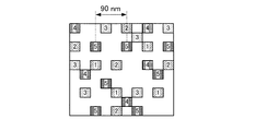
- FIG. 2C illustrates a mask pattern after division according to one embodiment.
- FIG. 3 illustrates a sequence of preparing a conflict graph.
- the present disclosure is applied when generating pattern data for a mask (original) used in a micromechanism or manufacture of various types of devices such as an imaging element, or the like such as a CCD, a detection element such as a magnetic head, or the like, a display element such as a liquid panel, or the like, or a semiconductor chip such as an IC, LSI, or the like.
- an imaging element or the like such as a CCD
- a detection element such as a magnetic head, or the like
- a display element such as a liquid panel, or the like
- semiconductor chip such as an IC, LSI, or the like.
- FIG. 1 illustrates a flowchart illustrating the flow of generation of mask data according to one exemplary embodiment.
- the generating method according to the present exemplary embodiment is executed by an information processing apparatus such as a computer, to thereby generate mask data used in an exposure apparatus configured to expose a mask pattern image on a substrate.
- the computer obtains pattern data for the object to be divided (step S100).
- FIGs. 2A to 2C illustrate a mask pattern before division and after division.
- FIG. 2A illustrates a pattern for an object to be divided (before division).
- the pattern of the object to be divided is provided for example in a polygonal coordinate format.
- FIG. 3 is a schematic figure that illustrates a sequence of preparing a conflict graph by use of the polygonal data.
- the term "disposition limitation conditions for the pattern" denotes the feature in which a distance 10 between central positions of individual patterns is defined, and when the distance 10 is within a predetermined distance, the conditions must be denoted by different mask numbers.
- the mask numbers are the individual numbers that correspond to respective masks such as 1, 2, 3, or the like, and may be referred to as color numbers in relation to the coloring problem. Furthermore, the division into different mask numbers is termed coating division in the coloring problem.
- step S102 the computer executes determining formulation of the disposition limitation condition by stating the disposition limitation condition determined in the step S101 as an integer problem.
- step S103 the computer analyzes the distance between the pattern elements.
- step S104 the computer executes determining formulation of the limitation conditions by stating the limitation conditions for the distance between the pattern elements as an integer problem.
- the computer minimizes the number of divisions of the mask pattern and uses a cost function that maximizes the minimum value for the distance between pattern elements to thereby divide the mask pattern using a mathematical programming method (step S105), and thereby completes generation of the mask data corresponding to each mask.
- step S105 solver software called ILOG CPLEX (registered trademark) of the IBM Corporation for example is used to realize the mathematical programming method.
- ILOG CPLEX registered trademark of the IBM Corporation
- the reduction to an equation executed in the steps S102 and S104 are stated in a 1p file.
- the equation for the integer problem used in the steps S102 and S104 when solving by use of a mathematical programming method will be described below.
- the variable m denotes the maximum mask number.
- the variable y j denotes a binary variable that expresses whether or not the mask number j is used, and takes a value of 1 when the mask number j is used and a value of 0 when the mask number j is not used.
- the variable i denotes the number of the pattern element (the mask pattern number).
- the variable x ij denotes a binary variable that expresses whether or not the mask number j is used in relation to the number i of the pattern element, and takes a value of 1 when the mask number j is used and a value of 0 when the mask number j is not used.
- P all denotes the minimum value of the distance between patterns for all mask numbers.
- P j denotes the minimum value of the distance between patterns in relation to the j-th mask number.
- D ii'j denotes a binary variable that takes a value of 1 when both of the i-th pattern and the i'-th pattern use the j-th mask, and when this is not the case, takes a value of 0.
- the constant pitch ii' denotes the interval between the i-th pattern element and the i'-th pattern element.
- the constant alpha denotes a weighting for the cost function for the number of the mask numbers (color number).
- the constant beta denotes a weighting for the cost function for the distance between pattern elements for all masks.
- the constant gamma denotes a weighting for the cost function for the distance between pattern elements for the j-th mask.
- Equation 1 The cost function (objective function) is expressed in a polynomial form as illustrated in Equation 1.
- Equation 1 expresses that the number of used mask numbers is minimized, and the minimum value of the distance between pattern elements is maximized. Furthermore, the first term in Equation 1 expresses the number of mask numbers, and the second term and third term express the minimum value of the distance between pattern elements for the same mask number. In addition, the portion (first variable) that is not multiplied by alpha in the first term in Equation 1 is expressed by Equation 2.
- Equation 2 is equal to the number of mask numbers, and for example, when the number of mask numbers is increased by a value of 1 from 2 to 3, the value of Equation 2 also increases from 2 to 3.
- P all (second variable) expresses the minimum value (nm) of the distance between divided patterns
- P all is reduced by a value of one. Since the generation of the mask data according to the present embodiment includes division of the mask pattern by the lowest number of mask numbers, and increasing (maximizing) the distance between pattern elements to the greatest degree possible, the weighting in the first term of Equation 1 must be made as large as possible.
- the absolute value of alpha must be sufficiently large in comparison to the absolute value of beta and gamma.
- beta takes a value of approximately -0.001.
- the third term in Equation 1 is a term for maximizing the minimum value of the distance between pattern elements for individual mask numbers after maximizing the distance between patterns for all mask numbers.
- the third term may not be a required term in light of generation of lithography friendly mask data.
- the optimal cost function may be written as maximizing the number of mask numbers that are used.
- the cost function is expressed by Equation 3, wherein alpha is a negative constant, and beta and gamma are both positive constants.
- Equation 5 expresses limitation conditions such that only one mask number is used in relation to the flag x i of the i-th mask pattern. For example, the first mask number and the second mask number are not used in relation to the i-th pattern.
- Equation 6 expresses limitation conditions such that division is not allowable in relation to mask numbers that are not used.
- Equation 7 expresses a limitation condition for a pattern based on the conflict graph, and is applied when the i-th pattern is connected to the i'-th pattern by a line segment, that is to say, when the same mask number cannot be used.
- Equation 12 is the equation used in step S102, and is the boundary condition that expresses use of the 1-th mask number.
- Equation 13 and Equation 14 are both used in step S104.
- Equation 13 is the boundary condition that expresses that the distance of each mask number is a value that is greater than 0.
- Equation 14 is the boundary condition that expresses that the minimum value of the distance between pattern elements is a value greater than 0.
- Equation 15 to Equation 17 are all binary variables and fluctuate in the range ⁇ 0, 1 ⁇ .
- FIG. 2B illustrates map data for the pattern illustrated in FIG. 2A when a mask pattern division is performed that does not consider the minimum value between the pattern distances.
- FIG. 2C applies the mask data generating method according to the present exemplary embodiment and illustrates map data in relation to the pattern illustrated in FIG. 2A when a mask pattern division is performed that considers the minimum value between the pattern distances.
- the numbers stated in FIG. 2B and FIG. 2C are the divided mask numbers.
- 2A includes a grid in the x direction and the y direction that has a 30 nm pitch, and the minimum value of the distance between pattern elements is 42 nm.
- This pattern is subjected to pattern division so that a pattern within 85 nm has a different mask number.
- the minimum value between the pattern elements is not considered, as illustrated in FIG. 2B, the minimum value for the distance between the pattern elements is 90 nm, and the number of mask pattern divisions is 5.
- the minimum value between the pattern elements is considered, as illustrated in FIG. 2C, the minimum value for the distance between the pattern elements is 120 nm, and the number of mask pattern divisions is 5.
- the present exemplary embodiment provides a lithography friendly mask data generating method that maximizes the minimum value of the distance between pattern elements of the divided pattern and reduces the number of mask pattern divisions.
- the mask data generating method according to the present exemplary embodiment uses an integer programming.
- another optimization method may be used as long as it is a method that simultaneously expresses a first variable that denotes the mask division number and a second variable that denotes the minimum value for distances between common pattern elements as a cost function.
- a method such as a genetic algorithm or a mixed integer programming may be used.
- the present disclosure may be realized by execution of the following processing steps. That is to say, the software (program) that realizes the functions in the above exemplary embodiment is supplied to a system or an apparatus through various types of storage media, and the computer (information processing apparatus) of the system or the apparatus performs processing by reading and executing the program.
- a mask drawing apparatus manufactures a plurality of masks by inputting mask data generated by use of the generating method according to the above exemplary embodiment into the mask drawing apparatus.
- the manufactured masks are mounted onto a mask stage in the exposure apparatus, and illuminated by an illumination optical system to thereby expose an image of a pattern on the mask onto a wafer.
- wafer exposure is executed using another mask in relation to the same layer of the wafer, and thereby it is possible to form a pattern on one layer on the wafer using a plurality of exposure operations.
- the liquid crystal display device is manufactured using a process of forming a transparent electrode.
- the process of forming a transparent electrode includes a step of applying a photosensitive agent onto a glass substrate that is subjected to vapor deposition of a transparent conductive film, a step of exposing the glass substrate that is coated with the photosensitive agent after mounting of a mask manufactured as described above in an exposure apparatus, and a step of developing the glass substrate.
- the device manufacturing method using the exposure apparatus as described above is applicable to the manufacture of a device such as a semiconductor device for example, in addition to a liquid crystal display device.
- the above method may includes a step of mounting a mask manufactured as described above in an exposure apparatus and exposing a substrate that is coated with the photosensitive agent, and a step of developing the exposed substrate.
- the method of manufacture of a device may include other known steps (oxidation, film deposition, vapor deposition, doping, flattening, etching, resist peeling, dicing, bonding, and packaging, or the like).
Landscapes
- Physics & Mathematics (AREA)
- General Physics & Mathematics (AREA)
- Engineering & Computer Science (AREA)
- Computer Hardware Design (AREA)
- Theoretical Computer Science (AREA)
- Evolutionary Computation (AREA)
- Geometry (AREA)
- General Engineering & Computer Science (AREA)
- Preparing Plates And Mask In Photomechanical Process (AREA)
- Exposure And Positioning Against Photoresist Photosensitive Materials (AREA)
Description










Claims (9)
- A mask data generating method for generating data of a plurality of masks used in a plurality of exposures in which exposure light is irradiated onto a substrate using a mask, and then exposure light is irradiated onto the substrate using another mask, the method comprising the following steps executed by a computer:
obtaining data for a pattern including a plurality of pattern elements,
determining formulation of a disposition limitation condition for the pattern elements,
analyzing the distance between the pattern elements,
determining formulation of the distance limitation condition, and
applying a first variable configured to express a number of pattern divisions and a second variable configured to express a distance related to all pattern elements in a cost function and thereby dividing the pattern. - The mask data generating method according to claim 1, wherein a minimum value of the distances related to a plurality of the patterns is used as the cost function.
- The mask data generating method according to claim 1, wherein the disposition limitation condition, the distance limitation condition and the cost function are stated as an integer problem, and in the dividing the pattern, an integer programming or a mixed integer programming is used.
- The mask data generating method according to claim 1, wherein the coefficient multiplied by the first variable is a positive constant, the coefficient multiplied by the second variable is a negative constant, the cost function is expressed as a polynomial that includes the above two terms and the pattern is divided by minimizing the cost function.
- The mask data generating method according to claim 1, wherein the coefficient multiplied by the first variable is a negative constant, the coefficient multiplied by the second variable is a positive constant, the cost function is expressed as a polynomial that includes the above two terms and the pattern is divided by maximizing the cost function.
- A storage medium storing a computer program, wherein the computer program causes the computer to execute the mask data generating method according to claim 1.
- An information processing apparatus configured to execute the mask data generating method according to claim 1.
- A mask manufacturing method, the method comprising:
generating the data of a plurality of masks using the mask data generating method according to claim 1, and
manufacturing the plurality of masks using the data. - A method for manufacturing a device, the method comprising:
transferring a pattern of the mask manufactured by mask manufacturing method according to claim 8, onto a substrate by use of the exposure apparatus, and
developing the substrate after transfer.
Priority Applications (3)
| Application Number | Priority Date | Filing Date | Title |
|---|---|---|---|
| CN201380045839.0A CN104641290A (en) | 2012-09-06 | 2013-09-03 | Mask data generation method, program for executing the method, and information processing device |
| KR1020157004965A KR20150038373A (en) | 2012-09-06 | 2013-09-03 | Mask data generating method, program and information processing apparatus for execution of the same |
| US14/416,762 US9569576B2 (en) | 2012-09-06 | 2013-09-03 | Mask pattern generating method, storage medium, information processing apparatus for execution of the same, mask manufacturing method and device manufacturing method |
Applications Claiming Priority (2)
| Application Number | Priority Date | Filing Date | Title |
|---|---|---|---|
| JP2012195820A JP6140954B2 (en) | 2012-09-06 | 2012-09-06 | Mask data creation method, program for executing the method, and information processing apparatus |
| JP2012-195820 | 2012-09-06 |
Publications (1)
| Publication Number | Publication Date |
|---|---|
| WO2014038181A1 true WO2014038181A1 (en) | 2014-03-13 |
Family
ID=50236810
Family Applications (1)
| Application Number | Title | Priority Date | Filing Date |
|---|---|---|---|
| PCT/JP2013/005193 Ceased WO2014038181A1 (en) | 2012-09-06 | 2013-09-03 | Mask data generating method, program and information processing apparatus for execution of the same |
Country Status (6)
| Country | Link |
|---|---|
| US (1) | US9569576B2 (en) |
| JP (1) | JP6140954B2 (en) |
| KR (1) | KR20150038373A (en) |
| CN (1) | CN104641290A (en) |
| TW (1) | TW201413486A (en) |
| WO (1) | WO2014038181A1 (en) |
Families Citing this family (6)
| Publication number | Priority date | Publication date | Assignee | Title |
|---|---|---|---|---|
| JP5665915B2 (en) * | 2012-06-05 | 2015-02-04 | キヤノン株式会社 | How to create mask data |
| US9842185B2 (en) * | 2015-08-21 | 2017-12-12 | Qualcomm Incorporated | Systems and methods for group constraints in an integrated circuit layout |
| US10671786B2 (en) * | 2016-11-29 | 2020-06-02 | Taiwan Semiconductor Manufacturing Co., Ltd. | Method of modeling a mask by taking into account of mask pattern edge interaction |
| US10885224B2 (en) | 2018-02-01 | 2021-01-05 | International Business Machines Corporation | Data de-identification with minimal data change operations to maintain privacy and data utility |
| US10831928B2 (en) * | 2018-06-01 | 2020-11-10 | International Business Machines Corporation | Data de-identification with minimal data distortion |
| CN121634685A (en) * | 2026-02-03 | 2026-03-10 | 合肥晶合集成电路股份有限公司 | Mask plate, pattern forming method and preparation method of semiconductor device |
Citations (5)
| Publication number | Priority date | Publication date | Assignee | Title |
|---|---|---|---|---|
| JP2007183630A (en) * | 2005-12-29 | 2007-07-19 | Asml Masktools Bv | Method, program product and apparatus for model-based geometry decomposition used in multiple exposure processes |
| JP2009053605A (en) * | 2007-08-29 | 2009-03-12 | Renesas Technology Corp | Semiconductor device manufacturing method and mask |
| JP2009200499A (en) * | 2008-02-22 | 2009-09-03 | Interuniv Micro Electronica Centrum Vzw | Split and design guideline for double patterning |
| JP2010123943A (en) * | 2008-11-11 | 2010-06-03 | Asml Netherlands Bv | Method, program product and apparatus for performing model based coloring process for pattern decomposition for use in multiple exposure process |
| JP2012220955A (en) * | 2011-04-04 | 2012-11-12 | Asml Netherlands Bv | Integration of lithography apparatus and mask optimization process including multiple patterning process |
Family Cites Families (3)
| Publication number | Priority date | Publication date | Assignee | Title |
|---|---|---|---|---|
| US8132130B2 (en) | 2005-06-22 | 2012-03-06 | Asml Masktools B.V. | Method, program product and apparatus for performing mask feature pitch decomposition for use in a multiple exposure process |
| US7794903B2 (en) | 2006-08-15 | 2010-09-14 | Infineon Technologies Ag | Metrology systems and methods for lithography processes |
| US8402396B2 (en) | 2009-09-29 | 2013-03-19 | The Regents Of The University Of California | Layout decomposition for double patterning lithography |
-
2012
- 2012-09-06 JP JP2012195820A patent/JP6140954B2/en not_active Expired - Fee Related
-
2013
- 2013-09-03 KR KR1020157004965A patent/KR20150038373A/en not_active Withdrawn
- 2013-09-03 CN CN201380045839.0A patent/CN104641290A/en not_active Withdrawn
- 2013-09-03 WO PCT/JP2013/005193 patent/WO2014038181A1/en not_active Ceased
- 2013-09-03 US US14/416,762 patent/US9569576B2/en not_active Expired - Fee Related
- 2013-09-05 TW TW102131981A patent/TW201413486A/en unknown
Patent Citations (5)
| Publication number | Priority date | Publication date | Assignee | Title |
|---|---|---|---|---|
| JP2007183630A (en) * | 2005-12-29 | 2007-07-19 | Asml Masktools Bv | Method, program product and apparatus for model-based geometry decomposition used in multiple exposure processes |
| JP2009053605A (en) * | 2007-08-29 | 2009-03-12 | Renesas Technology Corp | Semiconductor device manufacturing method and mask |
| JP2009200499A (en) * | 2008-02-22 | 2009-09-03 | Interuniv Micro Electronica Centrum Vzw | Split and design guideline for double patterning |
| JP2010123943A (en) * | 2008-11-11 | 2010-06-03 | Asml Netherlands Bv | Method, program product and apparatus for performing model based coloring process for pattern decomposition for use in multiple exposure process |
| JP2012220955A (en) * | 2011-04-04 | 2012-11-12 | Asml Netherlands Bv | Integration of lithography apparatus and mask optimization process including multiple patterning process |
Also Published As
| Publication number | Publication date |
|---|---|
| CN104641290A (en) | 2015-05-20 |
| TW201413486A (en) | 2014-04-01 |
| JP6140954B2 (en) | 2017-06-07 |
| US20150213175A1 (en) | 2015-07-30 |
| KR20150038373A (en) | 2015-04-08 |
| US9569576B2 (en) | 2017-02-14 |
| JP2014052474A (en) | 2014-03-20 |
Similar Documents
| Publication | Publication Date | Title |
|---|---|---|
| WO2014038181A1 (en) | Mask data generating method, program and information processing apparatus for execution of the same | |
| US8046722B2 (en) | Method for correcting a mask pattern, system for correcting a mask pattern, program, method for manufacturing a photomask and method for manufacturing a semiconductor device | |
| US8037427B2 (en) | Method for manufacturing a photomask | |
| JP5529391B2 (en) | Halftone phase shift mask, semiconductor device manufacturing apparatus having the halftone phase shift mask, and semiconductor device manufacturing method using the halftone phase shift mask | |
| US9754068B2 (en) | Method, computer readable storage medium and computer system for creating a layout of a photomask | |
| CN104007608A (en) | Method for determining mask pattern, non-transitory recording medium, and information processing apparatus | |
| CN109656106B (en) | Processing method and device for mask in computational lithography | |
| CN113495424A (en) | Optical proximity correction method and manufacturing method of mask | |
| CN116520632B (en) | Layout correction method, storage medium and terminal | |
| CN114326290A (en) | Optical proximity correction method | |
| KR102556509B1 (en) | Method for rasterization of mask layout and method of fabricating photomask using the same | |
| US7793253B2 (en) | Mask-patterns including intentional breaks | |
| CN116203803A (en) | Method for optical proximity correction and method for manufacturing semiconductor device | |
| CN114063380B (en) | Pattern correction method and semiconductor structure forming method | |
| US9547230B2 (en) | Method for evaluating optical image of pattern, recording medium, and information processing apparatus | |
| JP2014102292A (en) | Photomask, division exposure method, and method for manufacturing a semiconductor device | |
| US10282487B2 (en) | Mask data generation method | |
| US20250244662A1 (en) | Photomask pattern inspection method and system, and method of manufacturing display device using the same | |
| CN116413991B (en) | Optical proximity correction method | |
| US20240427231A1 (en) | Optical proximity correction method and mask manufacturing method by using the same | |
| CN119620526A (en) | Auxiliary graphics adding method, system and terminal | |
| KR20130136922A (en) | Mask data generation method | |
| US9152037B2 (en) | Pattern correction method, storage medium, information processing apparatus, method of manufacturing mask, exposure apparatus, and method of manufacturing device | |
| TW202347014A (en) | System, method and program product for improving accuracy of photomask based compensation in flat panel display lithography | |
| CN120129872A (en) | Method and apparatus for generating pattern density data |
Legal Events
| Date | Code | Title | Description |
|---|---|---|---|
| 121 | Ep: the epo has been informed by wipo that ep was designated in this application |
Ref document number: 13834710 Country of ref document: EP Kind code of ref document: A1 |
|
| WWE | Wipo information: entry into national phase |
Ref document number: 14416762 Country of ref document: US |
|
| ENP | Entry into the national phase |
Ref document number: 20157004965 Country of ref document: KR Kind code of ref document: A |
|
| NENP | Non-entry into the national phase |
Ref country code: DE |
|
| 122 | Ep: pct application non-entry in european phase |
Ref document number: 13834710 Country of ref document: EP Kind code of ref document: A1 |