WO2013183531A1 - 表示装置およびその駆動方法 - Google Patents
表示装置およびその駆動方法 Download PDFInfo
- Publication number
- WO2013183531A1 WO2013183531A1 PCT/JP2013/064998 JP2013064998W WO2013183531A1 WO 2013183531 A1 WO2013183531 A1 WO 2013183531A1 JP 2013064998 W JP2013064998 W JP 2013064998W WO 2013183531 A1 WO2013183531 A1 WO 2013183531A1
- Authority
- WO
- WIPO (PCT)
- Prior art keywords
- voltage
- power supply
- gate
- display
- tft
- Prior art date
- Legal status (The legal status is an assumption and is not a legal conclusion. Google has not performed a legal analysis and makes no representation as to the accuracy of the status listed.)
- Ceased
Links
Images



Classifications
-
- G—PHYSICS
- G02—OPTICS
- G02F—OPTICAL DEVICES OR ARRANGEMENTS FOR THE CONTROL OF LIGHT BY MODIFICATION OF THE OPTICAL PROPERTIES OF THE MEDIA OF THE ELEMENTS INVOLVED THEREIN; NON-LINEAR OPTICS; FREQUENCY-CHANGING OF LIGHT; OPTICAL LOGIC ELEMENTS; OPTICAL ANALOGUE/DIGITAL CONVERTERS
- G02F1/00—Devices or arrangements for the control of the intensity, colour, phase, polarisation or direction of light arriving from an independent light source, e.g. switching, gating or modulating; Non-linear optics
- G02F1/01—Devices or arrangements for the control of the intensity, colour, phase, polarisation or direction of light arriving from an independent light source, e.g. switching, gating or modulating; Non-linear optics for the control of the intensity, phase, polarisation or colour
- G02F1/13—Devices or arrangements for the control of the intensity, colour, phase, polarisation or direction of light arriving from an independent light source, e.g. switching, gating or modulating; Non-linear optics for the control of the intensity, phase, polarisation or colour based on liquid crystals, e.g. single liquid crystal display cells
- G02F1/133—Constructional arrangements; Operation of liquid crystal cells; Circuit arrangements
-
- G—PHYSICS
- G09—EDUCATION; CRYPTOGRAPHY; DISPLAY; ADVERTISING; SEALS
- G09G—ARRANGEMENTS OR CIRCUITS FOR CONTROL OF INDICATING DEVICES USING STATIC MEANS TO PRESENT VARIABLE INFORMATION
- G09G3/00—Control arrangements or circuits, of interest only in connection with visual indicators other than cathode-ray tubes
- G09G3/20—Control arrangements or circuits, of interest only in connection with visual indicators other than cathode-ray tubes for presentation of an assembly of a number of characters, e.g. a page, by composing the assembly by combination of individual elements arranged in a matrix no fixed position being assigned to or needed to be assigned to the individual characters or partial characters
- G09G3/34—Control arrangements or circuits, of interest only in connection with visual indicators other than cathode-ray tubes for presentation of an assembly of a number of characters, e.g. a page, by composing the assembly by combination of individual elements arranged in a matrix no fixed position being assigned to or needed to be assigned to the individual characters or partial characters by control of light from an independent source
- G09G3/36—Control arrangements or circuits, of interest only in connection with visual indicators other than cathode-ray tubes for presentation of an assembly of a number of characters, e.g. a page, by composing the assembly by combination of individual elements arranged in a matrix no fixed position being assigned to or needed to be assigned to the individual characters or partial characters by control of light from an independent source using liquid crystals
- G09G3/3611—Control of matrices with row and column drivers
- G09G3/3648—Control of matrices with row and column drivers using an active matrix
-
- G—PHYSICS
- G09—EDUCATION; CRYPTOGRAPHY; DISPLAY; ADVERTISING; SEALS
- G09G—ARRANGEMENTS OR CIRCUITS FOR CONTROL OF INDICATING DEVICES USING STATIC MEANS TO PRESENT VARIABLE INFORMATION
- G09G3/00—Control arrangements or circuits, of interest only in connection with visual indicators other than cathode-ray tubes
- G09G3/20—Control arrangements or circuits, of interest only in connection with visual indicators other than cathode-ray tubes for presentation of an assembly of a number of characters, e.g. a page, by composing the assembly by combination of individual elements arranged in a matrix no fixed position being assigned to or needed to be assigned to the individual characters or partial characters
-
- G—PHYSICS
- G09—EDUCATION; CRYPTOGRAPHY; DISPLAY; ADVERTISING; SEALS
- G09G—ARRANGEMENTS OR CIRCUITS FOR CONTROL OF INDICATING DEVICES USING STATIC MEANS TO PRESENT VARIABLE INFORMATION
- G09G3/00—Control arrangements or circuits, of interest only in connection with visual indicators other than cathode-ray tubes
- G09G3/20—Control arrangements or circuits, of interest only in connection with visual indicators other than cathode-ray tubes for presentation of an assembly of a number of characters, e.g. a page, by composing the assembly by combination of individual elements arranged in a matrix no fixed position being assigned to or needed to be assigned to the individual characters or partial characters
- G09G3/34—Control arrangements or circuits, of interest only in connection with visual indicators other than cathode-ray tubes for presentation of an assembly of a number of characters, e.g. a page, by composing the assembly by combination of individual elements arranged in a matrix no fixed position being assigned to or needed to be assigned to the individual characters or partial characters by control of light from an independent source
- G09G3/36—Control arrangements or circuits, of interest only in connection with visual indicators other than cathode-ray tubes for presentation of an assembly of a number of characters, e.g. a page, by composing the assembly by combination of individual elements arranged in a matrix no fixed position being assigned to or needed to be assigned to the individual characters or partial characters by control of light from an independent source using liquid crystals
-
- G—PHYSICS
- G09—EDUCATION; CRYPTOGRAPHY; DISPLAY; ADVERTISING; SEALS
- G09G—ARRANGEMENTS OR CIRCUITS FOR CONTROL OF INDICATING DEVICES USING STATIC MEANS TO PRESENT VARIABLE INFORMATION
- G09G2310/00—Command of the display device
- G09G2310/02—Addressing, scanning or driving the display screen or processing steps related thereto
- G09G2310/0243—Details of the generation of driving signals
- G09G2310/0245—Clearing or presetting the whole screen independently of waveforms, e.g. on power-on
-
- G—PHYSICS
- G09—EDUCATION; CRYPTOGRAPHY; DISPLAY; ADVERTISING; SEALS
- G09G—ARRANGEMENTS OR CIRCUITS FOR CONTROL OF INDICATING DEVICES USING STATIC MEANS TO PRESENT VARIABLE INFORMATION
- G09G2330/00—Aspects of power supply; Aspects of display protection and defect management
- G09G2330/02—Details of power systems and of start or stop of display operation
- G09G2330/027—Arrangements or methods related to powering off a display
Definitions
- the present invention relates to a display device, and more particularly, to a technique for discharging charges accumulated in each display pixel when a power interruption occurs.
- a liquid crystal display device is known as an example of a display device.
- a liquid crystal display device a system in which a plurality of pixel electrodes are driven by thin film transistors (TFTs) is widely adopted.
- TFTs thin film transistors
- Such a method is called an active matrix method.
- Such an active matrix type liquid crystal display device includes a gate wiring arranged on a substrate for supplying a signal to a thin film transistor, and a plurality of source wirings arranged above the gate wiring so as to cross the gate wiring.
- Patent Document 1 discloses a display in which a plurality of display pixels are two-dimensionally arranged in the vicinity of intersections of a plurality of gate lines and a plurality of source lines arranged orthogonal to each other.
- a display device including a source driver for applying a display signal voltage is disclosed.
- a display device generates a plurality of drive voltages defining at least the voltage levels of a scanning signal and a display signal voltage based on a predetermined drive power, and a gate driver And a power supply voltage supply circuit for supplying the source driver.
- the power supply voltage supply circuit generates a drive voltage having a ground potential and supplies it to the gate driver when the supply of drive power is cut off due to the power supply battery dropping off or the like.
- a scanning signal having a ground potential is supplied to all the gate wirings constituting the display panel, all the display pixels are set to a selected state, and the electric charge accumulated in each display pixel is set to a predetermined potential (common signal). Voltage).
- the power supply voltage supply circuit uses a negative voltage as a drive voltage to the gate driver in a state in which display drive is performed in which drive power is normally supplied from the power supply battery.
- the driving voltage having a negative voltage is quickly transferred to the ground potential, and the pixel transistor (pixel TFT) provided in each display pixel
- the voltage level of the scanning signal applied to the gate wiring is controlled so as to turn on. As a result, the electric charge accumulated in each display pixel is discharged, and the occurrence of an afterimage in which the display image gradually disappears with the occurrence of power interruption is suppressed.
- a turn-on operation of the pixel transistor can be promoted by applying a scanning signal having a positive voltage to the pixel transistor due to the characteristics of the TFT.
- a scanning signal having a positive voltage to the pixel transistor due to the characteristics of the TFT.
- Patent Document 1 described above, even in the case where a power interruption occurs, the configuration for controlling the voltage level of the scanning signal applied from the gate driver to the gate wiring is controlled according to the specifications of the gate driver. The voltage level of possible scanning signals is limited. As a result, it has been difficult to quickly discharge the charge accumulated in each display pixel.
- the present invention has been made to solve such problems, and an object of the present invention is to quickly store charges accumulated in each display pixel when a power interruption occurs in an active matrix display device. It is to discharge.
- a display device includes a plurality of gate wirings and a plurality of source wirings arranged orthogonal to each other, and a plurality of display devices arranged corresponding to intersections of the plurality of gate wirings and the plurality of source wirings.
- a display panel including a display pixel, a gate driver that sets each display pixel to a selected state by sequentially applying a scanning signal to a plurality of gate wirings, and a selected state through each source wiring
- a source driver that applies a display signal voltage to a display pixel, and a power supply voltage that generates a drive voltage having a voltage level that sets at least the display pixel to a selected state using a power supply voltage supplied from the power supply and supplies the drive voltage to the gate driver
- a generator, a monitoring unit that monitors the power supply voltage, and a plurality of gate wirings and a power supply voltage generating unit are provided, respectively.
- the active matrix display device it is possible to quickly discharge the electric charge accumulated in each display pixel when the power is cut off.
- FIG. 2 is a configuration diagram of an analog power supply generation unit, a power supply monitoring circuit, and a SW_TFT control signal generation unit shown in FIG. 1. It is a figure explaining operation
- FIG. It is a block diagram which shows one Embodiment of the liquid crystal display device to which the display apparatus by Embodiment 2 of this invention is applied. It is a figure which shows the time change of the voltage applied to pixel TFT and switch TFT.
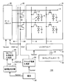
- FIG. 1 is a block diagram showing an embodiment of a liquid crystal display device to which a display device according to Embodiment 1 of the present invention is applied.
- a liquid crystal display device 100 includes a display panel 10 in which a plurality of display pixels 1 are arranged in a matrix, a gate driver 20, a source driver 30, a timing controller 40, a power supply 50, an analog, and the like.
- a power generation unit 60 is provided.
- the display panel 10 includes a plurality of gate wirings 12 and a plurality of source wirings 14, a plurality of gate wirings 12, and a plurality of source wirings 14 that are disposed between opposing transparent substrates (not shown). And a plurality of display pixels 1 arranged corresponding to the intersections.
- Each display pixel 1 includes a pixel electrode 4, an auxiliary capacitance electrode 6, and a thin film transistor (TFT) 2.
- the TFT 2 has a drain electrode connected to the pixel electrode 4, a source electrode connected to the source wiring 14, and a gate electrode connected to the gate wiring 12.
- the display pixel 1 is connected in parallel to a liquid crystal capacitor composed of liquid crystal molecules filled and held between the pixel electrode 4 and a common electrode (counter electrode) disposed opposite to the pixel electrode 4, And a storage capacitor for holding a signal voltage applied to the liquid crystal capacitor.
- the gate driver 20 sequentially scans the display pixel group in each row of the display panel 10 and sets it to the selected state.
- the source driver 30 collectively outputs display signal voltages based on the video signal to the display pixel group in the row set to the selected state.
- the gate driver 20 sequentially applies a scanning signal (hereinafter also referred to as “gate driver output”) to the plurality of gate wirings 12 to set the display pixel group in each row to a selected state.
- the source driver 30 applies a display signal voltage (hereinafter also referred to as “source driver output”) to each display pixel 1 via each source line 14 in synchronization with the timing at which the display pixel group in each row is selected. Supply all at once.
- a common signal voltage Vcom having an inverted polarity with respect to the display signal voltage is applied to the counter electrode.
- the timing controller 40 controls the operation timing of the gate driver 20 and the source driver 30 based on a video signal input from the outside of the apparatus. Note that the timing controller 40 and the source driver 30 are connected via a data signal line 32 constituted by a pair of operation signal lines. A differential digital data signal is supplied from the timing controller 40 to the source driver 30 via the data signal line 32.
- the desired image information based on the video signal is displayed on the display panel 10 by repeatedly executing the series of operations described above for each row for one screen.
- the TFT 2 is used as a switching element (hereinafter also referred to as “pixel transistor”) for supplying a display signal voltage to the pixel electrode 4, hereinafter, the TFT 2 is referred to as “pixel TFT (or , LCD_TFT) ”.
- the power supply 50 is a DC power supply whose negative electrode side is connected to the ground voltage (0 V), and supplies a power supply voltage Vpower (for example, 3.3 V) to the gate driver 20, source driver 30, and analog power supply generation unit 60. To do.
- Vpower for example, 3.3 V
- the analog power generation unit 60 uses the power supply voltage Vpower supplied from the power supply 50 to generate a drive voltage necessary for display driving of the display panel 10. For example, the analog power supply generation unit 60 generates the drive voltage VGH from the power supply voltage Vpower and supplies it to the gate driver 20.
- the gate driver 20 is based on the drive voltage VGH supplied from the analog power supply generation unit 60, the voltage (ON voltage: positive voltage) VGH that defines the high level of the scanning signal, and the voltage that defines the low level of the scanning signal ( Off-voltage: negative voltage) VGL.
- the display device 100 performs the display drive of the image information described above based on the power supply voltage Vpower supplied from the power supply 50.
- the power supply voltage Vpower supplied from the power supply 50 to the gate driver 20, the source driver 30 and the analog power supply generation unit 60 shifts to the ground voltage.
- the drive voltage VGH supplied from the analog power generation unit 60 to the gate driver 20 also gradually shifts to the ground voltage.
- the drive voltage VGH reaches the ground voltage at a speed slower than the power supply voltage Vpower due to free discharge of the capacitor and load capacitance provided in the analog power supply generation unit 60.
- the scanning signal applied to the gate wiring 12 is set to the off voltage VGL (negative voltage) after the power supply is cut off.
- VGL negative voltage
- the pixel TFT2 is controlled to be in an OFF state, so that charges accumulated in each display pixel (liquid crystal capacitor, storage capacitor) for displaying image information are held.
- the scanning drive of the display panel 10 is stopped for a relatively long time after the power supply is cut off, and the accumulated charge is held in the display pixel 1, and the image information is gradually increased along with the discharge of the accumulated charge. An afterimage disappears. Thereby, display quality deteriorates.
- the display device 100 includes a SW_TFT block 90 disposed adjacent to the display panel 10 in the row direction as a configuration for discharging the accumulated charge of each display pixel 1 after the power is shut off, A monitoring circuit 70 and a SW_TFT control signal generation unit 80 are further provided.
- the SW_TFT block 90 includes a plurality of TFTs 92 arranged in the column direction of the display panel 10, and gate wirings 94 and source wirings 96 arranged in parallel with the plurality of source wirings 14.
- Each TFT 92 is disposed at the intersection of each gate line 12 and source line 96.
- the TFT 92 has a drain connected to the gate wiring 12, a source connected to the source wiring 96, and a gate connected to the gate wiring 94.
- the TFT 92 is formed on the same substrate as the pixel TFT 2 included in the display pixel 1.
- the TFT 92 can be integrally formed with the same structure and the same process as the pixel TFT 2.
- the gate wiring 94 is connected to the SW_TFT control signal generation unit 80.
- the gate wiring 94 applies a control signal supplied from the SW_TFT control signal generation unit 80 to the gate of the TFT 92.
- the source wiring 96 is connected to the analog power supply generation unit 60. As shown in FIG. 1, the drive voltage VGH generated by the analog power supply generation unit 60 is supplied to the gate driver 20 and the source wiring 96.
- the source wiring 96 applies the supplied drive voltage VGH to the source of the TFT 92.
- each TFT 92 included in the SW_TFT block 90 transmits the driving voltage VGH output from the analog power supply generation unit 60 to the gate wiring 12 when turned on in response to the control signal.
- the drive voltage VGH corresponds to the on-voltage (positive voltage) of the scanning signal output from the gate driver 20 during the display drive. Accordingly, the pixel TFT2 receives the drive voltage VGH (on voltage) and is driven to an on state.
- the TFT 92 is used as a transistor (hereinafter also referred to as “switch transistor”) for controlling the signal level of the scanning signal supplied to the gate wiring 12 instead of the gate driver 20.
- the TFT 92 is also referred to as “switch TFT (or SW_TFT)” in order to distinguish it from the pixel TFT 2.
- the power supply monitoring circuit 70 includes a detection circuit that detects the power supply voltage Vpower supplied from the power supply 50.
- the power monitoring circuit 70 generates a reference voltage Vref based on the detected value of the power supply voltage Vpower, and outputs the generated reference voltage Vref to the SW_TFT control signal generator 80.
- the reference voltage Vref generated by the power supply monitoring circuit 70 is variably set according to the voltage level of the power supply voltage Vpower. Specifically, when the voltage level of the power supply voltage Vpower is lowered, the reference voltage Vref is set low.
- the SW_TFT control signal generation unit 80 receives the drive voltage (VGH + ⁇ ) from the analog power supply generation unit 60 and the reference voltage Vref from the power supply monitoring circuit 70.
- the drive voltage (VGH + ⁇ ) corresponds to the output voltage of the charge pump circuit included in the analog power supply generation unit 60, as will be described later.
- the control signal generated by the SW_TFT control signal generation unit 80 is supplied to the gate wiring 94. That is, the voltage of the control signal is the gate voltage of the switch TFT 92 (hereinafter also referred to as “VG (SW_TFT)”).
- the analog power supply generation unit 60, the power supply monitoring circuit 70, and the SW_TFT control signal generation unit 80 will be further described.
- Analog power generation unit 60 includes a DC / DC converter 62, a charge pump circuit 64, a resistor R1, and a Zener diode ZD.
- the DC / DC converter 62 is configured by, for example, a boost chopper circuit.
- DC / DC converter 62 includes a reactor L1, a transistor Tr0, a diode D0, a capacitor C0, and a resistor R0.
- the transistor Tr0, the capacitor C0, and the resistor R0 are connected in parallel between the positive terminal and the negative terminal of the DC power source that constitutes the power source 50.
- Reactor L1 is connected between the positive terminal of the DC power supply and the collector of transistor Tr0.
- the diode D0 is connected between the collector of the transistor Tr0 and one end of the capacitor C0.
- the transistor Tr0 performs a switching operation in response to a switching command from a control unit (not shown), thereby generating a voltage V2 that is a voltage obtained by boosting the power supply voltage Vpower. More specifically, since the power supply voltage Vpower is short-circuited through the reactor L1 and a current flows during the ON period of the transistor Tr0, the magnetic flux level of the reactor L1 rises. During the off period of the transistor Tr0, a voltage is generated in the reactor L1, and the voltage is added to the power supply voltage Vpower, so that the diode D0 is turned on. As a result, the voltage V2 is raised from the power supply voltage Vpower. This voltage V2 is supplied to the charge pump circuit 64 together with the voltage V1 at the connection node of the reactor L1 and the diode D0.
- the charge pump circuit 64 includes capacitors C1, C2, C3 and diodes D1, D2.
- One end of capacitor C1 is connected to a connection node of reactor L1 and diode D0, and the other end is connected to an anode (anode) of diode D1 and a cathode (cathode) of diode D2.
- One end of the capacitor C2 is connected to the cathode of the diode D1, and the other end is connected to the anode of the diode D2.
- One end of the capacitor C3 is connected to the anode of the diode D2, and the other end is connected to the cathode of the diode D0 of the DC / DC converter 62.
- the charge pump circuit 64 receives the voltage V1 at one end of the capacitor C1 and the voltage V2 at the other end of the capacitor C3.
- the charge pump circuit 64 repeatedly performs a charging operation and a discharging operation in accordance with a difference between the voltage V2 and the voltage V1 that changes in a rectangular wave shape according to the switching operation of the transistor Tr0, whereby a predetermined voltage ⁇ is obtained from the driving voltage VGH.
- the charge pump circuit 64 outputs the generated drive voltage (VGH + ⁇ ) to the output line 66.
- a series circuit composed of a resistor R1 and a Zener diode ZD is connected between an output line 66 to which a drive voltage (VGH + ⁇ ) is applied and a ground node 8 to which a ground voltage (0 V) is applied.
- Zener diode ZD has a cathode connected to resistor R 1 and an anode connected to ground node 8.
- a connection node (corresponding to a node N1 in the drawing) of the resistor R1 and the Zener diode ZD constitutes an output node of the analog power supply generation unit 60.
- the output node N1 is electrically connected to the gate driver 20 and the source wiring 96 (FIG. 1).
- the Zener diode ZD uses the drive voltage VGH as the breakdown voltage. Therefore, the voltage of the Zener diode ZD is almost constant (drive voltage VGH) even if the reverse current changes. As a result, a constant voltage (drive voltage VGH) is output to the output node N1 of the analog power supply generation unit 60.
- the gate driver 20 generates an on-voltage of the scanning signal based on the driving voltage VGH. That is, the drive voltage VGH is the gate voltage of the pixel TFT 2 (hereinafter also referred to as “VG (LCD_TFT)”). Further, the drive voltage VGH is supplied to the source wiring 96 to become the source voltage of the switch TFT 92 (hereinafter also referred to as “VS (SW_TFT)”).
- SW_TFT control signal generator 80 is connected to the output line 66 of the charge pump circuit 64.
- SW_TFT control signal generator 80 includes a resistor R4 and a transistor Tr1 connected in series between output line 66 and ground node 8.
- the transistor Tr1 has a collector connected to the resistor R4, an emitter connected to the ground node 8, and a base connected to the output node (corresponding to the node N3 in the figure) of the power supply monitoring circuit 70.
- a connection node (corresponding to a node N2 in the drawing) of the resistor R4 and the transistor Tr1 constitutes an output node of the SW_TFT control signal generation unit 80.
- Power supply monitoring circuit 70 includes resistors R2 and R3 connected in series between power supply node 9 that receives power supply voltage Vpower from power supply 50 and ground node 8. Connection node N3 of resistors R2 and R3 constitutes an output node of power supply monitoring circuit 70.
- the power supply monitoring circuit 70 divides the power supply voltage Vpower to generate a reference voltage Vref proportional to the power supply voltage Vpower.
- the reference voltage Vref generated by the power supply monitoring circuit 70 is input to the base of the transistor Tr1 of the SW_TFT control signal generation unit 80 via the output node N3.
- the base-emitter voltage VBE when the transistor Tr1 is turned on is Vf (for example, 0.7V)
- Vref the reference voltage
- Vref> Vf the reference voltage
- the transistor Tr1 is turned on.
- a control signal having a ground voltage is output from the output node N2.
- the reference voltage Vref can be variably set by adjusting the resistance values of the resistors R2 and R3.
- determination value Vpower_th is set for power supply voltage Vpower.
- This determination value Vpower_th is a threshold value (for example, 2.7 V) for determining whether or not the power supply is shut off.
- the power supply monitoring circuit 70 compares the power supply voltage Vpower and the determination value Vpower_th, and detects power interruption based on the comparison result.
- the reference voltage Vref becomes higher than Vf, so that the transistor Tr1 is turned on and the SW_TFT control signal A control signal having a ground voltage is output from output node N2 of generation unit 80.
- the SW_TFT control signal generation unit 80 generates a control signal for controlling on / off of the switch TFT 92 by using the drive voltage (VGH + ⁇ ) generated by the analog power supply generation unit 60 and outputs the control signal to the gate wiring 94.
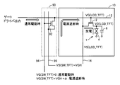
- FIG. 3 shows the display panel 10 and the SW_TFT block 90 extracted from the display device according to the first embodiment.
- one display pixel 1 is representatively shown in the display panel 10
- one switch TFT 92 is representatively shown in the SW_TFT block 90.
- a scanning signal (gate driver output) applied from gate driver 20 (FIG. 1) to gate wiring 12.
- the display signal voltage (source driver output) is applied to the display pixel 1 via the source line 14.
- a common signal voltage Vcom having an inverted polarity with respect to the display signal voltage is applied to the counter electrode.
- the power supply voltage Vpower and the drive voltage VGH supplied to the gate driver 20 shift to the ground voltage.
- the gate driver output is set to the drive voltage VGL. Since the drive voltage VGL corresponds to the off voltage (negative voltage) of the scanning signal, the pixel TFT 2 is controlled to be in the off state. Therefore, the charge accumulated in each display pixel 1 is held.
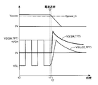
- FIG. 4 is a diagram showing temporal changes in voltages applied to the pixel TFT 2 and the switch TFT 92.
- the power supply voltage Vpower starts to decrease from the time when the power cut-off occurs (time t1) and the power supply voltage Vpower reaches the determination value Vpower_th at the subsequent time t2
- the drive voltage from the SW_TFT control signal generator 80 to the gate wiring 94 is set.
- a control signal having a voltage equal to (VGH + ⁇ ) is supplied.
- the gate voltage VG (SW_TFT) of the switch TFT 92 changes from the ground voltage to the drive voltage (VGH + ⁇ ).
- VG control signal
- VGH ON voltage
- the driving voltage VGH (on-voltage) is applied from the analog power generation unit 60 to the gate wiring 12 via the switch TFT 92 that is driven to be turned on by detecting power-off. ).
- the driving voltage VGH ON voltage
- the driving voltage VGH ON voltage
- FIG. 5 and 6 are diagrams for explaining the operation of the display pixel 1 when the power is shut off in the conventional display device.
- FIG. 5 shows an extracted display panel 10 of a conventional display device.
- one display pixel 1 is shown as a representative.
- FIG. 6 shows temporal changes in the voltage applied to the pixel TFT 2 in FIG.
- the configuration of the display panel 10 is the same as that shown in FIG. 1, and therefore detailed description will not be repeated. Further, the operation of the display pixel 1 during normal driving is the same as that in the first embodiment, and thus detailed description will not be repeated.
- the scanning signal supplied from the gate driver (not shown) to each gate line 12 is set to the off voltage (VGL).
- VGL the off voltage
- the drain voltage of the pixel TFT 2 (hereinafter also referred to as “VD (LCD_TFT)”) is held at the voltage level VLS corresponding to the accumulated charge.
- the source voltage VS (LCD_TFT) of the pixel TFT2 is a ground voltage. Note that the drain voltage VD (LCD_TFT) gradually decreases from the voltage VLS (corresponding to the line k1 in FIG. 6) due to the spontaneous discharge of the accumulated charge after the power is shut off.
- a power supply voltage supply circuit (not shown) that generates a drive voltage to be supplied to the gate driver and the source driver based on the power supply voltage supplied from the power supply supplies the gate driver to the gate driver when detecting a power shutdown (time t2).
- the drive voltage is controlled to be equal to or higher than the ground voltage.
- the pixel TFT 2 is turned on due to an increase in the voltage level of the scanning signal, the charge accumulated in each display pixel 1 is discharged to the common signal voltage Vcom via the pixel TFT 2 and the source line 14.
- the drain voltage VD (LCD_TFT) of the pixel TFT2 decreases at a faster rate than the natural discharge (corresponding to the line k2 in FIG. 6).
- the gate driver needs to perform an operation for supplying a desired voltage to the gate wiring 12 even when the power is cut off.
- a gate driver that is widely used in a display device cannot control the voltage level of the scanning signal in a state where the power supply from the power source is cut off. Therefore, it is necessary to provide a dedicated gate driver in order to realize the above-described operation.
- the general-purpose gate driver is equipped with a shift register, and is configured to sequentially apply scanning signals from the shift register to the plurality of gate wirings 12 so as to select the display pixel group in each row. Therefore, it is not possible to apply scanning signals to the plurality of gate lines 12 all at once. Therefore, there is a certain limit to the rapidity of discharging the accumulated charge.
- the gate driver has a function of simultaneously applying a scanning signal to the plurality of gate wirings 12, the number of currents that flow during normal driving when the scanning signal is applied to the plurality of gate wirings 12. Since a hundred times larger current flows through the gate driver, it is necessary to design the circuit scale and wiring space of the gate driver so as to withstand a large current.
- each switch TFT 92 in the SW_TFT block 90 is used instead of the gate driver 20. Supplies the on-voltage (VGH) to each gate line 12, so that the problem in the gate driver described above can be avoided.
- VGH on-voltage
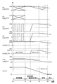
- FIG. 7 collectively describes the operations of the display device 100 according to the first embodiment described above.
- FIG. 7 shows temporal changes in the voltage applied to the pixel TFT2 and the switch TFT 92, the reference voltage Vref, and the power supply voltage Vpower.
- the scanning signal supplied from the gate driver 20 to each gate wiring 12 is set to the off voltage (VGL).
- VGL off-voltage
- the pixel TFT2 is turned off, the accumulated charge of the display pixel 1 is held. Therefore, the drain voltage VD (LCD_TFT) of the pixel TFT2 is held at the voltage level VLS corresponding to the accumulated charge.
- the charge accumulated in the display pixel 1 is discharged to a predetermined voltage (common signal voltage Vcom) via the pixel TFT2 and the source line 14. Is done.
- the drain voltage VD (LCD_TFT) of the pixel TFT2 decreases at a faster speed (corresponding to the line k3 in FIG. 6) than the natural discharge (corresponding to the line k1 in FIG. 6).
- the on-voltage can be supplied to the gate of the pixel TFT of each display pixel without going through the gate driver.
- the pixel TFT can be quickly turned on after the power is shut off, and the electric charge accumulated in each display pixel can be discharged.
- application of a DC voltage to the liquid crystal molecules can be prevented, deterioration of the display panel can be suppressed.
- the pixel TFTs of the respective display pixels can be simultaneously controlled to be on without using a gate driver, it is possible to easily construct the display device according to the first embodiment using a general-purpose gate driver. It becomes possible.
- the gate driver employs a configuration in which the scanning signal is supplied to the pixel TFT of each display pixel.
- the rise of the scanning signal at this time is determined by the operating speed of the gate driver. For this reason, the rising waveform of the scanning signal cannot be adjusted according to the state of the accumulated charge of each display pixel at the time when the power interruption occurs.
- rapid discharge cannot be performed, and there is a risk that suppression of afterimage generation will be insufficient.
- the display device can supply a scanning signal to the pixel TFT of each display pixel without using a gate driver, so that the rising waveform of the scanning signal at the time when the power-off is detected can be arbitrarily set. Can be adjusted.
- a display device capable of adjusting a rising waveform of a scanning signal will be described.
- FIG. 8 is a block diagram showing an embodiment of a liquid crystal display device to which the display device according to Embodiment 2 of the present invention is applied.
- liquid crystal display device 100A according to the second embodiment further includes power supply circuit 84 and switch 86, as compared with liquid crystal display device 100 according to the first embodiment shown in FIG.
- the power supply circuit 84 is electrically connected to the source wiring 96 and is configured to be able to control the drive voltage supplied to the source wiring 96 to an arbitrary voltage.
- the power supply monitoring circuit 70 divides the power supply voltage Vpower to generate a reference voltage Vref proportional to the power supply voltage Vpower.
- the power monitoring circuit 70 outputs the generated reference voltage Vref to the SW_TFT control signal generation unit 80 and the switch 86.
- the switch 86 is connected to the source wiring 96.
- the switch 86 is turned on / off according to the reference voltage Vref from the power supply monitoring circuit 70.
- the switch 86 is used as a representative example of an “opening / closing device” that can cut off the transmission path of the driving voltage to the source wiring 96.
- the switch 86 is turned on.
- a driving voltage is supplied from the power supply circuit 84 to the source wiring 96. This drive voltage is the source voltage VS (SW_TFT) of the switch TFT 92.
- the power supply circuit 84 can adjust the rising waveform of the drive voltage supplied to the source wiring 96.
- the power supply circuit 84 can adjust the rising speed of the drive voltage.
- the discharge rate of the accumulated charge in each display pixel increases.
- FIG. 9 shows temporal changes in the voltages applied to the pixel TFT2 and the switch TFT 92 in FIG.
- LCD_TFT also increases gradually. In other words, by slowing down the rising speed of the drive voltage, the discharge rate of the accumulated charge in each display pixel can be reduced.
- the discharge rate of the accumulated charges in the display pixel 1 can be controlled. Therefore, for example, when there is a possibility that a large current flows in the display panel 10 when the accumulated charges of the display pixels 1 are discharged all at once, the power supply circuit 84 slows the rising speed of the drive voltage. Therefore, it is possible to prevent the circuit and wiring in the display panel 10 from being damaged by a large current.
- the output waveform of the drive voltage supplied to the gate wiring via the switch TFT can be adjusted, so that it depends on the state of accumulated charge in the display pixel. Therefore, it is possible to appropriately discharge the accumulated charge.
- analog power supply generation unit 60 corresponds to an example of “power supply voltage generation unit” in the present invention
- power supply monitoring circuit 70 corresponds to “monitoring unit” in the present invention
- the switch TFT 92 corresponds to one embodiment of the “switch transistor” in the present invention
- the gate line 94 corresponds to an example of “first signal line” in the present invention
- the source line 96 corresponds to an example of “second signal line” in the present invention
- the power supply circuit 84 corresponds to the “power supply circuit” in the present invention.
- oxide semiconductor TFTs have higher field-effect mobility that indicates the ease of movement of evangelistic carriers in the active layer, so they can operate at higher speeds and have higher drive frequencies, resulting in higher definition. It is suitable for application to a drive device for a next-generation display device that is required.
- the oxide semiconductor film can be formed at room temperature and is in an amorphous state that does not include any crystal grain boundary, transistor characteristics (subthreshold value, current on / off (On / Off) between TFT elements). ) Ratio etc.) variation is small. Therefore, since a TFT having a uniform characteristic even in a large area can be manufactured, application as a driving switching TFT for a large area flat display is promising.
- the oxide semiconductor in addition to the above-described In—Ga—Zn—O system, a Zn—O system (ZnO), an In—Zn—O system (IZO), a Zn—Ti—O system (ZTO), and the like can be used. Preferably mentioned.
- the configuration in which the oxide semiconductor TFT is applied to the pixel TFT has a characteristic that the charge accumulated in the display pixel is less likely to be spontaneously discharged than the configuration in which the amorphous silicon TFT is applied.
- the field effect mobility of the oxide semiconductor TFT is about 10 cm 2 (Vs) ⁇ 1 or more, which is 10 times higher than that of the amorphous silicon TFT, and the on / off ratio is about 10 8 or more.
- the oxide semiconductor TFT is different from the amorphous silicon TFT in the threshold shift characteristic due to external stress (bias condition, temperature, etc.). Therefore, when an oxide semiconductor TFT is applied to a pixel TFT, it may be difficult to control a scanning signal (gate voltage) applied to the pixel TFT via a gate driver as in a conventional display device. There is.
- the scanning signal can be controlled without using a gate driver, and the output waveform of the scanning signal can be arbitrarily adjusted. Therefore, the effect of rapid discharge of accumulated charges can be exhibited.
- the switch TFT in the OFF state during normal driving.
- the on / off ratio of the oxide semiconductor TFT is as high as about 10 8 or more, it can be easily realized by applying the oxide semiconductor TFT to this switch TFT.
- the switch TFT is controlled to be in an off state during normal driving, and is controlled to be in an on state when the power is shut off.
- an oxide semiconductor TFT having a high field effect mobility to the switch TFT, effective switching can be performed.
Landscapes
- Physics & Mathematics (AREA)
- Engineering & Computer Science (AREA)
- General Physics & Mathematics (AREA)
- Chemical & Material Sciences (AREA)
- Crystallography & Structural Chemistry (AREA)
- Computer Hardware Design (AREA)
- Theoretical Computer Science (AREA)
- Nonlinear Science (AREA)
- Mathematical Physics (AREA)
- Optics & Photonics (AREA)
- Control Of Indicators Other Than Cathode Ray Tubes (AREA)
Abstract
アクティブマトリクス方式の表示装置において、電源遮断の発生時に各表示画素に蓄積された電荷を迅速に放電させること目的とする。 表示パネル(10)は、相互に直交して配設される複数のゲート配線(12)および複数のソース配線(14)の交点に対応して配置される複数の表示画素(1)を含む。アナログ電源生成部(60)は、電源(50)から供給される電源電圧(Vpower)を用いて、少なくとも表示画素を選択状態に設定する電圧レベルを有する駆動電圧(VGH)を生成してゲートドライバ(20)に供給する。電源監視回路(70)は、電源電圧を監視する。複数のスイッチTFT(92)は、複数のゲート配線およびアナログ電源生成部の間にそれぞれ設けられ、電源遮断が検出されたときにオンされることにより、アナログ電源生成部から各ゲート配線に駆動電圧を供給する。
Description
この発明は、表示装置に関し、より特定的には、電源遮断の発生時に各表示画素に蓄積された電荷を放電させるための技術に関する。
表示装置の一例として、液晶表示装置が知られている。液晶表示装置においては、複数の画素電極を薄膜トランジスタ(TFT:Thin Film Transistor)によってそれぞれ駆動する方式が広く採用されている。このような方式はアクティブマトリクス方式と呼ばれる。このようなアクティブマトリクス方式の液晶表示装置は、薄膜トランジスタに信号を供給するための基板上に配置されたゲート配線と、このゲート配線と交差するようにゲート配線より上側に配置された複数のソース配線とを備える。
たとえば特開2004-205588号公報(特許文献1)には、相互に直交して配設された複数のゲート配線および複数のソース配線の各交点近傍に複数の表示画素が2次元配列された表示パネルと、複数のゲート配線に走査信号を順次印加して、表示画素を所定のタイミングで選択状態に駆動するゲートドライバと、複数のソース配線の各々を介して、選択状態に設定された表示画素に表示信号電圧を印加するソースドライバとを備えた表示装置が開示される。
この特開2004-205588号公報(特許文献1)による表示装置は、所定の駆動電力に基づいて、少なくとも走査信号および表示信号電圧の電圧レベルを規定する複数の駆動電圧を生成して、ゲートドライバおよびソースドライバに供給する電源電圧供給回路をさらに備える。この電源電圧供給回路は、電源電池が脱落等することにより駆動電力の供給が遮断された場合には、接地電位を有する駆動電圧を生成してゲートドライバに供給する。これにより、表示パネルを構成する全ゲート配線に、接地電位を有する走査信号を供給して、全ての表示画素を選択状態に設定し、各表示画素に蓄積されていた電荷を所定電位(コモン信号電圧)に放電するように構成される。
上記の特許文献1に記載される表示装置において、電源電圧供給回路は、電源電池から正常に駆動電力が供給された表示駆動を実行している状態においては、駆動電圧として負電圧をゲートドライバに供給する一方で、電源電池からの駆動電力の遮断が検出された場合には、負電圧を有する駆動電圧を迅速に接地電位に移行させて、各表示画素に設けられた画素トランジスタ(画素TFT)をオンさせるように、ゲート配線に印加される走査信号の電圧レベルを制御する。これにより、各表示画素に蓄積された電荷を放電させ、電源遮断の発生に伴なって表示画像が徐々に消えていく残像の発生を抑制している。
ここで、TFTを画素トランジスタとする表示画素においては、一般的に、TFTの特性上、画素トランジスタに正電圧を有する走査信号を印加することによって画素トランジスタのターンオン動作を促進できる。しかしながら、上記の特許文献1に記載されるように、電源遮断が発生した場合においても、ゲートドライバからゲート配線に印加される走査信号の電圧レベルを制御する構成では、ゲートドライバの仕様により、制御可能な走査信号の電圧レベルが制約されてしまう。その結果、各表示画素に蓄積された電荷を迅速に放電させることが困難となっていた。
この発明はこのような問題点を解決するためになされたものであって、この発明の目的は、アクティブマトリクス方式の表示装置において、電源遮断の発生時に各表示画素に蓄積された電荷を迅速に放電させることである。
この発明のある局面では、表示装置は、相互に直交して配設される複数のゲート配線および複数のソース配線と、複数のゲート配線および複数のソース配線の交点に対応して配置される複数の表示画素とを含む表示パネルと、複数のゲート配線に走査信号を順次印加することにより、各表示画素を選択状態に設定するゲートドライバと、各ソース配線を介して、選択状態に設定された表示画素に表示信号電圧を印加するソースドライバと、電源から供給される電源電圧を用いて、少なくとも表示画素を選択状態に設定する電圧レベルを有する駆動電圧を生成してゲートドライバに供給する電源電圧生成部と、電源電圧を監視する監視部と、複数のゲート配線および電源電圧生成部の間にそれぞれ設けられ、監視部により電源の遮断が検出されたときにオンされることにより、各ゲート配線に対して電源電圧生成部からの駆動電圧を供給するように構成された複数のスイッチトランジスタとを備える。
この発明によれば、アクティブマトリクス方式の表示装置において、電源遮断の発生時に各表示画素に蓄積された電荷を迅速に放電させることができる。
以下、本発明の実施の形態について、図面を参照しながら詳細に説明する。なお、図中の同一または相当する部分には同一符号を付してその説明は繰返さない。
[実施の形態1]
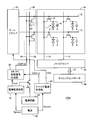
図1は、この発明の実施の形態1による表示装置を適用した液晶表示装置の一実施形態を示すブロック図である。
図1は、この発明の実施の形態1による表示装置を適用した液晶表示装置の一実施形態を示すブロック図である。
図1を参照して、液晶表示装置100は、複数の表示画素1が行列状に配列された表示パネル10と、ゲートドライバ20と、ソースドライバ30と、タイミングコントローラ40と、電源50と、アナログ電源生成部60とを備える。
表示パネル10は、対向する透明基板(図示せず)の間に互いに直交する方向に配設された複数のゲート配線12および複数のソース配線14と、複数のゲート配線12と複数のソース配線14との交点に対応して配置された複数の表示画素1とを含む。
各表示画素1は、画素電極4と、補助容量電極6と、薄膜トランジスタ(TFT)2とを含む。TFT2は、ドレイン電極が画素電極4に接続され、ソース電極がソース配線14に接続され、ゲート電極がゲート配線12に接続される。表示画素1は、画素電極4と画素電極4に対向して配置された共通電極(対向電極)との間に充填保持された液晶分子からなる液晶容量と、該液晶容量に並列に接続され、液晶容量に印加された信号電圧を保持するための蓄積容量とをさらに含む。
ゲートドライバ20は、表示パネル10の各行の表示画素群を順次走査して選択状態に設定する。ソースドライバ30は、選択状態に設定された行の表示画素群に、映像信号に基づく表示信号電圧を一括して出力する。具体的には、ゲートドライバ20は、複数のゲート配線12に走査信号(以下、「ゲートドライバ出力」とも称する。)を順次印加して各行の表示画素群を選択状態とする。ソースドライバ30は、各行の表示画素群が選択状態となるタイミングに同期して、表示信号電圧(以下、「ソースドライバ出力」とも称する。)を、各ソース配線14を介して各表示画素1に一斉に供給する。なお、このソースドライバ30における表示信号電圧の供給タイミングに同期して、該表示信号電圧に対して反転極性となるコモン信号電圧Vcomが対向電極に印加される。
タイミングコントローラ40は、装置外部から入力される映像信号に基づいて、ゲートドライバ20およびソースドライバ30の動作タイミングを制御する。なお、タイミングコントローラ40とソースドライバ30とは、一対の作動信号線によって構成されたデータ信号線32を介して接続される。このデータ信号線32を介してタイミングコントローラ40からソースドライバ30へ差動のデジタルのデータ信号が供給される。
上述した一連の動作を、1画面分の各行に対して繰り返し実行することにより、映像信号に基づく所望の画像情報が表示パネル10に表示される。なお、上述のように、TFT2は、画素電極4に表示信号電圧を供給するためのスイッチング素子(以下、「画素トランジスタ」とも称する。)として用いられるため、以下では、TFT2を「画素TFT(または、LCD_TFT)」とも表記する。
電源50は、接地電圧(0V)に負極側が接続された直流電源であり、ゲートドライバ20、ソースドライバ30およびアナログ電源生成部60に対して電源電圧Vpower(たとえば、3.3Vとする)を供給する。
アナログ電源生成部60は、電源50から供給される電源電圧Vpowerを用いて、表示パネル10の表示駆動に必要な駆動電圧を生成する。例えば、アナログ電源生成部60は、電源電圧Vpowerから駆動電圧VGHを生成してゲートドライバ20に供給する。ゲートドライバ20は、アナログ電源生成部60から供給される駆動電圧VGHに基づいて、走査信号のハイレベルを規定する電圧(オン電圧:正電圧)VGHと、走査信号のローレベルを規定する電圧(オフ電圧:負電圧)VGLとを生成する。
このように、表示装置100は、電源50から供給される電源電圧Vpowerに基づいて、上述した画像情報の表示駆動を行なっている。この表示駆動の途中で電源が遮断されると、電源50からゲートドライバ20、ソースドライバ30およびアナログ電源生成部60に供給される電源電圧Vpowerが接地電圧に移行する。そして、電源電圧Vpowerが接地電圧に移行することにより、アナログ電源生成部60からゲートドライバ20に供給される駆動電圧VGHも徐々に接地電圧に移行する。なお、駆動電圧VGHは、アナログ電源生成部60に設けられたコンデンサや負荷容量の自由放電に起因して、電源電圧Vpowerより遅い速度で接地電圧に至る。
ゲートドライバ20においては、電源遮断後、ゲート配線12に印加される走査信号がオフ電圧VGL(負電圧)に設定される。これにより、画素TFT2がオフ状態に制御されるため、画像情報を表示するために各表示画素(液晶容量、蓄積容量)に蓄積された電荷が保持されることになる。その結果、電源遮断後の比較的長い時間、表示パネル10の走査駆動が停止され、かつ、表示画素1に蓄積電荷が保持された状態となり、この蓄積電荷の放電に伴なって画像情報が徐々に消えていく残像が発生する。これにより、表示品質が悪化する。
また、各表示画素1に充填された液晶分子に直流電圧が印加されることになるため、液晶分子の劣化が進行し、ひいては表示パネル10の短命化を招くことになる。したがって、電源遮断が発生した場合には、各表示画素1に蓄積された電荷を迅速に放電させる必要がある。
本実施の形態1による表示装置100は、電源遮断後において各表示画素1の蓄積電荷を放電させるための構成として、表示パネル10と行方向に隣り合うように配置されたSW_TFTブロック90と、電源監視回路70と、SW_TFT制御信号生成部80とをさらに備える。
SW_TFTブロック90は、表示パネル10の列方向に配列された複数のTFT92と、複数のソース配線14と平行に配設されたゲート配線94およびソース配線96とを含む。
各TFT92は、各ゲート配線12とソース配線96との交点に配置される。TFT92は、ドレインがゲート配線12に接続され、ソースがソース配線96に接続され、ゲートがゲート配線94に接続される。TFT92は、表示画素1に含まれる画素TFT2と同一基板上に形成される。なお、TFT92は、画素TFT2と同一構造および同一プロセスで一体的に形成することができる。
ゲート配線94は、SW_TFT制御信号生成部80に接続される。ゲート配線94は、SW_TFT制御信号生成部80から供給される制御信号をTFT92のゲートに印加する。ソース配線96は、アナログ電源生成部60に接続される。図1に示すように、アナログ電源生成部60により生成された駆動電圧VGHは、ゲートドライバ20に供給されるとともに、ソース配線96に供給される。ソース配線96は、供給された駆動電圧VGHをTFT92のソースに印加する。
このような構成とすることにより、SW_TFT制御信号生成部80から供給される制御信号に応答してTFT92がオンされると、TFT92を介してソース配線96およびゲート配線12の間に電流経路が形成される。そして、この電流経路を通って、ソース配線96からゲート配線12に駆動電圧VGHが供給されることになる。
すなわち、SW_TFTブロック90に含まれる各TFT92は、制御信号に応答してオン状態となったときに、アナログ電源生成部60から出力される駆動電圧VGHをゲート配線12に伝達する。なお、駆動電圧VGHは、上述したように、表示駆動の実行中に、ゲートドライバ20から出力される走査信号のオン電圧(正電圧)に相当する。したがって、画素TFT2は、この駆動電圧VGH(オン電圧)を受けてオン状態に駆動される。
このように、TFT92は、ゲートドライバ20に代えて、ゲート配線12に供給される走査信号の信号レベルを制御するためのトランジスタ(以下、「スイッチトランジスタ」とも称する。)として用いられる。以下の説明では、画素TFT2と区別するために、TFT92を「スイッチTFT(または、SW_TFT)」とも表記する。
電源監視回路70は、電源50から供給される電源電圧Vpowerを検出する検出回路を含む。電源監視回路70は、電源電圧Vpowerの検出値に基づいて参照電圧Vrefを生成し、その生成した参照電圧VrefをSW_TFT制御信号生成部80へ出力する。なお、電源監視回路70により生成される参照電圧Vrefは、電源電圧Vpowerの電圧レベルに応じて可変に設定される。詳細には、電源電圧Vpowerの電圧レベルが低くなると、参照電圧Vrefは低く設定される。
SW_TFT制御信号生成部80は、アナログ電源生成部60から駆動電圧(VGH+α)を受け、電源監視回路70から参照電圧Vrefを受ける。なお、駆動電圧(VGH+α)は、後述するように、アナログ電源生成部60に含まれるチャージポンプ回路の出力電圧に相当する。SW_TFT制御信号生成部80は、チャージポンプ回路の出力電圧(=VGH+α)を用いて、スイッチTFT92のオンオフを制御する制御信号を生成する。
具体的には、SW_TFT制御信号生成部80は、参照電圧Vrefに応じて、駆動電圧(VGH+α)に等しい電圧を有する制御信号、および接地電圧(=0V)を有する制御信号のいずれか一方を生成する。SW_TFT制御信号生成部80により生成された制御信号は、ゲート配線94に供給される。すなわち、制御信号が有する電圧は、スイッチTFT92のゲート電圧(以下、「VG(SW_TFT)」とも記す。)となる。
図2を参照して、アナログ電源生成部60、電源監視回路70、およびSW_TFT制御信号生成部80についてさらに説明する。
アナログ電源生成部60は、DC/DCコンバータ62と、チャージポンプ回路64と、抵抗R1と、ツェナーダイオードZDとを含む。
DC/DCコンバータ62は、例えば昇圧チョッパ回路によって構成される。具体的には、DC/DCコンバータ62は、リアクトルL1と、トランジスタTr0と、ダイオードD0と、コンデンサC0と、抵抗R0とを含む。トランジスタTr0、コンデンサC0、および抵抗R0は、電源50を構成する直流電源の正極端子と負極端子との間に、並列に接続される。リアクトルL1は、直流電源の正極端子と、トランジスタTr0のコレクタとの間に接続される。ダイオードD0は、トランジスタTr0のコレクタとコンデンサC0の一方端との間に接続される。
DC/DCコンバータ62においては、図示しない制御部からのスイッチング指令に応答してトランジスタTr0がスイッチング動作することによって、電源電圧Vpowerが昇圧された電圧である電圧V2が生成される。より具体的には、トランジスタTr0のオン期間では電源電圧VpowerはリアクトルL1を通じて短絡され電流が流れるため、リアクトルL1の磁束レベルが上昇する。そして、トランジスタTr0のオフ期間では、リアクトルL1に電圧が発生し、その電圧が電源電圧Vpowerに加算されてダイオードD0が導通する。これにより、電圧V2を電源電圧Vpowerより上昇させる。この電圧V2は、リアクトルL1およびダイオードD0の接続ノードの電圧V1とともに、チャージポンプ回路64に供給される。
チャージポンプ回路64は、コンデンサC1,C2,C3と、ダイオードD1,D2とを含む。コンデンサC1の一方端は、リアクトルL1およびダイオードD0の接続ノードに接続され、他方端はダイオードD1の陽極(アノード)およびダイオードD2の陰極(カソード)に接続される。コンデンサC2の一方端はダイオードD1のカソードに接続され、他方端はダイオードD2のアノードに接続される。コンデンサC3の一方端はダイオードD2のアノードに接続され、他方端はDC/DCコンバータ62のダイオードD0のカソードに接続される。
チャージポンプ回路64は、コンデンサC1の一方端に電圧V1を受け、コンデンサC3の他方端に電圧V2を受ける。チャージポンプ回路64は、トランジスタTr0のスイッチング動作に応じて矩形波状に変化する電圧V1と、電圧V2との差に応じて充電動作および放電動作を繰り返し実行することにより、駆動電圧VGHより所定電圧α上回る電圧(=VGH+α)を生成する。チャージポンプ回路64は、その生成した駆動電圧(VGH+α)を出力線66に出力する。
駆動電圧(VGH+α)が与えられる出力線66と、接地電圧(0V)が与えられる接地ノード8との間には、抵抗R1およびツェナーダイオードZDからなる直列回路が接続される。ツェナーダイオードZDは、カソードが抵抗R1に接続され、アノードが接地ノード8に接続される。抵抗R1およびツェナーダイオードZDの接続ノード(図中のノードN1に相当)は、アナログ電源生成部60の出力ノードを構成する。なお、図示は省略するが、この出力ノードN1は、ゲートドライバ20およびソース配線96(図1)と電気的に接続されている。
出力線66に印加される駆動電圧(VGH+α)が大きくなると、ツェナーダイオードZDに加わる逆方向電圧が増加する。そして、逆方向電圧が降伏電圧を超えると、ツェナーダイオードZDのカソードからアノードへ流れる電流(逆方向電流)が急激に増加する。降伏現象が起きると、ツェナーダイオードZDの電圧は、逆方向電流の大きさとは無関係に一定値(降伏電圧)をとる。
本実施の形態1では、ツェナーダイオードZDは、駆動電圧VGHを降伏電圧とする。したがって、ツェナーダイオードZDの電圧は、逆方向電流が変化してもほとんど一定(駆動電圧VGH)となる。これにより、アナログ電源生成部60の出力ノードN1には、定電圧(駆動電圧VGH)が出力される。ゲートドライバ20は、この駆動電圧VGHに基づいて走査信号のオン電圧を生成する。すなわち、駆動電圧VGHは、画素TFT2のゲート電圧(以下、「VG(LCD_TFT)」とも記す。)となる。さらに、駆動電圧VGHは、ソース配線96に供給されることによってスイッチTFT92のソース電圧(以下、「VS(SW_TFT)」とも記す。)となる。
さらに、チャージポンプ回路64の出力線66には、SW_TFT制御信号生成部80が接続される。SW_TFT制御信号生成部80は、出力線66と接地ノード8との間に直列に接続された抵抗R4およびトランジスタTr1を含む。トランジスタTr1は、コレクタが抵抗R4に接続され、エミッタが接地ノード8に接続され、かつ、ベースが電源監視回路70の出力ノード(図中のノードN3に相当)に接続される。抵抗R4およびトランジスタTr1の接続ノード(図中のノードN2に相当)は、SW_TFT制御信号生成部80の出力ノードを構成する。
電源監視回路70は、電源50から電源電圧Vpowerを受ける電源ノード9と接地ノード8との間に直列に接続された抵抗R2,R3を含む。抵抗R2およびR3の接続ノードN3は、電源監視回路70の出力ノードを構成する。電源監視回路70は、電源電圧Vpowerを分圧し、電源電圧Vpowerに比例した参照電圧Vrefを生成する。電源監視回路70により生成された参照電圧Vrefは、出力ノードN3を介してSW_TFT制御信号生成部80のトランジスタTr1のベースに入力される。これにより、トランジスタTr1のベース-エミッタ間電圧VBEは参照電圧Vrefと等しくなる(VBE=Vref)。
ここで、トランジスタTr1がオンするときのベース-エミッタ間電圧VBEをVf(たとえば、0.7Vとする)とすると、参照電圧VrefがVf(=0.7V)より高いときには(Vref>Vf)、トランジスタTr1がオンされる。トランジスタTr1がオンされることにより、出力ノードN2からは接地電圧を有する制御信号が出力される。
これに対して、参照電圧VrefがVf(=0.7V)以下であるときには(Vref≦Vf)、トランジスタTr1がオンされないため、出力ノードN2からは駆動電圧(VGH+α)に等しい電圧を有する制御信号が出力される。
なお、電源監視回路70において、参照電圧Vrefは、抵抗R2,R3の抵抗値を調整することによって可変に設定することができる。本実施の形態1では、電源電圧Vpowerに対して判定値Vpower_thが設定される。この判定値Vpower_thは、電源が遮断されたか否かを判別するための閾値(たとえば、2.7Vとする)である。電源監視回路70は、電源電圧Vpowerと判定値Vpower_thとを比較し、その比較結果に基づいて電源遮断を検出する。抵抗R2,R3の抵抗値は、判定値Vpower_thを分圧して生成される参照電圧VrefがVf(=0.7V)と等しくなるように設定される。これにより、電源電圧Vpowerが判定値Vpower_thより高いとき、すなわち、電源50から正常に電力が供給されている通常駆動時には、参照電圧VrefがVfより高くなるため、トランジスタTr1がオンされ、SW_TFT制御信号生成部80の出力ノードN2から接地電圧を有する制御信号が出力される。
そして、電源遮断の発生によって電源電圧Vpowerが低下し、判定値Vpower_thに到達すると、参照電圧Vref=Vfとなるため、トランジスタTr1がオフされる。よって、出力ノードN2からは駆動電圧(VGH+α)に等しい電圧を有する制御信号が出力される。
このように、SW_TFT制御信号生成部80は、アナログ電源生成部60により生成される駆動電圧(VGH+α)を用いて、スイッチTFT92のオンオフを制御する制御信号を生成してゲート配線94に出力する。この制御信号(=VG(SW_TFT))は、電源電圧Vpowerが判定値Vpower_thより高いとき(すなわち、通常駆動時)に接地電圧を有する一方で、電源電圧Vpowerが判定値Vpower_th以下のとき(すなわち、電源遮断時)に駆動電圧(VGH+α)に等しい電圧を有する。
図3および図4を用いて、通常駆動時および電源遮断時におけるスイッチTFT92および表示画素1の動作を詳細に説明する。
図3には、本実施の形態1による表示装置のうちの表示パネル10およびSW_TFTブロック90が抽出して示されている。なお、図3では、表示パネル10において1個の表示画素1が代表して示され、かつ、SW_TFTブロック90において1個のスイッチTFT92が代表して示されている。
図3を参照して、通常駆動時には、ゲートドライバ20(図1)からゲート配線12に印加される走査信号(ゲートドライバ出力)に応答して表示画素1が選択状態となるタイミングに同期して、表示信号電圧(ソースドライバ出力)がソース配線14を介して表示画素1に印加される。また、ソースドライバ出力の印加タイミングに同期して、表示信号電圧に対して反転極性となるコモン信号電圧Vcomが対向電極に印加される。
このような表示駆動の実行中、SW_TFTブロック90においては、アナログ電源生成部60からソース配線96に対して駆動電圧VGHが供給される(すなわち、VS(SW_TFT)=VGH)。また、SW_TFT制御信号生成部80からゲート配線94に対して接地電圧を有する制御信号が供給される(すなわち、VG(SW_TFT)=0V)。この制御信号に応答してスイッチTFT92がオフ状態となるため、ソース配線96およびゲート配線12の間の電流経路が遮断される。したがって、駆動電圧VGHはゲート配線12に伝達されない。
これに対して、表示駆動の実行中に電源遮断が発生した場合には、ゲートドライバ20に供給される電源電圧Vpowerおよび駆動電圧VGHが接地電圧に移行する。ゲートドライバ出力は駆動電圧VGLに設定される。駆動電圧VGLは走査信号のオフ電圧(負電圧)に相当するため、画素TFT2はオフ状態に制御される。そのため、各表示画素1に蓄積された電荷が保持された状態となる。
図4は、画素TFT2およびスイッチTFT92に印加される電圧の時間的な変化を示す図である。電源遮断が発生した時点(時刻t1)から電源電圧Vpowerが低下し始め、その後の時刻t2で電源電圧Vpowerが判定値Vpower_thに到達すると、SW_TFT制御信号生成部80からゲート配線94に対して駆動電圧(VGH+α)に等しい電圧を有する制御信号が供給される。これにより、SW_TFTブロック90においては、スイッチTFT92のゲート電圧VG(SW_TFT)が接地電圧から駆動電圧(VGH+α)に変化する。なお、ソース配線96には、アナログ電源生成部60からの駆動電圧VGHが供給されている(VS(SW_TFT)=VGH)。
そして、時刻t2において、制御信号(=VG(SW_TFT))の立上りに応答してスイッチTFT92がオンされると、スイッチTFT92を介してソース配線96およびゲート配線12の間に電流経路が形成される。この電流経路を通って、ソース配線96からゲート配線12に駆動電圧VGHが供給される。これにより、画素TFT2のゲート電圧VG(LCD_TFT)は、駆動電圧VGL(オフ電圧)から駆動電圧VGH(オン電圧)に変化する。
なお、SW_TFTブロック90では、ゲート配線94に接続される複数のスイッチTFT92が制御信号(=VG(SW_TFT))の立上りに応答して同時にオンされるため、表示パネル10内の複数のゲート配線12には一斉に駆動電圧VGH(オン電圧)が供給される。各ゲート配線12を介して各画素TFT2のゲートに駆動電圧VGH(オン電圧)が印加されることにより、全ての画素TFT2が一斉にオンされる。これにより、各表示画素1に蓄積された電荷が画素TFT2およびソース配線14を介して、所定電圧(コモン信号電圧Vcom)に放電される。
このように、本実施の形態1による表示装置では、電源遮断を検出してオン状態に駆動されるスイッチTFT92を介して、アナログ電源生成部60からゲート配線12に対して駆動電圧VGH(オン電圧)を供給する。すなわち、電源遮断が発生した場合には、ゲートドライバ20を介さずに駆動電圧VGH(オン電圧)をゲート配線12に供給することができる点で、従来の表示装置と相違する。
以下では、本実施の形態1による表示装置と従来の表示装置との相違点について、図面を参照して詳細に説明する。
図5および図6は、従来の表示装置における電源遮断時の表示画素1の動作を説明する図である。図5には、従来の表示装置のうちの表示パネル10を抽出して示す。図5では、1個の表示画素1が代表して示されている。図6には、図5の画素TFT2に印加される電圧の時間的な変化を示す。
なお、従来の表示装置において表示パネル10の構成は、図1と同様の構成であるので詳細な説明は繰り返さない。また、通常駆動時の表示画素1の動作についても、本実施の形態1におけるそれと同じであるので、詳細な説明を繰り返さない。
従来の表示装置においては、電源遮断が発生すると(時刻t1)、ゲートドライバ(図示せず)から各ゲート配線12に供給される走査信号はオフ電圧(VGL)に設定される。オフ電圧VGLをゲートに受けて画素TFT2がオフすると、表示画素1の蓄積電荷が保持された状態となる。そのため、画素TFT2のドレイン電圧(以下、「VD(LCD_TFT)」とも記す。)は、蓄積電荷に応じた電圧レベルVLSに保持される。また、画素TFT2のソース電圧VS(LCD_TFT)は、接地電圧となる。なお、電源遮断後における蓄積電荷の自然放電によって、ドレイン電圧VD(LCD_TFT)は電圧VLSから徐々に低下する(図6中のラインk1に相当)。
電源から供給される電源電圧に基づいて、ゲートドライバおよびソースドライバに供給する駆動電圧を生成する電源電圧供給回路(図示せず)は、電源遮断を検出すると(時刻t2)、ゲートドライバに供給する駆動電圧を接地電圧以上となるように制御する。これにより、ゲートドライバから各ゲート配線12を介して各表示画素1の画素TFT2のゲートに印加される走査信号(=VG(LCD_TFT))の電圧レベルは、接地電圧以上に上昇する。走査信号の電圧レベルが上昇したことによって画素TFT2がオンすると、各表示画素1に蓄積された電荷が画素TFT2、ソース配線14を介してコモン信号電圧Vcomに放電される。画素TFT2のドレイン電圧VD(LCD_TFT)は、自然放電よりも速い速度で低下する(図6中のラインk2に相当)。
このように、従来の表示装置では、電源遮断が発生すると、ゲートドライバを介して接地電圧以上の電圧を有する走査信号をゲート配線12に供給することにより、画素TFT2をオン状態に駆動する。したがって、ゲートドライバは、電源が遮断された状態においても、所望の電圧をゲート配線12に供給するための動作を行なう必要がある。
しかしながら、表示装置に汎用されるゲートドライバは、電源からの電力供給が遮断された状態においては走査信号の電圧レベルを制御することができない。よって、上述した動作を実現するためには、専用のゲートドライバを設ける必要が生じる。
さらに、汎用的なゲートドライバは、シフトレジスタを搭載しており、該シフトレジスタから複数のゲート配線12に走査信号を順次印加して各行の表示画素群を選択状態とするように構成されているため、複数のゲート配線12に一斉に走査信号を印加することができない。そのため、蓄積電荷の放電の迅速性についてはある程度限界がある。
また、ゲートドライバが複数のゲート配線12に一斉に走査信号を印加する機能を備えている場合であっても、複数のゲート配線12に走査信号を印加する際には通常駆動時に流れる電流の数百倍の電流がゲートドライバに流れることになるため、大電流に耐え得るようにゲートドライバの回路規模や配線スペース等を設計する必要が生じる。
さらに、汎用的なゲートドライバにおいて、オフ電圧VGL(負電圧)を出力する回路部から接地電圧以上の電圧を出力させることは、ゲートドライバに内蔵される保護回路の破壊に繋がる虞がある。したがって、保護回路を破壊させないための対策回路をゲートドライバに搭載する必要が生じる。
これに対して、図3および図4に示したように、本実施の形態1による表示装置においては、電源が遮断した場合には、ゲートドライバ20に代えて、SW_TFTブロック90内の各スイッチTFT92が各ゲート配線12にオン電圧(VGH)を供給することから、上述したゲートドライバにおける問題を回避することができる。
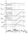
図7は、以上説明した、本実施の形態1による表示装置100の動作をまとめて記載したものである。図7には、画素TFT2およびスイッチTFT92に印加される電圧、参照電圧Vref、および電源電圧Vpowerの時間的な変化を示す。
図7を参照して、電源遮断が発生すると(時刻t1)、ゲートドライバ20から各ゲート配線12に供給される走査信号はオフ電圧(VGL)に設定される。オフ電圧(VGL)をゲートに受けて画素TFT2がオフすると、表示画素1の蓄積電荷が保持された状態となる。そのため、画素TFT2のドレイン電圧VD(LCD_TFT)は、蓄積電荷に応じた電圧レベルVLSに保持される。
電源遮断が発生した時点(時刻t1)から電源電圧Vpowerが低下し始め、その後の時刻t2において判定値Vpower_thに到達すると、電源監視回路70により生成される参照電圧Vref(=トランジスタTr1のベース-エミッタ間電圧VBE)がVf(=0.7V)に到達する。この参照電圧Vref(=Vf)をゲートに受けてトランジスタTr1がオンすることにより、SW_TFT制御信号生成部80からゲート配線94に供給される制御信号の電圧レベル(=VG(SW_TFT))は、接地電圧から駆動電圧(VGH+α)に変化する。なお、ソース配線96には、アナログ電源生成部60からの駆動電圧VGHが供給されている(VS(SW_TFT)=VGH)。
制御信号(=VG(SW_TFT))の立上りに応答してスイッチTFT92がオンされると、スイッチTFT92を介してソース配線96からゲート配線12に駆動電圧VGHが伝達される。これにより、画素TFT2のゲート電圧VG(LCD_TFT)は、オフ電圧(VGL)からオン電圧(VGH)に変化する。
オン電圧(VGH)をゲートに受けて画素TFT2がオン状態に駆動されると、表示画素1に蓄積された電荷が画素TFT2およびソース配線14を介して、所定電圧(コモン信号電圧Vcom)に放電される。画素TFT2のドレイン電圧VD(LCD_TFT)は、自然放電(図6中のラインk1に相当)よりも速い速度で低下する(図6中のラインk3に相当)。
ここで、従来の表示装置と本実施の形態1による表示装置との間で、表示画素1の蓄積電荷の放電速度を比較すると、従来の表示装置では、電源遮断後における走査信号(=VG(LCD_TFT))の立上り速度がゲートドライバの動作速度等に依存するため、蓄積電荷の放電速度の向上には自ずと限界がある。これに対して、本実施の形態1による表示装置では、電源遮断後における走査信号(=VG(LCD_TFT))の立上り速度はスイッチTFT92のオン特性に主に依存しているため、蓄積電荷の放電速度をより高めることができる。
このように、本実施の形態1による表示装置によれば、電源遮断時には、ゲートドライバを介さずに各表示画素の画素TFTのゲートにオン電圧を供給することができる。これにより、電源遮断後に迅速に画素TFTをオンさせて、各表示画素に蓄積された電荷を放電することができる。この結果、電源遮断の発生に伴なって表示画素が徐々に消えていく残像の発生を抑制できるため、表示品質を向上できる。また、液晶分子への直流電圧の印加を防止できるので、表示パネルの劣化を抑制できる。
さらには、ゲートドライバを介さずに各表示画素の画素TFTを同時にオン状態に制御することができることから、汎用的なゲートドライバを用いて本実施の形態1による表示装置を簡易に構築することが可能となる。
[実施の形態2]
実施の形態1で説明したように、従来の表示装置では、電源遮断が発生した場合にも、ゲートドライバが各表示画素の画素TFTに走査信号を供給する構成を採用するため、電源遮断を検出した時点における走査信号の立上りが、ゲートドライバの動作速度等によって決まってしまう。そのため、電源遮断が発生した時点における各表示画素の蓄積電荷の状態に応じて走査信号の立上り波形を調整することができない。この結果、蓄積電荷の状態によっては、迅速な放電を行なうことができず、残像の発生の抑制が不十分となってしまう虞がある。
実施の形態1で説明したように、従来の表示装置では、電源遮断が発生した場合にも、ゲートドライバが各表示画素の画素TFTに走査信号を供給する構成を採用するため、電源遮断を検出した時点における走査信号の立上りが、ゲートドライバの動作速度等によって決まってしまう。そのため、電源遮断が発生した時点における各表示画素の蓄積電荷の状態に応じて走査信号の立上り波形を調整することができない。この結果、蓄積電荷の状態によっては、迅速な放電を行なうことができず、残像の発生の抑制が不十分となってしまう虞がある。
一方、本実施の形態1による表示装置は、ゲートドライバを介さずに各表示画素の画素TFTに走査信号を供給することができるため、電源遮断を検出した時点における走査信号の立上り波形を任意に調整することができる。実施の形態2では、走査信号の立上り波形を調整することが可能な表示装置を説明する。
図8は、この発明の実施の形態2による表示装置を適用した液晶表示装置の一実施形態を示すブロック図である。
図8を参照して、実施の形態2による液晶表示装置100Aは、図1に示した実施の形態1による液晶表示装置100と比較して、電源回路84と、スイッチ86とをさらに備える。
電源回路84は、ソース配線96と電気的に接続されており、ソース配線96に供給する駆動電圧を任意の電圧に制御可能に構成される。
電源監視回路70は、電源電圧Vpowerを分圧し、電源電圧Vpowerに比例した参照電圧Vrefを生成する。電源監視回路70は、生成した参照電圧VrefをSW_TFT制御信号生成部80およびスイッチ86へ出力する。
スイッチ86は、ソース配線96に介挿接続される。スイッチ86は、電源監視回路70からの参照電圧Vrefに応じてオンオフされる。なお、スイッチ86は、ソース配線96への駆動電圧の伝達経路を遮断可能な「開閉装置」の代表例として用いられる。
具体的には、スイッチ86は、参照電圧VrefがVf(=0.7V)より高いとき(Vref>Vf)、オフ状態とされる。したがって、ソース配線96には駆動電圧が供給されない。一方、参照電圧VrefがVf(=0.7V)以下であるとき(Vref≦Vf)、スイッチ86はオンされる。スイッチ86がオンされることにより、電源回路84からソース配線96に駆動電圧が供給される。この駆動電圧は、スイッチTFT92のソース電圧VS(SW_TFT)となる。
電源回路84は、ソース配線96に供給する駆動電圧の立上り波形を調整することができる。例えば、電源回路84は、駆動電圧の立上り速度を調整することができる。電源回路84が駆動電圧の立上り速度を速くした場合には、電源遮断が検出された時点でスイッチ86がオンすると、電源回路84からソース配線96に供給される駆動電圧(=VS(SW_TFT))が急峻に増加する。これにより、スイッチTFT92を介してソース配線96からゲート配線12に供給される駆動電圧(=VG(LCD_TFT))も急峻に増加する。この結果、各表示画素における蓄積電荷の放電速度が上昇する。
その一方で、電源回路84が駆動電圧の立上り速度を遅くした場合には、電源遮断が検出された時点でスイッチ86がオンすると、電源回路84からソース配線96に供給される駆動電圧(=VS(SW_TFT))が緩やかに増加する。図9には、図8の画素TFT2およびスイッチTFT92に印加される電圧の時間的な変化を示す。図9を参照して、ソース配線96に供給される駆動電圧(=VS(SW_TFT))が緩やかに増加すると、スイッチTFT92を介してソース配線96からゲート配線12に供給される駆動電圧(=VG(LCD_TFT))も緩やかに増加する。すなわち、駆動電圧の立上り速度を遅くすることによって、各表示画素における蓄積電荷の放電速度を低下させることができる。
このように、電源回路84から任意の波形を有する駆動電圧をソース配線96に供給可能な構成としたことにより、表示画素1における蓄積電荷の放電速度を制御することが可能となる。したがって、例えば、各表示画素1の蓄積電荷を一斉に放電させたときに表示パネル10内に大電流が流れる可能性がある場合には、電源回路84が駆動電圧の立上り速度を遅くすることにより、大電流によって表示パネル10内の回路および配線等が損傷するのを防止することができる。
このように、本実施の形態2による表示装置によれば、スイッチTFTを介してゲート配線に供給される駆動電圧の出力波形を調整することができるため、表示画素における蓄積電荷の状態に応じて、蓄積電荷の放電を適切に実行することが可能となる。
なお、上記の実施の形態1および2において、アナログ電源生成部60は、この発明における「電源電圧生成部」の一実施例に対応し、電源監視回路70は、この発明における「監視部」の一実施例に対応し、スイッチTFT92は、この発明における「スイッチトランジスタ」の一実施例に対応する。また、ゲート配線94は、この発明における「第1の信号線」の一実施例に対応し、ソース配線96は、この発明における「第2の信号線」の一実施例に対応する。また、電源回路84は、この発明における「電源回路」に対応する。
(画素TFTおよびスイッチTFTの構成例)
上述した実施の形態1および2では、画素トランジスタおよびスイッチトランジスタの各々にTFTを適用する構成について説明した。このTFTにおいては、従来より、半導体チャネル層(活性層)としてシリコン半導体やその化合物が多く用いられており、特にディスプレイ用途等大面積化への対応が要求される液晶駆動装置用にはアモルファスシリコンが用いられていた。
上述した実施の形態1および2では、画素トランジスタおよびスイッチトランジスタの各々にTFTを適用する構成について説明した。このTFTにおいては、従来より、半導体チャネル層(活性層)としてシリコン半導体やその化合物が多く用いられており、特にディスプレイ用途等大面積化への対応が要求される液晶駆動装置用にはアモルファスシリコンが用いられていた。
近年では、このアモルファスシリコンに代えて、In-Ga-Zn-O系の酸化物半導体を活性層に用いたTFTが提案されている。このような酸化物半導体を活性層としたTFTは、「酸化物半導体TFT」とも称される。酸化物半導体TFTは、アモルファスシリコンTFTと比較して、活性層中の伝道キャリアの動き易さを示す電界効果移動度が高いため、高速で動作でき、かつ、駆動周波数も高いため、高精細化を求められる次世代表示装置の駆動装置への応用に好適である。
また、酸化物半導体膜は、室温にて成膜可能であり、結晶粒界を一切含まないアモルファス状態であることから、TFT素子間のトランジスタ特性(サブスレショルド値、電流オン・オフ(On/Off)比など)のばらつきが少ない。したがって、大面積でも特性が均一なTFTを作製できるため、大面積平面ディスプレイ用の駆動スイッチングTFTとしての適用が有望視されている。なお、酸化物半導体としては、上述したIn-Ga-Zn-O系の他、Zn-O系(ZnO)、In-Zn-O系(IZO)、Zn-Ti-O系(ZTO)などが好適に挙げられる。
上述した実施の形態1および2において、このような酸化物半導体TFTを、画素TFTおよびスイッチTFTに適用することによって、蓄積電荷の迅速な放電という本発明の効果を高めることが可能となる。
詳細には、画素TFTに酸化物半導体TFTを適用する構成では、アモルファスシリコンTFTを適用した構成と比較して、表示画素に蓄積された電荷が自然放電しにくいという特性を有する。これは、酸化物半導体TFTの電界効果移動度が約10cm2(Vs)-1以上とアモルファスシリコンTFTの10倍以上も高いこと、および、On/Off比が約108以上という優れたトランジスタ特性を示すことによる。本実施の形態1および2による表示装置では、電源遮断の発生時に画素トランジスタに対してしきい値以上のゲート電圧(オン電圧VGH)を印加する。このゲート電圧を受けて酸化物半導体TFTがオンすることによって蓄積電荷の積極的な放電を促すこととなるため、アモルファスシリコンTFTと比較して、迅速な放電に大きな効果が期待できる。
また、酸化物半導体TFTは、外部ストレス(バイアス条件および温度等)によるしきい値のシフト特性がアモルファスシリコンTFTとは異なっている。そのため、酸化物半導体TFTを画素TFTに適用した場合には、従来の表示装置のように、ゲートドライバを介して画素TFTに印加する走査信号(ゲート電圧)を制御することが困難となる可能性がある。本実施の形態1および2では、ゲートドライバを介さずに走査信号を制御でき、かつ、走査信号の出力波形を任意に調整できることから、蓄積電荷の迅速な放電という効果を発揮することができる。
さらに、本実施の形態1および2においては、通常駆動時にはスイッチTFTをオフ状態に維持することが望ましい。上述したように、酸化物半導体TFTはOn/Off比が約108以上と高いことから、このスイッチTFTに酸化物半導体TFTを適用することによって容易に実現することができる。
また、本実施の形態1および2では、スイッチTFTは、通常駆動時にオフ状態に制御される一方で、電源遮断時にはオン状態に制御される。このスイッチTFTに、高い電界効果移動度を有する酸化物半導体TFTを適用することにより、効果的なスイッチングが可能となる。
今回開示された実施の形態は、すべての点で例示であって制限的なものではないと考えられるべきである。本発明の範囲は、上記した実施の形態の説明ではなくて請求の範囲によって示され、請求の範囲と均等の意味および範囲内でのすべての変更が含まれることが意図される。
1 表示画素、2 画素TFT、4 画素電極、6 補助容量電極、10 表示パネル、12,94 ゲート配線、14,96 ソース0配線、20 ゲートドライバ、30 ソースドライバ、32 データ信号線、40 タイミングコントローラ、50 電源、60 アナログ電源生成部、62 DC/DCコンバータ、64 チャージポンプ回路、66 出力線、70 電源監視回路、80 SW_TFT制御信号生成部、84 電源回路、86 スイッチ、90 SW_TFTブロック、92 スイッチTFT、100,100A 表示装置。
Claims (8)
- 相互に直交して配設される複数のゲート配線および複数のソース配線と、前記複数のゲート配線および前記複数のソース配線の交点に対応して配置される複数の表示画素とを含む表示パネルと、
前記複数のゲート配線に走査信号を順次印加することにより、各前記表示画素を選択状態に設定するゲートドライバと、
各前記ソース配線を介して、前記選択状態に設定された前記表示画素に表示信号電圧を印加するソースドライバと、
電源から供給される電源電圧を用いて、少なくとも前記表示画素を選択状態に設定する電圧レベルを有する駆動電圧を生成して前記ゲートドライバに供給する電源電圧生成部と、
前記電源電圧を監視する監視部と、
前記複数のゲート配線および前記電源電圧生成部の間にそれぞれ設けられ、前記監視部により前記電源の遮断が検出されたときにオンされることにより、各前記ゲート配線に対して前記電源電圧生成部からの前記駆動電圧を供給するように構成された複数のスイッチトランジスタとを備える、表示装置。 - 前記監視部により前記電源の遮断が検出されたときに、前記複数のスイッチトランジスタをオンするための制御信号を出力する制御信号生成部をさらに備える、請求項1に記載の表示装置。
- 前記複数のソース配線と平行に配設され、前記制御信号を各前記スイッチトランジスタのゲートに印加するための第1の信号線と、
前記複数のソース配線と平行に配設され、前記駆動電圧を各前記スイッチトランジスタのソースに印加するための第2の信号線とをさらに備え、
前記複数のスイッチトランジスタは、前記複数のゲート配線と前記第1および第2の信号線との交点に対応して配置され、かつ、ドレインが前記複数のゲート配線にそれぞれ接続される、請求項2に記載の表示装置。 - 前記電源電圧生成部は、前記電源電圧を用いて前記表示画素を選択状態に設定する電圧レベルを有する駆動電圧を生成可能に構成されたチャージポンプ回路を含み、
前記制御信号生成部は、前記監視部により前記電源の遮断が検出されたときに、前記チャージポンプ回路からの前記駆動電圧を、前記制御信号として前記第1の信号線に出力するように構成される、請求項3に記載の表示装置。 - 前記監視部により前記電源の遮断が検出されたときに、前記複数のスイッチトランジスタをオンするための制御信号を出力する制御信号生成部と、
オン状態の各前記スイッチトランジスタを介して各前記ゲート配線に供給される前記駆動電圧の出力波形を調整可能に構成された電源回路とをさらに備える、請求項1に記載の表示装置。 - 前記複数のソース配線と平行に配設され、前記制御信号を各前記スイッチトランジスタのゲートに印加するための第1の信号線と、
前記複数のソース配線と平行に配設され、前記電源回路からの前記駆動電圧を各前記スイッチトランジスタのソースに印加するための第2の信号線とをさらに備え、
前記複数のスイッチトランジスタは、前記複数のゲート配線と前記第1および第2の信号線との交点に対応して配置され、かつ、ドレインが前記複数のゲート配線にそれぞれ接続される、請求項5に記載の表示装置。 - 前記表示画素は、前記ゲート配線および前記ソース配線の交点に配置された画素トランジスタを含み、
前記画素トランジスタおよび前記スイッチトランジスタは、酸化物半導体薄膜トランジスタからなり、同一基板上に形成される、請求項1から6のいずれか1項に記載の表示装置。 - 表示装置の駆動方法であって、
前記表示装置は、
相互に直交して配設される複数のゲート配線および複数のソース配線と、前記複数のゲート配線および前記複数のソース配線の交点に対応して配置される複数の表示画素とを有する表示パネルと、
前記複数のゲート配線に走査信号を順次印加することにより、各前記表示画素を選択状態に設定するゲートドライバと、
前記複数のソース配線の各々を介して、前記選択状態に設定された前記表示画素に表示信号電圧を印加するソースドライバと、
電源から供給される電源電圧を用いて、少なくとも前記表示画素を選択状態に設定する電圧レベルを有する駆動電圧を生成して前記ゲートドライバに供給する電源電圧生成部と、
前記複数のゲート配線および前記電源電圧生成部の間にそれぞれ設けられる複数のスイッチトランジスタとを含み、
前記駆動方法は、
前記電源電圧を監視するステップと、
前記監視するステップにより前記電源の遮断が検出されたときに各前記スイッチトランジスタをオンすることにより、各前記ゲート配線に対して前記電源電圧生成部からの前記駆動電圧を供給するステップとを備える、表示装置の駆動方法。
Applications Claiming Priority (2)
| Application Number | Priority Date | Filing Date | Title |
|---|---|---|---|
| JP2012127979 | 2012-06-05 | ||
| JP2012-127979 | 2012-06-05 |
Publications (1)
| Publication Number | Publication Date |
|---|---|
| WO2013183531A1 true WO2013183531A1 (ja) | 2013-12-12 |
Family
ID=49711923
Family Applications (1)
| Application Number | Title | Priority Date | Filing Date |
|---|---|---|---|
| PCT/JP2013/064998 Ceased WO2013183531A1 (ja) | 2012-06-05 | 2013-05-30 | 表示装置およびその駆動方法 |
Country Status (1)
| Country | Link |
|---|---|
| WO (1) | WO2013183531A1 (ja) |
Cited By (4)
| Publication number | Priority date | Publication date | Assignee | Title |
|---|---|---|---|---|
| CN105301859A (zh) * | 2015-11-25 | 2016-02-03 | 昆山龙腾光电有限公司 | 阵列基板和液晶显示装置 |
| CN108281118A (zh) * | 2018-01-09 | 2018-07-13 | 昆山龙腾光电有限公司 | 显示面板及液晶显示装置 |
| CN109410878A (zh) * | 2018-12-18 | 2019-03-01 | 惠科股份有限公司 | 一种驱动电路、驱动装置以及显示装置 |
| WO2020124703A1 (zh) * | 2018-12-18 | 2020-06-25 | 惠科股份有限公司 | 一种驱动电路、驱动装置及显示装置 |
Citations (3)
| Publication number | Priority date | Publication date | Assignee | Title |
|---|---|---|---|---|
| JP2007011346A (ja) * | 2005-06-27 | 2007-01-18 | Samsung Electronics Co Ltd | 表示装置及び表示装置用駆動装置 |
| JP2009003207A (ja) * | 2007-06-22 | 2009-01-08 | Sharp Corp | 表示装置ならびにその駆動回路 |
| WO2009034749A1 (ja) * | 2007-09-12 | 2009-03-19 | Sharp Kabushiki Kaisha | シフトレジスタ |
-
2013
- 2013-05-30 WO PCT/JP2013/064998 patent/WO2013183531A1/ja not_active Ceased
Patent Citations (3)
| Publication number | Priority date | Publication date | Assignee | Title |
|---|---|---|---|---|
| JP2007011346A (ja) * | 2005-06-27 | 2007-01-18 | Samsung Electronics Co Ltd | 表示装置及び表示装置用駆動装置 |
| JP2009003207A (ja) * | 2007-06-22 | 2009-01-08 | Sharp Corp | 表示装置ならびにその駆動回路 |
| WO2009034749A1 (ja) * | 2007-09-12 | 2009-03-19 | Sharp Kabushiki Kaisha | シフトレジスタ |
Cited By (7)
| Publication number | Priority date | Publication date | Assignee | Title |
|---|---|---|---|---|
| CN105301859A (zh) * | 2015-11-25 | 2016-02-03 | 昆山龙腾光电有限公司 | 阵列基板和液晶显示装置 |
| CN105301859B (zh) * | 2015-11-25 | 2018-09-18 | 昆山龙腾光电有限公司 | 阵列基板和液晶显示装置 |
| CN108281118A (zh) * | 2018-01-09 | 2018-07-13 | 昆山龙腾光电有限公司 | 显示面板及液晶显示装置 |
| CN109410878A (zh) * | 2018-12-18 | 2019-03-01 | 惠科股份有限公司 | 一种驱动电路、驱动装置以及显示装置 |
| WO2020124703A1 (zh) * | 2018-12-18 | 2020-06-25 | 惠科股份有限公司 | 一种驱动电路、驱动装置及显示装置 |
| US11335290B2 (en) | 2018-12-18 | 2022-05-17 | HKC Corporation Limited | Drive circuit, drive device and display device |
| CN109410878B (zh) * | 2018-12-18 | 2024-05-03 | 惠科股份有限公司 | 一种驱动电路、驱动装置以及显示装置 |
Similar Documents
| Publication | Publication Date | Title |
|---|---|---|
| US11450275B2 (en) | Pixel driving circuit, display panel and driving method | |
| JP5261337B2 (ja) | 液晶表示装置 | |
| US20070052646A1 (en) | Display device | |
| CN101777320B (zh) | 残影消除电路、显示器及电子装置 | |
| US9799269B2 (en) | Pixel circuit, display panel and driving method thereof | |
| US10510313B2 (en) | Driving circuit outputting a chamfered wave scanning signal, driving method and display apparatus | |
| US20170092375A1 (en) | Shift register and driving method thereof, and gate driving circuit | |
| US11315515B2 (en) | GOA circuit, display panel, and electronic device | |
| US11138947B2 (en) | Scanning signal line drive circuit and display device provided with same | |
| WO2013183531A1 (ja) | 表示装置およびその駆動方法 | |
| US10553169B2 (en) | Gate driving circuit and liquid crystal display device | |
| JP2018180414A (ja) | 液晶表示装置 | |
| US10679578B2 (en) | Display device having driving circuitry with driving gate lines | |
| US11151957B2 (en) | Display device, drive voltage setting method, and computer program | |
| CN104094344B (zh) | 液晶显示装置、液晶显示装置的驱动方法 | |
| CN102945656B (zh) | 显示装置的栅极驱动器及其运作方法 | |
| WO2014080955A1 (ja) | 液晶表示装置 | |
| CN109637435A (zh) | 一种显示面板的驱动电路、驱动方法及显示装置 | |
| JP5972914B2 (ja) | 液晶表示装置、液晶表示装置の駆動方法 | |
| KR101813169B1 (ko) | 능동형 표시 장치의 스위칭 소자 및 그 구동 방법 | |
| US12620353B2 (en) | Display panel | |
| CN117012159B (zh) | 一种栅极驱动电路 | |
| JP2011022364A (ja) | 表示装置およびその駆動制御方法 | |
| JP2007212688A (ja) | 液晶表示素子 | |
| KR101418122B1 (ko) | 인버터 |
Legal Events
| Date | Code | Title | Description |
|---|---|---|---|
| 121 | Ep: the epo has been informed by wipo that ep was designated in this application |
Ref document number: 13800931 Country of ref document: EP Kind code of ref document: A1 |
|
| NENP | Non-entry into the national phase |
Ref country code: DE |
|
| 122 | Ep: pct application non-entry in european phase |
Ref document number: 13800931 Country of ref document: EP Kind code of ref document: A1 |
|
| NENP | Non-entry into the national phase |
Ref country code: JP |