WO2013129366A1 - 表示装置用基板、表示装置および表示装置の製造方法 - Google Patents
表示装置用基板、表示装置および表示装置の製造方法 Download PDFInfo
- Publication number
- WO2013129366A1 WO2013129366A1 PCT/JP2013/054875 JP2013054875W WO2013129366A1 WO 2013129366 A1 WO2013129366 A1 WO 2013129366A1 JP 2013054875 W JP2013054875 W JP 2013054875W WO 2013129366 A1 WO2013129366 A1 WO 2013129366A1
- Authority
- WO
- WIPO (PCT)
- Prior art keywords
- conductive film
- display device
- substrate
- region
- liquid crystal
- Prior art date
- Legal status (The legal status is an assumption and is not a legal conclusion. Google has not performed a legal analysis and makes no representation as to the accuracy of the status listed.)
- Ceased
Links
Images













Classifications
-
- B—PERFORMING OPERATIONS; TRANSPORTING
- B24—GRINDING; POLISHING
- B24B—MACHINES, DEVICES, OR PROCESSES FOR GRINDING OR POLISHING; DRESSING OR CONDITIONING OF ABRADING SURFACES; FEEDING OF GRINDING, POLISHING, OR LAPPING AGENTS
- B24B9/00—Machines or devices designed for grinding edges or bevels on work or for removing burrs; Accessories therefor
- B24B9/02—Machines or devices designed for grinding edges or bevels on work or for removing burrs; Accessories therefor characterised by a special design with respect to properties of materials specific to articles to be ground
- B24B9/06—Machines or devices designed for grinding edges or bevels on work or for removing burrs; Accessories therefor characterised by a special design with respect to properties of materials specific to articles to be ground of non-metallic inorganic material, e.g. stone, ceramics, porcelain
- B24B9/065—Machines or devices designed for grinding edges or bevels on work or for removing burrs; Accessories therefor characterised by a special design with respect to properties of materials specific to articles to be ground of non-metallic inorganic material, e.g. stone, ceramics, porcelain of thin, brittle parts, e.g. semiconductors, wafers
-
- G—PHYSICS
- G02—OPTICS
- G02F—OPTICAL DEVICES OR ARRANGEMENTS FOR THE CONTROL OF LIGHT BY MODIFICATION OF THE OPTICAL PROPERTIES OF THE MEDIA OF THE ELEMENTS INVOLVED THEREIN; NON-LINEAR OPTICS; FREQUENCY-CHANGING OF LIGHT; OPTICAL LOGIC ELEMENTS; OPTICAL ANALOGUE/DIGITAL CONVERTERS
- G02F1/00—Devices or arrangements for the control of the intensity, colour, phase, polarisation or direction of light arriving from an independent light source, e.g. switching, gating or modulating; Non-linear optics
- G02F1/01—Devices or arrangements for the control of the intensity, colour, phase, polarisation or direction of light arriving from an independent light source, e.g. switching, gating or modulating; Non-linear optics for the control of the intensity, phase, polarisation or colour
- G02F1/13—Devices or arrangements for the control of the intensity, colour, phase, polarisation or direction of light arriving from an independent light source, e.g. switching, gating or modulating; Non-linear optics for the control of the intensity, phase, polarisation or colour based on liquid crystals, e.g. single liquid crystal display cells
- G02F1/1303—Apparatus specially adapted to the manufacture of LCDs
-
- G—PHYSICS
- G02—OPTICS
- G02F—OPTICAL DEVICES OR ARRANGEMENTS FOR THE CONTROL OF LIGHT BY MODIFICATION OF THE OPTICAL PROPERTIES OF THE MEDIA OF THE ELEMENTS INVOLVED THEREIN; NON-LINEAR OPTICS; FREQUENCY-CHANGING OF LIGHT; OPTICAL LOGIC ELEMENTS; OPTICAL ANALOGUE/DIGITAL CONVERTERS
- G02F1/00—Devices or arrangements for the control of the intensity, colour, phase, polarisation or direction of light arriving from an independent light source, e.g. switching, gating or modulating; Non-linear optics
- G02F1/01—Devices or arrangements for the control of the intensity, colour, phase, polarisation or direction of light arriving from an independent light source, e.g. switching, gating or modulating; Non-linear optics for the control of the intensity, phase, polarisation or colour
- G02F1/13—Devices or arrangements for the control of the intensity, colour, phase, polarisation or direction of light arriving from an independent light source, e.g. switching, gating or modulating; Non-linear optics for the control of the intensity, phase, polarisation or colour based on liquid crystals, e.g. single liquid crystal display cells
- G02F1/133—Constructional arrangements; Operation of liquid crystal cells; Circuit arrangements
- G02F1/1333—Constructional arrangements; Manufacturing methods
- G02F1/133351—Manufacturing of individual cells out of a plurality of cells, e.g. by dicing
-
- G—PHYSICS
- G02—OPTICS
- G02F—OPTICAL DEVICES OR ARRANGEMENTS FOR THE CONTROL OF LIGHT BY MODIFICATION OF THE OPTICAL PROPERTIES OF THE MEDIA OF THE ELEMENTS INVOLVED THEREIN; NON-LINEAR OPTICS; FREQUENCY-CHANGING OF LIGHT; OPTICAL LOGIC ELEMENTS; OPTICAL ANALOGUE/DIGITAL CONVERTERS
- G02F1/00—Devices or arrangements for the control of the intensity, colour, phase, polarisation or direction of light arriving from an independent light source, e.g. switching, gating or modulating; Non-linear optics
- G02F1/01—Devices or arrangements for the control of the intensity, colour, phase, polarisation or direction of light arriving from an independent light source, e.g. switching, gating or modulating; Non-linear optics for the control of the intensity, phase, polarisation or colour
- G02F1/13—Devices or arrangements for the control of the intensity, colour, phase, polarisation or direction of light arriving from an independent light source, e.g. switching, gating or modulating; Non-linear optics for the control of the intensity, phase, polarisation or colour based on liquid crystals, e.g. single liquid crystal display cells
- G02F1/133—Constructional arrangements; Operation of liquid crystal cells; Circuit arrangements
- G02F1/1333—Constructional arrangements; Manufacturing methods
- G02F1/1341—Filling or closing of cells
- G02F1/13415—Drop filling process
-
- G—PHYSICS
- G02—OPTICS
- G02F—OPTICAL DEVICES OR ARRANGEMENTS FOR THE CONTROL OF LIGHT BY MODIFICATION OF THE OPTICAL PROPERTIES OF THE MEDIA OF THE ELEMENTS INVOLVED THEREIN; NON-LINEAR OPTICS; FREQUENCY-CHANGING OF LIGHT; OPTICAL LOGIC ELEMENTS; OPTICAL ANALOGUE/DIGITAL CONVERTERS
- G02F1/00—Devices or arrangements for the control of the intensity, colour, phase, polarisation or direction of light arriving from an independent light source, e.g. switching, gating or modulating; Non-linear optics
- G02F1/01—Devices or arrangements for the control of the intensity, colour, phase, polarisation or direction of light arriving from an independent light source, e.g. switching, gating or modulating; Non-linear optics for the control of the intensity, phase, polarisation or colour
- G02F1/13—Devices or arrangements for the control of the intensity, colour, phase, polarisation or direction of light arriving from an independent light source, e.g. switching, gating or modulating; Non-linear optics for the control of the intensity, phase, polarisation or colour based on liquid crystals, e.g. single liquid crystal display cells
- G02F1/133—Constructional arrangements; Operation of liquid crystal cells; Circuit arrangements
- G02F1/136—Liquid crystal cells structurally associated with a semi-conducting layer or substrate, e.g. cells forming part of an integrated circuit
- G02F1/1362—Active matrix addressed cells
- G02F1/136259—Repairing; Defects
-
- G—PHYSICS
- G02—OPTICS
- G02F—OPTICAL DEVICES OR ARRANGEMENTS FOR THE CONTROL OF LIGHT BY MODIFICATION OF THE OPTICAL PROPERTIES OF THE MEDIA OF THE ELEMENTS INVOLVED THEREIN; NON-LINEAR OPTICS; FREQUENCY-CHANGING OF LIGHT; OPTICAL LOGIC ELEMENTS; OPTICAL ANALOGUE/DIGITAL CONVERTERS
- G02F2203/00—Function characteristic
- G02F2203/69—Arrangements or methods for testing or calibrating a device
Definitions
- the present invention relates to a display device substrate, a display device, and a method for manufacturing the display device.
- This application claims priority based on Japanese Patent Application No. 2012-041756 for which it applied to Japan on February 28, 2012, and uses the content here.
- a protective film for reducing unnecessary radiation or improving the performance characteristics of the display device is provided on one surface of the display device body.
- a conductive film for shielding static electricity from the outside is widely used as a protective film for suppressing display unevenness of a display device.
- a defective portion that exposes one surface of the display device body may be formed in a part of the conductive film.
- the surface reflectance of such a defective portion may be different from the surface reflectance of the conductive film around the defective portion.
- the defective part may be recognized as a defective part of the conductive part.
- Patent Document 1 when a pinhole defect exists in a part of the coating layer, a sealing material is applied on the coating layer and the pinhole defect is filled with the sealing material. And the method of hardening the said sealing material, forming a hardened layer, and removing the excess part which protruded from the pinhole defect among the said hardened layer is disclosed.
- pinhole defects are hardly recognized as defective parts.
- it is not easy to cleanly remove the excess portion of the hardened layer because very precise polishing is required.
- costs such as material costs of the sealing material are required.
- the present invention has been made to solve the above problems, and provides a display device substrate, a display device, and a display device manufacturing method capable of making it difficult to recognize a defective portion as a defective portion. With the goal.
- Another object of the present invention is to provide a display device substrate, a display device, and a method for manufacturing the display device, which can be reduced in cost by a simple method.
- a display device substrate of the present invention includes a substrate having a first surface and a second surface, a wavelength conversion layer formed on the first surface of the substrate, A conductive film formed on the second surface of the substrate, wherein the conductive film has a defect portion that exposes the second surface of the substrate, and the conductive film is formed around the defect portion.
- a first region positioned and a second region positioned outside the first region, wherein the surface reflectance of the conductive film in the second region is substantially constant, and the conductive film in the first region is The surface reflectance is between the surface reflectance of the substrate and the surface reflectance of the conductive film in the second region, and the surface reflectance of the conductive film is not constant in the first region.
- the thickness of the conductive film in the second region is substantially constant, and the thickness of the conductive film in the first region is greater than 0 than the thickness of the conductive film in the second region. It is small, and the thickness of the conductive film is not constant in the first region.
- the thickness of the conductive film in the second region is d, and the distance from the boundary portion between the conductive film and the defect portion to the boundary portion between the first region and the second region.
- the thickness of the conductive film in the second region is d, and the distance from the boundary portion between the conductive film and the defect portion to the boundary portion between the first region and the second region.
- the display device substrate of the present invention is characterized in that the conductive film is a shield conductive film.
- the display device substrate according to the present invention is characterized in that the conductive film is a transparent conductive film.
- the substrate for a display device according to the present invention is characterized in that the conductive film is indium tin oxide or indium zinc oxide.
- the difference between the surface reflectance of the conductive film and the surface reflectance of the substrate in the second region is about 3.8%. It is characterized by being.
- the difference between the surface reflectance of the conductive film and the surface reflectance of the substrate in the second region is about 3.5%. It is characterized by being.
- the display device substrate of the present invention is characterized in that the wavelength conversion layer is a color filter.
- a display device includes the display device substrate.
- the display device of the present invention includes a first substrate made of the display device substrate, a second substrate disposed to face the wavelength conversion layer of the display device substrate, the first substrate, and the And a liquid crystal layer sandwiched between the second substrate and the second substrate.
- a first electrode and a second electrode for generating an electric field in the liquid crystal layer are provided on a surface of the second substrate facing the display device substrate.
- the display device of the present invention is characterized in that an information input device is provided on the conductive film side of the display device substrate.
- the display device manufacturing method of the present invention includes a first step of forming a conductive film on one surface of the display device main body, and whether or not there is a defect in the conductive film that exposes the one surface of the display device main body.
- the conductive film is applied by applying an abrasive to the defective portion of the conductive film and rotating while rotating a tip of a rotating member against the defective portion. It is characterized by polishing.
- the method for manufacturing a display device of the present invention is characterized in that a plastic compound is used as the abrasive in the third step.
- the method for manufacturing a display device according to the present invention is characterized in that, in the third step, cotton or urethane is disposed between the defective portion of the conductive film and the tip of the rotating member.
- the display device manufacturing method of the present invention is characterized in that a plurality of the display device bodies are cut out from a base material.
- the method for manufacturing a display device of the present invention is characterized in that, in the first step, the conductive film is formed on one surface of each of the cut out display device bodies.
- the method for manufacturing a display device according to the present invention is characterized by inspecting whether or not the defect exists in the conductive film before and after cutting the plurality of display device bodies from the base material.
- the method for manufacturing a display device according to the present invention is characterized in that the display device is a liquid crystal display device.
- a display device substrate, a display device, and a method of manufacturing a display device that can make it difficult to recognize a defective portion as a defective portion. It is possible to provide a display device substrate, a display device, and a method for manufacturing the display device, which are simple methods and can suppress an increase in cost.
- FIGS. 1 and 2 an embodiment of the present invention will be described with reference to FIGS. 1 and 2.
- a liquid crystal display device including a transmissive liquid crystal panel as a display device will be described.
- the scale of the size may be changed depending on the component.
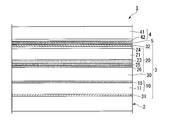
- FIG. 1 is a cross-sectional view of a liquid crystal display device 1 (display device) according to an embodiment of the present invention.
- the liquid crystal display device 1 of the present embodiment includes a backlight 2, a liquid crystal panel 3, and a touch panel 4 (information input device).
- FIG. 1 illustration of the electrode etc. which comprise the liquid crystal panel 3 is abbreviate
- the observer sees the display from the upper side of the liquid crystal display device 1 in FIG. Therefore, in the following description, the side on which the touch panel 4 is disposed is referred to as a viewing side, and the side on which the backlight 2 is disposed is referred to as a back side.
- the light emitted from the backlight 2 is modulated by the liquid crystal panel 3, and a predetermined image, character, or the like is displayed by the modulated light.
- liquid crystal panel 3 an active matrix transmissive liquid crystal panel is described as an example, but a liquid crystal panel applicable to the present invention is not limited to an active matrix transmissive liquid crystal panel.
- the liquid crystal panel applicable to the present invention may be, for example, a transflective (transmission / reflection type) liquid crystal panel, and each pixel is a switching thin film transistor (hereinafter abbreviated as TFT). It may be a simple matrix type liquid crystal panel that does not include
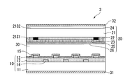
- FIG. 2 is a cross-sectional view of the liquid crystal panel 3.
- the liquid crystal panel 3 includes a TFT array substrate 10 (second substrate) serving as a switching element substrate, and a color filter substrate 20 (first substrate, A display device substrate), a liquid crystal layer 30 sandwiched between the TFT array substrate 10 and the color filter substrate 20, and a pair of polarizing plates 31 and 32 functioning as polarizers.
- the liquid crystal layer 30 includes a TFT array substrate 10, a color filter substrate 20, and a frame-shaped seal member (not shown) that bonds the TFT array substrate 10 and the color filter substrate 20 at a predetermined interval. It is enclosed in the enclosed space.
- the first polarizing plate 31 is disposed on the back side of the liquid crystal panel 3 (on the TFT array substrate 10 side).
- the second polarizing plate 32 is disposed on the viewing side (the color filter substrate 20 side) of the liquid crystal panel 3.
- the liquid crystal panel 3 of the present embodiment performs display in, for example, an IPS (In-Plane Switching) mode.
- a spherical spacer (not shown) is disposed between the TFT array substrate 10 and the color filter substrate 20 to keep the distance between the substrates constant.
- the display mode is not limited to the IPS mode described above, and a TN (Twisted Nematic) mode, a STN (Super Twisted Nematic) mode, a VA (Vertical Alignment, vertical alignment) mode, or the like can be used.
- the TFT array substrate 10 includes a first substrate 11, a gate insulating film 12, a first electrode 13, a second electrode 14, and an alignment film 15.
- the first substrate 11 is made of, for example, glass.
- the first electrode 13 is made of source metal.
- the first electrode 13 is formed on the gate insulating film 12.
- the second electrode 14 is formed of gate metal.
- the second electrode 14 is formed in the gate insulating film 12.
- the first electrode 13 and the second electrode 14 are comb-like electrodes.
- the comb-like electrode has a plurality of electrode portions arranged in parallel with each other at intervals, and a connecting portion for connecting the plurality of electrode portions.
- the alignment film 15 is formed on the first electrode 13 and the gate insulating film 12.
- the first electrodes 13 and the second electrodes 14 are alternately arranged.
- an electric field generated between the first electrode 13 and the second electrode 14 is applied to the liquid crystal layer 30. That is, a lateral electric field substantially parallel to the surface of the first substrate 11 is generated.
- the color filter substrate 20 includes a second substrate 21 (substrate), a black matrix 22, a color filter 23 (wavelength conversion layer), a conductive film 24, a planarization film 25, and an alignment film 26. .
- the second substrate 21 is made of, for example, glass.
- the black matrix 22 is configured, for example, by dispersing carbon in a resin.
- the black matrix 22 is provided on the surface (first surface 21S1) of the second substrate 21 facing the TFT array substrate 10. By adjusting the thickness of the black matrix 22, the blackness (light shielding degree) can be increased or the resistance value can be decreased.
- the color filter 23 is provided in a region partitioned by the black matrix 22 on the first surface 21S1 of the second substrate 21.
- the color filter 23 includes, for example, a red color filter, a green color filter, and a blue color filter.
- the light emitted from the backlight 2 and transmitted through the liquid crystal layer 30 and incident on the color filter substrate 20 substantially perpendicularly is transmitted through the red color filter, the green color filter, and the blue color filter, and the light having the wavelength spectrum of each color light. Transparent. Then, red light, green light, and blue light are emitted from the color filter substrate 20 to the outside. Thereby, full color display is performed.
- the conductive film 24 is formed on a surface 21S2 (second surface) opposite to the first surface 21S1 of the second substrate 21.
- the conductive film 24 is made of, for example, a transparent conductive film material such as indium tin oxide (Indium Tin Oxide, hereinafter referred to as ITO), indium zinc oxide (Indium Zinc Oxide, hereinafter referred to as IZO), ZnO, or the like. Is preferred. This is because it is possible to prevent the transmittance from being impaired by forming the conductive film 24 from a transparent conductive film material.
- the conductive film 24 of this embodiment is made of ITO.
- the conductive film 24 functions as a shield conductive film that shields electromagnetic waves from the liquid crystal panel 3 to the touch panel 4 and external static electricity from affecting the liquid crystal panel 3.
- the potential of the conductive film 24 is set to the ground potential, that is, the same potential as that of the first electrode 13 and the second electrode 14 when no voltage is applied.
- the conductive film 24 is provided on the color filter substrate 20, it is possible to suppress the occurrence of the above problems.
- the conductive film 24 is preferably formed in the entire region contributing to display in the liquid crystal display device 1. Thereby, a more remarkable shielding effect can be obtained. In other words, the conductive film 24 may not be formed in a region that does not contribute to display in the liquid crystal display device 1.
- the planarizing film 25 is formed so as to cover the black matrix 22 and the color filter 23.
- the alignment film 26 is formed on the planarizing film 25.
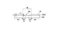
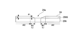
- FIG. 3A and 3B are schematic views of the conductive film 24 formed on one surface 20AS of the display device body 20A constituting the liquid crystal display device 1 of the present embodiment.
- FIG. 3A is a plan view.
- FIG. 3B is a cross-sectional view.
- a defective portion 24a that exposes one surface 20AS of the display device main body 20A exists in a part of the conductive film 24.
- the “defect portion” in the present specification refers to a substrate surface that is necessarily exposed. Others are not called defective parts. For example, a conductive film whose thickness is locally thin is not called a defective portion.
- the conductive film 24 has a first region AR1 located around the defect 24a and a second region AR2 located outside the first region AR1.
- the thickness d of the conductive film 24 in the second region AR2 is substantially constant.
- the thickness dr of the conductive film 24 in the first region AR1 varies between the display device body 20A and the conductive film 24 in the second region AR2.
- the shape of the region including the defect 24a and the first region AR1 has a cross-sectional area when cut along a plane parallel to one surface 20AS of the display device body 20A.
- the shape is large on the side farther from the one side 20AS of 20A (touch panel 4 side) and gradually becomes smaller as it approaches the side 20AS of the display device body 20A (away from the touch panel 4). That is, the region AR has a so-called forward tapered frustum shape when viewed from the display device body 20A side.
- the cross-sectional shape of the inclined portion of the conductive film 24 in the first region AR1 is a linear shape.
- the inclination of the inclined portion of the conductive film 24 in the first region AR1 is constant.
- the conductive film 24 having such an inclined portion can be manufactured by a polishing method described later.
- the backlight 2 emits light toward the liquid crystal panel 3 using a light source (not shown) such as a light emitting diode or a cold cathode tube and internal reflection of light emitted from the light source.
- a light source such as a light emitting diode or a cold cathode tube and internal reflection of light emitted from the light source.
- a light guide plate (not shown).
- the backlight 2 may be an edge light type in which a light source is disposed on an end face of a light guide, or may be a direct type in which a light source is disposed directly below the liquid crystal panel 3.
- the touch panel 4 is attached on the second polarizing plate 32 with an adhesive 5 such as a double-sided tape.
- the touch panel 4 is disposed on the color filter substrate 20 on the side where the conductive film 24 is disposed, in other words, on the viewing side of the liquid crystal panel 3.
- the touch panel 4 includes a base material 41 and a position detection electrode 42.
- the base material 41 consists of glass etc., for example.
- the position detection electrode 42 is made of a transparent electrode material such as ITO or ATO (Antimony-doped Tin Oxide: tin oxide doped with antimony).
- the position detection electrode 42 is formed by sputtering of ITO, ATO or the like, and has a uniform sheet resistance of about several hundred to 2 k ⁇ / ⁇ .
- the capacitive touch panel 4 is adopted.
- minute voltages are applied to four corners of the position detection electrode 42 when the touch panel 4 is viewed in plan.
- the point touched by the finger is grounded via the capacitance of the human body.
- the voltage at each corner changes according to the resistance value between the ground point and the four corners.
- the position detection circuit measures this voltage change as a current change, and detects the ground point, that is, the position touched by the finger from the measured value.
- touch panel applicable to the present embodiment is not limited to the capacitive method, and any touch panel such as a resistive film method, an ultrasonic method, and an optical method can be applied.
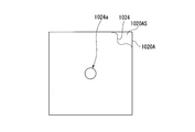
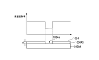
- FIG. 4A and 4B are schematic views of the conductive film 1024 formed on one surface 1020AS of the display device main body 1020A constituting the liquid crystal display device.
- FIG. 4A is a plan view.
- FIG. 4B is a cross-sectional view.
- a defective portion 1024a exists in a part of the conductive film 1024.
- Such a defective portion 1024a is caused, for example, when foreign matter adheres to one surface 1020AS of the display device main body 1020A when the conductive film 1024 is formed in the manufacturing process of the liquid crystal display device.
- Examples of the method for forming the conductive film include sputtering and vapor deposition. For example, consider the case where a conductive film is formed by sputtering.
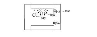
- FIG. 5A to FIG. 5C and FIG. 6A to FIG. 6C are diagrams showing an example of a film forming process when forming the conductive film 1024 by the sputtering method.
- a display device main body 1020A which is a film formation target for forming a conductive film 1024, and a target 1024A made of a material for forming the conductive film 1024 are opposed to each other with a predetermined interval inside a chamber 1050. And place it.
- the chamber 1050 is evacuated and a voltage is applied between the display device body 1020A and the target 1024A.
- electrons and ions 1051 move at high speed and collide with the target 1024A.
- the repelled atoms 1052 collide with and adhere to the display device main body 1020A.
- the conductive film 1024 is formed on one surface of the display device body 1020A.
- the atoms 1052 repelled from the surface of the target 1024A may not only collide and adhere to the display device main body 1020A, but may also collide and adhere to the inner wall of the chamber 1050. Therefore, when the deposition process of the conductive film 1024 is repeatedly performed, the atoms 1052 repelled from the surface of the target 1024 A are accumulated on the inner wall of the chamber 1050. What has accumulated on the inner wall of the chamber 1050 may be peeled off for some reason.
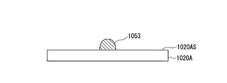
- a part of the film peeled in this way becomes a film-like indeterminate shape lump 1053 (foreign matter), and drops and adheres to one surface 1020AS of the display device main body 1020A.
- the foreign material 1053 there are various other variations such as dust existing inside and outside the chamber 1050.
- a case is considered in which a conductive film 1024 is formed with a foreign substance 1053 attached to one surface 1020AS of the display device main body 1020A.
- the conductive film 1024 is hardly formed on the sidewall of the foreign material 1053. Therefore, the conductive film 1024 is formed in a state where the conductive film 1024 is lifted by the height of the foreign matter 1053 at a portion where the foreign matter 1053 is attached. As a result, the conductive film 1024 is peeled off together with the foreign matter.
- the part (protruding part) that floats in the conductive film 1024 may be peeled off together with the foreign material 1053 in some cases.
- a defective portion 1024a such as a pinhole defect is generated in a part of the conductive film 1024.
- the shape of the defective portion 1024a follows the shape of the foreign matter 1053 attached to the one surface 1020AS of the display device main body 1020A.
- the shape of the defect portion 1024a is also an indefinite shape.
- the defect portion 1024a is a needle-like cavity (pinhole defect) as shown in FIGS. 4A, 4B, and 6C.
- the defective portion 1024a (the surface reflectance of the display device main body 1020A exposed from the conductive film 1024) is different from the surface reflectance of the conductive film 1024 around the defective portion 1024a, the defective portion 1024a. May be recognized as a defective portion of the conductive film 1024. Such a defective portion 1024a is hardly noticeable when the backlight is turned on, but becomes noticeable when the backlight is turned off.
- a visual inspection oblique light inspection
- the defect portion 1024a looks darker than the surrounding conductive film 1024.
- the defect portion 1024a is surrounded by the conductive film 1024. The degree to which it looks darker becomes larger. This is because a portion where the difference in surface reflectance changes sharply is easily recognized by human eyes. As a result, the defective portion 1024a is recognized as a defective portion of the conductive film 1024.
- the display device having the defective part is extracted from the production line and discarded as a defective product.
- discarding the display device is not preferable because it leads to a decrease in yield.
- the defective portion when a defective portion exists in the conductive film, the defective portion is hardly recognized as a defective portion by polishing the conductive film in a predetermined region around the defective portion of the conductive film.
- the method is adopted.
- the manufacturing method of the liquid crystal display device 1 is not limited to this.
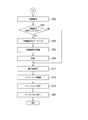
- FIG. 7 and 8 are flowcharts showing the manufacturing process of the liquid crystal display device 1.
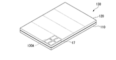
- 9 to 11C are process diagrams sequentially showing the manufacturing process of the liquid crystal display device 1.
- FIG. 7 and 8 are flowcharts showing the manufacturing process of the liquid crystal display device 1.
- the method for manufacturing the liquid crystal display device 1 includes a “first base material substrate manufacturing process” (step S1) and a “second base material substrate forming process” (step S2).
- “Sealant forming process” step S3), “Liquid crystal dropping process” (step S4), “First substrate bonded body manufacturing process” (step S5), and “Second substrate bonded body manufacturing process” (Step S6), “Conductive film forming step (first step)” (Step S7), “First defect inspection step (second step)” (Steps S8 and S9), “Marking process” (Step S10), “Third substrate bonded body manufacturing process” (Step S11), “Second defect inspection process (second process)” (Steps S12, S13), and “Second marking Process “(step S14) and” polishing process (third ”) (Step S15),“ cleaning process ”(step S16),“ polarizing plate attaching process ”(
- the first base material substrate 110 is prepared (prepared) (first base material substrate manufacturing step, step S1 in FIG. 7).
- the first base material substrate 110 is manufactured by forming TFTs, wirings, gate insulating films, comb electrodes, alignment films, and the like on a glass substrate.
- the first base material substrate 110 has a plurality of TFT array substrate formation regions (regions where the TFT array substrate 10 is formed) 110A (see FIG. 9).
- a TFT, a wiring, a gate insulating film, a comb electrode, and an alignment film are formed on the first base material substrate 110.
- the second base material substrate 120 is prepared (prepared) (second base material substrate forming step, step S2 in FIG. 7).
- the second base material substrate 120 is manufactured by forming a black matrix, a color filter, a planarization film, an alignment film, and the like on a glass substrate.
- the second base material substrate 120 has a plurality of color filter substrate forming regions 120A (regions where the color filter substrate 20 is formed) (see FIG. 9).
- a closed annular sealing material 17 is formed in each TFT array substrate forming region 110A of the first base material substrate 110 (sealing material forming step, step S3 in FIG. 7).
- the seal material 17 includes a spherical spacer. The spacer diameter is approximately the same as the cell gap of the substrate.
- the closed annular sealing material 17 is formed on the first base material substrate 110, but the present invention is not limited to this.
- a closed annular sealing material 17 may be formed on the second base material substrate 120 instead of the first base material substrate 110. That is, the closed annular sealing material 17 may be formed on either the first base material substrate 110 or the second base material substrate 120.
- the liquid crystal 30a is discharged and dropped from a dispenser (not shown), and the liquid crystal 30a is disposed in a region surrounded by the sealing material 17 on the first base material substrate 110 as shown in FIG. 9 (liquid crystal dropping step, Step S4 in FIG.
- the manufacturing method of the liquid crystal display device 1 of the present embodiment uses an ODF (One Drop Fill) method.
- the liquid crystal 30a is dropped on the substrate side on which the sealing material 17 is formed, but the present invention is not limited to this.
- the liquid crystal 30a may be dropped on a substrate opposite to the substrate on which the sealing material 17 is formed. That is, the liquid crystal 30a may be dropped corresponding to the region surrounded by the sealing material 17, and the dropping side is the substrate side where the sealing material 17 is formed or the substrate side where the sealing material 17 is not formed. Either of these may be used.
- the first substrate bonded body 130 has a plurality of display device main body forming regions (regions in which the display device main body 20A is formed) 130A.
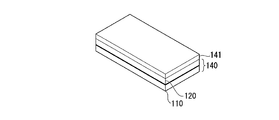
- the first substrate bonded body 130 is divided to produce the second substrate bonded body 140 (second substrate bonded body manufacturing step, step S6 in FIG. 7).
- a cut 130SL (scribe line) is formed between the outer surfaces of the first substrate bonded body 130 and between the adjacent sealing materials 17 (broken line portion in the figure). Then, by applying mechanical stress or thermal stress to the cut 130SL, the first substrate bonded body 130 is divided (scribe break method).
- a plurality of second substrate bonded bodies 140 are produced.
- the first substrate bonded body 130 is divided into strips, and four second substrate bonded bodies 140 are obtained.
- Each of these second substrate bonded bodies 140 has a plurality of display device main body forming regions (regions where the display device main body 20A is formed) 140A.
- substrate bonded body 130 is divided
- the first substrate bonded body 130 may be divided into a cross shape or may be divided into a lattice shape.
- the first substrate bonded body 130 is divided into four second substrate bonded bodies 140, but the present invention is not limited to this.
- the number of divisions when dividing into the second substrate bonded body may be two, three, or a plurality of five or more.
- a conductive film 141 is formed on one surface of the second substrate bonded body 140 (the outer surface of the second base material substrate 120) (conductive film formation step, step S7 in FIG. 7). ).
- the second substrate bonded body 140 is put into a film forming apparatus (chamber) (not shown).
- the first base material substrate 110 is disposed on the seat surface side of the chamber so that the conductive film 141 is formed on the outer surface of the second base material substrate 120.
- the conductive film 141 is formed by evaporation or sputtering using a formation material such as ITO or IZO.
- the conductive film 141 is formed on one surface of each second substrate bonded body 140 cut out from the first substrate bonded body 130. That is, the size (plan view size) of the second substrate bonded body 140 to be formed is smaller than the size of the first substrate bonded body 130. Therefore, handling when the second substrate bonded body 140 is put into the chamber is facilitated.
- substrate bonded body 130 is parted, it is not restricted to this.
- the conductive film may be formed on one surface of the first substrate bonded body 130 in the conductive film forming step without dividing the first substrate bonded body 130.
- a conductive film is formed on one surface of the bonded substrate stack. The reason is that when a conductive film is formed on the outer surface of the second base material substrate before producing the first substrate bonded body, the side of the second base material substrate on which the color filter is formed is the seat surface side of the chamber. This is because the color filter is damaged.
- the inspection of the defect portion is performed by visual inspection (oblique light inspection) in which reflected light is inspected by applying light obliquely to the film formation surface of the conductive film 141 in the second substrate bonded body 140.
- the protruding portion is put together with the foreign matter by a predetermined method. Remove. This is because such a protruding portion is also recognized as a defective portion of the conductive film in the oblique light inspection.
- An example of a method for removing such protruding portions together with foreign substances is a method using laser irradiation. Other methods include brush cleaning using a brush and cleaning with an organic solvent.
- step S9 “Yes” in FIG. 7 the defective portion is marked (first marking step, step S10 in FIG. 7).
- the marking of the defective portion is performed by, for example, surrounding the defective portion in the conductive film 141 with a circle using a pen such as a marker. As a result, a defective portion can be visually recognized during a polishing process described later.
- the second substrate bonded body 140 on which the conductive film 141 is formed is divided (divided into pieces), and a third substrate bonded body 150 is manufactured (third substrate bonded body manufacturing step, in FIG. 7). Step S11).
- the second substrate bonded body 140 on which the conductive film 141 is formed For example, as shown in FIG. 11B, between the outer surface (the outer surface of the conductive film 141 in the present embodiment) of the second substrate bonded body 140 on which the conductive film 141 is formed (see the broken line portion in the figure). ) To form 140SL (scribe line). Then, by applying mechanical stress or thermal stress to the notch 140SL, the second substrate bonded body 140 on which the conductive film 141 is formed is divided (scribe break method).
- substrate bonding body 150 is produced.
- the conductive film 141 is divided, a plurality of conductive films 24 are obtained.
- substrate bonding body 140 is parted, it will become several display apparatus main body 20A.
- step S12 in FIG. 8 it is inspected whether or not there is a defect in the conductive film 24 (second defect inspection step, step S12 in FIG. 8).
- the inspection of the defective part is performed by visual inspection (oblique inspection) in which reflected light is inspected by applying light obliquely to the film formation surface of the conductive film 24 in the display device main body 20A.
- defect inspection step before and after cutting out the plurality of third substrate bonded bodies 150 from the second substrate bonded body 140, it is inspected whether or not there is a defect in the conductive film. That is, in addition to performing defect inspection on the second substrate bonded body 140 (first defect inspection step), defect inspection is also performed on the third substrate bonded body 150 in which the second substrate bonded body 140 is separated. (Second defect inspection step). Therefore, the inspection accuracy of the defective part can be improved.
- defect inspection is performed in each of the first defect inspection process and the second defect inspection process, and the number of defect inspections is two times in total.
- the present invention is not limited to this.
- the number of defect inspections may be one, or three or more.
- step S13 “Yes” in FIG. 8 the defective portion is marked (second marking step, step S14 in FIG. 8).
- the marking of the defective portion is performed by, for example, surrounding the defective portion in the conductive film 141 with a circle using a pen such as a marker. As a result, a defective portion can be visually recognized during a polishing process described later.
- step S13 “No” in FIG. 8 the process proceeds to the polarizing plate pasting step.
- the defective part is polished (step S15 in FIG. 8).
- FIG. 12A to 12C are process diagrams sequentially showing the polishing process of the defective portion.
- a defective portion 24a such as a pinhole defect that exposes one surface 20AS of the display device main body 20A exists in a part of the conductive film 24.
- a polishing agent 60 is applied to the defective portion 24a of the conductive film 24, and the conductive film 24 is polished by rotating the polishing tool 70 while pressing the tip of the polishing device 70 against the defective portion 24a.
- polishing machine 70 for example, a commercially available handy router can be used. Thereby, since it is small and lightweight, handling becomes easy and workability
- polishing can be improved.
- the polishing target is placed on a stage (not shown) and placed horizontally, and the tip of the polishing device 70 is vertically applied to the polishing target from above.
- the arrangement direction of the object to be polished is not limited to the horizontal arrangement.
- the object to be polished may be arranged vertically by leaning against a wall, or may be arranged obliquely.
- the arrangement direction of the object to be polished can be set in various directions.
- the tip of the polishing machine 70 is not limited to being vertically applied to the object to be polished from above.
- the polishing target may be reversed and placed above the work position, and the tip of the polishing device 70 may be applied vertically from below to the polishing target.
- the defective portion of the conductive film may be far from the operator's position, and it may be difficult to apply the tip of the polishing machine 70 to the defective portion.
- the tip of the polishing device 70 can be applied perpendicularly to the object to be polished from below. Therefore, the polishing process using the polishing device 70 can be easily performed.
- the third substrate bonded body 150 is manufactured by dividing the second substrate bonded body 140 into pieces in the third substrate bonded body manufacturing step. Therefore, by using the third substrate bonded body 150 as an object to be polished, handling during polishing becomes easy.
- the size of the third substrate bonded body 150 to be polished is a palm size
- the operator can hold the third substrate bonded body 150 with one hand. For this reason, the polishing process using the polisher 70 can be easily performed.
- substrate bonded body 140 is separated into pieces in the 3rd board
- the defective portion of the conductive film of the second substrate bonded body 140 may be polished in the polishing step without dividing the second substrate bonded body 140 into individual pieces.
- polishing is performed. In the process, the defective portion of the conductive film of the first substrate bonded body 130 may be polished.
- the present invention can be applied even when the size of the object to be polished (plan view size) is larger than the size of the liquid crystal display device 1 (plan view size).
- the present invention is not limited to this.
- a polishing apparatus may be used when polishing the conductive film.
- FIG. 13 is a schematic diagram of the polishing machine 70.
- the grinder 70 includes a main body 71, a rotating member 72, a power supply unit 73, and a rotation speed adjusting unit 74.
- the body portion 71 is a grip portion that becomes a portion to be gripped by a hand.
- the rotating member 72 is provided at the tip of the main body 71.
- the power supply unit 73 is provided at the base end of the main body unit 71.
- the rotation speed adjustment unit 74 is provided on the base end side of the main body 71. The rotation speed adjustment unit 74 can adjust the rotation speed optimal for the member attached to the rotation member 72 and the conditions of the object to be polished (conductive film 24).
- the polishing of the conductive film 24 can be performed, for example, under the following conditions.
- the rotational speed of the rotating member 72 of the polishing machine 70 is set within the range of 2000 rpm to 5000 rpm.
- the load applied to the conductive film 24 is set within the range of 70 g to 100 g.
- the polishing time is set within the range of 5 to 30 seconds.
- the conductive film 24 is polished in a state where cotton 75 rounded into a spherical shape is attached to the rotating member 72 of the polishing device 70.
- the diameter of the cotton 75 is about 2.5 mm to 5.0 mm in accordance with the size of the defect portion 24a.
- the conductive film 24 is scraped off according to the surface shape of the hard member. Therefore, it becomes difficult to make the shape of the conductive film 24 around the defect 24a into a desired shape.
- cotton 75 that is more flexible than the conductive film 24 is used as a member that is attached to the rotating member 72 of the polishing machine 70.
- the cotton 75 is crushed during polishing and has an appropriate curvature. Therefore, it becomes easy to make the shape of the conductive film around the defect 24a a desired shape.
- the shape of a defect part has many indefinite shapes
- the area in planar view of a defect part has a thing of about 1 mm ⁇ 2 > or less. Therefore, if a spherical cotton 75 having a diameter of about 2.5 mm to 5.0 mm is polished in a state where it is attached to the rotating member 72 of the polisher 70, even if it is a defect portion of a wide variety of shapes, The conductive film can be gently polished.
- Cotton 75 is suitable because it can be used repeatedly.
- the polishing agent 60 for example, a commercially available plastic compound for mirror finishing can be used. Thereby, since the particle
- FIG. 1 A commercially available plastic compound for mirror finishing can be used.
- the surface of the display device body 20A may be polished together.
- the surface of the display device main body 20 ⁇ / b> A is also finished to a mirror like the conductive film 24. Therefore, there is no visual problem even if the surface of the display device main body 20A is polished.
- the thickness dr of the conductive film 24 in the first area AR1 can be gently changed between the display device body 20A and the conductive film 24 in the second area AR2.
- polishing portion is cleaned (cleaning step, step S16 shown in FIG. 8).
- cleaning step step S16 shown in FIG. 8
- the compound or polishing powder remaining after polishing is washed away with water.
- a pair of polarizing plates 31 and 32 are attached to the display device body 20A on which the conductive film 24 is formed (polarizing plate attaching step, step S17 shown in FIG. 8).
- the 1st polarizing plate 31 is affixed on the back side of the said display apparatus main body 20A.
- the 2nd polarizing plate 32 is affixed on the visual recognition side of the said display apparatus main body 20A. Thereby, the liquid crystal panel 3 is produced.
- driver IC (not shown) is mounted on the liquid crystal panel 3 (driver IC mounting step, step S18 shown in FIG. 8).
- the backlight 2 is attached to the liquid crystal panel 3 on which the driver IC is mounted (backlight attachment process, step S19 shown in FIG. 8).
- the backlight 2 is attached to the back side of the liquid crystal panel 3.
- the touch panel 4 is attached to the liquid crystal panel 3 to which the backlight 2 is attached using, for example, an adhesive 5 such as a double-sided tape (touch panel attachment step, step S20 shown in FIG. 8).
- the touch panel 4 is attached to the viewing side of the liquid crystal panel 3.
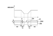
- FIG. 14A and 14B are diagrams showing the relationship between the thickness of the conductive film and the surface reflectance of the conductive film.
- FIG. 14A is a diagram showing a relationship between the thickness of the conductive film 1024 and the surface reflectance of the conductive film 1024 in the comparative example.
- FIG. 14B is a diagram showing the relationship between the thickness of the conductive film 24 and the surface reflectance of the conductive film 24 in the present embodiment.
- the upper graph is a graph showing the surface reflectance of the defective portion of the conductive film and the surface reflectance of the conductive film around the defective portion.
- the lower part is a cross-sectional view of the conductive film formed on one surface of the display device body.
- the horizontal axis indicates the position on the axis parallel to the in-plane direction of one surface of the display device body.
- the vertical axis represents the surface reflectance.
- the thickness of the conductive film 1024 and the surface reflectance of the conductive film 1024 there is a certain correspondence between the thickness of the conductive film 1024 and the surface reflectance of the conductive film 1024.
- the thickness dX of the conductive film 1024 around the defect portion 1024a is substantially constant.
- the surface reflectance of the conductive film 1024 is substantially constant.
- the difference between the surface reflectance of the defect portion 1024a and the surface reflectance of the conductive film 1024 changes the side wall almost vertically at the boundary portion between the defect portion 1024a and the conductive film 1024. Therefore, in the comparative example, in the oblique light inspection, the degree to which the defective portion 1024a appears darker than the surrounding conductive film 1024 increases.
- the conductive film 24 of the present embodiment has a substantially constant surface reflectance of the conductive film 24 in the second region AR2, and the surface reflection of the conductive film 24 in the first region AR1. It differs from the conductive film of the comparative example in that the rate changes between the surface reflectance of the display device main body 20A (substrate) and the surface reflectance of the conductive film 24 in the second region AR2.
- the surface reflectance of the conductive film 24 of the present embodiment is between the surface reflectance of the display device main body 20A (substrate) and the surface reflectance of the conductive film 24 in the second region AR2, and the first region. It is not constant within AR1.
- the thickness d of the conductive film 24 in the second region AR2 is substantially constant.
- the thickness dr of the conductive film 24 in the first region AR1 varies from 0 to the conductive film 24 in the second region AR2.
- the thickness dr of the conductive film 24 in the first region AR1 is larger than 0 and smaller than the thickness of the conductive film 24 in the second region AR2, and is not constant in the first region AR1.
- the inventor of the present application has determined that the degree of recognition of the defective portion 24a as a defective portion in the conductive film 24 and the ratio of the thickness d to the distance L (d / L) when the polishing process is performed. And found that there is a certain relationship between.
- the thickness d is the thickness of the conductive film 24 in the second region AR2.
- the distance L is a distance from the boundary portion between the conductive film 24 and the defect portion 24a to the boundary portion between the first region AR1 and the second region AR2.
- the sample used was one in which a conductive film 24 (thickness 20 nm) was formed by sputtering on one surface 20AS of the display device main body 20A.
- a defective portion 24 a exists in a part of the conductive film 24, and the conductive film 24 is polished in the first region AR 1 around the defective portion 24 a of the conductive film 24. Polishing of the conductive film 24 was performed by applying an abrasive 60 to the defective portion 24a of the conductive film 24 and rotating the polishing tool 70 while pressing the tip of the polishing device 70 against the defective portion 24a.
- polishing device 70 Polishing of the conductive film 24 was performed in a state where a cotton 75 rounded into a spherical shape having a diameter of about 2.5 mm to 5.0 mm was attached to the rotating member 72 of the polishing machine 70.
- Polishing conditions were set as follows. The number of rotations of the rotating part of the rotating member was set in the range of 2000 rpm to 5000 rpm. The load applied to the conductive film was set within the range of 70 to 100 g. The polishing time was set within the range of 5 to 30 seconds.
- the distance L in the sample (1) was 0.1 mm or less.
- the defect 24a was recognized as a defective portion of the conductive film 24 in the oblique light inspection. The reason for this is considered to be as follows.
- the first area AR1 becomes too narrow. That is, the difference between the surface reflectance of the defective portion 24a (the surface reflectance of the display device main body 20A) and the surface reflectance of the conductive film 24 changes sharply at the boundary portion between the defective portion 24a and the conductive film 24. . Therefore, in the oblique light inspection, the degree to which the defective portion 24 a appears darker than the surrounding conductive film 24 is increased, and the defective portion 24 a is recognized as a defective portion of the conductive film 24.
- the lower limit value of the distance L for avoiding the defective portion 24a being recognized as a defective portion in the oblique light inspection is 0.1 mm.
- the distance L in the sample (2) was greater than 0.1 mm and within a range of 0.2 mm or less.
- the defect portion 24a was hardly recognized as a defective portion of the conductive film 24 in the oblique light inspection.
- the distance L in the sample (3) was larger than 0.2 mm and less than 2.0 mm.
- the defect 24a was not recognized as a defective portion of the conductive film 24 in the oblique light inspection.
- the distance L in sample (4) was in the range of 2.0 mm or more and less than 2.5 mm.
- the defect portion 24a was hardly recognized as a defective portion of the conductive film 24 in the oblique light inspection.
- the distance L in sample (5) was 2.5 mm or more.
- the defect 24a was recognized as a defective portion of the conductive film 24 in the oblique light inspection. The reason for this is considered to be as follows.
- the distance L is increased. It is effective. However, if the distance L is too long, the first area AR1 becomes too wide. That is, the region where the surface reflectance is small in the conductive film 24 becomes too wide. Therefore, the conductive film 24 in the first region AR1 appears to be relatively dark, and is recognized as a defective portion of the conductive film 24.
- the upper limit value of the distance L for preventing the conductive film 24 in the first region AR1 from being recognized as a defective portion is 2.5 mm.
- the thickness of the conductive film 24 is preferably set from the viewpoint of suppressing the occurrence of interference due to multiple reflection of light.
- the refractive index of the conductive film 24 is n
- the thickness of the conductive film 24 in the second region is d
- the wavelength of light incident on the conductive film from the outside is ⁇
- the following equation (3) is satisfied. Is preferred. 2nd ⁇ / 2 (3)
- FIG. 15 is a diagram illustrating a state in which external light is perpendicularly incident on the conductive film 24.
- two light bundles (light L1 reflected from the upper surface of the conductive film 24 and light L2 reflected from the lower surface of the conductive film 24) out of the external light including a plurality of light bundles are shown. .
- light perpendicularly incident on the conductive film 24 is divided into light L ⁇ b> 1 reflected from the upper surface of the conductive film 24 and light L ⁇ b> 2 reflected from the lower surface of the conductive film 24.
- the light L1 reflected from the upper surface and the light L2 reflected from the lower surface interfere with each other and appear bright or dark. That is, interference fringes can be seen.
- the case where it looks bright is a case where the phases of the light L1 reflected from the upper surface and the light L2 reflected from the lower surface match and strengthen each other.
- Light that travels through a medium (air) having a low refractive index and is reflected by a medium (conductive film) having a high refractive index is shifted by ⁇ .
- the waves strengthen when the optical path difference between the light L1 reflected from the upper surface and the light L2 reflected from the lower surface is (m + 1/2) ⁇ .
- the thickness d of the conductive film 24 in the second region AR2 is about 20 nm.
- the refractive index n of the conductive film 24 (ITO) is about 2.2.
- the wavelength of visible light is in the range of 380 nm to 780 nm. Therefore, when the thickness d of the conductive film 24 in the second region AR2 is about 20 nm, the above expression (3) is satisfied.
- the thickness d of the conductive film 24 in the second region AR2 is not limited to about 20 nm, and can be adjusted as appropriate within a range satisfying the above-described expression (3).
- the difference between the surface reflectance of the conductive film 24 and the surface reflectance of the defect 24a in the second region AR2 is about 3.8%.
- the surface reflectance of the conductive film 24 (ITO) in the second area AR2 is about 7.8%.
- the surface reflectance of the defect 24a is about 4%.
- the difference between the surface reflectance of the conductive film 24 and the surface reflectance of the defect 24a in the second region AR2 is about 3.8%.
- “about 3.8%” is a concept including an error of a difference between the surface reflectance of the conductive film 24 and the surface reflectance of the defect 24a in the second region AR2.
- the error include an error caused by a manufacturing process of the conductive film 24 and the like.
- the difference between the surface reflectance of the conductive film 24 and the surface reflectance of the defect portion 24a in the second region AR2 includes a range of 3.5% to 4.1%.
- the conductive film 24 is ITO.
- the same effect can be obtained when the conductive film 24 is IZO.
- the difference between the surface reflectance of the conductive film 24 and the surface reflectance of the defect 24a in the second region AR2 is about 3.5%.
- the surface reflectance of the conductive film 24 (IZO) in the second region is about 7.5%.
- the surface reflectance of the defect 24a is about 4%.
- the difference between the surface reflectance of the conductive film 24 and the surface reflectance of the defect 24a in the second region is about 3.5%.
- “about 3.5%” is a concept including an error of a difference between the surface reflectance of the conductive film 24 and the surface reflectance of the defect 24a in the second region AR2.
- the error include an error caused by a manufacturing process of the conductive film 24 and the like.
- the difference between the surface reflectance of the conductive film 24 and the surface reflectance of the defect 24a in the second region AR2 includes a range of 3.2% to 3.8%.
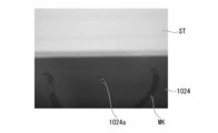
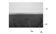
- FIG. 16A and FIG. 16B are photographs in which defective portions of the conductive film are imaged.
- FIG. 16A is a photograph of the defective portion 1024a of the conductive film 1024 in the comparative example.
- FIG. 16B is a photograph of the defect 24a of the conductive film 24 in the present embodiment.
- the symbol ST is a stage for mounting the display device main body.
- the symbol MK is a marking drawn around the defect portion.
- the defect portion 1024a looks clearly darker than the surrounding conductive film 1024. This is presumably because the difference between the surface reflectance of the defect portion 1024a and the surface reflectance of the conductive film 1024 changes sharply at the boundary portion between the defect portion 1024a and the conductive film 1024.
- the defect 24a is almost the same as the degree of darkness of the surrounding conductive film 24. Therefore, it is difficult for the defective portion 24 a to be distinguished from the surrounding conductive film 24.
- the reason is that the surface reflectance of the conductive film 24 in the first region AR1 is the surface reflectance of the defective portion 24a (the surface reflectance of the display device body 20A) and the surface reflectance of the conductive film 24 in the second region AR2. This is thought to be due to the gentle changes between them.
- the thickness dr of the conductive film 24 in the first region AR1 satisfies the above-described formulas (1) to (3), so that the conductivity in the display device main body 20A and the second region AR2 is achieved. It changes gently between the membrane 24. For this reason, the periphery of the defect 24a is blurred as in the captured image. This makes it difficult to distinguish the defective portion 24a from the surrounding conductive film 24. Thus, according to the present embodiment, it is possible to make it difficult to recognize the defective portion 24a as a defective portion.
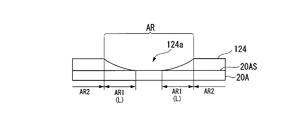
- FIG. 17A is a cross-sectional view illustrating a first modification of a defective portion.
- the region AR has a forward tapered frustum shape when viewed from the display device body 20A side. That is, the cross-sectional shape of the inclined portion of the conductive film 24 in the first region AR1 is a linear shape.
- the region AR of this modification has a curved shape in which the shape of the inclined portion of the conductive film 124 in the first region AR1 is concave. In other words, the gradient of the inclined portion of the conductive film 124 in the first region AR1 gradually increases as the distance from the one surface 20AS of the display device body 20A increases.
- the shape of the area AR in this modification is such that the cross-sectional area when cut along a plane parallel to the one surface 20AS of the display device main body 20A is large on the side far from the one surface 20AS of the display device main body 20A.
- the shape gradually decreases as it approaches.
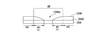
- FIG. 17B is a cross-sectional view showing a second modification of the defect portion.
- the region AR of this modification has a curved shape in which the shape of the inclined portion of the conductive film 124A in the first region AR1 is convex.
- the gradient of the inclined portion of the conductive film 124A in the first region AR1 gradually decreases as the distance from the one surface 20AS of the display device body 20A increases.
- the cross-sectional area of the first area AR1 when cut along a plane parallel to the one surface 20AS of the display device main body 20A is small on the side far from the one surface 20AS of the display device main body 20A, and the one surface 20AS of the display device main body 20A.
- the shape gradually increases as it approaches.
- FIG. 17C is a cross-sectional view showing a third modification of the defective portion.
- the shape of the inclined portion of the conductive film 124 in the first region AR1 has a shape including a plurality of irregularities.
- the cross-sectional area of the first area AR1 when cut along a plane parallel to the one surface 20AS of the display device body 20A is the smallest on the side far from the one surface 20AS of the display device body 20A. Further, the cross-sectional area of the first area AR1 when cut along a plane parallel to the one surface 20AS of the display device main body 20A varies between the one surface 20AS and the far side of the display device main body 20A and the one surface 20AS of the display device main body 20A. is doing.
- the shape of the area AR is not limited to the shape shown in the modification example, and various shapes can be adopted.
- the liquid crystal display device of the above embodiment can be applied to various electronic devices.
- an electronic apparatus including the liquid crystal display device will be described with reference to FIGS.
- the liquid crystal display device can be applied to, for example, a mobile phone shown in FIG.
- a cellular phone 240 illustrated in FIG. 18 includes a voice input unit 241, a voice output unit 242, an antenna 243, an operation switch 244, a display unit 245, a housing 246, and the like.
- the liquid crystal display device can be preferably applied as the display unit 245. By applying the liquid crystal display device to the display portion 245 of the total mobile phone 240, it is possible to achieve high quality with excellent appearance.
- the liquid crystal display device can be applied to, for example, a portable game machine shown in FIG.
- a portable game machine 260 illustrated in FIG. 19 includes operation buttons 261 and 262, an external connection terminal 263, a display portion 264, a housing 265, and the like.
- the liquid crystal display device can be preferably applied as the display unit 264. By applying the liquid crystal display device to the display portion 264 of the portable game machine 260, the liquid crystal display device can have high quality with excellent appearance.
- the liquid crystal display device can be applied to, for example, a tablet terminal shown in FIG.
- a tablet terminal 280 illustrated in FIG. 20 includes a display unit (touch panel) 281, a camera 282, a housing 283, and the like.
- the liquid crystal display device can be preferably applied as the display unit 281.
- the present invention is applicable to various display devices such as a liquid crystal display device, an organic electroluminescence display device, a plasma display, an LED display, and a MEMS display.
- SYMBOLS 1 Liquid crystal display device (display device), 4 ... Touch panel (information input device), 10 ... TFT array substrate (2nd substrate), 13 ... 1st electrode, 14 ... 2nd electrode, 20 ... Color filter substrate (1st) 1 substrate, display device substrate), 20A ... display device body, 20AS ... one surface of the display device body, 21 ... second substrate (substrate), 21S1 ... first surface, 21S2 ... second surface, 23 ... color filter ( Wavelength conversion layer), 24 ... conductive film, 24a ... defective portion, 30 ... liquid crystal layer, 60 ... abrasive, 72 ... rotating member, 75 ... cotton, 140 ... second substrate bonded body (base material), AR1 ...
Landscapes
- Engineering & Computer Science (AREA)
- Devices For Indicating Variable Information By Combining Individual Elements (AREA)
- Chemical & Material Sciences (AREA)
- Ceramic Engineering (AREA)
- Inorganic Chemistry (AREA)
- Mechanical Engineering (AREA)
- Liquid Crystal (AREA)
Abstract
導電膜(24)の一部には表示装置本体の一面を露出させる欠陥部(24a)が存在しており、導電膜(24)は、欠陥部(24a)の周囲に位置する第1領域(AR1)と第1領域(AR1)の外側に位置する第2領域(AR2)とを有し、第2領域(AR2)における導電膜(24)の表面反射率が略一定であり、第1領域(AR1)における導電膜(24)の表面反射率が基板の表面反射率と第2領域(AR2)における導電膜(24)の表面反射率との間であり、かつ前記第1領域(AR1)内において一定でない。
Description
本発明は、表示装置用基板、表示装置および表示装置の製造方法に関するものである。
本願は、2012年2月28日に、日本に出願された特願2012-041756号に基づき優先権を主張し、その内容をここに援用する。
本願は、2012年2月28日に、日本に出願された特願2012-041756号に基づき優先権を主張し、その内容をここに援用する。
近年、テレビ、パーソナルコンピューター、情報端末機器などに搭載されるディスプレイの高性能化の要求が高まっている。ブラウン管ディスプレイ、液晶ディスプレイ、プラズマディスプレイ、有機ELディスプレイなど様々なタイプの表示装置の研究開発が進められている。
このような表示装置においては、不要輻射を低減させるため、あるいは表示装置の性能特性を向上させるための保護膜が表示装置本体の一面に設けられている。中でも、外部からの静電気をシールドするための導電膜が表示装置の表示ムラを抑制するための保護膜として広く用いられている。
ところで、表示装置の製造工程において、導電膜の一部に表示装置本体の一面を露出させる欠陥部(ピンホール欠陥)が形成される場合がある。このような欠陥部の表面反射率は、当該欠陥部の周囲の導電膜の表面反射率と異なる場合がある。その場合、欠陥部が導電部の不良部分として認識されることがある。
例えば、表示装置における導電膜の成膜面に光を斜めから当てて反射光を検査する目視検査を行う場合を考える。この場合、欠陥部の表面反射率が導電膜の表面反射率よりも小さいと、欠陥部が周囲の導電膜よりも暗く見える。そこで、導電膜の一部に欠陥部が存在している場合において当該欠陥部を補修するための技術の要求が高まっている。
この要求に対して、例えば特許文献1では、皮膜層の一部にピンホール欠陥が存在している場合、皮膜層の上に封止材を塗工してピンホール欠陥を封止材で充填し、当該封止材を硬化させて硬化層を形成し、当該硬化層のうちピンホール欠陥からはみ出た余剰部分を除去する方法が開示されている。
このような方法によれば、ピンホール欠陥が不良部分として認識されにくくなると記載されている。そのためには、皮膜層上における硬化層の余剰部分をきれいに除去する必要がある。皮膜層上において硬化層の余剰部分が残存していると、硬化層の余剰部分が不良部分として認識されてしまうからである。しかしながら、硬化層の余剰部分をきれいに除去することは、非常に精密な研磨を要するため容易ではない。
また、ピンホール欠陥を封止材で充填したり硬化層の余剰部分を除去したりするといった加工には手間がかかる。さらに、封止材の材料費等のコストがかかるという問題もある。
また、ピンホール欠陥を封止材で充填したり硬化層の余剰部分を除去したりするといった加工には手間がかかる。さらに、封止材の材料費等のコストがかかるという問題もある。
本発明は、上記の課題を解決するためになされたものであって、欠陥部を不良部分として認識されにくくすることが可能な表示装置用基板、表示装置および表示装置の製造方法を提供することを目的とする。また、この他にも、簡単な方法でかつ高コスト化を抑制することが可能な表示装置用基板、表示装置および表示装置の製造方法を提供することを目的とする。
上記の目的を達成するために、本発明の表示装置用基板は、第1面と第2面とを有する基板と、前記基板の前記第1面の上に形成された波長変換層と、前記基板の前記第2面に形成された導電膜と、を含み、前記導電膜は前記基板の前記第2面を露出させる欠陥部を有しており、前記導電膜は、前記欠陥部の周囲に位置する第1領域と前記第1領域の外側に位置する第2領域とを有し、前記第2領域における前記導電膜の表面反射率が略一定であり、前記第1領域における前記導電膜の表面反射率が前記基板の表面反射率と前記第2領域における前記導電膜の表面反射率との間であり、前記導電膜の表面反射率が前記第1領域内において一定でないことを特徴とする。
本発明の表示装置用基板は、前記第2領域における前記導電膜の厚みが略一定であり、前記第1領域における前記導電膜の厚みが0より大きく前記第2領域における前記導電膜の厚みより小さく、前記導電膜の厚みが前記第1領域内において一定でないことを特徴とする。
本発明の表示装置用基板は、前記第2領域における前記導電膜の厚みをd、前記導電膜と前記欠陥部との境界部分から前記第1領域と前記第2領域との境界部分までの距離をLとしたとき、下記の(1)式を満たすことを特徴とする。
8×10⁻⁶<(d/L)<2×10-4 ・・・(1)
8×10⁻⁶<(d/L)<2×10-4 ・・・(1)
本発明の表示装置用基板は、前記第2領域における前記導電膜の厚みをd、前記導電膜と前記欠陥部との境界部分から前記第1領域と前記第2領域との境界部分までの距離をLとしたとき、下記の(2)式を満たすことを特徴とする。
1×10⁻⁵<(d/L)<1×10-4 ・・・(2)
1×10⁻⁵<(d/L)<1×10-4 ・・・(2)
本発明の表示装置用基板は、前記導電膜の屈折率をn、前記第2領域における前記導電膜の厚みをd、外部から前記導電膜に入射する光の波長をλとしたとき、下記の(3)式を満たすことを特徴とする。
2nd<λ/2 ・・・(3)
2nd<λ/2 ・・・(3)
本発明の表示装置用基板は、前記導電膜がシールド導電膜であることを特徴とする。
本発明の表示装置用基板は、前記導電膜が透明導電膜であることを特徴とする。
本発明の表示装置用基板は、前記導電膜がインジウム錫酸化物またはインジウム亜鉛酸化物であることを特徴とする。
本発明の表示装置用基板は、前記導電膜がインジウム錫酸化物であるとき、前記第2領域における前記導電膜の表面反射率と前記基板の表面反射率との差が約3.8%であることを特徴とする。
本発明の表示装置用基板は、前記導電膜がインジウム亜鉛酸化物であるとき、前記第2領域における前記導電膜の表面反射率と前記基板の表面反射率との差が約3.5%であることを特徴とする。
本発明の表示装置用基板は、前記波長変換層がカラーフィルターであることを特徴とする。
本発明の表示装置は、前記表示装置用基板を含むことを特徴とする。
本発明の表示装置は、前記表示装置用基板からなる第1の基板と、前記表示装置用基板の前記波長変換層に対向して配置された第2の基板と、前記第1の基板と前記第2の基板との間に挟持された液晶層と、を含むことを特徴とする。
本発明の表示装置は、前記第2の基板の前記表示装置用基板と対向する面の上に、前記液晶層に電界を生じさせる第1電極と第2電極とが設けられていることを特徴とする。
本発明の表示装置は、前記表示装置用基板の前記導電膜の側に、情報入力装置が設けられていることを特徴とする。
本発明の表示装置の製造方法は、表示装置本体の一面に導電膜を成膜する第1の工程と、前記導電膜において前記表示装置本体の前記一面を露出させる欠陥部が存在しているか否かを検査する第2の工程と、前記欠陥部が存在しているときに、前記導電膜の前記欠陥部の周囲の第1領域において前記導電膜を研磨し、前記第1領域における前記導電膜の表面反射率を前記基板の表面反射率と前記第2領域における前記導電膜の表面反射率との間で変化させる第3の工程と、を有することを特徴とする。
本発明の表示装置の製造方法は、前記第3の工程において、前記導電膜の前記欠陥部に研磨剤を塗布し、回転部材の先端を前記欠陥部に押し当てつつ回転させることにより前記導電膜を研磨することを特徴とする。
本発明の表示装置の製造方法は、前記第3の工程において、前記研磨剤としてプラスチック用コンパウンドを用いることを特徴とする。
本発明の表示装置の製造方法は、前記第3の工程において、前記導電膜の前記欠陥部と前記回転部材の先端との間に、綿またはウレタンを配置することを特徴とする。
本発明の表示装置の製造方法は、母材から複数の前記表示装置本体を切り出すことを特徴とする。
本発明の表示装置の製造方法は、前記第1の工程において、切り出された個々の前記表示装置本体の一面に前記導電膜を成膜することを特徴とする。
本発明の表示装置の製造方法は、前記母材から前記複数の表示装置本体を切り出す前後で、前記導電膜において前記欠陥部が存在しているか否かを検査することを特徴とする。
本発明の表示装置の製造方法は、前記表示装置が液晶表示装置であることを特徴とする。
本発明によれば、欠陥部を不良部分として認識されにくくすることが可能な表示装置用基板、表示装置および表示装置の製造方法を提供することができる。簡単な方法でかつ高コスト化を抑制することが可能な表示装置用基板、表示装置および表示装置の製造方法を提供することができる。
以下、本発明の一実施形態について、図1、図2を用いて説明する。
本実施形態では、表示装置として透過型の液晶パネルを備えた液晶表示装置の例を挙げて説明する。
なお、以下の全ての図面においては、各構成要素を見やすくするため、構成要素によって寸法の縮尺を異ならせて示すことがある。
本実施形態では、表示装置として透過型の液晶パネルを備えた液晶表示装置の例を挙げて説明する。
なお、以下の全ての図面においては、各構成要素を見やすくするため、構成要素によって寸法の縮尺を異ならせて示すことがある。
図1は、本発明の一実施形態に係る液晶表示装置1(表示装置)の断面図である。
本実施形態の液晶表示装置1は、図1に示すように、バックライト2と、液晶パネル3と、タッチパネル4(情報入力装置)と、を備えている。
本実施形態の液晶表示装置1は、図1に示すように、バックライト2と、液晶パネル3と、タッチパネル4(情報入力装置)と、を備えている。
なお、図1では、液晶パネル3を構成する電極等の図示を省略しているが、その詳細な構造については後述する。観察者は、タッチパネル4が配置された図1における液晶表示装置1の上側から表示を見ることになる。よって、以下の説明では、タッチパネル4が配置された側を視認側と称し、バックライト2が配置された側を背面側と称する。
本実施形態の液晶表示装置1においては、バックライト2から射出された光を液晶パネル3で変調し、変調した光によって所定の画像や文字等を表示する。
以下、液晶パネル3の具体的な構成について説明する。
ここでは、アクティブマトリクス方式の透過型液晶パネルを一例に挙げて説明するが、本発明に適用可能な液晶パネルはアクティブマトリクス方式の透過型液晶パネルに限るものではない。本発明に適用可能な液晶パネルは、例えば半透過型(透過・反射兼用型)液晶パネルであっても良く、更には、各画素がスイッチング用薄膜トランジスタ(Thin Film Transistor,以下、TFTと略記する)を備えていない単純マトリクス方式の液晶パネルであっても良い。
ここでは、アクティブマトリクス方式の透過型液晶パネルを一例に挙げて説明するが、本発明に適用可能な液晶パネルはアクティブマトリクス方式の透過型液晶パネルに限るものではない。本発明に適用可能な液晶パネルは、例えば半透過型(透過・反射兼用型)液晶パネルであっても良く、更には、各画素がスイッチング用薄膜トランジスタ(Thin Film Transistor,以下、TFTと略記する)を備えていない単純マトリクス方式の液晶パネルであっても良い。
図2は、液晶パネル3の断面図である。
液晶パネル3は、図2に示すように、スイッチング素子基板としてのTFTアレイ基板10(第2の基板)と、TFTアレイ基板10に対向して配置されたカラーフィルター基板20(第1の基板、表示装置用基板)と、TFTアレイ基板10とカラーフィルター基板20との間に挟持された液晶層30と、偏光子として機能する一対の偏光板31,32と、を備えている。
液晶パネル3は、図2に示すように、スイッチング素子基板としてのTFTアレイ基板10(第2の基板)と、TFTアレイ基板10に対向して配置されたカラーフィルター基板20(第1の基板、表示装置用基板)と、TFTアレイ基板10とカラーフィルター基板20との間に挟持された液晶層30と、偏光子として機能する一対の偏光板31,32と、を備えている。
なお、液晶層30は、TFTアレイ基板10と、カラーフィルター基板20と、TFTアレイ基板10とカラーフィルター基板20とを所定の間隔をおいて貼り合わせる枠状のシール部材(図示略)と、によって囲まれた空間内に封入されている。
また、第1偏光板31は、液晶パネル3の背面側(TFTアレイ基板10の側)に配置されている。一方、第2偏光板32は、液晶パネル3の視認側(カラーフィルター基板20の側)に配置されている。
本実施形態の液晶パネル3は、例えばIPS(In-Plane Switching)モードで表示を行うものである。TFTアレイ基板10とカラーフィルター基板20との間には、これら基板間の間隔を一定に保持するための球状のスペーサー(図示略)が配置されている。なお、表示モードについては、上記のIPSモードに限らず、TN(Twisted Nematic)モード、STN(Super Twisted Nematic)モード、VA(Vertical Alignment,垂直配向)モード等を用いることができる。
TFTアレイ基板10は、第1基板11と、ゲート絶縁膜12と、第1電極13と、第2電極14と、配向膜15と、を備えている。
第1基板11は、例えばガラス等からなる。第1電極13は、ソースメタルにより形成されている。第1電極13は、ゲート絶縁膜12上に形成されている。一方、第2電極14は、ゲートメタルにより形成されている。第2電極14は、ゲート絶縁膜12内に形成されている。第1電極13及び第2電極14は、櫛歯状の電極である。櫛歯状の電極は、間隔を空けて互いに平行に配置された複数の電極部と、複数の電極部を連結する連結部と、を有している。
配向膜15は、第1電極13上およびゲート絶縁膜12上に形成されている。
TFTアレイ基板10において、第1電極13と第2電極14とは、交互に配置されている。このような構成により、液晶表示装置1では、第1電極13と第2電極14との間で生じる電界が液晶層30に付与されるようになっている。すなわち、第1基板11の表面と概ね平行な横電界が発生する。
カラーフィルター基板20は、第2基板21(基板)と、ブラックマトリクス22と、カラーフィルター23(波長変換層)と、導電膜24と、平坦化膜25と、配向膜26と、を備えている。
第2基板21は、例えばガラス等からなる。ブラックマトリクス22は、例えば、樹脂中にカーボンを分散して構成されている。ブラックマトリクス22は、第2基板21のTFTアレイ基板10と対向する面(第1面21S1)上に設けられている。ブラックマトリクス22の厚みを調節することで、黒色度(遮光度)を上げたり抵抗値を下げたりすることができる。
カラーフィルター23は、第2基板21の第1面21S1上においてブラックマトリクス22によって区画された領域に設けられている。カラーフィルター23は、例えば、赤色カラーフィルター、緑色カラーフィルター及び青色カラーフィルターを備えている。バックライト2から射出され、液晶層30を透過してカラーフィルター基板20に概ね垂直に入射した光は、赤色カラーフィルター、緑色カラーフィルター及び青色カラーフィルターを透過して各色光の波長スペクトルの光が透過される。そして、赤色光、緑色光および青色光がカラーフィルター基板20から外部に射出される。これにより、フルカラー表示が行われる。
導電膜24は、第2基板21の第1面21S1とは反対側の面21S2(第2面)に形成されている。導電膜24は、例えば、インジウム錫酸化物(Indium Tin Oxide,以下ITOと称する)、インジウム亜鉛酸化物(Indium Zinc Oxide,以下IZOと称する)、ZnO等の透明導電膜材料により形成されていることが好ましい。導電膜24を透明導電膜材料で形成することにより、透過率が損なわれることを抑制することができるからである。本実施形態の導電膜24はITOにより形成されている。
導電膜24は、液晶パネル3からタッチパネル4への電磁波や外部からの静電気が液晶パネル3に影響することを遮蔽するシールド導電膜として機能する。例えば、導電膜24の電位をグランド電位、つまり、電圧無印加状態における第1電極13及び第2電極14と同じ電位にする。これにより、液晶分子の帯電により液晶分子の配向に乱れが生じることを抑制し、輝度の変動が生じることを抑制することができる。
仮に、IPSモードで表示を行う液晶パネルにおいて、カラーフィルター基板に導電膜が設けられていない場合を考える。この場合、静電気が液晶パネル内に影響し、静電気に液晶分子が応答してしまい、輝度の変動が生じることがある。例えば、静電気を帯びた物体を液晶パネルに接触させると、特に黒表示時に光漏れが発生し、コントラストの低下といった表示不良が発生することがある。
これに対し、本実施形態においては、導電膜24がカラーフィルター基板20に設けられているため、上記のような問題が発生することを抑制することができる。
なお、導電膜24は、液晶表示装置1において表示に寄与する領域全体に形成されていることが好ましい。これにより、より顕著なシールド効果を得ることができる。言い換えれば、導電膜24は、液晶表示装置1において表示に寄与しない領域には形成されていなくてもよい。
平坦化膜25は、ブラックマトリクス22とカラーフィルター23とを覆って形成されている。配向膜26は、平坦化膜25上に形成されている。
図3A及び図3Bは、本実施形態の液晶表示装置1を構成する表示装置本体20Aの一面20ASに成膜された導電膜24の模式図である。図3Aは、平面図である。図3Bは、断面図である。
図3A、図3Bに示すように、導電膜24の一部には表示装置本体20Aの一面20ASを露出させる欠陥部24aが存在している。なお、本明細書で言う「欠陥部」とは、基板表面が必ず露出したものを言うこととする。それ以外のものは欠陥部とは言わない。例えば、導電膜の厚みが局所的に薄くなっているものは欠陥部とは言わない。
導電膜24は、欠陥部24aの周囲に位置する第1領域AR1と当該第1領域AR1の外側に位置する第2領域AR2とを有している。第2領域AR2における導電膜24の厚みdは、略一定となっている。第1領域AR1における導電膜24の厚みdrは、表示装置本体20Aと第2領域AR2における導電膜24との間で変化している。
本実施形態における欠陥部24aと第1領域AR1とを含む領域(以下、領域ARと称する)の形状は、表示装置本体20Aの一面20ASに平行な平面で切断したときの断面積が表示装置本体20Aの一面20ASと遠い側(タッチパネル4側)で大きく、表示装置本体20Aの一面20ASに近づく(タッチパネル4から離れる)に従って漸次小さくなる形状となっている。すなわち、領域ARは、表示装置本体20Aの側から見たとき、いわゆる順テーパ状の錐台状の形状を有している。
すなわち、本実施形態においては、第1領域AR1における導電膜24の傾斜部分の断面形状が直線形状となっている。言い換えると、第1領域AR1における導電膜24の傾斜部分の傾きが一定となっている。このような傾斜部分を有する導電膜24は、後述する研磨方法によって作製することができる。
図1に戻り、バックライト2は、例えば、発光ダイオード、冷陰極管等の光源(図示略)と、光源から射出された光の内部反射を利用して液晶パネル3に向けて光を射出させる導光板(図示略)と、を有している。なお、バックライト2は、光源が導光体の端面に配置されたエッジライト型でも良く、光源が液晶パネル3の直下に配置された直下型でも良い。
タッチパネル4は、例えば両面テープ等の接着材5によって第2偏光板32の上に貼り付けられている。タッチパネル4は、カラーフィルター基板20の導電膜24が配置された側、言い換えると液晶パネル3の視認側に配置されている。
タッチパネル4は、基材41と位置検出用電極42とを備えている。基材41は、例えばガラス等からなる。位置検出用電極42は、例えばITO、ATO(Antimony-doped Tin Oxide:アンチモンがドープされた錫酸化物)等の透明電極材料からなる。位置検出用電極42は、ITO、ATO等のスパッタリングにより形成されたものであり、数百~2kΩ/□程度の一様なシート抵抗を有している。
本実施形態では、静電容量方式のタッチパネル4を採用している。静電容量方式のタッチパネル4では、例えばタッチパネル4を平面視したときの位置検出用電極42の4つの角部に微小な電圧が印加されている。位置検出用電極42上方の任意の位置に指を触れると、指を触れた点が人体の静電容量を介して接地される。これにより、接地点と4つの角部との間の抵抗値に応じて各角部での電圧が変化する。位置検出回路がこの電圧変化を電流変化として計測し、その計測値から接地点、すなわち指が触れた位置を検出する。
なお、本実施形態に適用可能なタッチパネルは静電容量方式に限ることはなく、抵抗膜方式、超音波方式、光学方式等、任意のタッチパネルが適用可能である。
以下、本実施形態に係る液晶表示装置1の製造方法について具体的に説明する。その前に、液晶表示装置の製造プロセスにおける問題点について、図面を用いて説明する。
図4A及び図4Bは、液晶表示装置を構成する表示装置本体1020Aの一面1020ASに成膜された導電膜1024の模式図である。図4Aは、平面図である。図4Bは、断面図である。
図4A、図4Bに示すように、導電膜1024の一部には欠陥部1024aが存在している。このような欠陥部1024aは、例えば、液晶表示装置の製造工程において導電膜1024を成膜する際に、表示装置本体1020Aの一面1020ASに異物が付着することにより生じる。
以下、導電膜の一部に欠陥部が形成されるまでの過程について、図面を用いて説明する。
導電膜の成膜方法としては、スパッタリング法、蒸着が例示できる。例えば、スパッタリング法により導電膜を成膜する場合を考える。
図5A~図5C、図6A~図6Cは、スパッタリング法により導電膜1024を成膜する際の成膜工程の一例を示す図である。
先ず、図5Aに示すように、チャンバー1050の内部に、導電膜1024を成膜する成膜対象である表示装置本体1020A及び導電膜1024の形成材料からなるターゲット1024Aを所定の間隔を空けて対向して配置する。次に、チャンバー1050の内部を真空状態にして、表示装置本体1020Aとターゲット1024Aとの間に電圧をかける。
すると、図5Bに示すように、電子やイオン1051が高速移動しターゲット1024Aに衝突する。ターゲット1024Aに衝突したイオン1051は、ターゲット1024Aの表面の原子1052をはじき飛ばす(スパッタリング現象)。
そして、図5Cに示すように、はじき飛ばされた原子1052が表示装置本体1020Aに衝突し付着する。このようにして、表示装置本体1020Aの一面に導電膜1024が成膜される。
ところで、ターゲット1024Aの表面からはじき飛ばされた原子1052は、表示装置本体1020Aに衝突し付着するだけでなく、チャンバー1050の内壁に衝突し付着することもある。そのため、導電膜1024の成膜工程を繰り返して行うと、ターゲット1024Aの表面からはじき飛ばされた原子1052がチャンバー1050の内壁に蓄積されていく。チャンバー1050の内壁に蓄積されたものは、何らかの原因により剥がれることがある。
図6Aに示すように、このようにして剥がれたものの一部は、膜状の不定形状の塊1053(異物)となって、表示装置本体1020Aの一面1020ASに落下し付着する。なお、異物1053としては、他にもチャンバー1050の内外部に存在する塵埃などの多様なバリエーションが存在する。
図6Bに示すように、表示装置本体1020Aの一面1020ASに異物1053が付着した状態で導電膜1024を成膜する場合を考える。この場合、スパッタリング法は異方性を有しているため、異物1053の側壁には導電膜1024が成膜されにくい。
そのため、導電膜1024は、異物1053が付着した部分において異物1053の高さの分だけ浮き上がった状態で成膜される。その結果、導電膜1024は異物とともに剥がれ落ちることとなる。
そのため、導電膜1024は、異物1053が付着した部分において異物1053の高さの分だけ浮き上がった状態で成膜される。その結果、導電膜1024は異物とともに剥がれ落ちることとなる。
導電膜1024において浮き上がった部分(突出部分)は、異物1053とともに自然に剥がれる場合がある。この場合、図6Cに示すように、導電膜1024の一部にピンホール欠陥等の欠陥部1024aが生じる。
欠陥部1024aの形状は、表示装置本体1020Aの一面1020ASに付着した異物1053の形状に倣った形状となる。例えば、異物1053の形状が不定形状である場合、欠陥部1024aの形状も不定形状となる。
例えば、欠陥部1024aは、図4A、図4B、図6Cに示すように、針状の空洞(ピンホール欠陥)となっている。
このような欠陥部1024aの表面反射率(導電膜1024から露出した表示装置本体1020Aの表面反射率)が当該欠陥部1024aの周囲の導電膜1024の表面反射率と異なっていると、欠陥部1024aが導電膜1024の不良部分として認識されることがある。このような欠陥部1024aは、バックライトが点灯しているときにはほとんど目立たないが、バックライトが消灯しているときに目立つようになる。
例えば、バックライトの消灯時に、液晶表示装置における導電膜1024の成膜面に光を斜めから当てて反射光を検査する目視検査(斜光検査)を行う場合を考える。この場合、欠陥部1024aの表面反射率が導電膜1024の表面反射率よりも小さいと、欠陥部1024aが周囲の導電膜1024よりも暗く見える。特に、欠陥部1024aの表面反射率と導電膜1024の表面反射率との差が欠陥部1024aと導電膜1024との境界部分において急峻に変化していると、欠陥部1024aが周囲の導電膜1024よりも暗く見える度合いが大きくなる。表面反射率の差が急峻に変化している箇所は人間の眼に認識されやすいからである。その結果、欠陥部1024aが導電膜1024の不良部分として認識されてしまう。
一方、欠陥部が導電膜の不良部分として認識された場合、当該欠陥部を有する表示装置を製造ラインから抜き取り、欠陥品として廃棄することも考えられる。しかしながら、表示装置を廃棄することは歩留まりの低下につながるため好ましくない。
そこで、本実施形態においては、導電膜に欠陥部が存在しているときに、導電膜の欠陥部の周囲の所定領域において導電膜を研磨することにより、欠陥部を不良部分として認識されにくくする方法を採用している。
以下、本実施形態に係る液晶表示装置1の製造方法について具体的に説明する。なお、液晶表示装置1の製造方法は、これに限定されるものではない。
(液晶表示装置の製造方法)
次に、上記のように構成された液晶表示装置1の製造方法について説明する。
図7、図8は、液晶表示装置1の製造工程を示すフローチャートである。
図9~図11Cは、液晶表示装置1の製造プロセスを順に示す工程図である。
次に、上記のように構成された液晶表示装置1の製造方法について説明する。
図7、図8は、液晶表示装置1の製造工程を示すフローチャートである。
図9~図11Cは、液晶表示装置1の製造プロセスを順に示す工程図である。
図7、図8に示すように、本発明の液晶表示装置1の製造方法は、「第1母材基板作製工程」(ステップS1)と、「第2母材基板形成工程」(ステップS2)と、「シール材形成工程」(ステップS3)と、「液晶滴下工程」(ステップS4)と、「第1基板貼り合わせ体作製工程」(ステップS5)と、「第2基板貼り合わせ体作製工程」(ステップS6)と、「導電膜成膜工程(第1の工程)」(ステップS7)と、「第1欠陥検査工程(第2の工程)」(ステップS8、S9)と、「第1マーキング工程」(ステップS10)と、「第3基板貼り合わせ体作製工程」(ステップS11)と、「第2欠陥検査工程(第2の工程)」(ステップS12、S13)と、「第2マーキング工程」(ステップS14)と、「研磨工程(第3の工程)」(ステップS15)と、「洗浄工程」(ステップS16)と、「偏光板貼付工程」(ステップS17)と、「ドライバーIC実装工程」(ステップS18)と、「バックライト取付工程」(ステップS19)、「タッチパネル取付工程」(ステップS20)と、を有する。なお、本発明の液晶表示装置1の製造方法は、複数個のパネルを大判のマザーガラスから一括して作製する方法である。
先ず、第1母材基板110を作製(準備)する(第1母材基板作製工程、図7中のステップS1)。第1母材基板110は、ガラス基板上にTFTや配線、ゲート絶縁膜、櫛歯電極、及び配向膜等を形成して作製されたものである。この第1母材基板110は、複数のTFTアレイ基板形成領域(TFTアレイ基板10が形成される領域)110Aを有している(図9参照)。なお、図示はしないが、第1母材基板110上には、TFTや配線、ゲート絶縁膜、櫛歯電極、及び配向膜が形成されている。
一方、第2母材基板120を作製(準備)する(第2母材基板形成工程、図7中のステップS2)。第2母材基板120は、ガラス基板上にブラックマトリクス、カラーフィルター、平坦化膜、及び配向膜等を形成して作製されたものである。この第2母材基板120は、複数のカラーフィルター基板形成領域120A(カラーフィルター基板20が形成される領域)を有している(図9参照)。
次に、図9に示すように、第1母材基板110の各TFTアレイ基板形成領域110Aに閉じた環状のシール材17を形成する(シール材形成工程、図7中のステップS3)。
シール材17には、球状のスペーサーが含まれている。スペーサーの直径は基板のセルギャップと略同じ寸法になっている。
シール材17には、球状のスペーサーが含まれている。スペーサーの直径は基板のセルギャップと略同じ寸法になっている。
なお、本実施形態に係るシール材形成工程では、第1母材基板110上に閉環状のシール材17を形成しているが、これに限らない。例えば、第1母材基板110に代えて第2母材基板120上に閉環状のシール材17を形成してもよい。つまり、第1母材基板110または第2母材基板120のいずれか一方の基板上に閉環状のシール材17を形成すればよい。
次に、図示しないディスペンサーから液晶30aを吐出、滴下して、図9に示すように、第1母材基板110上のシール材17に囲まれた領域に液晶30aを配置する(液晶滴下工程、図7中のステップS4)。本実施形態の液晶表示装置1の製造方法は、ODF(One Drop Fill)方式を用いる。
なお、本実施形態に係る液晶滴下工程では、シール材17が形成されている基板側に液晶30aを滴下しているが、これに限らない。例えば、シール材17が形成されている基板とは反対側の基板に液晶30aを滴下してもよい。つまり、液晶30aは、シール材17に囲まれた領域に対応させて滴下すればよく、滴下する側は、シール材17が形成されている基板側、或いはシール材17が形成されていない基板側、のどちらでもよい。
次に、図10Aに示すように、第1母材基板110と第2母材基板120とを貼り合わせて第1基板貼り合わせ体130を作製する(第1基板貼り合わせ体作製工程、図7中のステップS5)。この第1基板貼り合わせ体130は、複数の表示装置本体形成領域(表示装置本体20Aが形成される領域)130Aを有している。
次に、第1基板貼り合わせ体130を分断し、第2基板貼り合わせ体140を作製する(第2基板貼り合わせ体作製工程、図7中のステップS6)。
例えば、図10Bに示すように、第1基板貼り合わせ体130の外面から隣り合うシール材17の間(図中破線部)に切り込み130SL(スクライブライン)を形成する。そして、この切り込み130SLに機械的応力または熱的応力を加えることにより、第1基板貼り合わせ体130を分断する(スクライブ・ブレーク法)。
これにより、図10Cに示すように、複数の第2基板貼り合わせ体140が作製される。例えば、第1基板貼り合わせ体130を、短冊状に分断して、4つの第2基板貼り合わせ体140を得る。これら第2基板貼り合わせ体140は、それぞれ複数の表示装置本体形成領域(表示装置本体20Aが形成される領域)140Aを有している。
なお、本実施形態においては、第1基板貼り合わせ体130を短冊状に分断して第2基板貼り合わせ体140を作製しているが、これに限らない。例えば、第1基板貼り合わせ体130を十字状に分断してもよいし、格子状に分断してもよい。
また、本実施形態においては、第1基板貼り合わせ体130を4つの第2基板貼り合わせ体140に分断しているが、これに限らない。例えば、第2基板貼り合わせ体に分断する際の分断数は2つ、3つ、もしくは5つ以上の複数であってもよい。
次に、図11Aに示すように、第2基板貼り合わせ体140の一面(第2母材基板120の外面)に導電膜141を成膜する(導電膜成膜工程、図7中のステップS7)。
例えば、第2基板貼り合わせ体140を、図示しない成膜装置(チャンバー)の内部に投入する。第2基板貼り合わせ体140は、第2母材基板120の外面に導電膜141が成膜されるよう第1母材基板110をチャンバーの座面側に配置する。導電膜141は、ITO、IZO等の形成材料を用いて、蒸着やスパッタリング法により成膜する。
本実施形態では、第1基板貼り合わせ体130から切り出された個々の第2基板貼り合わせ体140の一面に導電膜141を成膜している。つまり、成膜対象となる第2基板貼り合わせ体140の大きさ(平面視サイズ)は第1基板貼り合わせ体130の大きさよりも小さくなっている。よって、第2基板貼り合わせ体140をチャンバーの内部に投入する際の取り回しが容易となる。
なお、本実施形態では、第1基板貼り合わせ体130を分断しているが、これに限らない。例えば、第1基板貼り合わせ体130を分断せずに、導電膜成膜工程において第1基板貼り合わせ体130の一面に導電膜を成膜してもよい。
本実施形態では、基板貼り合わせ体の一面に導電膜を成膜している。その理由は、第1基板貼り合わせ体を作製する前の第2母材基板の外面に導電膜を成膜する場合、第2母材基板のカラーフィルターが形成された側をチャンバーの座面側に配置する必要があり、カラーフィルターに傷が付いてしまうからである。
次に、導電膜141において欠陥部が存在しているか否かを検査する(第1欠陥検査工程、図7中のステップS8)。
欠陥部の検査は、第2基板貼り合わせ体140における導電膜141の成膜面に光を斜めから当てて反射光を検査する目視検査(斜光検査)により行う。
なお、斜光検査において、図6(B)に示したように、導電膜において浮き上がった部分(突出部分)が異物とともに剥がれずに存在している場合には、突出部分を異物とともに所定の方法により除去する。このような突出部分も、斜光検査において導電膜の不良部分として認識されてしまうからである。このような突出部分を異物とともに除去する方法としては、レーザー照射による方法が例示できる。また、他の方法としては、ブラシを用いたブラシ洗浄、有機溶剤による洗浄が例示できる。
斜光検査の結果、導電膜141に欠陥部が存在している場合は(図7中のステップS9「Yes」)、欠陥箇所をマーキングする(第1マーキング工程、図7中のステップS10)。
欠陥箇所のマーキングは、例えば、マーカー等のペンを用いて、導電膜141における欠陥部の周囲を丸で囲むなどして行う。これにより、後述する研磨工程の際に、欠陥箇所が目視で認識できるようになる。
一方、斜光検査の結果、導電膜141に欠陥部が存在していない場合は(図7中のステップS9「No」)、第1マーキング工程を経ることなく次工程(第3基板貼り合わせ体作製工程)に移る。
次に、導電膜141が成膜された第2基板貼り合わせ体140を分断(個片化)し、第3基板貼り合わせ体150を作製する(第3基板貼り合わせ体作製工程、図7中のステップS11)。
例えば、図11Bに示すように、導電膜141が成膜された第2基板貼り合わせ体140の外面(本実施形態では導電膜141の外面)から隣り合うシール材17の間(図中破線部)に切り込み140SL(スクライブライン)を形成する。そして、この切り込み140SLに機械的応力または熱的応力を加えることにより、導電膜141が成膜された第2基板貼り合わせ体140を分断する(スクライブ・ブレーク法)。
これにより、図11Cに示すように、複数の第3基板貼り合わせ体150が作製される。このようにして、導電膜141が分断されると、複数の導電膜24となる。また、第2基板貼り合わせ体140が分断されると、複数の表示装置本体20Aとなる。
次に、導電膜24において欠陥部が存在しているか否かを検査する(第2欠陥検査工程、図8中のステップS12)。
欠陥部の検査は、表示装置本体20Aにおける導電膜24の成膜面に光を斜めから当てて反射光を検査する目視検査(斜光検査)により行う。
本実施形態では、第2基板貼り合わせ体140から複数の第3基板貼り合わせ体150を切り出す前後で、導電膜において欠陥部が存在しているか否かを検査している。すなわち、第2基板貼り合わせ体140について欠陥検査を行うこと(第1欠陥検査工程)に加え、第2基板貼り合わせ体140が個片化された第3基板貼り合わせ体150についても欠陥検査を行っている(第2欠陥検査工程)。そのため、欠陥部の検査精度を向上させることができる。
なお、本実施形態では、第1欠陥検査工程及び第2欠陥検査工程においてそれぞれ欠陥検査を行い、欠陥検査の回数は計2回としているが、これに限らない。例えば、欠陥検査の回数は1回でもよいし、3回以上でもよい。
斜光検査の結果、導電膜24に欠陥部が存在している場合は(図8中のステップS13「Yes」)、欠陥箇所をマーキングする(第2マーキング工程、図8中のステップS14)。
欠陥箇所のマーキングは、例えば、マーカー等のペンを用いて、導電膜141における欠陥部の周囲を丸で囲むなどして行う。これにより、後述する研磨工程の際に、欠陥箇所が目視で認識できるようになる。
一方、斜光検査の結果、導電膜24に欠陥部が存在していない場合は(図8中のステップS13「No」)、偏光板貼付工程に移る。
第2マーキング工程を経て、欠陥箇所にマーキングがされている場合(導電膜24に欠陥部が存在している場合)は、欠陥箇所を研磨する(図8中のステップS15)。
図12A~図12Cは、欠陥部の研磨プロセスを順に示す工程図である。
図12Aに示すように、導電膜24の一部には、表示装置本体20Aの一面20ASを露出させるピンホール欠陥等の欠陥部24aが存在している。
図12Aに示すように、導電膜24の一部には、表示装置本体20Aの一面20ASを露出させるピンホール欠陥等の欠陥部24aが存在している。
この場合、図12Bに示すように、導電膜24の欠陥部24aに研磨剤60を塗布し、研磨器70の先端を欠陥部24aに押し当てつつ回転させることにより導電膜24を研磨する。
研磨器70としては、例えば、市販のハンディルーターを用いることができる。これにより、小型、軽量であるため、取り回しが容易となり、研磨時の作業性を向上させることができる。
例えば、導電膜を研磨する際には、研磨対象をステージ(図示略)に載置して水平に配置し、研磨器70の先端を上方から研磨対象に対して垂直に当てることにより行う。
なお、研磨対象の配置方向は水平に配置することに限らない。例えば、研磨対象を壁に立てかけるなどして垂直に配置してもよいし、斜めに傾けて配置してもよい。研磨対象の配置方向は、種々の方向に設定することができる。
また、研磨器70の先端を上方から研磨対象に対して垂直に当てることに限らない。例えば、研磨対象を反転させて作業位置よりも上方に配置し、研磨器70の先端を下方から研磨対象に対して垂直に当てることで行ってもよい。
例えば、研磨対象が大きいと、導電膜の欠陥部が作業者の位置から遠くなり、研磨器70の先端を欠陥部に当てることが困難となる場合がある。このような場合に、研磨対象を反転させて作業位置よりも上方に配置すれば、研磨器70の先端を下方から研磨対象に対して垂直に当てることができる。そのため、研磨器70を用いた研磨処理を容易に行うことができる。
本実施形態では、第3基板貼り合わせ体作製工程において第2基板貼り合わせ体140を個片化して第3基板貼り合わせ体150を作製している。そのため、研磨対象として第3基板貼り合わせ体150を用いることにより、研磨時の取り回しが容易となる。
例えば、研磨対象となる第3基板貼り合わせ体150の大きさが手のひらサイズであれば、作業者が第3基板貼り合わせ体150を片手で持つことができる。このため、研磨器70を用いた研磨処理を容易に行うことができる。
なお、本実施形態では、第3基板貼り合わせ体作製工程において第2基板貼り合わせ体140を個片化しているが、これに限らない。例えば、第2基板貼り合わせ体140を個片化せずに、研磨工程において第2基板貼り合わせ体140の導電膜の欠陥部を研磨してもよい。
また、第2基板貼り合わせ体作製工程において第1基板貼り合わせ体130を分断せずに導電膜成膜工程において第1基板貼り合わせ体130の一面に導電膜を成膜した場合には、研磨工程において第1基板貼り合わせ体130の導電膜の欠陥部を研磨してもよい。
このように、研磨対象の大きさ(平面視サイズ)が液晶表示装置1の大きさ(平面視サイズ)よりも大きい場合においても、本発明を適用することができる。
なお、本実施形態では作業者が導電膜を研磨する例を挙げて説明したが、これに限らない。例えば、導電膜を研磨する際には、研磨装置を用いてもよい。
図13は、研磨器70の模式図である。
図13に示すように、研磨器70は、本体部71と、回転部材72と、電源部73と、回転数調整部74と、を備えている。
図13に示すように、研磨器70は、本体部71と、回転部材72と、電源部73と、回転数調整部74と、を備えている。
本体部71は、手で握る部分となるグリップ部である。回転部材72は、本体部71の先端に設けられている。電源部73は、本体部71の基端に設けられている。回転数調整部74は、本体部71の基端側に設けられている。回転数調整部74により、回転部材72に取り付ける部材や研磨対象(導電膜24)の条件に合わせた最適な回転数の調整が可能である。
導電膜24の研磨は、例えば、以下の条件で行うことができる。研磨器70の回転部材72の回転数を2000rpm~5000rpmの範囲内に設定する。導電膜24に負荷する荷重を70g~100gの範囲内に設定する。研磨時間を5秒~30秒の範囲内に設定する。
導電膜24を研磨する際には、導電膜24の欠陥部24aと研磨器70の先端との間に綿またはウレタンのような柔軟な部材を配置して行うことが好ましい。本実施形態においては、図12Bに示すように、研磨器70の回転部材72に球状に丸めた綿75を取り付けた状態で導電膜24を研磨する。綿75の直径は欠陥部24aの大きさに合わせて2.5mm~5.0mm程度となっている。
仮に、導電膜24よりも硬い部材を研磨器70の回転部材72に取り付けて導電膜24を研磨すると、導電膜24は前記硬い部材の表面形状に倣って削り取られることとなる。
そのため、欠陥部24aの周囲の導電膜24の形状を所望の形状にすることが困難となる。
そのため、欠陥部24aの周囲の導電膜24の形状を所望の形状にすることが困難となる。
これに対し、本実施形態では、研磨器70の回転部材72に取り付ける部材として導電膜24よりも柔軟な綿75を用いている。綿75は研磨時に押し潰れてちょうどよい曲率となる。よって、欠陥部24aの周囲の導電膜の形状を所望の形状にすることが容易となる。
なお、欠陥部の形状は不定形状が多いが、欠陥部の平面視における面積は1mm2程度以下のものがほとんどである。そのため、直径2.5mm~5.0mm程度の球状の綿75を研磨器70の回転部材72に取り付けた状態で研磨すれば、多種多様な形状の欠陥部であっても当該欠陥部の周囲の導電膜をなだらかに研磨することができる。
また、綿75として、例えば、身近にある綿棒を用いれば、ほとんどコストがかからない。また、綿75は何回も繰り返して使用することができるため好適である。
研磨剤60としては、例えば、市販の鏡面仕上げ用のプラスチック用コンパウンドを用いることができる。これにより、研磨剤60の粒子が小さいため、導電膜24に研磨傷を残さずに導電膜24を鏡面にすることができる。
導電膜24を研磨する際には、表示装置本体20Aの表面も一緒に研磨される場合がある。この場合、表示装置本体20Aの表面も導電膜24と同様に鏡面に仕上がる。よって、表示装置本体20Aの表面が研磨されても視認上の問題はない。
これにより、図12Cに示すように、第1領域AR1における導電膜24の厚みdrを、表示装置本体20Aと第2領域AR2における導電膜24との間でなだらかに変化させることができる。
次に、研磨箇所を洗浄する(洗浄工程、図8中に示すステップS16)。例えば、研磨後に残ったコンパウンドや研磨粉等を水で洗い流す。
次に、導電膜24が成膜された表示装置本体20Aに、一対の偏光板31,32を貼り付ける(偏光板貼付工程、図8中に示すステップS17)。本実施形態においては、第1偏光板31を当該表示装置本体20Aの背面側に貼り付ける。一方、第2偏光板32を当該表示装置本体20Aの視認側に貼り付ける。これにより、液晶パネル3が作製される。
次に、液晶パネル3に、図示しないドライバーICを実装する(ドライバーIC実装工程、図8中に示すステップS18)。
次に、ドライバーICが実装された液晶パネル3に、バックライト2を取り付ける(バックライト取付工程、図8中に示すステップS19)。バックライト2は、当該液晶パネル3の背面側に取り付ける。
そして、バックライト2が取り付けられた液晶パネル3に、例えば両面テープ等の接着材5を用いてタッチパネル4を取り付ける(タッチパネル取付工程、図8中に示すステップS20)。タッチパネル4は、当該液晶パネル3の視認側に取り付ける。
以上の工程により、本実施形態の液晶表示装置1を製造することができる。
以上の工程により、本実施形態の液晶表示装置1を製造することができる。
図14A及び図14Bは、導電膜の厚みと導電膜の表面反射率との関係を示す図である。
図14Aは、比較例における導電膜1024の厚みと導電膜1024の表面反射率との関係を示す図である。
図14Bは、本実施形態における導電膜24の厚みと導電膜24の表面反射率との関係を示す図である。
図14Aは、比較例における導電膜1024の厚みと導電膜1024の表面反射率との関係を示す図である。
図14Bは、本実施形態における導電膜24の厚みと導電膜24の表面反射率との関係を示す図である。
図14A、図14Bのそれぞれにおいて、上段は、導電膜の欠陥部の表面反射率と欠陥部の周囲の導電膜の表面反射率とを示したグラフである。下段は、表示装置本体の一面に成膜された導電膜の断面図である。なお、上段のグラフにおいて、横軸は表示装置本体の一面の面内方向に平行な軸上の位置を示す。縦軸は表面反射率を示す。
図14Aに示すように、導電膜1024の厚みと導電膜1024の表面反射率との間には一定の対応関係がある。比較例においては、欠陥部1024aの周囲の導電膜1024の厚みdXが略一定となっている。また、当該導電膜1024の表面反射率も略一定となっている。また、欠陥部1024aの表面反射率と導電膜1024の表面反射率との差が欠陥部1024aと導電膜1024との境界部分において側壁がほぼ垂直に変化している。そのため、比較例においては、斜光検査において、欠陥部1024aが周囲の導電膜1024よりも暗く見える度合いが大きくなる。
これに対し、本実施形態の導電膜24は、図14Bに示すように、第2領域AR2における導電膜24の表面反射率が略一定である点、第1領域AR1における導電膜24の表面反射率が表示装置本体20A(基板)の表面反射率と第2領域AR2における導電膜24の表面反射率との間で変化している点、において比較例の導電膜と異なる。言い換えれば、本実施形態の導電膜24の表面反射率は、表示装置本体20A(基板)の表面反射率と第2領域AR2における導電膜24の表面反射率との間であり、かつ第1領域AR1内において一定でない。
本実施形態においても、導電膜24の厚みと導電膜24の表面反射率との間には一定の関係がある。本実施形態においては、第2領域AR2における導電膜24の厚みdが略一定となっている。また、第1領域AR1における導電膜24の厚みdrが0から第2領域AR2における導電膜24との間で変化している。言い換えれば、第1領域AR1における導電膜24の厚みdrは、0より大きく第2領域AR2における導電膜24の厚みより小さく、かつ前記第1領域AR1内において一定でない。
本願発明者は、鋭意研究の結果、前記研磨処理を行った場合に、欠陥部24aが導電膜24における不良部分として認識される度合いと、厚みdの距離Lに対する比の値(d/L)との間には、一定の関係があることを見出した。ここで、厚みdは、第2領域AR2における導電膜24の厚みである。距離Lは、導電膜24と欠陥部24aとの境界部分から第1領域AR1と第2領域AR2との境界部分までの距離である。
以下、本発明者が見出した当該関係について、表1を用いて説明する。
以下、本発明者が見出した当該関係について、表1を用いて説明する。
使用したサンプルは、表示装置本体20Aの一面20ASに、スパッタリング法により、導電膜24(厚み20nm)が成膜されたものを用いた。導電膜24の一部には欠陥部24aが存在しており、導電膜24の欠陥部24aの周囲の第1領域AR1において導電膜24を研磨した。導電膜24の研磨は、導電膜24の欠陥部24aに研磨剤60を塗布し、研磨器70の先端を欠陥部24aに押し当てつつ回転させることにより行った。
研磨剤60としては、市販の鏡面仕上げ用のプラスチック用コンパウンドを用いた。研磨器70としては、市販のハンディルーターを用いた。導電膜24の研磨は、研磨器70の回転部材72に直径2.5mm~5.0mm程度の球状に丸めた綿75を取り付けた状態で行った。
研磨条件は、以下のように設定した。回転部材の回転部の回転数を2000rpm~5000rpmの範囲内に設定した。導電膜に負荷する荷重を70g~100gの範囲内に設定した。研磨時間を5秒~30秒の範囲内に設定した。
各サンプルについて前記距離Lを異ならせて欠陥部を研磨し、それぞれにおいて斜光検査を行った。その結果を[表1]に示す。

表1において、「判定」の欄では、斜光検査において、欠陥部24aが周囲の導電膜24と判別できない場合、つまり周囲の適度なぼやけにより欠陥部24aが導電膜24の不良部分として認識されない場合を「○」、周囲のぼやけがやや適度ではないが、欠陥部24aがぼやけて見えるため導電膜24の不良部分として認識されない場合を「△」、欠陥部24aが周囲の導電膜24よりも暗く見えるため導電膜24の不良部分として認識される場合を「×」で示している。
表1に示すように、サンプル(1)における距離Lは0.1mm以下であった。サンプル(1)では、斜光検査において欠陥部24aが導電膜24の不良部分として認識される結果となった。この理由は、以下によるものと考えられる。
距離Lを短くしすぎると、第1領域AR1が狭くなりすぎてしまう。すなわち、欠陥部24aの表面反射率(表示装置本体20Aの表面反射率)と導電膜24の表面反射率との差が欠陥部24aと導電膜24との境界部分において急峻に変化することとなる。そのため、斜光検査において欠陥部24aが周囲の導電膜24よりも暗く見える度合いが大きくなり、欠陥部24aが導電膜24の不良部分として認識されてしまう。
したがって、斜光検査において欠陥部24aが不良部分として認識されることを回避するための距離Lの下限値は0.1mmとなる。
サンプル(2)における距離Lは0.1mmよりも大きく0.2mm以下の範囲内であった。サンプル(2)では、斜光検査において欠陥部24aが導電膜24の不良部分として認識されにくい結果となった。
サンプル(3)における距離Lは0.2mmよりも大きく2.0mm未満の範囲内であった。サンプル(3)では、斜光検査において欠陥部24aが導電膜24の不良部分として認識されない結果となった。
サンプル(4)における距離Lは2.0mm以上2.5mm未満の範囲内であった。サンプル(4)では、斜光検査において欠陥部24aが導電膜24の不良部分として認識されにくい結果となった。
サンプル(5)における距離Lは2.5mm以上であった。サンプル(5)では、斜光検査において欠陥部24aが導電膜24の不良部分として認識される結果となった。この理由は、以下によるものと考えられる。
第1領域AR1における導電膜24の表面反射率を欠陥部24aの表面反射率と第2領域AR2における導電膜24の表面反射率との間でなだらかに変化させるためには、距離Lを長くすることが効果的である。しかしながら、距離Lを長くしすぎると、第1領域AR1が広くなりすぎてしまう。すなわち、導電膜24において表面反射率が小さくなる領域が広くなりすぎてしまう。そのため、第1領域AR1における導電膜24が相対的に暗く見えるようになり、導電膜24の不良部分と認識されてしまう。
したがって、第1領域AR1における導電膜24が不良部分として認識されないための距離Lの上限値は2.5mmとなる。
よって、斜光検査において欠陥部24aが導電膜24の不良部分として認識されにくくするためには、下記の(1a)式に示す関係を満たす必要がある。
0.1<L<2.5 ・・・(1a)
0.1<L<2.5 ・・・(1a)
したがって、上記(1a)式と厚みd(d=20nm)から、下記の(1)式に示す関係が成り立つ。
8×10⁻⁶<(d/L)<2×10-4 ・・・(1)
8×10⁻⁶<(d/L)<2×10-4 ・・・(1)
なお、斜光検査において欠陥部24aが導電膜24の不良部分として認識されないために、さらに好ましくは、下記の(2a)式に示す関係を満たす必要がある。
0.2<L<2.0 ・・・(2a)
0.2<L<2.0 ・・・(2a)
したがって、上記(2a)式と厚みd(d=20nm)から、下記の(2)式に示す関係が成り立つ。
1×10⁻⁵<(d/L)<1×10-4 ・・・(2)
1×10⁻⁵<(d/L)<1×10-4 ・・・(2)
このように、前記研磨処理を行った場合に、欠陥部24aが導電膜24における不良部分として認識される度合いと、厚みdの距離Lに対する比の値(d/L)との間には、一定の関係があることが分かった。
なお、導電膜24の厚みは、光の多重反射による干渉の発生を抑制する観点から設定することが好ましい。そのためには、導電膜24の屈折率をn、第2領域における導電膜24の厚みをd、外部から導電膜に入射する光の波長をλとしたとき、下記の(3)式を満たすことが好ましい。
2nd<λ/2 ・・・(3)
2nd<λ/2 ・・・(3)
以下、上記の(3)式を導出するに至った過程について説明する。
例えば、太陽光や照明光などの様々な波長を含んだ光(外光)が導電膜24に垂直に入射する場合を考える。
図15は、外光が導電膜24に垂直に入射する様子を示す図である。
なお、図15においては、便宜上、複数の光線束を含む外光のうち2つの光線束(導電膜24の上面で反射する光L1、導電膜24の下面で反射する光L2)を示している。
なお、図15においては、便宜上、複数の光線束を含む外光のうち2つの光線束(導電膜24の上面で反射する光L1、導電膜24の下面で反射する光L2)を示している。
図15に示すように、導電膜24に垂直に入射する光は、導電膜24の上面で反射する光L1と導電膜24の下面で反射する光L2とに分かれる。これらの反射光を導電膜24の真上から観察すると、上面で反射した光L1と下面で反射した光L2とが干渉しあって明るく見えたり暗く見えたりする。つまり、干渉縞が見える。
明るく見える場合というのは、上面で反射した光L1と下面で反射した光L2の位相が一致して強め合っている場合である。屈折率の小さい媒質(空気)の中を進んでいって屈折率の大きい媒質(導電膜)に当たって反射した光は、位相がπずれている。このため、上面で反射した光L1と下面で反射した光L2との光路差が(m+1/2)λのときに波が強めあう。m(m=0,1,2,3,・・・)は自然数である。ここで、導電膜24の屈折率をnとすると、上面で反射した光L1と下面で反射した光L2との光路差は2ndとなる。つまり、下記の(3a)式を満たすときに、上面で反射した光L1と下面で反射した光L2とが干渉しあって明るく見える。
2nd=(m+1/2)λ ・・・(3a)
2nd=(m+1/2)λ ・・・(3a)
光の多重反射による干渉の発生を抑制するためには、上記の(3a)式でm=0の時に満足しないようにすることが必要である。また、導電膜24の厚みを薄くすることが効果的である。よって、上記の(3a)式から下記の(3)式が導出される。
2nd<λ/2 ・・・(3)
2nd<λ/2 ・・・(3)
仮に、上記の(3a)式を満たしており、導電膜の厚みが厚くなっていると、導電膜に外光が入射する場合、光の多重反射による干渉が発生してしまう。当該干渉が発生すると、色づきが生じ、斜光検査において不良部分と認識されてしまう。
本実施形態において、第2領域AR2における導電膜24の厚みdは20nm程度である。導電膜24(ITO)の屈折率nは2.2程度である。また、外光を可視光線とした場合、可視光線の波長は、380nm~780nmの範囲内である。よって、第2領域AR2における導電膜24の厚みdが20nm程度であるとき、上記の(3)式を満たす。
なお、第2領域AR2における導電膜24の厚みdは20nm程度に限ることは無く、上記の(3)式を満たす範囲内で適宜調整することができる。
導電膜24がITOであるとき、第2領域AR2における導電膜24の表面反射率と欠陥部24aの表面反射率との差は約3.8%である。
波長が550nmの光を第2領域AR2における導電膜24(ITO)に当てた場合、第2領域AR2における導電膜24(ITO)の表面反射率は約7.8%である。同様に波長が550nmの光を欠陥部24a(ガラス表面)に当てた場合、欠陥部24aの表面反射率は約4%である。このように、導電膜24がITOであるとき、第2領域AR2における導電膜24の表面反射率と欠陥部24aの表面反射率との差は約3.8%となる。
ここで、「約3.8%」とは、第2領域AR2における導電膜24の表面反射率と欠陥部24aの表面反射率との差の誤差を含む概念である。当該誤差としては、例えば、導電膜24の製造プロセス等に起因して生じる誤差が挙げられる。例えば、第2領域AR2における導電膜24の表面反射率と欠陥部24aの表面反射率との差は、3.5%以上4.1%以下の範囲を含む。
なお、本実施形態においては導電膜24がITOである例を挙げて説明しているが、導電膜24がIZOである場合においても同様の効果が得られる。
導電膜24がIZOであるとき、第2領域AR2における導電膜24の表面反射率と欠陥部24aの表面反射率との差は約3.5%である。
波長が550nmの光を第2領域における導電膜24(IZO)に当てる場合、第2領域における導電膜24(IZO)の表面反射率は約7.5%である。同様に波長が550nmの光を欠陥部24a(ガラス表面)に当てる場合、欠陥部24aの表面反射率は約4%である。このように、導電膜24がIZOであるとき、第2領域における導電膜24の表面反射率と欠陥部24aの表面反射率との差は約3.5%となる。
ここで、「約3.5%」とは第2領域AR2における導電膜24の表面反射率と欠陥部24aの表面反射率との差の誤差を含む概念である。当該誤差としては、例えば、導電膜24の製造プロセス等に起因して生じる誤差が挙げられる。例えば、第2領域AR2における導電膜24の表面反射率と欠陥部24aの表面反射率との差は、3.2%以上3.8%以下の範囲を含む。
図16A及び図16Bは、導電膜の欠陥部を撮像した写真である。
図16Aは、比較例における導電膜1024の欠陥部1024aを撮像した写真である。
図16Bは、本実施形態における導電膜24の欠陥部24aを撮像した写真である。
図16Aは、比較例における導電膜1024の欠陥部1024aを撮像した写真である。
図16Bは、本実施形態における導電膜24の欠陥部24aを撮像した写真である。
図16A、図16Bのそれぞれにおいて、符号STは、表示装置本体を載置するためのステージである。符号MKは、欠陥部の周りを囲んで描かれたマーキングである。
図16Aに示すように、比較例における導電膜1024においては、欠陥部1024aが周囲の導電膜1024よりもはっきりと暗く見えることが確認される。これは、欠陥部1024aの表面反射率と導電膜1024の表面反射率との差が欠陥部1024aと導電膜1024との境界部分において急峻に変化していることに起因すると考えられる。
これに対し、図16Bに示すように、本実施形態における導電膜24においては、欠陥部24aが周囲の導電膜24の暗さの度合いとほとんど変わらない。そのため、欠陥部24aが周囲の導電膜24と判別しにくい。その理由は、第1領域AR1における導電膜24の表面反射率が、欠陥部24aの表面反射率(表示装置本体20Aの表面反射率)と第2領域AR2における導電膜24の表面反射率との間でなだらかに変化していることによると考えられる。
つまり、本実施形態における導電膜24においては、上述の式(1)~(3)を満たすことで、第1領域AR1における導電膜24の厚みdrが表示装置本体20Aと第2領域AR2における導電膜24との間でなだらかに変化している。そのため、撮像画像のように欠陥部24aの周囲がぼやける。これにより、欠陥部24aが周囲の導電膜24と判別しにくくなる。このように、本実施形態によれば、欠陥部24aを不良部分として認識されにくくすることができる。
また、本実施形態によれば、特許文献1のように欠陥部を封止材で充填したり硬化層の余剰部分を除去したりする必要がなく、加工に手間がかからない。さらに、封止材の材料費等のコストがかかるという問題もない。よって、簡単な方法でかつ高コスト化を抑制することができる。
(欠陥部の変形例)
以下、上記実施形態の液晶表示装置における導電膜の欠陥部の変形例について、図17A乃至図17Cを参照して説明する。
以下、上記実施形態の液晶表示装置における導電膜の欠陥部の変形例について、図17A乃至図17Cを参照して説明する。
(第1変形例)
図17Aは、欠陥部の第1変形例を示す断面図である。
上記実施形態では、領域ARは、表示装置本体20Aの側から見たとき、順テーパ状の錐台状の形状を有していた。つまり、第1領域AR1における導電膜24の傾斜部分の断面形状が直線形状となっていた。これに対して、本変形例の領域ARは、図17Aに示すように、第1領域AR1における導電膜124の傾斜部分の形状が凹をなす曲線形状となっている。言い換えると、第1領域AR1における導電膜124の傾斜部分の勾配が、表示装置本体20Aの一面20ASから離れるに従って漸次大きくなっている。
図17Aは、欠陥部の第1変形例を示す断面図である。
上記実施形態では、領域ARは、表示装置本体20Aの側から見たとき、順テーパ状の錐台状の形状を有していた。つまり、第1領域AR1における導電膜24の傾斜部分の断面形状が直線形状となっていた。これに対して、本変形例の領域ARは、図17Aに示すように、第1領域AR1における導電膜124の傾斜部分の形状が凹をなす曲線形状となっている。言い換えると、第1領域AR1における導電膜124の傾斜部分の勾配が、表示装置本体20Aの一面20ASから離れるに従って漸次大きくなっている。
本変形例の領域ARの形状は、表示装置本体20Aの一面20ASに平行な平面で切断したときの断面積が表示装置本体20Aの一面20ASと遠い側で大きく、表示装置本体20Aの一面20ASに近づくに従って漸次小さくなる形状となっている。
本変形例の構成においても、欠陥部124aを不良部分として認識されにくくすることができる。
(第2変形例)
図17Bは、欠陥部の第2変形例を示す断面図である。
本変形例の領域ARは、図17Bに示すように、第1領域AR1における導電膜124Aの傾斜部分の形状が凸をなす曲線形状となっている。言い換えると、第1領域AR1における導電膜124Aの傾斜部分の勾配が、表示装置本体20Aの一面20ASから離れるに従って漸次小さくなっている。
図17Bは、欠陥部の第2変形例を示す断面図である。
本変形例の領域ARは、図17Bに示すように、第1領域AR1における導電膜124Aの傾斜部分の形状が凸をなす曲線形状となっている。言い換えると、第1領域AR1における導電膜124Aの傾斜部分の勾配が、表示装置本体20Aの一面20ASから離れるに従って漸次小さくなっている。
本変形例において、表示装置本体20Aの一面20ASに平行な平面で切断したときの第1領域AR1の断面積は、表示装置本体20Aの一面20ASと遠い側で小さく、表示装置本体20Aの一面20ASに近づくに従って漸次大きくなる形状となっている。
本変形例の構成においても、欠陥部124Aaを不良部分として認識されにくくすることができる。
(第3変形例)
図17Cは、欠陥部の第3変形例を示す断面図である。
本変形例の領域ARは、図17Cに示すように、第1領域AR1における導電膜124の傾斜部分の形状が複数の凹凸を含む形状となっている。
図17Cは、欠陥部の第3変形例を示す断面図である。
本変形例の領域ARは、図17Cに示すように、第1領域AR1における導電膜124の傾斜部分の形状が複数の凹凸を含む形状となっている。
本変形例において、表示装置本体20Aの一面20ASに平行な平面で切断したときの第1領域AR1の断面積は、表示装置本体20Aの一面20ASと遠い側で最も小さい。また、表示装置本体20Aの一面20ASに平行な平面で切断したときの第1領域AR1の断面積は、表示装置本体20Aの一面20ASと遠い側と表示装置本体20Aの一面20ASとの間で変化している。
本変形例の構成においても、欠陥部124Baを不良部分として認識されにくくすることができる。
なお、領域ARの形状は、上記変形例で示した形状に限らず、種々の形状を採用することができる。
「電子機器」
上記実施形態の液晶表示装置は、各種電子機器に適用することができる。
以下、前記液晶表示装置を備えた電子機器について、図18~20を用いて説明する。
上記実施形態の液晶表示装置は、各種電子機器に適用することができる。
以下、前記液晶表示装置を備えた電子機器について、図18~20を用いて説明する。
前記液晶表示装置は、例えば、図18に示す携帯電話に適用できる。
図18に示す携帯電話240は、音声入力部241、音声出力部242、アンテナ243、操作スイッチ244、表示部245および筐体246等を備えている。そして、表示部245として上記液晶示装置を好適に適用できる。前記液晶表示装置を計携帯帯電話240の表示部245に適用することによって、見栄えに優れた高品質なものとすることができる。
図18に示す携帯電話240は、音声入力部241、音声出力部242、アンテナ243、操作スイッチ244、表示部245および筐体246等を備えている。そして、表示部245として上記液晶示装置を好適に適用できる。前記液晶表示装置を計携帯帯電話240の表示部245に適用することによって、見栄えに優れた高品質なものとすることができる。
また、前記液晶表示装置は、例えば、図19に示す携帯型ゲーム機に適用できる。
図19に示す携帯型ゲーム機260は、操作ボタン261、262、外部接続端子263、表示部264および筐体265等を備えている。
そして、表示部264として前記液晶表示装置を好適に適用できる。前記液晶表示装置を携帯型ゲーム機260の表示部264に適用することによって、見栄えに優れた高品質なものとすることができる。
図19に示す携帯型ゲーム機260は、操作ボタン261、262、外部接続端子263、表示部264および筐体265等を備えている。
そして、表示部264として前記液晶表示装置を好適に適用できる。前記液晶表示装置を携帯型ゲーム機260の表示部264に適用することによって、見栄えに優れた高品質なものとすることができる。
さらに、前記液晶表示装置は、例えば、図20に示すタブレット端末に適用できる。
図20に示すタブレット端末280は、表示部(タッチパネル)281、カメラ282および筐体283等を備えている。
そして、表示部281として前記液晶表示装置を好適に適用できる。前記液晶表示装置をタブレット端末280の表示部281に適用することによって、見栄えに優れた高品質なものとすることができる。
図20に示すタブレット端末280は、表示部(タッチパネル)281、カメラ282および筐体283等を備えている。
そして、表示部281として前記液晶表示装置を好適に適用できる。前記液晶表示装置をタブレット端末280の表示部281に適用することによって、見栄えに優れた高品質なものとすることができる。
以上、図面を参照しながら本発明に係る好適な実施形態について説明したが、本発明は上記の実施形態に限定されないことは言うまでもない。上記の実施形態において示した各構成部材の諸形状や組み合わせ等は一例であって、本発明の主旨から逸脱しない範囲において設計要求等に基づき種々変更可能である。
その他、表示装置用基板、表示装置、の各構成要素の形状、数、配置、材料、形成方法等に関する具体的な記載は、上記の実施形態に限定されることなく、適宜変更が可能である。
その他、表示装置用基板、表示装置、の各構成要素の形状、数、配置、材料、形成方法等に関する具体的な記載は、上記の実施形態に限定されることなく、適宜変更が可能である。
本発明は、液晶表示装置、有機エレクトロルミネッセンス表示装置、プラズマディスプレイ、LEDディスプレイ、MEMSディスプレイ等の各種表示装置に利用可能である。
1…液晶表示装置(表示装置)、4…タッチパネル(情報入力装置)、10…TFTアレイ基板(第2の基板)、13…第1電極、14…第2電極、20…カラーフィルター基板(第1の基板、表示装置用基板)、20A…表示装置本体、20AS…表示装置本体の一面、21…第2基板(基板)、21S1…第1面、21S2…第2面、23…カラーフィルター(波長変換層)、24…導電膜、24a…欠陥部、30…液晶層、60…研磨剤、72…回転部材、75…綿、140…第2基板貼り合わせ体(母材)、AR1…第1領域、AR2…第2領域、L…導電膜と欠陥部との境界領域から第1領域と第2領域との境界部分までの距離、d…第2領域における導電膜の厚み、dr…第1領域における導電膜の厚み
Claims (23)
- 第1面と第2面とを有する基板と、
前記基板の前記第1面の上に形成された波長変換層と、
前記基板の前記第2面に形成された導電膜と、を含み、
前記導電膜は前記基板の前記第2面を露出させる欠陥部を有しており、
前記導電膜は、前記欠陥部の周囲に位置する第1領域と前記第1領域の外側に位置する第2領域とを有し、
前記第2領域における前記導電膜の表面反射率が略一定であり、
前記第1領域における前記導電膜の表面反射率が前記基板の表面反射率と前記第2領域における前記導電膜の表面反射率との間であり、
前記導電膜の表面反射率が前記第1領域内において一定でない表示装置用基板。 - 前記第2領域における前記導電膜の厚みが略一定であり、
前記第1領域における前記導電膜の厚みが0より大きく前記第2領域における前記導電膜の厚みより小さく、
前記導電膜の厚みが前記第1領域内において一定でない請求項1に記載の表示装置用基板。 - 前記第2領域における前記導電膜の厚みをd、前記導電膜と前記欠陥部との境界部分から前記第1領域と前記第2領域との境界部分までの距離をLとしたとき、下記の(1)式を満たす請求項2に記載の表示装置用基板。
8×10⁻⁶<(d/L)<2×10-4 ・・・(1) - 前記第2領域における前記導電膜の厚みをd、前記導電膜と前記欠陥部との境界部分から前記第1領域と前記第2領域との境界部分までの距離をLとしたとき、下記の(2)式を満たす請求項3に記載の表示装置用基板。
1×10⁻⁵<(d/L)<1×10-4 ・・・(2) - 前記導電膜の屈折率をn、前記第2領域における前記導電膜の厚みをd、外部から前記導電膜に入射する光の波長をλとしたとき、下記の(3)式を満たす請求項2ないし4のいずれか一項に記載の表示装置用基板。
2nd<λ/2 ・・・(3) - 前記導電膜がシールド導電膜である請求項1ないし5のいずれか一項に記載の表示装置用基板。
- 前記導電膜が透明導電膜である請求項1ないし6のいずれか一項に記載の表示装置用基板。
- 前記導電膜がインジウム錫酸化物またはインジウム亜鉛酸化物である請求項7に記載の表示装置用基板。
- 前記導電膜がインジウム錫酸化物であるとき、前記第2領域における前記導電膜の表面反射率と前記基板の表面反射率との差が約3.8%である請求項8に記載の表示装置用基板。
- 前記導電膜がインジウム亜鉛酸化物であるとき、前記第2領域における前記導電膜の表面反射率と前記基板の表面反射率との差が約3.5%である請求項8に記載の表示装置用基板。
- 前記波長変換層がカラーフィルターである請求項1ないし10のいずれか一項に記載の表示装置用基板。
- 請求項1ないし11のいずれか一項に記載の表示装置用基板を含む表示装置。
- 前記表示装置用基板からなる第1の基板と、
前記表示装置用基板の前記波長変換層に対向して配置された第2の基板と、
前記第1の基板と前記第2の基板との間に挟持された液晶層と、
を含む請求項12に記載の表示装置。 - 前記第2の基板の前記表示装置用基板と対向する面の上に、前記液晶層に電界を生じさせる第1電極と第2電極とが設けられている請求項13に記載の表示装置。
- 前記表示装置用基板の前記導電膜の側に、情報入力装置が設けられている請求項12ないし14のいずれか一項に記載の表示装置。
- 表示装置本体の一面に導電膜を成膜する第1の工程と、
前記導電膜において前記表示装置本体の前記一面を露出させる欠陥部が存在しているか否かを検査する第2の工程と、
前記欠陥部が存在しているときに、前記導電膜の前記欠陥部の周囲の第1領域において前記導電膜を研磨し、前記第1領域における前記導電膜の表面反射率を前記基板の表面反射率と前記第2領域における前記導電膜の表面反射率との間で変化させる第3の工程と、
を有する表示装置の製造方法。 - 前記第3の工程において、前記導電膜の前記欠陥部に研磨剤を塗布し、回転部材の先端を前記欠陥部に押し当てつつ回転させることにより前記導電膜を研磨する請求項16に記載の表示装置の製造方法。
- 前記第3の工程において、前記研磨剤としてプラスチック用コンパウンドを用いる請求項17に記載の表示装置の製造方法。
- 前記第3の工程において、前記導電膜の前記欠陥部と前記回転部材の先端との間に、綿またはウレタンを配置する請求項17または18に記載の表示装置の製造方法。
- 母材から複数の前記表示装置本体を切り出す請求項16ないし19のいずれか一項に記載の表示装置の製造方法。
- 前記第1の工程において、切り出された個々の前記表示装置本体の一面に前記導電膜を成膜する請求項20に記載の表示装置の製造方法。
- 前記母材から前記複数の表示装置本体を切り出す前後で、前記導電膜において前記欠陥部が存在しているか否かを検査する請求項20に記載の表示装置の製造方法。
- 前記表示装置が液晶表示装置である請求項16ないし22のいずれか一項に記載の表示装置の製造方法。
Priority Applications (1)
| Application Number | Priority Date | Filing Date | Title |
|---|---|---|---|
| JP2014502233A JP6104881B2 (ja) | 2012-02-28 | 2013-02-26 | 表示装置用基板、表示装置および表示装置の製造方法 |
Applications Claiming Priority (2)
| Application Number | Priority Date | Filing Date | Title |
|---|---|---|---|
| JP2012041756 | 2012-02-28 | ||
| JP2012-041756 | 2012-02-28 |
Publications (1)
| Publication Number | Publication Date |
|---|---|
| WO2013129366A1 true WO2013129366A1 (ja) | 2013-09-06 |
Family
ID=49082563
Family Applications (1)
| Application Number | Title | Priority Date | Filing Date |
|---|---|---|---|
| PCT/JP2013/054875 Ceased WO2013129366A1 (ja) | 2012-02-28 | 2013-02-26 | 表示装置用基板、表示装置および表示装置の製造方法 |
Country Status (2)
| Country | Link |
|---|---|
| JP (1) | JP6104881B2 (ja) |
| WO (1) | WO2013129366A1 (ja) |
Cited By (2)
| Publication number | Priority date | Publication date | Assignee | Title |
|---|---|---|---|---|
| CN113689799A (zh) * | 2018-02-13 | 2021-11-23 | 群创光电股份有限公司 | 可弯折显示器 |
| JP2025075246A (ja) * | 2023-10-31 | 2025-05-15 | シャープディスプレイテクノロジー株式会社 | 表示装置 |
Citations (7)
| Publication number | Priority date | Publication date | Assignee | Title |
|---|---|---|---|---|
| JPH09273997A (ja) * | 1996-04-05 | 1997-10-21 | Nikon Corp | 透明導電膜検査装置及び方法 |
| JPH09273998A (ja) * | 1996-04-02 | 1997-10-21 | Hitachi Electron Eng Co Ltd | Ito膜のピンホール検出方法 |
| JP2000039619A (ja) * | 1998-05-19 | 2000-02-08 | Hitachi Ltd | 液晶表示装置およびその製造方法 |
| JP2008007344A (ja) * | 2006-06-27 | 2008-01-17 | Matsushita Electric Works Ltd | 人工大理石の補修方法 |
| JP2008281696A (ja) * | 2007-05-09 | 2008-11-20 | Dainippon Printing Co Ltd | 透明導電性膜付きカラーフィルタ基板の欠陥修正方法および透明導電性膜付きカラーフィルタ基板 |
| JP2009250989A (ja) * | 2008-04-01 | 2009-10-29 | Epson Imaging Devices Corp | 液晶装置 |
| JP2011170200A (ja) * | 2010-02-19 | 2011-09-01 | Seiko Instruments Inc | 液晶表示装置及び液晶表示装置の製造方法 |
-
2013
- 2013-02-26 JP JP2014502233A patent/JP6104881B2/ja not_active Expired - Fee Related
- 2013-02-26 WO PCT/JP2013/054875 patent/WO2013129366A1/ja not_active Ceased
Patent Citations (7)
| Publication number | Priority date | Publication date | Assignee | Title |
|---|---|---|---|---|
| JPH09273998A (ja) * | 1996-04-02 | 1997-10-21 | Hitachi Electron Eng Co Ltd | Ito膜のピンホール検出方法 |
| JPH09273997A (ja) * | 1996-04-05 | 1997-10-21 | Nikon Corp | 透明導電膜検査装置及び方法 |
| JP2000039619A (ja) * | 1998-05-19 | 2000-02-08 | Hitachi Ltd | 液晶表示装置およびその製造方法 |
| JP2008007344A (ja) * | 2006-06-27 | 2008-01-17 | Matsushita Electric Works Ltd | 人工大理石の補修方法 |
| JP2008281696A (ja) * | 2007-05-09 | 2008-11-20 | Dainippon Printing Co Ltd | 透明導電性膜付きカラーフィルタ基板の欠陥修正方法および透明導電性膜付きカラーフィルタ基板 |
| JP2009250989A (ja) * | 2008-04-01 | 2009-10-29 | Epson Imaging Devices Corp | 液晶装置 |
| JP2011170200A (ja) * | 2010-02-19 | 2011-09-01 | Seiko Instruments Inc | 液晶表示装置及び液晶表示装置の製造方法 |
Cited By (6)
| Publication number | Priority date | Publication date | Assignee | Title |
|---|---|---|---|---|
| CN113689799A (zh) * | 2018-02-13 | 2021-11-23 | 群创光电股份有限公司 | 可弯折显示器 |
| CN113689798A (zh) * | 2018-02-13 | 2021-11-23 | 群创光电股份有限公司 | 可弯折显示器 |
| CN113689799B (zh) * | 2018-02-13 | 2023-07-11 | 群创光电股份有限公司 | 可弯折显示器 |
| CN113689798B (zh) * | 2018-02-13 | 2023-08-22 | 群创光电股份有限公司 | 可弯折显示器 |
| JP2025075246A (ja) * | 2023-10-31 | 2025-05-15 | シャープディスプレイテクノロジー株式会社 | 表示装置 |
| JP7724826B2 (ja) | 2023-10-31 | 2025-08-18 | シャープディスプレイテクノロジー株式会社 | 表示装置 |
Also Published As
| Publication number | Publication date |
|---|---|
| JP6104881B2 (ja) | 2017-03-29 |
| JPWO2013129366A1 (ja) | 2015-07-30 |
Similar Documents
| Publication | Publication Date | Title |
|---|---|---|
| TWI498782B (zh) | 具有透明電性屏蔽層之觸控式顯示器 | |
| JP4059710B2 (ja) | 防眩性フィルム及び偏光素子及び表示装置の製造方法 | |
| US8687154B2 (en) | In-plane switching mode liquid crystal display device | |
| US20190129238A1 (en) | Display panel, production method, and display apparatus | |
| CN105717694B (zh) | 显示装置及电子设备 | |
| JP2021170141A (ja) | 液晶表示装置 | |
| EP2906991A1 (en) | Display devices having an antiglare layer providing reduced sparkle appearance | |
| JP6995443B2 (ja) | 表示装置 | |
| CN104049404A (zh) | 一种高级超维场转换液晶显示装置及其制造方法 | |
| TW200846726A (en) | Color filter substrate for liquid crystal display and method of fabricating the same | |
| US20180275435A1 (en) | Method for Manufacturing Display Substrate, Method for Manufacturing Display Panel, and Display Panel | |
| WO2016202065A1 (zh) | 一种触摸显示屏、其制作方法及显示装置 | |
| US20120133869A1 (en) | Liquid crystal display | |
| CN108089769B (zh) | 触控显示面板 | |
| JP6104881B2 (ja) | 表示装置用基板、表示装置および表示装置の製造方法 | |
| CN103576375A (zh) | 显示装置 | |
| CN101487941B (zh) | 彩色滤光片、显示面板、光电装置及其制造方法 | |
| TWI396021B (zh) | 影像顯示系統 | |
| JP5740222B2 (ja) | 液晶表示装置の製造方法 | |
| CN101232029B (zh) | 液晶显示面板及其半导体阵列基板 | |
| KR101971070B1 (ko) | 정전기 방지용 투명 전극을 포함하는 기판 및 그 제조 방법과 이를 포함하는 액정표시장치 | |
| CN105929468A (zh) | 一种减反玻璃的设计方法、装置及立体显示装置 | |
| CN104375326B (zh) | 摩擦配向装置及液晶配向设备 | |
| KR101328848B1 (ko) | 액정표시장치 및 그 제조 방법 | |
| CN101285956A (zh) | 制造液晶显示设备的方法 |
Legal Events
| Date | Code | Title | Description |
|---|---|---|---|
| 121 | Ep: the epo has been informed by wipo that ep was designated in this application |
Ref document number: 13755220 Country of ref document: EP Kind code of ref document: A1 |
|
| ENP | Entry into the national phase |
Ref document number: 2014502233 Country of ref document: JP Kind code of ref document: A |
|
| NENP | Non-entry into the national phase |
Ref country code: DE |
|
| 122 | Ep: pct application non-entry in european phase |
Ref document number: 13755220 Country of ref document: EP Kind code of ref document: A1 |