WO2013105574A1 - Microchannel device and method for manufacturing same - Google Patents
Microchannel device and method for manufacturing same Download PDFInfo
- Publication number
- WO2013105574A1 WO2013105574A1 PCT/JP2013/050194 JP2013050194W WO2013105574A1 WO 2013105574 A1 WO2013105574 A1 WO 2013105574A1 JP 2013050194 W JP2013050194 W JP 2013050194W WO 2013105574 A1 WO2013105574 A1 WO 2013105574A1
- Authority
- WO
- WIPO (PCT)
- Prior art keywords
- substrate
- channel
- bonding
- self
- groove
- Prior art date
Links
Images


Classifications
-
- B—PERFORMING OPERATIONS; TRANSPORTING
- B81—MICROSTRUCTURAL TECHNOLOGY
- B81C—PROCESSES OR APPARATUS SPECIALLY ADAPTED FOR THE MANUFACTURE OR TREATMENT OF MICROSTRUCTURAL DEVICES OR SYSTEMS
- B81C1/00—Manufacture or treatment of devices or systems in or on a substrate
- B81C1/00015—Manufacture or treatment of devices or systems in or on a substrate for manufacturing microsystems
- B81C1/00023—Manufacture or treatment of devices or systems in or on a substrate for manufacturing microsystems without movable or flexible elements
- B81C1/00119—Arrangement of basic structures like cavities or channels, e.g. suitable for microfluidic systems
-
- B—PERFORMING OPERATIONS; TRANSPORTING
- B01—PHYSICAL OR CHEMICAL PROCESSES OR APPARATUS IN GENERAL
- B01J—CHEMICAL OR PHYSICAL PROCESSES, e.g. CATALYSIS OR COLLOID CHEMISTRY; THEIR RELEVANT APPARATUS
- B01J19/00—Chemical, physical or physico-chemical processes in general; Their relevant apparatus
- B01J19/0093—Microreactors, e.g. miniaturised or microfabricated reactors
-
- B—PERFORMING OPERATIONS; TRANSPORTING
- B01—PHYSICAL OR CHEMICAL PROCESSES OR APPARATUS IN GENERAL
- B01L—CHEMICAL OR PHYSICAL LABORATORY APPARATUS FOR GENERAL USE
- B01L3/00—Containers or dishes for laboratory use, e.g. laboratory glassware; Droppers
- B01L3/50—Containers for the purpose of retaining a material to be analysed, e.g. test tubes
- B01L3/502—Containers for the purpose of retaining a material to be analysed, e.g. test tubes with fluid transport, e.g. in multi-compartment structures
- B01L3/5027—Containers for the purpose of retaining a material to be analysed, e.g. test tubes with fluid transport, e.g. in multi-compartment structures by integrated microfluidic structures, i.e. dimensions of channels and chambers are such that surface tension forces are important, e.g. lab-on-a-chip
- B01L3/502707—Containers for the purpose of retaining a material to be analysed, e.g. test tubes with fluid transport, e.g. in multi-compartment structures by integrated microfluidic structures, i.e. dimensions of channels and chambers are such that surface tension forces are important, e.g. lab-on-a-chip characterised by the manufacture of the container or its components
-
- B—PERFORMING OPERATIONS; TRANSPORTING
- B01—PHYSICAL OR CHEMICAL PROCESSES OR APPARATUS IN GENERAL
- B01J—CHEMICAL OR PHYSICAL PROCESSES, e.g. CATALYSIS OR COLLOID CHEMISTRY; THEIR RELEVANT APPARATUS
- B01J2219/00—Chemical, physical or physico-chemical processes in general; Their relevant apparatus
- B01J2219/00002—Chemical plants
- B01J2219/00004—Scale aspects
- B01J2219/00006—Large-scale industrial plants
-
- B—PERFORMING OPERATIONS; TRANSPORTING
- B01—PHYSICAL OR CHEMICAL PROCESSES OR APPARATUS IN GENERAL
- B01J—CHEMICAL OR PHYSICAL PROCESSES, e.g. CATALYSIS OR COLLOID CHEMISTRY; THEIR RELEVANT APPARATUS
- B01J2219/00—Chemical, physical or physico-chemical processes in general; Their relevant apparatus
- B01J2219/00781—Aspects relating to microreactors
- B01J2219/00925—Irradiation
- B01J2219/0093—Electric or magnetic energy
-
- B—PERFORMING OPERATIONS; TRANSPORTING
- B01—PHYSICAL OR CHEMICAL PROCESSES OR APPARATUS IN GENERAL
- B01L—CHEMICAL OR PHYSICAL LABORATORY APPARATUS FOR GENERAL USE
- B01L2300/00—Additional constructional details
- B01L2300/06—Auxiliary integrated devices, integrated components
- B01L2300/0627—Sensor or part of a sensor is integrated
- B01L2300/0645—Electrodes
-
- B—PERFORMING OPERATIONS; TRANSPORTING
- B01—PHYSICAL OR CHEMICAL PROCESSES OR APPARATUS IN GENERAL
- B01L—CHEMICAL OR PHYSICAL LABORATORY APPARATUS FOR GENERAL USE
- B01L2300/00—Additional constructional details
- B01L2300/08—Geometry, shape and general structure
- B01L2300/0809—Geometry, shape and general structure rectangular shaped
- B01L2300/0816—Cards, e.g. flat sample carriers usually with flow in two horizontal directions
-
- B—PERFORMING OPERATIONS; TRANSPORTING
- B01—PHYSICAL OR CHEMICAL PROCESSES OR APPARATUS IN GENERAL
- B01L—CHEMICAL OR PHYSICAL LABORATORY APPARATUS FOR GENERAL USE
- B01L2300/00—Additional constructional details
- B01L2300/08—Geometry, shape and general structure
- B01L2300/0861—Configuration of multiple channels and/or chambers in a single devices
- B01L2300/0867—Multiple inlets and one sample wells, e.g. mixing, dilution
-
- B—PERFORMING OPERATIONS; TRANSPORTING
- B01—PHYSICAL OR CHEMICAL PROCESSES OR APPARATUS IN GENERAL
- B01L—CHEMICAL OR PHYSICAL LABORATORY APPARATUS FOR GENERAL USE
- B01L2300/00—Additional constructional details
- B01L2300/08—Geometry, shape and general structure
- B01L2300/0861—Configuration of multiple channels and/or chambers in a single devices
- B01L2300/0883—Serpentine channels
-
- B—PERFORMING OPERATIONS; TRANSPORTING
- B01—PHYSICAL OR CHEMICAL PROCESSES OR APPARATUS IN GENERAL
- B01L—CHEMICAL OR PHYSICAL LABORATORY APPARATUS FOR GENERAL USE
- B01L2300/00—Additional constructional details
- B01L2300/08—Geometry, shape and general structure
- B01L2300/0887—Laminated structure
-
- B—PERFORMING OPERATIONS; TRANSPORTING
- B81—MICROSTRUCTURAL TECHNOLOGY
- B81B—MICROSTRUCTURAL DEVICES OR SYSTEMS, e.g. MICROMECHANICAL DEVICES
- B81B2201/00—Specific applications of microelectromechanical systems
- B81B2201/05—Microfluidics
- B81B2201/058—Microfluidics not provided for in B81B2201/051 - B81B2201/054
Definitions
- the present invention relates to a microchannel device and a method for manufacturing the microchannel device, and is suitable for application to, for example, a microchannel device having a hollow channel space between a first substrate and a second substrate.
- micro Electro Mechanical Systems Micro Electro Mechanical Systems
- flow structures, pumps, valves, mixers, and other microstructures are integrated on several centimeter square substrates, and fluids are sent and mixed to analyze fluids.
- ⁇ TAS Micro Total Analysis Systems
- an electrode-embedded microchannel device in which an electrode is provided in the channel space is also being considered for higher functionality of the device, and a method for manufacturing this type of electrode-embedded microchannel device Research is also underway.
- a microchannel device is manufactured by joining a concave substrate formed with a concave groove to be a channel or a chamber and a flat cover substrate. Manufacturing methods are known.
- the concave substrate and the cover substrate are irradiated with vacuum plasma or vacuum ultraviolet rays by an excimer UV lamp
- a manufacturing method is known in which oxygen-containing groups are introduced into each bonding surface of the concave substrate and the cover substrate, and the bonding surfaces are bonded and thermocompression bonded together to react and bond oxygen-containing groups (for example, Patent Document 1 and Non-Patent Document 1).
- the bonding method by introducing the oxygen-containing group is not limited to the above-described method, and for example, UV ozone treatment using a low-pressure mercury lamp, atmospheric pressure plasma treatment, or the like may be used.
- Non-Patent Document 2 a self-assembled monomolecular film (SAM film) is formed on a concave substrate and a cover substrate, and terminal functional groups of the self-assembled monomolecular film are bonded to each other.
- a bonding method is also known in which the concave substrate and the cover substrate are bonded by chemical reaction.
- the present invention has been made in consideration of the above points, and can maintain the desired characteristics of the flow path space, and can prevent a defect caused by joining the flow path groove of the first substrate and the second substrate. It aims at proposing a channel device and its manufacturing method.
- claim 1 of the present invention has a flow channel groove serving as a flow channel space on the joint surface, and the first self-organizing unit is selectively formed only on the joint surface excluding the flow channel groove.
- a first substrate on which a molecular film is formed; and a second substrate on which a second self-assembled monomolecular film is formed on a bonding facing surface facing the bonding surface of the first substrate, the first self-organization The first functional group of the first monolayer and the second functional group of the second self-assembled monolayer are bonded to each other, and the first substrate and the second substrate are joined together.
- a microchannel device characterized in that a hollow channel space is formed therebetween.
- a dummy member forming step of forming a dummy member in the flow channel groove provided on the bonding surface of the first substrate and protecting the flow channel groove with the dummy member; and the bonding of the first substrate Forming a first self-assembled monolayer on the surface and the dummy member; and removing the dummy member and selectively forming the first self-assembled surface only on the joint surface excluding the flow channel
- a terminal functional group with a monomolecular film is bonded, the first substrate and the second substrate are joined, and a hollow channel space is formed between the first substrate and the second substrate by the channel groove.
- a microchannel device comprising a bonding step It is a method of manufacture.
- the first self-assembled monolayer is not formed in the flow channel, the wettability in the flow channel, surface free energy, surface functional groups, etc.
- the characteristics of the material of the channel groove itself can be maintained in the channel space without changing the characteristics, and the second substrate can be reliably bonded only by the bonding surface excluding the channel groove.
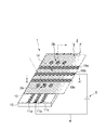
- FIG. 1 indicates a light-emitting device using the micro-channel device 2 of the present invention, and this light-emitting device 1 is connected to the micro-channel device 2 via wiring 4
- the power supply 5 is connected.
- a plurality of first electrodes 11a, 11b, 11c and a plurality of second electrodes 18a, 18b, 18c are provided in the microchannel device 2, and these first electrodes 11a, 11b, 11c and the second electrodes 18a, 18b, and 18c are individually provided with power via wiring.
- a common power supply 5 is connected to only one first electrode 11b and second electrode 18b via wiring 4, and the other first electrodes 11a, 11c and second electrodes are connected.
- the power supply connected to 18a and 18c is omitted.
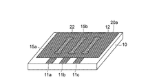
- the entire microchannel device 2 is formed in a flat shape, and a channel space 14 is formed therein.
- the width of the channel space 14 is selected to be about 10 to 2000 [ ⁇ m], the depth is about 10 to 200 [mm], and the thickness (distance between electrodes) is about 1 to 100 [ ⁇ m].
- a first substrate 7 provided with a plurality of first electrodes 11a, 11b, 11c and a second substrate 8 provided with a plurality of second electrodes 18a, 18b, 18c are joined.
- a hollow channel space 14 is formed between the first substrate 7 and the second substrate 8.
- the first substrate 7 has a configuration in which the channel forming layer 12 is provided on the support substrate 10, and the channel space 14 is formed in the channel forming layer 12.
- a flow path space 14 is surrounded by the support substrate 10, the flow path forming layer 12, and the second substrate 8.
- the microchannel device 2 is formed with a plurality of (in this case, three) channel spaces 14 having the same configuration, and a luminescent liquid is respectively contained in each channel space 14. It is configured to flow.
- a plurality of channel spaces 14 formed in a straight line are arranged so that the longitudinal directions thereof are parallel to each other.
- Each flow path space 14 has an inlet 2a formed at one end and an outlet 2b formed at the other end.
- tube members (not shown) are provided at the inlet 2a and the outlet 2b, respectively. Can be connected.
- the luminescent liquid is supplied to the channel space 14 from the inlet 2a at one end by the upstream tube member, the microchannel device 2 passes through the channel space 14 and flows at the other end.
- the luminescent liquid flows out from the outlet 2b to the tube member on the downstream side, and different luminescent liquids can flow into the respective flow path spaces 14.
- the luminescent liquid mentioned above refers to a form in which a luminescent compound is added to various solvents, liquid semiconductors, ionic liquids, or a mixed solution thereof.
- the light emitting compound is preferably a light emitter of an organic compound.
- the various solvents used are water, methanol, ethanol, 1-propanol, 2-propanol, tetrahydrofuran, 1,4-dioxane, acetone, 4-methyl-2-pentanone, acetylacetone, acetonitrile, propionitrile, ethylenediamine, pyridine.
- Formamide N-methylpyrrolidone, dimethyl sulfoxide, sulfolane, nitromethane, nitrobenzene, 1,2-dichlorobenzene, chloroform, methylene chloride, dichloromethane, 1,2-dichloroethane, propylene carbonate, ethylene carbonate, acetic acid, acetic anhydride, toluene, Examples include xylene, mesitylene, tetralin, decalin, n-butylbenzene, and benzonitrile.
- a liquid semiconductor refers to a state of a liquid organic semiconductor, for example, aromatic hydrocarbons such as a benzene derivative, a naphthalene derivative, an anthracene derivative, a carbazole derivative, and a typical one is 9- (2-ethylhexyl) carbazole (EHCz ) Or PLQ.
- the ionic liquid is an ionic liquid that is liquid at room temperature (25 ° C.), and a configuration represented by the general formula AB (A is a cation and B is an anion) is a good example.
- Examples of the cation represented by A above include the following. N, N, N-trimethylbutylammonium ion, N-ethyl-N, N-dimethylpropylammonium ion, N-ethyl-N, N-dimethylbutylammonium ion, N, N-dimethyl-N-propylbutylammonium ion, N- (2-methoxyethyl) -N, N-dimethylethylammonium ion, 1-ethyl-3-methylimidazolium ion, 1-ethyl-2,3-dimethylimidazolium ion, 1-ethyl-3,4- Dimethylimidazolium ion, 1-ethyl-2,3,4-trimethylimidazolium ion, 1-ethyl-2,3,5-trimethylimidazolium ion, N-methyl-N-propylpyrrolidinium ion, N
- N-methyl-N-propylpiperidinium ions are particularly preferred as the cation because of the wide potential window used.
- examples of the anion represented by B include PF 6 ⁇ , [PF 3 (C 2 F 5 ) 3 ] ⁇ , [PF 3 (CF 3 ) 3 ] ⁇ , BF 4 ⁇ , [BF 2 (CF 3) 2] -, [BF 2 (C 2 F 5) 2] -, [BF 3 (CF 3)] -, [BF 3 (C 2 F 5)] -, (BOB -), [(CF 3 SO 2 ) 2 N] ⁇ (TFSI ⁇ ), [(C 2 F 5 SO 2 ) 2 N] ⁇ (BETI ⁇ ), [(CF 3 SO 2 ) (C 4 F 9 SO 2 ) N] ⁇ , [ (CN) 2 N] ⁇ (DCA ⁇ ), [(CF 3 SO 2 ) 3 C] ⁇ , [(CN) 3 C] ⁇ and the anion
- BF 4 ⁇ [BF 3 (CF 3 )] ⁇ , [BF 3 (C 2 F 5 )] ⁇ , BOB ⁇ , TFSI ⁇ and BETI ⁇ are preferable.
- the addition amount of the luminescent substance is preferably 1 to 99% by weight, more preferably 5 to 90% by weight, with respect to various solvents, liquid semiconductors, ionic liquids or mixed solutions thereof.
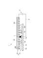
- FIG. 2A is a schematic diagram for explaining the light emission principle when a liquid semiconductor is used as the luminescent liquid L.
- FIG. 2A a voltage is applied to the first electrode 11b and the second electrode 18b by the power source 5, and in this state, the flow path between the first electrode 11b and the second electrode 18b.
- the luminescent liquid L flows into the space 14
- holes are injected from the first electrode 11b into the luminescent liquid L, and electrons are flown into the luminescent liquid L from the second electrode 18b.
- the holes and electrons in L recombine with each other, and the excitons generated thereby can emit light when returning to the ground state.
- FIG. 2B is a schematic diagram for explaining the light emission principle by the ECL.
- a voltage is applied to the first electrode 11b and the second electrode 18b by the power source 5, and the channel space 14 between the first electrode 11b and the second electrode 18b is applied.
- the cation radical R + generated at the first electrode 11b serving as the anode and the anion radical R ⁇ generated at the second electrode 18b serving as the cathode are contained in the luminescent liquid L. And neutral molecules in the ground state and excited state are generated, and the neutral molecules in the excited state can emit light when returning to the ground state.
- the luminescent liquid L constantly or intermittently flows in the flow path space 14 from the inlet 2a toward the outlet 2b, and the luminescent liquid L deteriorated in the flow path space 14.
- the new luminescent liquid L continues to be supplied to the flow path space 14 without being stopped, so that the optimum light emission state can be maintained for a long time.
- the second substrate 8 is disposed on the channel forming layer 12 of the first substrate 7, and the support substrate 10 and the channel forming layer 12 are sequentially arranged from the bottom.
- the second substrate 8 is laminated.
- the support substrate 10 constituting the first substrate 7 is made of various materials such as glass, polyester (PET (polyethylene terephthalate), PEN (polyethylene naphthalate)), polycarbonate, polyimide resin, acrylic resin member, and the like.
- the outer shape is formed in a plate shape or a sheet shape in a quadrilateral shape, and one surface on which the flow path forming layer 12 is laminated is formed flat.
- the light emitting state of the luminescent liquid L flowing in the channel space 14 is visually recognized from the outside on the first substrate 7 side by forming the support substrate 10 with various transparent materials. Can do.
- first electrodes 11a, 11b, and 11c are arranged on one surface of the support substrate 10 so as to run in parallel with each other in the longitudinal direction.
- the flow path forming layer 12 can be laminated so that the hole 15 faces the first electrodes 11a, 11b, and 11c.
- the first electrodes 11a, 11b, and 11c of the support substrate 10 are exposed in the groove forming through holes 15 of the flow path forming layer 12 on the first substrate 7, and the groove forming through holes 15 and the first electrodes 11a, 11a,
- a channel groove having a concave cross section can be formed by 11b and 11c.
- the first electrodes 11a, 11b, and 11c can be formed of a transparent electrode such as ITO, IZO, or ZnO, a metal such as gold, platinum, silver, magnesium, lithium, or aluminum, or an alloy thereof.
- the flow path forming layer 12 is formed of, for example, a negative photosensitive resin, and is formed so that a quadrilateral outline dimension is within the frame of the support substrate 10, and the longitudinal direction is substantially parallel to the longitudinal direction of the support substrate 10. Is provided.
- the flow path forming layer 12 is provided with circular diameter-enlarged regions 15a and 15b communicating with the inflow port 2a and the outflow port 2b, respectively, at both ends of the groove-forming through hole 15 formed in a band shape.
- the diameter-enlarged regions 15a and 15b can also be arranged to face the first electrodes 11a, 11b, and 11c on the support substrate 10.
- the first self-assembled monolayer 21a is selectively formed on the bonding surface 20a of the flow path forming layer 12 facing the second substrate 8 except for the flow path grooves. Is formed.
- the first substrate 7 has the second self formed on the bonding facing surface 20b of the second substrate 8 on the terminal functional group of the first self-assembled monolayer 21a on the bonding surface 20a facing the second substrate 8.
- the terminal functional group of the organized monolayer 21b is bonded, and the second substrate 8 can be bonded.
- the first self-assembled monolayer 21a is preferably composed of a self-assembled monomolecule having an epoxy as a terminal functional group.
- a self-assembled monomolecule having an epoxy as a terminal functional group For example, 3-glycidyloxypropyltrimethoxysilane (GOPTS, GPTS, GPTMS ), 3-glycidoxypropyltriethoxysilane (GPTES), 3-glycidoxypropylmethyldiethoxysilane (GPMDES), 3-glycidoxypropylmethyldimethoxysilane and the like.
- the second self-assembled monolayer 21b that binds to the terminal functional group of the first self-assembled monolayer 21a may be composed of a self-assembled monomolecule having —NH 2 as the terminal functional group.
- APTES 3-aminopropyltriethoxysilane
- APITMS 3-aminopropyltrimethoxysilane
- N-2- (aminoethyl) -3-aminopropylmethyldimethoxysilane N-2- (aminoethyl) -3-aminopropyltrimethoxysilane
- N-2- (aminoethyl) -3-aminopropyltriethoxysilane N-2- (aminoethyl) -3-aminopropyltriethoxysilane, and the like.
- a self-assembled monomolecular film having epoxy as a terminal functional group is formed on the first substrate 7 as the first self-assembled monomolecular film 21a, and —NH 2 is formed as the terminal functional group.
- the present invention is not limited to this.
- a self-assembled monomolecular film having a second self-assembled monomolecular film on the second substrate 8 and a self-assembled monomolecular film having —NH 2 as a terminal functional group as the first self-assembled monomolecular film May be formed on the first substrate 7.
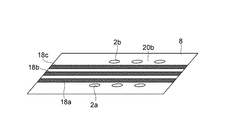
- the second substrate 8 on which such second self-assembled monolayer 21b is formed is, for example, polyester (PET (polyethylene terephthalate) or PEN (polyethylene naphthalate)), polycarbonate, polyimide resin, acrylic resin member. It is made of various film-like or sheet-like materials, and its outer shape is formed in a quadrilateral shape, and a joining facing surface 20b joined to the joining surface 20a of the first substrate 7 is formed almost flat.
- the second substrate 8 is formed of various transparent materials, so that the light emission state of the luminescent liquid L flowing in the channel space 14 can be changed from the outside on the second substrate 8 side. Visible.
- a plurality of strip-shaped second electrodes 18a, 18b, 18c are arranged on the joint facing surface 20b of the second substrate 8 so as to run in parallel in the longitudinal direction. These second electrodes 18a, 18b, 18c
- the first substrate 7 may be disposed so that the longitudinal direction of the first substrate 7 is orthogonal to the longitudinal direction of the flow channel grooves of the first substrate 7 (that is, the first electrodes 11a, 11b, 11c).
- a channel space 14 in which, for example, the first electrode 11b and a part of the second electrode 18b face each other can be formed between the first substrate 7 and the second substrate 8.
- the second electrodes 18a, 18b, and 18c are made of, for example, transparent electrodes such as ITO, IZO, and ZnO, as well as the first electrodes 11a, 11b, and 11c, as well as gold, platinum, silver, magnesium, lithium, and aluminum.
- the second substrate 8 is provided with a plurality of inlets 2a and outlets 2b penetrating the thickness at predetermined positions around the second electrodes 18a, 18b, 18c.
- the second substrate 8 is positioned on the flow path forming layer 12 so that the inlet 2a and the outlet 2b overlap with the enlarged diameter regions 15a and 15b of the flow path forming layer 12, and is joined to the flow path forming layer 12. obtain.
- the support substrate 10 and the second substrate are formed of a soft member such as polyester (PET), and the first electrodes 11a, 11b, 11c and the second electrodes 18a, 18b,
- a soft electrode member such as ITO
- ITO a soft electrode member such as ITO
- the longitudinal direction of the second electrodes 18a, 18b, 18c on the second substrate 8 is the longitudinal direction of the first electrodes 11a, 11b, 11c on the first substrate 7.
- the one end of the first substrate 7 protrudes from the side of the second substrate 8 and the one end of the second substrate 8 protrudes from the side of the first substrate 7. It has a configuration.
- the microchannel device 2 can expose the first electrodes 11a, 11b, 11c at one end of the first substrate 7 without overlapping the second substrate 8, and accordingly, the first electrodes 11a, 11b. , 11c can be easily connected to the wiring 4.
- the wiring 4 is connected to the second electrodes 18a, 18b, and 18c accordingly. It can be easily connected.
- the micro-channel device 2 having such a configuration is selected only for the joining surface 20a except for the channel groove of the first substrate 7, as shown in FIG. 4 showing a side cross-sectional configuration of the AA ′ portion of FIG.
- Terminal functional groups of the first self-assembled monolayer formed on the second substrate 8 and the second self-assembled monolayer on the bonding facing surface 20b of the second substrate 8 are bonded to each other.
- the substrate 8 is joined, the channel groove is not bonded to the second substrate 8, the hollow channel space 14 can be reliably formed, and the characteristics of the channel space are not changed.
- the characteristics of the first electrode 11a, 11b, 11c, the flow path forming layer 12, the second electrode 18a, 18b, 18c, and the second substrate 8 can be maintained.
- the luminescent liquid L can be surely passed through the channel space 14, and the first electrode 11a, 11b, 11c and the second electrode 18a, 18b, 18c are supplied by the power source 5.
- the luminescent liquid L flowing through the flow path space 14 can be caused to emit light.
- a manufacturing method of such a microchannel device 2 will be described below.
- a plate-like support substrate having an electrode layer formed on the surface is prepared, and the electrode layer on the support substrate is etched with a resin mask pattern, and as shown in FIG. Shaped first electrodes 11a, 11b, and 11c are formed.
- a negative photosensitive resin is spin-coated on the support substrate 10 on which the first electrodes 11a, 11b, and 11c are formed, and the negative photosensitive resin is heated and prebaked.
- a belt-shaped groove-forming through-hole region 22 having enlarged diameter regions 15a and 15b at both ends can be exposed using a mask (not shown) using an exposure apparatus for performing photolithography. Solubilize.
- post-exposure baking is performed at a predetermined temperature, development is performed with a developer, and the solubilized groove-forming through-hole region 22 is removed to form the groove-forming through-hole 15 in the negative photosensitive resin.
- Post-baking is performed at a temperature, and a flow path forming layer 12 in which the first electrodes 11a, 11b, and 11c are exposed at the bottom of the groove forming through hole 15 is formed on the support substrate 10 (not shown).
- the flow path forming layer 12 is preferably formed of the above-described negative photosensitive resin since it is desired that the height and width of the flow path groove can be easily changed.
- SU manufactured by Microchem (Nippon Kayaku) -8 series, KMPR series, Tokyo Ohka Kogyo TMMR S2000, Toray Photo Nice (photosensitive polyimide), etc. are used.
- a dummy member such as a dummy resin (TSMR: manufactured by Tokyo Ohka Kogyo Co., Ltd.) is prepared, and the dummy member 23a is formed in the groove forming through hole 15 of the flow path forming layer 12 as shown in FIG. And then baked at a predetermined temperature. In this way, the entire inside of the channel groove 23 is covered with the dummy member 23a, and the first electrodes 11a, 11b, 11c in the channel groove 23 are not exposed to the outside.
- TSMR dummy resin
- the dummy member 23a for example, the TSMR series manufactured by Tokyo Ohka Kogyo, which is a positive resist that dissolves in an organic solvent (acetone or the like), the OFPR series, the AZ series manufactured by Clariant, or the like may be used.
- the dummy member 23a when the channel groove width is 500 [un] or larger, the dummy member 23a may be provided directly in the channel groove by directly tracing the dummy member 23a with a syringe or the like.
- the dummy member 23a when the flow path width is narrow, after the dummy member 23a is spin-coated on the substrate 10, the dummy member 23a is formed by exposing and developing a portion other than the portion where the dummy member is to be formed using a mask.
- the flow channel groove is covered with a plate-like member provided with a supply port and a discharge port, and the dummy member 23a is fed from the supply port through the flow channel groove to the dummy member 23a.
- the member 23a may be provided, and then the plate member may be removed to form the dummy member 23a only in the flow channel.
- a film-like second substrate having an electrode layer formed on the surface is prepared, and the electrode layer on the second substrate is etched with a resin mask pattern, and as shown in FIG.
- Second electrodes 18a, 18b and 18c having a predetermined shape are formed on the two substrates 8 from electrode layers.
- the second substrate 8 has through-holes having substantially the same shape and size as the enlarged diameter regions 15a and 15b at positions corresponding to the enlarged diameter regions 15a and 15b of the groove-forming through-holes 15 of the flow path forming layer 12.
- a hole is formed by punching to form an inlet 2a and an outlet 2b.
- the second substrate 8 is manufactured in which the second electrodes 18a, 18b, and 18c are provided on the bonding facing surface 20b, and the inflow port 2a and the outflow port 2b are formed.
- the excimer UV is applied to the bonding surface 20a provided with the dummy member 23a of the first substrate 7 and the bonding facing surface 20b provided with the second electrode 18b of the second substrate 8.
- the lamp is irradiated with vacuum ultraviolet light (VUV / O 3 ), and oxygen-containing groups (carboxyl groups, ketones) are formed on the dummy member 23a and the bonding surface 20a of the first substrate 7 and the bonding facing surface 20b of the second substrate 8, respectively.
- oxygen-containing groups carboxyl groups, ketones
- UV / O 3 treatment using a low-pressure mercury lamp, atmospheric pressure plasma treatment, Vacuum plasma treatment or the like may be used.
- first substrate is immersed in a first self-assembled monomolecular formation solution (first SAM formation solution), and as shown in FIG. 10A, on the bonding surface 20a of the first substrate 7 and the dummy member 23a, For example, a first self-assembled monolayer 21a having a terminal functional group made of epoxy such as 3-glycidyloxypropyltrimethoxysilane (GOPTS) is formed.
- first substrate 7 is rinsed with a removing solution such as acetone, and the residual self-assembled monomolecules that are not attached to the bonding surface 20a and the dummy member 23a in the channel groove 23 are removed.
- a removing solution such as acetone
- the first electrode 11a, 11b, 11c is exposed on the bottom of the flow channel 23 on the first substrate 7, and the first self-organization is selectively performed only on the bonding surface 20a excluding the flow channel 23.
- a monomolecular film 21a can be formed.
- the second substrate 8 is immersed in a second self-assembled monomolecular formation solution (second SAM formation solution), and as shown in FIG. 10B, on the bonding facing surface 20b of the second substrate 8, for example, 3- A second self-assembled monolayer 21b whose terminal functional group is an amino group, such as aminopropyltriethoxysilane (APTES), is formed.
- second substrate 8 is rinsed with ethanol or the like to remove residual self-assembled monomolecules that are not attached to the bonding facing surface 20b.
- the second substrate 8 includes the second self-assembled monomolecule on the entire bonding facing surface 20b other than the second electrodes 18a, 18b, 18c, including the exposed second electrodes 18a, 18b, 18c.
- the film 21b can be formed.
- the first substrate 7 whose surface 20a is modified by the first self-assembled monolayer 21a and the second surface 20b whose surface 20b is modified by the second self-assembled monolayer 21b.
- the substrate 8 is brought into contact, and the first substrate 7 and the second substrate 8 are loaded and heated in this state, and as shown in FIG. 11, the terminal functional groups of the first self-assembled monolayer 21a and the first functional group 2
- the terminal functional group of the self-assembled monomolecular film 21b is bonded by an epoxy-amino reaction.
- the first self-assembled monolayer 21a is formed. Since the entire flow channel groove 23 that was not formed was white, it was confirmed that the hollow flow channel space 14 could be reliably formed without the entire flow channel groove 23 being bonded to the second substrate 8. .
- the second substrate 8 has a slightly concavity and convexity on the bonding facing surface 20b on which the second electrodes 18a, 18b, and 18c are provided depending on the presence or absence of the second electrodes 18a, 18b, and 18c.
- the first self-assembled monolayer 21a of the first substrate 7 and the second self-assembled monolayer 21b of the bonding facing surface 20b are formed of a deformable film-like member. Therefore, the bonding facing surface 20b is brought into close contact with the bonding surface 20a of the first substrate 7 so that the bonding can be reliably performed.
- the first substrate 7 and the second substrate 8 are closely bonded without forming a gap, and the channel space 14 that communicates with the outside only through the inlet 2 a and the outlet 2 b is formed.
- the first substrate 7 and the second substrate 8 can be formed.
- the microchannel device 2 was actually manufactured according to the above manufacturing method, and a light-emitting device 1 using this micro-channel device 2 In FIG. 5, the verification was made on how the luminescent liquid L emits light in the flow path space.
- the microchannel device 2 was manufactured as follows. First, an ITO-glass substrate was prepared in which a supporting substrate 10 was a 700 [ ⁇ m] thick glass substrate on which 100 [nm] thick ITO was formed on one surface. Next, a resin mask pattern was formed on the ITO using a positive photosensitive resin TSMR manufactured by Tokyo Ohka Kogyo Co., Ltd.
- the support substrate 10 formed so that the three first electrodes 11a, 11b, and 11c having a strip shape as shown in FIG.
- a negative photosensitive resin (SU-8 3005: manufactured by Nippon Kayaku Co., Ltd.) with excellent chemical resistance and mechanical properties is spin-coated to a thickness of 6 [ ⁇ m], and this negative photosensitive resin is hot.
- a mask aligner MA6: manufactured by Carlsose
- the exposure was carried out at [mW / cm 2 ] for 6 seconds to solubilize the groove-forming through-hole region 22 as shown in FIG.
- the flow path forming layer 12 with the first electrodes 11a, 11b, and 11c exposed at the bottom of the groove forming through hole 15 is further hard-baked at 150 [° C.]. It was formed on the support substrate 10.
- a resin material made of TSMR (manufactured by Tokyo Ohka Kogyo Co., Ltd.) is prepared as a dummy member 23a, and as shown in FIG. 7, this TSMR is injected into the groove forming through-hole 15 of the flow path forming layer 12, and hot The plate was baked at 110 [° C.] for 5 minutes. In this way, the entire inside of the channel groove 23 is covered with the dummy member 23a, and the first electrodes 11a, 11b, 11c in the channel groove 23 are not exposed to the outside. In this state, vacuum ultraviolet light ( VUV / O 3 ) was irradiated to form oxygen-containing groups on the flow path forming layer 12 and the dummy member 23a.
- VUV / O 3 vacuum ultraviolet light
- first SAM formation solution a 1% (v / v) 3-glycidyloxypropyltrimethoxysilane (GOPTS) solution dissolved in pure water is prepared as a first self-assembled monomolecular formation solution (first SAM formation solution) to form a first SAM.
- first SAM formation solution a first self-assembled monomolecular formation solution
- the first substrate 7 is immersed in the solution for 20 minutes, and a first self-assembled monolayer 21a in which GOPTS having a terminal functional group made of epoxy is provided on the bonding surface 20a of the first substrate 7 and the dummy member 23a as a film. Formed.
- the first substrate 7 is rinsed with acetone to cover the remaining self-assembled monomolecules not attached to the bonding surface 20a and the flow channel 23.
- the dummy member 23a was removed, and then rinsed with isopropyl alcohol and pure water to remove acetone.
- the first electrodes 11a, 11b, 11c are exposed at the bottom of the flow channel 23, and the first self-assembled monolayer 21a is selectively formed only on the bonding surface 20a excluding the flow channel 23.
- a first substrate 7 was manufactured.
- an ITO-PEN film in which ITO having a thickness of 350 [nm] was formed on a PEN film having a thickness of 120 [ ⁇ m] was prepared as the second substrate 8.
- the ITO on the second substrate 8 was etched with a resin mask pattern, and as shown in FIG. 8, three second electrodes 18a, 18b, 18c having a strip shape were formed from the ITO.
- a through hole having substantially the same shape and size as the enlarged diameter regions 15 a, 15 b is provided at a position corresponding to the enlarged diameter regions 15 a, 15 b of the groove forming through hole 15 in the flow path forming layer 12. Were punched to form the inlet 2a and the outlet 2b.
- the second substrate 8 in which the second electrodes 18a, 18b, and 18c were provided on the bonding facing surface 20b and the inflow port 2a and the outflow port 2b were formed was manufactured.
- the junction facing surface 20b of the second substrate 8 was also irradiated with vacuum ultraviolet light (VUV / O 3 ) by an excimer UV lamp to form an oxygen-containing group on the junction facing surface 20b.
- VUV / O 3 vacuum ultraviolet light
- APTES 3-aminopropyltriethoxysilane
- second SAM formation solution a second self-assembled monomolecular formation solution
- the second substrate 8 was immersed in the solution for 20 minutes to form a second self-assembled monolayer 21b in which the APTES whose terminal functional group is an amino group was provided on the bonding facing surface 20b of the second substrate 8 as a film.
- the second substrate 8 is lifted from the second SAM forming solution, the second substrate 8 is rinsed with ethanol to remove residual self-assembled monomolecules not attached to the bonding facing surface 20b, and thus exposed.
- a second substrate 8 was produced in which the second self-assembled monolayer 21b was formed on the bonding facing surface 20b including the second electrodes 18a, 18b and 18c.
- first self-assembled monolayer 21a of the first substrate 7 and the second self-assembled monolayer 21b of the second substrate 8 are brought into contact with each other, and the bonding apparatus (EVG520HE: EV group, Inc.) remains in this state.
- the first self-assembled monolayer 21a and the second self-assembled monolayer 21b are bonded to each other by applying a load with a load of 1.5 [MPa], a temperature of 140 [° C] and a holding time of 5 minutes.
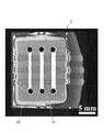
- the substrate 7 and the second substrate 8 were joined, and the microchannel device 2 including the three channel spaces 14 having widths of 1000 [ ⁇ m], 1250 [ ⁇ m], and 1500 [ ⁇ m] was manufactured.
- the fixing device 41 includes a first plastic plate 52 erected on a base 51 and a second plastic plate 53 that is a separate body from the first plastic plate 52.
- the micro-channel device 2 was made visible through the glass windows 57 and 58 embedded in the first plastic plate 52 and the second plastic plate 53 with the device 2 interposed therebetween.
- the first plastic plate 52 is provided with a pin member 55a penetrating the thickness, and one end of the pin member 55a exposed on one surface is brought into contact with the second electrodes 18a, 18b, 18c of the microchannel device 2 and exposed on the other surface.
- the wiring 4 (FIG. 13) is connected to the other end of the pin member 55a so that the voltage from the power supply device 43 can be applied to the second electrodes 18a, 18b, and 18c via the wiring 4 and the pin member 55a.
- the second plastic plate 53 is provided with a pin member 55b penetrating the thickness, and one end of the pin member 55b exposed on one surface is brought into contact with the first electrodes 11a, 11b, 11c of the microchannel device 2, and the other surface
- the wiring 4 (FIG. 13) is connected to the other end of the pin member 55b exposed to the voltage so that the voltage from the power supply device 43 can be applied to the first electrodes 11a, 11b, and 11c via the wiring 4 and the pin member 55b. did.
- the second plastic plate 53 is provided with openings communicating with the inlet 2a and the outlet 2b of the microchannel device 2, and a sealing pin 56 or a connecting pipe 56a (FIG. 13) is provided in the opening. It was.
- the cylinder 44 is connected to the inlet 2a communicating with the channel space 14 to be verified in the microchannel device 2 via the connection pipe 56a, and the cylinder 44 is connected to the inlet 2a via the inlet 2a.
- the luminescent liquid L was supplied to the channel space 14. Note that the luminescent liquid L supplied to the flow path space 14 is retained in the flow path space 14 by the sealing pin 56 provided at the outlet 2b of the micro flow path device 2.
- UV is irradiated to the microchannel device 2 using the UV lamp 45, and the light emission state of the luminescent liquid L supplied into the channel space 14 of the microchannel device 2 is imaged by the digital camera 46.
- a liquid semiconductor is injected as the luminescent liquid L into the channel space 14 located in the center among the three channel spaces 14 of the microchannel device 2 to correspond to the channel space 14.
- a voltage was applied to the central first electrode 11b and the three second electrodes 18a, 18b, 18c orthogonal to the first electrode 11b. As a result, a result as shown in FIG. 15A was obtained.
- the microfluidic device 2 manufactured by the manufacturing method described above, the first electrode 11b and the second electrodes 18a, 18b, at 18c is opposed, centrally disposed hollow flow path space 14b 1 It was confirmed that the luminescent liquid L emitted light. In addition, it was confirmed that in the flow path space 14b 1 , it was possible to prevent defects due to the joining of the flow path grooves of the first substrate 7 and the second substrate 8.
- rubrene ((5,6,11,12) -tetraphenyltetracene) that emits yellow light is mixed into a mixed solvent (2: 1, v / v) of 1,2 dichlorobenzene and acetonitrile.
- DBP Dissolved luminescent solution
- DBP-rubrene solution Dissolved luminescent solution
- a luminescent compound doped with rubrene mixed solvent of 1,2 dichlorobenzene and acetonitrile (2: 1, v / v )
- a luminescent solution hereinafter simply referred to as a DBP-rubrene solution
- the rubrene solution is allowed to flow through the channel space 14a 1 on one end side and the DBP-rubrene in the channel space 14c 1 on the other end side
- the solution was allowed to flow, and voltages were applied to the three second electrodes 18a, 18b, 18c orthogonal to the first electrode 11b.
- FIG. 15B a result as shown in FIG. 15B was obtained.
- the hollow channel space 14a 1 arranged on one end side is turned yellow by a rubden solution (indicated simply as “rubrene” in FIG. 15B).
- the hollow channel space 14c 1 arranged on the other end side can be made to emit red light with a DBP-rubrene solution (indicated simply as “DBP” in FIG. 15B). did it.
- DBP DBP-rubrene solution
- DPA 9,10-diphenylanthracene
- a luminescent solution dissolved in v) (hereinafter simply referred to as a DPA solution) is prepared, and this DPA solution is allowed to flow only in the central flow path space 14b 1 and three second electrodes 18a, Voltage was applied to 18b and 18c.
- a result as shown in FIG. 15C was obtained. From FIG. 15C, in the microchannel device 2 manufactured by the above-described manufacturing method, the blue channel space 14b 1 disposed in the center emits blue light by the DPA solution (simply expressed as “DPA” in FIG. 15C). I was able to.
- the concentration of rubrene in the rubrene solution is preferably 1 to 20 [mM], and the concentrations of rubrene and DBP used in the DBP-rubrene solution are preferably 1 to 20 [mM] and 0.1 to 0.4 [mM], respectively.
- the concentration of DPA is preferably 5 to 50 [mM].
- non-patent literature "K. Nishimura etal., Solution Electrochemiluminescent Cell with a High Luminance Using an Ion Conductive Assistant Dopant '', Japanese Journal of Applied Physics (Jpn. J. Appl. Phys), vol. pp. L 1323-L 1326, .2001 ”is added to the luminescent liquid as an ion conductive auxiliary dopant (0.122M of 1,2 diphenoxyethane).
- the luminescent liquid L is changed, and the rubrene solution that emits yellow light again as the luminescent liquid L is caused to flow through the channel space 14a 1 on one end side and the channel space 14c 1 on the other end side, and the first electrode.
- a voltage was applied to the three second electrodes 18a, 18b, and 18c orthogonal to 11b.
- FIG. 15D a result as shown in FIG. 15D was obtained.
- the rubrene solution is passed through the hollow channel space 14a 1 disposed on one end side and the hollow channel space 14c 1 disposed on the other end side.
- each channel space 14a 1 to 14c 1 can simultaneously emit yellow light, and even if the luminescent liquid L is changed, each channel space 14a 1 to 14c 1 emits light without causing poor bonding. I was able to.
- each channel space 14a 1 to 14c 1 can be caused to emit light using not only a liquid semiconductor but also various luminescent liquids L, and light emission It was confirmed that each flow path space 14a 1 to 14c 1 can emit light even when the type of the ionic liquid L is changed.
- the first self-assembled monolayer 21a is selectively formed only on the bonding surface 20a excluding the channel groove 23 of the first substrate 7. Then, the terminal functional group of the second self-assembled monolayer 21b formed on the bonding facing surface 20b of the second substrate 8 and the terminal functional group of the first self-assembled monolayer 21a are bonded to each other. The first substrate 7 and the second substrate 8 are joined together to form a hollow flow path space 14 between the first substrate 7 and the second substrate 8.
- the first self-assembled monolayer 21a is not formed in the channel groove 23 since the first self-assembled monolayer 21a is not formed in the channel groove 23, characteristics such as wettability, surface free energy, surface functional groups, etc. of the channel groove 23 are obtained.
- the characteristics of the material of the flow channel 23 itself can be maintained without change, and the first substrate can be reliably bonded to the second substrate 8 only by the bonding surface 20a excluding the flow channel 23. It is possible to prevent defects caused by joining the seven flow path grooves and the second substrate 8.
- the first electrodes 11a, 11b, and 11c are formed so as to be exposed in the channel groove 23, and the first electrodes 11a, 11b, and 11b are formed on the bonding facing surface 20b of the second substrate 8.
- Second electrodes 18a, 18b, 18c that are at least partially opposed to 11c are provided, and these first electrodes 11a, 11b, 11c and second electrodes 18a, 18b, 18c are arranged to face each other across channel space 14 I tried to do it.
- the microchannel device 2 by applying a voltage to the first electrodes 11a, 11b, 11c and the second electrodes 18a, 18b, 18c, the first electrodes 11a, 11b, 11c and the second electrodes 18a, the first electrodes 11a, 11b, 11c and the second electrodes 18a, The luminescent liquid L flowing in the flow path space 14 between 18b and 18c can emit light.
- the luminescent liquid L can be supplied from the inflow port 2a to the channel space 14 by providing the inflow port 2a and the outflow port 2b for communicating the channel space 14 with the outside.
- the luminescent liquid L supplied to the flow path space 14 can flow out from the outlet 2b, so that the deteriorated luminescent liquid L does not stay in the flow path space 14, and a new luminescent liquid L is always flowed.
- the luminescent liquid L can continue to emit light in the space 14 by being given in the space 14.
- first electrodes 11a, 11b, 11c and second electrodes 18a, 18b, 18c are provided, and these first electrodes 11a, 11b, 11c and second electrodes 18a, 18a, Since 18b and 18c are arranged in a matrix, the first electrode 11a, 11b and 11c and the second electrode 18a, 18b and 18c to which the voltage is applied by the power source 5 are selected, so that the current to which the voltage is applied is selected. Only the luminescent liquid L flowing through the road space 14 can emit light.
- the present invention is not limited to this embodiment, and various modifications can be made within the scope of the gist of the present invention.
- the present invention is not limited to this, and as shown in FIG.
- Light-emitting device using a micro-channel device 62 provided with a merged channel space 14e, 14g in which a plurality of channel spaces 14b, 14c, 14d merge in addition to the channel spaces 14a, 14c, 14d and the curved channel space 14b 61 may be produced.
- the microchannel device 62 includes, for example, four inlets 63a, 63b, 63c, and 63d and three outlets 64a, 64b, and 64c, of which a pair of inlets 63a and outlets are formed.
- a straight channel space 14a is provided between 64a.
- the other inlet 63b and outlet 64b there are a plurality of U-shaped curved portions that are continuous and folded to the left and right, and a branch channel space 14f branched from the adjacent merge channel space 14e.
- a flow path space 14b and a merged flow path space 14g joined together are provided.
- microchannel device 62 different syringes 44a, 44b, 44c, 44d are connected to the respective inlets 63a, 63b, 63c, 63d, and are different from the respective syringes 44a, 44b, 44c, 44d.
- a luminescent liquid can be supplied.
- the microchannel device 62 is provided with a plurality of first electrodes and second electrodes (not shown), and channel spaces 14a, 14b, 14c, 14d are provided between the first electrodes and the second electrodes.
- the confluence channel spaces 14e, 14g are arranged, and by applying a voltage to the first electrode and the second electrode, the channel spaces 14a, 14b, 14c, between the first electrode and the second electrode to which the voltage is applied.
- the luminescent liquid flowing in 14d or the merged flow path spaces 14e and 14g can emit light.
- a plurality of types of luminescent liquids can be mixed in the merged channel spaces 14e and 14g, and thus the luminescent liquids can be mixed while emitting light in the luminescent color of the luminescent liquid alone.
- the combined flow path spaces 14e and 14g can be continuously emitted with a new emission color in which the emission colors are mixed.
- the microchannel device 62 having such a configuration can be manufactured in accordance with the above-described “(2) Manufacturing method of microchannel device”. Specifically, a channel groove having a complicated shape may be formed in the channel forming layer in accordance with the shape of the channel spaces 14a, 14b, 14c, 14d and the merged channel spaces 14e, 14g. Then, a dummy member is provided in the flow channel groove, and the first self-assembled monolayer is formed in this state, and then the dummy member is removed, so that only the bonding surface excluding the flow channel groove is the first. A self-assembled monolayer can be formed.
- a second substrate having a second self-assembled monolayer formed on the bonding facing surface is prepared, and the first self-assembled monolayer of the first substrate and the second self-assembled monolayer of the second substrate are prepared.
- the microchannel device 62 can be manufactured by bonding the first substrate and the second substrate.
- the first electrode 11a, 11b, 11c and the second electrode 18a, 18b, 18c are provided in the flow path space 14 between the first substrate 7 and the second substrate 8.
- the present invention is not limited to this, and the first electrode 11a, 11b, 11c and the second electrode 18a, 18b , 18c may be used, and a microchannel device that simply includes a hollow channel space 14 between the first substrate 7 and the second substrate 8 may be applied.
- the present invention is not limited to this, and the second substrate The second self-assembled monolayer 21b may be formed only on the bonding facing surface 20b excluding the region facing the flow channel 23 out of the eight bonding facing surfaces 20b.
- the first substrate 7, not only the channel groove 23 of 7 but also the bonding facing surface 20 b of the second substrate 8 located in the channel space 14 is not subjected to surface modification.
- the characteristics of the materials of the first electrodes 11a, 11b, 11c, the flow path forming layer 12, the second electrodes 18a, 18b, 18c, and the second substrate 8 are maintained without changing the characteristics such as free energy and surface functional groups.
- the second substrate 8 can be reliably bonded to the bonding surface 20a excluding the flow channel groove 23 while being maintained in the flow channel space 14. Runode may prevent failure due to bonding of the flow channel and the second substrate 8 of the first substrate 7.
- the light-emitting device using the micro-channel device of the present invention can emit a single-color or multi-color luminescent solution within the channel path of the micro-channel device formed on one chip. Therefore, it can be used as, for example, a full color display or illumination.
- the light emitting device can also be used as a micron-scale light source for irradiating excitation light in a fluorescence detection sensor or the like. That is, in this case, in the light emitting device, in the microchannel device, the luminescent solution is selected by the channel path 14 formed in the micron-scale width, and various lights in the visible light region (350 to 850 nm) are emitted. Therefore, it can be used as an excitation light source for measuring the fluorescence amount of the target sample in a specific wavelength region.
- the microchannel device of the present invention can reliably produce a hollow channel space having a desired shape and a micro size, for example, when analyzing various fluids such as liquid and gas in an analyzer, It can also be used as a device for confining a fluid in a channel space or flowing in a channel space. That is, in this case, in the microchannel device of the present invention, for example, a minute reaction chamber or mixing chamber provided on the substrate as one type of channel space, a channel, and other various blood or DNA to be analyzed Since it is possible to flow a biological sample made of liquid or gas, it can also be used as a micro TAS (Total Analysis System) for analyzing these liquids and gases and as a flow channel device used for immunoassay.
- TAS Total Analysis System
Abstract
Proposed are a microchannel device (2) capable of maintaining desired characteristics in a channel space (14) and preventing a failure due to joining of a channel groove (23) in a first substrate (7) and a second substrate (8), and a method for manufacturing the same. Since a first self-assembled monomolecular film (21a) is not formed in the channel groove in the microchannel device, the characteristics of the materials themselves of first electrodes (11a, 11b, 11c) and a channel formation layer (12) can be maintained in the channel space without change in characteristics such as wettability, surface free energy, and a surface functional group in the channel groove, and joining with the second substrate can be reliably performed by only a joint surface (20a) except the channel groove, thereby making it possible to prevent the failure due to joining of the channel groove in the first substrate and the second substrate.
Description
本発明は、マイクロ流路デバイス及びその製造方法に関し、例えば第1基板と第2基板との間に中空の流路空間を備えるマイクロ流路デバイスに適用して好適なものである。
The present invention relates to a microchannel device and a method for manufacturing the microchannel device, and is suitable for application to, for example, a microchannel device having a hollow channel space between a first substrate and a second substrate.
近年、半導体微細加工技術を利用し、機械的機能と電気的機能とを備えたマイクロデバイスを作製するMEMS(Micro Electro Mechanical Systems)の研究が注目されている。このようなMEMS技術を応用したものとして、流路や、ポンプ、バルブ、ミキサ等の微小構造体を数センチ角の基板上に集積化し、流体の送液や、混合等を行って流体を分析するμTAS(Micro Total Analysis Systems)が知られている。さらに、近年ではデバイスの高機能化に向けて、流路空間内に電極を設けた電極埋め込み型のマイクロ流路デバイスも考えられており、この種の電極埋め込み型のマイクロ流路デバイスの製造方法についても研究が進められている。ここで、従来のマイクロ流路デバイスの製造方法としては、例えば流路やチャンバとなる凹み状の溝が形成された凹基板と、平板状のカバー基板とを接合してマイクロ流路デバイスを製造する製造方法が知られている。
Recently, research on MEMS (Micro Electro Mechanical Systems) that produces micro devices with mechanical and electrical functions using semiconductor microfabrication technology has attracted attention. As an application of such MEMS technology, flow structures, pumps, valves, mixers, and other microstructures are integrated on several centimeter square substrates, and fluids are sent and mixed to analyze fluids. ΜTAS (Micro Total Analysis Systems) is known. Furthermore, in recent years, an electrode-embedded microchannel device in which an electrode is provided in the channel space is also being considered for higher functionality of the device, and a method for manufacturing this type of electrode-embedded microchannel device Research is also underway. Here, as a conventional method of manufacturing a microchannel device, for example, a microchannel device is manufactured by joining a concave substrate formed with a concave groove to be a channel or a chamber and a flat cover substrate. Manufacturing methods are known.
このような第1基板としての凹基板と、第2基板としてのカバー基板との接合方法としては、例えば凹基板及びカバー基板に、真空プラズマや、エキシマUVランプによる真空紫外線を照射することによって、これら凹基板及びカバー基板の各接合面に酸素含有基を導入し、それら接合面を貼り合わせて熱圧着させることで、酸素含有基同士を反応させて接合する製造方法が知られている(例えば、特許文献1及び非特許文献1参照)。なお、酸素含有基導入による接合方法としては、上述した手法だけに限らず、例えば低圧水銀ランプによるUVオゾン処理や、大気圧プラズマ処理などを用いても良い。さらに、その他の接合方法としては、非特許文献2に示すように、自己組織化単分子膜(SAM膜)を凹基板及びカバー基板に形成し、自己組織化単分子膜の末端官能基同士を化学反応させて結合させ、これら凹基板及びカバー基板を接合する接合方法も知られている。
As a method for joining such a concave substrate as the first substrate and a cover substrate as the second substrate, for example, the concave substrate and the cover substrate are irradiated with vacuum plasma or vacuum ultraviolet rays by an excimer UV lamp, A manufacturing method is known in which oxygen-containing groups are introduced into each bonding surface of the concave substrate and the cover substrate, and the bonding surfaces are bonded and thermocompression bonded together to react and bond oxygen-containing groups (for example, Patent Document 1 and Non-Patent Document 1). Note that the bonding method by introducing the oxygen-containing group is not limited to the above-described method, and for example, UV ozone treatment using a low-pressure mercury lamp, atmospheric pressure plasma treatment, or the like may be used. Furthermore, as another bonding method, as shown in Non-Patent Document 2, a self-assembled monomolecular film (SAM film) is formed on a concave substrate and a cover substrate, and terminal functional groups of the self-assembled monomolecular film are bonded to each other. A bonding method is also known in which the concave substrate and the cover substrate are bonded by chemical reaction.
しかしながら、前者の酸素含有基導入による接合方法や、後者の自己組織化単分子膜を用いた接合方法では、凹基板及びカバー基板の接合面だけではなく、流路空間となる流路溝表面にまで表面改質が行われてしまうことから、流路溝表面が凹基板及びカバー基板自体の材質と異なる濡れ性や官能基を有してしまい、改めて流路空間内の特性の調整が必要となる場合があるという問題あった。
However, in the former joining method by introducing an oxygen-containing group and the latter joining method using a self-assembled monolayer, not only on the joint surface of the concave substrate and the cover substrate, but also on the surface of the channel groove serving as the channel space. Since the surface modification is performed until the surface of the channel groove has wettability and functional groups different from the material of the concave substrate and the cover substrate itself, it is necessary to adjust the characteristics in the channel space again. There was a problem that sometimes.
また、このようなマイクロ流路デバイスでは、微細構造でなることから、特にアスペクト比が低い流路溝の場合、凹基板及びカバー基板を密着させ荷重を加えて接合させる際、この荷重によって凹基板やカバー基板が変形して流路溝の一部とカバー基板とが接触し、その結果、流路溝及びカバー基板の表面官能基同士が反応してしまい、凹基板の流路溝とカバー基板とが接合されてしまう不良が生じ、所望の流路空間を形成できない等の不良が生じる虞がある。さらに、上述した電極埋め込み型のマイクロ流路デバイスでは、例えば自己組織化単分子膜を用いることで電極表面の仕事関数等の特性にも影響が生じる虞があることから、これら予測不可能な不良が生じることも考えられる。
Further, in such a microchannel device, since it has a fine structure, particularly in the case of a channel groove having a low aspect ratio, when the concave substrate and the cover substrate are brought into close contact with each other and applied with a load, the concave substrate is caused by this load. The cover substrate is deformed and a part of the flow channel groove comes into contact with the cover substrate. As a result, the surface functional groups of the flow channel groove and the cover substrate react with each other. There is a possibility that a defect such as a failure of being bonded to each other and a defect that a desired flow path space cannot be formed may occur. Furthermore, in the above-described electrode-embedded microchannel device, for example, the use of a self-assembled monolayer may affect the characteristics of the work function of the electrode surface. May also occur.
そこで、本発明は以上の点を考慮してなされたもので、流路空間の所望した特性を維持し得るとともに、第1基板の流路溝と第2基板の接合による不良を防止し得るマイクロ流路デバイス及びその製造方法を提案することを目的とする。
Therefore, the present invention has been made in consideration of the above points, and can maintain the desired characteristics of the flow path space, and can prevent a defect caused by joining the flow path groove of the first substrate and the second substrate. It aims at proposing a channel device and its manufacturing method.
かかる課題を解決するため本発明の請求項1は、流路空間となる流路溝を接合面に有し、該流路溝を除いた前記接合面にだけ選択的に第1自己組織化単分子膜が形成された第1基板と、前記第1基板の接合面と対向する接合対向面に、第2自己組織化単分子膜が形成された第2基板とを備え、前記第1自己組織化単分子膜の末端官能基と、前記第2自己組織化単分子膜の末端官能基とが結合して前記第1基板及び前記第2基板が接合し、前記第1基板及び前記第2基板間に中空の前記流路空間が形成されていることを特徴とするマイクロ流路デバイスである。
In order to solve this problem, claim 1 of the present invention has a flow channel groove serving as a flow channel space on the joint surface, and the first self-organizing unit is selectively formed only on the joint surface excluding the flow channel groove. A first substrate on which a molecular film is formed; and a second substrate on which a second self-assembled monomolecular film is formed on a bonding facing surface facing the bonding surface of the first substrate, the first self-organization The first functional group of the first monolayer and the second functional group of the second self-assembled monolayer are bonded to each other, and the first substrate and the second substrate are joined together. A microchannel device characterized in that a hollow channel space is formed therebetween.
また、請求項6は、第1基板の接合面に有する流路溝にダミー部材を形成して、前記流路溝を前記ダミー部材で保護するダミー部材形成ステップと、前記第1基板の前記接合面及び前記ダミー部材に第1自己組織化単分子膜を形成する膜形成ステップと、前記ダミー部材を除去し、該流路溝を除いた前記接合面にだけ選択的に前記第1自己組織化単分子膜を形成する選択ステップと、第2基板の接合対向面に形成された第2自己組織化単分子膜と、前記第1基板の前記接合面にだけ形成された前記第1自己組織化単分子膜との末端官能基を結合させて、前記第1基板及び前記第2基板を接合し、前記流路溝により前記第1基板及び前記第2基板間に中空の流路空間を形成させる接合ステップとを備えることを特徴とするマイクロ流路デバイスの製造方法である。
According to a sixth aspect of the present invention, a dummy member forming step of forming a dummy member in the flow channel groove provided on the bonding surface of the first substrate and protecting the flow channel groove with the dummy member; and the bonding of the first substrate Forming a first self-assembled monolayer on the surface and the dummy member; and removing the dummy member and selectively forming the first self-assembled surface only on the joint surface excluding the flow channel A selection step of forming a monomolecular film; a second self-assembled monomolecular film formed on the bonding facing surface of the second substrate; and the first self-organization formed only on the bonding surface of the first substrate. A terminal functional group with a monomolecular film is bonded, the first substrate and the second substrate are joined, and a hollow channel space is formed between the first substrate and the second substrate by the channel groove. A microchannel device comprising a bonding step It is a method of manufacture.
本発明の請求項1及び6によれば、流路溝内に第1自己組織化単分子膜が形成されていないので、流路溝内の濡れ性や、表面自由エネルギー、表面官能基等の特性が変化することなく、流路溝の材質そのものの有する特性を流路空間内にて維持できるとともに、当該流路溝を除いた接合面だけで第2基板と確実に接合させることができるので、第1基板の流路溝と第2基板の接合による不良をも防止し得るマイクロ流路デバイスを実現できる。
According to claims 1 and 6 of the present invention, since the first self-assembled monolayer is not formed in the flow channel, the wettability in the flow channel, surface free energy, surface functional groups, etc. The characteristics of the material of the channel groove itself can be maintained in the channel space without changing the characteristics, and the second substrate can be reliably bonded only by the bonding surface excluding the channel groove. In addition, it is possible to realize a micro-channel device that can prevent defects due to the bonding between the channel groove of the first substrate and the second substrate.
2 マイクロ流路デバイス
7 第1基板
8 第2基板
11a,11b,11c 第1電極
14 流路空間
18a,18b,18c 第2電極
20a 接合面
20b 接合対向面
21a 第1自己組織化単分子膜
21b 第2自己組織化単分子膜
23 流路溝
23a ダミー部材
L 発光性液体 2Micro-channel device 7 First substrate 8 Second substrate 11a, 11b, 11c First electrode 14 Channel space 18a, 18b, 18c Second electrode 20a Bonding surface 20b Bonding facing surface 21a First self-assembled monolayer 21b Second self-assembled monolayer 23 Channel groove 23a Dummy member L Luminescent liquid
7 第1基板
8 第2基板
11a,11b,11c 第1電極
14 流路空間
18a,18b,18c 第2電極
20a 接合面
20b 接合対向面
21a 第1自己組織化単分子膜
21b 第2自己組織化単分子膜
23 流路溝
23a ダミー部材
L 発光性液体 2
以下図面に基づいて本発明の実施の形態を詳述する。
Hereinafter, embodiments of the present invention will be described in detail with reference to the drawings.
(1)発光デバイス及びマイクロ流路デバイスの構成
図1において1は本発明のマイクロ流路デバイス2を用いた発光デバイスを示し、この発光デバイス1は、マイクロ流路デバイス2に配線4を介して電源5が接続された構成を有する。ここで、発光デバイス1は、複数の第1電極11a,11b,11cと複数の第2電極18a,18b,18cとがマイクロ流路デバイス2に設けられており、これら第1電極11a,11b,11cと第2電極18a,18b,18cとに配線を介してそれぞれ個別に電源が設けられている。なお、図1では、説明の便宜上、1つの第1電極11b及び第2電極18bにだけ配線4を介して共通の電源5を接続した構成とし、その他の第1電極11a,11c及び第2電極18a,18cに対して接続した電源については省略している。 (1) Configuration of Light-Emitting Device and Micro-Channel Device In FIG. 1, 1 indicates a light-emitting device using themicro-channel device 2 of the present invention, and this light-emitting device 1 is connected to the micro-channel device 2 via wiring 4 The power supply 5 is connected. Here, in the light emitting device 1, a plurality of first electrodes 11a, 11b, 11c and a plurality of second electrodes 18a, 18b, 18c are provided in the microchannel device 2, and these first electrodes 11a, 11b, 11c and the second electrodes 18a, 18b, and 18c are individually provided with power via wiring. In FIG. 1, for convenience of explanation, a common power supply 5 is connected to only one first electrode 11b and second electrode 18b via wiring 4, and the other first electrodes 11a, 11c and second electrodes are connected. The power supply connected to 18a and 18c is omitted.
図1において1は本発明のマイクロ流路デバイス2を用いた発光デバイスを示し、この発光デバイス1は、マイクロ流路デバイス2に配線4を介して電源5が接続された構成を有する。ここで、発光デバイス1は、複数の第1電極11a,11b,11cと複数の第2電極18a,18b,18cとがマイクロ流路デバイス2に設けられており、これら第1電極11a,11b,11cと第2電極18a,18b,18cとに配線を介してそれぞれ個別に電源が設けられている。なお、図1では、説明の便宜上、1つの第1電極11b及び第2電極18bにだけ配線4を介して共通の電源5を接続した構成とし、その他の第1電極11a,11c及び第2電極18a,18cに対して接続した電源については省略している。 (1) Configuration of Light-Emitting Device and Micro-Channel Device In FIG. 1, 1 indicates a light-emitting device using the
ここで、この実施の形態の場合、マイクロ流路デバイス2は、全体が偏平状に形成されており、その中に流路空間14が構成される。流路空間14の幅は約10~2000[μm]、奥行きは約10~200[mm]、厚さ(電極間距離)が約1~100[μm]に選定され、全体がマイクロサイズに形成されている。このマイクロ流路デバイス2は、複数の第1電極11a,11b,11cが設けられた第1基板7と、複数の第2電極18a,18b,18cが設けられた第2基板8とが接合された構成を有し、これら第1基板7及び第2基板8間に中空の流路空間14が形成されている。ここで、マイクロ流路デバイス2では、第1基板7が支持基板10上に流路形成層12を設けた構成を有しており、この流路形成層12に流路空間14が形成され、支持基板10、流路形成層12及び第2基板8により流路空間14が取り囲まれている。
Here, in the case of this embodiment, the entire microchannel device 2 is formed in a flat shape, and a channel space 14 is formed therein. The width of the channel space 14 is selected to be about 10 to 2000 [μm], the depth is about 10 to 200 [mm], and the thickness (distance between electrodes) is about 1 to 100 [μm]. Has been. In this microchannel device 2, a first substrate 7 provided with a plurality of first electrodes 11a, 11b, 11c and a second substrate 8 provided with a plurality of second electrodes 18a, 18b, 18c are joined. A hollow channel space 14 is formed between the first substrate 7 and the second substrate 8. Here, in the microchannel device 2, the first substrate 7 has a configuration in which the channel forming layer 12 is provided on the support substrate 10, and the channel space 14 is formed in the channel forming layer 12. A flow path space 14 is surrounded by the support substrate 10, the flow path forming layer 12, and the second substrate 8.
この実施の形態の場合、マイクロ流路デバイス2には、同一構成でなる複数(この場合、3つ)の流路空間14が形成されており、各流路空間14内にそれぞれ発光性液体が流れるように構成されている。なお、この場合、マイクロ流路デバイス2には、直線状に形成された複数の流路空間14が長手方向を平行にして並走するように配置されている。
In the case of this embodiment, the microchannel device 2 is formed with a plurality of (in this case, three) channel spaces 14 having the same configuration, and a luminescent liquid is respectively contained in each channel space 14. It is configured to flow. In this case, in the microchannel device 2, a plurality of channel spaces 14 formed in a straight line are arranged so that the longitudinal directions thereof are parallel to each other.
各流路空間14には、一端に流入口2aが形成されているとともに、他端に流出口2bが形成されており、流入口2a及び流出口2bに例えばチューブ部材(図示せず)がそれぞれ接続され得る。マイクロ流路デバイス2は、上流側のチューブ部材によって一端の流入口2aから流路空間14に発光性液体が供給されると、当該発光性液体が流路空間14を通過して他端の流出口2bから下流側のチューブ部材に流出し、各流路空間14にそれぞれ異なる発光性液体が流れ得るようになされている。因みに、上記の発光性液体とは、発光性化合物を、各種溶媒、液体半導体、イオン性液体もしくはそれらの混合溶液に添加した形態をいう。
Each flow path space 14 has an inlet 2a formed at one end and an outlet 2b formed at the other end. For example, tube members (not shown) are provided at the inlet 2a and the outlet 2b, respectively. Can be connected. When the luminescent liquid is supplied to the channel space 14 from the inlet 2a at one end by the upstream tube member, the microchannel device 2 passes through the channel space 14 and flows at the other end. The luminescent liquid flows out from the outlet 2b to the tube member on the downstream side, and different luminescent liquids can flow into the respective flow path spaces 14. Incidentally, the luminescent liquid mentioned above refers to a form in which a luminescent compound is added to various solvents, liquid semiconductors, ionic liquids, or a mixed solution thereof.
ここで発光性化合物とは、有機化合物の発光体であることが好ましく、例えば、フルオレセイン化合物、スチルベン化合物、クマリン化合物、ローダミン化合物、オキサジン化合物、DOTC(ジエチルオキサトリカルボシアニンイオダイド)化合物、HITC(ヘキサメチルインドトリカルボシアニンイオダイド)化合物などのレーザー色素、ペリレン、パイセン、ペンタフェン、ペンタセン、テトラフェニレン、ヘキサフェン、ルビセン、コロネン、トリナフチレン、ヘプタフェン、ヘプタセン、ピランスレン、オバレン、1,4,5,8-テトラフェニルナフタレン、9,10-ジフェニルアントラセン、ビアントラニル(例えば9,9'-ビアントラニル)、9,10-ジナフチルアントラセン、ルブレン、ジベンゾ{[f,f’]-4,4‘,7,7’-テトラフェニル}ジインデノ[1,2,3-cd:1‘,2’,3‘-lm]ペリレン、1,3,6,8-テトラフェニルピレン、ビピレニル、o-フェニレンピレン、アンサンスレン、3,3'-ビフルオロアンセニルなどの蛍光色素、トリス(2-フェニルピリジナート)イリジウム(III)などの中心金属にイリジウム(Ir)を有する錯体、ルテニウム(II)トリスビピリジル(PF6-)2、およびルテニウム(II)トリスビピリジル(TFSI-)2などの中心金属にルテニウム(Ru)を有する錯体など挙げられる。
Here, the light emitting compound is preferably a light emitter of an organic compound. For example, a fluorescein compound, a stilbene compound, a coumarin compound, a rhodamine compound, an oxazine compound, a DOTC (diethyloxatricarbocyanine iodide) compound, HITC ( Laser dyes such as hexamethylindotricarbocyanine iodide), perylene, pycene, pentaphen, pentacene, tetraphenylene, hexaphene, rubicene, coronene, trinaphthylene, heptaphene, heptacene, pyranthrene, ovalene, 1,4,5,8- Tetraphenylnaphthalene, 9,10-diphenylanthracene, bianthranyl (eg 9,9'-bianthranyl), 9,10-dinaphthylanthracene, rubrene, dibenzo {[f, f ']-4,4', 7, 7'-tetraphenyl} diindeno [1,2,3-cd: 1 ', 2 ', 3'-lm] perylene, 1,3,6,8-tetraphenylpyrene, bipyrenyl, o-phenylenepyrene, ansanthrene, 3,3'-bifluoroanthenyl, and other fluorescent dyes such as tris (2- Centers such as phenylpyridinato) iridium (III) and other complexes having iridium (Ir) as the central metal, ruthenium (II) trisbipyridyl (PF 6- ) 2 , and ruthenium (II) trisbipyridyl (TFSI − ) 2 And a complex having ruthenium (Ru) as a metal.
用いられる各種溶媒としては、水、メタノール、エタノール、1-プロパノール、2-プロパノール、テトラヒドロフラン、1,4-ジオキサン、アセトン、4-メチル-2-ペンタノン、アセチルアセトン、アセトニトリル、プロピオニトリル、エチレンジアミン、ピリジン、ホルムアミド、N-メチルピロリドン、ジメチルスルホキシド、スルホラン、ニトロメタン、ニトロベンゼン、1,2-ジクロロベンゼン、クロロホルム、塩化メチレン、ジクロロメタン、1,2-ジクロロエタン、プロピレンカーボネート、エチレンカーボネート、酢酸、無水酢酸、トルエン、キシレン、メシチレン、テトラリン、デカリン、n-ブチルベンゼンおよびベンゾニトリル等を挙げることができる。
The various solvents used are water, methanol, ethanol, 1-propanol, 2-propanol, tetrahydrofuran, 1,4-dioxane, acetone, 4-methyl-2-pentanone, acetylacetone, acetonitrile, propionitrile, ethylenediamine, pyridine. , Formamide, N-methylpyrrolidone, dimethyl sulfoxide, sulfolane, nitromethane, nitrobenzene, 1,2-dichlorobenzene, chloroform, methylene chloride, dichloromethane, 1,2-dichloroethane, propylene carbonate, ethylene carbonate, acetic acid, acetic anhydride, toluene, Examples include xylene, mesitylene, tetralin, decalin, n-butylbenzene, and benzonitrile.
液体半導体は、液体状の有機半導体の状態を指し、例えばベンゼン誘導体、ナフタレン誘導体、アントラセン誘導体、カルバゾール誘導体などの芳香族炭化水素があり、代表的なものに9-(2-エチルヘキシル)カルバゾール(EHCz)や、PLQがある。イオン性液体は、常温(25℃)で液体のイオン液体であり、一般式A-B(Aはカチオン、Bはアニオン)で表される構成のものが好例である。
A liquid semiconductor refers to a state of a liquid organic semiconductor, for example, aromatic hydrocarbons such as a benzene derivative, a naphthalene derivative, an anthracene derivative, a carbazole derivative, and a typical one is 9- (2-ethylhexyl) carbazole (EHCz ) Or PLQ. The ionic liquid is an ionic liquid that is liquid at room temperature (25 ° C.), and a configuration represented by the general formula AB (A is a cation and B is an anion) is a good example.
上記Aで表わされるカチオンとしては、例えば、次のものが挙げられる。N,N,N-トリメチルブチルアンモニウムイオン、N-エチル-N,N-ジメチルプロピルアンモニウムイオン、N-エチル-N,N-ジメチルブチルアンモニウムイオン、N,N-ジメチル-N-プロピルブチルアンモニウムイオン、N-(2-メトキシエチル)-N,N-ジメチルエチルアンモニウムイオン、1-エチル-3-メチルイミダゾリウムイオン、1-エチル-2,3-ジメチルイミダゾリウムイオン、1-エチル-3,4-ジメチルイミダゾリウムイオン、1-エチル-2,3,4-トリメチルイミダゾリウムイオン、1-エチル-2,3,5-トリメチルイミダゾリウムイオン、N-メチル-N-プロピルピロリジニウムイオン、N-ブチル-N-メチルピロリジニウムイオン、N-sec-ブチル-N-メチルピロリジニウムイオン、N-(2-メトキシエチル)-N-メチルピロリジニウムイオン、N-(2-エトキシエチル)-N-メチルピロリジニウムイオン、N-メチル-N-プロピルピペリジニウムイオン、N-ブチル-N-メチルピペリジニウムイオン、N-sec-ブチル-N-メチルピペリジニウムイオン、N-(2-メトキシエチル)-N-メチルピペリジニウムイオン、および、N-(2-エトキシエチル)-N-メチルピペリジニウムイオンなどである。
Examples of the cation represented by A above include the following. N, N, N-trimethylbutylammonium ion, N-ethyl-N, N-dimethylpropylammonium ion, N-ethyl-N, N-dimethylbutylammonium ion, N, N-dimethyl-N-propylbutylammonium ion, N- (2-methoxyethyl) -N, N-dimethylethylammonium ion, 1-ethyl-3-methylimidazolium ion, 1-ethyl-2,3-dimethylimidazolium ion, 1-ethyl-3,4- Dimethylimidazolium ion, 1-ethyl-2,3,4-trimethylimidazolium ion, 1-ethyl-2,3,5-trimethylimidazolium ion, N-methyl-N-propylpyrrolidinium ion, N-butyl- N-methylpyrrolidinium ion, N-sec-butyl-N-methylpyrrole Nium ion, N- (2-methoxyethyl) -N-methylpyrrolidinium ion, N- (2-ethoxyethyl) -N-methylpyrrolidinium ion, N-methyl-N-propylpiperidinium ion, N-butyl- N-methylpiperidinium ion, N-sec-butyl-N-methylpiperidinium ion, N- (2-methoxyethyl) -N-methylpiperidinium ion, and N- (2-ethoxyethyl) -N-methyl Such as piperidinium ions.
用いる電位窓が広いことから、N-メチル-N-プロピルピペリジニウムイオンがカチオンとして特に好ましい。一方、Bで表されるアニオンとしては、例えば、PF6
-、[PF3(C2F5)3]-、[PF3(CF3)3]-、BF4
-,[BF2(CF3)2]-、[BF2(C2F5)2]-、[BF3(CF3)]-、[BF3(C2F5)]-、(BOB-)、[(CF3SO2)2N]-(TFSI-)、[(C2F5SO2)2N]-(BETI-)、[(CF3SO2)(C4F9SO2)N]-、[(CN)2N]-(DCA-)、[(CF3SO2)3C]-、および[(CN)3C]-などを用いることができる。イオン液体の粘度を低くすることができることから、BF4
-,[BF3(CF3)]-、[BF3(C2F5)]-、BOB-、TFSI-、およびBETI-が好ましい。
N-methyl-N-propylpiperidinium ions are particularly preferred as the cation because of the wide potential window used. On the other hand, examples of the anion represented by B include PF 6 − , [PF 3 (C 2 F 5 ) 3 ] − , [PF 3 (CF 3 ) 3 ] − , BF 4 − , [BF 2 (CF 3) 2] -, [BF 2 (C 2 F 5) 2] -, [BF 3 (CF 3)] -, [BF 3 (C 2 F 5)] -, (BOB -), [(CF 3 SO 2 ) 2 N] − (TFSI − ), [(C 2 F 5 SO 2 ) 2 N] − (BETI − ), [(CF 3 SO 2 ) (C 4 F 9 SO 2 ) N] − , [ (CN) 2 N] − (DCA − ), [(CF 3 SO 2 ) 3 C] − , [(CN) 3 C] − and the like can be used. Since the viscosity of the ionic liquid can be lowered, BF 4 − , [BF 3 (CF 3 )] − , [BF 3 (C 2 F 5 )] − , BOB − , TFSI − and BETI − are preferable.
また、発光性物質の添加量は各種溶媒、液体半導体、イオン性液体もしくはそれらの混合溶液に対して、1~99重量%含有することが好ましく、より好ましくは5~90重量%である。
Further, the addition amount of the luminescent substance is preferably 1 to 99% by weight, more preferably 5 to 90% by weight, with respect to various solvents, liquid semiconductors, ionic liquids or mixed solutions thereof.
ここで、図2Aは発光性液体Lとして液体半導体を用いたときの発光原理の説明に供する概略図である。この場合、発光デバイス1では、図2Aに示すように、第1電極11b及び第2電極18bに対し電源5により電圧が印加され、この状態で第1電極11b及び第2電極18b間の流路空間14に発光性液体Lが流れることで、第1電極11bから発光性液体L中に正孔が注入されるとともに、第2電極18bから発光性液体L中に電子が流入され、発光性液体L中の正孔と電子とが電荷再結合し、これにより生成された励起子が基底状態に戻る際に発光し得るようになされている。
Here, FIG. 2A is a schematic diagram for explaining the light emission principle when a liquid semiconductor is used as the luminescent liquid L. FIG. In this case, in the light emitting device 1, as shown in FIG. 2A, a voltage is applied to the first electrode 11b and the second electrode 18b by the power source 5, and in this state, the flow path between the first electrode 11b and the second electrode 18b. When the luminescent liquid L flows into the space 14, holes are injected from the first electrode 11b into the luminescent liquid L, and electrons are flown into the luminescent liquid L from the second electrode 18b. The holes and electrons in L recombine with each other, and the excitons generated thereby can emit light when returning to the ground state.
一方、例えばルブレン等の発光性化合物を各種溶媒に溶かした発光性液体Lを用いたときには、電気化学発光(Electrochemiluminescence : ECL)による発光原理により発光し得る。図2Bは、このECLによる発光原理の説明に供する概略図である。この場合、発光デバイス1では、図2Bに示すように、第1電極11b及び第2電極18bに対し電源5により電圧が印加され、第1電極11b及び第2電極18b間の流路空間14にルブレン等の発光性液体Lが流れると、アノードとなる第1電極11bで生成されたカチオンラジカルR+と、カソードとなる第2電極18bで生成されたアニオンラジカルR-とが発光性液体L中で衝突し、基底状態及び励起状態の中性分子が生成され、励起状態の中性分子が基底状態に戻る際に発光し得るようになされている。
On the other hand, for example, when a luminescent liquid L in which a luminescent compound such as rubrene is dissolved in various solvents is used, light can be emitted on the principle of electrochemiluminescence (ECL). FIG. 2B is a schematic diagram for explaining the light emission principle by the ECL. In this case, in the light emitting device 1, as shown in FIG. 2B, a voltage is applied to the first electrode 11b and the second electrode 18b by the power source 5, and the channel space 14 between the first electrode 11b and the second electrode 18b is applied. When the luminescent liquid L such as rubrene flows, the cation radical R + generated at the first electrode 11b serving as the anode and the anion radical R − generated at the second electrode 18b serving as the cathode are contained in the luminescent liquid L. And neutral molecules in the ground state and excited state are generated, and the neutral molecules in the excited state can emit light when returning to the ground state.
なお、この発光デバイス1では、流入口2aから流出口2bに向けて流路空間14を発光性液体Lが常に、或いは断続的に流れており、流路空間14内に劣化した発光性液体Lが留まることなく、新しい発光性液体Lが流路空間14に供給され続け、長時間、最適な発光状態を維持し得るようになされている。
In the light emitting device 1, the luminescent liquid L constantly or intermittently flows in the flow path space 14 from the inlet 2a toward the outlet 2b, and the luminescent liquid L deteriorated in the flow path space 14. The new luminescent liquid L continues to be supplied to the flow path space 14 without being stopped, so that the optimum light emission state can be maintained for a long time.
実際上、このマイクロ流路デバイス2は、図3に示すように、第1基板7の流路形成層12上に第2基板8が配置され、下から順に支持基板10、流路形成層12及び第2基板8が積層された構成を有する。ここで、第1基板7を構成する支持基板10は、例えばガラスや、ポリエステル(PET(ポリエチレンテレフタレート)、PEN(ポリエチレンナフタレート))、ポリカーボネート、ポリイミド樹脂、アクリル樹脂部材等の各種材料からなり、板状、もしくはシート状で外郭が四辺状に形成され、流路形成層12が積層される一面が平坦に形成されている。なお、マイクロ流路デバイス2は、透明性を有した各種材料にて支持基板10を形成することで、流路空間14を流れる発光性液体Lの発光状態を第1基板7側の外部から視認し得る。
In practice, as shown in FIG. 3, in the microchannel device 2, the second substrate 8 is disposed on the channel forming layer 12 of the first substrate 7, and the support substrate 10 and the channel forming layer 12 are sequentially arranged from the bottom. The second substrate 8 is laminated. Here, the support substrate 10 constituting the first substrate 7 is made of various materials such as glass, polyester (PET (polyethylene terephthalate), PEN (polyethylene naphthalate)), polycarbonate, polyimide resin, acrylic resin member, and the like. The outer shape is formed in a plate shape or a sheet shape in a quadrilateral shape, and one surface on which the flow path forming layer 12 is laminated is formed flat. In the microchannel device 2, the light emitting state of the luminescent liquid L flowing in the channel space 14 is visually recognized from the outside on the first substrate 7 side by forming the support substrate 10 with various transparent materials. Can do.
これに加えて支持基板10の一面には、帯状でなる複数の第1電極11a,11b,11cが長手方向を揃えて並走するように配置されており、流路形成層12の溝形成貫通孔15がこれら第1電極11a,11b,11cに対向するように当該流路形成層12が積層され得る。これにより第1基板7には、流路形成層12の溝形成貫通孔15内に支持基板10の第1電極11a,11b,11cが露出し、これら溝形成貫通孔15と第1電極11a,11b,11cとにより断面凹状の流路溝が形成され得る。なお、この第1電極11a,11b,11cは例えばITO、IZO、ZnO等の透明電極の他、金、白金、銀、マグネシウムやリチウム、アルミニウムなどの金属、またそれらの合金にて形成され得る。
In addition, a plurality of strip-shaped first electrodes 11a, 11b, and 11c are arranged on one surface of the support substrate 10 so as to run in parallel with each other in the longitudinal direction. The flow path forming layer 12 can be laminated so that the hole 15 faces the first electrodes 11a, 11b, and 11c. As a result, the first electrodes 11a, 11b, and 11c of the support substrate 10 are exposed in the groove forming through holes 15 of the flow path forming layer 12 on the first substrate 7, and the groove forming through holes 15 and the first electrodes 11a, 11a, A channel groove having a concave cross section can be formed by 11b and 11c. The first electrodes 11a, 11b, and 11c can be formed of a transparent electrode such as ITO, IZO, or ZnO, a metal such as gold, platinum, silver, magnesium, lithium, or aluminum, or an alloy thereof.
流路形成層12は、例えばネガ型感光性樹脂により形成されており、四辺状の外郭寸法が支持基板10の枠内に収まるように形成され、長手方向が支持基板10の長手方向とほぼ平行にして設けられている。また、この流路形成層12には、帯状に形成された溝形成貫通孔15の両端に、流入口2a及び流出口2bと連通する円形状の拡径領域15a,15bがそれぞれ設けられており、支持基板10上の第1電極11a,11b,11cに当該拡径領域15a,15bも対向するように配置され得る。
The flow path forming layer 12 is formed of, for example, a negative photosensitive resin, and is formed so that a quadrilateral outline dimension is within the frame of the support substrate 10, and the longitudinal direction is substantially parallel to the longitudinal direction of the support substrate 10. Is provided. In addition, the flow path forming layer 12 is provided with circular diameter-enlarged regions 15a and 15b communicating with the inflow port 2a and the outflow port 2b, respectively, at both ends of the groove-forming through hole 15 formed in a band shape. The diameter-enlarged regions 15a and 15b can also be arranged to face the first electrodes 11a, 11b, and 11c on the support substrate 10.
かかる構成に加えて、第1基板7には、流路溝を除いて、第2基板8と対向する流路形成層12の接合面20aに選択的に第1自己組織化単分子膜21aが形成されている。これにより第1基板7は、第2基板8と対向する接合面20aにおける第1自己組織化単分子膜21aの末端官能基に、第2基板8の接合対向面20bに形成された第2自己組織化単分子膜21bの末端官能基が結合し、当該第2基板8が接合され得る。
In addition to this configuration, the first self-assembled monolayer 21a is selectively formed on the bonding surface 20a of the flow path forming layer 12 facing the second substrate 8 except for the flow path grooves. Is formed. Thus, the first substrate 7 has the second self formed on the bonding facing surface 20b of the second substrate 8 on the terminal functional group of the first self-assembled monolayer 21a on the bonding surface 20a facing the second substrate 8. The terminal functional group of the organized monolayer 21b is bonded, and the second substrate 8 can be bonded.
ここで、第1自己組織化単分子膜21aとしては、末端官能基にエポキシを有する自己組織化単分子で構成されることが好ましく、例えば3-グリシジルオキシプロピルトリメトキシシラン(GOPTS、GPTS、GPTMS)、3-グリシドキシプロピルトリエトキシシラン(GPTES)、3-グリシドキシプロピルメチルジエトキシシラン(GPMDES)、3-グリシドキシプロピルメチルジメトキシシランなどが挙げられる。
Here, the first self-assembled monolayer 21a is preferably composed of a self-assembled monomolecule having an epoxy as a terminal functional group. For example, 3-glycidyloxypropyltrimethoxysilane (GOPTS, GPTS, GPTMS ), 3-glycidoxypropyltriethoxysilane (GPTES), 3-glycidoxypropylmethyldiethoxysilane (GPMDES), 3-glycidoxypropylmethyldimethoxysilane and the like.
一方、第1自己組織化単分子膜21aの末端官能基と結合する第2自己組織化単分子膜21bとしては、末端官能基に-NH2を有する自己組織化単分子で構成されることが好ましく、例えば3-アミノプロピルトリエトキシシラン(APTES)、3-アミノプロピルトリメトキシシラン(APTMS)、N-2-(アミノエチル)-3-アミノプロピルメチルジメトキシシラン、N-2-(アミノエチル)-3-アミノプロピルトリメトキシシラン、N-2-(アミノエチル)-3-アミノプロピルトリエトキシシランなどが挙げられる。
On the other hand, the second self-assembled monolayer 21b that binds to the terminal functional group of the first self-assembled monolayer 21a may be composed of a self-assembled monomolecule having —NH 2 as the terminal functional group. Preferably, for example, 3-aminopropyltriethoxysilane (APTES), 3-aminopropyltrimethoxysilane (APTMS), N-2- (aminoethyl) -3-aminopropylmethyldimethoxysilane, N-2- (aminoethyl) -3-aminopropyltrimethoxysilane, N-2- (aminoethyl) -3-aminopropyltriethoxysilane, and the like.
なお、上述した実施の形態においては、末端官能基にエポキシを有する自己組織化単分子膜を第1自己組織化単分子膜21aとして第1基板7に形成し、末端官能基に-NH2を有する自己組織化単分子膜を第2自己組織化単分子膜21bとして第2基板8に形成した場合について述べたが、本発明はこれに限らず、これとは逆に、末端官能基にエポキシを有する自己組織化単分子膜を第2自己組織化単分子膜として第2基板8に形成し、末端官能基に-NH2を有する自己組織化単分子膜を第1自己組織化単分子膜として第1基板7に形成してもよい。
In the above-described embodiment, a self-assembled monomolecular film having epoxy as a terminal functional group is formed on the first substrate 7 as the first self-assembled monomolecular film 21a, and —NH 2 is formed as the terminal functional group. Although the case where the self-assembled monolayer having the second self-assembled monolayer 21b is formed on the second substrate 8 has been described, the present invention is not limited to this. A self-assembled monomolecular film having a second self-assembled monomolecular film on the second substrate 8 and a self-assembled monomolecular film having —NH 2 as a terminal functional group as the first self-assembled monomolecular film May be formed on the first substrate 7.
なお、このような第2自己組織化単分子膜21bが形成される第2基板8は、例えばポリエステル(PET(ポリエチレンテレフタレート)や、PEN(ポリエチレンナフタレート))、ポリカーボネート、ポリイミド樹脂、アクリル樹脂部材等でなるフィルム状もしくはシート状の各種材料からなり、その外郭が四辺状に形成され、第1基板7の接合面20aに接合される接合対向面20bがほぼ平坦に形成されている。なお、マイクロ流路デバイス2は、透明性を有した各種材料にて第2基板8を形成することで、流路空間14を流れる発光性液体Lの発光状態を第2基板8側の外部から視認し得る。第2基板8の接合対向面20bには、帯状でなる複数の第2電極18a,18b,18cが長手方向を揃えて並走するように配置されており、これら第2電極18a,18b,18cの長手方向が第1基板7の流路溝(すなわち、第1電極11a,11b,11c)の長手方向と直交するように第1基板7に対して配置され得る。
The second substrate 8 on which such second self-assembled monolayer 21b is formed is, for example, polyester (PET (polyethylene terephthalate) or PEN (polyethylene naphthalate)), polycarbonate, polyimide resin, acrylic resin member. It is made of various film-like or sheet-like materials, and its outer shape is formed in a quadrilateral shape, and a joining facing surface 20b joined to the joining surface 20a of the first substrate 7 is formed almost flat. In the microchannel device 2, the second substrate 8 is formed of various transparent materials, so that the light emission state of the luminescent liquid L flowing in the channel space 14 can be changed from the outside on the second substrate 8 side. Visible. A plurality of strip-shaped second electrodes 18a, 18b, 18c are arranged on the joint facing surface 20b of the second substrate 8 so as to run in parallel in the longitudinal direction. These second electrodes 18a, 18b, 18c The first substrate 7 may be disposed so that the longitudinal direction of the first substrate 7 is orthogonal to the longitudinal direction of the flow channel grooves of the first substrate 7 (that is, the first electrodes 11a, 11b, 11c).
これにより第2基板8は、第1基板7と接合して流路溝の開口を塞いだ際に、第1基板7の流路溝内に第2電極18a,18b,18cの一部を露出させ得るようになされている。かくして、マイクロ流路デバイス2には、第1基板7及び第2基板8間に、例えば第1電極11bと一部の第2電極18bとが対向した流路空間14が形成され得る。なお、この第2電極18a,18b,18cは、第1電極11a,11b,11cと同じように、例えばITO、IZO、ZnO等の透明電極の他、金、白金、銀、マグネシウムやリチウム、アルミニウムなどの金属、またそれらの合金にて形成され得る。また、第2基板8には、第2電極18a,18b,18cの周辺所定位置に厚みを貫通した複数の流入口2a及び流出口2bが設けられている。第2基板8は、これら流入口2a及び流出口2bが、流路形成層12の拡径領域15a,15bと重なるように流路形成層12に位置決めされ、当該流路形成層12に接合され得る。
As a result, when the second substrate 8 is joined to the first substrate 7 to block the opening of the flow channel, a part of the second electrodes 18a, 18b, 18c is exposed in the flow channel of the first substrate 7. It is made to be able to let you. Thus, in the microchannel device 2, a channel space 14 in which, for example, the first electrode 11b and a part of the second electrode 18b face each other can be formed between the first substrate 7 and the second substrate 8. The second electrodes 18a, 18b, and 18c are made of, for example, transparent electrodes such as ITO, IZO, and ZnO, as well as the first electrodes 11a, 11b, and 11c, as well as gold, platinum, silver, magnesium, lithium, and aluminum. Etc., and alloys thereof. The second substrate 8 is provided with a plurality of inlets 2a and outlets 2b penetrating the thickness at predetermined positions around the second electrodes 18a, 18b, 18c. The second substrate 8 is positioned on the flow path forming layer 12 so that the inlet 2a and the outlet 2b overlap with the enlarged diameter regions 15a and 15b of the flow path forming layer 12, and is joined to the flow path forming layer 12. obtain.
因みに、このようなマイクロ流路デバイス2は、支持基板10及び第2基板を例えばポリエステル(PET)等の軟質部材で形成し、かつ第1電極11a,11b,11c及び第2電極18a,18b,18cも例えばITO等の軟質電極部材で形成することで、使用者が手で湾曲させることもできるシート状のフレキシブルな構成となり得、外力が加わることによる損傷を防止し得る。
Incidentally, in such a microchannel device 2, the support substrate 10 and the second substrate are formed of a soft member such as polyester (PET), and the first electrodes 11a, 11b, 11c and the second electrodes 18a, 18b, By forming 18c with a soft electrode member such as ITO, for example, a sheet-like flexible configuration that can be bent by the user's hand can be obtained, and damage due to external force can be prevented.
ここでマイクロ流路デバイス2は、図1に示したように、第2基板8における第2電極18a,18b,18cの長手方向が、第1基板7における第1電極11a,11b,11cの長手方向と直交するように配置され、第1基板7の一端部が第2基板8の側部から突出した構成を有するとともに、第2基板8の一端部が第1基板7の側部から突出した構成を有する。これによりマイクロ流路デバイス2は、第1基板7の一端部において第1電極11a,11b,11cが第2基板8に重なることなく露出させることができるので、その分、第1電極11a,11b,11cに配線4を容易に接続し得る。また、第2基板8の一端部においても、第2電極18a,18b,18cが第1基板7に重なることなく露出させることができるので、その分、第2電極18a,18b,18cに配線4を容易に接続し得るようになされている。
Here, in the microchannel device 2, as shown in FIG. 1, the longitudinal direction of the second electrodes 18a, 18b, 18c on the second substrate 8 is the longitudinal direction of the first electrodes 11a, 11b, 11c on the first substrate 7. The one end of the first substrate 7 protrudes from the side of the second substrate 8 and the one end of the second substrate 8 protrudes from the side of the first substrate 7. It has a configuration. As a result, the microchannel device 2 can expose the first electrodes 11a, 11b, 11c at one end of the first substrate 7 without overlapping the second substrate 8, and accordingly, the first electrodes 11a, 11b. , 11c can be easily connected to the wiring 4. Further, since the second electrodes 18a, 18b, and 18c can be exposed at one end of the second substrate 8 without overlapping the first substrate 7, the wiring 4 is connected to the second electrodes 18a, 18b, and 18c accordingly. It can be easily connected.
このような構成を有するマイクロ流路デバイス2は、図1のA-A´部分の側断面構成を示す図4のように、第1基板7の流路溝を除いて接合面20aにだけ選択的に形成された第1自己組織化単分子膜と、第2基板8における接合対向面20bの第2自己組織化単分子膜との末端官能基同士が結合して第1基板7と第2基板8とが接合しており、流路溝が第2基板8と結合することがなく、確実に中空の流路空間14を形成し得、かつ流路空間の特性も変化することなく、第1電極11a,11b,11cや流路形成層12、第2電極18a,18b,18c、第2基板8の有する特性を維持できる。従って、このマイクロ流路デバイス2では、流路空間14に発光性液体Lを確実に通過させることができるとともに、電源5により第1電極11a,11b,11c及び第2電極18a,18b,18cに電圧を印加することで、流路空間14を流れる発光性液体Lを発光させ得る。
The micro-channel device 2 having such a configuration is selected only for the joining surface 20a except for the channel groove of the first substrate 7, as shown in FIG. 4 showing a side cross-sectional configuration of the AA ′ portion of FIG. Terminal functional groups of the first self-assembled monolayer formed on the second substrate 8 and the second self-assembled monolayer on the bonding facing surface 20b of the second substrate 8 are bonded to each other. The substrate 8 is joined, the channel groove is not bonded to the second substrate 8, the hollow channel space 14 can be reliably formed, and the characteristics of the channel space are not changed. The characteristics of the first electrode 11a, 11b, 11c, the flow path forming layer 12, the second electrode 18a, 18b, 18c, and the second substrate 8 can be maintained. Therefore, in the microchannel device 2, the luminescent liquid L can be surely passed through the channel space 14, and the first electrode 11a, 11b, 11c and the second electrode 18a, 18b, 18c are supplied by the power source 5. By applying a voltage, the luminescent liquid L flowing through the flow path space 14 can be caused to emit light.
(2)マイクロ流路デバイスの製造方法
次に、このようなマイクロ流路デバイス2の製造方法について以下説明する。先ず初めに、表面に電極層が形成された板状の支持基板を用意し、この支持基板上の電極層を樹脂マスクパターンによりエッチングして、図5に示すように、支持基板10上に所定形状の第1電極11a,11b,11cを形成する。次いで、第1電極11a,11b,11cが形成された支持基板10上に、例えばネガ型感光性樹脂をスピンコートし、このネガ型感光性樹脂を加熱してプリベークする。次いで、フォトリソグラフィーを行うための露光装置を用いて、図6に示すように、図示しないマスクにより、両端に拡径領域15a,15bを備えた帯状の溝形成貫通孔領域22を露光して可溶化する。 (2) Manufacturing Method of Microchannel Device Next, a manufacturing method of such amicrochannel device 2 will be described below. First, a plate-like support substrate having an electrode layer formed on the surface is prepared, and the electrode layer on the support substrate is etched with a resin mask pattern, and as shown in FIG. Shaped first electrodes 11a, 11b, and 11c are formed. Next, for example, a negative photosensitive resin is spin-coated on the support substrate 10 on which the first electrodes 11a, 11b, and 11c are formed, and the negative photosensitive resin is heated and prebaked. Next, as shown in FIG. 6, a belt-shaped groove-forming through-hole region 22 having enlarged diameter regions 15a and 15b at both ends can be exposed using a mask (not shown) using an exposure apparatus for performing photolithography. Solubilize.
次に、このようなマイクロ流路デバイス2の製造方法について以下説明する。先ず初めに、表面に電極層が形成された板状の支持基板を用意し、この支持基板上の電極層を樹脂マスクパターンによりエッチングして、図5に示すように、支持基板10上に所定形状の第1電極11a,11b,11cを形成する。次いで、第1電極11a,11b,11cが形成された支持基板10上に、例えばネガ型感光性樹脂をスピンコートし、このネガ型感光性樹脂を加熱してプリベークする。次いで、フォトリソグラフィーを行うための露光装置を用いて、図6に示すように、図示しないマスクにより、両端に拡径領域15a,15bを備えた帯状の溝形成貫通孔領域22を露光して可溶化する。 (2) Manufacturing Method of Microchannel Device Next, a manufacturing method of such a
続いて、所定温度にて露光後ベークを行い、現像液で現像し、可溶化した溝形成貫通孔領域22を除去してネガ型感光性樹脂に溝形成貫通孔15を形成した後、さらに所定温度でポストベークし、溝形成貫通孔15の底部に第1電極11a,11b,11cが露出した流路形成層12を支持基板10上に形成する(図示せず)。因みに、流路形成層12は、流路溝の高さや幅を容易に変更できることが望まれることから上述したネガ型感光性樹脂で形成することが好ましく、例えばマイクロケム製(日本化薬)SU-8シリーズやKMPRシリーズ、東京応化工業製TMMR S2000、東レ製フォトニース(感光性ポリイミド)等が用いられる。
Subsequently, post-exposure baking is performed at a predetermined temperature, development is performed with a developer, and the solubilized groove-forming through-hole region 22 is removed to form the groove-forming through-hole 15 in the negative photosensitive resin. Post-baking is performed at a temperature, and a flow path forming layer 12 in which the first electrodes 11a, 11b, and 11c are exposed at the bottom of the groove forming through hole 15 is formed on the support substrate 10 (not shown). Incidentally, the flow path forming layer 12 is preferably formed of the above-described negative photosensitive resin since it is desired that the height and width of the flow path groove can be easily changed. For example, SU manufactured by Microchem (Nippon Kayaku) -8 series, KMPR series, Tokyo Ohka Kogyo TMMR S2000, Toray Photo Nice (photosensitive polyimide), etc. are used.
これに加えて本発明では、例えばダミー樹脂(TSMR:東京応化工業製)等のダミー部材を用意し、図7に示すように、当該ダミー部材23aを流路形成層12の溝形成貫通孔15に注入して所定温度でベークする。このようにして流路溝23内全体をダミー部材23aで覆い、流路溝23内の第1電極11a,11b,11cを外部に非露出状態とさせる。因みに、ダミー部材23aとしては、例えば有機溶剤(アセトン等)に溶解するポジ型レジストである東京応化工業製のTSMRシリーズの他、OFPRシリーズ、Clariant製AZシリーズ等を用いても良い。
In addition, in the present invention, for example, a dummy member such as a dummy resin (TSMR: manufactured by Tokyo Ohka Kogyo Co., Ltd.) is prepared, and the dummy member 23a is formed in the groove forming through hole 15 of the flow path forming layer 12 as shown in FIG. And then baked at a predetermined temperature. In this way, the entire inside of the channel groove 23 is covered with the dummy member 23a, and the first electrodes 11a, 11b, 11c in the channel groove 23 are not exposed to the outside. Incidentally, as the dummy member 23a, for example, the TSMR series manufactured by Tokyo Ohka Kogyo, which is a positive resist that dissolves in an organic solvent (acetone or the like), the OFPR series, the AZ series manufactured by Clariant, or the like may be used.
また、ダミー部材23aの形成方法としては、流路溝幅が500[un]以上で太い場合、ダミー部材23aをシリンジ等で直接なぞり流路溝内にダミー部材23aを設けるようにしてもよい。また、流路幅が細い場合には、基板10上にダミー部材23aをスピンコートした後、マスクを用いてダミー部材を形成したい部分を除いた箇所を露光及び現像することでダミー部材23aを形成する方法や、供給口及び吐出口を設けた板状部材で流路溝を覆い、当該供給口から流路溝内を介して吐出口からダミー部材23aを送液して流路溝内にダミー部材23aを設け、その後、板状部材を取り外して、流路溝内にだけダミー部材23aを形成するようにしてもよい。
Further, as a method of forming the dummy member 23a, when the channel groove width is 500 [un] or larger, the dummy member 23a may be provided directly in the channel groove by directly tracing the dummy member 23a with a syringe or the like. In addition, when the flow path width is narrow, after the dummy member 23a is spin-coated on the substrate 10, the dummy member 23a is formed by exposing and developing a portion other than the portion where the dummy member is to be formed using a mask. The flow channel groove is covered with a plate-like member provided with a supply port and a discharge port, and the dummy member 23a is fed from the supply port through the flow channel groove to the dummy member 23a. The member 23a may be provided, and then the plate member may be removed to form the dummy member 23a only in the flow channel.
次いで、これとは別に、表面に電極層が形成されたフィルム状の第2基板を用意し、この第2基板上の電極層を樹脂マスクパターンによりエッチングして、図8に示すように、第2基板8上に所定形状の第2電極18a,18b,18cを電極層から形成する。また、この第2基板8には、流路形成層12の溝形成貫通孔15の拡径領域15a,15bに対応する位置に、当該拡径領域15a,15bとほぼ同じ形状及び大きさの貫通孔をパンチ加工により穿設し、流入口2a及び流出口2bを形成する。このようにして、接合対向面20bに第2電極18a,18b,18cが設けられているとともに、流入口2a及び流出口2bが形成された第2基板8を製造する。
Next, separately from this, a film-like second substrate having an electrode layer formed on the surface is prepared, and the electrode layer on the second substrate is etched with a resin mask pattern, and as shown in FIG. Second electrodes 18a, 18b and 18c having a predetermined shape are formed on the two substrates 8 from electrode layers. In addition, the second substrate 8 has through-holes having substantially the same shape and size as the enlarged diameter regions 15a and 15b at positions corresponding to the enlarged diameter regions 15a and 15b of the groove-forming through-holes 15 of the flow path forming layer 12. A hole is formed by punching to form an inlet 2a and an outlet 2b. In this way, the second substrate 8 is manufactured in which the second electrodes 18a, 18b, and 18c are provided on the bonding facing surface 20b, and the inflow port 2a and the outflow port 2b are formed.
次いで、図9に示すように、第1基板7のダミー部材23aが設けられた接合面20aと、第2基板8の第2電極18bが設けられた接合対向面20bとに対して、エキシマUVランプにより真空紫外光(VUV/O3)を照射し、第1基板7のダミー部材23a上及び接合面20aと、第2基板8の接合対向面20bとにそれぞれ酸素含有基(カルボキシル基、ケトン、ヒドロキシル基等)を導入して親水化させる。なお、酸素含有基の導入には、中心波長172[nm]のエキシマUV装置を用いたVUV又はVUV/O3処理の他、低圧水銀ランプを用いたUV/O3処理、大気圧プラズマ処理、真空プラズマ処理などを用いても良い。
Next, as shown in FIG. 9, the excimer UV is applied to the bonding surface 20a provided with the dummy member 23a of the first substrate 7 and the bonding facing surface 20b provided with the second electrode 18b of the second substrate 8. The lamp is irradiated with vacuum ultraviolet light (VUV / O 3 ), and oxygen-containing groups (carboxyl groups, ketones) are formed on the dummy member 23a and the bonding surface 20a of the first substrate 7 and the bonding facing surface 20b of the second substrate 8, respectively. , Hydroxyl groups, etc.) are introduced to make them hydrophilic. For introduction of oxygen-containing groups, in addition to VUV or VUV / O 3 treatment using an excimer UV device with a central wavelength of 172 [nm], UV / O 3 treatment using a low-pressure mercury lamp, atmospheric pressure plasma treatment, Vacuum plasma treatment or the like may be used.
次いで、第1自己組織化単分子形成溶液(第1SAM形成溶液)に第1基板を浸漬させて、図10Aに示すように、第1基板7の接合面20aと、ダミー部材23a上とに、例えば、3-グリシジルオキシプロピルトリメトキシシラン(GOPTS)のような末端官能基がエポキシでなる第1自己組織化単分子膜21aを形成する。次いで、アセトン等の除去液で第1基板7をリンスし、接合面20aに付着していない残留自己組織化単分子や、流路溝23内のダミー部材23aを除去する。これにより、第1基板7には、流路溝23の底部に第1電極11a,11b,11cが露出し、かつ流路溝23を除いた接合面20aにだけ選択的に第1自己組織化単分子膜21aを形成し得る。
Next, the first substrate is immersed in a first self-assembled monomolecular formation solution (first SAM formation solution), and as shown in FIG. 10A, on the bonding surface 20a of the first substrate 7 and the dummy member 23a, For example, a first self-assembled monolayer 21a having a terminal functional group made of epoxy such as 3-glycidyloxypropyltrimethoxysilane (GOPTS) is formed. Next, the first substrate 7 is rinsed with a removing solution such as acetone, and the residual self-assembled monomolecules that are not attached to the bonding surface 20a and the dummy member 23a in the channel groove 23 are removed. As a result, the first electrode 11a, 11b, 11c is exposed on the bottom of the flow channel 23 on the first substrate 7, and the first self-organization is selectively performed only on the bonding surface 20a excluding the flow channel 23. A monomolecular film 21a can be formed.
一方、第2基板8は、第2自己組織化単分子形成溶液(第2SAM形成溶液)に浸漬させて、図10Bに示すように、第2基板8の接合対向面20bに、例えば、3-アミノプロピルトリエトキシシラン(APTES)のような末端官能基がアミノ基でなる第2自己組織化単分子膜21bを形成する。次いで、第2基板8をエタノール等でリンスして、接合対向面20bに付着されていない残留自己組織化単分子を除去する。このようにして第2基板8には、露出している第2電極18a,18b,18c上を含め、第2電極18a,18b,18c以外の接合対向面20b全体に第2自己組織化単分子膜21bを形成し得る。
On the other hand, the second substrate 8 is immersed in a second self-assembled monomolecular formation solution (second SAM formation solution), and as shown in FIG. 10B, on the bonding facing surface 20b of the second substrate 8, for example, 3- A second self-assembled monolayer 21b whose terminal functional group is an amino group, such as aminopropyltriethoxysilane (APTES), is formed. Next, the second substrate 8 is rinsed with ethanol or the like to remove residual self-assembled monomolecules that are not attached to the bonding facing surface 20b. In this way, the second substrate 8 includes the second self-assembled monomolecule on the entire bonding facing surface 20b other than the second electrodes 18a, 18b, 18c, including the exposed second electrodes 18a, 18b, 18c. The film 21b can be formed.
最後に、第1自己組織化単分子膜21aにより接合面20aを表面改質させた第1基板7と、第2自己組織化単分子膜21bにより接合対向面20bを表面改質させた第2基板8とを接触させ、この状態のまま第1基板7及び第2基板8に荷重を加えるとともに加熱し、図11に示すように、第1自己組織化単分子膜21aの末端官能基と第2自己組織化単分子膜21bの末端官能基とをエポキシ・アミノ反応によって結合させる。かくして、このような製造方法によって、第1基板7の第1自己組織化単分子膜21aが形成されていない流路溝23を除いた接合面20aと、第2基板8の接合対向面20bとを強固に接合させたマイクロ流路デバイス2を製造できる。また、このような製造方法により製造したマイクロ流路デバイス2では、図12に示すように、第1基板7の箇所を超音波顕微鏡により観察したところ、第1自己組織化単分子膜21aが形成されていない流路溝23全体が白くなっていたことから、当該流路溝23全体が第2基板8に接合することなく中空の流路空間14が確実に形成できていることが確認できた。
Finally, the first substrate 7 whose surface 20a is modified by the first self-assembled monolayer 21a and the second surface 20b whose surface 20b is modified by the second self-assembled monolayer 21b. The substrate 8 is brought into contact, and the first substrate 7 and the second substrate 8 are loaded and heated in this state, and as shown in FIG. 11, the terminal functional groups of the first self-assembled monolayer 21a and the first functional group 2 The terminal functional group of the self-assembled monomolecular film 21b is bonded by an epoxy-amino reaction. Thus, by such a manufacturing method, the bonding surface 20a excluding the channel groove 23 in which the first self-assembled monolayer 21a of the first substrate 7 is not formed, and the bonding facing surface 20b of the second substrate 8 Can be manufactured. Further, in the microchannel device 2 manufactured by such a manufacturing method, as shown in FIG. 12, when the location of the first substrate 7 is observed with an ultrasonic microscope, the first self-assembled monolayer 21a is formed. Since the entire flow channel groove 23 that was not formed was white, it was confirmed that the hollow flow channel space 14 could be reliably formed without the entire flow channel groove 23 being bonded to the second substrate 8. .
因みに、この実施の形態の場合、第2基板8は、第2電極18a,18b,18cが設けられている接合対向面20bが当該第2電極18a,18b,18cの有無に応じて僅かに凹凸状に形成されているものの、変形可能なフィルム状部材で形成され、かつ第1基板7の第1自己組織化単分子膜21aと、接合対向面20bの第2自己組織化単分子膜21bとによる結合により接合されることから、第1基板7の接合面20aに接合対向面20bを密着させて確実に接合し得るようになされている。かくして、マイクロ流路デバイス2では、第1基板7及び第2基板8間に隙間が形成されることなく密着して接合し、流入口2a及び流出口2bだけ外部と連通した流路空間14を、第1基板7及び第2基板8間に形成し得るようになされている。
Incidentally, in the case of this embodiment, the second substrate 8 has a slightly concavity and convexity on the bonding facing surface 20b on which the second electrodes 18a, 18b, and 18c are provided depending on the presence or absence of the second electrodes 18a, 18b, and 18c. The first self-assembled monolayer 21a of the first substrate 7 and the second self-assembled monolayer 21b of the bonding facing surface 20b are formed of a deformable film-like member. Therefore, the bonding facing surface 20b is brought into close contact with the bonding surface 20a of the first substrate 7 so that the bonding can be reliably performed. Thus, in the microchannel device 2, the first substrate 7 and the second substrate 8 are closely bonded without forming a gap, and the channel space 14 that communicates with the outside only through the inlet 2 a and the outlet 2 b is formed. The first substrate 7 and the second substrate 8 can be formed.
(3)検証試験
(3-1)検証試験に用いるマイクロ流路デバイスの製造
次に、上記製造方法に従って実際にマイクロ流路デバイス2を製造し、このマイクロ流路デバイス2を用いた発光デバイス1において、流路空間14内にて発光性液体Lがどのように発光するか検証を行った。ここでは、以下のようにしてマイクロ流路デバイス2を製造した。先ず初めに、一面に厚さ100[nm]のITOが形成された厚さ700[μm]のガラス基板を支持基板10としたITO-ガラス基板を用意した。次いで、東京応化工業(株)社製のポジ型感光性樹脂TSMRによって、ITO上に樹脂マスクパターンを形成した。次いで、王水(硝酸、塩酸、純水の混合液)をエッチング液として用い、ITOをエッチングした後、樹脂マスクパターンをアセトン浸漬で除去した。これにより、図5に示すような帯状でなる3つの第1電極11a,11b,11cが一面に並走するように形成された支持基板10を製造した。 (3) Verification Test (3-1) Manufacture of Micro-channel Device Used for Verification Test Next, amicro-channel device 2 was actually manufactured according to the above manufacturing method, and a light-emitting device 1 using this micro-channel device 2 In FIG. 5, the verification was made on how the luminescent liquid L emits light in the flow path space. Here, the microchannel device 2 was manufactured as follows. First, an ITO-glass substrate was prepared in which a supporting substrate 10 was a 700 [μm] thick glass substrate on which 100 [nm] thick ITO was formed on one surface. Next, a resin mask pattern was formed on the ITO using a positive photosensitive resin TSMR manufactured by Tokyo Ohka Kogyo Co., Ltd. Next, aqua regia (mixed solution of nitric acid, hydrochloric acid and pure water) was used as an etching solution, and after etching ITO, the resin mask pattern was removed by immersion in acetone. Thus, the support substrate 10 formed so that the three first electrodes 11a, 11b, and 11c having a strip shape as shown in FIG.
(3-1)検証試験に用いるマイクロ流路デバイスの製造
次に、上記製造方法に従って実際にマイクロ流路デバイス2を製造し、このマイクロ流路デバイス2を用いた発光デバイス1において、流路空間14内にて発光性液体Lがどのように発光するか検証を行った。ここでは、以下のようにしてマイクロ流路デバイス2を製造した。先ず初めに、一面に厚さ100[nm]のITOが形成された厚さ700[μm]のガラス基板を支持基板10としたITO-ガラス基板を用意した。次いで、東京応化工業(株)社製のポジ型感光性樹脂TSMRによって、ITO上に樹脂マスクパターンを形成した。次いで、王水(硝酸、塩酸、純水の混合液)をエッチング液として用い、ITOをエッチングした後、樹脂マスクパターンをアセトン浸漬で除去した。これにより、図5に示すような帯状でなる3つの第1電極11a,11b,11cが一面に並走するように形成された支持基板10を製造した。 (3) Verification Test (3-1) Manufacture of Micro-channel Device Used for Verification Test Next, a
次いで、耐薬品性及び機械特性に優れるネガ型感光性樹脂(SU-8 3005:日本化薬(株)社製)を6[μm]の厚みでスピンコートし、このネガ型感光性樹脂をホットプレート上で70[℃]に加熱してプリベークした後、露光装置であるマスクアライナ(MA6:カールズース製)を用いて、マスクにより、溝形成貫通孔15となる溝形成貫通孔領域22だけを40[mW/cm2]で6秒間露光して、図6に示すように、溝形成貫通孔領域22を可溶化させた。続いて120[℃]で露光後ベークを行い、現像液(SU-8ディベロッパー:日本化薬(株)社製)で現像し、可溶化した溝形成貫通孔領域22を除去してネガ型感光性樹脂に溝形成貫通孔15を形成した後、さらに150[℃]でハードベークすることで、溝形成貫通孔15の底部に第1電極11a,11b,11cが露出した流路形成層12を支持基板10上に形成した。
Next, a negative photosensitive resin (SU-8 3005: manufactured by Nippon Kayaku Co., Ltd.) with excellent chemical resistance and mechanical properties is spin-coated to a thickness of 6 [μm], and this negative photosensitive resin is hot. After pre-baking by heating to 70 [° C.] on the plate, only the groove-forming through-hole region 22 that becomes the groove-forming through-hole 15 is formed by using a mask aligner (MA6: manufactured by Carlsose) that is an exposure apparatus. The exposure was carried out at [mW / cm 2 ] for 6 seconds to solubilize the groove-forming through-hole region 22 as shown in FIG. Subsequently, post-exposure baking is performed at 120 [° C.], development is performed with a developer (SU-8 developer: manufactured by Nippon Kayaku Co., Ltd.), solubilized groove-forming through-hole region 22 is removed, and negative photosensitive After forming the groove forming through hole 15 in the conductive resin, the flow path forming layer 12 with the first electrodes 11a, 11b, and 11c exposed at the bottom of the groove forming through hole 15 is further hard-baked at 150 [° C.]. It was formed on the support substrate 10.
次いで、TSMR(東京応化工業(株)製)でなる樹脂材をダミー部材23aとして用意し、図7に示すように、このTSMRを流路形成層12の溝形成貫通孔15に注入し、ホットプレート上にて110[℃]で5分間ベークした。このようにして流路溝23内全体をダミー部材23aで覆い、流路溝23内の第1電極11a,11b,11cを外部に非露出状態とし、この状態でエキシマUVランプにより真空紫外光(VUV/O3)を照射して流路形成層12及びダミー部材23a上に酸素含有基を形成した。
Next, a resin material made of TSMR (manufactured by Tokyo Ohka Kogyo Co., Ltd.) is prepared as a dummy member 23a, and as shown in FIG. 7, this TSMR is injected into the groove forming through-hole 15 of the flow path forming layer 12, and hot The plate was baked at 110 [° C.] for 5 minutes. In this way, the entire inside of the channel groove 23 is covered with the dummy member 23a, and the first electrodes 11a, 11b, 11c in the channel groove 23 are not exposed to the outside. In this state, vacuum ultraviolet light ( VUV / O 3 ) was irradiated to form oxygen-containing groups on the flow path forming layer 12 and the dummy member 23a.
次いで、純水で溶解した1%(v/v)の3-グリシジルオキシプロピルトリメトキシシラン(GOPTS)溶液を第1自己組織化単分子形成溶液(第1SAM形成溶液)として用意し、第1SAM形成溶液に第1基板7を20分間浸漬させ、第1基板7の接合面20aとダミー部材23a上とに末端官能基がエポキシでなるGOPTSを膜状に設けた第1自己組織化単分子膜21aを形成した。次いで、第1基板7を第1SAM形成溶液から引き揚げた後、この第1基板7をアセトンでリンスして、接合面20aに付着されていない残留自己組織化単分子と、流路溝23を覆ったダミー部材23aとを除去し、その後アセトンを除去するためイソプロピルアルコール及び純水でリンスした。これにより、流路溝23の底部に第1電極11a,11b,11cが露出し、かつ流路溝23を除いた接合面20aにだけ選択的に第1自己組織化単分子膜21aが形成された第1基板7を製造した。
Next, a 1% (v / v) 3-glycidyloxypropyltrimethoxysilane (GOPTS) solution dissolved in pure water is prepared as a first self-assembled monomolecular formation solution (first SAM formation solution) to form a first SAM. The first substrate 7 is immersed in the solution for 20 minutes, and a first self-assembled monolayer 21a in which GOPTS having a terminal functional group made of epoxy is provided on the bonding surface 20a of the first substrate 7 and the dummy member 23a as a film. Formed. Next, after the first substrate 7 is lifted from the first SAM forming solution, the first substrate 7 is rinsed with acetone to cover the remaining self-assembled monomolecules not attached to the bonding surface 20a and the flow channel 23. The dummy member 23a was removed, and then rinsed with isopropyl alcohol and pure water to remove acetone. As a result, the first electrodes 11a, 11b, 11c are exposed at the bottom of the flow channel 23, and the first self-assembled monolayer 21a is selectively formed only on the bonding surface 20a excluding the flow channel 23. A first substrate 7 was manufactured.
また、これとは別に、一面に厚さ350[nm]のITOが厚さ120[μm]のPENフィルムに形成されたITO-PENフィルムを第2基板8として用意した。次いで、この第2基板8上のITOを樹脂マスクパターンによりエッチングして、図8に示すように、帯状でなる3つの第2電極18a,18b,18cをITOから形成した。次いで、この第2基板8において、流路形成層12における溝形成貫通孔15の拡径領域15a,15bに対応する位置に、当該拡径領域15a,15bとほぼ同じ形状及び大きさの貫通孔をパンチ加工により穿設して流入口2a及び流出口2bを形成した。このようにして、接合対向面20bに第2電極18a,18b,18cが設けられているとともに、流入口2a及び流出口2bが形成された第2基板8を製造した。
Separately from this, an ITO-PEN film in which ITO having a thickness of 350 [nm] was formed on a PEN film having a thickness of 120 [μm] was prepared as the second substrate 8. Next, the ITO on the second substrate 8 was etched with a resin mask pattern, and as shown in FIG. 8, three second electrodes 18a, 18b, 18c having a strip shape were formed from the ITO. Next, in the second substrate 8, a through hole having substantially the same shape and size as the enlarged diameter regions 15 a, 15 b is provided at a position corresponding to the enlarged diameter regions 15 a, 15 b of the groove forming through hole 15 in the flow path forming layer 12. Were punched to form the inlet 2a and the outlet 2b. In this way, the second substrate 8 in which the second electrodes 18a, 18b, and 18c were provided on the bonding facing surface 20b and the inflow port 2a and the outflow port 2b were formed was manufactured.
そして、第2基板8の接合対向面20bにも、エキシマUVランプにより真空紫外光(VUV/O3)を照射し、当該接合対向面20bに酸素含有基を形成した。次いで、純水で溶解した5%(v/v)の3-アミノプロピルトリエトキシシラン(APTES)溶液を第2自己組織化単分子形成溶液(第2SAM形成溶液)として生成し、この第2SAM形成溶液に第2基板8を20分間浸漬させて、第2基板8の接合対向面20bに末端官能基がアミノ基でなるAPTESを膜状に設けた第2自己組織化単分子膜21bを形成した。次いで、第2基板8を第2SAM形成溶液から引き揚げた後、この第2基板8をエタノールでリンスして、接合対向面20bに付着されていない残留自己組織化単分子を除去し、かくして露出している第2電極18a,18b,18c上を含め、接合対向面20bに第2自己組織化単分子膜21bが形成された第2基板8を製造した。
The junction facing surface 20b of the second substrate 8 was also irradiated with vacuum ultraviolet light (VUV / O 3 ) by an excimer UV lamp to form an oxygen-containing group on the junction facing surface 20b. Next, a 5% (v / v) 3-aminopropyltriethoxysilane (APTES) solution dissolved in pure water is produced as a second self-assembled monomolecular formation solution (second SAM formation solution). The second substrate 8 was immersed in the solution for 20 minutes to form a second self-assembled monolayer 21b in which the APTES whose terminal functional group is an amino group was provided on the bonding facing surface 20b of the second substrate 8 as a film. . Next, after the second substrate 8 is lifted from the second SAM forming solution, the second substrate 8 is rinsed with ethanol to remove residual self-assembled monomolecules not attached to the bonding facing surface 20b, and thus exposed. A second substrate 8 was produced in which the second self-assembled monolayer 21b was formed on the bonding facing surface 20b including the second electrodes 18a, 18b and 18c.
最後に、第1基板7の第1自己組織化単分子膜21aと、第2基板8の第2自己組織化単分子膜21bとを接触させ、この状態のまま接合装置(EVG520HE:EV group社製)によって荷重1.5[MPa]、温度140[℃]、保持時間5分で荷重を加え、第1自己組織化単分子膜21aと第2自己組織化単分子膜21bとを結合させて第1基板7及び第2基板8を接合し、幅が1000[μm]、1250[μm]及び1500[μm]の3つの流路空間14を備えたマイクロ流路デバイス2を製造した。
Finally, the first self-assembled monolayer 21a of the first substrate 7 and the second self-assembled monolayer 21b of the second substrate 8 are brought into contact with each other, and the bonding apparatus (EVG520HE: EV group, Inc.) remains in this state. The first self-assembled monolayer 21a and the second self-assembled monolayer 21b are bonded to each other by applying a load with a load of 1.5 [MPa], a temperature of 140 [° C] and a holding time of 5 minutes. The substrate 7 and the second substrate 8 were joined, and the microchannel device 2 including the three channel spaces 14 having widths of 1000 [μm], 1250 [μm], and 1500 [μm] was manufactured.
(3-2)検証装置及び検証結果
次に、このマイクロ流路デバイス2を用いた発光デバイス1を構築し、マイクロ流路デバイス2の流路空間14を流れる発光性液体Lの発光の様子を検証し得る検証装置を作成した。図13に示すように、この検証装置40は、マイクロ流路デバイス2を固定器具41により固定して当該固定器具41を昇降台42に設置し、当該マイクロ流路デバイス2の第1電極11a,11b,11c及び第2電極18a,18b,18c(図1)に電源装置43(電源5)により電圧を印加した。因みに、固定器具41は、図14に示すように、基台51に立設した第1プラスチック板52と、当該第1プラスチック板52とは別体でなる第2プラスチック板53とによってマイクロ流路デバイス2を挟んで設置し、第1プラスチック板52及び第2プラスチック板53に埋め込まれたガラス窓57及び58を通してマイクロ流路デバイス2を視認し得るようにした。 (3-2) Verification Apparatus and Verification Results Next, alight emitting device 1 using this microchannel device 2 is constructed, and the state of light emission of the luminescent liquid L flowing through the channel space 14 of the microchannel device 2 is shown. A verification device that can be verified was created. As shown in FIG. 13, the verification device 40 fixes the microchannel device 2 with a fixing device 41 and installs the fixing device 41 on the lifting platform 42, and the first electrode 11 a of the microchannel device 2, A voltage was applied to 11b, 11c and the second electrodes 18a, 18b, 18c (FIG. 1) by the power supply device 43 (power supply 5). Incidentally, as shown in FIG. 14, the fixing device 41 includes a first plastic plate 52 erected on a base 51 and a second plastic plate 53 that is a separate body from the first plastic plate 52. The micro-channel device 2 was made visible through the glass windows 57 and 58 embedded in the first plastic plate 52 and the second plastic plate 53 with the device 2 interposed therebetween.
次に、このマイクロ流路デバイス2を用いた発光デバイス1を構築し、マイクロ流路デバイス2の流路空間14を流れる発光性液体Lの発光の様子を検証し得る検証装置を作成した。図13に示すように、この検証装置40は、マイクロ流路デバイス2を固定器具41により固定して当該固定器具41を昇降台42に設置し、当該マイクロ流路デバイス2の第1電極11a,11b,11c及び第2電極18a,18b,18c(図1)に電源装置43(電源5)により電圧を印加した。因みに、固定器具41は、図14に示すように、基台51に立設した第1プラスチック板52と、当該第1プラスチック板52とは別体でなる第2プラスチック板53とによってマイクロ流路デバイス2を挟んで設置し、第1プラスチック板52及び第2プラスチック板53に埋め込まれたガラス窓57及び58を通してマイクロ流路デバイス2を視認し得るようにした。 (3-2) Verification Apparatus and Verification Results Next, a
第1プラスチック板52には、厚みを貫通したピン部材55aを設け、一面に露出したピン部材55aの一端をマイクロ流路デバイス2の第2電極18a,18b,18cに接触させ、他面に露出したピン部材55aの他端に配線4(図13)を接続して、電源装置43からの電圧を配線4及びピン部材55aを介して第2電極18a,18b,18cに印加できるようにした。また、第2プラスチック板53にも、厚みを貫通したピン部材55bを設け、一面に露出したピン部材55bの一端をマイクロ流路デバイス2の第1電極11a,11b,11cに接触させ、他面に露出したピン部材55bの他端に配線4(図13)を接続して、電源装置43からの電圧を配線4及びピン部材55bを介して第1電極11a,11b,11cに印加できるようにした。
The first plastic plate 52 is provided with a pin member 55a penetrating the thickness, and one end of the pin member 55a exposed on one surface is brought into contact with the second electrodes 18a, 18b, 18c of the microchannel device 2 and exposed on the other surface. The wiring 4 (FIG. 13) is connected to the other end of the pin member 55a so that the voltage from the power supply device 43 can be applied to the second electrodes 18a, 18b, and 18c via the wiring 4 and the pin member 55a. Also, the second plastic plate 53 is provided with a pin member 55b penetrating the thickness, and one end of the pin member 55b exposed on one surface is brought into contact with the first electrodes 11a, 11b, 11c of the microchannel device 2, and the other surface The wiring 4 (FIG. 13) is connected to the other end of the pin member 55b exposed to the voltage so that the voltage from the power supply device 43 can be applied to the first electrodes 11a, 11b, and 11c via the wiring 4 and the pin member 55b. did.
また、第2プラスチック板53には、マイクロ流路デバイス2の流入口2a及び流出口2bと連通した開口が設けられており、当該開口に封止ピン56又は接続管56a(図13)を設けた。この検証装置40では、マイクロ流路デバイス2において検証対象となる流路空間14に連通した流入口2aに接続管56aを介してシリンダ44を接続して、当該シリンダ44から流入口2aを介して流路空間14に発光性液体Lを供給した。なお、流路空間14に供給された発光性液体Lは、マイクロ流路デバイス2の流出口2bに設けた封止ピン56により流路空間14内に留めるようにした。
The second plastic plate 53 is provided with openings communicating with the inlet 2a and the outlet 2b of the microchannel device 2, and a sealing pin 56 or a connecting pipe 56a (FIG. 13) is provided in the opening. It was. In the verification device 40, the cylinder 44 is connected to the inlet 2a communicating with the channel space 14 to be verified in the microchannel device 2 via the connection pipe 56a, and the cylinder 44 is connected to the inlet 2a via the inlet 2a. The luminescent liquid L was supplied to the channel space 14. Note that the luminescent liquid L supplied to the flow path space 14 is retained in the flow path space 14 by the sealing pin 56 provided at the outlet 2b of the micro flow path device 2.
なお、この検証では、先ず始めに発光性液体Lとして、「Appl Phys Lett.95,053304(2009) Organic light-emitting diode with liquid emitting layer,Denghui Xu and Chihaya Adachi」にて開示されている液体半導体を用いた。
In this verification, first, as a luminescent liquid L, a liquid semiconductor disclosed in “Appl3Phys Lett.95,053304 (2009) Organic light-emitting diode with liquid emitting layer, Denghui Xu and Chihaya Adachi '' Was used.
そして、UVランプ45を用いてUVをマイクロ流路デバイス2に照射し、マイクロ流路デバイス2の流路空間14内に供給された発光性液体Lの発光状態を、デジタルカメラ46にて撮像した。なお、この検証試験では、マイクロ流路デバイス2の3つの流路空間14のうち、中央に位置する流路空間14に発光性液体Lとして液体半導体を注入し、当該流路空間14に対応する中央の第1電極11bと、この第1電極11bに直交した3つの第2電極18a,18b,18cに電圧を印加した。その結果、図15Aに示すような結果が得られた。図15Aから、上述した製造方法により製造したマイクロ流路デバイス2では、第1電極11b及び第2電極18a,18b,18cが対向し、中央に配置された中空の流路空間14b1内にて発光性液体Lが発光することが確認できた。また、流路空間14b1において第1基板7の流路溝と第2基板8の接合による不良を防止できていることが確認できた。
Then, UV is irradiated to the microchannel device 2 using the UV lamp 45, and the light emission state of the luminescent liquid L supplied into the channel space 14 of the microchannel device 2 is imaged by the digital camera 46. . In this verification test, a liquid semiconductor is injected as the luminescent liquid L into the channel space 14 located in the center among the three channel spaces 14 of the microchannel device 2 to correspond to the channel space 14. A voltage was applied to the central first electrode 11b and the three second electrodes 18a, 18b, 18c orthogonal to the first electrode 11b. As a result, a result as shown in FIG. 15A was obtained. From Figure 15A, the microfluidic device 2 manufactured by the manufacturing method described above, the first electrode 11b and the second electrodes 18a, 18b, at 18c is opposed, centrally disposed hollow flow path space 14b 1 It was confirmed that the luminescent liquid L emitted light. In addition, it was confirmed that in the flow path space 14b 1 , it was possible to prevent defects due to the joining of the flow path grooves of the first substrate 7 and the second substrate 8.
次に、発光性液体Lとして、黄色に発光するルブレン((5,6,11,12)-テトラフェニルテトラセン)を1,2ジクロロベンゼンとアセトニトリルの混合溶媒(2:1、v/v)に溶かした発光性溶液(以下、単にルブレン溶液と呼ぶ)と、赤色に発光するジベンゾ{[f,f’]-4,4‘,7,7’-テトラフェニル}ジインデノ[1,2,3-cd:1‘,2’,3‘-lm]ペリレン(以下、単にDBPと呼ぶ)をルブレンにドープした発光性化合物を、1,2ジクロロベンゼンとアセトニトリルの混合溶媒(2:1、v/v)に溶かした発光性溶液(以下、単にDBP-ルブレン溶液と呼ぶ)とを用い、一端側の流路空間14a1にルブレン溶液を流すとともに、他端側の流路空間14c1にDBP-ルブレン溶液を流し、第1電極11bに直交した3つの第2電極18a,18b,18cに電圧を印加した。その結果、図15Bに示すような結果が得られた。図15Bから、上述した製造方法により製造したマイクロ流路デバイス2では、一端側に配置された中空の流路空間14a1内をルブデン溶液(図15B中、単に「ルブレン」と表記)により黄色に発光させることができ、また、これと同時に他端側に配置された中空の流路空間14c1内をDBP-ルブレン溶液(図15B中、単に「DBP」と表記)により赤色に発光させることができた。
Next, as the luminescent liquid L, rubrene ((5,6,11,12) -tetraphenyltetracene) that emits yellow light is mixed into a mixed solvent (2: 1, v / v) of 1,2 dichlorobenzene and acetonitrile. Dissolved luminescent solution (hereinafter simply referred to as rubrene solution) and dibenzo {[f, f ']-4,4', 7,7'-tetraphenyl} diindeno [1,2,3- cd: 1 ', 2', 3'-lm] Perylene (hereinafter simply referred to as DBP), a luminescent compound doped with rubrene, mixed solvent of 1,2 dichlorobenzene and acetonitrile (2: 1, v / v ) And a luminescent solution (hereinafter simply referred to as a DBP-rubrene solution), and the rubrene solution is allowed to flow through the channel space 14a 1 on one end side and the DBP-rubrene in the channel space 14c 1 on the other end side The solution was allowed to flow, and voltages were applied to the three second electrodes 18a, 18b, 18c orthogonal to the first electrode 11b. As a result, a result as shown in FIG. 15B was obtained. From FIG. 15B, in the microchannel device 2 manufactured by the above-described manufacturing method, the hollow channel space 14a 1 arranged on one end side is turned yellow by a rubden solution (indicated simply as “rubrene” in FIG. 15B). At the same time, the hollow channel space 14c 1 arranged on the other end side can be made to emit red light with a DBP-rubrene solution (indicated simply as “DBP” in FIG. 15B). did it.
次に、発光性液体Lとして、発光性液体Lとして青色に発光する9,10-ジフェニルアントラセン(以下、単にDPAと呼ぶ)を1,2ジクロロベンゼンとアセトニトリルの混合溶媒(2:1、v/v)に溶かした発光性溶液(以下、単にDPA溶液と呼ぶ)を用意し、このDPA溶液を中央の流路空間14b1にだけ流し、第1電極11bに直交した3つの第2電極18a,18b,18cに電圧を印加した。その結果、図15Cに示すような結果が得られた。図15Cから、上述した製造方法により製造したマイクロ流路デバイス2では、中央に配置された中空の流路空間14b1内をDPA溶液(図15C中、単に「DPA」と表記)により青色に発光させることができた。
Next, as the luminescent liquid L, 9,10-diphenylanthracene (hereinafter simply referred to as DPA) that emits blue light as the luminescent liquid L is mixed with a mixed solvent of 1,2 dichlorobenzene and acetonitrile (2: 1, v / A luminescent solution dissolved in v) (hereinafter simply referred to as a DPA solution) is prepared, and this DPA solution is allowed to flow only in the central flow path space 14b 1 and three second electrodes 18a, Voltage was applied to 18b and 18c. As a result, a result as shown in FIG. 15C was obtained. From FIG. 15C, in the microchannel device 2 manufactured by the above-described manufacturing method, the blue channel space 14b 1 disposed in the center emits blue light by the DPA solution (simply expressed as “DPA” in FIG. 15C). I was able to.
なお、ルブレン溶液のルブレンの濃度は1~20[mM]が好ましく、DBP-ルブレン溶液に用いるルブレン、DBPの濃度はそれぞれ1~20[mM]、0.1~0.4[mM]が好ましく、DPA溶液のDPAの濃度は5~50[mM]が好ましい。また、ここでは、非特許文献「K. Nishimura etal., “Solution Electrochemiluminescent Cell with a High Luminance Using an Ion Conductive Assistant Dopant”, Japanese Journal of Applied Physics (Jpn. J. Appl. Phys), vol. 40, pp. L 1323-L 1326, 2001.」を参考にイオン導電補助ドーパント(1,2ジフェノキシエタンを0.18 M)を発光性液体に加えている。
The concentration of rubrene in the rubrene solution is preferably 1 to 20 [mM], and the concentrations of rubrene and DBP used in the DBP-rubrene solution are preferably 1 to 20 [mM] and 0.1 to 0.4 [mM], respectively. The concentration of DPA is preferably 5 to 50 [mM]. In addition, non-patent literature "K. Nishimura etal., Solution Electrochemiluminescent Cell with a High Luminance Using an Ion Conductive Assistant Dopant '', Japanese Journal of Applied Physics (Jpn. J. Appl. Phys), vol. pp. L 1323-L 1326, .2001 ”is added to the luminescent liquid as an ion conductive auxiliary dopant (0.122M of 1,2 diphenoxyethane).
次に、発光性液体Lを替え、発光性液体Lとして再び黄色に発光するルブレン溶液を、一端側の流路空間14a1と、他端側の流路空間14c1とに流し、第1電極11bに直交した3つの第2電極18a,18b,18cに電圧を印加した。その結果、図15Dに示すような結果が得られた。図15Dから、上述した製造方法により製造したマイクロ流路デバイス2では、一端側に配置された中空の流路空間14a1および他端側に配置された中空の流路空間14c1内をルブレン溶液(図15D中、単に「ルブレン」と表記)により同時に黄色に発光させることができ、発光性液体Lを替えていっても接合不良が生じることなく各流路空間14a1~14c1を発光させることができた。以上のように、本発明によるマイクロ流路デバイス2では、液体半導体だけでなく種々の発光性液体Lを用いても、各流路空間14a1~14c1を発光させることができ、また、発光性液体Lの種類を変えていっても各流路空間14a1~14c1を発光させることができることが確認できた。
Next, the luminescent liquid L is changed, and the rubrene solution that emits yellow light again as the luminescent liquid L is caused to flow through the channel space 14a 1 on one end side and the channel space 14c 1 on the other end side, and the first electrode. A voltage was applied to the three second electrodes 18a, 18b, and 18c orthogonal to 11b. As a result, a result as shown in FIG. 15D was obtained. 15D, in the microchannel device 2 manufactured by the above-described manufacturing method, the rubrene solution is passed through the hollow channel space 14a 1 disposed on one end side and the hollow channel space 14c 1 disposed on the other end side. (In FIG. 15D, simply indicated as “rubrene”) can simultaneously emit yellow light, and even if the luminescent liquid L is changed, each channel space 14a 1 to 14c 1 emits light without causing poor bonding. I was able to. As described above, in the microchannel device 2 according to the present invention, each channel space 14a 1 to 14c 1 can be caused to emit light using not only a liquid semiconductor but also various luminescent liquids L, and light emission It was confirmed that each flow path space 14a 1 to 14c 1 can emit light even when the type of the ionic liquid L is changed.
(4)動作及び効果
以上の構成において、このマイクロ流路デバイス2では、第1基板7の流路溝23を除いた接合面20aにだけ選択的に第1自己組織化単分子膜21aを形成し、第2基板8の接合対向面20bに形成された第2自己組織化単分子膜21bの末端官能基と、この第1自己組織化単分子膜21aの末端官能基とを結合させて第1基板7及び第2基板8を接合させ、第1基板7及び前記第2基板8間に中空の流路空間14を形成するようにした。 (4) Operation and Effect In the above configuration, in themicrochannel device 2, the first self-assembled monolayer 21a is selectively formed only on the bonding surface 20a excluding the channel groove 23 of the first substrate 7. Then, the terminal functional group of the second self-assembled monolayer 21b formed on the bonding facing surface 20b of the second substrate 8 and the terminal functional group of the first self-assembled monolayer 21a are bonded to each other. The first substrate 7 and the second substrate 8 are joined together to form a hollow flow path space 14 between the first substrate 7 and the second substrate 8.
以上の構成において、このマイクロ流路デバイス2では、第1基板7の流路溝23を除いた接合面20aにだけ選択的に第1自己組織化単分子膜21aを形成し、第2基板8の接合対向面20bに形成された第2自己組織化単分子膜21bの末端官能基と、この第1自己組織化単分子膜21aの末端官能基とを結合させて第1基板7及び第2基板8を接合させ、第1基板7及び前記第2基板8間に中空の流路空間14を形成するようにした。 (4) Operation and Effect In the above configuration, in the
このマイクロ流路デバイス2では、流路溝23内に第1自己組織化単分子膜21aが形成されていないので、流路溝23の濡れ性や、表面自由エネルギー、表面官能基等の特性が変化することなく、流路溝23の材質そのものの有する特性を維持できるとともに、当該流路溝23を除いた接合面20aだけで第2基板8と確実に接合させることができるので、第1基板7の流路溝と第2基板8の接合による不良を防止し得る。
In this microchannel device 2, since the first self-assembled monolayer 21a is not formed in the channel groove 23, characteristics such as wettability, surface free energy, surface functional groups, etc. of the channel groove 23 are obtained. The characteristics of the material of the flow channel 23 itself can be maintained without change, and the first substrate can be reliably bonded to the second substrate 8 only by the bonding surface 20a excluding the flow channel 23. It is possible to prevent defects caused by joining the seven flow path grooves and the second substrate 8.
また、このマイクロ流路デバイス2では、第1電極11a,11b,11cを流路溝23内に露出するように形成し、かつ第2基板8の接合対向面20bに第1電極11a,11b,11cと少なくとも一部が対向する第2電極18a,18b,18cを設け、これら第1電極11a,11b,11c及び第2電極18a,18b,18cが流路空間14を挟んで対向するように配置するようにした。これにより、マイクロ流路デバイス2では、第1電極11a,11b,11c及び第2電極18a,18b,18cに電圧を印加することで、これら第1電極11a,11b,11c及び第2電極18a,18b,18c間の流路空間14に流れる発光性液体Lを発光させることができる。
In the microchannel device 2, the first electrodes 11a, 11b, and 11c are formed so as to be exposed in the channel groove 23, and the first electrodes 11a, 11b, and 11b are formed on the bonding facing surface 20b of the second substrate 8. Second electrodes 18a, 18b, 18c that are at least partially opposed to 11c are provided, and these first electrodes 11a, 11b, 11c and second electrodes 18a, 18b, 18c are arranged to face each other across channel space 14 I tried to do it. Thus, in the microchannel device 2, by applying a voltage to the first electrodes 11a, 11b, 11c and the second electrodes 18a, 18b, 18c, the first electrodes 11a, 11b, 11c and the second electrodes 18a, The luminescent liquid L flowing in the flow path space 14 between 18b and 18c can emit light.
また、このマイクロ流路デバイス2では、流路空間14と外部とを連通させる流入口2a及び流出口2bを設けたことにより、当該流入口2aから流路空間14に発光性液体Lを供給できるとともに、流路空間14に供給された発光性液体Lを流出口2bから外部へ流出でき、かくして流路空間14に劣化した発光性液体Lが留まることなく、常に新しい発光性液体Lを流路空間14内に与え、当該流路空間14内にて発光性液体Lを発光させ続けることができる。
Further, in this microchannel device 2, the luminescent liquid L can be supplied from the inflow port 2a to the channel space 14 by providing the inflow port 2a and the outflow port 2b for communicating the channel space 14 with the outside. At the same time, the luminescent liquid L supplied to the flow path space 14 can flow out from the outlet 2b, so that the deteriorated luminescent liquid L does not stay in the flow path space 14, and a new luminescent liquid L is always flowed. The luminescent liquid L can continue to emit light in the space 14 by being given in the space 14.
さらに、このマイクロ流路デバイス2では、第1電極11a,11b,11cと第2電極18a,18b,18cとが複数設けられており、これら第1電極11a,11b,11c及び第2電極18a,18b,18cがマトリックス状に配置されていることから、電源5によって電圧を印加する第1電極11a,11b,11c及び第2電極18a,18b,18cを選定することで、電圧が印加された流路空間14を流れる発光性液体Lだけを発光させることができる。
Further, in this microchannel device 2, a plurality of first electrodes 11a, 11b, 11c and second electrodes 18a, 18b, 18c are provided, and these first electrodes 11a, 11b, 11c and second electrodes 18a, 18a, Since 18b and 18c are arranged in a matrix, the first electrode 11a, 11b and 11c and the second electrode 18a, 18b and 18c to which the voltage is applied by the power source 5 are selected, so that the current to which the voltage is applied is selected. Only the luminescent liquid L flowing through the road space 14 can emit light.
(5)他の実施の形態
なお、本発明は、本実施形態に限定されるものではなく、本発明の要旨の範囲内で種々の変形実施が可能であり、上述した実施の形態においては、3つの直線状の流路空間14を設けたマイクロ流路デバイス2を用いて発光デバイスを作製した場合について述べたが、本発明はこれに限らず、図16に示すように、直線状の流路空間14a,14c,14d、曲線の流路空間14bの他に、複数の流路空間14b,14c,14dが合流した合流流路空間14e,14gを備えるマイクロ流路デバイス62を用いて発光デバイス61を作製してもよい。 (5) Other Embodiments The present invention is not limited to this embodiment, and various modifications can be made within the scope of the gist of the present invention. In the above-described embodiments, Although the case where the light-emitting device is manufactured using themicro-channel device 2 provided with the three linear channel spaces 14 is described, the present invention is not limited to this, and as shown in FIG. Light-emitting device using a micro-channel device 62 provided with a merged channel space 14e, 14g in which a plurality of channel spaces 14b, 14c, 14d merge in addition to the channel spaces 14a, 14c, 14d and the curved channel space 14b 61 may be produced.
なお、本発明は、本実施形態に限定されるものではなく、本発明の要旨の範囲内で種々の変形実施が可能であり、上述した実施の形態においては、3つの直線状の流路空間14を設けたマイクロ流路デバイス2を用いて発光デバイスを作製した場合について述べたが、本発明はこれに限らず、図16に示すように、直線状の流路空間14a,14c,14d、曲線の流路空間14bの他に、複数の流路空間14b,14c,14dが合流した合流流路空間14e,14gを備えるマイクロ流路デバイス62を用いて発光デバイス61を作製してもよい。 (5) Other Embodiments The present invention is not limited to this embodiment, and various modifications can be made within the scope of the gist of the present invention. In the above-described embodiments, Although the case where the light-emitting device is manufactured using the
実際上、このマイクロ流路デバイス62は、例えば4つの流入口63a,63b,63c,63dと、3つの流出口64a,64b,64cとが形成されており、そのうち一対の流入口63a及び流出口64a間に直線状の流路空間14aを備えている。また、他の流入口63b及び流出口64b間には、U字状の湾曲部が複数連なり左右に折り返す流路空間14bと、隣接する合流流路空間14eから分岐した分岐流路空間14fが当該流路空間14bと合流した合流流路空間14gとを備えている。さらに、このマイクロ流路デバイス62には、他の2つの流入口63c,63dからそれぞれ延びた流路空間14c,14dと、これら2つの流路空間14c,14dが合流して1つの流出口64cまで延びた合流流路空間14eとを備え、当該合流流路空間14eから分岐した分岐流路空間14fが、隣接する流路空間14bと合流している。
In practice, the microchannel device 62 includes, for example, four inlets 63a, 63b, 63c, and 63d and three outlets 64a, 64b, and 64c, of which a pair of inlets 63a and outlets are formed. A straight channel space 14a is provided between 64a. Further, between the other inlet 63b and outlet 64b, there are a plurality of U-shaped curved portions that are continuous and folded to the left and right, and a branch channel space 14f branched from the adjacent merge channel space 14e. A flow path space 14b and a merged flow path space 14g joined together are provided. Further, in the microchannel device 62, the channel spaces 14c and 14d extending from the other two inflow ports 63c and 63d, respectively, and the two channel spaces 14c and 14d merge to form one outlet 64c. And a branch channel space 14f branched from the junction channel space 14e merges with the adjacent channel space 14b.
このようなマイクロ流路デバイス62には、各流入口63a,63b,63c,63dにそれぞれ異なるシリンジ44a,44b,44c,44dが接続されており、各シリンジ44a,44b,44c,44dからそれぞれ異なる発光性液体が供給され得るようになされている。また、このマイクロ流路デバイス62は、複数の第1電極及び第2電極(図示せず)が設けられており、これら第1電極及び第2電極間に流路空間14a,14b,14c,14d及び合流流路空間14e,14gが配置され、第1電極及び第2電極に電圧を印加することで、電圧が印加された第1電極及び第2電極間の流路空間14a,14b,14c,14d又は合流流路空間14e,14gを流れる発光性液体が発光し得るようになされている。かくして、このマイクロ流路デバイス62では、複数種類の発光性液体を合流流路空間14e,14gにより混合させることもでき、かくして、発光性液体単体の発光色で発光させつつ、これら発光性液体単体の発光色を混合させた新たな発光色で合流流路空間14e,14gを連続的に発光させることもできる。
In such a microchannel device 62, different syringes 44a, 44b, 44c, 44d are connected to the respective inlets 63a, 63b, 63c, 63d, and are different from the respective syringes 44a, 44b, 44c, 44d. A luminescent liquid can be supplied. The microchannel device 62 is provided with a plurality of first electrodes and second electrodes (not shown), and channel spaces 14a, 14b, 14c, 14d are provided between the first electrodes and the second electrodes. And the confluence channel spaces 14e, 14g are arranged, and by applying a voltage to the first electrode and the second electrode, the channel spaces 14a, 14b, 14c, between the first electrode and the second electrode to which the voltage is applied. The luminescent liquid flowing in 14d or the merged flow path spaces 14e and 14g can emit light. Thus, in this microchannel device 62, a plurality of types of luminescent liquids can be mixed in the merged channel spaces 14e and 14g, and thus the luminescent liquids can be mixed while emitting light in the luminescent color of the luminescent liquid alone. The combined flow path spaces 14e and 14g can be continuously emitted with a new emission color in which the emission colors are mixed.
因みに、このような構成を有するマイクロ流路デバイス62であっても、上述した「(2)マイクロ流路デバイスの製造方法」に従って製造することができる。具体的には、流路空間14a,14b,14c,14dや、合流流路空間14e,14gの形状に合わせて複雑な形状でなる流路溝を流路形成層に形成すればよい。そして、この流路溝にダミー部材を設け、この状態のまま第1自己組織化単分子膜を形成し、その後、ダミー部材を除去することで、流路溝を除いた接合面にだけ第1自己組織化単分子膜を形成できる。次いで、第2自己組織化単分子膜が接合対向面に形成された第2基板を用意し、第1基板の第1自己組織化単分子膜と、第2基板の第2自己組織化単分子膜とを結合させることにより、第1基板及び第2基板を接合させることでマイクロ流路デバイス62を製造することができる。
Incidentally, even the microchannel device 62 having such a configuration can be manufactured in accordance with the above-described “(2) Manufacturing method of microchannel device”. Specifically, a channel groove having a complicated shape may be formed in the channel forming layer in accordance with the shape of the channel spaces 14a, 14b, 14c, 14d and the merged channel spaces 14e, 14g. Then, a dummy member is provided in the flow channel groove, and the first self-assembled monolayer is formed in this state, and then the dummy member is removed, so that only the bonding surface excluding the flow channel groove is the first. A self-assembled monolayer can be formed. Next, a second substrate having a second self-assembled monolayer formed on the bonding facing surface is prepared, and the first self-assembled monolayer of the first substrate and the second self-assembled monolayer of the second substrate are prepared. By bonding the film, the microchannel device 62 can be manufactured by bonding the first substrate and the second substrate.
また、その他の実施の形態として、上述した実施の形態においては、第1基板7及び第2基板8間の流路空間14に第1電極11a,11b,11cと第2電極18a,18b,18cとが対向するように設けられた電極埋め込み型のマイクロ流路デバイス2を適用した場合について述べたが、本発明はこれに限らず、第1電極11a,11b,11c及び第2電極18a,18b,18cを設けることなく、第1基板7及び第2基板8間に中空の流路空間14を単に備えたマイクロ流路デバイスを適用してもよい。
As another embodiment, in the above-described embodiment, the first electrode 11a, 11b, 11c and the second electrode 18a, 18b, 18c are provided in the flow path space 14 between the first substrate 7 and the second substrate 8. Although the case where the electrode embedded type microchannel device 2 provided so as to face each other is applied is described, the present invention is not limited to this, and the first electrode 11a, 11b, 11c and the second electrode 18a, 18b , 18c may be used, and a microchannel device that simply includes a hollow channel space 14 between the first substrate 7 and the second substrate 8 may be applied.
さらに、上述した実施の形態においては、第2基板8の接合対向面20b全てに第2自己組織化単分子膜21bを形成した場合について述べたが、本発明はこれに限らず、第2基板8の接合対向面20bのうち、流路溝23と対向する領域を除いた接合対向面20bにだけ第2自己組織化単分子膜21bを形成するようにしてもよく、この場合、第1基板7の流路溝23だけでなく、流路空間14内に位置する第2基板8の接合対向面20bも表面改質が行われないことから、さらに流路空間14内の濡れ性や、表面自由エネルギー、表面官能基等の特性が変化することなく、第1電極11a,11b,11c、流路形成層12、第2電極18a,18b,18c及び第2基板8の材料そのものの有する特性を流路空間14にて維持できるとともに、当該流路溝23を除いた接合面20aにて第2基板8を確実に接合させることができるので、第1基板7の流路溝と第2基板8の接合による不良を防止し得る。
Further, in the above-described embodiment, the case where the second self-assembled monomolecular film 21b is formed on all the bonding facing surfaces 20b of the second substrate 8 has been described. However, the present invention is not limited to this, and the second substrate The second self-assembled monolayer 21b may be formed only on the bonding facing surface 20b excluding the region facing the flow channel 23 out of the eight bonding facing surfaces 20b. In this case, the first substrate 7, not only the channel groove 23 of 7 but also the bonding facing surface 20 b of the second substrate 8 located in the channel space 14 is not subjected to surface modification. The characteristics of the materials of the first electrodes 11a, 11b, 11c, the flow path forming layer 12, the second electrodes 18a, 18b, 18c, and the second substrate 8 are maintained without changing the characteristics such as free energy and surface functional groups. The second substrate 8 can be reliably bonded to the bonding surface 20a excluding the flow channel groove 23 while being maintained in the flow channel space 14. Runode may prevent failure due to bonding of the flow channel and the second substrate 8 of the first substrate 7.
なお、本発明のマイクロ流路デバイスを用いた発光デバイスは、ワンチップ上に形成されたマイクロ流路デバイスの流路経路内にて単色または複数色の発光性溶液を発光させることが可能であるため、例えばフルカラーディスプレイや、照明として使用できる。
Note that the light-emitting device using the micro-channel device of the present invention can emit a single-color or multi-color luminescent solution within the channel path of the micro-channel device formed on one chip. Therefore, it can be used as, for example, a full color display or illumination.
また、発光デバイスのその他の用途としては、蛍光検出センサなどにおいて励起光を照射するミクロンスケールの光源としても使用することができる。すなわち、この場合、発光デバイスでは、マイクロ流路デバイスにおいて、ミクロンスケール幅に形成された流路経路14で発光性溶液を選択し、可視光領域(350~850 nm)の様々な光を発光させることが可能になるため、特定波長領域の対象試料蛍光量を測定するための励起光源として使用できる。
As another application of the light emitting device, it can also be used as a micron-scale light source for irradiating excitation light in a fluorescence detection sensor or the like. That is, in this case, in the light emitting device, in the microchannel device, the luminescent solution is selected by the channel path 14 formed in the micron-scale width, and various lights in the visible light region (350 to 850 nm) are emitted. Therefore, it can be used as an excitation light source for measuring the fluorescence amount of the target sample in a specific wavelength region.
また、本発明のマイクロ流路デバイスは、所望形状で、かつマイクロサイズでなる中空の流路空間を確実に作製できることから、例えば分析装置において液体や気体等の各種流体を分析する際に、これら流体を流路空間に閉じ込めたり、或いは流路空間に流したりする際のデバイスとしても使用できる。すなわち、この場合、本発明のマイクロ流路デバイスでは、例えば、基板に流路空間の1種として設けた微小な反応室や混合室、流路に、分析対象となる血液やDNA等その他種々の液体や気体でなる生体試料を流すことも可能であるため、これら液体や気体を分析するマイクロTAS(Total Analysis Systems)やイムノアッセイに用いる流路デバイスとしても使用できる。
In addition, since the microchannel device of the present invention can reliably produce a hollow channel space having a desired shape and a micro size, for example, when analyzing various fluids such as liquid and gas in an analyzer, It can also be used as a device for confining a fluid in a channel space or flowing in a channel space. That is, in this case, in the microchannel device of the present invention, for example, a minute reaction chamber or mixing chamber provided on the substrate as one type of channel space, a channel, and other various blood or DNA to be analyzed Since it is possible to flow a biological sample made of liquid or gas, it can also be used as a micro TAS (Total Analysis System) for analyzing these liquids and gases and as a flow channel device used for immunoassay.
Claims (8)
- 流路空間となる流路溝を接合面に有し、該流路溝を除いた前記接合面にだけ選択的に第1自己組織化単分子膜が形成された第1基板と、
前記第1基板の接合面と対向する接合対向面に、第2自己組織化単分子膜が形成された第2基板とを備え、
前記第1自己組織化単分子膜の末端官能基と、前記第2自己組織化単分子膜の末端官能基とが結合して前記第1基板及び前記第2基板が接合し、前記第1基板及び前記第2基板間に中空の前記流路空間が形成されている
ことを特徴とするマイクロ流路デバイス。 A first substrate having a channel groove serving as a channel space on a bonding surface, wherein a first self-assembled monolayer is selectively formed only on the bonding surface excluding the channel groove;
A second substrate having a second self-assembled monolayer formed on a bonding facing surface facing the bonding surface of the first substrate;
A terminal functional group of the first self-assembled monolayer and a terminal functional group of the second self-assembled monolayer are bonded to bond the first substrate and the second substrate, and the first substrate And a hollow flow path space is formed between the second substrates. - 前記第2基板には、前記第1基板の前記流路溝に対向する溝対向領域を除いた前記接合対向面にだけ前記第2自己組織化単分子膜が形成されている
ことを特徴とする請求項1記載のマイクロ流路デバイス。 The second self-assembled monolayer is formed on the second substrate only on the bonding facing surface except for a groove facing region facing the flow channel of the first substrate. The microchannel device according to claim 1. - 前記第1基板には、第1電極が前記流路溝内に形成されており、
前記第2基板には、少なくとも一部を前記第1電極と対向させた第2電極が、前記接合対向面に形成されている
ことを特徴とする請求項1又は2記載のマイクロ流路デバイス。 The first substrate has a first electrode formed in the flow channel groove,
The microchannel device according to claim 1 or 2, wherein a second electrode, at least a part of which is opposed to the first electrode, is formed on the bonding facing surface of the second substrate. - 前記第1電極と前記第2電極とが複数設けられており、前記第1電極及び前記第2電極がマトリックス状に配置されている
ことを特徴とする請求項3記載のマイクロ流路デバイス。 The microchannel device according to claim 3, wherein a plurality of the first electrodes and the second electrodes are provided, and the first electrodes and the second electrodes are arranged in a matrix. - 前記第1基板及び又は前記第2基板には、外部から前記流路空間に発光性液体を流入させる流入口と、前記流路空間の前記発光性液体を外部へ吐出させる流出口とが形成されており、
前記第1電極及び前記第2電極間に電圧が印加されることで、前記流路空間に流れる前記発光性液体を発光させる
ことを特徴とする請求項1~4のうちいずれか1項記載のマイクロ流路デバイス。 The first substrate and / or the second substrate are formed with an inlet for allowing the luminescent liquid to flow into the channel space from the outside and an outlet for discharging the luminescent liquid from the channel space to the outside. And
5. The luminescent liquid flowing in the flow path space is caused to emit light when a voltage is applied between the first electrode and the second electrode. Microchannel device. - 第1基板の接合面に有する流路溝にダミー部材を形成して、前記流路溝を前記ダミー部材で保護するダミー部材形成ステップと、
前記第1基板の前記接合面及び前記ダミー部材に第1自己組織化単分子膜を形成する膜形成ステップと、
前記ダミー部材を除去し、該流路溝を除いた前記接合面にだけ選択的に前記第1自己組織化単分子膜を形成する選択ステップと、
第2基板の接合対向面に形成された第2自己組織化単分子膜と、前記第1基板の前記接合面にだけ形成された前記第1自己組織化単分子膜との末端官能基を結合させて、前記第1基板及び前記第2基板を接合し、前記流路溝により前記第1基板及び前記第2基板間に中空の流路空間を形成させる接合ステップと
を備えることを特徴とするマイクロ流路デバイスの製造方法。 A dummy member forming step of forming a dummy member in the channel groove on the bonding surface of the first substrate and protecting the channel groove with the dummy member;
A film forming step of forming a first self-assembled monolayer on the bonding surface of the first substrate and the dummy member;
A selection step of removing the dummy member and selectively forming the first self-assembled monolayer only on the joint surface excluding the channel groove;
Bonding terminal functional groups of the second self-assembled monolayer formed on the bonding facing surface of the second substrate and the first self-assembled monolayer formed only on the bonding surface of the first substrate A bonding step of bonding the first substrate and the second substrate, and forming a hollow flow path space between the first substrate and the second substrate by the flow path groove. Manufacturing method of microchannel device. - 前記第2基板の接合対向面のうち、前記第1基板の前記流路溝に対向する溝対向領域に溝対向ダミー部材を形成して、前記溝対向領域を前記溝対向ダミー部材で保護する第2基板側ダミー部材形成ステップと、
前記溝対向ダミー部材及び前記接合対向面に第2自己組織化単分子膜を形成する第2基板側膜形成ステップと、
前記溝対向ダミー部材を除去し、該溝対向領域を除いた前記接合対向面にだけ選択的に前記第2自己組織化単分子膜を形成する第2基板側選択ステップとを備え、
前記接合ステップでは、
前記流路溝と前記溝対向領域とを対向させるようにして位置決めし、前記第1基板と前記第2基板とを接合させる
ことを特徴とする請求項6記載のマイクロ流路デバイスの製造方法。 A groove-facing dummy member is formed in a groove-facing region facing the flow channel groove of the first substrate in the bonding-facing surface of the second substrate, and the groove-facing region is protected by the groove-facing dummy member. 2 substrate side dummy member forming step;
A second substrate side film forming step of forming a second self-assembled monolayer on the groove facing dummy member and the bonding facing surface;
A second substrate side selecting step of removing the groove facing dummy member and selectively forming the second self-assembled monolayer only on the bonding facing surface excluding the groove facing region;
In the joining step,
The microchannel device manufacturing method according to claim 6, wherein the channel groove and the groove facing region are positioned so as to face each other, and the first substrate and the second substrate are bonded. - 前記ダミー部材形成ステップでは、前記流路溝内に形成されている第1電極を覆うようにして該流路溝に前記ダミー部材を形成し、
前記接合ステップでは、前記第2基板の前記接合対向面に第2電極が形成されており、前記第2電極の少なくとも一部を前記第1電極と対向させるようにして前記第1基板及び前記第2基板を接合させる
ことを特徴とする請求項6又は7記載のマイクロ流路デバイスの製造方法。 In the dummy member forming step, the dummy member is formed in the flow channel so as to cover the first electrode formed in the flow channel,
In the bonding step, a second electrode is formed on the bonding facing surface of the second substrate, and at least a part of the second electrode is opposed to the first electrode and the first substrate and the first substrate Two substrates are joined. The manufacturing method of the microchannel device of Claim 6 or 7 characterized by the above-mentioned.
Priority Applications (1)
| Application Number | Priority Date | Filing Date | Title |
|---|---|---|---|
| TW102101047A TW201348121A (en) | 2012-01-13 | 2013-01-11 | Microchannel device and method for manufacturing same |
Applications Claiming Priority (2)
| Application Number | Priority Date | Filing Date | Title |
|---|---|---|---|
| JP2012-004992 | 2012-01-13 | ||
| JP2012004992 | 2012-01-13 |
Publications (1)
| Publication Number | Publication Date |
|---|---|
| WO2013105574A1 true WO2013105574A1 (en) | 2013-07-18 |
Family
ID=48781521
Family Applications (1)
| Application Number | Title | Priority Date | Filing Date |
|---|---|---|---|
| PCT/JP2013/050194 WO2013105574A1 (en) | 2012-01-13 | 2013-01-09 | Microchannel device and method for manufacturing same |
Country Status (3)
| Country | Link |
|---|---|
| JP (1) | JPWO2013105574A1 (en) |
| TW (1) | TW201348121A (en) |
| WO (1) | WO2013105574A1 (en) |
Cited By (1)
| Publication number | Priority date | Publication date | Assignee | Title |
|---|---|---|---|---|
| JP2018522660A (en) * | 2015-07-23 | 2018-08-16 | テルモ ビーシーティー バイオテクノロジーズ,エルエルシーTerumo BCT Biotechnologies, LLC | Pathogen reduction by flow-through method |
Families Citing this family (1)
| Publication number | Priority date | Publication date | Assignee | Title |
|---|---|---|---|---|
| JP6892965B2 (en) * | 2018-02-26 | 2021-06-23 | 富士フイルム株式会社 | Channel device |
Citations (3)
| Publication number | Priority date | Publication date | Assignee | Title |
|---|---|---|---|---|
| JP2003159787A (en) * | 2001-11-28 | 2003-06-03 | Seiko Epson Corp | Ejection method and its apparatus, electro-optic device, method and apparatus for manufacturing the device, color filter, method and apparatus for manufacturing the filter, device with substrate, and method and apparatus for manufacturing the device |
| JP2007075950A (en) * | 2005-09-14 | 2007-03-29 | Kobe Steel Ltd | Micro fluid device and process of manufacture thereof |
| WO2008149820A1 (en) * | 2007-05-30 | 2008-12-11 | Kazufumi Ogawa | Bonding method, and biochemical chip and optical component produced by the method |
-
2013
- 2013-01-09 WO PCT/JP2013/050194 patent/WO2013105574A1/en active Application Filing
- 2013-01-09 JP JP2013553298A patent/JPWO2013105574A1/en active Pending
- 2013-01-11 TW TW102101047A patent/TW201348121A/en unknown
Patent Citations (3)
| Publication number | Priority date | Publication date | Assignee | Title |
|---|---|---|---|---|
| JP2003159787A (en) * | 2001-11-28 | 2003-06-03 | Seiko Epson Corp | Ejection method and its apparatus, electro-optic device, method and apparatus for manufacturing the device, color filter, method and apparatus for manufacturing the filter, device with substrate, and method and apparatus for manufacturing the device |
| JP2007075950A (en) * | 2005-09-14 | 2007-03-29 | Kobe Steel Ltd | Micro fluid device and process of manufacture thereof |
| WO2008149820A1 (en) * | 2007-05-30 | 2008-12-11 | Kazufumi Ogawa | Bonding method, and biochemical chip and optical component produced by the method |
Cited By (1)
| Publication number | Priority date | Publication date | Assignee | Title |
|---|---|---|---|---|
| JP2018522660A (en) * | 2015-07-23 | 2018-08-16 | テルモ ビーシーティー バイオテクノロジーズ,エルエルシーTerumo BCT Biotechnologies, LLC | Pathogen reduction by flow-through method |
Also Published As
| Publication number | Publication date |
|---|---|
| TW201348121A (en) | 2013-12-01 |
| JPWO2013105574A1 (en) | 2015-05-11 |
Similar Documents
| Publication | Publication Date | Title |
|---|---|---|
| Kobayashi et al. | Microfluidic white organic light-emitting diode based on integrated patterns of greenish-blue and yellow solvent-free liquid emitters | |
| Kasahara et al. | Multi-color microfluidic electrochemiluminescence cells | |
| US7708873B2 (en) | Induced-charge electro-osmotic microfluidic devices | |
| JP4716168B2 (en) | Full-color organic EL display device manufacturing method and optical processing device for manufacturing the same | |
| JP2015096854A (en) | Integrated analyzing apparatus, and manufacturing method and analyzing technique related to the same | |
| US10910575B2 (en) | Electroluminescent display device and method for manufacturing the same | |
| Tsuwaki et al. | Fabrication and characterization of large-area flexible microfluidic organic light-emitting diode with liquid organic semiconductor | |
| CN110628601B (en) | Flexible substrate nanopore structure and nanopore array manufacturing method | |
| JP2007066626A (en) | Method of forming organic material layer | |
| Kasahara et al. | Color-tunable microfluidic electrogenerated chemiluminescence cells using Y-shaped micromixer | |
| WO2013105574A1 (en) | Microchannel device and method for manufacturing same | |
| JP7385581B2 (en) | Biphasic plasma microreactor and its usage | |
| Gao et al. | Bipolar electrode array embedded in a polymer light-emitting electrochemical cell | |
| JPWO2013105574A6 (en) | Microchannel device and manufacturing method thereof | |
| Scholl et al. | Sheathless coupling of microchip electrophoresis to ESI-MS utilising an integrated photo polymerised membrane for electric contacting | |
| Koinuma et al. | White electrogenerated chemiluminescence using an anthracene derivative host and fluorescent dopants for microfluidic self-emissive displays | |
| Henderson et al. | Lab-on-a-Chip device with laser-patterned polymer electrodes for high voltage application and contactless conductivity detection | |
| Okada et al. | Microfluidic electrogenerated chemiluminescence cells using aluminum-doped zinc oxide nanoparticles as an electron injection layer | |
| Maglione et al. | Fluid mixing for low‐power ‘digital microfluidics’ using electroactive molecular monolayers | |
| He et al. | Fabrication of 1D nanofluidic channels on glass substrate by wet etching and room-temperature bonding | |
| Bai et al. | Preparation of hybrid soda-lime/quartz glass chips with wettability-patterned channels for manipulation of flow profiles in droplet-based analytical systems | |
| Kasahara et al. | Recent advances in research and development of microfluidic organic light-emitting devices | |
| JP2006348906A (en) | Liquid feeder | |
| JP2007095428A (en) | Display device and method of manufacturing same | |
| CN211142041U (en) | Gene transfer speed control device based on movement protein |
Legal Events
| Date | Code | Title | Description |
|---|---|---|---|
| 121 | Ep: the epo has been informed by wipo that ep was designated in this application |
Ref document number: 13735724 Country of ref document: EP Kind code of ref document: A1 |
|
| ENP | Entry into the national phase |
Ref document number: 2013553298 Country of ref document: JP Kind code of ref document: A |
|
| 122 | Ep: pct application non-entry in european phase |
Ref document number: 13735724 Country of ref document: EP Kind code of ref document: A1 |
|
| NENP | Non-entry into the national phase |
Ref country code: DE |