WO2013096832A2 - Small molecule crosslinkable triscarbazole hole transport materials - Google Patents
Small molecule crosslinkable triscarbazole hole transport materials Download PDFInfo
- Publication number
- WO2013096832A2 WO2013096832A2 PCT/US2012/071363 US2012071363W WO2013096832A2 WO 2013096832 A2 WO2013096832 A2 WO 2013096832A2 US 2012071363 W US2012071363 W US 2012071363W WO 2013096832 A2 WO2013096832 A2 WO 2013096832A2
- Authority
- WO
- WIPO (PCT)
- Prior art keywords
- group
- optionally substituted
- composition
- crosslinking
- compounds
- Prior art date
- Legal status (The legal status is an assumption and is not a legal conclusion. Google has not performed a legal analysis and makes no representation as to the accuracy of the status listed.)
- Ceased
Links
Classifications
-
- H—ELECTRICITY
- H10—SEMICONDUCTOR DEVICES; ELECTRIC SOLID-STATE DEVICES NOT OTHERWISE PROVIDED FOR
- H10K—ORGANIC ELECTRIC SOLID-STATE DEVICES
- H10K85/00—Organic materials used in the body or electrodes of devices covered by this subclass
- H10K85/10—Organic polymers or oligomers
- H10K85/111—Organic polymers or oligomers comprising aromatic, heteroaromatic, or aryl chains, e.g. polyaniline, polyphenylene or polyphenylene vinylene
-
- H—ELECTRICITY
- H10—SEMICONDUCTOR DEVICES; ELECTRIC SOLID-STATE DEVICES NOT OTHERWISE PROVIDED FOR
- H10K—ORGANIC ELECTRIC SOLID-STATE DEVICES
- H10K85/00—Organic materials used in the body or electrodes of devices covered by this subclass
- H10K85/10—Organic polymers or oligomers
- H10K85/141—Organic polymers or oligomers comprising aliphatic or olefinic chains, e.g. poly N-vinylcarbazol, PVC or PTFE
- H10K85/146—Organic polymers or oligomers comprising aliphatic or olefinic chains, e.g. poly N-vinylcarbazol, PVC or PTFE poly N-vinylcarbazol; Derivatives thereof
-
- H—ELECTRICITY
- H10—SEMICONDUCTOR DEVICES; ELECTRIC SOLID-STATE DEVICES NOT OTHERWISE PROVIDED FOR
- H10K—ORGANIC ELECTRIC SOLID-STATE DEVICES
- H10K2101/00—Properties of the organic materials covered by group H10K85/00
- H10K2101/90—Multiple hosts in the emissive layer
-
- H—ELECTRICITY
- H10—SEMICONDUCTOR DEVICES; ELECTRIC SOLID-STATE DEVICES NOT OTHERWISE PROVIDED FOR
- H10K—ORGANIC ELECTRIC SOLID-STATE DEVICES
- H10K50/00—Organic light-emitting devices
- H10K50/10—OLEDs or polymer light-emitting diodes [PLED]
- H10K50/14—Carrier transporting layers
- H10K50/15—Hole transporting layers
-
- H—ELECTRICITY
- H10—SEMICONDUCTOR DEVICES; ELECTRIC SOLID-STATE DEVICES NOT OTHERWISE PROVIDED FOR
- H10K—ORGANIC ELECTRIC SOLID-STATE DEVICES
- H10K85/00—Organic materials used in the body or electrodes of devices covered by this subclass
- H10K85/30—Coordination compounds
- H10K85/341—Transition metal complexes, e.g. Ru(II)polypyridine complexes
- H10K85/342—Transition metal complexes, e.g. Ru(II)polypyridine complexes comprising iridium
-
- H—ELECTRICITY
- H10—SEMICONDUCTOR DEVICES; ELECTRIC SOLID-STATE DEVICES NOT OTHERWISE PROVIDED FOR
- H10K—ORGANIC ELECTRIC SOLID-STATE DEVICES
- H10K85/00—Organic materials used in the body or electrodes of devices covered by this subclass
- H10K85/60—Organic compounds having low molecular weight
- H10K85/649—Aromatic compounds comprising a hetero atom
- H10K85/657—Polycyclic condensed heteroaromatic hydrocarbons
- H10K85/6572—Polycyclic condensed heteroaromatic hydrocarbons comprising only nitrogen in the heteroaromatic polycondensed ring system, e.g. phenanthroline or carbazole
Definitions
- OLED organic light-emitting diodes
- phosphorescent transition-metal-based emitters enabling emission from both singlet and triplet excited states, was first reported in 1995 and has since become common. Continuing progress in increasing the performance and development of OLED devices has commonly been the result of new material and new complex architectures employing a variety of multilayers with different functions including: hole and electron injection and transport; hole, electron, and exciton blocking; and acting as a host for phosphorescent emitters.
- the highest efficiency devices in the prior art are generally those fabricated using high-vacuum vapor deposition.
- This approach permits the fabrication of well-defined multilayers with relative ease.
- vacuum-processing is time-consuming and expensive, while fabrication on large-area substrates can also be problematic.
- solution-based approaches have the potential to facilitate rapid and low-cost processing and can be extended to large area substrates, and to high-throughput reel-to-reel processing.
- higher molecular- weight materials that are difficult to be vapor-deposited, such as polymers or oligomers can show good morphological stability.
- small molecules that are solution processable and are capable of crosslinking by the application of heat and/or light. These small molecules allow for solvent resistant and allow solution processing of subsequent layers while maintaining good hole transport abilities and device efficiencies. Using small molecule materials obviate the need for polymerization and polymer purification prior to device fabrication.
- Embodiments described herein include, for example, compositions, articles, devices, and methods for making.
- composition comprising one or more first compounds represented by formula (I) or formula (II):
- Rl, R2, R3, and R4 are each independently a hydrogen, a halogen, an optionally substituted alkyl group, an optionally substituted aryl group, an optionally substituted heteroalkyl group, or an optionally substituted heteroaryl group;
- XL1, XL2, XL3, and XL4 are each independently a crosslinking group;
- kl, k2, k3, and k4 are each 0, 1 or 2;
- R is an organic group optionally comprising at least one crosslinking group; and wherein at least one of the first compounds comprises at least two crosslinking groups.
- composition comprising one or more first compounds represented by formula (XIII) or formula (XIV):
- Rl, R2, R3, R4, R5, R6, R7, R8, R9, RIO, Rl l, R12, R13, R14, R15, R16, R17, R18, R19, R20, R21, R22, and R23 are each independently selected from the group consisting of hydrogen, halogen, optionally substituted alkyl, optionally substituted aryl, optionally substituted heteroalkyl, optionally substituted heteroaryl, and crosslinking group; wherein said crosslinking group comprises a reactive group RG optionally linked to a linker group L selected from the group consisting of optionally substituted alkylene, optionally substituted arylene, optionally substituted heteroalkylene, oxyalkylene, oligo-oxyalkylene and optionally substituted heteroarylene; and wherein at least one of the first compounds comprises at least two crosslinking groups.
- a hole transport layer comprising the composition discussed above, as well as an electroluminescence device comprising the hole transport layer.
- the electroluminescence device can additionally comprise an anode, a hole injection layer, an emissive layer and a cathode.
- the hole transport layer is solution deposited on the anode.
- the one or more first compounds in the hole transport layer is thermally and/or photochemically crosslinked.
- a hole injection layer is obtained by p-doping the crosslinked hole transport layer.
- the emissive layer of the electroluminescence device comprises at least one phosphorescent emitter, and the external quantum efficiency of the electroluminescence device at 1,000 cd/m is at least 5% or least 10%.
- an electroluminescence device comprising: providing an anode layer; depositing the hole transport layer discussed above from solution onto the anode layer; and crosslinking the one or more first compounds to produce a crosslinked hole transport layer, wherein the crosslinked hole transport layer is substantially insolubilized.
- the method further comprises depositing an emissive layer from solution onto the crosslinked hole transporting layer.
- an electroluminescence device comprising: (i)providing a substrate; (ii) depositing the composition discussed above onto the substrate to form a layer; and (iii) rapidly heating said layer at a temperature of 150 °C or more for 60 minutes or less, wherein the one or more first compounds are crosslinked after said heating step.
- the deposited layer is heated at a temperature of 200 °C or more.
- the deposited layer is heated at a rate of 100 °C/minute or more.
- the deposited layer is heated at a temperature of 150 °C or more for 40 minutes or less.
- FIG. 1 shows schematically how crosslinking permits solution processing of multiplayer OLED devices.
- the process can be used to fabricate either devices in which the active layers are entirely processed from solution, or hybrid devices containing both solution and vacuum-deposited layers.
- Crosslinking can also improve morphological stability of OLED active layers, for example, by suppressing phase segregation or crystallization.
- FIG. 2 shows three exemplary embodiments of the small molecule crosslinking triscarbazole hole transport material described herein.
- FIG. 3 shows performance of an exemplary OLED device with spin-coated
- FIG. 4 shows performance of an exemplary OLED device with spin-coated
- FIG. 5 shows temperature profile and performance of an exemplary OLED device with spin-coated Compound 5.42 hole transport layer cured by rapid thermal processing and evaporation-deposited emitting layer.
- FIG. 6 shows temperature profile and performance of an exemplary OLED device with spin-coated Compound 5.42 hole transport layer cured by rapid thermal processing and spin-coated emitting layer.
- FIG. 7 shows temperature profile and performance of an exemplary OLED device with spin-coated hole injection layer, spin-coated Compound 5.42 hole transport layer cured by rapid thermal processing and spin-coated emitting layer.
- FIG. 8 shows performance of an exemplary OLED device with evaporation-deposited hole injection layer, spin-coated Compound J hole transport layer and spin-coated emitting layer.
- FIG. 9 shows performance of an exemplary OLED device with spin-coated hole injection layer, spin-coated Compound J hole transport layer and spin-coated emitting layer.
- FIG. 10 shows performance of an exemplary OLED device with spin-coated hole injection layer, spin-coated Compound J hole transport layer and spin-coated emitting layer.
- FIG. 11 shows performance of an exemplary OLED device with spin-coated hole injection layer, spin-coated Compound J hole transport layer and spin-coated emitting layer.
- Optionally substituted groups refers to, for example, functional groups that may be substituted or unsubstituted by additional functional groups.
- groups for example, when a group is unsubstituted by an additional group it can be referred to as the group name, for example alkyl or aryl.
- groups when a group is substituted with additional functional groups it may more generically be referred to as substituted alkyl or substituted aryl.
- Alkyl refers to, for example, straight chain and branched alkyl groups having from 1 to 20 carbon atoms, or from 1 to 15 carbon atoms, or from 1 to 10, or from 1 to 5, or from 1 to 3 carbon atoms. This term is exemplified by groups such as for example methyl, ethyl, n- propyl, iso-propyl, n-butyl, t-butyl, n-pentyl, ethylhexyl, dodecyl, isopentyl, and the like.
- Aryl refers to, for example, an aromatic carbocyclic group of from 6 to 14 carbon atoms having a single ring (e.g., phenyl) or multiple condensed rings (e.g., naphthyl or anthryl) which condensed rings may or may not be aromatic provided that the point of attachment is at an aromatic carbon atom.
- Preferred aryls include phenyl, naphthyl, and the like.
- Heteroalkyl refers to, for example, an alkyl group wherein one or more carbon atom is substituted with a heteroatom.
- the heteroatom can be, for example, O, S, N, P, etc.
- Heteroaryl refers to, for example, an aryl group wherein one or more carbon atom is substituted with a heteroatom.
- the heteroatom can be, for example, O, S, N, P, etc.
- One example of heteroaryl is carbazole.
- Alkoxy refers to, for example, the group “alkyl-O-” which includes, by way of example, methoxy, ethoxy, n-propyloxy, iso-propyloxy, n-butyloxy, t-butyloxy, n-pentyloxy, 1-ethylhex-l-yloxy, dodecyloxy, isopentyloxy, and the like.
- Aryloxy refers, for example, to the group “aryl-O-” which includes, by way of example, phenoxy, naphthoxy, and the like.
- Alkylene refers to, for example, straight chain and branched alkylene groups having from 1 to 20 carbon atoms, or from 1 to 15 carbon atoms, or from 1 to 10, or from 1 to 5, or from 1 to 3 carbon atoms. This term is exemplified by groups such as methylene, ethylene, n-propylene, z ' so-propylene, n-butylene, t-butylene, n-pentylene, ethylhexylene, dodecylene, isopentylene, and the like.
- Arylene refers to, for example, an aromatic carbocyclic group of from 6 to 14 carbon atoms having a single ring (e.g., phenylene) or multiple condensed rings (e.g., naphthylene or anthrylene) which condensed rings may or may not be aromatic provided that the point of attachment is at an aromatic carbon atom.
- Preferred arylenes include phenylene, naphthylene, and the like.
- Heteroalkylene refers to, for example, an alkylene group wherein one or more carbon atom is substituted with a heteroatom.
- the heteroatom can be, for example, O, S, N, P, etc.
- Heteroarylene refers to, for example, an arylene group wherein one or more carbon atom is substituted with a heteroatom.
- the heteroatom can be, for example, O, S, N, P, etc.
- Olyalkylene refers to, for example, the group “-alkylene-O-", wherein the alkylene can be optionally substituted.
- Oxyarylene refers to, for example, the group “-arylene-O-", wherein the arylene can be optionally substituted.
- Carbonyl alkylene refers to, for example, the group “-alkylene-C(O)-", wherein the alkylene can be optionally substituted.
- Carbonyl arylene refers to, for example, the group “-arylene-C(O)-", wherein the arylene can be optionally substituted.
- Carboxyl alkylene refers to, for example, the group “-alkylene-C(0)-0-", wherein the alkylene can be optionally substituted.
- Carboxyl arylene refers to, for example, the group “-arylene-C(0)-0-", wherein the arylene can be optionally substituted.
- “Ether” refers to, for example, the groups “-alkylene-O-alkylene-", “-arylene-O- alkylene-", and “-arylene-O-arylene-", wherein the alkylene and arylene can be optionally substituted.
- Ester refers to, for example, the groups “-alkylene-C(0)-0-alkylene-", “-arylene - C(0)-0-alkylene-”, “-arylene-C(0)-0-arylene-”, wherein the alkylene and arylene can be optionally substituted.
- Ketone refers to, for example, the groups “-alkylene-C(0)-alkylene-", “-arylene- C(0)-alkylene-”, and “-arylene-C(0)-arylene-”, wherein the alkylene and arylene can be optionally substituted.
- Triscarbazole refers to, for example, three or more carbazole groups connected to each other through aryl carbon-nitrogen bond and/or aryl carbon-carbon bond.
- compositions comprising one or more first compounds represented by formula (I) or formula (II):
- the first compound comprises at least two crosslinking groups; XL1, XL2, XL3, and XL4 are each independently a crosslinking group; kl, k2, k3, and k4 are each 0, 1 or 2; R is an organic group optionally comprising at least one crosslinking group; and wherein Rl, R2, R3, and R4 are each independently a hydrogen, a halogen, an optionally substituted alkyl group, an optionally substituted aryl group, an optionally substituted heteroalkyl group, or an optionally substituted heteroaryl group.
- only the R group of the first compound comprises crosslinking groups, i.e., kl, k2, k3, and k4 are each 0.
- the R group can comprise, for example, two crosslinking styrene groups.
- the R group does not comprise any crosslinking group, while the optionally substituted triscarbazole group comprises one or more crosslinking groups.
- the optionally substituted triscarbazole group can comprise, for example, two vinyl groups each directly linked to a carbocyclic ring of the optionally substituted triscarbazole group.
- the first compound can be represented by, for example, formula (VII), formula (VIII), formula (IX), or formula (X):
- Rl, R2, R3, and R4 are each a hydrogen.
- At least one of Rl, R2, R3, and R4 comprises an optionally substituted carbazole group.
- Rl, R2, R3, and R4 each comprises an optionally substituted carbazole group.
- the first compound can be represented by, for example, formula (XI):
- the one or more first compounds do not comprise any 2- phenyl-5 -phenyl- 1, 3, 4-oxadiazole group. In other embodiments, the one or more first compounds comprise no oxadiazole group.
- the one or more first compounds can comprise, for example, one or more moieties such as electron transporters, solubilizing groups, and compatibilizing groups.
- Rl, R2, R3, R4, R5, R6, R7, R8, R9, RIO, Rl l, R12, R13, R14, R15, R16, R17, R18, R19, R20, R21, R22, and R23 are each independently a hydrogen, a halogen, an optionally substituted alkyl, an optionally substituted aryl, an optionally substituted heteroalkyl, an optionally substituted heteroaryl, or a crosslinking group; wherein said crosslinking group comprises a reactive group optionally linked to a linker group; and at least one of the first compounds comprises at least two crosslinking groups.
- the one or more first compounds include both compounds with only one crosslinking group and compounds with two or more crosslinking groups. In another embodiment, the one or more first compounds are a mixture of mono-vinyl compounds and di-vinyl compounds.
- the R group of the first compound can be represented by, for example, formula (III): ; wherein XL5 is a crosslinking group; k5 is 0, 1, 2 or 3; and wherein R5 is a hydrogen, a halogen, an optionally substituted alkyl group, an optionally substituted aryl group, an optionally substituted heteroalkyl group, or an optionally substituted heteroaryl group.
- R group of the first compound can be represented by, for example, formula (IV):
- R group of the first compound can be represented by, for example, formula (V):
- LI and L2 are each independently a linker group.
- R group of the first compound can be represented by, ample, formula (VI):
- LI and L2 are each independently a linker group.
- the R group can be an alkyl group and can be linear or branched.
- R can be, for example, a C3 - C20 alkyl group.
- R can be, for example, ethylhexyl.
- Crosslinking groups are known in the art and described in, for example, Zuniga et ah, Chem. Mater., 23:658-681 (2011), which is incorporated herein by reference in its entirety.
- the crosslinking group can be, for example, a reactive group RG optionally linked to a linker group L.
- Reactive groups are known in the art. Any reactive group that is capable of crosslinking by heat, light, chemical treatment or a combination thereof are within the scope of this application.
- the reactive group can be, for example, styrene, acrylate, oxetane, cinnamate, chalcone, trifluorovinylether (TFVE), benzocyclobutane, silane, etc.
- Examples of the reactive group include the following:
- X, Y and Z are each independently H, alkyl, F or fluoroalkyl;
- R' is a hydrogen, a halogen, an optionally substituted alkyl group, an optionally substituted aryl group, an optionally substituted heteroalkyl group, or an optionally substituted heteroaryl group;
- R" is a hydrogen, an optionally substituted alkyl group, an optionally substituted aryl group, an optionally substituted heteroalkyl group, or an optionally substituted heteroaryl group.
- Linker groups are known in the art and described in, for example, WO 2010149618, WO 2010149620, and WO 2010149622, all of which are incorporated herein by reference in their entireties.
- the linker group can be, for example, an optionally substituted alkylene group, an optionally substituted arylene group, an optionally substituted heteroalkylene group, or an optionally substituted heteroaryl ene group. More specifically, the linker group can be, for example, an alkylene group, an oxyalkylene group, an oligo-oxyalkylene group, an oxyarylene group, a carbonyl alkylene group, a carbonyl arylene group, a carboxyl alkylene group, a carboxyl arylene group, an ether group, an ester group, or a ketone group.
- the linker group is resistant to oxidative, reductive, or thermal destruction under normal operating conditions of OLED devices.
- the linker group does not comprise any 2-phenyl-5-phenyl- 1,3,4-oxadiazole group. In other embodiments, the linker group comprises no oxadiazole group.
- compositions comprising the one or more first compounds described herein are solution-processable and capable of crosslinking, and possess good hole transport ability.
- the composition can optionally comprise one or more second compounds.
- the second compounds can comprise, for example, one or more moieties such as electron transporters, solubilizing groups, compatibilizing groups, or crosslinking groups.
- the second compounds comprise at least one crosslinking group that comprises at least one reactive group having similar reactivity to the reactive group of the first compounds.
- the composition does not comprise any 2-phenyl-5-phenyl- 1,3,4-oxadiazole group. In other embodiments, the composition comprises no oxadiazole group.
- compositions and compounds described herein can be unexpectedly effective as hole transport material, and can be used to make highly efficient and stable OLED devices.
- compositions and compounds described herein can have unexpectedly superior physical properties, such as high solubility and processability, and/or high resistance to crystallization and/or thermal degradation during normal OLED operation.
- compositions and compounds described herein can be readily soluble in common organic solvents. Optionally, they may be sublimable under high vacuum. These compositions and compounds can be readily processed to form compositions useful in organic electronic devices, especially in the hole transport layer of OLED devices.
- the hole transport layer can comprise, for example, the solution-processable first crosslinking compounds described herein.
- the hole transport layer can further comprise, for example, one or more second crosslinking compounds.
- the hole transport layer can be fabricated from a solution comprising the solution- processable crosslinking compounds described herein.
- the solution can further comprise, for example, an organic solvent such as cholorobenzene, a photoacid generator such as PAG: 4- ((2-Hydroxytetradecyl)oxy)-phenyl)phenyliodonium hexafluoroantimonate, and/or a thermoacid generator such as TAG: 4-isopropyl-4'-methyldiphenyl iodonium
- the solution can comprise, for example, between 0.1-50 wt.% of the crosslinking compound, or between 0.2-25 wt.% of the crosslinking compound, or between 0.5-10 wt.% of crosslinking compound, or between 1-5 wt.% of the crosslinking compound.
- the hole transport layer can be fabricated by methods known in the art. Examples include spin coating from solution and vacuum vapor deposition. If the hole transport layer is a film deposited from a solution, following solution processing, the film can be dried on a hotplate and subjected to crosslinking. The film can be crosslinked by heating at a temperature of, for example, 100-200 °C, or 150-250 °C, or 200-300 °C, or 250-350 °C, or 300-400 °C. The film can also be crosslinked photochemically by, for example, UV.
- a hole injection layer can be formed from the solution-processable crosslinking material described herein modified by soluble molecular p-dopants known in the art.
- Examples of useful dopants are dithiol complexes of Cr(VI) and Mo(VI) described in Qi et al, J. Am. Chem. Soc. 131 : 12530-12531 (2009), incorporated herein by reference in its entirely. Other examples are described in WO 2008/061517, incorporated herein by reference in its entirety. Particularly useful are "Mo(tfd)3" and “Cr(tfd)3" as dopants:
- Electroluminescence devices such as OLED are well known in the art.
- the electroluminescence device can comprise at least an anode, a cathode, an emissive layer, and a hole transport layer comprising the solution-processable crosslinking compounds described herein.
- the electroluminescence device may also comprise an electron transport layer.
- ITO inert and transparent substrate
- suitable materials for anode in electroluminescence devices include, for example, ITO, which can be applied by vacuum deposition in a layer over an inert and transparent substrate such as glass.
- cathode in electroluminescence devices include, for example, a combination of LiF as electron injecting material coated with a vacuum deposited layer of Al.
- Suitable materials for electron transport layer in electroluminescence devices include, for example, 2,9-Dimethyl-4,7-diphenyl-l,10- phenanthroline (BCP) and 3-(4-Biphenyl)-4-phenyl-5-tert-butylphenyl-l,2,4-triazole (TAZ), as well as those described in WO 2009080796 and WO 2009080797, both of which are incorporated herein by reference in their entireties.
- BCP 2,9-Dimethyl-4,7-diphenyl-l,10- phenanthroline
- TEZ 3-(4-Biphenyl)-4-phenyl-5-tert-butylphenyl-l,2,4-triazole
- Host materials for the emissive layer include, for example, 4,4'-Bis(carbazol-9- yl)biphenyl (CBP) and ambipolar materials described in WO 2010149618, WO 2010149620, and WO 2010149622, all of which are incorporated herein by reference in their entireties.
- CBP 4,4'-Bis(carbazol-9- yl)biphenyl
- Guest materials for the emissive layer include, for example, Iridium complexes such as Tris(2-phenylpyridine)iridium(III) (Ir(ppy) 3 ), Tris(5 -phenyl- 10,10-dimethyl-4-aza- tricycloundeca-2,4,6-triene)Iridium(III) (Ir(pppy) 3 ) and Bis(3,5-difluoro-2-(2-pyridyl)phenyl- (2-carboxypyridyl)iridium (III) (Flr(pic)), as well as Platinum complexes such as
- the hole transport layer can be deposited on the anode from a solution.
- the hole transport layer can be formed from solution on a hole injection layer.
- the emissive layer can be deposited on the hole transport layer from a solution.
- the emissive layer can be vacuum vapor deposited on the hole transport layer.
- the electroluminescence device can comprises a crosslinked hole transport layer, wherein the first compound in the hole transport layer can be, for example, thermally crosslinked or photochemically crosslinked.
- the crosslinking of the first compound in the hole transport layer can result in, for example, an insoluble organic layer resistant to degradation by solution processing of a subsequent layer.
- the electroluminescence device comprises an emissive layer comprising Ir(ppy) 3 .
- the external quantum efficiency of such electroluminescence device at 1,000 cd/m can be, for example, at least 5%, or at least 8%, or at least 10%, or at least 12%, or at least 15%, or at least 18%, or at least 20%.
- RTP enables the fast curing of films.
- a film of the solution- processable crosslinking compounds described herein is solution deposited, said film can be heated at a temperature of 150 °C or more for 60 minutes or less, wherein the crosslinking compound is crosslinked during the heating step.
- the RTP heating step can comprise, for example, heating the film at a temperature of 150 °C or more, or 200 °C or more, or 250 °C or more, or 300 °C or more, or 350 °C or more, or 400 °C or more.
- the RTP heating step can comprise, for example, ramping the temperature at a rate of 50 °C/minute or more, or 100 °C/minute or more, or 150 °C/minute or more, or 200 °C/minute or more, or 250 °C/minute or more. Further, the film can be cured by RTP at a temperature of 150 °C or more for, for example, 60 minutes or less, or 50 minutes or less, or 40 minutes or less, or 30 minutes or less, or 20 minutes or less.
- Advantages of RTP include, for example, increasing throughput and minimizing the time that the material is subjected to high temperature.
- RTP allowed the films to be cured in only a few minutes.
- films cured via the RTP process may only require about 10 minutes of heating time. Even when both the ambient purge and the cooling steps are taken into account, the total processing time for the process may be under 20 minutes, which is much faster than the four- hour hotplate bakes done previously.
- the RTP cured films have adequate solvent resistance to withstand typical spin coating conditions of upper layers (e.g., layers deposited directly on top of the RTP processed layer) of organic electronic devices.
- the RTP process includes the following steps: 1) the compounds was spun-coated and dried on 90 °C hotplate for 5 min; 2) the RTP sample area was purged with N 2 for 3 min; 3) the temperature was ramped at 150 °C/min for 1.57 min; 4) the temperature was ramped at 50 °C/min. for 0.87 min; 5) the sample was maintained at 300 °C for 5 min; and 6) the sample was cooled from 300 °C to 180 °C for 2.25 min and from 180 °C to 100 °C for 9 min.
- the total processing time in said embodiment is 19.43 minutes.
- a small molecule is provided with a multicarbazole like structure I, where R is a moiety having at least two reactive groups that can form a
- R can be other carbazole units.
- the R group may have two styrene groups that can form a crosslinked matrix.
- Each carbazole ring can be further substituted with halogens, alkyl, heteroalkyl groups (e.g., functional groups), aryl, or heteroaryl groups. Examples are a "triscarbazole” such as structure II or a "heptakiscarbazole” such as such as structure III.
- the multicarbazole pendant groups can sometimes be referred to as
- dendrimers where, for example, structure II would be a second generation dendrimer and structure III would be a third generation dendrimer.
- Each carbazole substituent may be substituted in the ortho, either meta, and/or para position relative to the nitrogen of the parent carbazole.
- Each dendrimer generation maybe have different ortho, meta, and/or para substitutions relative to the nitrogens of their parent compared to the substitution pattern of carbazoles in previous generations (e.g., the second generation carbazoles are substituted para to the first carbazole's nitrogen and the third generation's carbazoles are substituted meta to the second generation's nitrogens).
- the size of the multicarbazoles may be varied to change properties such as solubility, processability, viscosity of deposition solvents, mechanical strength, etc.
- the multicarbazoles can be combined with other molecules such as electron transporters, solubilizing groups, compatibilizing groups, crosslinker groups, etc.
- the other molecules may have reactive groups that are the same or similar in reactivity to the reactive groups on multicarbazole so that they are incorporated into the multicarbazole matrix.
- Devices having multicarbazoles with crosslinking groups show good efficiency and can have solution deposition of subsequent devices layers.
- Poly(triscarbazole) Polymer A, Poly(6-(9H-carbazol-9-yl)-9-(4-vinylbenzyl)-9H-3,9'- bicarbazole): A Schlenk flask was charged with tris-carbazole monomer 6-(9H-carbazol-9- yl)-9-(4-vinylbenzyl)-9H-3,9'-bicarbazole (1.0 g, 1.6 mmol), AIBN (7.0 mg, 0.042 mmol) and dry THF (20.0 ml). The polymerization mixture was purged with nitrogen (removal of oxygen), securely sealed under nitrogen, and heated to 60°C.
- the polymerization was carried out at 60°C with stirring for 7 days. After cooling to room temperature, the polymer was precipitated with acetone. The white polymer precipitate was collected by filtration, dissolved in dichloromethane, and precipitated with acetone again. This dissolution/precipitation procedure was repeated three more times. The collected polymer was dried under vacuum. After vacuum dry, the polymer as white solid in 0.93 g (93.0 %) was obtained.
- ITO substrates Indium tin oxide (ITO)-coated glass slides (Colorado Concept Coatings LLC) with a sheet resistivity of -15 ⁇ /sq were used as substrates for the OLEDs fabrication.
- the ITO substrates were masked with kapton tape and the exposed ITO was etched in acid vapor (1 :3 by volume, ⁇ 0 3 : HC1) for 5 min at 60 °C.
- the substrates were cleaned in an ultrasonic bath in the following solutions: detergent water, distilled water, acetone, and isopropanol for 20 min in each step. At the end the substrates were blown dry with nitrogen. Subsequently, ITO substrates were 0 2 plasma treated for 2 min.
- Compound 5.42 was processed in the glove box under nitrogen. 10 mg of Compound 5.42 was dissolved in 1ml of anhydrous chlorobenzene (Aldrich). 35 nm thick films of the hole-transport material were spin-coated at 1000 rpm, acceleration 1540 rpm/sec for 60 sec. The films were then dried on a hot plate at 110 °C for 30 minutes followed by thermal curing at 200 °C for 30 min. A watch glass was used during the curing process over the samples in order to avoid excessive heat loses.
- anhydrous chlorobenzene Aldrich
- Emissive layer consisting of a host - CBP (Aldrich) and an emitter - Ir(ppy) 3 (Lumtec) was deposited by co-evaporation of the two components at 0.94 A/s and 0.06 A/s respectively.
- the electron transport layer, BCP (Aldrich), the electron-injection layer, LiF (Aldrich), aluminum and silver were thermally evaporated at 1 A/s, 0.2 A/s, 2 A/s and 2 A/s respectively.
- the pressure in the vacuum chamber was l x lO "7 Torr.
- the active area of the tested devices was about 0.1 cm . The devices were tested in a glove box under nitrogen.
- OLED devices with Compound 5.42 spin-coated as the hole transport layer, as well as evaporation-deposited CBP: Ir(ppy)3 emitting layer, are capable of achieving high external quantum efficiencies.
- ITO substrates Indium tin oxide (ITO)-coated glass slides (Colorado Concept Coatings LLC) with a sheet resistivity of -15 ⁇ /sq were used as substrates for the OLEDs fabrication.
- the ITO substrates were masked with kapton tape and the exposed ITO was etched in acid vapor (1 :3 by volume, FINOs: HC1) for 5 min at 60 °C.
- the substrates were cleaned in an ultrasonic bath in the following solutions: detergent water, distilled water, acetone, and isopropanol for 20 min in each step. At the end the substrates were blown dry with nitrogen. Subsequently, ITO substrates were 0 2 plasma treated for 2 min.
- Compound 5.42 was processed in the glove box under nitrogen. 10 mg of Compound 5.42 was dissolved in 1ml of anhydrous chlorobenzene (Aldrich). 35 nm thick films of the hole-transport material were spin-coated at 1000 rpm, acceleration 1540 rpm/sec for 60 sec. The films were then dried on a hot plate at 1 10 °C for 30 minutes followed by thermal curing at 200 °C for 30 min. A watch glass was used during the curing process over the samples in order to avoid excessive heat loses.
- anhydrous chlorobenzene Aldrich
- Emissive layer consisting of a polymer blend and emitter was prepared in the following way in the glove box: 10 mg of Polymer A in 1 ml chlorobenzene, 10 mg of Polymer B in 1 ml of chlorobenzene and 10 mg of Ir(pppy) 3 (Solvay) in 1 ml of chlorobenzne.
- the solutions of the polymers were then mixed together (1ml of each) to which 128 ⁇ of Ir(pppy) 3 was added.
- the mixture was spin-coated at 2000 rpm, 1000 rpm / sec, 60 sec and dried on hot plate at 120 °C for 10-15 min.
- the electron transport layer, BCP (Aldrich), the electron-injection layer, LiF (Aldrich), aluminum and silver were thermally evaporated at 1 A/s, 0.2 A/s, 2 A/s and 2 A/s respectively.
- the pressure in the vacuum chamber was l x lO "7 Torr.
- OLED devices with the Compound 5.42 spin-coated as the hole transport layer, as well as spinning-coated emitting layer, are capable of achieving high external quantum efficiencies.
- devices having hole transport layers comprising the small molecule crosslinking hole transport material with triscarbazole like groups are suitable as HTLs for solution processing of subsequent layers.
- various small molecules can be suitable in different device architectures and/or with different materials in the other devices layers to modify the balance of charge and increase efficiency.
- ITO substrates Indium tin oxide (ITO)-coated glass slides (Colorado Concept Coatings LLC) with a sheet resistivity of -15 ⁇ /sq were used as substrates for the OLEDs fabrication.
- the ITO substrates were masked with kapton tape and the exposed ITO was etched in acid vapor (1 :3 by volume, ⁇ 0 3 : HC1) for 5 min at 60 °C.
- the substrates were cleaned in an ultrasonic bath in the following solutions: detergent water, distilled water, acetone, and isopropanol for 20 min in each step. At the end the substrates were blown dry with nitrogen. Subsequently, ITO substrates were 0 2 plasma treated for 2 min.
- Compound 5.42 was processed in the glove box under nitrogen. 10 mg of Compound 5.42 was dissolved in 1 ml of anhydrous chlorobenzene (Aldrich). 35 nm thick films of the hole-transport material were spin-coated at 1000 rpm, acceleration 1540 rpm/sec for 60 sec. The films were then dried on a hot plate at 110 °C for 30 minutes followed by thermal curing by RTP at 200 °C for 30 min. The RTP procedure temperature profile is presented in Figure 5(A).
- Emissive layer consisting of a host - CBP (Aldrich) and an emitter - Ir(ppy)3 (Lumtec) was deposited by co-evaporation of the two components at 0.94 A/s and 0.06 A/s respectively.
- the electron transport layer, BCP (Aldrich), the electron-injection layer, LiF (Aldrich), aluminum were thermally evaporated at 1 A/s, 0.2 A/s, 2 A/s and 2 A/s respectively.
- the pressure in the vacuum chamber was l x lO "7 Torr.
- the active area of the tested devices was about 0.1 cm .
- the devices were tested in a glove box under nitrogen. The performance of the device is shown in Figure 5(B)-(C).
- ITO substrates Indium tin oxide (ITO)-coated glass slides (Colorado Concept Coatings LLC) with a sheet resistivity of -15 ⁇ /sq were used as substrates for the OLEDs fabrication.
- the ITO substrates were masked with kapton tape and the exposed ITO was etched in acid vapor (1 :3 by volume, HNO 3 : HC1) for 5 min at 60 °C.
- the substrates were cleaned in an ultrasonic bath in the following solutions: detergent water, distilled water, acetone, and isopropanol for 20 min in each step. At the end the substrates were blown dry with nitrogen. Subsequently, ITO substrates were 0 2 plasma treated for 2 min.
- Compound 5.42 was processed in the glove box under nitrogen. 10 mg of Compound 5.42 was dissolved in 1 ml of anhydrous chlorobenzene (Aldrich). 35 nm thick films of the hole-transport material were spin-coated at 1000 rpm, acceleration 1540 rpm/sec for 60 sec. The films were then dried on a hot plate at 110 °C for 30 minutes followed by thermal curing by RTP at 200 °C for 30 min. The RTP procedure temperature profile is presented in Figure 6(A).
- Emissive layer consisting of a polymer blend and emitter was prepared in the following way in the glove box: 10 mg of Polymer A in 1 ml chlorobenzene, 10 mg of Polymer B in 1 ml of chlorobenzene and 10 mg of Ir(pppy)3 (Solvay) in 1 ml of chlorobenzene.
- the solutions of the polymers were then mixed together (1 ml of each) to which 128 ⁇ of Ir(pppy) 3 was added.
- the mixture was spin-coated at 2000 rpm, 1000 rpm / sec, 60 sec and dried on hot plate at 120 °C for 10-15 min.
- the electron transport layer, BCP (Aldrich), the electron-injection layer, LiF (Aldrich), aluminum and silver were thermally evaporated at 1 A/s, 0.2 A/s, 2 A/s and 2 A/s respectively.
- the pressure in the vacuum chamber was l x lO "7 Torr.
- the active area of the tested devices was about 0.1 cm .
- the devices were tested in a glove box under nitrogen. The performance of the device is shown in Figure 6(B)-(C).
- a device is fabricated in substantially the same way as in Example 5, except that a PEDOT:PSS hole injection layer was deposited between the ITO substrate and the
- PEDOT:PSS AI4083 (Clevios) was spin-coated at 5000 rpm, acceleration - 928 rpm/s for 60 sec. Subsequently, the films were heated on a hot plate at 140°C for 15 min.
- PEDOT:PSS was deposited in air.
- the RTP procedure temperature profile is presented in Figure 7(A).
- the performance of the device is shown in Figure 7(B)-(C).
- Triscarbazole compound J was prepared by organic synthetic and purification methods.
- the compound has a branched R group and two vinyl crosslinking groups.
- ITO substrates Indium tin oxide (ITO)-coated glass slides (Colorado Concept Coatings LLC) with a sheet resistivity of -15 ⁇ /sq were used as substrates for the OLEDs fabrication.
- the ITO substrates were masked with kapton tape and the exposed ITO was etched in acid vapor (1 :3 by volume, HNO 3 : HC1) for 5 min at 60 °C.
- the substrates were cleaned in an ultrasonic bath in the following solutions: detergent water, distilled water, acetone, and isopropanol for 20 min in each step. At the end the substrates were blown dry with nitrogen. Subsequently, ITO substrates were 0 2 plasma treated for 2 min.
- the hole injection layer, M0O 3 (Aldirch) was thermally evaporated at 0.2 A/s.
- the pressure in the vacuum chamber was 1 x 10 "7 Torr.
- Compound J was processed in the glove box under nitrogen. 10 mg of Compound J was dissolved in 1.5 ml of toluene. Around 35 nm thick films of the hole-transport material were spin-coated at 2000 rpm, acceleration 1000 rpm/sec for 60 sec. The films were then dried on a hot plate at 110 °C for 3 minutes followed by thermal curing at 150 °C for 15 min. A watch glass was used during the curing process over the samples in order to avoid excessive heat loses.
- Emissive layer consisting of a Compound F host (an oxadiazole compound) and emitter was prepared in the following way in the glove box: 10 mg of Compound F was dissolved in 1.5 ml toluene and 10 mg of Ir(pppy) 3 (Solvay) in 1.5 ml of toluene. 64 ⁇ of Ir(pppy) 3 was added to 1 ml of the solution of XH-I-163a. The solution was then spin-coated onto the HTL at 2000 rpm, 1000 rpm / sec, 60 sec. The films were dried at 100 °C for 2 min.
- a device is fabricated in substantially the same way as in Example 8, except that the hole injection layer comprises PEDOT:PSS instead of M0O 3 .
- the hole injection layer comprises PEDOT:PSS instead of M0O 3 .
- PEDOT:PSS AI4083 (Clevios) was spin-coated at 5000 rpm, acceleration - 928 rpm/s for 60 sec. Subsequently, the films were heated on a hot plate at 140°C for 15 min. PEDOT:PSS was deposited in air.
- LiF/Al/Ag (2.5/60 nm/100 nm)
- a device is fabricated in substantially the same way as in Example 9, except that the electron transport layer comprises TmPyPB instead of BCP.
- LiF/Al/Ag (2.5/60 nm/100 nm)
- PEDOT PSS AI 4083 (50 nm)
- a device is fabricated in substantially the same way as in Example 9, except that the electron transport layer comprises TpPyPB instead of BCP.
- TpPyPB the electron transport layer
Landscapes
- Chemical & Material Sciences (AREA)
- Engineering & Computer Science (AREA)
- Materials Engineering (AREA)
- Other Resins Obtained By Reactions Not Involving Carbon-To-Carbon Unsaturated Bonds (AREA)
- Processes Of Treating Macromolecular Substances (AREA)
- Electroluminescent Light Sources (AREA)
Abstract
Provided herein are small molecules that are solution processable and capable of crosslinking by the application of heat and/or light. These small molecules allow for solvent resistant and allow solution processing of subsequent layers while maintaining good hole transport abilities and device efficiencies. These small molecule materials obviate the need for polymerization and polymer purification prior to device fabrication.
Description
SMALL MOLECULE CROSSLINKABLE TRISCARBAZOLE
HOLE TRANSPORT MATERIALS
RELATED APPLICATIONS
This application claims priority to US provisional application 61/579,418 filed December 22, 2011, which is hereby incorporated by reference in its entirety.
BACKGROUND
The study of materials, processing, and devices of organic light-emitting diodes (OLED) is a rapidly developing field. OLED devices are of interest partly because of their ability to be processed onto a variety of substrates, their potential for low cost fabrication, and the possibility for fabricating energy-efficient displays and/or solid-state lighting sources. Early OLED devices were based on fluorescent organic materials in which emission is only obtained from hole-electron recombination events that result in the formation of singlet excited states, placing limitations on the maximum efficiency of devices. Use of
phosphorescent transition-metal-based emitters, enabling emission from both singlet and triplet excited states, was first reported in 1995 and has since become common. Continuing progress in increasing the performance and development of OLED devices has commonly been the result of new material and new complex architectures employing a variety of multilayers with different functions including: hole and electron injection and transport; hole, electron, and exciton blocking; and acting as a host for phosphorescent emitters.
The highest efficiency devices in the prior art are generally those fabricated using high-vacuum vapor deposition. This approach permits the fabrication of well-defined multilayers with relative ease. However, vacuum-processing is time-consuming and expensive, while fabrication on large-area substrates can also be problematic. In contrast, solution-based approaches have the potential to facilitate rapid and low-cost processing and can be extended to large area substrates, and to high-throughput reel-to-reel processing. At the same time, higher molecular- weight materials that are difficult to be vapor-deposited, such as polymers or oligomers, can show good morphological stability.
One challenge of creating multilayer architectures using solution-processing is that the deposition of a second layer from solution sometimes causes a partial dissolution of the preceding layer if the solvent required for the second material also dissolves the first. The "orthogonal solvent" approach for addressing this problem (i.e. careful selection of solvents so that the solvent for the second layer does not dissolve the first layer) is often not practical to implement. An alternative approach is to insolubilize by crosslinking the organic material in the first layer following solution-processing and before depositing the second layer.
Therefore, a need exists for solution-processable and crosslinking materials (e.g., small molecules and polymers) suitable for the hole-transport layer of OLED devices that are capable of achieving high external quantum efficiency.
SUMMARY
Provided herein are small molecules that are solution processable and are capable of crosslinking by the application of heat and/or light. These small molecules allow for solvent resistant and allow solution processing of subsequent layers while maintaining good hole transport abilities and device efficiencies. Using small molecule materials obviate the need for polymerization and polymer purification prior to device fabrication.
Embodiments described herein include, for example, compositions, articles, devices, and methods for making.
For example, provided is a composition comprising one or more first compounds represented by formula (I) or formula (II):

(I)
wherein: Rl, R2, R3, and R4 are each independently a hydrogen, a halogen, an optionally substituted alkyl group, an optionally substituted aryl group, an optionally substituted heteroalkyl group, or an optionally substituted heteroaryl group; XL1, XL2, XL3, and XL4
are each independently a crosslinking group; kl, k2, k3, and k4 are each 0, 1 or 2; R is an organic group optionally comprising at least one crosslinking group; and wherein at least one of the first compounds comprises at least two crosslinking groups.
Also provided is a composition comprising one or more first compounds represented by formula (XIII) or formula (XIV):

wherein Rl, R2, R3, R4, R5, R6, R7, R8, R9, RIO, Rl l, R12, R13, R14, R15, R16, R17, R18, R19, R20, R21, R22, and R23 are each independently selected from the group consisting of hydrogen, halogen, optionally substituted alkyl, optionally substituted aryl, optionally substituted heteroalkyl, optionally substituted heteroaryl, and crosslinking group; wherein said crosslinking group comprises a reactive group RG optionally linked to a linker group L selected from the group consisting of optionally substituted alkylene, optionally substituted arylene, optionally substituted heteroalkylene, oxyalkylene, oligo-oxyalkylene and optionally substituted heteroarylene; and wherein at least one of the first compounds comprises at least two crosslinking groups.
Moreover, also provided is a hole transport layer comprising the composition discussed above, as well as an electroluminescence device comprising the hole transport layer. The electroluminescence device can additionally comprise an anode, a hole injection layer, an emissive layer and a cathode. In one embodiment, the hole transport layer is solution deposited on the anode. In another embodiment, the one or more first compounds in the hole transport layer is thermally and/or photochemically crosslinked. Still in another embodiment, a hole injection layer is obtained by p-doping the crosslinked hole transport layer. In a further embodiment, the emissive layer of the electroluminescence device
comprises at least one phosphorescent emitter, and the external quantum efficiency of the electroluminescence device at 1,000 cd/m is at least 5% or least 10%.
Furthermore, also provided is a method for making an electroluminescence device, comprising: providing an anode layer; depositing the hole transport layer discussed above from solution onto the anode layer; and crosslinking the one or more first compounds to produce a crosslinked hole transport layer, wherein the crosslinked hole transport layer is substantially insolubilized. In one embodiment, the method further comprises depositing an emissive layer from solution onto the crosslinked hole transporting layer.
Still further, also provided is a method for making an electroluminescence device, comprising: (i)providing a substrate; (ii) depositing the composition discussed above onto the substrate to form a layer; and (iii) rapidly heating said layer at a temperature of 150 °C or more for 60 minutes or less, wherein the one or more first compounds are crosslinked after said heating step. In one embodiment, the deposited layer is heated at a temperature of 200 °C or more. In another embodiment, the deposited layer is heated at a rate of 100 °C/minute or more. In a further embodiment, the deposited layer is heated at a temperature of 150 °C or more for 40 minutes or less.
BRIEF DESCRIPTION OF THE DRAWINGS
FIG. 1 shows schematically how crosslinking permits solution processing of multiplayer OLED devices. The process can be used to fabricate either devices in which the active layers are entirely processed from solution, or hybrid devices containing both solution and vacuum-deposited layers. Crosslinking can also improve morphological stability of OLED active layers, for example, by suppressing phase segregation or crystallization.
FIG. 2 shows three exemplary embodiments of the small molecule crosslinking triscarbazole hole transport material described herein.
FIG. 3 shows performance of an exemplary OLED device with spin-coated
Compound 5.42 hole transport layer and evaporation-deposited emitting layer.
FIG. 4 shows performance of an exemplary OLED device with spin-coated
Compound 5.42 hole transport layer and spin-coated emitting layer.
FIG. 5 shows temperature profile and performance of an exemplary OLED device with spin-coated Compound 5.42 hole transport layer cured by rapid thermal processing and evaporation-deposited emitting layer.
FIG. 6 shows temperature profile and performance of an exemplary OLED device with spin-coated Compound 5.42 hole transport layer cured by rapid thermal processing and spin-coated emitting layer.
FIG. 7 shows temperature profile and performance of an exemplary OLED device with spin-coated hole injection layer, spin-coated Compound 5.42 hole transport layer cured by rapid thermal processing and spin-coated emitting layer.
FIG. 8 shows performance of an exemplary OLED device with evaporation-deposited hole injection layer, spin-coated Compound J hole transport layer and spin-coated emitting layer.
FIG. 9 shows performance of an exemplary OLED device with spin-coated hole injection layer, spin-coated Compound J hole transport layer and spin-coated emitting layer.
FIG. 10 shows performance of an exemplary OLED device with spin-coated hole injection layer, spin-coated Compound J hole transport layer and spin-coated emitting layer.
FIG. 11 shows performance of an exemplary OLED device with spin-coated hole injection layer, spin-coated Compound J hole transport layer and spin-coated emitting layer.
DETAILED DESCRIPTION
INTRODUCTION
All references described herein are hereby incorporated by reference in their entireties.
US Provisional Application 61/579,394 filed December 22, 2011 is hereby incorporated by reference in its entirety.
US Provisional Application 61/579,402 filed December 22, 2011 is hereby incorporated by reference in its entirety.
Various terms are further described herein below:
"A", "an", and "the" refers to "at least one" or "one or more" unless specified otherwise.
"Optionally substituted" groups refers to, for example, functional groups that may be substituted or unsubstituted by additional functional groups. For example, when a group is unsubstituted by an additional group it can be referred to as the group name, for example alkyl or aryl. When a group is substituted with additional functional groups it may more generically be referred to as substituted alkyl or substituted aryl.
"Alkyl" refers to, for example, straight chain and branched alkyl groups having from 1 to 20 carbon atoms, or from 1 to 15 carbon atoms, or from 1 to 10, or from 1 to 5, or from 1 to 3 carbon atoms. This term is exemplified by groups such as for example methyl, ethyl, n- propyl, iso-propyl, n-butyl, t-butyl, n-pentyl, ethylhexyl, dodecyl, isopentyl, and the like.
"Aryl" refers to, for example, an aromatic carbocyclic group of from 6 to 14 carbon atoms having a single ring (e.g., phenyl) or multiple condensed rings (e.g., naphthyl or anthryl) which condensed rings may or may not be aromatic provided that the point of attachment is at an aromatic carbon atom. Preferred aryls include phenyl, naphthyl, and the like.
"Heteroalkyl" refers to, for example, an alkyl group wherein one or more carbon atom is substituted with a heteroatom. The heteroatom can be, for example, O, S, N, P, etc.
"Heteroaryl" refers to, for example, an aryl group wherein one or more carbon atom is substituted with a heteroatom. The heteroatom can be, for example, O, S, N, P, etc. One example of heteroaryl is carbazole.
"Alkoxy" refers to, for example, the group "alkyl-O-" which includes, by way of example, methoxy, ethoxy, n-propyloxy, iso-propyloxy, n-butyloxy, t-butyloxy, n-pentyloxy, 1-ethylhex-l-yloxy, dodecyloxy, isopentyloxy, and the like.
"Aryloxy" refers, for example, to the group "aryl-O-" which includes, by way of example, phenoxy, naphthoxy, and the like.
"Alkylene" refers to, for example, straight chain and branched alkylene groups having from 1 to 20 carbon atoms, or from 1 to 15 carbon atoms, or from 1 to 10, or from 1 to 5, or from 1 to 3 carbon atoms. This term is exemplified by groups such as methylene, ethylene, n-propylene, z'so-propylene, n-butylene, t-butylene, n-pentylene, ethylhexylene, dodecylene, isopentylene, and the like.
"Arylene" refers to, for example, an aromatic carbocyclic group of from 6 to 14 carbon atoms having a single ring (e.g., phenylene) or multiple condensed rings (e.g.,
naphthylene or anthrylene) which condensed rings may or may not be aromatic provided that the point of attachment is at an aromatic carbon atom. Preferred arylenes include phenylene, naphthylene, and the like.
"Heteroalkylene" refers to, for example, an alkylene group wherein one or more carbon atom is substituted with a heteroatom. The heteroatom can be, for example, O, S, N, P, etc.
"Heteroarylene" refers to, for example, an arylene group wherein one or more carbon atom is substituted with a heteroatom. The heteroatom can be, for example, O, S, N, P, etc.
"Oxyalkylene" refers to, for example, the group "-alkylene-O-", wherein the alkylene can be optionally substituted.
"Oxyarylene" refers to, for example, the group "-arylene-O-", wherein the arylene can be optionally substituted.
"Carbonyl alkylene" refers to, for example, the group "-alkylene-C(O)-", wherein the alkylene can be optionally substituted.
"Carbonyl arylene" refers to, for example, the group "-arylene-C(O)-", wherein the arylene can be optionally substituted.
"Carboxyl alkylene" refers to, for example, the group "-alkylene-C(0)-0-", wherein the alkylene can be optionally substituted.
"Carboxyl arylene" refers to, for example, the group "-arylene-C(0)-0-", wherein the arylene can be optionally substituted.
"Ether" refers to, for example, the groups "-alkylene-O-alkylene-", "-arylene-O- alkylene-", and "-arylene-O-arylene-", wherein the alkylene and arylene can be optionally substituted.
"Ester" refers to, for example, the groups "-alkylene-C(0)-0-alkylene-", "-arylene - C(0)-0-alkylene-", "-arylene-C(0)-0-arylene-", wherein the alkylene and arylene can be optionally substituted.
"Ketone" refers to, for example, the groups "-alkylene-C(0)-alkylene-", "-arylene- C(0)-alkylene-", and "-arylene-C(0)-arylene-", wherein the alkylene and arylene can be optionally substituted.
"Triscarbazole" refers to, for example, three or more carbazole groups connected to each other through aryl carbon-nitrogen bond and/or aryl carbon-carbon bond.
FIRST COMPOUND
Small molecules comprising one or more carbazole groups are known in the art and described in, for example, Zuniga et al, Chem. Mater., 23:658-681 (2011), US
2009/0278445, US 2010/0184942, and WO 2009104488, all of which are incorporated herein by reference in their entireties.
Many embodiments described herein relate to a composition comprising one or more first compounds represented by formula (I) or formula (II):

wherein the first compound comprises at least two crosslinking groups; XL1, XL2, XL3, and XL4 are each independently a crosslinking group; kl, k2, k3, and k4 are each 0, 1 or 2; R is an organic group optionally comprising at least one crosslinking group; and wherein Rl, R2, R3, and R4 are each independently a hydrogen, a halogen, an optionally substituted alkyl group, an optionally substituted aryl group, an optionally substituted heteroalkyl group, or an optionally substituted heteroaryl group.
In some embodiments, only the R group of the first compound comprises crosslinking groups, i.e., kl, k2, k3, and k4 are each 0. The R group can comprise, for example, two crosslinking styrene groups.
In other embodiments, the R group does not comprise any crosslinking group, while the optionally substituted triscarbazole group comprises one or more crosslinking groups. The optionally substituted triscarbazole group can comprise, for example, two vinyl groups each directly linked to a carbocyclic ring of the optionally substituted triscarbazole group. The synthesis of the optionally substituted triscarbazole group in formula (I) is described in Jiang et al., J. Mater. Chem. 27:4918-26 (2011), while the synthesis of the optionally substituted triscarbazole group in formula (II) is described in Brunner et al, J. Am. Chem. Soc. 726:6035-6042 (2004) including the supporting information thereof. Both references are incorporated herein by reference in their entireties.
In some embodiments, the first compound can be represented by, for example, formula (VII), formula (VIII), formula (IX), or formula (X):

In some embodiments, Rl, R2, R3, and R4 are each a hydrogen. In other
embodiments, at least one of Rl, R2, R3, and R4 comprises an optionally substituted carbazole group. In further embodiments, Rl, R2, R3, and R4 each comprises an optionally substituted carbazole group.
When Rl, R2, R3, and R4 are each a hydrogen, the first compound can be represented by, for example, formula (XI):

(XI)
When Rl, R2, R3, and R4 are each a carbazole group, the first compound represented by, for example, formula (XII):

In some embodiments, the one or more first compounds do not comprise any 2- phenyl-5 -phenyl- 1, 3, 4-oxadiazole group. In other embodiments, the one or more first compounds comprise no oxadiazole group.
In some embodiments, the one or more first compounds can comprise, for example, one or more moieties such as electron transporters, solubilizing groups, and compatibilizing groups.
Other embodiments of the first compound include, for example, formula (XIII) or formul


wherein Rl, R2, R3, R4, R5, R6, R7, R8, R9, RIO, Rl l, R12, R13, R14, R15, R16, R17, R18, R19, R20, R21, R22, and R23 are each independently a hydrogen, a halogen, an optionally substituted alkyl, an optionally substituted aryl, an optionally substituted heteroalkyl, an optionally substituted heteroaryl, or a crosslinking group; wherein said crosslinking group comprises a reactive group optionally linked to a linker group; and at least one of the first compounds comprises at least two crosslinking groups.
Specific examples of the one or more first compounds include the following:

In one embodiment, the one or more first compounds include both compounds with only one crosslinking group and compounds with two or more crosslinking groups. In another embodiment, the one or more first compounds are a mixture of mono-vinyl compounds and di-vinyl compounds.
R GROUP
In some embodiments, the R group of the first compound can be represented by, for example, formula (III):
 ; wherein XL5 is a crosslinking group; k5 is 0, 1, 2 or 3; and wherein R5 is a hydrogen, a halogen, an optionally substituted alkyl group, an optionally substituted aryl
group, an optionally substituted heteroalkyl group, or an optionally substituted heteroaryl group.
; wherein XL5 is a crosslinking group; k5 is 0, 1, 2 or 3; and wherein R5 is a hydrogen, a halogen, an optionally substituted alkyl group, an optionally substituted aryl
group, an optionally substituted heteroalkyl group, or an optionally substituted heteroaryl group.
In other embodiments, the R group of the first compound can be represented by, for example, formula (IV):

1 (I ) ; wherein LI and L2 are each independently a linker group; and wherein RG1 and RG2 are each independently a reactive group.
In further embodiments, the R group of the first compound can be represented by, for example, formula (V):

In yet further embodiments, the R group of the first compound can be represented by, ample, formula (VI):

In some embodiments, the R group can be an alkyl group and can be linear or branched. R can be, for example, a C3 - C20 alkyl group. R can be, for example, ethylhexyl.
CROSSLINKING GROUP
Crosslinking groups are known in the art and described in, for example, Zuniga et ah, Chem. Mater., 23:658-681 (2011), which is incorporated herein by reference in its entirety.
The crosslinking group can be, for example, a reactive group RG optionally linked to a linker group L. Reactive groups are known in the art. Any reactive group that is capable of crosslinking by heat, light, chemical treatment or a combination thereof are within the scope
of this application. The reactive group can be, for example, styrene, acrylate, oxetane, cinnamate, chalcone, trifluorovinylether (TFVE), benzocyclobutane, silane, etc.
Examples of the reactive group include the following:

wherein X, Y and Z are each independently H, alkyl, F or fluoroalkyl; R' is a hydrogen, a halogen, an optionally substituted alkyl group, an optionally substituted aryl group, an optionally substituted heteroalkyl group, or an optionally substituted heteroaryl group; and R" is a hydrogen, an optionally substituted alkyl group, an optionally substituted aryl group, an optionally substituted heteroalkyl group, or an optionally substituted heteroaryl group.
LINKER GROUP
Linker groups are known in the art and described in, for example, WO 2010149618, WO 2010149620, and WO 2010149622, all of which are incorporated herein by reference in their entireties.
The linker group can be, for example, an optionally substituted alkylene group, an optionally substituted arylene group, an optionally substituted heteroalkylene group, or an optionally substituted heteroaryl ene group.
More specifically, the linker group can be, for example, an alkylene group, an oxyalkylene group, an oligo-oxyalkylene group, an oxyarylene group, a carbonyl alkylene group, a carbonyl arylene group, a carboxyl alkylene group, a carboxyl arylene group, an ether group, an ester group, or a ketone group.
In some embodiments, the linker group is resistant to oxidative, reductive, or thermal destruction under normal operating conditions of OLED devices.
In some embodiments, the linker group does not comprise any 2-phenyl-5-phenyl- 1,3,4-oxadiazole group. In other embodiments, the linker group comprises no oxadiazole group.
COMPOSITION COMPRISING FIRST COMPOUND
Compositions comprising the one or more first compounds described herein are solution-processable and capable of crosslinking, and possess good hole transport ability.
In addition to the one or more first compounds, the composition can optionally comprise one or more second compounds. The second compounds can comprise, for example, one or more moieties such as electron transporters, solubilizing groups, compatibilizing groups, or crosslinking groups. In a particular embodiment, the second compounds comprise at least one crosslinking group that comprises at least one reactive group having similar reactivity to the reactive group of the first compounds.
In some embodiments, the composition does not comprise any 2-phenyl-5-phenyl- 1,3,4-oxadiazole group. In other embodiments, the composition comprises no oxadiazole group.
Compositions and compounds described herein can be unexpectedly effective as hole transport material, and can be used to make highly efficient and stable OLED devices.
Moreover, compositions and compounds described herein can have unexpectedly superior physical properties, such as high solubility and processability, and/or high resistance to crystallization and/or thermal degradation during normal OLED operation.
Further, compositions and compounds described herein can be readily soluble in common organic solvents. Optionally, they may be sublimable under high vacuum. These compositions and compounds can be readily processed to form compositions useful in organic electronic devices, especially in the hole transport layer of OLED devices.
HOLE TRANSPORT LAYER
Many embodiments described herein also relate to a hole transport layer. The hole transport layer can comprise, for example, the solution-processable first crosslinking compounds described herein. The hole transport layer can further comprise, for example, one or more second crosslinking compounds.
The hole transport layer can be fabricated from a solution comprising the solution- processable crosslinking compounds described herein. The solution can further comprise, for example, an organic solvent such as cholorobenzene, a photoacid generator such as PAG: 4- ((2-Hydroxytetradecyl)oxy)-phenyl)phenyliodonium hexafluoroantimonate, and/or a thermoacid generator such as TAG: 4-isopropyl-4'-methyldiphenyl iodonium
tetrakis(pentafluorophenyl)borate.
The solution can comprise, for example, between 0.1-50 wt.% of the crosslinking compound, or between 0.2-25 wt.% of the crosslinking compound, or between 0.5-10 wt.% of crosslinking compound, or between 1-5 wt.% of the crosslinking compound.
The hole transport layer can be fabricated by methods known in the art. Examples include spin coating from solution and vacuum vapor deposition. If the hole transport layer is a film deposited from a solution, following solution processing, the film can be dried on a hotplate and subjected to crosslinking. The film can be crosslinked by heating at a temperature of, for example, 100-200 °C, or 150-250 °C, or 200-300 °C, or 250-350 °C, or 300-400 °C. The film can also be crosslinked photochemically by, for example, UV.
HOLE-INJECTION LAYER
A hole injection layer can be formed from the solution-processable crosslinking material described herein modified by soluble molecular p-dopants known in the art.
Examples of useful dopants are dithiol complexes of Cr(VI) and Mo(VI) described in Qi et al, J. Am. Chem. Soc. 131 : 12530-12531 (2009), incorporated herein by reference in its entirely. Other examples are described in WO 2008/061517, incorporated herein by reference in its entirety. Particularly useful are "Mo(tfd)3" and "Cr(tfd)3" as dopants:

ELECTROLUMINESCENCE DEVICES
Electroluminescence devices such as OLED are well known in the art. For example, the electroluminescence device can comprise at least an anode, a cathode, an emissive layer, and a hole transport layer comprising the solution-processable crosslinking compounds described herein. The electroluminescence device may also comprise an electron transport layer.
Many suitable materials for anode in electroluminescence devices are known in the art and include, for example, ITO, which can be applied by vacuum deposition in a layer over an inert and transparent substrate such as glass.
Many suitable materials for cathode in electroluminescence devices are known in the art and include, for example, a combination of LiF as electron injecting material coated with a vacuum deposited layer of Al.
Many suitable materials for electron transport layer in electroluminescence devices are known in the art and include, for example, 2,9-Dimethyl-4,7-diphenyl-l,10- phenanthroline (BCP) and 3-(4-Biphenyl)-4-phenyl-5-tert-butylphenyl-l,2,4-triazole (TAZ), as well as those described in WO 2009080796 and WO 2009080797, both of which are incorporated herein by reference in their entireties.
Many suitable materials for emissive layer in electroluminescence devices are known in the art. Host materials for the emissive layer include, for example, 4,4'-Bis(carbazol-9- yl)biphenyl (CBP) and ambipolar materials described in WO 2010149618, WO 2010149620, and WO 2010149622, all of which are incorporated herein by reference in their entireties. Guest materials for the emissive layer include, for example, Iridium complexes such as Tris(2-phenylpyridine)iridium(III) (Ir(ppy)3), Tris(5 -phenyl- 10,10-dimethyl-4-aza- tricycloundeca-2,4,6-triene)Iridium(III) (Ir(pppy)3) and Bis(3,5-difluoro-2-(2-pyridyl)phenyl- (2-carboxypyridyl)iridium (III) (Flr(pic)), as well as Platinum complexes such as
platinum(II)[2-(4',6'-difluorophenyl)pyridinato-N,C )](2,4-pentanedionato) (F-Pt) and those described in WO 2011000873, which is incorporated herein by reference in its entirety.

The hole transport layer can be deposited on the anode from a solution. Alternatively, the hole transport layer can be formed from solution on a hole injection layer. The emissive layer can be deposited on the hole transport layer from a solution. The emissive layer can be vacuum vapor deposited on the hole transport layer.
The electroluminescence device can comprises a crosslinked hole transport layer, wherein the first compound in the hole transport layer can be, for example, thermally crosslinked or photochemically crosslinked. The crosslinking of the first compound in the hole transport layer can result in, for example, an insoluble organic layer resistant to degradation by solution processing of a subsequent layer.
In some embodiments, the electroluminescence device comprises an emissive layer comprising Ir(ppy)3. The external quantum efficiency of such electroluminescence device at 1,000 cd/m can be, for example, at least 5%, or at least 8%, or at least 10%, or at least 12%, or at least 15%, or at least 18%, or at least 20%.
RAPID THERMAL PROCESSING (RTP)
RTP enables the fast curing of films. For example, after a film of the solution- processable crosslinking compounds described herein is solution deposited, said film can be heated at a temperature of 150 °C or more for 60 minutes or less, wherein the crosslinking compound is crosslinked during the heating step. The RTP heating step can comprise, for example, heating the film at a temperature of 150 °C or more, or 200 °C or more, or 250 °C or more, or 300 °C or more, or 350 °C or more, or 400 °C or more. The RTP heating step can comprise, for example, ramping the temperature at a rate of 50 °C/minute or more, or 100 °C/minute or more, or 150 °C/minute or more, or 200 °C/minute or more, or 250 °C/minute or more. Further, the film can be cured by RTP at a temperature of 150 °C or more for, for
example, 60 minutes or less, or 50 minutes or less, or 40 minutes or less, or 30 minutes or less, or 20 minutes or less.
Advantages of RTP include, for example, increasing throughput and minimizing the time that the material is subjected to high temperature.
In some embodiments, RTP allowed the films to be cured in only a few minutes. For example, films cured via the RTP process may only require about 10 minutes of heating time. Even when both the ambient purge and the cooling steps are taken into account, the total processing time for the process may be under 20 minutes, which is much faster than the four- hour hotplate bakes done previously. The RTP cured films have adequate solvent resistance to withstand typical spin coating conditions of upper layers (e.g., layers deposited directly on top of the RTP processed layer) of organic electronic devices. In one embodiment, the RTP process includes the following steps: 1) the compounds was spun-coated and dried on 90 °C hotplate for 5 min; 2) the RTP sample area was purged with N2 for 3 min; 3) the temperature was ramped at 150 °C/min for 1.57 min; 4) the temperature was ramped at 50 °C/min. for 0.87 min; 5) the sample was maintained at 300 °C for 5 min; and 6) the sample was cooled from 300 °C to 180 °C for 2.25 min and from 180 °C to 100 °C for 9 min. The total processing time in said embodiment is 19.43 minutes.
ADDITIONAL EMBODIMENTS OF FIGURE 2
As shown in Figure 2, a small molecule is provided with a multicarbazole like structure I, where R is a moiety having at least two reactive groups that can form a
crosslinked matrix and R can be other carbazole units. The R group may have two styrene groups that can form a crosslinked matrix. Each carbazole ring can be further substituted with halogens, alkyl, heteroalkyl groups (e.g., functional groups), aryl, or heteroaryl groups. Examples are a "triscarbazole" such as structure II or a "heptakiscarbazole" such as such as structure III. The multicarbazole pendant groups can sometimes be referred to as
"dendrimers," where, for example, structure II would be a second generation dendrimer and structure III would be a third generation dendrimer. Each carbazole substituent may be substituted in the ortho, either meta, and/or para position relative to the nitrogen of the parent carbazole. Each dendrimer generation maybe have different ortho, meta, and/or para substitutions relative to the nitrogens of their parent compared to the substitution pattern of
carbazoles in previous generations (e.g., the second generation carbazoles are substituted para to the first carbazole's nitrogen and the third generation's carbazoles are substituted meta to the second generation's nitrogens). The size of the multicarbazoles (e.g., the generation of dendrimer) may be varied to change properties such as solubility, processability, viscosity of deposition solvents, mechanical strength, etc. The multicarbazoles can be combined with other molecules such as electron transporters, solubilizing groups, compatibilizing groups, crosslinker groups, etc. The other molecules may have reactive groups that are the same or similar in reactivity to the reactive groups on multicarbazole so that they are incorporated into the multicarbazole matrix. Devices having multicarbazoles with crosslinking groups show good efficiency and can have solution deposition of subsequent devices layers.
WORKING EXAMPLES
EXAMPLE 1 - Materials Synthesis

S5.7: Synthesized according to the literature (Mariampillai, B.; Alberico, D.; Bidau, V.; Lautens, M. J. Am. Chem. Soc. 2006, 128, 14436-14437). 1H NMR was consistent with the literature.

S5.8: S5.7 (2.415, 9.14 mmol), 3,6-bis(carbazol-9-yl)carbazole (3.507 g, 7.03 mmol), 18- crown-6 ether (0.059 g, 0.21 mmol), copper powder (5.849 g, 92.0 mmol), and o- dichlorobenzene (75 mL) combined in flask under nitrogen atmosphere. Postassium carbonate (11.532 g, 83.4 mmol) was added and reaction heated to 180 °C for 24 h. After cooling, solids were filtered and washed and the filtrate solvents were removed in vacuo. The crude was purified by column chromatography (silica gel; hexanes:ethyl acetate = 8:2) to
afford an off-white powder after recrystallization from hot dichloromethane/methanol (3.199 g, 71.7%). 1H (300 MHz, CDC15): δ 8.27-8.26 (m, 2H), 8.16 (dt, J = 7.7 Hz, 4H), 7.75-7.70 (m, 2H), 7.64-7.59 (m, 2H), 7.42-7.37 (m, 8H), 7.31-7.26 (m, 4H), 6.88 (d, J = 2.2 Hz, 2H), 6.66 (t, J = 2.2 Hz, 1H), 3.92 (s, 6H). 13C{1H} (75 MHz, CDC15): δ 162.1, 141.8, 140.6, 138.8, 130.5, 126.3, 125.9, 124.0, 123.2, 120.2, 1 19.7, 111.5, 109.7, 105.5, 100.3, 55.7. MS (EI) m/z = 633.2 [M+]. Anal, calcd. for C44H31N3O2: C, 83.39; H, 4.93; N, 6.63. Found: C, 82.42; H, 4.71; N, 6.49.

S5.9: S5.8 (4.011 g, 6.33 mmol) was dissolved in anhydrous dichloromethane (40 mL) under nitrogen atmosphere and cooled to -78 °C (dry-ice/acetone bath). Boron tribromide (50 mL, 1.0 M in DCM) added dropwise to cooled solution and cooling bath removed. After ~4 h, mixture was added into ice-water (150 mL) with stirring. The biphasic mixture was separated and the aqueous phase was extracted with dichloromethane (2 x 100 mL). The combined organic phase was dried over magnesium sulfate, filtered, and solvents removed in vacuo. The crude was purified by column chromatography (silica gel; toluene = 100%) and recrystallized from acetone/methanol to afford an grayish white powder (1.551 g, 40.6%). 1H
(300 MHz, DMSO-dtf): δ 9.91 (s, 2H), 8.66 (d, J = 1.9 Hz, 2H), 8.27-8.21 (m, 4H), 7.82-7.75 (m, 2H), 7.72-7.66 (m, 2H), 7.46-7.36 (m, 8H), 7.30-7.22 (m, 4H), 6.66 (d, J = 2.1 Hz, 2H), 6.51 (t, J = 2.1 Hz, 1H). 13C{1H} (75 MHz, DMSO-^): δ 160.3, 141.5, 140.2, 138.3, 129.9, 126.6, 126.4, 124.0, 122.9, 120.9, 120.7, 120.2, 112.1, 110.2, 105.1, 102.8. MS (EI) m/z = 605.2 [M+]605.2. Anal, calcd. for C42H27N3O2: C, 83.29; H, 4.49; N, 6.94. Found: C, 82.64; H, 4.29; N, 6.81.

5.42: S5.9 (1.002 g, 1.65 mmol), DMF (25 mL), and potassium carbonate (2.775 g, 20.1 mmol) combined in a flask. l-(chloromethyl)-4-vinylbenzene (0.607 g, 3.98 mmol) added dropwise to mixture. After 24h, deionized water (100 mL) added to flask and white precipitate formed. The crude material was isolated by filtration and purified by column chromatography (silica gel ; hexanes: ethyl acetate = 8:2). The resulting oil was precipitated into methanol, collected by filtration, and dried to afford a white powder (0.559 g, 40.5%). 1H (300 MHz, DMSC i): δ 8.64 (d, J = 1.5 Hz, 2H), 8.23 (d, J = 7.7 Hz, 4H), 7.58-7.31 (m, 20H), 7.26 (t, J= 7.4 Hz, 4H), 6.99 (d, J= 2.2 Hz, 2H), 6.91 (t, J= 2.0 Hz, 1H), 6.71 (dd, J = 17.7, 11.0 Hz, 2H), 5.83-5.77 (d, J = 17.6 Hz, 2H), 5.25 (s, 4H), 5.18 (d, J = 10.9 Hz, 2H). 13C{1H} (75 MHz, DMSO-< ): δ 162.1, 160.8, 141.4, 140.0, 137.2, 136.9, 136.7, 130.0, 128.4, 128.2, 126.8, 126.6, 124.1, 122.9, 120.9, 120.2, 115.0, 110.1, 105.9, 69.8. MS (EI) m/z = 837.2 [M+]. Anal, calcd. for C60H43N3O2: C, 86.00; H, 5.17; N, 5.01. Found: C, 85.76; H, 5.14; N, 5.08.

(6-(9H-carbazol-9-yl)-9-(4-vinylbenzyl)- 9H-3,9'-bicarbazole)
Triscarbazole monomer (6-(9H-carbazol-9-yl)-9-(4-vinylbenzyl)-9H-3,9'-bicarbazole):
To a solution of Triscarbazole (3.0 g, 6.03 mmol) and l-(chloromethyl)-4-vinylbenzene (1.5 g, 9.83 mmol) in DMF (40.0 ml) was added K2CO3 (10 g, 72.36 mmol) at room temperature under stirring. The reaction was carried out at room temperature for 52 h. Water (200.0 ml) was added. The white solid product was obtained by filtration, washed with water and methanol. After dry, the crude product was purified by silica gel column chromatography using dichloromethane/hexanes (6:4) as eluent. After removal of solvent, the white solid product was obtained and collected from hexanes by filtration. After vacuum dry, the product was collected as a white solid in 3.55 g (95.9%) yield.
1H NMR (400 MHz, CDCI3) δ 8.25 (s, 2 H), 8.17 (d, J= 8.0 Hz, 4 H), 7.63 (d, J= 1.2 Hz, 4 H), 7.44-7.37 (m, 10 H), 7.30-7.26 (m, 6 H), 6.72 (dd, J = 17.6 Hz, J2 = 10.8 Hz, 1 H, C=C-H), 5.76 (d, J = 17.6 Hz, 1 H, C=C-H), 5.68 (s, 2 H, NCH2), 5.27 (d, J = 10.8 Hz, 1 H, C=C-H) ppm. 13C NMR (100 MHz, CDC13) δ 141.76, 140.34, 137.32, 136.16, 135.99, 129.79, 126.86, 126.79, 126.16, 125.84, 123.62, 123.10, 120.26, 119.83, 119.64, 114.33, 110.33, 109.71, 46.96 ppm. MS-EI (m/z): [M]+ calcd for C45H31N3, 613.3, 614.3, 615.3, 616.3, found 613.2, 614.2, 615.2, 616.2. Anal. Calcd for C45H31N3: C, 88.06; H, 5.09; N, 6.85. Found: C, 87.15; H, 5.03; N, 6.50.

Poly(6-(9H-carbazol-9-yl)-9-(4- vinylbenzyl)-9/-/-3,9'-bicarbazole)
Poly(triscarbazole) (Polymer A, Poly(6-(9H-carbazol-9-yl)-9-(4-vinylbenzyl)-9H-3,9'- bicarbazole)): A Schlenk flask was charged with tris-carbazole monomer 6-(9H-carbazol-9- yl)-9-(4-vinylbenzyl)-9H-3,9'-bicarbazole (1.0 g, 1.6 mmol), AIBN (7.0 mg, 0.042 mmol)
and dry THF (20.0 ml). The polymerization mixture was purged with nitrogen (removal of oxygen), securely sealed under nitrogen, and heated to 60°C. The polymerization was carried out at 60°C with stirring for 7 days. After cooling to room temperature, the polymer was precipitated with acetone. The white polymer precipitate was collected by filtration, dissolved in dichloromethane, and precipitated with acetone again. This dissolution/precipitation procedure was repeated three more times. The collected polymer was dried under vacuum. After vacuum dry, the polymer as white solid in 0.93 g (93.0 %) was obtained.
EXAMPLE 2
UfV'AI/Ag (2.5/60 nrn/IQO nm)
BCP (50 nm)
A— C8P: ppy)3 6 vol . % (20 nm )
Compound 5,42 (35 nm)
!TO
G!ass
Indium tin oxide (ITO)-coated glass slides (Colorado Concept Coatings LLC) with a sheet resistivity of -15 Ω/sq were used as substrates for the OLEDs fabrication. The ITO substrates were masked with kapton tape and the exposed ITO was etched in acid vapor (1 :3 by volume, ΗΝ03: HC1) for 5 min at 60 °C. The substrates were cleaned in an ultrasonic bath in the following solutions: detergent water, distilled water, acetone, and isopropanol for 20 min in each step. At the end the substrates were blown dry with nitrogen. Subsequently, ITO substrates were 02 plasma treated for 2 min.
Compound 5.42 was processed in the glove box under nitrogen. 10 mg of Compound 5.42 was dissolved in 1ml of anhydrous chlorobenzene (Aldrich). 35 nm thick films of the hole-transport material were spin-coated at 1000 rpm, acceleration 1540 rpm/sec for 60 sec. The films were then dried on a hot plate at 110 °C for 30 minutes followed by thermal curing at 200 °C for 30 min. A watch glass was used during the curing process over the samples in order to avoid excessive heat loses.
Emissive layer, consisting of a host - CBP (Aldrich) and an emitter - Ir(ppy)3 (Lumtec) was deposited by co-evaporation of the two components at 0.94 A/s and 0.06 A/s
respectively. The electron transport layer, BCP (Aldrich), the electron-injection layer, LiF (Aldrich), aluminum and silver were thermally evaporated at 1 A/s, 0.2 A/s, 2 A/s and 2 A/s respectively. The pressure in the vacuum chamber was l x lO"7 Torr. The active area of the tested devices was about 0.1 cm . The devices were tested in a glove box under nitrogen.
As shown in Figure 3, OLED devices with Compound 5.42 spin-coated as the hole transport layer, as well as evaporation-deposited CBP: Ir(ppy)3 emitting layer, are capable of achieving high external quantum efficiencies.
EXAMPLE

Indium tin oxide (ITO)-coated glass slides (Colorado Concept Coatings LLC) with a sheet resistivity of -15 Ω/sq were used as substrates for the OLEDs fabrication. The ITO substrates were masked with kapton tape and the exposed ITO was etched in acid vapor (1 :3 by volume, FINOs: HC1) for 5 min at 60 °C. The substrates were cleaned in an ultrasonic bath in the following solutions: detergent water, distilled water, acetone, and isopropanol for 20 min in each step. At the end the substrates were blown dry with nitrogen. Subsequently, ITO substrates were 02 plasma treated for 2 min.
Compound 5.42 was processed in the glove box under nitrogen. 10 mg of Compound 5.42 was dissolved in 1ml of anhydrous chlorobenzene (Aldrich). 35 nm thick films of the hole-transport material were spin-coated at 1000 rpm, acceleration 1540 rpm/sec for 60 sec. The films were then dried on a hot plate at 1 10 °C for 30 minutes followed by thermal curing at 200 °C for 30 min. A watch glass was used during the curing process over the samples in order to avoid excessive heat loses.
Emissive layer, consisting of a polymer blend and emitter was prepared in the following way in the glove box: 10 mg of Polymer A in 1 ml chlorobenzene, 10 mg of
Polymer B in 1 ml of chlorobenzene and 10 mg of Ir(pppy)3 (Solvay) in 1 ml of chlorobenzne. The solutions of the polymers were then mixed together (1ml of each) to which 128 μΐ of Ir(pppy)3 was added. The mixture was spin-coated at 2000 rpm, 1000 rpm / sec, 60 sec and dried on hot plate at 120 °C for 10-15 min.
The electron transport layer, BCP (Aldrich), the electron-injection layer, LiF (Aldrich), aluminum and silver were thermally evaporated at 1 A/s, 0.2 A/s, 2 A/s and 2 A/s respectively. The pressure in the vacuum chamber was l x lO"7 Torr. The active area of the tested d ox under nitrogen.

As shown in Figure 4, OLED devices with the Compound 5.42 spin-coated as the hole transport layer, as well as spinning-coated emitting layer, are capable of achieving high external quantum efficiencies. In summary, devices having hole transport layers comprising the small molecule crosslinking hole transport material with triscarbazole like groups are suitable as HTLs for solution processing of subsequent layers. Based on the respective hole mobility, various small molecules can be suitable in different device architectures and/or with different materials in the other devices layers to modify the balance of charge and increase efficiency.
EXAMPLE 4
UF/AI/Ag {2.5/60 nm/100 nm)
BCP {50 nm)
CBP:ir(ppy)3 6 vol . % {20 nm )
Compound 5.42 (35 nm)
ITO
Glass
Indium tin oxide (ITO)-coated glass slides (Colorado Concept Coatings LLC) with a sheet resistivity of -15 Ω/sq were used as substrates for the OLEDs fabrication. The ITO substrates were masked with kapton tape and the exposed ITO was etched in acid vapor (1 :3 by volume, ΗΝ03: HC1) for 5 min at 60 °C. The substrates were cleaned in an ultrasonic bath in the following solutions: detergent water, distilled water, acetone, and isopropanol for 20 min in each step. At the end the substrates were blown dry with nitrogen. Subsequently, ITO substrates were 02 plasma treated for 2 min.
Compound 5.42 was processed in the glove box under nitrogen. 10 mg of Compound 5.42 was dissolved in 1 ml of anhydrous chlorobenzene (Aldrich). 35 nm thick films of the hole-transport material were spin-coated at 1000 rpm, acceleration 1540 rpm/sec for 60 sec. The films were then dried on a hot plate at 110 °C for 30 minutes followed by thermal curing by RTP at 200 °C for 30 min. The RTP procedure temperature profile is presented in Figure 5(A).
Emissive layer, consisting of a host - CBP (Aldrich) and an emitter - Ir(ppy)3 (Lumtec) was deposited by co-evaporation of the two components at 0.94 A/s and 0.06 A/s respectively. The electron transport layer, BCP (Aldrich), the electron-injection layer, LiF (Aldrich), aluminum were thermally evaporated at 1 A/s, 0.2 A/s, 2 A/s and 2 A/s respectively. The pressure in the vacuum chamber was l x lO"7 Torr. The active area of the tested devices was about 0.1 cm . The devices were tested in a glove box under nitrogen. The performance of the device is shown in Figure 5(B)-(C).
EXAMPLE 5
UF/'AS/Ag (2.5/60 nm/100 nm )
BCP (SO nmj
1 1 Polymer A:Polymer B - Sr{pppy}3 6
wt%
Compound 5.42 (35 nm)
iTO
Glass
Indium tin oxide (ITO)-coated glass slides (Colorado Concept Coatings LLC) with a sheet resistivity of -15 Ω/sq were used as substrates for the OLEDs fabrication. The ITO substrates were masked with kapton tape and the exposed ITO was etched in acid vapor (1 :3 by volume, HNO3: HC1) for 5 min at 60 °C. The substrates were cleaned in an ultrasonic bath in the following solutions: detergent water, distilled water, acetone, and isopropanol for 20 min in each step. At the end the substrates were blown dry with nitrogen. Subsequently, ITO substrates were 02 plasma treated for 2 min.
Compound 5.42 was processed in the glove box under nitrogen. 10 mg of Compound 5.42 was dissolved in 1 ml of anhydrous chlorobenzene (Aldrich). 35 nm thick films of the hole-transport material were spin-coated at 1000 rpm, acceleration 1540 rpm/sec for 60 sec. The films were then dried on a hot plate at 110 °C for 30 minutes followed by thermal curing by RTP at 200 °C for 30 min. The RTP procedure temperature profile is presented in Figure 6(A).
Emissive layer, consisting of a polymer blend and emitter was prepared in the following way in the glove box: 10 mg of Polymer A in 1 ml chlorobenzene, 10 mg of Polymer B in 1 ml of chlorobenzene and 10 mg of Ir(pppy)3 (Solvay) in 1 ml of chlorobenzene. The solutions of the polymers were then mixed together (1 ml of each) to which 128 μΐ of Ir(pppy)3 was added. The mixture was spin-coated at 2000 rpm, 1000 rpm / sec, 60 sec and dried on hot plate at 120 °C for 10-15 min.
The electron transport layer, BCP (Aldrich), the electron-injection layer, LiF (Aldrich), aluminum and silver were thermally evaporated at 1 A/s, 0.2 A/s, 2 A/s and 2 A/s respectively. The pressure in the vacuum chamber was l x lO"7 Torr. The active area of the tested devices was about 0.1 cm . The devices were tested in a glove box under nitrogen. The performance of the device is shown in Figure 6(B)-(C).

f- Glass
A device is fabricated in substantially the same way as in Example 5, except that a PEDOT:PSS hole injection layer was deposited between the ITO substrate and the
Compound 5.42 hole transport layer - Immediately after 02 plasma treatment of the ITO slides, PEDOT:PSS AI4083 (Clevios) was spin-coated at 5000 rpm, acceleration - 928 rpm/s for 60 sec. Subsequently, the films were heated on a hot plate at 140°C for 15 min.
PEDOT:PSS was deposited in air.
The RTP procedure temperature profile is presented in Figure 7(A). The performance of the device is shown in Figure 7(B)-(C).
EXAMPLE 7 -Compound J
Triscarbazole compound J, below, was prepared by organic synthetic and purification methods. The compound has a branched R group and two vinyl crosslinking groups.


Glass
Indium tin oxide (ITO)-coated glass slides (Colorado Concept Coatings LLC) with a sheet resistivity of -15 Ω/sq were used as substrates for the OLEDs fabrication. The ITO substrates were masked with kapton tape and the exposed ITO was etched in acid vapor (1 :3 by volume, HNO3: HC1) for 5 min at 60 °C. The substrates were cleaned in an ultrasonic bath in the following solutions: detergent water, distilled water, acetone, and isopropanol for 20 min in each step. At the end the substrates were blown dry with nitrogen. Subsequently, ITO substrates were 02 plasma treated for 2 min.
The hole injection layer, M0O3 (Aldirch) was thermally evaporated at 0.2 A/s. The pressure in the vacuum chamber was 1 x 10"7 Torr.
Compound J was processed in the glove box under nitrogen. 10 mg of Compound J was dissolved in 1.5 ml of toluene. Around 35 nm thick films of the hole-transport material were spin-coated at 2000 rpm, acceleration 1000 rpm/sec for 60 sec. The films were then dried on a hot plate at 110 °C for 3 minutes followed by thermal curing at 150 °C for 15 min. A watch glass was used during the curing process over the samples in order to avoid excessive heat loses.
Emissive layer, consisting of a Compound F host (an oxadiazole compound) and emitter was prepared in the following way in the glove box: 10 mg of Compound F was dissolved in 1.5 ml toluene and 10 mg of Ir(pppy)3 (Solvay) in 1.5 ml of toluene. 64 μΐ of Ir(pppy)3 was added to 1 ml of the solution of XH-I-163a. The solution was then spin-coated onto the HTL at 2000 rpm, 1000 rpm / sec, 60 sec. The films were dried at 100 °C for 2 min.
The electron transport layer, BCP (Aldrich), the electron-injection layer, LiF
(Aldrich), aluminum, silver were thermally evaporated at 1 A/s, 0.2 A/s, 2 A/s and 2 A/s respectively. The pressure in the vacuum chamber was 1 x 10"7 Torr. The active area of the tested devices was about 0.1 cm . The devices were tested in a glove box under nitrogen. The performance of the device is shown in Figure 8.

A device is fabricated in substantially the same way as in Example 8, except that the hole injection layer comprises PEDOT:PSS instead of M0O3. Immediately after 02 plasma treatment of the ITO slides, PEDOT:PSS AI4083 (Clevios) was spin-coated at 5000 rpm, acceleration - 928 rpm/s for 60 sec. Subsequently, the films were heated on a hot plate at 140°C for 15 min. PEDOT:PSS was deposited in air.
The performance of the device is shown in Figure 9.
EXAMPLE 10
LiF/Al/Ag (2.5/60 nm/100 nm)
TmPyPB (50 nm)
Compound F:ir(pppy)¾ 6 wt. % (20
nm)
Compound J (35 nm}
PEDOT: PSS Ai 4083 {50 nm)
!TO
Glass
A device is fabricated in substantially the same way as in Example 9, except that the electron transport layer comprises TmPyPB instead of BCP.

The performance of the device is shown in Figure 10.
EXAMPLE 11
LiF/Al/Ag (2.5/60 nm/100 nm)
TpPyPB (50 nm)
Compound F: ir(p y'j . 6 wt. % (20
nm}
Compound J (35 nm)
PEDOT: PSS AI 4083 (50 nm)
STO
Glass
A device is fabricated in substantially the same way as in Example 9, except that the electron transport layer comprises TpPyPB instead of BCP.
 TpPyPB
The performance of the device is shown in Figure 11.
Claims
1. A composition comprising one or more first compounds represented by formula (I) or formula (II

(II)
wherein:
Rl, R2, R3, and R4 are each independently a hydrogen, a halogen, an optionally substituted alkyl group, an optionally substituted aryl group, an optionally substituted heteroalkyl group, or an optionally substituted heteroaryl group;
XLl, XL2, XL3, and XL4 are each independently a crosslinking group;
kl, k2, k3, and k4 are each 0, 1 or 2;
R is an organic group optionally comprising at least one crosslinking group; and
wherein at least one of the first compounds comprises at least two crosslinking groups.
2. The composition of claim 1, wherein Rl, R2, R3, and R4 are each a hydrogen.
3. The composition of claim 1, wherein at least one of Rl, R2, R3, and R4 comprises an optionally substituted carbazole group.
4. The composition of claim 1, wherein Rl, R2, R3, and R4 each comprises an optionally substituted carbazole group.
5. The composition of claim 1, wherein kl, k2, k3, and k4 are each 0.
6. The composition of claim 1, wherein kl, k2, k3, and k4 are each 0, and wherein R comprises at least two crosslinking groups.
7. The composition of claim 1, wherein R does not comprise any crosslinking group.
8. The composition of claim 1, wherein R does not comprise any crosslinking group, and at least two of XL1, XL2, XL3 or XL4 are vinyl.
9. The composition of claim 1, wherein the crosslinking group comprises a reactive group RG optionally linked to a linker group L.
10. The composition of claim 1, wherein the crosslinking group comprises a reactive group RG optionally linked to a linker group L, wherein the linker group L is an optionally substituted alkylene group, an optionally substituted arylene group, an optionally substituted heteroalkylene group, or an optionally substituted heteroarylene group.
11. The composition of claim 1 , wherein the crosslinking group comprises a reactive group RG optionally linked to a linker group L, wherein the linker group L is an alkylene group, an oxyalkylene group, an oligo-oxyalkylene group, an oxyarylene, or an ether group.
12. The composition of claim 1, wherein the crosslinking group comprises a reactive group RG optionally linked to a linker group L, wherein the reactive group RG is selected from the group consisting of: 
wherein:
X, Y and Z are each independently H, alkyl, F or fluoroalkyl;
R' is a hydrogen, a halogen, an optionally substituted alkyl group, an optionally substituted aryl group, an optionally substituted heteroalkyl group, or an optionally substituted heteroaryl group;
R' ' is H, an optionally substituted alkyl group, an optionally substituted aryl group, an optionally substituted heteroalkyl group, or an optionally substituted heteroaryl group.
13. The composition of claim 1, wherein R is represented by formula (III): 
wherein:
R5 is a hydrogen, a halogen, an optionally substituted alkyl group, an optionally substituted aryl group, an optionally substituted heteroalkyl group, or an optionally substituted heteroaryl group;
XL5 is a crosslinking group; and
k5 is 0, 1, 2 or 3.
14. The composition of claim 1, wherein R is represented by formula (IV):  )
)
wherein LI and L2 are each independently an optionally substituted alkylene group, an optionally substituted arylene group, an optionally substituted heteroalkylene group, or an optionally substituted heteroarylene group, and wherein RGl and RG2 are each
independently a reactive group.
15. The composition of claim 1, wherein R s represented by formula (V):

wherein LI and L2 are each independently an alkylene group, an oxyalkylene oligo-oxyalkylene group, an oxyarylene, or an ether group.
16. The composition of claim 1, wherein R is represented by formula (VI):

wherein LI and L2 are each independently an alkylene group, an oxyalkylene group, an oligo-oxyalkylene group, an oxyarylene, or an ether group.
17. The composition of claim 1, wherein the one or more first compounds are represented by formula (VII), formula (VIII), formula (IX), or formula (X):


18. The composition of claim 1 , wherein the one or more first compounds represented by formula (XI) or formula (XII):

19. The composition of claim 1, wherein the one or more first compounds are selected from the group consisting of:
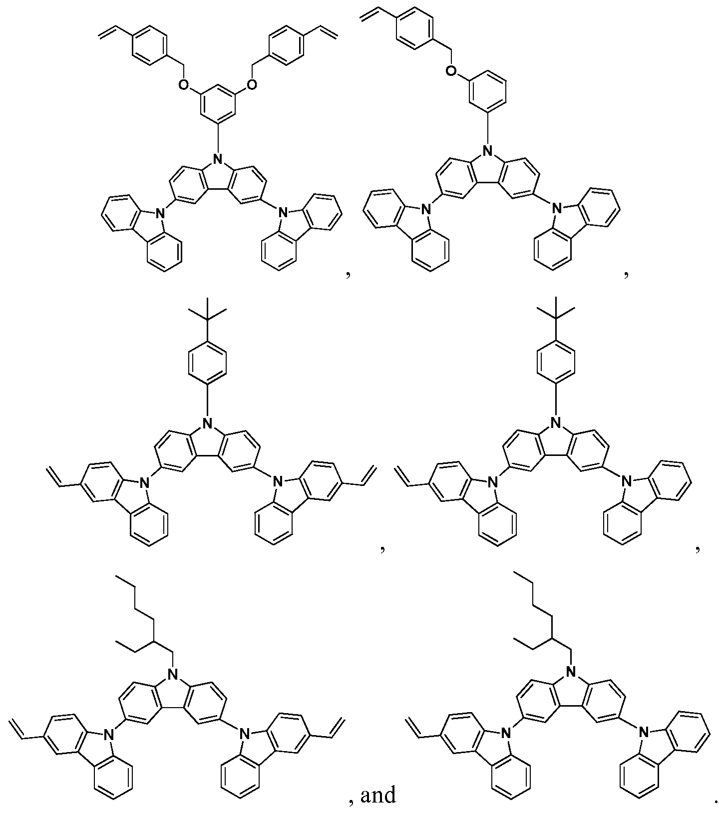
20. The composition of claim 1, wherein the one or more first compounds do not comprise a 2-phenyl-5-phenyl-l,3,4-oxadiazole group.
21. The composition of claim 1, further comprising one or more second compounds.
22. The composition of claim 1, further comprising one or more second compounds comprising one or more moieties selected from the group consisting of electron transporter, solubilizing groups, compatibilizing groups, and crosslinking groups.
23. The composition of claim 9, further comprising one or more second compounds comprising at least one crosslinking group, said crosslinking group comprises at least one reactive group RG having similar reactivity to the reactive group RG of the one or more first compounds.
24. The composition of claim 1, wherein the one or more first compounds comprise one or more moieties selected from the group consisting of electron transporter, solubilizing groups, and compatibilizing groups.
25. The composition of claim 1, wherein the one or more first compounds are represented by formula (I).
26. A composition comprising one or more first compounds represented by formula (XIII) or formula (XIV):

wherein Rl, R2, R3, R4, R5, R6, R7, R8, R9, RIO, Rl l, R12, R13, R14, R15, R16, R17, R18, R19, R20, R21, R22, and R23 are each independently selected from the group consisting of hydrogen, halogen, optionally substituted alkyl, optionally substituted aryl, optionally substituted heteroalkyl, optionally substituted heteroaryl, and crosslinking group; wherein said crosslinking group comprises a reactive group RG optionally linked to a linker group L selected from the group consisting of optionally substituted alkylene, optionally substituted arylene, optionally substituted heteroalkylene, oxyalkylene, oligo-oxyalkylene and optionally substituted heteroarylene; and
wherein at least one of the first compounds comprises at least two crosslinking groups.
27. A hole transport layer, comprising the composition of claim 1, wherein the first compound is crosslinked.
28. A hole injection layer, comprising the composition of claim 1 and a p-dopant, wherein the first compound is crosslinked.
29. The hole injection layer of claim 28, wherein the dopant is a soluble complex of Mo(VI) or Cr(VI).
30. An electroluminescence device, comprising at least an anode, a cathode, an emissive layer, and the hole transport layer of claim 27.
31. An electroluminescence device, comprising at least an anode, a cathode, an emissive layer, the hole injection layer of claims 28-29 and the hole transport layer of claim 27.
32. The electroluminescence device of claim 30, wherein the hole transport layer is solution deposited on the anode.
33. The electroluminescence device of claim 31, wherein the hole injection layer and the hole transport layer are solution deposited on the anode.
34. The electroluminescence device of claims 30-31, wherein the one or more first compounds in the hole injection layer and in the hole transport layer are thermally
crosslinked.
35. The electroluminescence device of claims 30-31, wherein the one or more first compounds in the hole injection layer and in the hole transport layer are photochemically crosslinked.
36. The electroluminescence device of claims 30-31, wherein the emissive layer comprises at least one phosphorescent emitter, and wherein the external quantum efficiency of the electroluminescence device at 1,000 cd/m is at least 5%.
37. The electroluminescence device of claims 30-31, wherein the emissive layer comprises at least one phosphorescent emitter, and wherein the external quantum efficiency of the electroluminescence device at 1,000 cd/m is at least 10%.
38. A method for making a electroluminescence device, comprising:
providing an anode layer;
depositing the hole transport layer of claim 27 from solution onto the anode layer; and
crosslinking the one or more first compounds to produce a crosslinked hole transport layer, wherein the crosslinked hole transport layer is substantially insolubilized.
39. A method for making an electroluminescence device, comprising:
providing an anode layer;
depositing the hole injection layer of claims 28-29 from solution onto the anode layer;
crosslinking the first compounds of the hole injection layer to produce a crosslinked hole injection layer, wherein the crosslinked hole injection layer is substantially insolubilized;
depositing the hole transport layer of claim 27 from solution onto the hole injection layer; and
crosslinking the first compounds of the hole transport layer to produce a crosslinked hole transport layer, wherein the crosslinked hole transport layer is substantially insolubilized.
40. The method of claims 38-39, further comprising depositing an emissive layer from solution onto the crosslinked hole transporting layer.
41. A method for making an electroluminescence device, comprising:
(i) providing a conductive substrate;
(ii) depositing a composition onto the substrate to form a layer, said composition comprising one or more first compounds represented by formula (I) or formula (II):

(II)
wherein:
Rl, R2, R3, and R4 are each independently a hydrogen, a halogen, an optionally substituted alkyl group, an optionally substituted aryl group, an optionally substituted heteroalkyl group, or an optionally substituted heteroaryl group;
XLl, XL2, XL3, and XL4 are each independently a crosslinking group; kl, k2, k3, and k4 are each 0, 1 or 2;
R is an organic group optionally comprising at least one crosslinking group; wherein at least one of the first compounds comprises at least two crosslinking groups; and
(iii) rapidly heating said layer at a temperature of 150 °C or more for 60 minutes or less, wherein the one or more first compounds are crosslinked after said heating step.
42. The method of claim 41, wherein the rapid heating step comprises heating the layer at a temperature of 200 °C or more.
43. The method of claim 41, wherein the rapid heating step comprises ramping the temperature at a rate of 100 °C/minute or more.
44. The method of claim 41, wherein the rapid heating step comprises heating the layer at a temperature of 150 °C or more for 40 minutes or less.
45. The method of claim 41, wherein the one or more first compounds are represented by formula (I).
46. A crosslinked film obtained by thermally or photochemically crosslinking a composition comprising one or more first compounds represented by formula (I) or formula (II):

(I) 
(II)
wherein:
Rl, R2, R3, and R4 are each independently a hydrogen, a halogen, an optionally substituted alkyl group, an optionally substituted aryl group, an optionally substituted heteroalkyl group, or an optionally substituted heteroaryl group;
XLl, XL2, XL3, and XL4 are each independently a crosslinking group;
kl , k2, k3, and k4 are each 0, 1 or 2;
R is an organic group optionally comprising at least one crosslinking group; and
wherein at least one of the first compounds comprises at least two crosslinking groups.
Applications Claiming Priority (2)
| Application Number | Priority Date | Filing Date | Title |
|---|---|---|---|
| US201161579418P | 2011-12-22 | 2011-12-22 | |
| US61/579,418 | 2011-12-22 |
Publications (2)
| Publication Number | Publication Date |
|---|---|
| WO2013096832A2 true WO2013096832A2 (en) | 2013-06-27 |
| WO2013096832A3 WO2013096832A3 (en) | 2013-12-27 |
Family
ID=47559721
Family Applications (1)
| Application Number | Title | Priority Date | Filing Date |
|---|---|---|---|
| PCT/US2012/071363 Ceased WO2013096832A2 (en) | 2011-12-22 | 2012-12-21 | Small molecule crosslinkable triscarbazole hole transport materials |
Country Status (1)
| Country | Link |
|---|---|
| WO (1) | WO2013096832A2 (en) |
Cited By (6)
| Publication number | Priority date | Publication date | Assignee | Title |
|---|---|---|---|---|
| KR20130105459A (en) * | 2012-03-15 | 2013-09-25 | 유니버셜 디스플레이 코포레이션 | Secondary hole transporting layer with tricarbazole compounds |
| WO2014193215A1 (en) * | 2013-05-27 | 2014-12-04 | Universiti Malaya (Um) | Organic light emitting diode and method of preparation thereof |
| WO2016105161A3 (en) * | 2014-12-26 | 2016-11-24 | 주식회사 두산 | Organic compound and organic electroluminescent element comprising same |
| WO2017068988A1 (en) * | 2015-10-21 | 2017-04-27 | Dic株式会社 | Active energy ray-curable composition and plastic lens |
| WO2017068989A1 (en) * | 2015-10-21 | 2017-04-27 | Dic株式会社 | Active energy ray-curable composition and plastic lens |
| US11629126B2 (en) | 2016-10-06 | 2023-04-18 | Merck Patent Gmbh | Materials for organic electroluminescent devices |
Family Cites Families (4)
| Publication number | Priority date | Publication date | Assignee | Title |
|---|---|---|---|---|
| JP2004018787A (en) * | 2002-06-19 | 2004-01-22 | Fuji Photo Film Co Ltd | Carbazole derivative, polymer of the same and light-emitting element containing the same |
| TWI354011B (en) * | 2003-05-16 | 2011-12-11 | Semiconductor Energy Lab | Carbazole derivative, organic semiconductor elemen |
| DE102009053382A1 (en) * | 2009-11-14 | 2011-05-19 | Merck Patent Gmbh | Materials for electronic devices |
| KR101736973B1 (en) * | 2010-01-15 | 2017-05-17 | 삼성전자주식회사 | Polymer and organic light emitting diode comprising the same |
-
2012
- 2012-12-21 WO PCT/US2012/071363 patent/WO2013096832A2/en not_active Ceased
Cited By (12)
| Publication number | Priority date | Publication date | Assignee | Title |
|---|---|---|---|---|
| KR20130105459A (en) * | 2012-03-15 | 2013-09-25 | 유니버셜 디스플레이 코포레이션 | Secondary hole transporting layer with tricarbazole compounds |
| KR102141720B1 (en) | 2012-03-15 | 2020-08-06 | 유니버셜 디스플레이 코포레이션 | Secondary hole transporting layer with tricarbazole compounds |
| WO2014193215A1 (en) * | 2013-05-27 | 2014-12-04 | Universiti Malaya (Um) | Organic light emitting diode and method of preparation thereof |
| WO2016105161A3 (en) * | 2014-12-26 | 2016-11-24 | 주식회사 두산 | Organic compound and organic electroluminescent element comprising same |
| WO2017068988A1 (en) * | 2015-10-21 | 2017-04-27 | Dic株式会社 | Active energy ray-curable composition and plastic lens |
| WO2017068989A1 (en) * | 2015-10-21 | 2017-04-27 | Dic株式会社 | Active energy ray-curable composition and plastic lens |
| JP6187847B1 (en) * | 2015-10-21 | 2017-08-30 | Dic株式会社 | Active energy ray-curable composition and plastic lens |
| JP6187846B1 (en) * | 2015-10-21 | 2017-08-30 | Dic株式会社 | Active energy ray-curable composition and plastic lens |
| KR20180073587A (en) * | 2015-10-21 | 2018-07-02 | 디아이씨 가부시끼가이샤 | Active energy ray-curable composition and plastic lens |
| TWI708809B (en) * | 2015-10-21 | 2020-11-01 | 日商迪愛生股份有限公司 | Active energy ray hardening composition and plastic lens |
| TWI722029B (en) * | 2015-10-21 | 2021-03-21 | 日商迪愛生股份有限公司 | Active energy ray hardening composition and plastic lens |
| US11629126B2 (en) | 2016-10-06 | 2023-04-18 | Merck Patent Gmbh | Materials for organic electroluminescent devices |
Also Published As
| Publication number | Publication date |
|---|---|
| WO2013096832A3 (en) | 2013-12-27 |
Similar Documents
| Publication | Publication Date | Title |
|---|---|---|
| CN104053664B (en) | Iridium complex compound and solution composition containing the compound, organic electroluminescent element, display device and lighting device | |
| CN109804009B (en) | Organic light emitting diode | |
| JP6791311B2 (en) | Polymers, compositions for organic electroluminescent devices, organic electroluminescent devices, organic EL display devices and organic EL lighting | |
| CN108003365B (en) | Organic compound film and its application in organic electronic device | |
| TWI464135B (en) | Monoamine compound, charge transport material, charge transport film composition, organic electroluminescence device, organic EL display device, and organic EL illumination | |
| CN104411743B (en) | High molecular compound, charge transporting polymer, composition for organic electroluminescence element, organic electroluminescence element, organic EL display device, and organic EL lighting | |
| CN103403045B (en) | Organic electroluminescent device polymkeric substance and employ the organic electroluminescent device of its cured article | |
| KR20170102014A (en) | COMPOUND, COMPOSITIONS CONTAINING THE SAME, | |
| CN105027677B (en) | Treatment liquid containing ionic compound, organic electronic device, and method for producing organic electronic device | |
| WO2013096832A2 (en) | Small molecule crosslinkable triscarbazole hole transport materials | |
| KR20220115778A (en) | Organic electroluminescent material and device thereof | |
| US10364316B2 (en) | Conjugated polymer containing ethynyl crosslinking group, mixture, formulation, organic electronic device containing the same and application therof | |
| Ameen et al. | Curing temperature reduction and performance improvement of solution-processable hole-transporting materials for phosphorescent OLEDs by manipulation of cross-linking functionalities and core structures | |
| Cho et al. | All solution-processed red organic light-emitting diode based on a new thermally cross-linked heteroleptic Ir (iii) complex | |
| WO2013096918A1 (en) | Crosslinking triscarbazole hole transport polymers | |
| CN106575719B (en) | Organic electronic components with cross-linked organic electronic functional layers and alkyne ethers useful for the manufacture of the components | |
| CN103443140B (en) | Curable composition, cured product, and organic electroluminescent element using same | |
| Jung et al. | Deep‐red light‐emitting phosphorescent dendrimer encapsulated tris‐[2‐benzo [b] thiophen‐2‐yl‐pyridyl] iridium (III) core for light‐emitting device applications | |
| EP3699231B1 (en) | Novel polymer and organic light-emitting device comprising the same | |
| WO2013096921A1 (en) | Non-crosslinked polystyrene triscarbazole hole transport materials | |
| CN104169336A (en) | Curable composition, cured product, and organic electroluminescent device using the same | |
| CN113906577B (en) | Organic light-emitting devices | |
| CN1995097B (en) | Blue electroluminescent polymer, method of preparing blue electroluminescent polymer, and organic electroluminescent device employing the same | |
| JP6972589B2 (en) | Organic electronics materials, and organic layers, organic electronics elements, organic electroluminescence elements, display elements, lighting devices, and display devices using the materials. | |
| TW201827563A (en) | Organic electronic material, ink composition, organic electronic component, and method of manufacturing organic electronic component |
Legal Events
| Date | Code | Title | Description |
|---|---|---|---|
| 121 | Ep: the epo has been informed by wipo that ep was designated in this application |
Ref document number: 12815953 Country of ref document: EP Kind code of ref document: A2 |
|
| 122 | Ep: pct application non-entry in european phase |
Ref document number: 12815953 Country of ref document: EP Kind code of ref document: A2 |