WO2013056473A1 - 用于液晶显示器过驱动控制的系统 - Google Patents
用于液晶显示器过驱动控制的系统 Download PDFInfo
- Publication number
- WO2013056473A1 WO2013056473A1 PCT/CN2011/081228 CN2011081228W WO2013056473A1 WO 2013056473 A1 WO2013056473 A1 WO 2013056473A1 CN 2011081228 W CN2011081228 W CN 2011081228W WO 2013056473 A1 WO2013056473 A1 WO 2013056473A1
- Authority
- WO
- WIPO (PCT)
- Prior art keywords
- image data
- overdrive
- frame image
- timing control
- current frame
- Prior art date
- Legal status (The legal status is an assumption and is not a legal conclusion. Google has not performed a legal analysis and makes no representation as to the accuracy of the status listed.)
- Ceased
Links
Images

Classifications
-
- G—PHYSICS
- G09—EDUCATION; CRYPTOGRAPHY; DISPLAY; ADVERTISING; SEALS
- G09G—ARRANGEMENTS OR CIRCUITS FOR CONTROL OF INDICATING DEVICES USING STATIC MEANS TO PRESENT VARIABLE INFORMATION
- G09G3/00—Control arrangements or circuits, of interest only in connection with visual indicators other than cathode-ray tubes
- G09G3/20—Control arrangements or circuits, of interest only in connection with visual indicators other than cathode-ray tubes for presentation of an assembly of a number of characters, e.g. a page, by composing the assembly by combination of individual elements arranged in a matrix no fixed position being assigned to or needed to be assigned to the individual characters or partial characters
- G09G3/2092—Details of a display terminals using a flat panel, the details relating to the control arrangement of the display terminal and to the interfaces thereto
-
- G—PHYSICS
- G09—EDUCATION; CRYPTOGRAPHY; DISPLAY; ADVERTISING; SEALS
- G09G—ARRANGEMENTS OR CIRCUITS FOR CONTROL OF INDICATING DEVICES USING STATIC MEANS TO PRESENT VARIABLE INFORMATION
- G09G3/00—Control arrangements or circuits, of interest only in connection with visual indicators other than cathode-ray tubes
- G09G3/20—Control arrangements or circuits, of interest only in connection with visual indicators other than cathode-ray tubes for presentation of an assembly of a number of characters, e.g. a page, by composing the assembly by combination of individual elements arranged in a matrix no fixed position being assigned to or needed to be assigned to the individual characters or partial characters
- G09G3/34—Control arrangements or circuits, of interest only in connection with visual indicators other than cathode-ray tubes for presentation of an assembly of a number of characters, e.g. a page, by composing the assembly by combination of individual elements arranged in a matrix no fixed position being assigned to or needed to be assigned to the individual characters or partial characters by control of light from an independent source
- G09G3/36—Control arrangements or circuits, of interest only in connection with visual indicators other than cathode-ray tubes for presentation of an assembly of a number of characters, e.g. a page, by composing the assembly by combination of individual elements arranged in a matrix no fixed position being assigned to or needed to be assigned to the individual characters or partial characters by control of light from an independent source using liquid crystals
- G09G3/3611—Control of matrices with row and column drivers
- G09G3/3648—Control of matrices with row and column drivers using an active matrix
-
- G—PHYSICS
- G09—EDUCATION; CRYPTOGRAPHY; DISPLAY; ADVERTISING; SEALS
- G09G—ARRANGEMENTS OR CIRCUITS FOR CONTROL OF INDICATING DEVICES USING STATIC MEANS TO PRESENT VARIABLE INFORMATION
- G09G2320/00—Control of display operating conditions
- G09G2320/02—Improving the quality of display appearance
- G09G2320/0252—Improving the response speed
-
- G—PHYSICS
- G09—EDUCATION; CRYPTOGRAPHY; DISPLAY; ADVERTISING; SEALS
- G09G—ARRANGEMENTS OR CIRCUITS FOR CONTROL OF INDICATING DEVICES USING STATIC MEANS TO PRESENT VARIABLE INFORMATION
- G09G2340/00—Aspects of display data processing
- G09G2340/16—Determination of a pixel data signal depending on the signal applied in the previous frame
Definitions
- the utility model relates to an overdrive technology, in particular to a system for overdrive control of a liquid crystal display.
- the overdrive control architecture mainly includes: an image scaling device that provides an LCD panel to display an image for scaling (Vedio) Scaler) 11.
- LVDS Low-voltage differential signal receiving device
- a first synchronous dynamic random access memory (SDRAM) 13 that stores data of a previous frame of data currently required to display an image, and an overdrive controller that controls overdrive (Over Driver) Controler, ODC) 14, stored with LUT (Lookup An electrically erasable programmable read only memory (EEROM) 15 and a timing control circuit 16; the image scaling device 11 is provided with a second synchronization dynamic for storing current frame data required for currently displaying an image Random access memory 110.
- RGB in the figure Pixel indicates that the transmission is image display data
- DE Data Enable
- the transmission is an address signal in LVDS
- DCK Data Clock
- the workflow of the overdrive control system is as follows:
- the image scaling device 11 transmits the current frame data required for displaying an image on the LCD panel to the overdrive controller 14 through the low voltage differential signal receiving device 12; the image scaling device 11 and the low voltage differential signal receiving device 12 transmit The data format of the data is LVDS format.
- the overdrive controller 14 reads out the previous frame data stored in the first synchronous dynamic random access memory 13; and stores the current frame data and the previous frame data transmitted by the low voltage differential signal receiving device 12 in the electrically erasable In the write programmable read only memory 15, the lookup table is used to compare and obtain the compensated corrected image data; the comparison can use a 7*7 matrix;
- the overdrive controller 14 transmits the compensated corrected image data to the timing control circuit 16.
- T-con (Timing The controller, the timing control circuit 16) externally needs to set a first synchronous dynamic random access memory 13 for storing the previous frame of image data, where the first synchronous dynamic random access memory 13 is connected to the overdrive controller 14; and the image zooming device 11 internally has a second synchronous dynamic random access memory 110 for storing the previous frame of image data;
- the main purpose of the utility model is to provide a system for overdrive control of a liquid crystal display, which reduces production cost and improves data processing efficiency.
- the utility model provides a system for overdrive control of a liquid crystal display, comprising a timing control board and an image scaling device, wherein the timing control board comprises an overdrive controller, a memory for storing the LUT and a timing control circuit; and the storage of the LUT
- the timing control board comprises an overdrive controller, a memory for storing the LUT and a timing control circuit; and the storage of the LUT
- the memory and timing controllers are all connected to the overdrive controller
- the image scaling device stores current frame image data and previous frame image data
- the timing control panel further includes two low voltage differentials respectively connected to the overdrive controller a signal receiving device; the two low voltage differential signal receiving devices are all connected to the image scaling device;
- the two low-voltage differential signal receiving devices respectively receive current frame image data and previous frame image data transmitted by the image scaling device and transmit to the overdrive controller; the overdrive controller will display the current frame image data After comparing the previous frame image data with the LUT, the compensated corrected current frame image data is obtained; the overdrive controller outputs the compensated corrected current frame image data to the timing control circuit.
- the two low voltage differential signal receiving devices are coupled to the image scaling device via an LVDS interface.
- the two low voltage differential signal receiving devices are each connected to the overdrive controller through a data transmission line, a synchronization signal line, and a clock signal line.
- the memory storing the LUT is an electrically erasable programmable read only memory.
- the image scaling device sets a second storage device to store current frame image data and previous frame image data.
- the second storage device is a synchronous dynamic random access memory.
- the invention provides a system for overdrive control of a liquid crystal display, comprising a timing control board and an image scaling device, the timing control board comprising an overdrive controller, a memory for storing the LUT and a timing control circuit; the memory for storing the LUT
- the timing controller is connected to the overdrive controller;
- the image scaling device is configured to set a second storage device that stores current frame image data and previous frame image data;
- the timing control panel further includes two separate and overdrive controls Connected to the low voltage differential signal receiving device, the two low voltage differential signal receiving devices are respectively connected to the overdrive controller through a data transmission line, a synchronization signal line and a clock signal line; the two low voltage differential signal receiving devices are both associated with the image scaling device connection;
- the two low-voltage differential signal receiving devices respectively receive current frame image data and previous frame image data transmitted by the image scaling device and transmit to the overdrive controller; the overdrive controller will display the current frame image data After comparing the previous frame image data with the LUT, the compensated corrected current frame image data is obtained; the overdrive controller outputs the compensated corrected current frame image data to the timing control circuit.
- the two low voltage differential signal receiving devices are coupled to the image scaling device via an LVDS interface.
- the memory storing the LUT is an electrically erasable programmable read only memory.
- the second storage device is a synchronous dynamic random access memory.
- the utility model transmits the current frame image data of the second storage device and the previous frame image data in the image scaling device to the overdrive controller for processing by the two low-voltage differential signal receiving devices, that is, the current frame image data and the previous frame image.
- the data is compared and corrected with the LUT, and the corrected current frame image data is transmitted to the timing control circuit.
- FIG. 1 is a schematic diagram of a hardware architecture of a liquid crystal display overdrive control system in the prior art
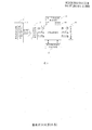
- FIG. 2 is a schematic structural view of a system for overdrive control of a liquid crystal display of the present invention.
- the system includes: a timing control board 30 and an image scaling device 31 (Vedio Scaler), the timing control board 30 includes an overdrive controller 33 (Over Driver Controler (ODC), a memory 34 storing the LUT, and a timing control circuit 35; the storage LUT (Lookup The memory 34 and the timing control circuit 35 of the table, the overdrive query table are all connected to the overdrive controller 33; the image scaling device 31 stores the current frame image data and the previous frame image data; the timing control panel 30 further includes two Low voltage differential signal receiving device 32 (LVDS) respectively connected to the overdrive controller 33 Receiver); the two low-voltage differential signal receiving devices 32 are each connected to the image scaling device 31; the two low-voltage differential signal receiving devices 32 respectively receive the current frame image data and the previous frame image data transmitted by the image scaling device 31, and Transmitting to the overdrive controller 33; the overdrive controller 33 compares the current
- LVDS Low voltage differential signal receiving device
- RGB in the figure Pixel indicates that the transmission is image display data; DE (Data Enable) indicates that the transmission is an address signal in LVDS; DCK (Data Clock) indicates that the transmission is a unit clock signal; the data format of the data transmitted between the image scaling device 31 and the low voltage differential signal receiving device 32 is in the LVDS format.
- the image data that the display panel needs to display first needs to be scaled by the image scaling device 31.
- the two low-voltage differential signal receiving devices 32 respectively receive the scaled current frame image data and the previous frame image data of the image scaling device 31, and then forwarded to the overdrive controller 33; the overdrive controller 33 receives the current frame
- the image data and the previous frame image data, and the read query table are read from the memory 34 storing the LUT, and the gray scale of the two frames of image data is compared using the overdrive lookup table to obtain the overdrive voltage and the current frame image.
- the gray scale of the data is corrected to obtain the corrected image data.
- the overdrive controller 33 then transmits the corrected current frame image data to the timing control circuit 35, and the level signal required to convert the current frame image data into an LCD panel is sent to the LCD panel for display.
- a second storage device 310 is provided in the image scaling device 31.
- the memory 34 storing the LUT may be an electrically erasable programmable read only memory (EEROM); the second storage device 310 may be a synchronous dynamic random access memory (SDRAM).
- An overdrive lookup table in which the overdrive voltage is stored in the memory 34 storing the LUT.
- the second storage device 310 stores image data that needs to be displayed in a plurality of frames, and at least includes current frame image data and previous frame image data.
- the process of the image scaling device 31 transmitting the two frames of image data to the overdrive controller 33 through the two low voltage differential signal receiving devices 32 is specifically as follows:
- the image scaling device 31 transmits the current frame image data and the previous frame image data in the second storage device 310 set thereto to the two low-voltage differential signal receiving devices 32 through the two LVDS interfaces in the same time period.
- the two low voltage differential signal receiving devices 32 are further transferred to the overdrive controller 33.
- the image scaling device 31 and the two low voltage differential signal receiving devices 32 are connected by an LVDS interface.
- the respective two low-voltage differential signal receiving devices 32 are connected to the overdrive controller 33 via data transmission lines, address signal lines, and clock signal lines, respectively.
- the data transmission line is used for transmitting image data; the synchronization signal line is used for transmitting a synchronization signal to control the opening and closing of the image data transmission; and the synchronization signal line is for transmitting a clock signal to control the time of transmission of the image data.
- the data transmission line is used to transmit image display data (RGB Pixel); the address signal line is used to transmit an address signal (DE, Data Enable) in the LVDS; the clock signal line is used to transmit a unit clock signal (DCK, Data) Clock).
- the system for overdrive control of the liquid crystal display transmits the current frame image data of the second storage device and the previous frame image data in the image scaling device 31 to the overdrive controller through the two low voltage differential signal receiving devices 32. 33 is driven, so that a single user can save the SDRAM of the previous frame image data, which reduces the product cost; at the same time, the time for reading and writing the previous frame image data in the SDRAM can be saved, and the data processing effect is improved.
Landscapes
- Engineering & Computer Science (AREA)
- Physics & Mathematics (AREA)
- Computer Hardware Design (AREA)
- General Physics & Mathematics (AREA)
- Theoretical Computer Science (AREA)
- Chemical & Material Sciences (AREA)
- Crystallography & Structural Chemistry (AREA)
- Liquid Crystal Display Device Control (AREA)
- Control Of Indicators Other Than Cathode Ray Tubes (AREA)
Abstract
一种用于液晶显示器过驱动控制的系统,包括时序控制板(30)和图像缩放装置(31)。时序控制板(30)包括过驱动控制器(33),两个分别与过驱动控制器(33)连接的低压差分信号接收装置(32),存放LUT的存储器(34)和时序控制电路(35)。所述两个低压差分信号接收装置(32)均与图像缩放装置(31)连接,并分别接收图像缩放装置(31)传送的当前帧图像数据和前一帧图像数据,然后传输至过驱动控制器(33)。过驱动控制器(33)将当前帧图像数据和前一帧图像数据数据与LUT进行比较,得到经过补偿修正的当前帧图像数据,然后传输至时序控制电路(35)。
Description
技术领域
本实用新型涉及到过驱动技术,特别涉及到一种用于液晶显示器过驱动控制的系统。
背景技术
目前大尺寸的LCD(Liquid Crystal Display,液晶显示器)面板,通常会采用过驱动(Over
Driver,OD)技术减少灰阶响应时间,以提升动画显示性能。
图1是现有技术中常用的过驱动控制系统的硬件架构示意图;参照图1,该过驱动控制架构主要包括:提供LCD面板显示图像进行缩放的图像缩放装置(Vedio
Scaler)11、传送缩放后显示图像数据的低压差分信号接收装置(LVDS
Receiver)12、存储当前显示图像所需数据的上一帧数据的第一同步动态随机存储器(SDRAM)13、控制过驱动进行的过驱动控制器(Over Driver
Controler,ODC)14、存储有LUT(Lookup
table,过驱动查询表)的电可擦写可编程只读存储器(EEROM)15以及时序控制电路16;该图像缩放装置11设置有用于存储当前显示图像所需数据的当前帧数据第二同步动态随机存储器110。图中RGB
Pixel表示传输为图像显示数据;DE(Data Enable)表示传输为LVDS中的地址信号;DCK(Data Clock)表示传输为单位时钟信号。
该过驱动控制系统的工作流程如下:
(1)该图像缩放装置11将LCD面板显示图像所需的当前帧数据通过低压差分信号接收装置12传送至过驱动控制器14中;该图像缩放装置11与低压差分信号接收装置12之间传送数据的数据格式为LVDS格式。
(2)过驱动控制器14将存于第一同步动态随机存储器13中的上一帧数据读出;再将低压差分信号接收装置12传送的当前帧数据以及上一帧数据存入电可擦写可编程只读存储器15中,使用查表的方式进行比较,得到经过补偿修正的图像数据;该比较可使用7*7矩阵;
(3)过驱动控制器14将补偿修正后的图像数据传输至时序控制电路16。
现有技术中的过驱动控制架构的缺点为:
T-con(Timing
Controller,时序控制电路16)外部需设置第一同步动态随机存储器13,用于存储上一帧图像数据,此处该第一同步动态随机存储器13连接于过驱动控制器14;而该图像缩放装置11内部本身也有第二同步动态随机存储器110存储上一帧图像数据;
T-con从第一同步动态随机存储器13中存取数据需要花费运算时间。
发明内容
本实用新型的主要目的为提供一种用于液晶显示器过驱动控制的系统,降低了生产成本,提高了数据处理效率。
本实用新型提出一种用于液晶显示器过驱动控制的系统,包括时序控制板和图像缩放装置,所述时序控制板包括过驱动控制器、存放LUT的存储器和时序控制电路;所述存放LUT的存储器、时序控制器均与过驱动控制器连接;所述图像缩放装置存储有当前帧图像数据和前一帧图像数据;所述时序控制板还包括两个分别与过驱动控制器连接的低压差分信号接收装置;该两个低压差分信号接收装置均与图像缩放装置连接;
所述两个低压差分信号接收装置分别接收图像缩放装置传送的当前帧图像数据和前一帧图像数据,并传输至所述过驱动控制器;所述过驱动控制器将所述当前帧图像数据和前一帧图像数据与LUT进行比较后,得到经过补偿修正的当前帧图像数据;过驱动控制器再将该补偿修正后的当前帧图像数据输出至时序控制电路。
优选地,所述两个低压差分信号接收装置通过LVDS接口与图像缩放装置连接。
优选地,所述两个低压差分信号接收装置各自通过数据传输线、同步信号线以及时钟信号线与过驱动控制器连接。
优选地,所述存放LUT的存储器为电可擦写可编程只读存储器。
优选地,所述图像缩放装置设置第二存储设备,存储当前帧图像数据和前一帧图像数据。
优选地,所述第二存储设备为同步动态随机存储器。
本发明提出一种用于液晶显示器过驱动控制的系统,包括时序控制板和图像缩放装置,所述时序控制板包括过驱动控制器、存放LUT的存储器和时序控制电路;所述存放LUT的存储器、时序控制器均与过驱动控制器连接;所述图像缩放装置设置第二存储设备,存储有当前帧图像数据和前一帧图像数据;所述时序控制板还包括两个分别与过驱动控制器连接的低压差分信号接收装置,所述两个低压差分信号接收装置各自通过数据传输线、同步信号线以及时钟信号线与过驱动控制器连接;该两个低压差分信号接收装置均与图像缩放装置连接;
所述两个低压差分信号接收装置分别接收图像缩放装置传送的当前帧图像数据和前一帧图像数据,并传输至所述过驱动控制器;所述过驱动控制器将所述当前帧图像数据和前一帧图像数据与LUT进行比较后,得到经过补偿修正的当前帧图像数据;过驱动控制器再将该补偿修正后的当前帧图像数据输出至时序控制电路。
优选地,所述两个低压差分信号接收装置通过LVDS接口与图像缩放装置连接。
优选地,所述存放LUT的存储器为电可擦写可编程只读存储器。
优选地,所述第二存储设备为同步动态随机存储器。
本实用新型通过两低压差分信号接收装置,将图像缩放装置中第二存储装置的当前帧图像数据以及前一帧图像数据发送至过驱动控制器进行处理,即将当前帧图像数据与前一帧图像数据同LUT进行比较修正,再将修正后的当前帧图像数据传输给时序控制电路。如此可节省一单独存储前一帧图像数据的SDRAM,降低了产品成本;同时,可节约读写该SDRAM中前一帧图像数据的时间,提高数据处理效果。
附图说明
图1 是现有技术中液晶显示器过驱动控制系统的硬件架构示意图;
图2 是本实用新型用于液晶显示器过驱动控制的系统的结构示意图。
本实用新型目的的实现、功能特点及优点将结合实施例,参照附图做进一步说明。
具体实施方式
应当理解,此处所描述的具体实施例仅仅用以解释本实用新型,并不用于限定本实用新型。
图2是本实用新型第二实施例中用于液晶显示器过驱动控制的系统的结构示意图。如图2所示,该系统包括:时序控制板30和图像缩放装置31(Vedio
Scaler),该时序控制板30包括过驱动控制器33(Over Driver
Controler,ODC)、存放LUT的存储器34和时序控制电路35;该存放LUT(Lookup
table,过驱动查询表)的存储器34、时序控制电路35均与过驱动控制器33连接;该图像缩放装置31存储有当前帧图像数据和前一帧图像数据;该时序控制板30还包括两个分别与过驱动控制器33连接的低压差分信号接收装置32(LVDS
Receiver);该两个低压差分信号接收装置32均与图像缩放装置31连接;该两低压差分信号接收装置32分别接收图像缩放装置31传送的当前帧图像数据和前一帧图像数据,并将其传输至所述过驱动控制器33;该过驱动控制器33将该当前帧图像数据和前一帧图像数据与LUT进行比较后,得到经过补偿修正的当前帧图像数据;驱动控制器再将该补偿修正后的当前帧图像数据输出至时序控制电路35。图中RGB
Pixel表示传输为图像显示数据;DE(Data Enable)表示传输为LVDS中的地址信号;DCK(Data
Clock)表示传输为单位时钟信号;该图像缩放装置31与低压差分信号接收装置32之间传送数据的数据格式为LVDS格式。
LCD(Liquid Crystal
Display,液晶显示器)面板需要显示的图像数据首先需经过该图像缩放装置31进行缩放。该两低压差分信号接收装置32分别接收该图像缩放装置31经过缩放后的当前帧图像数据以及前一帧图像数据,然后转发至过驱动控制器33中;该过驱动控制器33接收该当前帧图像数据以及前一帧图像数据,以及从存放LUT的存储器34中读取过驱动查询表,并使用该过驱动查询表比较该两帧图像数据的灰阶,获取过驱动电压,对当前帧图像数据的灰阶进行修正,得到补偿修正后的图像数据。该过驱动控制器33再是将修正后的当前帧图像数据发送至时序控制电路35中,将该当前帧图像数据转换为LCD面板所需的电平信号发送至该LCD面板进行显示。
该图像缩放装置31中设置有第二存储设备310。上述存放LUT的存储器34可为电可擦写可编程只读存储器(EEROM);上述第二存储设备310可为同步动态随机存储器(SDRAM)。该存放LUT的存储器34中存储有过驱动电压的过驱动查询表。上述第二存储设备310,存储有若干帧需要显示的图像数据,其中至少包括当前帧图像数据和前一帧图像数据。上述图像缩放装置31将两帧图像数据通过两低压差分信号接收装置32发送至过驱动控制器33的过程具体为:
该图像缩放装置31将其设置的第二存储设备310中的当前帧图像数据以及前一帧图像数据,在同一时间周期内通过两LVDS接口分别发送至两低压差分信号接收装置32。再通过该两低压差分信号接收装置32转送至过驱动控制器33。该图像缩放装置31与该两低压差分信号接收装置32之间,通过LVDS接口连接。该两低压差分信号接收装置32的各自与过驱动控制器33之间,分别通过数据传输线、地址信号线以及时钟信号线连接。该数据传输线用于传送图像数据;该同步信号线用于传送同步信号,控制该图像数据传送的开启与关闭;该同步信号线用于传送时钟信号,控制该图像数据传送的时间。该数据传输线用于传输图像显示数据(RGB
Pixel);该地址信号线用于传输LVDS中的地址信号(DE,Data Enable);该时钟信号线用于传输单位时钟信号(DCK,Data
Clock)。
本实施例中用于液晶显示器过驱动控制的系统,通过两低压差分信号接收装置32,将图像缩放装置31中第二存储装置的当前帧图像数据以及前一帧图像数据发送至过驱动控制器33进行过驱动,如此可节省一单独用户存储前一帧图像数据的SDRAM,降低了产品成本;同时,可节省掉在该SDRAM中读写前一帧图像数据的时间,提高数据处理效果。
以上所述仅为本实用新型的优选实施例,并非因此限制本实用新型的专利范围,凡是利用本实用新型说明书及附图内容所作的等效结构或等效流程变换,或直接或间接运用在其他相关的技术领域,均同理包括在本实用新型的专利保护范围内。
Claims (10)
- 一种用于液晶显示器过驱动控制的系统,包括时序控制板和图像缩放装置,所述时序控制板包括过驱动控制器、存放LUT的存储器和时序控制电路;所述存放LUT的存储器、时序控制器均与过驱动控制器连接;所述图像缩放装置存储有当前帧图像数据和前一帧图像数据;其特征在于,所述时序控制板还包括两个分别与过驱动控制器连接的低压差分信号接收装置;该两个低压差分信号接收装置均与图像缩放装置连接;所述两个低压差分信号接收装置分别接收图像缩放装置传送的当前帧图像数据和前一帧图像数据,并传输至所述过驱动控制器;所述过驱动控制器将所述当前帧图像数据和前一帧图像数据与LUT进行比较后,得到经过补偿修正的当前帧图像数据;过驱动控制器再将该补偿修正后的当前帧图像数据输出至时序控制电路。
- 根据权利要求1所述的用于液晶显示器过驱动控制的系统,其特征在于,所述两个低压差分信号接收装置通过LVDS接口与图像缩放装置连接。
- 根据权利要求1或2所述的用于液晶显示器过驱动控制的系统,其特征在于,所述两个低压差分信号接收装置各自通过数据传输线、同步信号线以及时钟信号线与过驱动控制器连接。
- 根据权利要求1或2所述的用于液晶显示器过驱动控制的系统,其特征在于,所述存放LUT的存储器为电可擦写可编程只读存储器。
- 根据权利要求1或2所述的用于液晶显示器过驱动控制的系统,其特征在于,所述图像缩放装置设置第二存储设备,存储当前帧图像数据和前一帧图像数据。
- 根据权利要求5所述的用于液晶显示器过驱动控制的系统,其特征在于,所述第二存储设备为同步动态随机存储器。
- 一种用于液晶显示器过驱动控制的系统,包括时序控制板和图像缩放装置,所述时序控制板包括过驱动控制器、存放LUT的存储器和时序控制电路;所述存放LUT的存储器、时序控制器均与过驱动控制器连接;所述图像缩放装置设置第二存储设备,存储有当前帧图像数据和前一帧图像数据;其特征在于,所述时序控制板还包括两个分别与过驱动控制器连接的低压差分信号接收装置,所述两个低压差分信号接收装置各自通过数据传输线、同步信号线以及时钟信号线与过驱动控制器连接;该两个低压差分信号接收装置均与图像缩放装置连接;所述两个低压差分信号接收装置分别接收图像缩放装置传送的当前帧图像数据和前一帧图像数据,并传输至所述过驱动控制器;所述过驱动控制器将所述当前帧图像数据和前一帧图像数据与LUT进行比较后,得到经过补偿修正的当前帧图像数据;过驱动控制器再将该补偿修正后的当前帧图像数据输出至时序控制电路。
- 根据权利要求7所述的用于液晶显示器过驱动控制的系统,其特征在于,所述两个低压差分信号接收装置通过LVDS接口与图像缩放装置连接。
- 根据权利要求7或8所述的用于液晶显示器过驱动控制的系统,其特征在于,所述存放LUT的存储器为电可擦写可编程只读存储器。
- 根据权利要求9所述的用于液晶显示器过驱动控制的系统,其特征在于,所述第二存储设备为同步动态随机存储器。
Priority Applications (1)
| Application Number | Priority Date | Filing Date | Title |
|---|---|---|---|
| US13/377,546 US20130100168A1 (en) | 2011-10-19 | 2011-10-25 | Overdrive controlling system for liquid crystal display |
Applications Claiming Priority (2)
| Application Number | Priority Date | Filing Date | Title |
|---|---|---|---|
| CN 201120399522 CN202275592U (zh) | 2011-10-19 | 2011-10-19 | 用于液晶显示器过驱动控制的系统 |
| CN201120399522.5 | 2011-10-19 |
Publications (1)
| Publication Number | Publication Date |
|---|---|
| WO2013056473A1 true WO2013056473A1 (zh) | 2013-04-25 |
Family
ID=46195937
Family Applications (1)
| Application Number | Title | Priority Date | Filing Date |
|---|---|---|---|
| PCT/CN2011/081228 Ceased WO2013056473A1 (zh) | 2011-10-19 | 2011-10-25 | 用于液晶显示器过驱动控制的系统 |
Country Status (2)
| Country | Link |
|---|---|
| CN (1) | CN202275592U (zh) |
| WO (1) | WO2013056473A1 (zh) |
Cited By (1)
| Publication number | Priority date | Publication date | Assignee | Title |
|---|---|---|---|---|
| CN111009225A (zh) * | 2019-12-26 | 2020-04-14 | 哈尔滨工业大学(深圳) | 一种显示屏过驱动装置、过驱动方法及显示装置 |
Families Citing this family (6)
| Publication number | Priority date | Publication date | Assignee | Title |
|---|---|---|---|---|
| CN102968971B (zh) * | 2012-11-08 | 2015-01-28 | 京东方科技集团股份有限公司 | 液晶显示驱动方法、时序控制装置及液晶显示设备 |
| CN103165092A (zh) * | 2013-02-25 | 2013-06-19 | 京东方科技集团股份有限公司 | 一种液晶显示的方法及装置 |
| CN105448223B (zh) * | 2015-12-30 | 2018-06-12 | 荆溪瑞 | 一种显示控制电路及显示装置 |
| CN105761695A (zh) | 2016-05-13 | 2016-07-13 | 京东方科技集团股份有限公司 | 驱动电路及其驱动方法和显示装置 |
| CN106856088A (zh) * | 2017-02-08 | 2017-06-16 | 昆山龙腾光电有限公司 | 显示装置及驱动方法 |
| CN107039003B (zh) * | 2017-06-14 | 2019-07-02 | 深圳市华星光电半导体显示技术有限公司 | 适合amoled补偿的数据驱动芯片架构和时序控制器架构 |
Citations (5)
| Publication number | Priority date | Publication date | Assignee | Title |
|---|---|---|---|---|
| KR20050123490A (ko) * | 2004-06-25 | 2005-12-29 | 엘지.필립스 엘시디 주식회사 | 액정표시장치 |
| CN1801301A (zh) * | 2005-01-05 | 2006-07-12 | 明基电通股份有限公司 | 可显示影像的电子装置 |
| CN1924989A (zh) * | 2005-08-31 | 2007-03-07 | Lg.菲利浦Lcd株式会社 | 液晶显示器件及其驱动方法 |
| TW200737096A (en) * | 2006-03-29 | 2007-10-01 | Novatek Microelectronics Corp | Method and apparatus of transmitting data signals and control signals via LVDS interfaces |
| CN101617357A (zh) * | 2006-10-18 | 2009-12-30 | 美国博通公司 | 视频处理数据的提供 |
-
2011
- 2011-10-19 CN CN 201120399522 patent/CN202275592U/zh not_active Expired - Lifetime
- 2011-10-25 WO PCT/CN2011/081228 patent/WO2013056473A1/zh not_active Ceased
Patent Citations (5)
| Publication number | Priority date | Publication date | Assignee | Title |
|---|---|---|---|---|
| KR20050123490A (ko) * | 2004-06-25 | 2005-12-29 | 엘지.필립스 엘시디 주식회사 | 액정표시장치 |
| CN1801301A (zh) * | 2005-01-05 | 2006-07-12 | 明基电通股份有限公司 | 可显示影像的电子装置 |
| CN1924989A (zh) * | 2005-08-31 | 2007-03-07 | Lg.菲利浦Lcd株式会社 | 液晶显示器件及其驱动方法 |
| TW200737096A (en) * | 2006-03-29 | 2007-10-01 | Novatek Microelectronics Corp | Method and apparatus of transmitting data signals and control signals via LVDS interfaces |
| CN101617357A (zh) * | 2006-10-18 | 2009-12-30 | 美国博通公司 | 视频处理数据的提供 |
Cited By (1)
| Publication number | Priority date | Publication date | Assignee | Title |
|---|---|---|---|---|
| CN111009225A (zh) * | 2019-12-26 | 2020-04-14 | 哈尔滨工业大学(深圳) | 一种显示屏过驱动装置、过驱动方法及显示装置 |
Also Published As
| Publication number | Publication date |
|---|---|
| CN202275592U (zh) | 2012-06-13 |
Similar Documents
| Publication | Publication Date | Title |
|---|---|---|
| WO2013056473A1 (zh) | 用于液晶显示器过驱动控制的系统 | |
| CN106157917B (zh) | 一种能够降低功耗的显示器驱动装置及其驱动方法 | |
| CN101751882B (zh) | 多面板显示设备及其驱动方法 | |
| CN101739980B (zh) | 多面板显示设备及其驱动方法 | |
| CN101673521B (zh) | 一种液晶显示装置和数字图像信号处理的方法 | |
| WO2018170984A1 (zh) | 一种显示面板的驱动方法、时序控制器及液晶显示器 | |
| CN102097050B (zh) | 一种实现显示信号无缝切换的装置和方法 | |
| CN103247249B (zh) | 显示控制电路、显示控制方法及显示装置 | |
| KR20120057369A (ko) | 액정표시장치 | |
| WO2018036050A1 (zh) | 一种时钟控制器自适应的方法及装置 | |
| WO2013033928A1 (zh) | Lcd过激驱动方法、装置及液晶显示器 | |
| WO2021203778A1 (zh) | 显示装置、显示系统 | |
| TW201222510A (en) | Liquid crystal display device and driving method thereof | |
| WO2012113166A1 (zh) | 液晶显示器及其驱动方法 | |
| WO2019227785A1 (zh) | 显示器驱动系统 | |
| WO2017020333A1 (zh) | 一种液晶显示器及其控制方法 | |
| WO2017219399A1 (zh) | 显示驱动电路及液晶显示面板 | |
| WO2018209755A1 (zh) | 显示面板及显示装置 | |
| WO2018157419A1 (zh) | 驱动电路及液晶显示装置 | |
| CN115862560B (zh) | 信号传输方法、控制器、源驱动器和电子设备 | |
| CN101281739A (zh) | 液晶显示装置及其驱动方法 | |
| TWI420485B (zh) | 液晶顯示器驅動電路及方法 | |
| KR102494149B1 (ko) | 데이터 구동 회로 및 그를 이용한 표시 장치 | |
| CN115862559B (zh) | 信号传输方法、控制器、源驱动器和电子设备 | |
| CN201965886U (zh) | 液晶屏数字信号发生器 |
Legal Events
| Date | Code | Title | Description |
|---|---|---|---|
| WWE | Wipo information: entry into national phase |
Ref document number: 13377546 Country of ref document: US |
|
| 121 | Ep: the epo has been informed by wipo that ep was designated in this application |
Ref document number: 11874143 Country of ref document: EP Kind code of ref document: A1 |
|
| NENP | Non-entry into the national phase |
Ref country code: DE |
|
| 122 | Ep: pct application non-entry in european phase |
Ref document number: 11874143 Country of ref document: EP Kind code of ref document: A1 |