WO2013054791A1 - 撮像レンズ及び撮像装置 - Google Patents
撮像レンズ及び撮像装置 Download PDFInfo
- Publication number
- WO2013054791A1 WO2013054791A1 PCT/JP2012/076133 JP2012076133W WO2013054791A1 WO 2013054791 A1 WO2013054791 A1 WO 2013054791A1 JP 2012076133 W JP2012076133 W JP 2012076133W WO 2013054791 A1 WO2013054791 A1 WO 2013054791A1
- Authority
- WO
- WIPO (PCT)
- Prior art keywords
- lens
- imaging
- image
- imaging lens
- object side
- Prior art date
- Legal status (The legal status is an assumption and is not a legal conclusion. Google has not performed a legal analysis and makes no representation as to the accuracy of the status listed.)
- Ceased
Links
Images









Classifications
-
- G—PHYSICS
- G02—OPTICS
- G02B—OPTICAL ELEMENTS, SYSTEMS OR APPARATUS
- G02B13/00—Optical objectives specially designed for the purposes specified below
- G02B13/001—Miniaturised objectives for electronic devices, e.g. portable telephones, webcams, PDAs, small digital cameras
- G02B13/0015—Miniaturised objectives for electronic devices, e.g. portable telephones, webcams, PDAs, small digital cameras characterised by the lens design
- G02B13/002—Miniaturised objectives for electronic devices, e.g. portable telephones, webcams, PDAs, small digital cameras characterised by the lens design having at least one aspherical surface
- G02B13/003—Miniaturised objectives for electronic devices, e.g. portable telephones, webcams, PDAs, small digital cameras characterised by the lens design having at least one aspherical surface having two lenses
Definitions
- the present invention relates to an imaging lens suitable for an imaging device using a solid-state imaging device such as a CCD (Charge Coupled Devices) type image sensor or a CMOS (Complementary Meta 1-Oxide Semiconductor) type image sensor.
- a solid-state imaging device such as a CCD (Charge Coupled Devices) type image sensor or a CMOS (Complementary Meta 1-Oxide Semiconductor) type image sensor.
- an imaging lens having a configuration of 3 to 5 lenses has been proposed because high performance is required.
- a sub-camera imaging lens low-pixels of VGA or less have been common so far, so a single-lens imaging lens was the main one.
- high performance capable of dealing with high pixels such as 1.3 million pixels and 2 million pixels has been demanded.
- a single-lens imaging lens has been proposed.
- imaging lenses having a two-lens configuration imaging lenses having a positive / negative configuration as in Patent Documents 1 to 4 are known.
- the imaging lens described in Patent Document 1 has a problem that the curvature of the image side surface of the second lens is strong, the sag amount to the inflection point is large, and the moldability is deteriorated.
- a lens made of a hard material such as a glass mold lens
- the moldability deteriorates, the lens surface shape variation during molding becomes large, and it becomes difficult to ensure sufficient optical performance.
- the curvature of the image side surface of the second lens is weak, so the aberration correction is insufficient.
- the curvature of the object side surface of the second lens becomes strong. There is a problem that the prospective angle within the effective diameter increases and the moldability deteriorates.
- the imaging lens described in Patent Document 3 is an imaging lens in consideration of moldability, the curvature of the image side surface of the first lens is weak and the Petzval sum is large, so correction of field curvature is insufficient.
- the total lens length is further shortened, there is a problem that performance deterioration occurs and it is difficult to cope with the increase in the number of pixels of the image sensor.
- the imaging lens described in Patent Document 4 has a problem that the moldability is poor because the curvature on the second lens object side is too strong.
- the present invention has been made in view of such problems, and uses a two-lens imaging lens in which various aberrations are corrected while having better moldability than the conventional type, and the imaging lens.
- An object is to provide an imaging device.
- the present invention aims at miniaturization at a level satisfying the following expression. By satisfying this range, the entire imaging apparatus can be reduced in size and weight.
- L Distance on the optical axis from the lens surface closest to the object side to the image-side focal point of the entire imaging lens system 2Y: diagonal length of the imaging surface of the solid-state imaging device (diagonal length of the rectangular effective pixel region of the solid-state imaging device)
- the image-side focal point refers to an image point when a parallel light beam parallel to the optical axis is incident on the imaging lens.
- a parallel plate such as an optical low-pass filter, an infrared cut filter, or a seal glass of a solid-state image sensor package is disposed between the image-side surface of the imaging lens and the image-side focal position, the parallel lens
- the flat plate portion is calculated as the above L value after the air conversion distance. More preferably, the range of the following formula is good. L / 2Y ⁇ 0.90 (7) '
- the imaging lens according to claim 1 includes an aperture stop, a first lens, and a second lens in order from the object side.
- the first lens is a positive meniscus lens having a convex surface on the object side and a concave surface on the image side
- the second lens is a negative lens having a paraxial concave surface facing the image side surface
- the image side surface is an imaging lens having an aspherical surface having an inflection point and a convex shape on the periphery, The following conditional expression is satisfied.
- n1 Refractive index of the first lens with respect to the d-line
- n2 Refractive index of the second lens with respect to the d-line
- r2 Radius of curvature of the side surface of the first lens (mm)
- r3 radius of curvature (mm) of the side surface of the second lens object
- r4 radius of curvature of the side surface of the second lens image (mm)
- the first lens is configured as a positive lens and the second lens is configured as a negative lens, a so-called telephoto type can be obtained, so that the optical total length can be shortened. Furthermore, by making the shape of the first lens a meniscus lens having a convex surface facing the object side, the principal point position of the first lens with strong power can be set on the object side, so that the optical total length can be further shortened. In general, if the optical total length is shortened, the exit pupil position gets closer to the image plane.Therefore, securing telecentricity is a problem, but by placing the aperture stop closest to the object side, the exit pupil position is moved closer to the object side.
- the incident angle of light on the peripheral portion of the screen is reduced. It can be reduced to ensure good telecentricity.
- conditional expression (1) When the value of conditional expression (1) is less than the upper limit, the concave surface on the side surface of the first lens image can be given power, so that the Petzval sum can be reduced and the curvature of field can be corrected well. In addition, when the value of conditional expression (1) exceeds the lower limit, it is possible to prevent the occurrence of higher-order aberrations due to the concave surface becoming too strong. Furthermore, the imaging lens of the present invention desirably satisfies the following conditional expression (1 ′). ⁇ 0.90 ⁇ (1-n1) f / r2 ⁇ 0.30 (1 ′)
- conditional expression (2) When the value of conditional expression (2) is lower than the upper limit or higher than the lower limit, the curvature of the object side surface of the second lens is weakened, so the expected angle of the optical surface is reduced and the moldability is improved. Furthermore, the imaging lens of the present invention desirably satisfies the following conditional expression (2 ′). ⁇ 0.15 ⁇ (n2-1) f / r3 ⁇ 0.15 (2 ′)
- conditional expression (3) When the value of conditional expression (3) is below the upper limit, the power of the image side surface of the second lens is increased, so that the Petzval sum is reduced and the curvature of field can be corrected well. Moreover, since the concave surface on the side surface of the second lens image is weakened when the value of conditional expression (3) exceeds the lower limit, the amount of sag up to the inflection point leading to the peripheral positive power can be suppressed to a small value. Can maintain good moldability. Furthermore, the imaging lens of the present invention desirably satisfies the following conditional expression (3 ′). ⁇ 0.20 ⁇ (1-n2) f / r4 ⁇ 0.05 (3 ′)
- the imaging lens described in claim 2 is characterized in that, in the invention described in claim 1, the following conditional expression is satisfied. -10.0 ⁇ (SAG3 / f) ⁇ 1000 ⁇ 0 (4) However, SAG3: Sag amount at 70% of the effective diameter of the second lens object side surface
- the optical surface can be made a gentle surface, so that the moldability can be kept good.
- the “effective diameter” refers to the position through which the outermost light beam of the light beam formed at the highest image height passes.
- the imaging lens according to claim 3 is characterized in that, in the invention according to claim 1 or 2, the imaging lens has an infrared cut coat on the object side surface of the second lens.
- IR cut function By providing the IR cut function on the optical surface, another member having an infrared cut function such as an IR cut filter can be omitted, leading to cost reduction.
- IR cut coating When IR cut coating is applied to the optical surface, it is known that there is a difference in film thickness between the central portion and the peripheral portion of the lens because the lens has a curvature.
- the surface satisfying the formulas (2) and (4) has a small surface angle, it is possible to suppress a film thickness variation that occurs when an IR cut coat is used as an optical surface. The shift of the wavelength characteristic to the short wavelength side can be minimized.
- An imaging lens according to a fourth aspect of the invention is characterized in that, in the invention according to any one of the first to third aspects, the following conditional expression is satisfied. 0.30 ⁇ d3 / f ⁇ 0.60 (5) However, d3: Axial thickness (mm) of the second lens
- the imaging lens of the present invention desirably satisfies the following conditional expression (5 ′). 0.35 ⁇ d3 / f ⁇ 0.50 (5 ')
- the imaging lens described in claim 5 is characterized in that, in the invention described in any one of claims 1 to 4, the following conditional expression is satisfied. -20.0 ⁇ f2 / f1 ⁇ -5.0 (6) However, f1: Focal length (mm) of the first lens f2: Focal length (mm) of the second lens
- Conditional expression (6) is a conditional expression representing the ratio of the power of the first lens and the second lens.
- conditional expression (6) is below the upper limit, the power of the first lens is sufficiently strong with respect to the power of the second lens, so that the total optical length can be kept small.
- conditional expression (6) exceeds the lower limit, the second lens has a certain amount of power with respect to the power of the first lens, so the Petzval sum can be reduced and the field curvature is corrected well. can do.
- the imaging lens of the present invention desirably satisfies the following conditional expression (6 ′). ⁇ 17.0 ⁇ f2 / f1 ⁇ 8.0 (6 ′)
- the image pickup lens according to claim 6 is characterized in that, in the invention according to any one of claims 1 to 5, the second lens is made of glass.
- the second lens satisfying the expressions (2) and (3) is easy to mold and has excellent moldability when the material is glass. Further, in a lens made of a hard material such as a glass mold lens, when the moldability is deteriorated, the lens surface shape variation at the time of molding becomes large, and it becomes difficult to ensure sufficient optical performance.
- the image pickup lens described in claim 7 is characterized in that, in the invention described in any one of claims 1 to 5, the second lens is made of resin.
- the second lens satisfying the expressions (2) and (3) can ensure a highly accurate surface shape even when contracted during molding.
- An imaging apparatus includes the imaging lens according to any one of the first to seventh aspects and a solid-state imaging element, and satisfies the following expression.
- L Distance on the optical axis from the lens surface closest to the object side to the image-side focal point of the entire imaging lens system 2Y: diagonal length of the imaging surface of the solid-state imaging device (diagonal length of the rectangular effective pixel region of the solid-state imaging device)
- An image pickup apparatus is characterized in that, in the invention according to the eighth aspect, the following expression is satisfied.
- an imaging lens having a two-lens configuration in which various aberrations are corrected while having better moldability than the conventional type, and an imaging apparatus using the imaging lens.
- FIGS. 2A and 2B are diagrams showing a mobile phone T, in which FIG. 1A is a view of the folded mobile phone opened and viewed from the inside, and FIG. 2B is a view of the folded mobile phone opened and viewed from the outside.
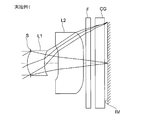
- 1 is a cross-sectional view of an imaging lens according to Example 1.
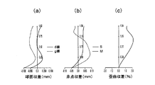
- FIG. FIG. 6 is an aberration diagram of spherical aberration (a), astigmatism (b), and distortion (c) of the imaging lens according to Example 1; 6 is a cross-sectional view of an imaging lens according to Example 2.
- FIG. 1 is a cross-sectional view of an imaging lens according to Example 1.
- FIG. 1 is a cross-sectional view of an imaging lens according to Example 1.
- FIG. 6 is an aberration
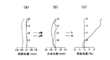
- FIG. 6 is an aberration diagram of spherical aberration (a), astigmatism (b), and distortion (c) of the imaging lens according to Example 2; 6 is a cross-sectional view of an imaging lens according to Example 3.
- FIG. FIG. 6 is an aberration diagram of spherical aberration (a), astigmatism (b), and distortion aberration (c) of the imaging lens according to Example 3; 6 is a cross-sectional view of an imaging lens according to Example 4.
- FIG. FIG. 6 is an aberration diagram of spherical aberration (a), astigmatism (b), and distortion aberration (c) of the imaging lens according to Example 4; 6 is a cross-sectional view of an imaging lens according to Example 5.
- FIG. 10 is an aberration diagram of spherical aberration (a), astigmatism (b), and distortion aberration (c) of the imaging lens according to Example 5; 6 is a cross-sectional view of an imaging lens according to Example 6.
- FIG. FIG. 10 is an aberration diagram of spherical aberration (a), astigmatism (b), and distortion (c) of the imaging lens according to Example 6; 10 is a cross-sectional view of an imaging lens according to Example 7.
- FIG. FIG. 10 is an aberration diagram of spherical aberration (a), astigmatism (b), and distortion (c) of the imaging lens according to Example 7;
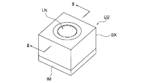
- FIG. 1 is a perspective view of an imaging apparatus LU according to the present embodiment
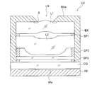
- FIG. 2 is a cross-sectional view of the configuration of FIG. 1 taken along line II-II and viewed in the direction of the arrow.
- the imaging device LU is a CMOS type image sensor IM as a solid-state imaging device having a photoelectric conversion unit IMa, and imaging that causes the photoelectric conversion unit (light receiving surface) IMa of the image sensor IM to capture a subject image.
- a lens LN and an external connection terminal (electrode) (not shown) for transmitting and receiving the electrical signal are provided, and these are integrally formed.
- the imaging lens LN is composed of a glass or resin-made first lens L1 and a glass or resin-made second lens L2 in order from the object side (upper side in FIG. 2).
- the lens can be formed by a glass mold or a droplet method.
- the first lens L1 is a positive meniscus lens having a convex surface on the object side and a concave surface on the image side.
- the second lens L2 is a negative lens having a paraxial concave surface on the image side surface, and the image side surface has an inflection point.
- the periphery includes an aspheric surface having a convex shape, and the following conditional expression is satisfied.
- n1 Refractive index of the first lens L1 with respect to the d-line
- n2 Refractive index with respect to the d-line of the second lens L2
- r2 Radius of curvature of the first lens image side surface (mm)
- r3 radius of curvature of the second lens object side surface (mm)
- r4 radius of curvature of the second lens image side surface (mm)
- f Focal length of the entire system (mm)
- a photoelectric conversion unit IMa as a light receiving unit in which pixels (photoelectric conversion elements) are two-dimensionally arranged is formed in the center of a plane on the light receiving side, and signal processing (not shown) is performed.
- a signal processing circuit includes a drive circuit unit that sequentially drives each pixel to obtain a signal charge, an A / D conversion unit that converts each signal charge into a digital signal, and a signal that forms an image signal output using the digital signal. It consists of a processing unit and the like.
- a number of pads are arranged near the outer edge of the light receiving side plane of the image sensor IM, and are connected to the image sensor IM via wires (not shown).
- the image sensor IM converts a signal charge from the photoelectric conversion unit IMa into an image signal such as a digital YUV signal and outputs the image signal to a predetermined circuit via a wire (not shown).
- Y is a luminance signal
- the solid-state imaging device is not limited to the CMOS image sensor, and other devices such as a CCD may be used.
- the image sensor IM is connected to an external circuit (for example, a control circuit included in a host device of a portable terminal mounted with an imaging device) via an external connection terminal, and a voltage or a clock for driving the image sensor IM from the external circuit. It is possible to receive a signal and to output a digital YUV signal to an external circuit.
- an external circuit for example, a control circuit included in a host device of a portable terminal mounted with an imaging device
- the upper part of the image sensor IM is sealed with a cover glass CG.
- a parallel plate-shaped IR cut filter F is provided above the cover glass CG (object side) with a spacer SP3 interposed therebetween, and a second lens is disposed above the cover glass CG at a predetermined distance with a spacer SP2 interposed therebetween.
- the flange portion of L2 (outside of the lens portion) is fixed, and further above that, the flange portion (outside of the lens portion) of the first lens L1 is fixed via a spacer SP1.
- the outer sides of these lenses L1 and L2 are covered with a housing BX, and the lower surface of the upper flange BXa of the housing BX is supported in contact with the upper surface of the flange portion (outside of the lens portion) of the first lens L1.
- the lower end of the housing BX is in contact with the cover glass CG.
- An opening formed in the upper flange BXa of the housing BX constitutes a diaphragm S.
- FIG. 3A is a view of the folded mobile phone opened from the inside
- FIG. 3B is a view of the folded mobile phone opened from the outside.
- the mobile phone T includes an upper casing 71 as a case having display screens D1 and D2 and a lower casing 72 having an operation button B via a hinge 73. It is connected.
- the main imaging device MC for photographing a landscape or the like is provided on the surface side of the upper housing 71, and the imaging device LU including the above-described wide-angle imaging lens LN is the upper housing 71. And provided on the display screen D1.
- the imaging lens LN can image the upper body of the user himself holding the mobile phone T with his / her hand, with the imaging device LU facing the imaging device LU.
- a so-called videophone can be realized by making a normal call.
- the mobile phone T is not limited to a folding type.
- the surface described with “*” after each surface number is a surface having an aspheric shape, and the shape of the aspheric surface has the vertex of the surface as the origin and the X axis in the optical axis direction.
- the height in the direction perpendicular to the optical axis is represented by the following “Equation 1”.
- a power of 10 (for example, 2.5 ⁇ 10 ⁇ 02 ) is represented by using E (for example, 2.5e ⁇ 002).
- E for example, 2.5e ⁇ 002
- the surface number of the lens data was given in order with the object side of the first lens as one surface.
- the unit of the numerical value showing the length as described in an Example shall be mm.
- Example 1 Table 1 shows lens data in Example 1. 4 is a sectional view of the lens of Example 1.
- FIG. The imaging lens according to the first exemplary embodiment includes, in order from the object side, an aperture stop S, a first lens L1, and a second lens L2 in order from the object side.
- the first lens L1 has a convex surface on the object side and a concave surface on the image side. It is a positive meniscus lens
- the second lens L2 is a negative lens having a paraxial concave surface directed to the image side surface
- the image side surface has an aspheric surface having an inflection point and a convex shape in the periphery.
- F is an infrared cut filter
- CG is a cover glass
- IM is a solid-state image sensor.
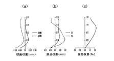
- FIG. 5 is an aberration diagram of Example 1 (spherical aberration (a), astigmatism (b), distortion (c)).
- the solid line represents the spherical aberration amount with respect to the d line and the dotted line, respectively
- the solid line represents the sagittal surface and the dotted line represents the meridional surface (hereinafter the same).
- Example 2 shows lens data in Example 2.
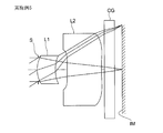
- 6 is a sectional view of the lens of Example 2.
- the imaging lens of Example 2 includes an aperture stop S, a first lens L1, and a second lens L2 in order from the object side, and from the object side.
- the first lens L1 has a convex surface on the object side and a concave surface on the image side. It is a positive meniscus lens
- the second lens L2 is a negative lens having a paraxial concave surface directed to the image side surface
- the image side surface has an aspheric surface having an inflection point and a convex shape in the periphery.
- F is an infrared cut filter
- CG is a cover glass
- IM is a solid-state image sensor.
- FIG. 7 is an aberration diagram of Example 2 (spherical aberration (a), astigmatism (b), distortion (c)).
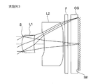
- FIG. 8 is a sectional view of the lens of Example 3.
- the imaging lens according to the third exemplary embodiment includes an aperture stop S, a first lens L1, and a second lens L2 in order from the object side.
- the first lens L1 has a convex surface on the object side and a concave surface on the image side. It is a positive meniscus lens
- the second lens L2 is a negative lens having a paraxial concave surface directed to the image side surface
- the image side surface has an aspheric surface having an inflection point and a convex shape in the periphery.
- F is an infrared cut filter
- CG is a cover glass
- IM is a solid-state image sensor.
- FIG. 9 is an aberration diagram of Example 3 (spherical aberration (a), astigmatism (b), distortion (c)).
- FIG. 10 is a sectional view of the lens of Example 4.
- the imaging lens according to the fourth exemplary embodiment includes an aperture stop S, a first lens L1, and a second lens L2 in order from the object side, and has a convex surface on the object side and a concave surface on the image side. It is a positive meniscus lens, and the second lens L2 is a negative lens having a paraxial concave surface directed to the image side surface, and the image side surface has an aspheric surface having an inflection point and a convex shape in the periphery.
- F is an infrared cut filter
- CG is a cover glass
- IM is a solid-state image sensor.
- FIG. 11 is an aberration diagram of Example 4 (spherical aberration (a), astigmatism (b), distortion (c)).
- Example 5 shows lens data in Example 5.
- 12 is a sectional view of the lens of Example 5.
- the imaging lens according to the fifth exemplary embodiment includes an aperture stop S, a first lens L1, and a second lens L2 in order from the object side, and has a convex surface on the object side and a concave surface on the image side. It is a positive meniscus lens, and the second lens L2 is a negative lens having a paraxial concave surface directed to the image side surface, and the image side surface has an aspheric surface having an inflection point and a convex shape in the periphery.
- CG is a cover glass and IM is a solid-state image sensor.
- an IR cut coat is applied to the object side surface of the second lens L2.
- FIG. 13 is an aberration diagram of Example 5 (spherical aberration (a), astigmatism (b), distortion (c)).
- Example 6 shows lens data in Example 6.
- FIG. 14 is a sectional view of the lens of Example 6.
- the imaging lens of Example 6 includes an aperture stop S, a first lens L1, and a second lens L2 in order from the object side, and the first lens L1 has a convex surface on the object side and a concave surface on the image side. It is a positive meniscus lens, and the second lens L2 is a negative lens having a paraxial concave surface directed to the image side surface, and the image side surface has an aspheric surface having an inflection point and a convex shape in the periphery.
- F is an infrared cut filter
- CG is a cover glass
- IM is a solid-state image sensor.
- FIG. 15 is an aberration diagram of Example 6 (spherical aberration (a), astigmatism (b), distortion (c)).
- Example 7 shows lens data in Example 7.
- FIG. 16 is a sectional view of the lens of Example 7.
- the imaging lens of Example 7 includes an aperture stop S, a first lens L1, and a second lens L2 in order from the object side, in order from the object side, and the first lens L1 has a convex surface on the object side and a concave surface on the image side. It is a positive meniscus lens, and the second lens L2 is a negative lens having a paraxial concave surface directed to the image side surface, and the image side surface has an aspheric surface having an inflection point and a convex shape in the periphery.
- F is an infrared cut filter
- CG is a cover glass
- IM is a solid-state image sensor.
- FIG. 17 is an aberration diagram of Example 7 (spherical aberration (a), astigmatism (b), distortion (c)).
- Table 8 summarizes the values of the examples corresponding to each conditional expression.
Landscapes
- Physics & Mathematics (AREA)
- General Physics & Mathematics (AREA)
- Optics & Photonics (AREA)
- Lenses (AREA)
Abstract
成形性などが良好でありながら、諸収差が補正された2枚構成の撮像レンズおよび、この撮像レンズを用いた撮像装置を提供する。撮像レンズは、物体側から順に開口絞り、第1レンズ、第2レンズからなり、前記第1レンズは、物体側に凸面、像側に凹面を有する正メニスカスレンズであり、前記第2レンズは、像側面に近軸凹面を向けた負レンズで、前記像側面は変曲点を持ち周辺が凸形状を有する非球面を備えてなる撮像レンズであって、以下の条件式を満足する。 -1.10<(1-n1)f/r2<-0.20 (1) -0.18<(n2-1)f/r3< 0.18 (2) -0.25<(1-n2)f/r4<-0.02 (3) 但し、n1:前記第1レンズのd線に対する屈折率 n2:前記第2レンズのd線に対する屈折率 r2:前記第1レンズ像側面の曲率半径(mm) r3:前記第2レンズ物体側面の曲率半径(mm) r4:前記第2レンズ像側面の曲率半径(mm)
Description
本発明は、CCD(Charge Coupled Devices)型イメージセンサやCMOS(Complementary Meta1-Oxide Semiconductor)型イメージセンサ等の固体撮像素子を用いた撮像装置に好適な撮像レンズに関するものである。
近年、CCD型イメージセンサあるいはCMOS型イメージセンサ等の固体撮像素子を用いた撮像素子の高性能化、小型化に伴い、撮像装置を備えた携帯電話(スマートフォンを含む)や携帯情報端末が普及しつつある。また、これらの撮像装置に搭載される撮像レンズには、さらなる小型化、高性能化への要求が高まっている。近頃ではこのような携帯端末に高画素・高性能のメインカメラと、低画素・小型のサブカメラの2つが搭載されている場合も多い。
メインカメラ用途の撮像レンズとしては、高性能化が必要とされるため3枚乃至5枚構成の撮像レンズが提案されている。一方で、サブカメラ用途の撮像レンズとしては、これまではVGA以下の低画素が一般的であったため、1枚構成の撮像レンズが主であったが、近頃ではサブカメラの高画素化が進み、低背(短全長)に加え、130万画素、200万画素などの高画素へ対応できる高性能化も求められるようになってきており、そのため1枚構成に比べ高性能化が可能な2枚構成の撮像レンズが提案されている。
2枚構成の撮像レンズとしては、特許文献1~4のような、正負構成の撮像レンズが知られている。
しかしながら、特許文献1に記載の撮像レンズでは、第2レンズの像側面の曲率が強く、変曲点までのサグ量が大きく、成形性が悪くなってしまうという問題がある。特にガラスモールドレンズのような硬い材料のレンズにおいては、成形性が悪くなると成形の際のレンズ面形状バラつきが大きくなってしまい、十分な光学性能の確保が困難となる。
また、特許文献2に記載の撮像レンズでは、第2レンズの像側面の曲率が弱いため収差補正が不足であり、その収差補正不足を補うために、第2レンズの物体側面の曲率が強くなっており、有効径内の見込み角が大きくなり成形性が悪くなってしまうという問題がある。
また、特許文献3に記載の撮像レンズでは、成形性を考慮した撮像レンズとなっているものの、第1レンズの像側面の曲率が弱く、ペッツバール和が大きいため像面湾曲の補正が不十分であり、さらにレンズ全長を短縮した場合、性能劣化が起こり撮像素子の高画素化に対応が困難となる問題がある。
また、特許文献4に記載の撮像レンズでは、第2レンズ物体側の曲率が強過ぎるため成形性が悪いという問題がある。
本発明は、このような問題点に鑑みてなされたものであり、従来タイプより成形性などが良好でありながら、諸収差が補正された2枚構成の撮像レンズおよび、この撮像レンズを用いた撮像装置を提供することを目的とする。
ここで、小型の撮像レンズの尺度であるが、本発明では下式を満たすレベルの小型化を目指している。この範囲を満たすことで、撮像装置全体の小型軽量化が可能となる。
L/2Y<1.00 (7)
ただし、
L:撮像レンズ全系の最も物体側のレンズ面から像側焦点までの光軸上の距離
2Y:固体撮像素子の撮像面対角線長(固体撮像素子の矩形実効画素領域の対角線長)
L/2Y<1.00 (7)
ただし、
L:撮像レンズ全系の最も物体側のレンズ面から像側焦点までの光軸上の距離
2Y:固体撮像素子の撮像面対角線長(固体撮像素子の矩形実効画素領域の対角線長)
ここで、像側焦点とは撮像レンズに光軸と平行な平行光線が入射した場合の像点をいう。なお、撮像レンズの最も像側の面と像側焦点位置との間に、光学的ローパスフィルタ、赤外線カットフィルタ、または固体撮像素子パッケージのシールガラス等の平行平板が配置される場合には、平行平板部分は空気換算距離としたうえで上記Lの値を計算するものとする。また、より望ましくは下式の範囲が良い。
L/2Y<0.90 (7)’
L/2Y<0.90 (7)’
請求項1に記載の撮像レンズは、物体側から順に開口絞り、第1レンズ、第2レンズからなり、
前記第1レンズは、物体側に凸面、像側に凹面を有する正メニスカスレンズであり、
前記第2レンズは、像側面に近軸凹面を向けた負レンズで、前記像側面は変曲点を持ち周辺が凸形状を有する非球面を備えてなる撮像レンズであって、
以下の条件式を満足することを特徴とする。
-1.10<(1-n1)f/r2<-0.20 (1)
-0.18<(n2-1)f/r3< 0.18 (2)
-0.25<(1-n2)f/r4<-0.02 (3)
但し、
n1:前記第1レンズのd線に対する屈折率
n2:前記第2レンズのd線に対する屈折率
r2:前記第1レンズ像側面の曲率半径(mm)
r3:前記第2レンズ物体側面の曲率半径(mm)
r4:前記第2レンズ像側面の曲率半径(mm)
前記第1レンズは、物体側に凸面、像側に凹面を有する正メニスカスレンズであり、
前記第2レンズは、像側面に近軸凹面を向けた負レンズで、前記像側面は変曲点を持ち周辺が凸形状を有する非球面を備えてなる撮像レンズであって、
以下の条件式を満足することを特徴とする。
-1.10<(1-n1)f/r2<-0.20 (1)
-0.18<(n2-1)f/r3< 0.18 (2)
-0.25<(1-n2)f/r4<-0.02 (3)
但し、
n1:前記第1レンズのd線に対する屈折率
n2:前記第2レンズのd線に対する屈折率
r2:前記第1レンズ像側面の曲率半径(mm)
r3:前記第2レンズ物体側面の曲率半径(mm)
r4:前記第2レンズ像側面の曲率半径(mm)
第1レンズを正レンズとし、第2レンズを負レンズの構成とすることで、所謂テレフォトタイプとなるため、光学全長を短縮することが可能となる。さらに第1レンズの形状を物体側に凸面を向けたメニスカスレンズとすることで、パワーの強い第1レンズの主点位置を物体側にできるため、さらなる光学全長の短縮が可能となる。また、一般に光学全長を短縮すると射出瞳位置が像面に近付いてくるため、テレセントリック性の確保が課題となるが、開口絞りを最も物体側に置くことで射出瞳位置を物体側へ寄せ、さらに第2レンズの像側面を、変曲点を持ち周辺が凸形状を有するような非球面とする(すなわち周辺部が正のパワーを持つようにする)ことで画面周辺部への光線入射角を小さくし、良好なテレセントリック性を確保することができる。
条件式(1)の値が上限を下回ることで、第1レンズ像側面の凹面にパワーを持たせることができるため、ペッツバール和を小さくし、像面湾曲を良好に補正することが出来る。また、条件式(1)の値が下限を上回ることで、凹面が強くなり過ぎることによる高次収差の発生を防ぐことができる。さらに、本発明の撮像レンズは、望ましくは以下の条件式(1’)を満足する。
-0.90<(1-n1)f/r2<-0.30 (1’)
-0.90<(1-n1)f/r2<-0.30 (1’)
条件式(2)の値が上限を下回るか下限を上回ることで、第2レンズの物体側面の曲率が弱くなるため、光学面の見込み角が小さくなり、成形性が良好となる。さらに、本発明の撮像レンズは、望ましくは以下の条件式(2’)を満足する。
-0.15<(n2-1)f/r3< 0.15 (2’)
-0.15<(n2-1)f/r3< 0.15 (2’)
条件式(3)の値が上限を下回ることで、第2レンズの像側面のパワーが強くなるため、ペッツバール和が小さくなり、像面湾曲を良好に補正することができる。また、条件式(3)の値が下限を上回ることで、第2レンズ像側面の凹面が弱くなるため、周辺の正のパワーに至る変曲点までのサグ量を小さく抑えることができ、良好な成形性を保つことが出来る。さらに、本発明の撮像レンズは、望ましくは以下の条件式(3’)を満足する。
-0.20<(1-n2)f/r4<-0.05 (3’)
-0.20<(1-n2)f/r4<-0.05 (3’)
請求項2に記載の撮像レンズは、請求項1に記載の発明において、以下の条件式を満足することを特徴とする。
-10.0<(SAG3/f)×1000<0 (4)
ただし、
SAG3:前記第2レンズ物体側面の有効径の7割の位置におけるサグ量
-10.0<(SAG3/f)×1000<0 (4)
ただし、
SAG3:前記第2レンズ物体側面の有効径の7割の位置におけるサグ量
(4)式を満たすように、第2レンズ物体側面のサグ量を小さく抑えることで、光学面を緩やかな面とすることができるため成形性を良好に保つことができる。ここで、「有効径」とは、最も高い像高に結像する光線の最外光線が通る位置をいう。
請求項3に記載の撮像レンズは、請求項1又は2に記載の発明において、第2レンズの物体側面に赤外カットコートを有することを特徴とする。
IRカット機能を光学面に持たせることで、IRカットフィルタのような赤外カット機能を持った別部材を省略することができるため、コストダウンにつながる。光学面にIRカットコートを施す場合、レンズに曲率が付いているため、レンズ中心部と周辺部で膜厚に差が出ることが知られている。特に、(2)式、(4)式を満たしている面は面角度が小さく抑えられているため、IRカットコートを光学面にする際に発生する膜厚変動を小さく抑えることができ、コート波長特性の短波長側へのシフトを最小限に抑えることが出来る。
請求項4に記載の撮像レンズは、請求項1~3のいずれかに記載の発明において、以下の条件式を満足することを特徴とする。
0.30 < d3/f < 0.60 (5)
ただし、
d3:前記第2レンズの軸上厚(mm)
0.30 < d3/f < 0.60 (5)
ただし、
d3:前記第2レンズの軸上厚(mm)
条件式(5)の値が上限を下回ることで、第2レンズの厚さが厚くなり過ぎず、光学全長を短縮することができる。また条件式(5)の値が下限を上回ることで、第2レンズの厚さが薄くなり過ぎず、像側面の周辺部が物体側へサグを持っていても、コバ厚を確保することができるため、成形性を良好に保つことができる。さらに、本発明の撮像レンズは、望ましくは以下の条件式(5’)を満足する。
0.35 < d3/f < 0.50 (5’)
0.35 < d3/f < 0.50 (5’)
請求項5に記載の撮像レンズは、請求項1~4のいずれかに記載の発明において、以下の条件式を満足することを特徴とする。
-20.0 < f2/f1 < -5.0 (6)
ただし、
f1:前記第1レンズの焦点距離(mm)
f2:前記第2レンズの焦点距離(mm)
-20.0 < f2/f1 < -5.0 (6)
ただし、
f1:前記第1レンズの焦点距離(mm)
f2:前記第2レンズの焦点距離(mm)
条件式(6)は第1レンズと第2レンズのパワーの比を表わす条件式である。条件式(6)の値が上限を下回ることで、第2レンズのパワーに対して第1レンズのパワーが十分強くなるため、光学全長を小さく抑えることができる。また条件式(6)の値が下限を上回ることで、第1レンズのパワーに対して、第2レンズがある程度パワーを持つため、ペッツバール和を小さくすることが出来、像面湾曲を良好に補正することができる。また、全系の主点を物体側に寄せることができるため、さらなる光学全長の短縮も可能となる。
さらに、本発明の撮像レンズは、望ましくは以下の条件式(6’)を満足する。
-17.0 < f2/f1 < -8.0 (6’)
さらに、本発明の撮像レンズは、望ましくは以下の条件式(6’)を満足する。
-17.0 < f2/f1 < -8.0 (6’)
請求項6に記載の撮像レンズは、請求項1~5のいずれかに記載の発明において、前記第2レンズはガラス製であることを特徴とする。(2)、(3)式を満たす第2レンズは、金型の加工が容易で、素材をガラスとした場合の成形性に優れる。更にガラスモールドレンズのような硬い材料のレンズにおいては、成形性が悪くなると成形の際のレンズ面形状バラつきが大きくなってしまい、十分な光学性能の確保が困難となる。
請求項7に記載の撮像レンズは、請求項1~5のいずれかに記載の発明において、前記第2レンズは樹脂製であることを特徴とする。(2)、(3)式を満たす第2レンズは、成形時に収縮しても高精度な面形状を確保できる。
請求項8に記載の撮像装置は、請求項1~7のいずれかに記載の撮像レンズと、固体撮像素子とを有し、以下の式を満たすことを特徴とする。
L/2Y<1.00 (7)
ただし、
L:前記撮像レンズ全系の最も物体側のレンズ面から像側焦点までの光軸上の距離
2Y:前記固体撮像素子の撮像面対角線長(前記固体撮像素子の矩形実効画素領域の対角線長)
L/2Y<1.00 (7)
ただし、
L:前記撮像レンズ全系の最も物体側のレンズ面から像側焦点までの光軸上の距離
2Y:前記固体撮像素子の撮像面対角線長(前記固体撮像素子の矩形実効画素領域の対角線長)
請求項9に記載の撮像装置は、請求項8に記載の発明において、以下の式を満たすことを特徴とする。
L/2Y<0.90 (7’)
L/2Y<0.90 (7’)
本発明によれば、従来タイプより成形性などが良好でありながら、諸収差が補正された2枚構成の撮像レンズおよび、この撮像レンズを用いた撮像装置を提供することができる。
以下、本発明の実施の形態を図面に基づいて説明する。図1は、本実施の形態にかかる撮像装置LUの斜視図であり、図2は、図1の構成を矢印II-II線で切断して矢印方向に見た断面図である。図2に示すように、撮像装置LUは、光電変換部IMaを有する固体撮像素子としてのCMOS型イメージセンサIMと、このイメージセンサIMの光電変換部(受光面)IMaに被写体像を撮像させる撮像レンズLNと、その電気信号の送受を行う不図示の外部接続用端子(電極)とを備え、これらが一体的に形成されている。
撮像レンズLNは、物体側(図2で上方)から順に、ガラス又は樹脂製の第1レンズL1と、ガラス又は樹脂製の第2レンズL2とからなる。レンズをガラスで作製する場合、ガラスモールドや液滴法で成形できる。第1レンズL1は、物体側に凸面、像側に凹面を有する正メニスカスレンズであり、第2レンズL2は、像側面に近軸凹面を向けた負レンズで、像側面は変曲点を持ち周辺が凸形状を有する非球面を備えてなり、以下の条件式を満足する。
-1.10<(1-n1)f/r2<-0.20 (1)
-0.18<(n2-1)f/r3< 0.18 (2)
-0.25<(1-n2)f/r4<-0.05 (3)
但し、
n1:第1レンズL1のd線に対する屈折率
n2:第2レンズL2のd線に対する屈折率
r2:第1レンズ像側面の曲率半径(mm)
r3:第2レンズ物体側面の曲率半径(mm)
r4:第2レンズ像側面の曲率半径(mm)
f:全系の焦点距離(mm)
-1.10<(1-n1)f/r2<-0.20 (1)
-0.18<(n2-1)f/r3< 0.18 (2)
-0.25<(1-n2)f/r4<-0.05 (3)
但し、
n1:第1レンズL1のd線に対する屈折率
n2:第2レンズL2のd線に対する屈折率
r2:第1レンズ像側面の曲率半径(mm)
r3:第2レンズ物体側面の曲率半径(mm)
r4:第2レンズ像側面の曲率半径(mm)
f:全系の焦点距離(mm)
上記イメージセンサIMは、その受光側の平面の中央部に、画素(光電変換素子)が2次元的に配置された、受光部としての光電変換部IMaが形成されており、不図示の信号処理回路に接続されている。かかる信号処理回路は、各画素を順次駆動し信号電荷を得る駆動回路部と、各信号電荷をデジタル信号に変換するA/D変換部と、このデジタル信号を用いて画像信号出力を形成する信号処理部等から構成されている。また、イメージセンサIMの受光側の平面の外縁近傍には、多数のパッド(図示略)が配置されており、不図示のワイヤを介してイメージセンサIMに接続されている。イメージセンサIMは、光電変換部IMaからの信号電荷をデジタルYUV信号等の画像信号等に変換し、ワイヤ(不図示)を介して所定の回路に出力する。ここで、Yは輝度信号、U(=R-Y)は赤と輝度信号との色差信号、V(=B-Y)は青と輝度信号との色差信号である。なお、固体撮像素子は上記CMOS型のイメージセンサに限定されるものではなく、CCD等の他のものを使用しても良い。
イメージセンサIMは、外部接続用端子を介して外部回路(例えば、撮像装置を実装した携帯端末の上位装置が有する制御回路)と接続し、外部回路からイメージセンサIMを駆動するための電圧やクロック信号の供給を受けたり、また、デジタルYUV信号を外部回路へ出力したりすることを可能とする。
イメージセンサIMの上部は、カバーガラスCGにより封止されている。カバーガラスCGの上方(物体側)には、スペーサSP3を介在させて、平行平板状のIRカットフィルタFが設けられ、その上方には、スペーサSP2を介在させて、所定の距離で第2レンズL2のフランジ部(レンズ部の外側)が固定され、更にその上方には、スペーサSP1を介在させて、第1レンズL1のフランジ部(レンズ部の外側)が固定されている。
これらレンズL1、L2の外側は、筐体BXにより覆われており、筐体BXの上部フランジBXaの下面が、第1レンズL1のフランジ部(レンズ部の外側)の上面に当接して支持されており、筐体BXの下端はカバーガラスCGに接触している。筐体BXの上部フランジBXaに形成された開口が絞りSを構成している。
次に、撮像装置を備えた携帯端末の一例として携帯電話機を図3の外観図に基づいて説明する。なお、図3(a)は折り畳んだ携帯電話機を開いて内側から見た図であり、図3(b)は折り畳んだ携帯電話機を開いて外側から見た図である。
図3(a)、(b)において、携帯電話機Tは、表示画面D1,D2を備えたケースとしての上筐体71と、操作ボタンBを備えた下筐体72とがヒンジ73を介して連結されている。本実施の形態においては、風景等を撮影するためのメインの撮像装置MCが、上筐体71の表面側に設けられ、上述した広角の撮像レンズLNを備える撮像装置LUが、上筐体71の裏面側であって表示画面D1の上に設けられている。
撮像レンズLNは、図3(a)に示すように撮像装置LUに正対した状態で、携帯電話機Tを手で把持した使用者自身の上半身を撮像装置LUにより撮像できる。その画像信号を通信している相手方の携帯電話機に送信して、こちらのユーザーの画像を表示できると共に、通常の通話を行うことにより、いわゆるテレビ電話を実現できる。なお、携帯電話機Tは折り畳み式に限定されるものではない。
(実施例)
次に、上述した実施の形態に好適な実施例について説明する。但し、以下に示す実施例により本発明が限定されるものではない。実施例における各符号の意味は以下の通りである。
FL:撮像レンズ全系の焦点距離(mm)
BF:バックフォーカス(mm)(但し、平行平板を空気換算長とした時の、平行平板を除いた最終光学面から近軸像面までの距離)
Fno :Fナンバー
w :半画角(゜)
Ymax:固体撮像素子の撮像面対角線長の半分の長さ(mm)
TL:撮像レンズ全系の最も物体側のレンズ面から像側焦点までの光軸上の距離(mm)(但し、「像側焦点」とは、撮像レンズに光軸と平行な平行光線が入射した場合の像点をいい、このときの像点は平行平板を空気換算長として求める。)
r :屈折面の曲率半径(mm)
d :軸上面間隔(mm)
nd:レンズ材料のd線の常温での屈折率
vd:レンズ材料のアッベ数
STO:開口絞り
次に、上述した実施の形態に好適な実施例について説明する。但し、以下に示す実施例により本発明が限定されるものではない。実施例における各符号の意味は以下の通りである。
FL:撮像レンズ全系の焦点距離(mm)
BF:バックフォーカス(mm)(但し、平行平板を空気換算長とした時の、平行平板を除いた最終光学面から近軸像面までの距離)
Fno :Fナンバー
w :半画角(゜)
Ymax:固体撮像素子の撮像面対角線長の半分の長さ(mm)
TL:撮像レンズ全系の最も物体側のレンズ面から像側焦点までの光軸上の距離(mm)(但し、「像側焦点」とは、撮像レンズに光軸と平行な平行光線が入射した場合の像点をいい、このときの像点は平行平板を空気換算長として求める。)
r :屈折面の曲率半径(mm)
d :軸上面間隔(mm)
nd:レンズ材料のd線の常温での屈折率
vd:レンズ材料のアッベ数
STO:開口絞り
各実施例において、各面番号の後に「*」が記載されている面が非球面形状を有する面であり、非球面の形状は、面の頂点を原点とし、光軸方向にX軸をとり、光軸と垂直方向の高さをhとして以下の「数1」で表す。

Ai:i次の非球面係数
R :基準曲率半径
K :円錐定数
である。
また、以降(表のレンズデータを含む)において、10のべき乗数(例えば、2.5×10-02)をE(例えば2.5e-002)を用いて表すものとする。また、レンズデータの面番号は第1レンズの物体側を1面として順に付与した。なお、実施例に記載の長さを表す数値の単位はすべてmmとする。
(実施例1)
実施例1におけるレンズデータを表1に示す。図4は実施例1のレンズの断面図である。実施例1の撮像レンズは、物体側から順に、物体側から順に開口絞りS、第1レンズL1、第2レンズL2からなり、第1レンズL1は、物体側に凸面、像側に凹面を有する正メニスカスレンズであり、第2レンズL2は、像側面に近軸凹面を向けた負レンズで、前記像側面は変曲点を持ち周辺が凸形状を有する非球面を備えてなる。尚、Fは赤外線カットフィルタ、CGはカバーガラス、IMは固体撮像素子である。
実施例1におけるレンズデータを表1に示す。図4は実施例1のレンズの断面図である。実施例1の撮像レンズは、物体側から順に、物体側から順に開口絞りS、第1レンズL1、第2レンズL2からなり、第1レンズL1は、物体側に凸面、像側に凹面を有する正メニスカスレンズであり、第2レンズL2は、像側面に近軸凹面を向けた負レンズで、前記像側面は変曲点を持ち周辺が凸形状を有する非球面を備えてなる。尚、Fは赤外線カットフィルタ、CGはカバーガラス、IMは固体撮像素子である。
[表1]
Reference Wave Length = 587.56 nm
unit: mm
NUM. r d nd vd eff.diameter
OBJ INFINITY 350.0000
1 INFINITY 0.0500 0.840
STO INFINITY -0.0850 0.840
3* 0.8376 0.6530 1.58313 59.44 0.904
4* 1.5995 0.4070 0.943
5* 1e+018 0.9620 1.58313 59.44 1.248
6* 12.5380 0.1000 2.334
7 INFINITY 0.1750 1.52310 54.49 3.400
8 INFINITY 0.1690 3.400
9 INFINITY 0.4000 1.52550 62.19 3.400
IMG INFINITY 0.0563
非球面係数
3:K=-4.42830e+000,A3=1.95700e-002,A4=9.65840e-001,A6=-8.98080e-001,A8=-2.17300e+001,A10=3.89000e+002,A12=-2.98010e+003,A14=1.12680e+004,A16=-1.69290e+004
4:K=-5.00000e+001,A3=4.60780e-001,A4=-4.30670e-001,A6=9.84810e+000,A8=-1.02650e+002,A10=8.50080e+002,A12=-4.59480e+003,A14=1.43470e+004,A16=-1.87400e+004
5:K=0.00000e+000,A4=-4.74040e-001,A6=1.18080e+000,A8=-1.32070e+001,A10=5.38720e+001,A12=-9.71240e+001,A14=1.83010e+002,A16=-1.01490e+003,A18=2.50480e+003,A20=-1.91630e+003
6:K=0.00000e+000,A4=-9.02160e-002,A6=-1.31520e-001,A8=2.57910e-001,A10=-3.88240e-001,A12=2.37370e-001,A14=6.04190e-002,A16=-1.63310e-001,A18=7.72210e-002,A20=-1.18490e-002
FL 2.3599
Fno 2.8224
w 64.3227
Ymax 1.5400
BF 0.694
TL 2.715
Elem Surfs Focal Length Diameter
1 3-11 2.359893 3.3685
Elem Surfs Focal Length Diameter
1 3- 4 2.291940 0.9600
2 5- 6 -21.501209 2.4360
Reference Wave Length = 587.56 nm
unit: mm
NUM. r d nd vd eff.diameter
OBJ INFINITY 350.0000
1 INFINITY 0.0500 0.840
STO INFINITY -0.0850 0.840
3* 0.8376 0.6530 1.58313 59.44 0.904
4* 1.5995 0.4070 0.943
5* 1e+018 0.9620 1.58313 59.44 1.248
6* 12.5380 0.1000 2.334
7 INFINITY 0.1750 1.52310 54.49 3.400
8 INFINITY 0.1690 3.400
9 INFINITY 0.4000 1.52550 62.19 3.400
IMG INFINITY 0.0563
非球面係数
3:K=-4.42830e+000,A3=1.95700e-002,A4=9.65840e-001,A6=-8.98080e-001,A8=-2.17300e+001,A10=3.89000e+002,A12=-2.98010e+003,A14=1.12680e+004,A16=-1.69290e+004
4:K=-5.00000e+001,A3=4.60780e-001,A4=-4.30670e-001,A6=9.84810e+000,A8=-1.02650e+002,A10=8.50080e+002,A12=-4.59480e+003,A14=1.43470e+004,A16=-1.87400e+004
5:K=0.00000e+000,A4=-4.74040e-001,A6=1.18080e+000,A8=-1.32070e+001,A10=5.38720e+001,A12=-9.71240e+001,A14=1.83010e+002,A16=-1.01490e+003,A18=2.50480e+003,A20=-1.91630e+003
6:K=0.00000e+000,A4=-9.02160e-002,A6=-1.31520e-001,A8=2.57910e-001,A10=-3.88240e-001,A12=2.37370e-001,A14=6.04190e-002,A16=-1.63310e-001,A18=7.72210e-002,A20=-1.18490e-002
FL 2.3599
Fno 2.8224
w 64.3227
Ymax 1.5400
BF 0.694
TL 2.715
Elem Surfs Focal Length Diameter
1 3-11 2.359893 3.3685
Elem Surfs Focal Length Diameter
1 3- 4 2.291940 0.9600
2 5- 6 -21.501209 2.4360
図5は実施例1の収差図(球面収差(a)、非点収差(b)、歪曲収差(c))である。ここで、球面収差図において、実線はd線、点線はg線に対する球面収差量をそれぞれ表し、非点収差図において、実線はサジタル面、点線はメリディオナル面を表す(以下、同じ)。
(実施例2)
実施例2におけるレンズデータを表2に示す。図6は実施例2のレンズの断面図である。実施例2の撮像レンズは、物体側から順に、物体側から順に開口絞りS、第1レンズL1、第2レンズL2からなり、第1レンズL1は、物体側に凸面、像側に凹面を有する正メニスカスレンズであり、第2レンズL2は、像側面に近軸凹面を向けた負レンズで、前記像側面は変曲点を持ち周辺が凸形状を有する非球面を備えてなる。尚、Fは赤外線カットフィルタ、CGはカバーガラス、IMは固体撮像素子である。
実施例2におけるレンズデータを表2に示す。図6は実施例2のレンズの断面図である。実施例2の撮像レンズは、物体側から順に、物体側から順に開口絞りS、第1レンズL1、第2レンズL2からなり、第1レンズL1は、物体側に凸面、像側に凹面を有する正メニスカスレンズであり、第2レンズL2は、像側面に近軸凹面を向けた負レンズで、前記像側面は変曲点を持ち周辺が凸形状を有する非球面を備えてなる。尚、Fは赤外線カットフィルタ、CGはカバーガラス、IMは固体撮像素子である。
[表2]
Reference Wave Length = 587.56 nm
unit: mm
NUM. r d nd vd eff.diameter
OBJ INFINITY 350.0000
1 INFINITY 0.0500 0.840
STO INFINITY -0.0682 0.840
3* 0.9004 0.6899 1.58313 59.44 0.911
4* 1.7114 0.4692 0.981
5* 8.0460 0.9004 1.58313 59.44 1.344
6* 5.7540 0.1000 2.331
7 INFINITY 0.1750 1.52310 54.49 3.400
8 INFINITY 0.1690 3.400
9 INFINITY 0.4000 1.52550 62.19 3.400
IMG INFINITY 0.0924
非球面係数
3:K=-4.40583e+000,A3=-3.52063e-003,A4=8.87648e-001,A6=-1.37562e+000,A8=-2.11593e+001,A10=4.25059e+002,A12=-3.19571e+003,A14=1.12751e+004,A16=-1.53899e+004
4:K=-5.00000e+001,A3=3.97337e-001,A4=-4.98522e-001,A6=1.03872e+001,A8=-1.15793e+002,A10=9.34071e+002,A12=-4.60672e+003,A14=1.23904e+004,A16=-1.36840e+004
5:K=0.00000e+000,A4=-5.09306e-001,A6=1.86433e+000,A8=-1.36358e+001,A10=4.81356e+001,A12=-1.00943e+002,A14=2.40224e+002,A16=-7.55447e+002,A18=1.34373e+003,A20=-8.85488e+002
6:K=0.00000e+000,A4=-1.12968e-001,A6=-1.26251e-001,A8=2.82773e-001,A10=-3.93303e-001,A12=2.24028e-001,A14=5.85290e-002,A16=-1.58629e-001,A18=8.29624e-002,A20=-1.52528e-002
FL 2.4197
Fno 2.8224
w 62.9875
Ymax 1.5400
BF 0.730
TL 2.789
Elem Surfs Focal Length Diameter
1 3-11 2.419650 3.3201
Elem Surfs Focal Length Diameter
1 3- 4 2.480770 1.0038
2 5- 6 -40.501402 2.4472
Reference Wave Length = 587.56 nm
unit: mm
NUM. r d nd vd eff.diameter
OBJ INFINITY 350.0000
1 INFINITY 0.0500 0.840
STO INFINITY -0.0682 0.840
3* 0.9004 0.6899 1.58313 59.44 0.911
4* 1.7114 0.4692 0.981
5* 8.0460 0.9004 1.58313 59.44 1.344
6* 5.7540 0.1000 2.331
7 INFINITY 0.1750 1.52310 54.49 3.400
8 INFINITY 0.1690 3.400
9 INFINITY 0.4000 1.52550 62.19 3.400
IMG INFINITY 0.0924
非球面係数
3:K=-4.40583e+000,A3=-3.52063e-003,A4=8.87648e-001,A6=-1.37562e+000,A8=-2.11593e+001,A10=4.25059e+002,A12=-3.19571e+003,A14=1.12751e+004,A16=-1.53899e+004
4:K=-5.00000e+001,A3=3.97337e-001,A4=-4.98522e-001,A6=1.03872e+001,A8=-1.15793e+002,A10=9.34071e+002,A12=-4.60672e+003,A14=1.23904e+004,A16=-1.36840e+004
5:K=0.00000e+000,A4=-5.09306e-001,A6=1.86433e+000,A8=-1.36358e+001,A10=4.81356e+001,A12=-1.00943e+002,A14=2.40224e+002,A16=-7.55447e+002,A18=1.34373e+003,A20=-8.85488e+002
6:K=0.00000e+000,A4=-1.12968e-001,A6=-1.26251e-001,A8=2.82773e-001,A10=-3.93303e-001,A12=2.24028e-001,A14=5.85290e-002,A16=-1.58629e-001,A18=8.29624e-002,A20=-1.52528e-002
FL 2.4197
Fno 2.8224
w 62.9875
Ymax 1.5400
BF 0.730
TL 2.789
Elem Surfs Focal Length Diameter
1 3-11 2.419650 3.3201
Elem Surfs Focal Length Diameter
1 3- 4 2.480770 1.0038
2 5- 6 -40.501402 2.4472
図7は実施例2の収差図(球面収差(a)、非点収差(b)、歪曲収差(c))である。
(実施例3)
実施例3におけるレンズデータを表3に示す。図8は実施例3のレンズの断面図である。実施例3の撮像レンズは、物体側から順に、物体側から順に開口絞りS、第1レンズL1、第2レンズL2からなり、第1レンズL1は、物体側に凸面、像側に凹面を有する正メニスカスレンズであり、第2レンズL2は、像側面に近軸凹面を向けた負レンズで、前記像側面は変曲点を持ち周辺が凸形状を有する非球面を備えてなる。尚、Fは赤外線カットフィルタ、CGはカバーガラス、IMは固体撮像素子である。
実施例3におけるレンズデータを表3に示す。図8は実施例3のレンズの断面図である。実施例3の撮像レンズは、物体側から順に、物体側から順に開口絞りS、第1レンズL1、第2レンズL2からなり、第1レンズL1は、物体側に凸面、像側に凹面を有する正メニスカスレンズであり、第2レンズL2は、像側面に近軸凹面を向けた負レンズで、前記像側面は変曲点を持ち周辺が凸形状を有する非球面を備えてなる。尚、Fは赤外線カットフィルタ、CGはカバーガラス、IMは固体撮像素子である。
[表3]
Reference Wave Length = 587.56 nm
unit: mm
NUM. r d nd vd eff.diameter
OBJ INFINITY 1000.0000
1 INFINITY 0.0500 0.840
STO INFINITY -0.0623 0.840
3* 0.9126 0.6779 1.48700 70.19 0.914
4* 3.8590 0.5897 1.016
5* -21.4067 1.0663 1.83400 37.19 1.340
6* 8.6587 0.1000 2.447
7 INFINITY 0.1750 1.52310 54.49 3.400
8 INFINITY 0.1690 3.400
9 INFINITY 0.4000 1.52550 62.19 3.400
IMG INFINITY 0.0541
非球面係数
3:K=-6.01260e+000,A3=3.75767e-002,A4=9.55063e-001,A6=-1.88262e+000,A8=-2.24516e+001,A10=4.54566e+002,A12=-3.18006e+003,A14=9.91073e+003,A16=-1.11738e+004
4:K=1.26415e+001,A3=4.22193e-001,A4=-1.62799e+000,A6=1.29438e+001,A8=-1.15022e+002,A10=9.16295e+002,A12=-4.67268e+003,A14=1.25006e+004,A16=-1.30901e+004
5:K=0.00000e+000,A4=-2.82274e-001,A6=9.87052e-001,A8=-1.21176e+001,A10=5.00541e+001,A12=-1.02408e+002,A14=2.13102e+002,A16=-8.12319e+002,A18=1.77837e+003,A20=-1.38317e+003
6:K=0.00000e+000,A4=-5.42322e-002,A6=-1.62605e-001,A8=3.10050e-001,A10=-3.83069e-001,A12=2.15983e-001,A14=5.90651e-002,A16=-1.58014e-001,A18=8.26739e-002,A20=-1.46841e-002
FL 2.5371
Fno 2.8224
w 60.9171
Ymax 1.5400
BF 0.694
TL 3.028
Elem Surfs Focal Length Diameter
1 3-11 2.537109 3.3215
Elem Surfs Focal Length Diameter
1 3- 4 2.282481 1.0321
2 5- 6 -7.274781 2.5797
Reference Wave Length = 587.56 nm
unit: mm
NUM. r d nd vd eff.diameter
OBJ INFINITY 1000.0000
1 INFINITY 0.0500 0.840
STO INFINITY -0.0623 0.840
3* 0.9126 0.6779 1.48700 70.19 0.914
4* 3.8590 0.5897 1.016
5* -21.4067 1.0663 1.83400 37.19 1.340
6* 8.6587 0.1000 2.447
7 INFINITY 0.1750 1.52310 54.49 3.400
8 INFINITY 0.1690 3.400
9 INFINITY 0.4000 1.52550 62.19 3.400
IMG INFINITY 0.0541
非球面係数
3:K=-6.01260e+000,A3=3.75767e-002,A4=9.55063e-001,A6=-1.88262e+000,A8=-2.24516e+001,A10=4.54566e+002,A12=-3.18006e+003,A14=9.91073e+003,A16=-1.11738e+004
4:K=1.26415e+001,A3=4.22193e-001,A4=-1.62799e+000,A6=1.29438e+001,A8=-1.15022e+002,A10=9.16295e+002,A12=-4.67268e+003,A14=1.25006e+004,A16=-1.30901e+004
5:K=0.00000e+000,A4=-2.82274e-001,A6=9.87052e-001,A8=-1.21176e+001,A10=5.00541e+001,A12=-1.02408e+002,A14=2.13102e+002,A16=-8.12319e+002,A18=1.77837e+003,A20=-1.38317e+003
6:K=0.00000e+000,A4=-5.42322e-002,A6=-1.62605e-001,A8=3.10050e-001,A10=-3.83069e-001,A12=2.15983e-001,A14=5.90651e-002,A16=-1.58014e-001,A18=8.26739e-002,A20=-1.46841e-002
FL 2.5371
Fno 2.8224
w 60.9171
Ymax 1.5400
BF 0.694
TL 3.028
Elem Surfs Focal Length Diameter
1 3-11 2.537109 3.3215
Elem Surfs Focal Length Diameter
1 3- 4 2.282481 1.0321
2 5- 6 -7.274781 2.5797
図9は実施例3の収差図(球面収差(a)、非点収差(b)、歪曲収差(c))である。
(実施例4)
実施例4におけるレンズデータを表4に示す。図10は実施例4のレンズの断面図である。実施例4の撮像レンズは、物体側から順に、物体側から順に開口絞りS、第1レンズL1、第2レンズL2からなり、第1レンズL1は、物体側に凸面、像側に凹面を有する正メニスカスレンズであり、第2レンズL2は、像側面に近軸凹面を向けた負レンズで、前記像側面は変曲点を持ち周辺が凸形状を有する非球面を備えてなる。尚、Fは赤外線カットフィルタ、CGはカバーガラス、IMは固体撮像素子である。
実施例4におけるレンズデータを表4に示す。図10は実施例4のレンズの断面図である。実施例4の撮像レンズは、物体側から順に、物体側から順に開口絞りS、第1レンズL1、第2レンズL2からなり、第1レンズL1は、物体側に凸面、像側に凹面を有する正メニスカスレンズであり、第2レンズL2は、像側面に近軸凹面を向けた負レンズで、前記像側面は変曲点を持ち周辺が凸形状を有する非球面を備えてなる。尚、Fは赤外線カットフィルタ、CGはカバーガラス、IMは固体撮像素子である。
[表4]
Reference Wave Length = 587.56 nm
unit: mm
NUM. r d nd vd eff.diameter
OBJ INFINITY 1000.0000
1 INFINITY 0.0500 0.898
STO INFINITY -0.1200 0.898
3* 0.8183 0.6304 1.58313 59.39 0.932
4* 1.4096 0.5085 0.926
5* -44.2023 0.9173 1.58313 59.39 1.299
6* 9.6803 0.1000 2.308
7 INFINITY 0.1750 1.52310 54.49 3.400
8 INFINITY 0.1690 3.400
9 INFINITY 0.3500 1.47140 65.19 3.400
IMG INFINITY 0.1085
非球面係数
3:K=-3.15541e+000,A3=-3.56669e-002,A4=9.24268e-001,A6=-1.05369e-001,A8=-3.30585e+001,A10=4.60558e+002,A12=-3.00381e+003,A14=9.82347e+003,A16=-1.28446e+004
4:K=6.90028e+000,A3=2.93943e-001,A4=-1.57193e+000,A6=1.67272e+001,A8=-1.44248e+002,A10=8.94175e+002,A12=-4.18454e+003,A14=1.34391e+004,A16=-2.09593e+004
5:K=0.00000e+000,A4=-5.35224e-001,A6=1.53473e+000,A8=-1.18000e+001,A10=4.37271e+001,A12=-1.05196e+002,A14=3.34103e+002,A16=-1.20857e+003,A18=2.26001e+003,A20=-1.52940e+003
6:K=0.00000e+000,A4=-1.27106e-001,A6=-1.02122e-001,A8=2.51530e-001,A10=-3.87909e-001,A12=2.31039e-001,A14=6.36030e-002,A16=-1.65851e-001,A18=8.24530e-002,A20=-1.40219e-002
FL 2.5407
Fno 2.8224
w 60.8935
Ymax 1.5400
BF 0.720
TL 2.776
Elem Surfs Focal Length Diameter
1 3-11 2.540692 4.3097
Elem Surfs Focal Length Diameter
1 3- 4 2.401863 0.9700
2 5- 6 -13.533350 2.5958
Reference Wave Length = 587.56 nm
unit: mm
NUM. r d nd vd eff.diameter
OBJ INFINITY 1000.0000
1 INFINITY 0.0500 0.898
STO INFINITY -0.1200 0.898
3* 0.8183 0.6304 1.58313 59.39 0.932
4* 1.4096 0.5085 0.926
5* -44.2023 0.9173 1.58313 59.39 1.299
6* 9.6803 0.1000 2.308
7 INFINITY 0.1750 1.52310 54.49 3.400
8 INFINITY 0.1690 3.400
9 INFINITY 0.3500 1.47140 65.19 3.400
IMG INFINITY 0.1085
非球面係数
3:K=-3.15541e+000,A3=-3.56669e-002,A4=9.24268e-001,A6=-1.05369e-001,A8=-3.30585e+001,A10=4.60558e+002,A12=-3.00381e+003,A14=9.82347e+003,A16=-1.28446e+004
4:K=6.90028e+000,A3=2.93943e-001,A4=-1.57193e+000,A6=1.67272e+001,A8=-1.44248e+002,A10=8.94175e+002,A12=-4.18454e+003,A14=1.34391e+004,A16=-2.09593e+004
5:K=0.00000e+000,A4=-5.35224e-001,A6=1.53473e+000,A8=-1.18000e+001,A10=4.37271e+001,A12=-1.05196e+002,A14=3.34103e+002,A16=-1.20857e+003,A18=2.26001e+003,A20=-1.52940e+003
6:K=0.00000e+000,A4=-1.27106e-001,A6=-1.02122e-001,A8=2.51530e-001,A10=-3.87909e-001,A12=2.31039e-001,A14=6.36030e-002,A16=-1.65851e-001,A18=8.24530e-002,A20=-1.40219e-002
FL 2.5407
Fno 2.8224
w 60.8935
Ymax 1.5400
BF 0.720
TL 2.776
Elem Surfs Focal Length Diameter
1 3-11 2.540692 4.3097
Elem Surfs Focal Length Diameter
1 3- 4 2.401863 0.9700
2 5- 6 -13.533350 2.5958
図11は実施例4の収差図(球面収差(a)、非点収差(b)、歪曲収差(c))である。
(実施例5)
実施例5におけるレンズデータを表5に示す。図12は実施例5のレンズの断面図である。実施例5の撮像レンズは、物体側から順に、物体側から順に開口絞りS、第1レンズL1、第2レンズL2からなり、第1レンズL1は、物体側に凸面、像側に凹面を有する正メニスカスレンズであり、第2レンズL2は、像側面に近軸凹面を向けた負レンズで、前記像側面は変曲点を持ち周辺が凸形状を有する非球面を備えてなる。尚、CGはカバーガラス、IMは固体撮像素子である。本実施例では、第2レンズL2の物体側面にIRカットコートを施している。
実施例5におけるレンズデータを表5に示す。図12は実施例5のレンズの断面図である。実施例5の撮像レンズは、物体側から順に、物体側から順に開口絞りS、第1レンズL1、第2レンズL2からなり、第1レンズL1は、物体側に凸面、像側に凹面を有する正メニスカスレンズであり、第2レンズL2は、像側面に近軸凹面を向けた負レンズで、前記像側面は変曲点を持ち周辺が凸形状を有する非球面を備えてなる。尚、CGはカバーガラス、IMは固体撮像素子である。本実施例では、第2レンズL2の物体側面にIRカットコートを施している。
[表5]
Reference Wave Length = 587.56 nm
unit: mm
NUM. r d nd vd eff.diameter
OBJ INFINITY 1000.0000
1 INFINITY 0.0500 0.820
STO INFINITY -0.0227 0.820
3* 0.9797 0.6220 1.72900 52.69 0.959
4* 1.6103 0.3949 0.958
5* 9.1068 1.1790 1.58313 59.39 1.244
6* 7.5041 0.1000 2.507
7 INFINITY 0.3500 1.47140 65.19 3.400
IMG INFINITY 0.2631
非球面係数
3:K=-8.16625e+000,A3=3.18129e-002,A4=9.89771e-001,A6=-5.88553e-001,A8=-3.76841e+001,A10=4.99253e+002,A12=-3.04725e+003,A14=9.22448e+003,A16=-1.10219e+004
4:K=4.33221e+000,A3=3.63077e-001,A4=-1.67171e+000,A6=1.58862e+001,A8=-1.35829e+002,A10=9.18381e+002,A12=-4.32723e+003,A14=1.19693e+004,A16=-1.38134e+004
5:K=0.00000e+000,A4=-4.49680e-001,A6=9.33256e-001,A8=-7.59496e+000,A10=3.81113e+001,A12=-1.56340e+002,A14=4.54470e+002,A16=-7.88247e+002,A18=5.54498e+002,A20=-2.58002e+001
6:K=0.00000e+000,A4=-8.15697e-002,A6=-7.84948e-002,A8=2.35133e-001,A10=-3.93798e-001,A12=2.37718e-001,A14=7.46519e-002,A16=-1.71513e-001,A18=8.12837e-002,A20=-1.30862e-002
FL 2.3215
Fno 2.8224
w 65.4864
Ymax 1.5400
BF 0.592
TL 2.788
Elem Surfs Focal Length Diameter
1 3- 9 2.321550 3.3701
Elem Surfs Focal Length Diameter
1 3- 4 2.423962 0.9833
2 5- 6 -100.308185 2.6834
Reference Wave Length = 587.56 nm
unit: mm
NUM. r d nd vd eff.diameter
OBJ INFINITY 1000.0000
1 INFINITY 0.0500 0.820
STO INFINITY -0.0227 0.820
3* 0.9797 0.6220 1.72900 52.69 0.959
4* 1.6103 0.3949 0.958
5* 9.1068 1.1790 1.58313 59.39 1.244
6* 7.5041 0.1000 2.507
7 INFINITY 0.3500 1.47140 65.19 3.400
IMG INFINITY 0.2631
非球面係数
3:K=-8.16625e+000,A3=3.18129e-002,A4=9.89771e-001,A6=-5.88553e-001,A8=-3.76841e+001,A10=4.99253e+002,A12=-3.04725e+003,A14=9.22448e+003,A16=-1.10219e+004
4:K=4.33221e+000,A3=3.63077e-001,A4=-1.67171e+000,A6=1.58862e+001,A8=-1.35829e+002,A10=9.18381e+002,A12=-4.32723e+003,A14=1.19693e+004,A16=-1.38134e+004
5:K=0.00000e+000,A4=-4.49680e-001,A6=9.33256e-001,A8=-7.59496e+000,A10=3.81113e+001,A12=-1.56340e+002,A14=4.54470e+002,A16=-7.88247e+002,A18=5.54498e+002,A20=-2.58002e+001
6:K=0.00000e+000,A4=-8.15697e-002,A6=-7.84948e-002,A8=2.35133e-001,A10=-3.93798e-001,A12=2.37718e-001,A14=7.46519e-002,A16=-1.71513e-001,A18=8.12837e-002,A20=-1.30862e-002
FL 2.3215
Fno 2.8224
w 65.4864
Ymax 1.5400
BF 0.592
TL 2.788
Elem Surfs Focal Length Diameter
1 3- 9 2.321550 3.3701
Elem Surfs Focal Length Diameter
1 3- 4 2.423962 0.9833
2 5- 6 -100.308185 2.6834
図13は実施例5の収差図(球面収差(a)、非点収差(b)、歪曲収差(c))である。
(実施例6)
実施例6におけるレンズデータを表6に示す。図14は実施例6のレンズの断面図である。実施例6の撮像レンズは、物体側から順に、物体側から順に開口絞りS、第1レンズL1、第2レンズL2からなり、第1レンズL1は、物体側に凸面、像側に凹面を有する正メニスカスレンズであり、第2レンズL2は、像側面に近軸凹面を向けた負レンズで、前記像側面は変曲点を持ち周辺が凸形状を有する非球面を備えてなる。尚、Fは赤外線カットフィルタ、CGはカバーガラス、IMは固体撮像素子である。
実施例6におけるレンズデータを表6に示す。図14は実施例6のレンズの断面図である。実施例6の撮像レンズは、物体側から順に、物体側から順に開口絞りS、第1レンズL1、第2レンズL2からなり、第1レンズL1は、物体側に凸面、像側に凹面を有する正メニスカスレンズであり、第2レンズL2は、像側面に近軸凹面を向けた負レンズで、前記像側面は変曲点を持ち周辺が凸形状を有する非球面を備えてなる。尚、Fは赤外線カットフィルタ、CGはカバーガラス、IMは固体撮像素子である。
[表6]
Reference Wave Length = 587.56 nm
unit: mm
NUM. r d nd vd eff.diameter
OBJ INFINITY 1000.0000
STO INFINITY 0.0500 0.814
2 INFINITY -0.1122 0.808
3* 0.7666 0.5583 1.58313 59.44 0.817
4* 1.4482 0.4740 0.854
5* -8.0747 0.8525 1.58313 59.44 1.190
6* 22.8580 0.0560 2.264
7 INFINITY 0.1450 1.52550 54.99 3.000
8 INFINITY 0.0500 3.100
9 INFINITY 0.5000 1.47140 65.19 3.200
IMG INFINITY 0.1174
非球面係数
3:K=-2.47242e+000,A3=-2.03904e-002,A4=5.28641e-001,A5=2.54642e+000,A6=-8.21916e+000,A8=3.04775e+001,A10=-4.41460e+001,A12=-2.28918e+002,A14=8.29246e+002,A16=-3.23533e+002
4:K=-3.43564e-001,A3=1.96346e-002,A4=2.34363e-001,A5=1.90841e+000,A6=-6.24281e+000,A8=4.77867e+001,A10=-1.42714e+002,A12=-1.22119e+003,A14=1.24465e+004,A16=-2.93322e+004
5:K=0.00000e+000,A3=1.63283e-001,A4=-7.76179e-001,A6=-3.60913e-001,A8=6.84326e+000,A10=-4.15614e+001,A12=8.54161e+001,A14=-1.47110e+001,A16=-1.74300e+002
6:K=0.00000e+000,A4=7.94924e-002,A6=-7.06609e-001,A8=9.79988e-001,A10=-3.12305e-001,A12=-6.37242e-001,A14=5.03041e-001,A16=1.24628e-001,A18=-2.27376e-001,A20=5.74678e-002
FL 2.3694
Fno 2.8200
w 64.2796
Ymax 1.5420
BF 0.645
TL 2.530
Elem Surfs Focal Length Diameter
1 3-11 2.369447 3.5000
Elem Surfs Focal Length Diameter
1 3- 4 2.145640 0.8537
2 5- 6 -10.129665 2.4000
Reference Wave Length = 587.56 nm
unit: mm
NUM. r d nd vd eff.diameter
OBJ INFINITY 1000.0000
STO INFINITY 0.0500 0.814
2 INFINITY -0.1122 0.808
3* 0.7666 0.5583 1.58313 59.44 0.817
4* 1.4482 0.4740 0.854
5* -8.0747 0.8525 1.58313 59.44 1.190
6* 22.8580 0.0560 2.264
7 INFINITY 0.1450 1.52550 54.99 3.000
8 INFINITY 0.0500 3.100
9 INFINITY 0.5000 1.47140 65.19 3.200
IMG INFINITY 0.1174
非球面係数
3:K=-2.47242e+000,A3=-2.03904e-002,A4=5.28641e-001,A5=2.54642e+000,A6=-8.21916e+000,A8=3.04775e+001,A10=-4.41460e+001,A12=-2.28918e+002,A14=8.29246e+002,A16=-3.23533e+002
4:K=-3.43564e-001,A3=1.96346e-002,A4=2.34363e-001,A5=1.90841e+000,A6=-6.24281e+000,A8=4.77867e+001,A10=-1.42714e+002,A12=-1.22119e+003,A14=1.24465e+004,A16=-2.93322e+004
5:K=0.00000e+000,A3=1.63283e-001,A4=-7.76179e-001,A6=-3.60913e-001,A8=6.84326e+000,A10=-4.15614e+001,A12=8.54161e+001,A14=-1.47110e+001,A16=-1.74300e+002
6:K=0.00000e+000,A4=7.94924e-002,A6=-7.06609e-001,A8=9.79988e-001,A10=-3.12305e-001,A12=-6.37242e-001,A14=5.03041e-001,A16=1.24628e-001,A18=-2.27376e-001,A20=5.74678e-002
FL 2.3694
Fno 2.8200
w 64.2796
Ymax 1.5420
BF 0.645
TL 2.530
Elem Surfs Focal Length Diameter
1 3-11 2.369447 3.5000
Elem Surfs Focal Length Diameter
1 3- 4 2.145640 0.8537
2 5- 6 -10.129665 2.4000
図15は実施例6の収差図(球面収差(a)、非点収差(b)、歪曲収差(c))である。
(実施例7)
実施例7におけるレンズデータを表7に示す。図16は実施例7のレンズの断面図である。実施例7の撮像レンズは、物体側から順に、物体側から順に開口絞りS、第1レンズL1、第2レンズL2からなり、第1レンズL1は、物体側に凸面、像側に凹面を有する正メニスカスレンズであり、第2レンズL2は、像側面に近軸凹面を向けた負レンズで、前記像側面は変曲点を持ち周辺が凸形状を有する非球面を備えてなる。尚、Fは赤外線カットフィルタ、CGはカバーガラス、IMは固体撮像素子である。
実施例7におけるレンズデータを表7に示す。図16は実施例7のレンズの断面図である。実施例7の撮像レンズは、物体側から順に、物体側から順に開口絞りS、第1レンズL1、第2レンズL2からなり、第1レンズL1は、物体側に凸面、像側に凹面を有する正メニスカスレンズであり、第2レンズL2は、像側面に近軸凹面を向けた負レンズで、前記像側面は変曲点を持ち周辺が凸形状を有する非球面を備えてなる。尚、Fは赤外線カットフィルタ、CGはカバーガラス、IMは固体撮像素子である。
[表7]
Reference Wave Length = 587.56 nm
unit: mm
NUM. r d nd vd eff.diameter
OBJ INFINITY 1000.0000
1 INFINITY 0.0500 0.831
STO INFINITY -0.0537 0.831
3* 1.0204 0.6343 1.58313 59.39 0.924
4* 2.7741 0.5599 1.038
5* 9.6828 0.9844 1.71200 31.09 1.385
6* 6.9382 0.1000 2.554
7 INFINITY 0.1750 1.52310 54.49 3.400
8 INFINITY 0.1690 3.400
9 INFINITY 0.4000 1.52550 62.19 3.400
IMG INFINITY 0.0844
非球面係数
3:K=-7.95071e+000,A3=2.35363e-002,A4=9.82407e-001,A6=-2.35928e+000,A8=-2.33433e+001,A10=4.65419e+002,A12=-3.19416e+003,A14=1.01163e+004,A16=-1.22571e+004
4:K=1.10170e+001,A3=3.78654e-001,A4=-1.54800e+000,A6=1.26252e+001,A8=-1.18094e+002,A10=9.22635e+002,A12=-4.63530e+003,A14=1.24582e+004,A16=-1.34381e+004
5:K=0.00000e+000,A4=-2.59479e-001,A6=8.63308e-001,A8=-1.18218e+001,A10=5.00452e+001,A12=-1.03338e+002,A14=2.11221e+002,A16=-7.81989e+002,A18=1.72624e+003,A20=-1.38433e+003
6:K=0.00000e+000,A4=-3.32183e-002,A6=-1.98003e-001,A8=3.20956e-001,A10=-3.80584e-001,A12=2.13360e-001,A14=5.92626e-002,A16=-1.57226e-001,A18=8.27200e-002,A20=-1.50977e-002
FL 2.3803
Fno 2.8224
w 63.6944
Ymax 1.5400
BF 0.723
TL 2.902
Elem Surfs Focal Length Diameter
1 3-11 2.380264 3.3332
Elem Surfs Focal Length Diameter
1 3- 4 2.442743 1.0382
2 5- 6 -40.404709 2.5543
Reference Wave Length = 587.56 nm
unit: mm
NUM. r d nd vd eff.diameter
OBJ INFINITY 1000.0000
1 INFINITY 0.0500 0.831
STO INFINITY -0.0537 0.831
3* 1.0204 0.6343 1.58313 59.39 0.924
4* 2.7741 0.5599 1.038
5* 9.6828 0.9844 1.71200 31.09 1.385
6* 6.9382 0.1000 2.554
7 INFINITY 0.1750 1.52310 54.49 3.400
8 INFINITY 0.1690 3.400
9 INFINITY 0.4000 1.52550 62.19 3.400
IMG INFINITY 0.0844
非球面係数
3:K=-7.95071e+000,A3=2.35363e-002,A4=9.82407e-001,A6=-2.35928e+000,A8=-2.33433e+001,A10=4.65419e+002,A12=-3.19416e+003,A14=1.01163e+004,A16=-1.22571e+004
4:K=1.10170e+001,A3=3.78654e-001,A4=-1.54800e+000,A6=1.26252e+001,A8=-1.18094e+002,A10=9.22635e+002,A12=-4.63530e+003,A14=1.24582e+004,A16=-1.34381e+004
5:K=0.00000e+000,A4=-2.59479e-001,A6=8.63308e-001,A8=-1.18218e+001,A10=5.00452e+001,A12=-1.03338e+002,A14=2.11221e+002,A16=-7.81989e+002,A18=1.72624e+003,A20=-1.38433e+003
6:K=0.00000e+000,A4=-3.32183e-002,A6=-1.98003e-001,A8=3.20956e-001,A10=-3.80584e-001,A12=2.13360e-001,A14=5.92626e-002,A16=-1.57226e-001,A18=8.27200e-002,A20=-1.50977e-002
FL 2.3803
Fno 2.8224
w 63.6944
Ymax 1.5400
BF 0.723
TL 2.902
Elem Surfs Focal Length Diameter
1 3-11 2.380264 3.3332
Elem Surfs Focal Length Diameter
1 3- 4 2.442743 1.0382
2 5- 6 -40.404709 2.5543
図17は実施例7の収差図(球面収差(a)、非点収差(b)、歪曲収差(c))である。
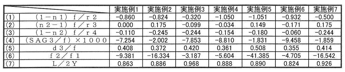
各条件式に対応する実施例の値を表8にまとめて示す。
本発明は、明細書に記載の実施例に限定されるものではなく、他の実施例・変形例を含むことは、本明細書に記載された実施例や技術思想から本分野の当業者にとって明らかである。明細書の記載及び実施例は、あくまでも例証を目的としており、本発明の範囲は後述するクレームによって示されている。
B 操作ボタン
D1,D2 表示画面
F IRカットフィルタ
L1 第1レンズ
L2 第2レンズ
L3 第3レンズ
LN 撮像レンズ
LU 撮像装置
CG カバーガラス
S 開口絞り
IM イメージセンサ
IMa 光電変換部
T 携帯電話機
D1,D2 表示画面
F IRカットフィルタ
L1 第1レンズ
L2 第2レンズ
L3 第3レンズ
LN 撮像レンズ
LU 撮像装置
CG カバーガラス
S 開口絞り
IM イメージセンサ
IMa 光電変換部
T 携帯電話機
Claims (9)
- 物体側から順に開口絞り、第1レンズ、第2レンズからなり、
前記第1レンズは、物体側に凸面、像側に凹面を有する正メニスカスレンズであり、
前記第2レンズは、像側面に近軸凹面を向けた負レンズで、前記像側面は変曲点を持ち周辺が凸形状を有する非球面を備えてなる撮像レンズであって、
以下の条件式を満足することを特徴とする撮像レンズ。
-1.10<(1-n1)f/r2<-0.20 (1)
-0.18<(n2-1)f/r3< 0.18 (2)
-0.25<(1-n2)f/r4<-0.02 (3)
但し、
n1:前記第1レンズのd線に対する屈折率
n2:前記第2レンズのd線に対する屈折率
r2:前記第1レンズ像側面の曲率半径(mm)
r3:前記第2レンズ物体側面の曲率半径(mm)
r4:前記第2レンズ像側面の曲率半径(mm)
f:全系の焦点距離(mm) - 以下の条件式を満足することを特徴とする請求項1に記載の撮像レンズ。
-10.0<(SAG3/f)×1000<0 (4)
ただし、
SAG3:前記第2レンズ物体側面の有効径の7割の位置におけるサグ量 - 第2レンズの物体側面に赤外カットコートを有することを特徴とする請求項1又は2に記載の撮像レンズ。
- 以下の条件式を満足することを特徴とする請求項1~3のいずれか1項に記載の撮像レンズ。
0.30 < d3/f < 0.60 (5)
ただし、
d3:前記第2レンズの軸上厚(mm) - 以下の条件式を満足することを特徴とする請求項1~4のいずれか1項に記載の撮像レンズ。
-20.0 < f2/f1 < -5.0 (6)
ただし、
f1:前記第1レンズの焦点距離(mm)
f2:前記第2レンズの焦点距離(mm) - 前記第2レンズはガラス製であることを特徴とする請求項1~5のいずれか1項に記載の撮像レンズ。
- 前記第2レンズは樹脂製であることを特徴とする請求項1~5のいずれか1項に記載の撮像レンズ。
- 請求項1~7のいずれか1項に記載の撮像レンズと、固体撮像素子とを有し、以下の式を満たすことを特徴とする撮像装置。
L/2Y<1.00 (7)
ただし、
L:前記撮像レンズ全系の最も物体側のレンズ面から像側焦点までの光軸上の距離
2Y:前記固体撮像素子の撮像面対角線長(前記固体撮像素子の矩形実効画素領域の対角線長) - 以下の式を満たすことを特徴とする請求項8に記載の撮像装置。
L/2Y<0.90 (7’)
Priority Applications (2)
| Application Number | Priority Date | Filing Date | Title |
|---|---|---|---|
| JP2013505259A JP5963003B2 (ja) | 2011-10-13 | 2012-10-09 | 撮像レンズ及び撮像装置 |
| CN201280003492.9A CN103229086B (zh) | 2011-10-13 | 2012-10-09 | 摄像透镜以及摄像装置 |
Applications Claiming Priority (2)
| Application Number | Priority Date | Filing Date | Title |
|---|---|---|---|
| JP2011-225645 | 2011-10-13 | ||
| JP2011225645 | 2011-10-13 |
Publications (1)
| Publication Number | Publication Date |
|---|---|
| WO2013054791A1 true WO2013054791A1 (ja) | 2013-04-18 |
Family
ID=48081846
Family Applications (1)
| Application Number | Title | Priority Date | Filing Date |
|---|---|---|---|
| PCT/JP2012/076133 Ceased WO2013054791A1 (ja) | 2011-10-13 | 2012-10-09 | 撮像レンズ及び撮像装置 |
Country Status (3)
| Country | Link |
|---|---|
| JP (1) | JP5963003B2 (ja) |
| CN (1) | CN103229086B (ja) |
| WO (1) | WO2013054791A1 (ja) |
Citations (7)
| Publication number | Priority date | Publication date | Assignee | Title |
|---|---|---|---|---|
| JP2007140006A (ja) * | 2005-11-17 | 2007-06-07 | Matsushita Electric Ind Co Ltd | 撮影レンズおよび2焦点撮影レンズ |
| JP2009098492A (ja) * | 2007-10-18 | 2009-05-07 | Konica Minolta Opto Inc | 撮像レンズ、撮像装置およびデジタル機器 |
| JP2009251516A (ja) * | 2008-04-10 | 2009-10-29 | Komatsulite Mfg Co Ltd | 撮像レンズ |
| JP2010060888A (ja) * | 2008-09-04 | 2010-03-18 | Enplas Corp | 撮像レンズ |
| JP2011145491A (ja) * | 2010-01-14 | 2011-07-28 | Sharp Corp | 撮像レンズ、撮像モジュール、および、携帯情報機器 |
| JP2011248319A (ja) * | 2010-04-28 | 2011-12-08 | Sharp Corp | 撮像レンズおよび撮像モジュール |
| JP2012032635A (ja) * | 2010-07-30 | 2012-02-16 | Sharp Corp | 撮像レンズおよび撮像モジュール |
Family Cites Families (3)
| Publication number | Priority date | Publication date | Assignee | Title |
|---|---|---|---|---|
| TWI341397B (en) * | 2007-05-07 | 2011-05-01 | Largan Precision Co Ltd | Optical lens system for taking image |
| JP5413738B2 (ja) * | 2009-06-26 | 2014-02-12 | コニカミノルタ株式会社 | 撮像レンズ、撮像装置及び携帯端末 |
| CN102236155A (zh) * | 2010-04-28 | 2011-11-09 | 夏普株式会社 | 摄像镜头及摄像模块 |
-
2012
- 2012-10-09 JP JP2013505259A patent/JP5963003B2/ja active Active
- 2012-10-09 CN CN201280003492.9A patent/CN103229086B/zh active Active
- 2012-10-09 WO PCT/JP2012/076133 patent/WO2013054791A1/ja not_active Ceased
Patent Citations (7)
| Publication number | Priority date | Publication date | Assignee | Title |
|---|---|---|---|---|
| JP2007140006A (ja) * | 2005-11-17 | 2007-06-07 | Matsushita Electric Ind Co Ltd | 撮影レンズおよび2焦点撮影レンズ |
| JP2009098492A (ja) * | 2007-10-18 | 2009-05-07 | Konica Minolta Opto Inc | 撮像レンズ、撮像装置およびデジタル機器 |
| JP2009251516A (ja) * | 2008-04-10 | 2009-10-29 | Komatsulite Mfg Co Ltd | 撮像レンズ |
| JP2010060888A (ja) * | 2008-09-04 | 2010-03-18 | Enplas Corp | 撮像レンズ |
| JP2011145491A (ja) * | 2010-01-14 | 2011-07-28 | Sharp Corp | 撮像レンズ、撮像モジュール、および、携帯情報機器 |
| JP2011248319A (ja) * | 2010-04-28 | 2011-12-08 | Sharp Corp | 撮像レンズおよび撮像モジュール |
| JP2012032635A (ja) * | 2010-07-30 | 2012-02-16 | Sharp Corp | 撮像レンズおよび撮像モジュール |
Also Published As
| Publication number | Publication date |
|---|---|
| CN103229086A (zh) | 2013-07-31 |
| CN103229086B (zh) | 2015-09-30 |
| JPWO2013054791A1 (ja) | 2015-03-30 |
| JP5963003B2 (ja) | 2016-08-03 |
Similar Documents
| Publication | Publication Date | Title |
|---|---|---|
| CN201417337Y (zh) | 摄像透镜、及摄像机模块、以及摄像设备 | |
| US9128267B2 (en) | Imaging lens and imaging apparatus including the imaging lens | |
| CN204256243U (zh) | 摄像镜头以及具备该摄像镜头的摄像装置 | |
| JP5839038B2 (ja) | 撮像レンズ及び撮像装置 | |
| US9235029B2 (en) | Imaging lens and imaging apparatus including the imaging lens | |
| CN103718079B (zh) | 广角透镜、摄像光学装置及数码设备 | |
| JP6191628B2 (ja) | 撮影光学系,撮像光学装置及びデジタル機器 | |
| US12044829B2 (en) | Image capturing lens assembly, imaging apparatus and electronic device | |
| WO2013008862A1 (ja) | 撮像レンズ及び撮像装置 | |
| KR102109934B1 (ko) | 촬영 렌즈 및 이를 구비한 촬영 장치 | |
| WO2010047178A1 (ja) | 撮像レンズ及び撮像装置並びに携帯端末 | |
| CN111239971A (zh) | 光学系统、摄像模组及电子装置 | |
| JP5353879B2 (ja) | 撮像レンズ、撮像装置及び携帯端末 | |
| US20250004250A1 (en) | Image capturing system lens assembly, imaging apparatus and electronic device | |
| CN211786312U (zh) | 光学系统、摄像模组及电子装置 | |
| JP6222116B2 (ja) | 撮影光学系,撮像光学装置及びデジタル機器 | |
| WO2013145989A1 (ja) | 撮像レンズ、撮像装置及び携帯端末 | |
| CN110780419A (zh) | 摄像镜头 | |
| JP2013024892A (ja) | 撮像レンズ及び撮像装置 | |
| JP2012230233A (ja) | 撮像レンズ、撮像装置及び携帯端末 | |
| WO2012173026A1 (ja) | 撮像装置用の撮像レンズ及び撮像装置 | |
| CN211577549U (zh) | 光学系统、取像模组及电子设备 | |
| WO2013132915A1 (ja) | 撮像レンズ及び撮像装置 | |
| WO2013018316A1 (ja) | 撮像レンズおよび撮像装置 | |
| CN100439961C (zh) | 成像透镜,成像单元和光学设备 |
Legal Events
| Date | Code | Title | Description |
|---|---|---|---|
| ENP | Entry into the national phase |
Ref document number: 2013505259 Country of ref document: JP Kind code of ref document: A |
|
| 121 | Ep: the epo has been informed by wipo that ep was designated in this application |
Ref document number: 12840682 Country of ref document: EP Kind code of ref document: A1 |
|
| NENP | Non-entry into the national phase |
Ref country code: DE |
|
| 122 | Ep: pct application non-entry in european phase |
Ref document number: 12840682 Country of ref document: EP Kind code of ref document: A1 |