WO2013039073A1 - Aromatic amine derivative and organic electroluminescence element using same - Google Patents
Aromatic amine derivative and organic electroluminescence element using same Download PDFInfo
- Publication number
- WO2013039073A1 WO2013039073A1 PCT/JP2012/073224 JP2012073224W WO2013039073A1 WO 2013039073 A1 WO2013039073 A1 WO 2013039073A1 JP 2012073224 W JP2012073224 W JP 2012073224W WO 2013039073 A1 WO2013039073 A1 WO 2013039073A1
- Authority
- WO
- WIPO (PCT)
- Prior art keywords
- group
- carbon atoms
- substituted
- unsubstituted
- ring
- Prior art date
Links
- 0 Cc1cc(-c2ccccc2*2*N)c2cc1 Chemical compound Cc1cc(-c2ccccc2*2*N)c2cc1 0.000 description 4
- AERLTNUPZDTOLD-UHFFFAOYSA-N C(CC(c(cc1)cc(c2ccccc22)c1[n]2-c1ccccc1)=C1)c2c1c(cccc1)c1[n]2-c(cc1)ccc1C1=NC(c2ccccc2)[N-]C(c2ccccc2)=N1 Chemical compound C(CC(c(cc1)cc(c2ccccc22)c1[n]2-c1ccccc1)=C1)c2c1c(cccc1)c1[n]2-c(cc1)ccc1C1=NC(c2ccccc2)[N-]C(c2ccccc2)=N1 AERLTNUPZDTOLD-UHFFFAOYSA-N 0.000 description 1
- KOHRGAMDOHTQPZ-UHFFFAOYSA-N C(Cc(cc1)ccc1-c(cc1c2c3cccc2)ccc1[n]3-c(cc1)cc2c1[o]c1c2cccc1)C(c1ccccc1)c1cccc2c1cccc2 Chemical compound C(Cc(cc1)ccc1-c(cc1c2c3cccc2)ccc1[n]3-c(cc1)cc2c1[o]c1c2cccc1)C(c1ccccc1)c1cccc2c1cccc2 KOHRGAMDOHTQPZ-UHFFFAOYSA-N 0.000 description 1
- SFKDULYJEPHKIN-UHFFFAOYSA-N CC(CC1c2ccccc2-c2ccccc2C1C)N Chemical compound CC(CC1c2ccccc2-c2ccccc2C1C)N SFKDULYJEPHKIN-UHFFFAOYSA-N 0.000 description 1
- CEWVVNJGDPGADN-UHFFFAOYSA-N CC1(C)c(cc(cc2)N(c(cc3)ccc3-c3ccccc3)c(cc3)ccc3-c(cc3)cc(c4c5cccc4)c3[n]5-c3c4[o]c(cccc5)c5c4ccc3)c2-c2ccccc12 Chemical compound CC1(C)c(cc(cc2)N(c(cc3)ccc3-c3ccccc3)c(cc3)ccc3-c(cc3)cc(c4c5cccc4)c3[n]5-c3c4[o]c(cccc5)c5c4ccc3)c2-c2ccccc12 CEWVVNJGDPGADN-UHFFFAOYSA-N 0.000 description 1
- GSGHPCQRIOIRJQ-UHFFFAOYSA-N CCC(Cc(c(nc1C#N)c(c(nc2C#N)c3nc2C#N)nc1C#N)c3N=C1C#N)=C1C#N Chemical compound CCC(Cc(c(nc1C#N)c(c(nc2C#N)c3nc2C#N)nc1C#N)c3N=C1C#N)=C1C#N GSGHPCQRIOIRJQ-UHFFFAOYSA-N 0.000 description 1
- HBIMXGRAXKJAAP-UHFFFAOYSA-N c(cc1)ccc1-c(cc1)ccc1N(c(cc1)ccc1-c1ccccc1)c(cc1)ccc1-c(cc1c2c3cccc2)ccc1[n]3-c1c2[s]c(cccc3)c3c2ccc1 Chemical compound c(cc1)ccc1-c(cc1)ccc1N(c(cc1)ccc1-c1ccccc1)c(cc1)ccc1-c(cc1c2c3cccc2)ccc1[n]3-c1c2[s]c(cccc3)c3c2ccc1 HBIMXGRAXKJAAP-UHFFFAOYSA-N 0.000 description 1
- HMCGYMAMWPFGHP-UHFFFAOYSA-N c(cc1)ccc1N(c(cc1)ccc1-c(cc1c2ccccc22)ccc1[n]2-c(cc1)ccc1-c1cccc2c1[o]c1ccccc21)c1cccc2c1cccc2 Chemical compound c(cc1)ccc1N(c(cc1)ccc1-c(cc1c2ccccc22)ccc1[n]2-c(cc1)ccc1-c1cccc2c1[o]c1ccccc21)c1cccc2c1cccc2 HMCGYMAMWPFGHP-UHFFFAOYSA-N 0.000 description 1
Images

Classifications
-
- C—CHEMISTRY; METALLURGY
- C07—ORGANIC CHEMISTRY
- C07D—HETEROCYCLIC COMPOUNDS
- C07D405/00—Heterocyclic compounds containing both one or more hetero rings having oxygen atoms as the only ring hetero atoms, and one or more rings having nitrogen as the only ring hetero atom
- C07D405/02—Heterocyclic compounds containing both one or more hetero rings having oxygen atoms as the only ring hetero atoms, and one or more rings having nitrogen as the only ring hetero atom containing two hetero rings
- C07D405/04—Heterocyclic compounds containing both one or more hetero rings having oxygen atoms as the only ring hetero atoms, and one or more rings having nitrogen as the only ring hetero atom containing two hetero rings directly linked by a ring-member-to-ring-member bond
-
- C—CHEMISTRY; METALLURGY
- C07—ORGANIC CHEMISTRY
- C07D—HETEROCYCLIC COMPOUNDS
- C07D405/00—Heterocyclic compounds containing both one or more hetero rings having oxygen atoms as the only ring hetero atoms, and one or more rings having nitrogen as the only ring hetero atom
- C07D405/14—Heterocyclic compounds containing both one or more hetero rings having oxygen atoms as the only ring hetero atoms, and one or more rings having nitrogen as the only ring hetero atom containing three or more hetero rings
-
- H—ELECTRICITY
- H10—SEMICONDUCTOR DEVICES; ELECTRIC SOLID-STATE DEVICES NOT OTHERWISE PROVIDED FOR
- H10K—ORGANIC ELECTRIC SOLID-STATE DEVICES
- H10K85/00—Organic materials used in the body or electrodes of devices covered by this subclass
- H10K85/60—Organic compounds having low molecular weight
- H10K85/615—Polycyclic condensed aromatic hydrocarbons, e.g. anthracene
- H10K85/626—Polycyclic condensed aromatic hydrocarbons, e.g. anthracene containing more than one polycyclic condensed aromatic rings, e.g. bis-anthracene
-
- C—CHEMISTRY; METALLURGY
- C07—ORGANIC CHEMISTRY
- C07D—HETEROCYCLIC COMPOUNDS
- C07D209/00—Heterocyclic compounds containing five-membered rings, condensed with other rings, with one nitrogen atom as the only ring hetero atom
- C07D209/56—Ring systems containing three or more rings
- C07D209/58—[b]- or [c]-condensed
- C07D209/70—[b]- or [c]-condensed containing carbocyclic rings other than six-membered
-
- C—CHEMISTRY; METALLURGY
- C07—ORGANIC CHEMISTRY
- C07D—HETEROCYCLIC COMPOUNDS
- C07D209/00—Heterocyclic compounds containing five-membered rings, condensed with other rings, with one nitrogen atom as the only ring hetero atom
- C07D209/56—Ring systems containing three or more rings
- C07D209/80—[b, c]- or [b, d]-condensed
- C07D209/82—Carbazoles; Hydrogenated carbazoles
- C07D209/86—Carbazoles; Hydrogenated carbazoles with only hydrogen atoms, hydrocarbon or substituted hydrocarbon radicals, directly attached to carbon atoms of the ring system
-
- C—CHEMISTRY; METALLURGY
- C07—ORGANIC CHEMISTRY
- C07D—HETEROCYCLIC COMPOUNDS
- C07D271/00—Heterocyclic compounds containing five-membered rings having two nitrogen atoms and one oxygen atom as the only ring hetero atoms
- C07D271/02—Heterocyclic compounds containing five-membered rings having two nitrogen atoms and one oxygen atom as the only ring hetero atoms not condensed with other rings
- C07D271/10—1,3,4-Oxadiazoles; Hydrogenated 1,3,4-oxadiazoles
- C07D271/107—1,3,4-Oxadiazoles; Hydrogenated 1,3,4-oxadiazoles with two aryl or substituted aryl radicals attached in positions 2 and 5
-
- C—CHEMISTRY; METALLURGY
- C07—ORGANIC CHEMISTRY
- C07D—HETEROCYCLIC COMPOUNDS
- C07D307/00—Heterocyclic compounds containing five-membered rings having one oxygen atom as the only ring hetero atom
- C07D307/77—Heterocyclic compounds containing five-membered rings having one oxygen atom as the only ring hetero atom ortho- or peri-condensed with carbocyclic rings or ring systems
- C07D307/91—Dibenzofurans; Hydrogenated dibenzofurans
-
- C—CHEMISTRY; METALLURGY
- C07—ORGANIC CHEMISTRY
- C07D—HETEROCYCLIC COMPOUNDS
- C07D403/00—Heterocyclic compounds containing two or more hetero rings, having nitrogen atoms as the only ring hetero atoms, not provided for by group C07D401/00
- C07D403/02—Heterocyclic compounds containing two or more hetero rings, having nitrogen atoms as the only ring hetero atoms, not provided for by group C07D401/00 containing two hetero rings
- C07D403/10—Heterocyclic compounds containing two or more hetero rings, having nitrogen atoms as the only ring hetero atoms, not provided for by group C07D401/00 containing two hetero rings linked by a carbon chain containing aromatic rings
-
- C—CHEMISTRY; METALLURGY
- C07—ORGANIC CHEMISTRY
- C07D—HETEROCYCLIC COMPOUNDS
- C07D405/00—Heterocyclic compounds containing both one or more hetero rings having oxygen atoms as the only ring hetero atoms, and one or more rings having nitrogen as the only ring hetero atom
- C07D405/02—Heterocyclic compounds containing both one or more hetero rings having oxygen atoms as the only ring hetero atoms, and one or more rings having nitrogen as the only ring hetero atom containing two hetero rings
- C07D405/10—Heterocyclic compounds containing both one or more hetero rings having oxygen atoms as the only ring hetero atoms, and one or more rings having nitrogen as the only ring hetero atom containing two hetero rings linked by a carbon chain containing aromatic rings
-
- C—CHEMISTRY; METALLURGY
- C07—ORGANIC CHEMISTRY
- C07D—HETEROCYCLIC COMPOUNDS
- C07D409/00—Heterocyclic compounds containing two or more hetero rings, at least one ring having sulfur atoms as the only ring hetero atoms
- C07D409/02—Heterocyclic compounds containing two or more hetero rings, at least one ring having sulfur atoms as the only ring hetero atoms containing two hetero rings
- C07D409/04—Heterocyclic compounds containing two or more hetero rings, at least one ring having sulfur atoms as the only ring hetero atoms containing two hetero rings directly linked by a ring-member-to-ring-member bond
-
- C—CHEMISTRY; METALLURGY
- C07—ORGANIC CHEMISTRY
- C07D—HETEROCYCLIC COMPOUNDS
- C07D409/00—Heterocyclic compounds containing two or more hetero rings, at least one ring having sulfur atoms as the only ring hetero atoms
- C07D409/14—Heterocyclic compounds containing two or more hetero rings, at least one ring having sulfur atoms as the only ring hetero atoms containing three or more hetero rings
-
- C—CHEMISTRY; METALLURGY
- C07—ORGANIC CHEMISTRY
- C07D—HETEROCYCLIC COMPOUNDS
- C07D471/00—Heterocyclic compounds containing nitrogen atoms as the only ring hetero atoms in the condensed system, at least one ring being a six-membered ring with one nitrogen atom, not provided for by groups C07D451/00 - C07D463/00
- C07D471/12—Heterocyclic compounds containing nitrogen atoms as the only ring hetero atoms in the condensed system, at least one ring being a six-membered ring with one nitrogen atom, not provided for by groups C07D451/00 - C07D463/00 in which the condensed system contains three hetero rings
- C07D471/14—Ortho-condensed systems
-
- C—CHEMISTRY; METALLURGY
- C09—DYES; PAINTS; POLISHES; NATURAL RESINS; ADHESIVES; COMPOSITIONS NOT OTHERWISE PROVIDED FOR; APPLICATIONS OF MATERIALS NOT OTHERWISE PROVIDED FOR
- C09B—ORGANIC DYES OR CLOSELY-RELATED COMPOUNDS FOR PRODUCING DYES, e.g. PIGMENTS; MORDANTS; LAKES
- C09B57/00—Other synthetic dyes of known constitution
- C09B57/008—Triarylamine dyes containing no other chromophores
-
- C—CHEMISTRY; METALLURGY
- C09—DYES; PAINTS; POLISHES; NATURAL RESINS; ADHESIVES; COMPOSITIONS NOT OTHERWISE PROVIDED FOR; APPLICATIONS OF MATERIALS NOT OTHERWISE PROVIDED FOR
- C09B—ORGANIC DYES OR CLOSELY-RELATED COMPOUNDS FOR PRODUCING DYES, e.g. PIGMENTS; MORDANTS; LAKES
- C09B57/00—Other synthetic dyes of known constitution
- C09B57/10—Metal complexes of organic compounds not being dyes in uncomplexed form
-
- C—CHEMISTRY; METALLURGY
- C09—DYES; PAINTS; POLISHES; NATURAL RESINS; ADHESIVES; COMPOSITIONS NOT OTHERWISE PROVIDED FOR; APPLICATIONS OF MATERIALS NOT OTHERWISE PROVIDED FOR
- C09K—MATERIALS FOR MISCELLANEOUS APPLICATIONS, NOT PROVIDED FOR ELSEWHERE
- C09K11/00—Luminescent, e.g. electroluminescent, chemiluminescent materials
- C09K11/06—Luminescent, e.g. electroluminescent, chemiluminescent materials containing organic luminescent materials
-
- H—ELECTRICITY
- H05—ELECTRIC TECHNIQUES NOT OTHERWISE PROVIDED FOR
- H05B—ELECTRIC HEATING; ELECTRIC LIGHT SOURCES NOT OTHERWISE PROVIDED FOR; CIRCUIT ARRANGEMENTS FOR ELECTRIC LIGHT SOURCES, IN GENERAL
- H05B33/00—Electroluminescent light sources
- H05B33/12—Light sources with substantially two-dimensional radiating surfaces
- H05B33/14—Light sources with substantially two-dimensional radiating surfaces characterised by the chemical or physical composition or the arrangement of the electroluminescent material, or by the simultaneous addition of the electroluminescent material in or onto the light source
-
- H—ELECTRICITY
- H10—SEMICONDUCTOR DEVICES; ELECTRIC SOLID-STATE DEVICES NOT OTHERWISE PROVIDED FOR
- H10K—ORGANIC ELECTRIC SOLID-STATE DEVICES
- H10K50/00—Organic light-emitting devices
-
- H—ELECTRICITY
- H10—SEMICONDUCTOR DEVICES; ELECTRIC SOLID-STATE DEVICES NOT OTHERWISE PROVIDED FOR
- H10K—ORGANIC ELECTRIC SOLID-STATE DEVICES
- H10K50/00—Organic light-emitting devices
- H10K50/80—Constructional details
-
- H—ELECTRICITY
- H10—SEMICONDUCTOR DEVICES; ELECTRIC SOLID-STATE DEVICES NOT OTHERWISE PROVIDED FOR
- H10K—ORGANIC ELECTRIC SOLID-STATE DEVICES
- H10K85/00—Organic materials used in the body or electrodes of devices covered by this subclass
- H10K85/60—Organic compounds having low molecular weight
- H10K85/615—Polycyclic condensed aromatic hydrocarbons, e.g. anthracene
-
- H—ELECTRICITY
- H10—SEMICONDUCTOR DEVICES; ELECTRIC SOLID-STATE DEVICES NOT OTHERWISE PROVIDED FOR
- H10K—ORGANIC ELECTRIC SOLID-STATE DEVICES
- H10K85/00—Organic materials used in the body or electrodes of devices covered by this subclass
- H10K85/60—Organic compounds having low molecular weight
- H10K85/631—Amine compounds having at least two aryl rest on at least one amine-nitrogen atom, e.g. triphenylamine
- H10K85/633—Amine compounds having at least two aryl rest on at least one amine-nitrogen atom, e.g. triphenylamine comprising polycyclic condensed aromatic hydrocarbons as substituents on the nitrogen atom
-
- H—ELECTRICITY
- H10—SEMICONDUCTOR DEVICES; ELECTRIC SOLID-STATE DEVICES NOT OTHERWISE PROVIDED FOR
- H10K—ORGANIC ELECTRIC SOLID-STATE DEVICES
- H10K85/00—Organic materials used in the body or electrodes of devices covered by this subclass
- H10K85/60—Organic compounds having low molecular weight
- H10K85/631—Amine compounds having at least two aryl rest on at least one amine-nitrogen atom, e.g. triphenylamine
- H10K85/636—Amine compounds having at least two aryl rest on at least one amine-nitrogen atom, e.g. triphenylamine comprising heteroaromatic hydrocarbons as substituents on the nitrogen atom
-
- H—ELECTRICITY
- H10—SEMICONDUCTOR DEVICES; ELECTRIC SOLID-STATE DEVICES NOT OTHERWISE PROVIDED FOR
- H10K—ORGANIC ELECTRIC SOLID-STATE DEVICES
- H10K85/00—Organic materials used in the body or electrodes of devices covered by this subclass
- H10K85/60—Organic compounds having low molecular weight
- H10K85/649—Aromatic compounds comprising a hetero atom
- H10K85/657—Polycyclic condensed heteroaromatic hydrocarbons
- H10K85/6572—Polycyclic condensed heteroaromatic hydrocarbons comprising only nitrogen in the heteroaromatic polycondensed ring system, e.g. phenanthroline or carbazole
-
- H—ELECTRICITY
- H10—SEMICONDUCTOR DEVICES; ELECTRIC SOLID-STATE DEVICES NOT OTHERWISE PROVIDED FOR
- H10K—ORGANIC ELECTRIC SOLID-STATE DEVICES
- H10K85/00—Organic materials used in the body or electrodes of devices covered by this subclass
- H10K85/60—Organic compounds having low molecular weight
- H10K85/649—Aromatic compounds comprising a hetero atom
- H10K85/657—Polycyclic condensed heteroaromatic hydrocarbons
- H10K85/6574—Polycyclic condensed heteroaromatic hydrocarbons comprising only oxygen in the heteroaromatic polycondensed ring system, e.g. cumarine dyes
-
- H—ELECTRICITY
- H10—SEMICONDUCTOR DEVICES; ELECTRIC SOLID-STATE DEVICES NOT OTHERWISE PROVIDED FOR
- H10K—ORGANIC ELECTRIC SOLID-STATE DEVICES
- H10K85/00—Organic materials used in the body or electrodes of devices covered by this subclass
- H10K85/60—Organic compounds having low molecular weight
- H10K85/649—Aromatic compounds comprising a hetero atom
- H10K85/657—Polycyclic condensed heteroaromatic hydrocarbons
- H10K85/6576—Polycyclic condensed heteroaromatic hydrocarbons comprising only sulfur in the heteroaromatic polycondensed ring system, e.g. benzothiophene
-
- C—CHEMISTRY; METALLURGY
- C09—DYES; PAINTS; POLISHES; NATURAL RESINS; ADHESIVES; COMPOSITIONS NOT OTHERWISE PROVIDED FOR; APPLICATIONS OF MATERIALS NOT OTHERWISE PROVIDED FOR
- C09K—MATERIALS FOR MISCELLANEOUS APPLICATIONS, NOT PROVIDED FOR ELSEWHERE
- C09K2211/00—Chemical nature of organic luminescent or tenebrescent compounds
- C09K2211/10—Non-macromolecular compounds
- C09K2211/1018—Heterocyclic compounds
- C09K2211/1025—Heterocyclic compounds characterised by ligands
- C09K2211/1074—Heterocyclic compounds characterised by ligands containing more than three nitrogen atoms as heteroatoms
-
- H—ELECTRICITY
- H10—SEMICONDUCTOR DEVICES; ELECTRIC SOLID-STATE DEVICES NOT OTHERWISE PROVIDED FOR
- H10K—ORGANIC ELECTRIC SOLID-STATE DEVICES
- H10K2101/00—Properties of the organic materials covered by group H10K85/00
- H10K2101/10—Triplet emission
-
- H—ELECTRICITY
- H10—SEMICONDUCTOR DEVICES; ELECTRIC SOLID-STATE DEVICES NOT OTHERWISE PROVIDED FOR
- H10K—ORGANIC ELECTRIC SOLID-STATE DEVICES
- H10K50/00—Organic light-emitting devices
- H10K50/10—OLEDs or polymer light-emitting diodes [PLED]
- H10K50/11—OLEDs or polymer light-emitting diodes [PLED] characterised by the electroluminescent [EL] layers
-
- H—ELECTRICITY
- H10—SEMICONDUCTOR DEVICES; ELECTRIC SOLID-STATE DEVICES NOT OTHERWISE PROVIDED FOR
- H10K—ORGANIC ELECTRIC SOLID-STATE DEVICES
- H10K50/00—Organic light-emitting devices
- H10K50/10—OLEDs or polymer light-emitting diodes [PLED]
- H10K50/14—Carrier transporting layers
- H10K50/15—Hole transporting layers
- H10K50/157—Hole transporting layers between the light-emitting layer and the cathode
-
- H—ELECTRICITY
- H10—SEMICONDUCTOR DEVICES; ELECTRIC SOLID-STATE DEVICES NOT OTHERWISE PROVIDED FOR
- H10K—ORGANIC ELECTRIC SOLID-STATE DEVICES
- H10K85/00—Organic materials used in the body or electrodes of devices covered by this subclass
- H10K85/30—Coordination compounds
- H10K85/341—Transition metal complexes, e.g. Ru(II)polypyridine complexes
- H10K85/342—Transition metal complexes, e.g. Ru(II)polypyridine complexes comprising iridium
-
- H—ELECTRICITY
- H10—SEMICONDUCTOR DEVICES; ELECTRIC SOLID-STATE DEVICES NOT OTHERWISE PROVIDED FOR
- H10K—ORGANIC ELECTRIC SOLID-STATE DEVICES
- H10K85/00—Organic materials used in the body or electrodes of devices covered by this subclass
- H10K85/60—Organic compounds having low molecular weight
- H10K85/631—Amine compounds having at least two aryl rest on at least one amine-nitrogen atom, e.g. triphenylamine
Definitions
- the present invention relates to an aromatic amine derivative and an organic electroluminescence element (hereinafter sometimes referred to as an organic EL element).
- Organic electroluminescence (EL) elements are promising for use as solid-state, inexpensive, large-area full-color display elements, and many developments have been made.
- an organic EL element is composed of a light emitting layer and a pair of counter electrodes sandwiching the layer. When a voltage is applied between both electrodes, electrons from the cathode side and holes from the anode side are injected into the light-emitting layer, and the injected electrons and holes recombine in the light-emitting layer, generating an excited state and being excited. When the state returns to the ground state, energy is emitted as light.
- a phosphorescent organic EL element that uses a phosphorescent organic material for the light emitting layer of the organic EL element has been proposed.
- This phosphorescent organic EL element achieves high luminous efficiency by utilizing the singlet excited state and the triplet excited state of the phosphorescent organic material.
- electrons and holes are recombined in the organic EL element, it is considered that singlet excitons and triplet excitons are generated at a ratio of 1: 3 due to the difference in spin multiplicity. If a light emitting material is used, it can be considered that the light emission efficiency is 3 to 4 times that of an element using only a fluorescent light emitting material.
- Improvement of the luminous efficiency and extension of the lifetime of organic EL elements are important issues that lead to lower power consumption and higher durability of the display, and further improvements are required.
- various studies have been made in order to improve the light emission efficiency and the device life of an organic EL device using a phosphorescent light emitting material.
- Patent Document 1 discloses a derivative having a biscarbazole skeleton.
- Patent Documents 2 and 3 disclose derivatives having a monoamino-carbazole skeleton, each of which has a pyrene residue and an anthracene residue as essential, for use as a fluorescent host.
- An object of the present invention is to provide an organic EL element having a high luminous efficiency and a long lifetime, and an organic EL material that realizes the organic EL element.
- L 1 represents a single bond, a substituted or unsubstituted arylene group having 6 to 30 ring carbon atoms, or a substituted or unsubstituted heteroarylene group having 5 to 30 ring carbon atoms.
- L2 represents a single bond, a substituted or unsubstituted heteroarylene group having 5 to 30 ring carbon atoms, or a substituted or unsubstituted arylene group, and the arylene group includes a phenylene group, a biphenylylene group, a terphenylylene group, a naphthylene.
- Ar 1 and Ar 2 each independently represents a substituted or unsubstituted aryl group having 6 to 30 ring carbon atoms or a substituted or unsubstituted heteroaryl group having 5 to 30 ring carbon atoms.
- R 1 and R 2 are each independently a fluorine atom, a cyano group, a substituted or unsubstituted alkyl group having 1 to 20 carbon atoms, a substituted or unsubstituted cycloalkyl group having 3 to 20 carbon atoms, substituted or unsubstituted An alkoxy group having 1 to 20 carbon atoms, a substituted or unsubstituted haloalkyl group having 1 to 20 carbon atoms, a substituted or unsubstituted haloalkoxy group having 1 to 20 carbon atoms, a substituted or unsubstituted 1 to 10 carbon atoms An alkylsilyl group, a substituted or unsubstituted arylsilyl group having 6 to 30 carbon atoms, a substituted or unsubstituted aralkyl group having 7 to 30 carbon atoms, a substituted or unsubstituted aryl group having 6 to 30 ring carbon
- a represents an integer of 0 to 3.
- b represents an integer of 0 to 4.
- Q is a group represented by the following formula (a). ] [In Formula (a), X represents an oxygen atom or a sulfur atom.
- R 3 and R 4 are each independently a fluorine atom, a cyano group, a substituted or unsubstituted alkyl group having 1 to 20 carbon atoms, a substituted or unsubstituted cycloalkyl group having 3 to 20 carbon atoms, substituted or unsubstituted An alkoxy group having 1 to 20 carbon atoms, a substituted or unsubstituted haloalkyl group having 1 to 20 carbon atoms, a substituted or unsubstituted haloalkoxy group having 1 to 20 carbon atoms, a substituted or unsubstituted 1 to 10 carbon atoms An alkylsilyl group, a substituted or unsubstituted aryls
- R 14 and R 15 are each independently a hydrogen atom, a substituted or unsubstituted alkyl group having 1 to 20 carbon atoms, a substituted or unsubstituted cycloalkyl group having 3 to 20 carbon atoms, a substituted or unsubstituted carbon number.
- k 1 to k 3 represent integers of 0 to 4. ] 6).
- a material for an organic electroluminescence device comprising the aromatic amine derivative according to any one of 1 to 10 above, 12
- An organic electroluminescence device comprising an anode, a cathode, and an organic thin film layer comprising one or more layers between the anode and the cathode, wherein the organic thin film layer includes a light emitting layer, wherein at least one of the organic thin film layers is
- An organic electroluminescence device comprising the aromatic amine derivative according to any one of 1 to 10 above, 14 14.
- the organic electroluminescence device wherein the acceptor material is represented by the following formula (10):
- R 21 to R 26 are each independently a cyano group, —CONH 2 , carboxy group, or —COOR 27 (R 27 is an alkyl group having 1 to 20 carbon atoms or 3 to 20 carbon atoms) Or one or more pairs of R 21 and R 22 , R 23 and R 24 , and R 25 and R 26 are bonded to each other to form —CO—O—CO— Forming the indicated group.) 17.
- the organic electroluminescent device according to any one of the above 13 to 16, wherein the light emitting layer contains a phosphorescent material, and 18.
- the organic electroluminescence device according to 17 above, wherein the phosphorescent material is an orthometalated complex of iridium (Ir), osmium (Os) or platinum (Pt) metal, Is to provide.
- Ir iridium
- Os osmium
- Pt platinum
- an organic EL element having high luminous efficiency and a long lifetime and an organic EL material that realizes the organic EL element.
- FIG. 1 is a schematic cross-sectional view showing an example of the organic EL element of the present invention.
- carbon number ab in the expression “substituted or unsubstituted X group having carbon number ab” represents the carbon number when X group is unsubstituted, The carbon number of the substituent when the group is substituted is not included.
- X group having a substituted or unsubstituted ring-forming carbon number a to b and “X group having a substituted or unsubstituted ring-forming carbon atom number a to b”, where a to b are carbon atoms contained in the ring. It represents the number of atoms or the number of atoms, and does not include the number of carbon atoms or atoms of the substituent.
- Aromatic amine derivative The aromatic amine derivative of the present invention is represented by the following formula (1).
- L 1 in the formula (1) is a single bond, a substituted or unsubstituted arylene group having 6 to 30, preferably 6 to 24, more preferably 6 to 12, or a substituted or unsubstituted ring-forming carbon. It represents a heteroarylene group of 5-30, preferably 5-24, more preferably 5-12.
- L 2 in the formula (1) is a single bond, a substituted or unsubstituted heteroarylene group having 5 to 30, preferably 5 to 24, more preferably 5 to 12 ring-forming carbon atoms, or a substituted or unsubstituted arylene group
- the arylene group is selected from a phenylene group, a biphenylylene group, a terphenylylene group, a naphthylene group, a phenanthrylene group, a chrysenylene group, a peryleneylene group, and a fluorenylene group.
- Ar 1 and Ar 2 in the formula (1) are each independently a substituted or unsubstituted aryl group having 6 to 30, preferably 6 to 24, more preferably 6 to 12 ring-forming carbon atoms, or substituted or unsubstituted.
- R 1 and R 2 in the formula (1) are each independently a fluorine atom, a cyano group, a substituted or unsubstituted alkyl group having 1 to 20, preferably 1 to 10, more preferably 1 to 5 carbon atoms, substituted Or an unsubstituted cycloalkyl group having 3 to 20 carbon atoms, preferably 3 to 10 carbon atoms, more preferably 3 to 6 carbon atoms, a substituted or unsubstituted carbon atom having 1 to 20 carbon atoms, preferably 1 to 10 carbon atoms, more preferably 1 to 5 carbon atoms.
- a represents an integer of 0 to 3, preferably an integer of 0 to 2, particularly preferably 0.
- b represents an integer of 0 to 4, preferably an integer of 0 to 2, particularly preferably 0.
- Q in the formula (1) is a group represented by the following formula (a).
- X in the formula (a) represents an oxygen atom or a sulfur atom.
- R 3 and R 4 in formula (a) are each independently a fluorine atom, a cyano group, a substituted or unsubstituted alkyl group having 1 to 20, preferably 1 to 10, more preferably 1 to 5 carbon atoms, substituted Or an unsubstituted cycloalkyl group having 3 to 20 carbon atoms, preferably 3 to 10 carbon atoms, more preferably 3 to 6 carbon atoms, a substituted or unsubstituted carbon atom having 1 to 20 carbon atoms, preferably 1 to 10 carbon atoms, more preferably 1 to 5 carbon atoms.
- c represents an integer of 0 to 3, preferably an integer of 0 to 2, particularly preferably 0.
- d represents an integer of 0 to 4, preferably an integer of 0 to 2, particularly preferably 0.
- the formula (a) represented by Q is preferably represented by the following formula (a-1) or (a-2), and particularly preferably represented by the formula (a-2).
- R 3 , R 4 , c, d, and X have the same meanings as in the formula (a).
- Examples of the arylene group represented by L 1 include benzene, naphthalene, phenanthrene, biphenyl, terphenyl (including isomer), quarterphenyl (including isomer), fluoranthene, triphenylene, 9,9-dimethylfluorene, benzo [C] Aromatics selected from phenanthrene, benzo [a] triphenylene, naphtho [1,2-c] phenanthrene, naphtho [1,2-a] triphenylene, dibenzo [a, c] triphenylene, and benzo [b] fluoranthene And divalent residues of the compound, preferably 1,4-phenylene group, 1,3-phenylene group, biphenyl-4,4′-diyl group, biphenyl-3,3′-diyl group, biphenyl- 3,4'-diyl group, p-terphenyl-4,4 "-diyl group, m-terphenyl
- heteroarylene group represented by L 1 examples include those containing at least one, preferably 1 to 3 heteroatoms selected from a nitrogen atom, an oxygen atom, and a sulfur atom. Specific examples thereof include: Pyrrole, furan, thiophene, pyridine, pyridazine, pyrimidine, pyrazine, triazine, imidazole, oxazole, thiazole, pyrazole, isoxazole, isothiazole, oxadiazole, thiadiazole, triazole, indoline, isoindoline, benzofuran, isobenzofuran, benzothiophene , Indolizine, quinolidine, quinoline, isoquinoline, cinnoline, phthalazine, quinazoline, quinoxaline, benzimidazole, benzoxazole, benzthiazole, indazole, benzisoxazol , Divalent residues of
- the arylene group represented by L 2 is preferably 1,4-phenylene group, 1,3-phenylene group, biphenyl-4,4′-diyl group, biphenyl-3,4′-diyl group, biphenyl-3,3 '-Diyl group, naphthalene-2,6-diyl group, naphthalene-1,4-diyl group, naphthalene-1,5-diyl group, phenanthrene-2,7-diyl group, and 9,9-dimethylfluorene-2 , 7-diyl group, particularly preferably 1,4-phenylene group, biphenyl-4,4′-diyl group, and 9,9-dimethylfluorene-2,7-diyl group.
- the heteroarylene group represented by L 2 is defined in the same manner as the heteroarylene group represented by L 1 and preferred embodiments thereof.
- Examples of the aryl group represented by Ar 1 and Ar 2 include a phenyl group, a naphthyl group, a phenanthryl group, a biphenylyl group, a terphenylyl group, a quaterphenylyl group, a fluoranthenyl group, a triphenylenyl group, 9,9-dimethylfluorene.
- heteroaryl group represented by Ar 1 and Ar 2 are preferably those containing at least one, preferably 1 to 3 heteroatoms selected from a nitrogen atom, an oxygen atom, and a sulfur atom.
- Examples of the alkyl group represented by R 1 to R 4 include methyl group, ethyl group, n-propyl group, isopropyl group, n-butyl group, s-butyl group, isobutyl group, t-butyl group, and n-pentyl.
- Examples of the cycloalkyl group represented by R 1 to R 4 include a cyclopropyl group, a cyclobutyl group, a cyclopentyl group, a cyclohexyl group, and a cyclooctyl group, and a cyclopentyl group and a cyclohexyl group are preferable.
- Examples of the haloalkyl group represented by R 1 to R 4 include a chloromethyl group, a 1-chloromethyl group, a 2-chloroethyl group, a 2-chloroisobutyl, a 1,2-dichloroethyl group, and a 1,3-dichloroisopropyl group.
- the alkoxy group represented by R 1 to R 4 is represented by —OX 1
- X 1 is a group selected from the alkyl group represented by R 1 to R 4 and a preferred alkyl group.
- the haloalkoxy group represented by R 1 to R 4 is a group represented by —OX 2
- X 2 is a group selected from the haloalkyl group represented by R 1 to R 4 and a preferred haloalkyl group.
- alkylsilyl group represented by the R 1 ⁇ R 4 are, -SiH 2 R, -SiHR 2, or -SiR 3 (R is a group selected from alkyl groups and preferred alkyl groups represented by the R 1 ⁇ R 4 And 2 or 3 Rs may be the same or different), and are preferably a trimethylsilyl group, a triethylsilyl group, or a t-butyldimethylsilyl group.
- Examples of the aryl group represented by R 1 to R 4 include phenyl, naphthyl, phenanthryl, biphenylyl, terphenylyl, quarterphenylyl, fluoranthenyl, triphenylenyl, 9,9-dimethylfluore.
- aryl silyl group represented by the R 1 ⁇ R 4 are, -SiH 2 Ar, -SiHAr 2, or -SiAr 3 (Ar is a group selected from aryl and preferred aryl groups represented by R 1 ⁇ R 4 Yes, 2 or 3 Ars may be the same or different), and is preferably a triphenylsilyl group.
- Examples of the aralkyl group represented by R 1 to R 4 include a benzyl group, a 1-phenylethyl group, a 2-phenylethyl group, a 1-phenylisopropyl group, a 2-phenylisopropyl group, and a phenyl-t-butyl group. And preferred are a benzyl group, a 1-phenylethyl group, and a 2-phenylethyl group.
- the heteroaryl group represented by R 1 to R 4 is preferably one containing at least one, preferably 1 to 3 heteroatoms selected from a nitrogen atom, an oxygen atom and a sulfur atom.
- the divalent groups formed by bonding of adjacent R 1 , adjacent R 2 , adjacent R 3 , and adjacent R 4 to each other include a butane-1,4-diyl group, 1, 3 -Butadiene-1,4-diyl group and the like.
- Ring structures formed by R 1 , R 2 , R 3 , and R 4 bonded together with the ring-forming carbon of the benzene ring include aromatic hydrocarbon rings having 6 to 30 ring carbon atoms, ring formation Examples thereof include an aromatic heterocycle having 5 to 30 carbon atoms and a ring in which a part of the aromatic hydrocarbon ring or aromatic heterocycle is saturated.
- At least one of L 1 and L 2 is preferably a single bond or a linking group represented by any of the following formulas (b-1) to (b-3).
- the linking group represented is particularly preferred.
- R 11 to R 13 are each independently a fluorine atom, a cyano group, a substituted or unsubstituted alkyl group having 1 to 20, preferably 1 to 10, more preferably 1 to 5 carbon atoms, a substituted or unsubstituted carbon.
- a haloalkoxy group a substituted or unsubstituted alkylsilyl group having 1 to 10 carbon atoms, preferably 1 to 5 carbon atoms, more preferably 1 to 3 carbon atoms, a substituted or unsubstituted carbon atom number 6 to 30 carbon atoms, preferably 6 to 2 carbon atoms; 4, more preferably an arylsilyl group having 6 to 18 carbon atoms, a substituted or unsubstituted carbon number of 7 to 30, preferably 7 to 25, more preferably 7 to 13 carbon atoms, a substituted or unsubstituted ring carbon number of 6 -30, preferably 6-24, more preferably 6-12 aryl group, or a substituted or unsubstituted heteroaryl group having 5-30, preferably 5-24, more preferably 5-12 ring-forming carbon atoms.
- Each of adjacent R 11 , adjacent R 12 , and adjacent R 13 may be bonded to each other to form a ring structure together with the ring
- Each of the alkyl group, cycloalkyl group, alkoxy group, haloalkyl group, haloalkoxy group, alkylsilyl group, arylsilyl group, aralkyl group, aryl group, and heteroaryl group represented by R 11 to R 13 is the above R 1.
- the definition of each corresponding group represented by ⁇ R 4 is the same.
- Divalent groups formed by bonding of adjacent R 11 , adjacent R 12 , and adjacent R 13 to each other include butane-1,4-diyl group, 1,3-butadiene-1,4 -Diyl groups and the like.
- Examples of the ring structure formed by R 11 , R 12 and R 13 bonded together with the ring-forming carbon of the benzene ring include aromatic hydrocarbon rings having 6 to 30 ring carbon atoms, 30 aromatic heterocycles, and rings saturated with a part of the aromatic hydrocarbon ring or aromatic heterocycle.
- Each of k 1 to k 3 represents an integer of 0 to 4, preferably an integer of 0 to 2, particularly preferably 0. When each of k 1 to k 3 is 0, it means that substituents R 11 , R 12 and R 13 are not present.
- R 14 and R 15 are each independently a hydrogen atom, a substituted or unsubstituted alkyl group having 1 to 20, preferably 1 to 10, more preferably 1 to 5 carbon atoms, a substituted or unsubstituted carbon group having 3 to 20, preferably 3 to 10, more preferably 3 to 6 cycloalkyl groups, substituted or unsubstituted haloalkyl groups having 1 to 20, preferably 1 to 10, more preferably 1 to 5 carbon atoms, substituted or unsubstituted An aralkyl group having 7 to 30 carbon atoms, preferably 7 to 25 carbon atoms, more preferably 7 to 13 carbon atoms, a substituted or unsubstituted aryl group having 6 to 30 ring carbon atoms, preferably 6 to 24 carbon atoms, more preferably 6 to 12 carbon atoms. Or a substituted or unsubstituted heteroaryl group having 5 to 30, preferably 5 to 24, more preferably 5 to 12 ring-forming carbon atoms.
- Each of the alkyl group, cycloalkyl group, haloalkyl group, aralkyl group, aryl group and heteroaryl group represented by R 14 and R 15 is as defined for the corresponding groups represented by R 1 to R 4 .
- the phenylene group represented by the formula (b-1) includes a 1,2-phenylene group, a 1,3-phenylene group, and a 1,4-phenylene group, and a 1,4-phenylene group is particularly preferable.
- the biphenyldiyl group represented by the formula (b-2) is, for example, a biphenyl-4,4′-diyl group, a biphenyl-3,4′-diyl group, a biphenyl-3,3′-diyl group, A -4,4'-diyl group is particularly preferred.
- Examples of the fluorenediyl group represented by the formula (b-3) include 9,9-dimethylfluorene-2,7-diyl group, 9,9-diphenylfluorene-2,7-diyl group, 9-methyl- It is a 9-phenylfluorene-2,7-diyl group, and a 9,9-dimethylfluorene-2,7-diyl group is particularly preferable.
- the aromatic amine derivative according to the present invention is preferably represented by the following formula (1-1).
- L 1 , L 2 , Ar 1 , Ar 2 , R 1 , R 2 , a, b, and Q are as defined above.
- the optional substituent in the case of “substituted or unsubstituted” described above and below is a fluorine atom, a cyano group, an alkyl group having 1 to 20 carbon atoms (preferably 1 to 5), and 3 to 20 carbon atoms (preferably 5 carbon atoms).
- a cycloalkyl group an alkoxy group having 1 to 20 carbon atoms (preferably 1 to 5), a haloalkyl group having 1 to 20 carbon atoms (preferably 1 to 5), a 1 to 20 carbon atoms (preferably 1 to 5) a haloalkoxy group, an alkylsilyl group having 1 to 10 carbon atoms (preferably 1 to 5), an aryl group having 6 to 30 ring carbon atoms (preferably 6 to 18 carbon atoms), a ring carbon atom number 6 to 30 ( Preferably 6-18) aryloxy group, 6-30 carbon atoms (preferably 6-18) arylsilyl group, 7-30 carbon atoms (preferably 7-20) aralkyl group, and 5 ring atoms.
- ⁇ 30 (preferred Can be mentioned heteroaryl group of from 5 to 18).
- the organic EL device of the present invention has an organic thin film layer composed of one or more layers between a cathode and an anode.
- the organic thin film layer includes a light emitting layer, and at least one of the organic thin film layers includes the above-described aromatic amine derivative of the present invention.
- the aromatic amine derivative of the present invention is contained in at least one of the organic thin film layers of the organic EL element of the present invention, it can be expected that the organic EL element has high luminous efficiency and long life.
- Examples of the organic thin film layer containing the aromatic amine derivative of the present invention include, but are not limited to, a hole transport layer, a light emitting layer, a space layer, and a barrier layer.
- the aromatic amine derivative of the present invention is particularly preferably contained in the hole transport layer.
- the light emitting layer preferably contains a fluorescent light emitting material or a phosphorescent light emitting material, and particularly preferably contains a phosphorescent light emitting material.
- the organic EL element of the present invention may be a fluorescent or phosphorescent monochromatic light emitting element, a fluorescent / phosphorescent hybrid white light emitting element, or a simple type having a single light emitting unit.
- a tandem type having a plurality of light emitting units may be used.
- the “light emitting unit” refers to a minimum unit that includes one or more organic thin film layers, one of which is a light emitting layer, and can emit light by recombination of injected holes and electrons. .
- typical element configurations of simple organic EL elements include the following element configurations.
- Anode / light emitting unit / cathode The above light emitting unit may be a laminated type having a plurality of phosphorescent light emitting layers and fluorescent light emitting layers. In that case, the light emitting unit is generated by a phosphorescent light emitting layer between the light emitting layers. In order to prevent the excitons from diffusing into the fluorescent light emitting layer, a space layer may be provided. A typical layer structure of the light emitting unit is shown below.
- A Hole transport layer / light emitting layer (/ electron transport layer)
- B Hole transport layer / first phosphorescent light emitting layer / second phosphorescent light emitting layer (/ electron transport layer)
- C Hole transport layer / phosphorescent layer / space layer / fluorescent layer (/ electron transport layer)
- D Hole transport layer / first phosphorescent light emitting layer / second phosphorescent light emitting layer / space layer / fluorescent light emitting layer (/ electron transport layer)
- E Hole transport layer / first phosphorescent light emitting layer / space layer / second phosphorescent light emitting layer / space layer / fluorescent light emitting layer (/ electron transport layer)
- F Hole transport layer / phosphorescent layer / space layer / first fluorescent layer / second fluorescent layer (/ electron transport layer)
- Each phosphorescent or fluorescent light-emitting layer may have a different emission color.
- a layer structure such as an electron transport layer can be used.
- An electron barrier layer may be appropriately provided between each light emitting layer and the hole transport layer or space layer.
- a hole blocking layer may be appropriately provided between each light emitting layer and the electron transport layer.
- the following element structure can be mentioned as a typical element structure of a tandem type organic EL element.
- the intermediate layer is generally called an intermediate electrode, an intermediate conductive layer, a charge generation layer, an electron extraction layer, a connection layer, or an intermediate insulating layer, and has electrons in the first light emitting unit and holes in the second light emitting unit.
- a known material structure to be supplied can be used.
- FIG. 1 shows a schematic configuration of an example of the organic EL element of the present invention.
- the organic EL element 1 includes a substrate 2, an anode 3, a cathode 4, and a light emitting unit 10 disposed between the anode 3 and the cathode 4.
- the light emitting unit 10 includes a light emitting layer 5 including at least one phosphorescent light emitting layer including a phosphorescent host material and a phosphorescent dopant.
- a hole transport layer 6 or the like may be formed between the light emitting layer 5 and the anode 3, and an electron transport layer 7 or the like may be formed between the light emitting layer 5 and the cathode 4.
- an electron barrier layer may be provided on the anode 3 side of the light emitting layer 5, and a hole barrier layer may be provided on the cathode 4 side of the light emitting layer 5.
- a host combined with a fluorescent dopant is referred to as a fluorescent host
- a host combined with a phosphorescent dopant is referred to as a phosphorescent host.
- the fluorescent host and the phosphorescent host are not distinguished only by the molecular structure. That is, the phosphorescent host means a material constituting a phosphorescent light emitting layer containing a phosphorescent dopant, and does not mean that it cannot be used as a material constituting a fluorescent light emitting layer. The same applies to the fluorescent host.
- the organic EL device of the present invention is produced on a light-transmitting substrate.
- the light-transmitting substrate is a substrate that supports the organic EL element, and is preferably a smooth substrate having a light transmittance in the visible region of 400 nm to 700 nm of 50% or more.
- a glass plate, a polymer plate, etc. are mentioned.
- the glass plate include those using soda lime glass, barium / strontium-containing glass, lead glass, aluminosilicate glass, borosilicate glass, barium borosilicate glass, quartz and the like as raw materials.
- the polymer plate include those using polycarbonate, acrylic, polyethylene terephthalate, polyether sulfide, polysulfone and the like as raw materials.
- the anode of the organic EL element plays a role of injecting holes into the hole transport layer or the light emitting layer, and it is effective to use one having a work function of 4.5 eV or more.
- Specific examples of the anode material include indium tin oxide alloy (ITO), tin oxide (NESA), indium zinc oxide, gold, silver, platinum, copper, and the like.
- the anode can be produced by forming a thin film of these electrode materials by a method such as vapor deposition or sputtering. When light emitted from the light emitting layer is extracted from the anode, it is preferable that the transmittance of light in the visible region of the anode is greater than 10%.
- the sheet resistance of the anode is preferably several hundred ⁇ / ⁇ or less.
- the film thickness of the anode depends on the material, but is usually selected in the range of 10 nm to 1 ⁇ m, preferably 10 nm to 200 nm.
- the cathode plays a role of injecting electrons into the electron injection layer, the electron transport layer, or the light emitting layer, and is preferably formed of a material having a small work function.
- the cathode material is not particularly limited, and specifically, indium, aluminum, magnesium, magnesium-indium alloy, magnesium-aluminum alloy, aluminum-lithium alloy, aluminum-scandium-lithium alloy, magnesium-silver alloy and the like can be used.
- the cathode can be produced by forming a thin film by a method such as vapor deposition or sputtering. Moreover, you may take out light emission from the cathode side as needed.
- Light-emitting layer An organic layer having a light-emitting function, and when a doping system is employed, includes a host material and a dopant material.
- the host material mainly has a function of encouraging recombination of electrons and holes and confining excitons in the light emitting layer, and the dopant material efficiently emits excitons obtained by recombination. It has a function.
- the host material mainly has a function of confining excitons generated by the dopant in the light emitting layer.
- the light emitting layer employs, for example, a double host (also referred to as a host / cohost) that adjusts the carrier balance in the light emitting layer by combining an electron transporting host and a hole transporting host. Also good. Moreover, you may employ
- the above light-emitting layer is a laminate in which a plurality of light-emitting layers are stacked, so that electrons and holes are accumulated at the light-emitting layer interface, and the recombination region is concentrated at the light-emitting layer interface to improve quantum efficiency. Can do.
- the ease of injecting holes into the light emitting layer may be different from the ease of injecting electrons, and the hole transport ability and electron transport ability expressed by the mobility of holes and electrons in the light emitting layer may be different. May be different.
- the light emitting layer can be formed by a known method such as a vapor deposition method, a spin coating method, or an LB method.
- the light emitting layer can also be formed by thinning a solution obtained by dissolving a binder such as a resin and a material compound in a solvent by a spin coating method or the like.
- the light emitting layer is preferably a molecular deposited film.
- the molecular deposited film is a thin film formed by deposition from a material compound in a gas phase state or a film formed by solidifying from a material compound in a solution state or a liquid phase state.
- the thin film (molecular accumulation film) formed by the LB method can be classified by the difference in the aggregation structure and the higher-order structure, and the functional difference resulting therefrom.
- the phosphorescent dopant (phosphorescent material) that forms the light emitting layer is a compound that can emit light from the triplet excited state, and is not particularly limited as long as it emits light from the triplet excited state, but Ir, Pt, Os, Au, Cu, An organometallic complex containing at least one metal selected from Re and Ru and a ligand is preferable.
- the ligand preferably has an ortho metal bond.
- a metal complex containing a metal atom selected from Ir, Os and Pt is preferred in that the phosphorescent quantum yield is high and the external quantum efficiency of the light emitting device can be further improved, and an iridium complex, an osmium complex, or a platinum complex.
- iridium complexes and platinum complexes are more preferable, and orthometalated iridium complexes are particularly preferable.
- the content of the phosphorescent dopant in the light emitting layer is not particularly limited and may be appropriately selected depending on the intended purpose. For example, it is preferably 0.1 to 70% by mass, more preferably 1 to 30% by mass. If the phosphorescent dopant content is 0.1% by mass or more, sufficient light emission can be obtained, and if it is 70% by mass or less, concentration quenching can be avoided.
- the phosphorescent host is a compound having a function of efficiently emitting the phosphorescent dopant by efficiently confining the triplet energy of the phosphorescent dopant in the light emitting layer.
- the aromatic amine derivative of the present invention is useful as a phosphorescent host, compounds other than the aromatic amine derivative of the present invention can be appropriately selected as the phosphorescent host according to the above-mentioned purpose.
- the aromatic amine derivative of the present invention and other compounds may be used in combination as a phosphorescent host material in the same light emitting layer, and when there are a plurality of light emitting layers, the phosphorescent host material of one of the light emitting layers
- the aromatic amine derivative of the present invention may be used, and a compound other than the aromatic amine derivative of the present invention may be used as the phosphorescent host material of another light emitting layer.
- the aromatic amine derivative of the present invention can be used in an organic layer other than the light emitting layer. In that case, a compound other than the aromatic amine derivative of the present invention may be used as the phosphorescent host of the light emitting layer. Good.
- compounds other than the aromatic amine derivative of the present invention and suitable as a phosphorescent host include carbazole derivatives, triazole derivatives, oxazole derivatives, oxadiazole derivatives, imidazole derivatives, polyarylalkane derivatives, pyrazoline derivatives, pyrazolones.
- phenylenediamine derivatives phenylenediamine derivatives, arylamine derivatives, amino-substituted chalcone derivatives, styrylanthracene derivatives, fluorenone derivatives, hydrazone derivatives, stilbene derivatives, silazane derivatives, aromatic tertiary amine compounds, styrylamine compounds, aromatic dimethylidene compounds, porphyrins Compounds, anthraquinodimethane derivatives, anthrone derivatives, diphenylquinone derivatives, thiopyran dioxide derivatives, carbodiimide derivatives, fluorenylidene derivatives Typical examples include metal complexes of heterocyclic tetracarboxylic acid anhydrides such as benzene derivatives, distyrylpyrazine derivatives, naphthaleneperylene, phthalocyanine derivatives, 8-quinolinol derivatives, metal phthalocyanines, benzoxazole and
- polysilane compounds poly (N-vinylcarbazole) derivatives, aniline copolymers, thiophene oligomers, conductive polymer oligomers such as polythiophene, polythiophene derivatives, polyphenylene derivatives, polyphenylene vinylene derivatives, polyfluorene derivatives, etc.
- thiophene oligomers conductive polymer oligomers such as polythiophene, polythiophene derivatives, polyphenylene derivatives, polyphenylene vinylene derivatives, polyfluorene derivatives, etc.
- conductive polymer oligomers such as polythiophene, polythiophene derivatives, polyphenylene derivatives, polyphenylene vinylene derivatives, polyfluorene derivatives, etc.
- a phosphorescent host may be used independently and may use 2 or more types together. Specific examples include the following compounds.
- the thickness of the light emitting layer is preferably 5 to 50 nm, more preferably 7 to 50 nm, and still more preferably 10 to 50 nm.
- the thickness is 5 nm or more, it is easy to form a light emitting layer, and when the thickness is 50 nm or less, an increase in driving voltage can be avoided.
- Electron-donating dopant The organic EL device of the present invention preferably has an electron-donating dopant in the interface region between the cathode and the light emitting unit. According to such a configuration, it is possible to improve the light emission luminance and extend the life of the organic EL element.
- the electron donating dopant means a material containing a metal having a work function of 3.8 eV or less, and specific examples thereof include alkali metals, alkali metal complexes, alkali metal compounds, alkaline earth metals, alkaline earths. Examples thereof include at least one selected from metal complexes, alkaline earth metal compounds, rare earth metals, rare earth metal complexes, rare earth metal compounds, and the like.
- alkali metal examples include Na (work function: 2.36 eV), K (work function: 2.28 eV), Rb (work function: 2.16 eV), Cs (work function: 1.95 eV), and the like.
- a function of 2.9 eV or less is particularly preferable. Of these, K, Rb, and Cs are preferred, Rb and Cs are more preferred, and Cs is most preferred.
- alkaline earth metals include Ca (work function: 2.9 eV), Sr (work function: 2.0 eV to 2.5 eV), Ba (work function: 2.52 eV), and the like. The thing below 9 eV is especially preferable.
- rare earth metals examples include Sc, Y, Ce, Tb, Yb, and the like, and those having a work function of 2.9 eV or less are particularly preferable.
- alkali metal compound examples include alkali oxides such as Li 2 O, Cs 2 O, and K 2 O, and alkali halides such as LiF, NaF, CsF, and KF, and LiF, Li 2 O, and NaF are preferable.
- alkaline earth metal compound examples include BaO, SrO, CaO, and Ba x Sr 1-x O (0 ⁇ x ⁇ 1), Ba x Ca 1-x O (0 ⁇ x ⁇ 1) mixed with these. BaO, SrO, and CaO are preferable.
- the rare earth metal compound, YbF 3, ScF 3, ScO 3, Y 2 O 3, Ce 2 O 3, GdF 3, TbF 3 and the like, YbF 3, ScF 3, TbF 3 are preferable.
- the alkali metal complex, alkaline earth metal complex, and rare earth metal complex are not particularly limited as long as each metal ion contains at least one of an alkali metal ion, an alkaline earth metal ion, and a rare earth metal ion.
- the ligand includes quinolinol, benzoquinolinol, acridinol, phenanthridinol, hydroxyphenyl oxazole, hydroxyphenyl thiazole, hydroxydiaryl oxadiazole, hydroxydiaryl thiadiazole, hydroxyphenyl pyridine, hydroxyphenyl benzimidazole, hydroxybenzotriazole, Hydroxyfulborane, bipyridyl, phenanthroline, phthalocyanine, porphyrin, cyclopentadiene, ⁇ -diketones, azomethines, and derivatives thereof are preferred, but not limited thereto.
- the electron donating dopant it is preferable to form a layered or island shape in the interface region.
- a forming method while depositing an electron donating dopant by resistance heating vapor deposition, an organic compound (light emitting material or electron injecting material) that forms an interface region is simultaneously deposited, and the electron donating dopant is dispersed in the organic compound.
- the electron donating dopant is formed in a layered form
- the reducing dopant is vapor-deposited by a resistance heating vapor deposition method. .1 nm to 15 nm.
- the electron donating dopant is formed in an island shape
- the electron donating dopant is deposited by resistance heating vapor deposition alone, preferably The island is formed with a thickness of 0.05 nm to 1 nm.
- Electron transport layer An organic layer formed between the light emitting layer and the cathode, and has a function of transporting electrons from the cathode to the light emitting layer.
- an organic layer close to the cathode may be defined as an electron injection layer.
- the electron injection layer has a function of efficiently injecting electrons from the cathode into the organic layer unit.
- an aromatic heterocyclic compound containing one or more heteroatoms in the molecule is preferably used, and a nitrogen-containing ring derivative is particularly preferable.
- the nitrogen-containing ring derivative is preferably an aromatic ring having a nitrogen-containing 6-membered ring or 5-membered ring skeleton, or a condensed aromatic ring compound having a nitrogen-containing 6-membered ring or 5-membered ring skeleton.
- a nitrogen-containing ring metal chelate complex represented by the following formula (A) is preferable.
- R 2 to R 7 in formula (A) are each independently a hydrogen atom, deuterium atom, halogen atom, hydroxyl group, substituted or unsubstituted amino group, hydrocarbon group having 1 to 40 carbon atoms, carbon number 1
- halogen atom examples include fluorine, chlorine, bromine, iodine and the like.
- Examples of the substituted amino group include an alkylamino group, an arylamino group, and an aralkylamino group.
- the alkylamino group and the aralkylamino group are represented as —NQ 1 Q 2 .
- Q 1 and Q 2 each independently represents an alkyl group having 1 to 20 carbon atoms or an aralkyl group having 7 to 30 carbon atoms.
- One of Q 1 and Q 2 may be a hydrogen atom or a deuterium atom.
- the arylamino group is represented as —NAr 1 Ar 2, and Ar 1 and Ar 2 each independently represent a non-condensed aromatic hydrocarbon group and a condensed aromatic hydrocarbon group having 6 to 50 ring carbon atoms.
- One of Ar 1 and Ar 2 may be a hydrogen atom or a deuterium atom.
- the hydrocarbon group having 1 to 40 carbon atoms includes an alkyl group, an alkenyl group, a cycloalkyl group, an aryl group, and an aralkyl group.
- the alkoxycarbonyl group is represented as —COOY ′, and Y ′ represents an alkyl group having 1 to 20 carbon atoms.
- M is aluminum (Al), gallium (Ga) or indium (In), preferably In.
- L is a group represented by the following formula (A ′) or (A ′′).
- R 8 to R 12 are each independently a hydrogen atom, a deuterium atom, or a substituted or unsubstituted hydrocarbon group having 1 to 40 carbon atoms, and groups adjacent to each other are cyclic structures May be formed.
- R 13 to R 27 are each independently a hydrogen atom, a deuterium atom or a substituted or unsubstituted hydrocarbon group having 1 to 40 carbon atoms, and groups adjacent to each other are An annular structure may be formed.
- the hydrocarbon group having 1 to 40 carbon atoms represented by R 8 to R 12 and R 13 to R 27 in the formula (A ′) and the formula (A ′′) is represented by R 2 to R 7 in the formula (A).
- the divalent group in the case where the adjacent groups of R 8 to R 12 and R 13 to R 27 form a cyclic structure includes a tetramethylene group, a pentamethylene group, a hexamethylene group, and the like. Examples include a methylene group, diphenylmethane-2,2′-diyl group, diphenylethane-3,3′-diyl group, and diphenylpropane-4,4′-diyl group.
- 8-hydroxyquinoline or a metal complex of its derivative, an oxadiazole derivative, or a nitrogen-containing heterocyclic derivative is preferable.
- a metal chelate oxinoid compound containing a chelate of oxine (generally 8-quinolinol or 8-hydroxyquinoline) such as tris (8-quinolinol) aluminum is used.
- 8-quinolinol or 8-hydroxyquinoline such as tris (8-quinolinol
- oxadiazole derivative the following can be mentioned.
- Ar 17 , Ar 18 , Ar 19 , Ar 21 , Ar 22 and Ar 25 are each a substituted or unsubstituted non-condensed aromatic hydrocarbon group or condensed aromatic hydrocarbon having 6 to 50 ring carbon atoms.
- Ar 17 and Ar 18 , Ar 19 and Ar 21 , Ar 22 and Ar 25 may be the same or different.
- the non-condensed aromatic hydrocarbon group or the condensed aromatic hydrocarbon group include a phenyl group, a naphthyl group, a biphenyl group, an anthranyl group, a perylenyl group, and a pyrenyl group.
- substituents include alkyl groups having 1 to 10 carbon atoms, alkoxy groups having 1 to 10 carbon atoms, and cyano groups.
- Ar 20 , Ar 23 and Ar 24 each represent a substituted or unsubstituted divalent non-condensed aromatic hydrocarbon group or condensed aromatic hydrocarbon group having 6 to 50 ring carbon atoms, and Ar 23 and Ar 24 are May be the same or different.
- the divalent non-condensed aromatic hydrocarbon group or the condensed aromatic hydrocarbon group include a phenylene group, a naphthylene group, a biphenylene group, an anthranylene group, a peryleneylene group, and a pyrenylene group.
- substituents include alkyl groups having 1 to 10 carbon atoms, alkoxy groups having 1 to 10 carbon atoms, and cyano groups.
- electron transfer compounds those having good thin film forming properties are preferably used.
- Specific examples of these electron transfer compounds include the following.
- the nitrogen-containing heterocyclic derivative as the electron transfer compound is a nitrogen-containing heterocyclic derivative composed of an organic compound having the following general formula, and includes a nitrogen-containing compound that is not a metal complex. Examples thereof include a 5-membered ring or 6-membered ring containing a skeleton represented by the following formula (B) and a structure represented by the following formula (C).
- X represents a carbon atom or a nitrogen atom.
- Z 1 and Z 2 each independently represents an atomic group capable of forming a nitrogen-containing heterocycle.
- the nitrogen-containing heterocyclic derivative is more preferably an organic compound having a nitrogen-containing aromatic polycyclic group consisting of a 5-membered ring or a 6-membered ring. Further, in the case of such a nitrogen-containing aromatic polycyclic group having a plurality of nitrogen atoms, the nitrogen-containing compound having a skeleton in which the above formulas (B) and (C) or the above formula (B) and the following formula (D) are combined. Aromatic polycyclic organic compounds are preferred.
- the nitrogen-containing group of the nitrogen-containing aromatic polycyclic organic compound is selected from, for example, nitrogen-containing heterocyclic groups represented by the following general formula.
- R is a non-condensed aromatic hydrocarbon group or condensed aromatic hydrocarbon group having 6 to 40 ring carbon atoms, a non-fused aromatic heterocyclic group having 3 to 40 ring carbon atoms or a condensed aromatic group.
- preferred specific compounds include nitrogen-containing heterocyclic derivatives represented by the following formula.
- HAr-L 1 -Ar 1 -Ar 2 In the above formula, HAr is a substituted or unsubstituted nitrogen-containing heterocyclic group having 3 to 40 ring carbon atoms, and L 1 is a single bond, a substituted or unsubstituted non-condensed aromatic group having 6 to 40 ring carbon atoms.
- Ar 2 is a substituted or unsubstituted non-condensed aromatic hydrocarbon group or condensed aromatic hydrocarbon group having 6 to 40 ring carbon atoms, or A substituted or unsubstituted ring-unformed aromatic heterocyclic group having 3 to 40 carbon atoms or a condensed aromatic heterocyclic group;
- HAr is selected from the following group, for example.
- L 1 is selected from the following group, for example.
- Ar 1 is, for example, selected from the following anthracenediyl groups.
- R 1 to R 14 each independently represents a hydrogen atom, a deuterium atom, a halogen atom, an alkyl group having 1 to 20 carbon atoms, an alkoxy group having 1 to 20 carbon atoms, or a ring forming carbon number of 6 to 40 aryloxy groups, substituted or unsubstituted non-condensed aromatic hydrocarbon groups or condensed aromatic hydrocarbon groups having 6 to 40 ring carbon atoms, or substituted or unsubstituted non-fused rings having 3 to 40 ring carbon atoms
- Ar 3 is an aromatic heterocyclic group or a condensed aromatic heterocyclic group, and Ar 3 is a substituted or unsubstituted non-condensed aromatic hydrocarbon group having 6 to 40 ring carbon atoms, a condensed aromatic hydrocarbon group or a substituted or non-substituted aromatic group.
- R 1 to R 8 may be nitrogen-containing heterocyclic derivatives each of which is a hydrogen atom or a deuterium atom.
- Ar 2 is selected from the following group, for example.
- the following compounds are also preferably used as the nitrogen-containing aromatic polycyclic organic compound as the electron transporting compound.
- R 1 to R 4 each independently represent a hydrogen atom, a deuterium atom, a substituted or unsubstituted aliphatic group having 1 to 20 carbon atoms, a substituted or unsubstituted ring forming carbon number of 3 to 20
- X 1 and X 2 are: Each independently represents an oxygen atom, a sulfur atom, or a dicyanomethylene group.
- the following compounds are also preferably used as the electron transfer compound.
- R 1 , R 2 , R 3 and R 4 are the same or different groups, and are aromatic hydrocarbon groups represented by the following formula.
- R 5 , R 6 , R 7 , R 8 and R 9 are the same or different from each other, and are a hydrogen atom, deuterium atom, saturated or unsaturated C 1-20 alkoxyl group, saturated Alternatively, it is an unsaturated alkyl group having 1 to 20 carbon atoms, an amino group, or an alkylamino group having 1 to 20 carbon atoms. At least one of R 5 , R 6 , R 7 , R 8 and R 9 is a group other than a hydrogen atom or a deuterium atom.
- the electron transfer compound may be a polymer compound containing the nitrogen-containing heterocyclic group or the nitrogen-containing heterocyclic derivative.
- the electron transport layer of the organic EL device of the present invention particularly preferably contains at least one nitrogen-containing heterocyclic derivative represented by the following formulas (60) to (62).
- Z 1 , Z 2 and Z 3 are each independently a nitrogen atom or a carbon atom.
- R 1 and R 2 are each independently a substituted or unsubstituted aryl group having 6 to 50 ring carbon atoms, a substituted or unsubstituted heteroaryl group having 5 to 50 ring atoms, substituted or unsubstituted carbon An alkyl group having 1 to 20 carbon atoms, a substituted or unsubstituted haloalkyl group having 1 to 20 carbon atoms, or a substituted or unsubstituted alkoxy group having 1 to 20 carbon atoms.
- n is an integer of 0 to 5, and when n is an integer of 2 or more, the plurality of R 1 may be the same or different from each other. Further, two adjacent R 1 's may be bonded to each other to form a substituted or unsubstituted hydrocarbon ring.
- Ar 1 is a substituted or unsubstituted aryl group having 6 to 50 ring carbon atoms or a substituted or unsubstituted heteroaryl group having 5 to 50 ring atoms.
- Ar 2 is a hydrogen atom, a substituted or unsubstituted alkyl group having 1 to 20 carbon atoms, a substituted or unsubstituted haloalkyl group having 1 to 20 carbon atoms, a substituted or unsubstituted alkoxy group having 1 to 20 carbon atoms, substituted Alternatively, it is an unsubstituted aryl group having 6 to 50 ring carbon atoms or a substituted or unsubstituted heteroaryl group having 5 to 50 ring atoms.
- Ar 1 or Ar 2 is a substituted or unsubstituted condensed aromatic hydrocarbon ring group having 10 to 50 ring carbon atoms or a substituted or unsubstituted condensed aromatic group having 9 to 50 ring atoms. It is a heterocyclic group.
- Ar 3 is a substituted or unsubstituted arylene group having 6 to 50 ring carbon atoms or a substituted or unsubstituted heteroarylene group having 5 to 50 ring atoms.
- L 1 , L 2 and L 3 are each independently a single bond, a substituted or unsubstituted arylene group having 6 to 50 ring carbon atoms, or a divalent or substituted or unsubstituted divalent atom having 9 to 50 ring atoms.
- aryl group having 6 to 50 ring carbon atoms examples include phenyl group, naphthyl group, anthryl group, phenanthryl group, naphthacenyl group, chrysenyl group, pyrenyl group, biphenyl group, terphenyl group, tolyl group, fluoranthenyl group, fluorenyl Groups and the like.
- heteroaryl groups having 5 to 50 ring atoms include pyrrolyl, furyl, thienyl, silolyl, pyridyl, quinolyl, isoquinolyl, benzofuryl, imidazolyl, pyrimidyl, carbazolyl, selenophenyl Group, oxadiazolyl group, triazolyl group, pyrazinyl group, pyridazinyl group, triazinyl group, quinoxalinyl group, acridinyl group, imidazo [1,2-a] pyridinyl group, imidazo [1,2-a] pyrimidinyl group and the like.
- Examples of the alkyl group having 1 to 20 carbon atoms include a methyl group, an ethyl group, a propyl group, a butyl group, a pentyl group, and a hexyl group.
- Examples of the haloalkyl group having 1 to 20 carbon atoms include groups obtained by substituting one or more hydrogen atoms of the alkyl group with at least one halogen atom selected from fluorine, chlorine, iodine and bromine.
- Examples of the alkoxy group having 1 to 20 carbon atoms include groups having the alkyl group as an alkyl moiety.
- Examples of the arylene group having 6 to 50 ring carbon atoms include groups obtained by removing one hydrogen atom from the aryl group.
- Examples of the divalent condensed aromatic heterocyclic group having 9 to 50 ring atoms include groups obtained by removing one hydrogen atom from the heteroaryl group.
- the thickness of the electron transport layer is not particularly limited, but is preferably 1 nm to 100 nm.
- an insulator or a semiconductor as an inorganic compound in addition to the nitrogen-containing ring derivative as a constituent component of the electron injection layer that can be provided adjacent to the electron transport layer. If the electron injection layer is made of an insulator or a semiconductor, current leakage can be effectively prevented and the electron injection property can be improved.
- an insulator it is preferable to use at least one metal compound selected from the group consisting of alkali metal chalcogenides, alkaline earth metal chalcogenides, alkali metal halides and alkaline earth metal halides. If the electron injection layer is composed of these alkali metal chalcogenides or the like, it is preferable in that the electron injection property can be further improved.
- preferable alkali metal chalcogenides include, for example, Li 2 O, K 2 O, Na 2 S, Na 2 Se, and Na 2 O
- preferable alkaline earth metal chalcogenides include, for example, CaO, BaO. , SrO, BeO, BaS and CaSe.
- preferable alkali metal halides include, for example, LiF, NaF, KF, LiCl, KCl, and NaCl.
- preferable alkaline earth metal halides include fluorides such as CaF 2 , BaF 2 , SrF 2 , MgF 2 and BeF 2 , and halides other than fluorides.
- the inorganic compound constituting the electron injection layer is preferably a microcrystalline or amorphous insulating thin film. If the electron injection layer is composed of these insulating thin films, a more uniform thin film is formed, and pixel defects such as dark spots can be reduced. Examples of such inorganic compounds include alkali metal chalcogenides, alkaline earth metal chalcogenides, alkali metal halides, and alkaline earth metal halides.
- the preferred thickness of the layer is about 0.1 nm to 15 nm.
- the electron injection layer in the present invention is preferable even if it contains the above-mentioned electron donating dopant.
- the hole transport layer is an organic layer formed between the light emitting layer and the anode, and has a function of transporting holes from the anode to the light emitting layer.
- an organic layer close to the anode may be defined as a hole injection layer.
- the hole injection layer has a function of efficiently injecting holes from the anode into the organic layer unit.
- an aromatic amine compound for example, an aromatic amine derivative represented by the following general formula (I) is preferably used.
- Ar 1 to Ar 4 are substituted or unsubstituted ring-condensed aromatic hydrocarbon groups or condensed aromatic hydrocarbon groups having 6 to 50 carbon atoms, substituted or unsubstituted ring-forming atoms.
- a group to which a cyclic group is bonded is represented.
- L represents a substituted or unsubstituted non-condensed aromatic hydrocarbon group or condensed aromatic hydrocarbon group having 6 to 50 ring carbon atoms, or a substituted or unsubstituted ring forming atom number. It represents 5 to 50 non-condensed aromatic heterocyclic group or condensed aromatic heterocyclic group.
- an aromatic amine of the following formula (II) is also preferably used for forming the hole transport layer.
- the hole transport layer of the organic EL device of the present invention may have a two-layer structure of a first hole transport layer (anode side) and a second hole transport layer (cathode side).
- the film thickness of the hole transport layer is not particularly limited, but is preferably 10 to 200 nm.
- a layer containing an acceptor material may be bonded to the positive electrode side surface of the hole transport layer or the first hole transport layer. This is expected to reduce drive voltage and manufacturing costs.
- R 21 to R 26 may be the same as or different from each other, and are each independently a cyano group, —CONH 2 , carboxyl group, or —COOR 27 (R 27 is a group having 1 to 20 carbon atoms) Represents an alkyl group or a cycloalkyl group having 3 to 20 ring carbon atoms, provided that one or more pairs of R 21 and R 22 , R 23 and R 24 , and R 25 and R 26 are combined together. To form a group represented by —CO—O—CO—.)
- R 27 examples include a methyl group, an ethyl group, an n-propyl group, an isopropyl group, an n-butyl group, an isobutyl group, a t-butyl group, a cyclopentyl group, and a cyclohexyl group.
- the thickness of the layer containing the acceptor material is not particularly limited, but is preferably 5 to 20 nm.
- n / p doping In the above-described hole transport layer and electron transport layer, as described in Japanese Patent No. 3695714, by doping (n) of donor material and doping (p) of acceptor material, The carrier injection ability can be adjusted.
- n doping is a method of doping an electron transport material with a metal such as Li or Cs.
- p doping is a method of doping an acceptor material such as F 4 TCNQ into a hole transport material. Is mentioned.
- the space layer is, for example, in the case of laminating a fluorescent light emitting layer and a phosphorescent light emitting layer, for the purpose of adjusting the carrier balance so as not to diffuse excitons generated in the phosphorescent light emitting layer into the fluorescent light emitting layer.
- This is a layer provided between the fluorescent light emitting layer and the phosphorescent light emitting layer.
- the space layer can be provided between the plurality of phosphorescent light emitting layers. Since the space layer is provided between the light emitting layers, a material having both electron transport properties and hole transport properties is preferable. In order to prevent diffusion of triplet energy in the adjacent phosphorescent light emitting layer, the triplet energy is preferably 2.6 eV or more. Examples of the material used for the space layer include the same materials as those used for the above-described hole transport layer.
- the organic EL device of the present invention preferably has a barrier layer such as an electron barrier layer, a hole barrier layer, or a triplet barrier layer in a portion adjacent to the light emitting layer.
- the electron barrier layer is a layer that prevents electrons from leaking from the light emitting layer to the hole transport layer
- the hole barrier layer is a layer that prevents holes from leaking from the light emitting layer to the electron transport layer. is there.
- the triplet barrier layer prevents the triplet excitons generated in the light emitting layer from diffusing into the surrounding layers, and confines the triplet excitons in the light emitting layer, thereby emitting the triplet excitons.
- the triplet energy E T d of the phosphorescent dopant in the light emitting layer and the triplet energy of the compound used as a triplet barrier layer and E T TB, energy E T d ⁇ E T TB If the size relationship is large, the triplet exciton of the phosphorescent dopant is confined (cannot move to other molecules) in terms of energy, and the energy deactivation path other than light emission on the dopant is interrupted, resulting in high efficiency. It is estimated that light can be emitted.
- the energy difference ⁇ E T is preferably as large as possible relative to the thermal energy at room temperature, more preferably 0.1 eV or more, and particularly preferably 0.2 eV or more.
- ⁇ edge means that when the phosphorescence spectrum is expressed by taking the phosphorescence intensity on the vertical axis and the wavelength on the horizontal axis, a tangent line is drawn with respect to the rising edge on the short wavelength side of the phosphorescence spectrum. It means the wavelength value (unit: nm) at the intersection.
- the host material for the light emitting layer is preferably a material satisfying A b ⁇ A h ⁇ 0.1 eV.
- a b represents an electron affinity of the barrier layer material
- a h represents an electron affinity of the light emitting layer host material.
- the electron affinity Af in the present invention means energy released or absorbed when one electron is given to a molecule of a material, and is defined as positive in the case of emission and negative in the case of absorption.
- the electron affinity Af is defined by the ionization potential Ip and the optical energy gap Eg (S) as follows.
- Af Ip-Eg (S)
- the ionization potential Ip means the energy required to remove and ionize electrons from the compound of each material.
- the ionization potential Ip is a positive value measured with an atmospheric photoelectron spectrometer (AC-3, manufactured by Riken Keiki Co., Ltd.). It is a value with the sign of.
- the optical energy gap Eg (S) refers to the difference between the conduction level and the valence level.
- the long wavelength side tangent and the baseline (zero absorption) of the ultraviolet / visible light absorption spectrum of the dilute dichloromethane solution of each material This is a value having a positive sign obtained by converting the wavelength value of the intersection point into energy.
- the electron mobility of the material constituting the triplet barrier layer is preferably 10 ⁇ 6 cm 2 / Vs or more in the range of electric field strength of 0.04 to 0.5 MV / cm.
- the electron mobility is determined by impedance spectroscopy.
- the electron injection layer is preferably 10 ⁇ 6 cm 2 / Vs or more in the range of electric field strength of 0.04 to 0.5 MV / cm. This facilitates the injection of electrons from the cathode into the electron transport layer, and also promotes the injection of electrons into the adjacent barrier layer and the light emitting layer, thereby enabling driving at a lower voltage.
- Synthesis Example 2 (Production of aromatic amine derivative (H2)) A reaction was carried out in the same manner as in Synthesis Example 1 except that 3.2 g of Intermediate 1-4 was used instead of Intermediate 1-3 to obtain 4.2 g of white crystals. The following aromatic amine derivative (H2) was identified by analysis of FD-MS. (Yield 60%)
- Synthesis Example 3 (Production of aromatic amine derivative (H3)) A reaction was conducted in the same manner as in Synthesis Example 1 except that 5.4 g of intermediate 2-8 was used instead of intermediate 2-1, and 3.5 g of white crystals were obtained. The following aromatic amine derivative (H3) was identified by analysis of FD-MS. (Yield 50%)
- Synthesis Example 4 (Production of aromatic amine derivative (H4)) A reaction was conducted in the same manner as in Synthesis Example 1 except that 5.8 g of intermediate 2-11 was used instead of intermediate 2-1, and 3.5 g of white crystals were obtained. The following aromatic amine derivative (H4) was identified by analysis of FD-MS. (Yield 47%)
- Synthesis Example 5 (Production of aromatic amine derivative (H5)) A reaction was carried out in the same manner as in Synthesis Example 1 except that 2.5 g of Intermediate 1-5 was used instead of Intermediate 1-3 to obtain 3.4 g of white crystals. The following aromatic amine derivative (H5) was identified by analysis of FD-MS. (Yield 55%)
- Synthesis Example 6 (Production of aromatic amine derivative (H6)) A reaction was conducted in the same manner as in Synthesis Example 1 except that 4.9 g of intermediate 2-2 was used instead of intermediate 2-1 to obtain 3.3 g of white crystals. The following aromatic amine derivative (H6) was identified by analysis of FD-MS. (Yield 50%)
- Synthesis Example 7 (Production of aromatic amine derivative (H7))
- the reaction was performed in the same manner except that 3.2 g of intermediate 1-4 was used instead of intermediate 1-3 and 4.9 g of intermediate 2-2 was used instead of intermediate 2-1.
- 4.5 g of white crystals were obtained.
- the following aromatic amine derivative (H7) was identified by analysis of FD-MS. (Yield 62%)
- Synthesis Example 8 (Production of aromatic amine derivative (H8)) A reaction was conducted in the same manner as in Synthesis Example 1 except that 5.6 g of intermediate 2-9 was used instead of intermediate 2-1, and 3.5 g of white crystals were obtained. The following aromatic amine derivative (H8) was identified by analysis of FD-MS. (Yield 48%)
- Synthesis Example 9 (Production of aromatic amine derivative (H9)) A reaction was conducted in the same manner as in Synthesis Example 1 except that 5.6 g of intermediate 2-3 was used instead of intermediate 2-1 to obtain 3.4 g of white crystals. The following aromatic amine derivative (H9) was identified by analysis of FD-MS. (Yield 47%)
- Synthesis Example 10 (Production of aromatic amine derivative (H10)) In Synthesis Example 1, the reaction was performed in the same manner except that 3.2 g of Intermediate 1-4 was used instead of Intermediate 1-3, and 5.6 g of Intermediate 2-3 was used instead of Intermediate 2-1. As a result, 4.4 g of white crystals were obtained. The following aromatic amine derivative (H10) was identified by analysis of FD-MS. (Yield 55%)
- Synthesis Example 11 (Production of aromatic amine derivative (H11)) The reaction was conducted in the same manner as in Synthesis Example 1 except that 6.4 g of intermediate 2-10 was used instead of intermediate 2-1, and 3.8 g of white crystals were obtained. The following aromatic amine derivative (H11) was identified by analysis of FD-MS. (Yield 47%)
- Synthesis Example 12 (Production of aromatic amine derivative (H12)) A reaction was conducted in the same manner as in Synthesis Example 1 except that 6.8 g of intermediate 2-12 was used instead of intermediate 2-1, and 3.4 g of white crystals were obtained. The following aromatic amine derivative (H12) was identified by analysis of FD-MS. (Yield 40%)
- Synthesis Example 13 (Production of aromatic amine derivative (H13))
- the reaction was performed in the same manner except that 2.5 g of Intermediate 1-5 was used instead of Intermediate 1-3 and 5.6 g of Intermediate 2-3 was used instead of Intermediate 2-1.
- 3.6 g of white crystals were obtained.
- the following aromatic amine derivative (H13) was identified by analysis of FD-MS. (Yield 50%)
- Synthesis Example 14 (Production of aromatic amine derivative (H14)) A reaction was conducted in the same manner as in Synthesis Example 1 except that 5.6 g of intermediate 2-5 was used instead of intermediate 2-1, and 2.9 g of white crystals were obtained. The following aromatic amine derivative (H14) was identified by analysis of FD-MS. (Yield 40%)
- Synthesis Example 15 (Production of aromatic amine derivative (H15))
- the reaction was performed in the same manner except that 3.2 g of Intermediate 1-4 was used instead of Intermediate 1-3, and 5.6 g of Intermediate 2-5 was used instead of Intermediate 2-1.
- 3.6 g of white crystals were obtained.
- the following aromatic amine derivative (H15) was identified by analysis of FD-MS. (Yield 45%)
- Synthesis Example 16 (Production of aromatic amine derivative (H16)) A reaction was conducted in the same manner as in Synthesis Example 1 except that 6.0 g of intermediate 2-7 was used instead of intermediate 2-1, and 3.8 g of white crystals were obtained. The following aromatic amine derivative (H16) was identified by analysis of FD-MS. (Yield 50%)
- Synthesis Example 17 (Production of aromatic amine derivative (H17))
- the reaction was performed in the same manner except that 3.2 g of Intermediate 1-4 was used instead of Intermediate 1-3, and 6.0 g of Intermediate 2-7 was used instead of Intermediate 2-1.
- 3.2 g of Intermediate 1-4 was used instead of Intermediate 1-3
- 6.0 g of Intermediate 2-7 was used instead of Intermediate 2-1.
- 5.1 g of white crystals were obtained.
- the following aromatic amine derivative (H17) was identified by analysis of FD-MS. (Yield 60%)
- Synthesis Example 18 (Production of aromatic amine derivative (H18)) The same reaction as in Synthesis Example 1, except that 2.6 g of Intermediate 1-6 was used instead of Intermediate 1-3 and 5.6 g of Intermediate 2-3 was used instead of Intermediate 2-1. As a result, 2.8 g of white crystals were obtained.
- the following aromatic amine derivative (H18) was identified by analysis of FD-MS. (Yield 38%)
- Synthesis Example 19 (Production of aromatic amine derivative (H19)) The same reaction as in Synthesis Example 1, except that 2.6 g of 2-bromodibenzothiophene was used instead of Intermediate 1-3 and 5.6 g of Intermediate 2-3 was used instead of Intermediate 2-1. As a result, 3.8 g of white crystals were obtained.
- the following aromatic amine derivative (H19) was identified by analysis of FD-MS. (Yield 50%)
- Example 1 Production of Organic EL Element
- a glass substrate with a transparent electrode line of 25 mm ⁇ 75 mm ⁇ 1.1 mm (manufactured by Geomatic Co., Ltd.) was ultrasonically cleaned in isopropyl alcohol for 5 minutes and further UV-cleaned with UV (Ultraviolet) for 30 minutes.
- a glass substrate with a transparent electrode line after washing is attached to a substrate holder of a vacuum deposition apparatus, and first, the following acceptor compound (A) is deposited so as to cover the transparent electrode on the surface where the transparent electrode line is formed, An acceptor film having a thickness of 5 nm was formed.
- the following aromatic amine derivative (X1) was deposited as a first hole transport material to form a first hole transport layer having a thickness of 120 nm.
- the aromatic amine derivative (H6) obtained in Synthesis Example 6 was deposited as a second hole transport material to form a second hole transport layer having a thickness of 47 nm.
- a film was formed.
- a compound (B) as a phosphorescent host and Ir (ppy) 3 as a phosphorescent dopant were co-evaporated with a thickness of 40 nm to obtain a phosphorescent light emitting layer.
- the concentration of Ir (ppy) 3 was 10% by mass.
- a compound (C) having a thickness of 20 nm, LiF having a thickness of 1 nm, and metal Al having a thickness of 80 nm were sequentially laminated on the phosphorescent light emitting layer to form a cathode.
- LiF which is an electron injecting electrode, was formed at a deposition rate of 1 ⁇ / min.
- Luminous performance evaluation of organic EL element The organic EL element produced as described above is caused to emit light by direct current drive, and the luminance (L) and current density are measured.
- the driving voltage (V) was determined.
- the device lifetime at an initial luminance of 20000 cd / m 2 was determined.
- the 80% life means a time until the luminance is attenuated to 80% of the initial luminance in constant current driving. In this matter, it refers to the time from the initial brightness 20000 cd / m 2 until attenuated to 16000cd / m 2.
- Table 1 The results are shown in Table 1.
- Example 1 an organic EL device was produced in the same manner as in Example 1 except that the aromatic amine derivative shown in Table 1 was used instead of the aromatic amine derivative (H6) as the second hole transport material. did.
- the obtained organic EL device was caused to emit light by direct current driving, and the luminance (L) and current density were measured, and the current efficiency (L / J) and driving voltage (V) at a current density of 10 mA / cm 2 were obtained. Further, the device lifetime at an initial luminance of 20000 cd / m 2 was determined. The results are shown in Table 1.
- Example 1 an organic EL device was produced in the same manner as in Example 1 except that the following comparative compounds 1 to 4 were used in place of the aromatic amine derivative (H6) as the second hole transport material.
- the obtained organic EL device was caused to emit light by direct current driving, and the luminance (L) and current density were measured, and the current efficiency (L / J) and driving voltage (V) at a current density of 10 mA / cm 2 were obtained. Further, the device lifetime at an initial luminance of 20000 cd / m 2 was determined. The results are shown in Table 1.
- the aromatic amine derivative of the present invention is useful as a material for realizing an organic EL device that has a long life and can be driven with high efficiency.
Landscapes
- Chemical & Material Sciences (AREA)
- Organic Chemistry (AREA)
- Engineering & Computer Science (AREA)
- Materials Engineering (AREA)
- Physics & Mathematics (AREA)
- Spectroscopy & Molecular Physics (AREA)
- Optics & Photonics (AREA)
- Electroluminescent Light Sources (AREA)
- Nitrogen Condensed Heterocyclic Rings (AREA)
- Pyridine Compounds (AREA)
- Plural Heterocyclic Compounds (AREA)
Abstract
Description
このようなカルバゾール誘導体の分子構造を更に変更したものとして、特許文献1はビスカルバゾール骨格を有する誘導体を開示している。
一方、特許文献2及び3では、それぞれピレン残基、アントラセン残基を必須とする、モノアミノ-カルバゾール骨格を有する誘導体が、蛍光ホストの用途として開示されている。 As such an organic EL material, a carbazole derivative exhibiting a high triplet energy has been conventionally used as a phosphorescent host material. On the other hand, carbazole derivatives have the property of making the ionization potential (Ip) shallow and improving the hole injection property, and therefore have been studied for use as a hole transport material adjacent to the phosphorescent host.
As a further modification of the molecular structure of such a carbazole derivative, Patent Document 1 discloses a derivative having a biscarbazole skeleton.
On the other hand, Patent Documents 2 and 3 disclose derivatives having a monoamino-carbazole skeleton, each of which has a pyrene residue and an anthracene residue as essential, for use as a fluorescent host.
1. 下記式(1)で表される芳香族アミン誘導体、

L1は、単結合、置換もしくは無置換の環形成炭素数6~30のアリーレン基、又は置換もしくは無置換の環形成炭素数5~30のヘテロアリーレン基を表す。
L2は、単結合、置換もしくは無置換の環形成炭素数5~30のヘテロアリーレン基、又は、置換もしくは無置換のアリーレン基を表わし、該アリーレン基は、フェニレン基、ビフェニリレン基、ターフェニリレン基、ナフチレン基、フェナントリレン基、クリセニレン基、ペリレニレン基、及びフルオレニレン基から選ばれる。
Ar1、Ar2は、それぞれ独立に、置換もしくは無置換の環形成炭素数6~30のアリール基、又は、置換もしくは無置換の環形成炭素数5~30のヘテロアリール基を表す。
R1、R2は、それぞれ独立に、フッ素原子、シアノ基、置換もしくは無置換の炭素数1~20のアルキル基、置換もしくは無置換の炭素数3~20のシクロアルキル基、置換もしくは無置換の炭素数1~20のアルコキシ基、置換もしくは無置換の炭素数1~20のハロアルキル基、置換もしくは無置換の炭素数1~20のハロアルコキシ基、置換もしくは無置換の炭素数1~10のアルキルシリル基、置換もしくは無置換の炭素数6~30のアリールシリル基、置換もしくは無置換の炭素数7~30のアラルキル基、置換もしくは無置換の環形成炭素数6~30のアリール基、又は、置換もしくは無置換の環形成炭素数5~30のヘテロアリール基であり、隣接するR1同士、隣接するR2同士のそれぞれが互いに結合し、ベンゼン環の環形成炭素と共に環構造を形成してもよい。
aは、0~3の整数を表す。
bは、0~4の整数を表す。
Qは、下記式(a)で表わされる基である。]

Xは、酸素原子、又は硫黄原子を表わす。
R3、R4は、それぞれ独立に、フッ素原子、シアノ基、置換もしくは無置換の炭素数1~20のアルキル基、置換もしくは無置換の炭素数3~20のシクロアルキル基、置換もしくは無置換の炭素数1~20のアルコキシ基、置換もしくは無置換の炭素数1~20のハロアルキル基、置換もしくは無置換の炭素数1~20のハロアルコキシ基、置換もしくは無置換の炭素数1~10のアルキルシリル基、置換もしくは無置換の炭素数6~30のアリールシリル基、置換もしくは無置換の炭素数7~30のアラルキル基、置換もしくは無置換の環形成炭素数6~30のアリール基、又は、置換もしくは無置換の環形成炭素数5~30のヘテロアリール基であり、隣接するR3同士、隣接するR4同士のそれぞれが互いに結合し、ベンゼン環の環形成炭素と共に環構造を形成してもよい。
cは、0~3の整数を表す。
dは、0~4の整数を表す。]
2.下記式(1-1)で表される上記1に記載の芳香族アミン誘導体、

3.前記Qが下記式(a-1)で表される上記1又は2に記載の芳香族アミン誘導体、
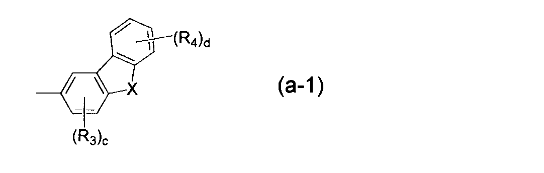
4.前記Qが下記式(a-2)で表される上記1又は2に記載の芳香族アミン誘導体、

5.前記L1及びL2の少なくとも一方が、単結合又は下記式(b-1)~(b-3)のいずれかで表される連結基である上記1~4のいずれかに記載の芳香族アミン誘導体、

R11~R13は、それぞれ独立に、フッ素原子、シアノ基、置換もしくは無置換の炭素数1~20のアルキル基、置換もしくは無置換の炭素数3~20のシクロアルキル基、置換もしくは無置換の炭素数1~20のアルコキシ基、置換もしくは無置換の炭素数1~20のハロアルキル基、置換もしくは無置換の炭素数1~20のハロアルコキシ基、置換もしくは無置換の炭素数1~10のアルキルシリル基、置換もしくは無置換の炭素数6~30のアリールシリル基、置換もしくは無置換の炭素数7~30のアラルキル基、置換もしくは無置換の環形成炭素数6~30のアリール基、又は、置換もしくは無置換の環形成炭素数5~30のヘテロアリール基であり、隣接するR11同士、隣接するR12同士、隣接するR13同士のそれぞれが互いに結合し、ベンゼン環の環形成炭素と共に環構造を形成してもよい。
R14、R15は、それぞれ独立に、水素原子、置換もしくは無置換の炭素数1~20のアルキル基、置換もしくは無置換の炭素数3~20のシクロアルキル基、置換もしくは無置換の炭素数1~20のハロアルキル基、置換もしくは無置換の炭素数7~30のアラルキル基、置換もしくは無置換の環形成炭素数6~30のアリール基、又は、置換もしくは無置換の環形成炭素数5~30のヘテロアリール基である。
k1~k3は、0~4の整数を表す。]
6.前記L1が前記式(b-1)~(b-3)のいずれかで表される連結基である上記5に記載の芳香族アミン誘導体、
7.前記L2が単結合又は前記式(b-1)~(b-3)のいずれかで表される連結基である上記5に記載の芳香族アミン誘導体、
8.前記L2が単結合又は前記式(b-1)で表される連結基である上記7に記載の芳香族アミン誘導体、
9.前記Xが酸素原子を表す上記1~8のいずれかに記載の芳香族アミン誘導体、
10.前記Xが硫黄原子を表す上記1~8のいずれかに記載の芳香族アミン誘導体、
11.上記1~10のいずれかに記載の芳香族アミン誘導体からなる有機エレクトロルミネッセンス素子用材料、
12.正孔輸送材料である上記11に記載の有機エレクトロルミネッセンス素子用材料、
13.陽極、陰極、及び該陽極と陰極の間に1層以上からなる有機薄膜層を有し、該有機薄膜層が発光層を含む有機エレクトロルミネッセンス素子であって、該有機薄膜層の少なくとも1層が上記1~10のいずれかに記載の芳香族アミン誘導体を含有することを特徴とする有機エレクトロルミネッセンス素子、
14.前記有機薄膜層が正孔輸送層を有し、前記芳香族アミン誘導体が該正孔輸送層に含有されている上記13に記載の有機エレクトロルミネッセンス素子、
15.前記正孔輸送層にアクセプター材料を含有する層が接合されている上記14に記載の有機エレクトロルミネッセンス素子、
16.前記アクセプター材料が、下記式(10)で表される上記15に記載の有機エレクトロルミネッセンス素子、

17.前記発光層が燐光発光材料を含有する上記13~16のいずれかに記載の有機エレクトロルミネッセンス素子、及び
18.前記燐光発光材料がイリジウム(Ir),オスミウム(Os)又は白金(Pt)金属のオルトメタル化錯体である上記17に記載の有機エレクトロルミネッセンス素子、
を提供するものである。 That is, the present invention
1. An aromatic amine derivative represented by the following formula (1):
L 1 represents a single bond, a substituted or unsubstituted arylene group having 6 to 30 ring carbon atoms, or a substituted or unsubstituted heteroarylene group having 5 to 30 ring carbon atoms.
L2 represents a single bond, a substituted or unsubstituted heteroarylene group having 5 to 30 ring carbon atoms, or a substituted or unsubstituted arylene group, and the arylene group includes a phenylene group, a biphenylylene group, a terphenylylene group, a naphthylene. Group, phenanthrylene group, chrysenylene group, peryleneylene group, and fluorenylene group.
Ar 1 and Ar 2 each independently represents a substituted or unsubstituted aryl group having 6 to 30 ring carbon atoms or a substituted or unsubstituted heteroaryl group having 5 to 30 ring carbon atoms.
R 1 and R 2 are each independently a fluorine atom, a cyano group, a substituted or unsubstituted alkyl group having 1 to 20 carbon atoms, a substituted or unsubstituted cycloalkyl group having 3 to 20 carbon atoms, substituted or unsubstituted An alkoxy group having 1 to 20 carbon atoms, a substituted or unsubstituted haloalkyl group having 1 to 20 carbon atoms, a substituted or unsubstituted haloalkoxy group having 1 to 20 carbon atoms, a substituted or unsubstituted 1 to 10 carbon atoms An alkylsilyl group, a substituted or unsubstituted arylsilyl group having 6 to 30 carbon atoms, a substituted or unsubstituted aralkyl group having 7 to 30 carbon atoms, a substituted or unsubstituted aryl group having 6 to 30 ring carbon atoms, or a substituted or unsubstituted ring forming a heteroaryl group having 5 to 30 carbon atoms, each other R 1 adjacent to each respective adjacent R 2 bonded to each other to each other, of the benzene rings Ring structure with formed carbon may be formed.
a represents an integer of 0 to 3.
b represents an integer of 0 to 4.
Q is a group represented by the following formula (a). ]
X represents an oxygen atom or a sulfur atom.
R 3 and R 4 are each independently a fluorine atom, a cyano group, a substituted or unsubstituted alkyl group having 1 to 20 carbon atoms, a substituted or unsubstituted cycloalkyl group having 3 to 20 carbon atoms, substituted or unsubstituted An alkoxy group having 1 to 20 carbon atoms, a substituted or unsubstituted haloalkyl group having 1 to 20 carbon atoms, a substituted or unsubstituted haloalkoxy group having 1 to 20 carbon atoms, a substituted or unsubstituted 1 to 10 carbon atoms An alkylsilyl group, a substituted or unsubstituted arylsilyl group having 6 to 30 carbon atoms, a substituted or unsubstituted aralkyl group having 7 to 30 carbon atoms, a substituted or unsubstituted aryl group having 6 to 30 ring carbon atoms, or a substituted or unsubstituted ring forming a heteroaryl group having 5 to 30 carbon atoms, the adjacent R 3 together, respectively between R 4 adjacent to bind to each other, of the benzene rings Ring structure with formed carbon may be formed.
c represents an integer of 0 to 3.
d represents an integer of 0 to 4. ]
2. The aromatic amine derivative according to the above 1, represented by the following formula (1-1):
3. The aromatic amine derivative according to 1 or 2, wherein Q is represented by the following formula (a-1):
4). The aromatic amine derivative according to 1 or 2, wherein Q is represented by the following formula (a-2):
5. The aromatic according to any one of 1 to 4 above, wherein at least one of L 1 and L 2 is a single bond or a linking group represented by any one of the following formulas (b-1) to (b-3): Amine derivatives,
R 11 to R 13 are each independently a fluorine atom, a cyano group, a substituted or unsubstituted alkyl group having 1 to 20 carbon atoms, a substituted or unsubstituted cycloalkyl group having 3 to 20 carbon atoms, substituted or unsubstituted An alkoxy group having 1 to 20 carbon atoms, a substituted or unsubstituted haloalkyl group having 1 to 20 carbon atoms, a substituted or unsubstituted haloalkoxy group having 1 to 20 carbon atoms, a substituted or unsubstituted 1 to 10 carbon atoms An alkylsilyl group, a substituted or unsubstituted arylsilyl group having 6 to 30 carbon atoms, a substituted or unsubstituted aralkyl group having 7 to 30 carbon atoms, a substituted or unsubstituted aryl group having 6 to 30 ring carbon atoms, or Substituted or unsubstituted heteroaryl groups having 5 to 30 ring carbon atoms, each of adjacent R 11 , adjacent R 12 , and adjacent R 13 are bonded to each other. And may form a ring structure together with the ring-forming carbon of the benzene ring.
R 14 and R 15 are each independently a hydrogen atom, a substituted or unsubstituted alkyl group having 1 to 20 carbon atoms, a substituted or unsubstituted cycloalkyl group having 3 to 20 carbon atoms, a substituted or unsubstituted carbon number. A haloalkyl group having 1 to 20 carbon atoms, a substituted or unsubstituted aralkyl group having 7 to 30 carbon atoms, a substituted or unsubstituted aryl group having 6 to 30 ring carbon atoms, or a substituted or unsubstituted ring carbon number having 5 to 5 carbon atoms; 30 heteroaryl groups.
k 1 to k 3 represent integers of 0 to 4. ]
6). 6. The aromatic amine derivative according to 5 above, wherein L 1 is a linking group represented by any one of formulas (b-1) to (b-3),
7). 6. The aromatic amine derivative according to 5 above, wherein L 2 is a single bond or a linking group represented by any one of formulas (b-1) to (b-3),
8). The aromatic amine derivative according to the above 7, wherein L 2 is a single bond or a linking group represented by the formula (b-1),
9. The aromatic amine derivative according to any one of 1 to 8 above, wherein X represents an oxygen atom,
10. The aromatic amine derivative according to any one of 1 to 8 above, wherein X represents a sulfur atom,
11. A material for an organic electroluminescence device comprising the aromatic amine derivative according to any one of 1 to 10 above,
12 The material for an organic electroluminescence device according to the above 11, which is a hole transport material,
13. An organic electroluminescence device comprising an anode, a cathode, and an organic thin film layer comprising one or more layers between the anode and the cathode, wherein the organic thin film layer includes a light emitting layer, wherein at least one of the organic thin film layers is An organic electroluminescence device comprising the aromatic amine derivative according to any one of 1 to 10 above,
14 14. The organic electroluminescence device according to 13, wherein the organic thin film layer has a hole transport layer, and the aromatic amine derivative is contained in the hole transport layer.
15. 15. The organic electroluminescence device according to 14 above, wherein a layer containing an acceptor material is bonded to the hole transport layer,
16. The organic electroluminescence device according to 15 above, wherein the acceptor material is represented by the following formula (10):
17. 17. The organic electroluminescent device according to any one of the above 13 to 16, wherein the light emitting layer contains a phosphorescent material, and 18. The organic electroluminescence device according to 17 above, wherein the phosphorescent material is an orthometalated complex of iridium (Ir), osmium (Os) or platinum (Pt) metal,
Is to provide.
本発明の芳香族アミン誘導体は、下記式(1)で表される。


R11~R13は、それぞれ独立に、フッ素原子、シアノ基、置換もしくは無置換の炭素数1~20、好ましくは1~10、より好ましくは1~5のアルキル基、置換もしくは無置換の炭素数3~20、好ましくは3~10、より好ましくは3~6のシクロアルキル基、置換もしくは無置換の炭素数1~20、好ましくは1~10、より好ましくは1~5のアルコキシ基、置換もしくは無置換の炭素数1~20、好ましくは1~10、より好ましくは1~5のハロアルキル基、置換もしくは無置換の炭素数1~20、好ましくは1~10、より好ましくは1~5のハロアルコキシ基、置換もしくは無置換の炭素数1~10、好ましくは1~5、より好ましくは1~3のアルキルシリル基、置換もしくは無置換の炭素数6~30、好ましくは6~24、より好ましくは6~18のアリールシリル基、置換もしくは無置換の炭素数7~30、好ましくは7~25、より好ましくは7~13のアラルキル基、置換もしくは無置換の環形成炭素数6~30、好ましくは6~24、より好ましくは6~12のアリール基、又は、置換もしくは無置換の環形成炭素数5~30、好ましくは5~24、より好ましくは5~12のヘテロアリール基であり、隣接するR11同士、隣接するR12同士、隣接するR13同士のそれぞれは互いに結合し、ベンゼン環の環形成炭素と共に環構造を形成してもよい。 In the formulas (b-1) to (b-3),
R 11 to R 13 are each independently a fluorine atom, a cyano group, a substituted or unsubstituted alkyl group having 1 to 20, preferably 1 to 10, more preferably 1 to 5 carbon atoms, a substituted or unsubstituted carbon. A cycloalkyl group having 3 to 20, preferably 3 to 10, more preferably 3 to 6, a substituted or unsubstituted C 1-20, preferably 1 to 10, more preferably 1 to 5 alkoxy group, substituted Or an unsubstituted haloalkyl group having 1 to 20, preferably 1 to 10, more preferably 1 to 5 carbon atoms, a substituted or unsubstituted carbon atom having 1 to 20, preferably 1 to 10, more preferably 1 to 5 carbon atoms. A haloalkoxy group, a substituted or unsubstituted alkylsilyl group having 1 to 10 carbon atoms, preferably 1 to 5 carbon atoms, more preferably 1 to 3 carbon atoms, a substituted or unsubstituted carbon atom number 6 to 30 carbon atoms, preferably 6 to 2 carbon atoms; 4, more preferably an arylsilyl group having 6 to 18 carbon atoms, a substituted or unsubstituted carbon number of 7 to 30, preferably 7 to 25, more preferably 7 to 13 carbon atoms, a substituted or unsubstituted ring carbon number of 6 -30, preferably 6-24, more preferably 6-12 aryl group, or a substituted or unsubstituted heteroaryl group having 5-30, preferably 5-24, more preferably 5-12 ring-forming carbon atoms. Each of adjacent R 11 , adjacent R 12 , and adjacent R 13 may be bonded to each other to form a ring structure together with the ring-forming carbon of the benzene ring.


次に、本発明の有機EL素子について説明する。
本発明の有機EL素子は、陰極と陽極の間に1層以上からなる有機薄膜層を有する。該有機薄膜層は発光層を有し、該有機薄膜層のうちの少なくとも1層が前述した本発明の芳香族アミン誘導体を含むことを特徴とする。本発明の芳香族アミン誘導体が、本発明の有機EL素子の有機薄膜層のうちの少なくとも一層に含有されることで、有機EL素子の高発光効率化、長寿命化が期待できる。
本発明の芳香族アミン誘導体が含まれる有機薄膜層の例としては、正孔輸送層、発光層、スペース層、及び障壁層等が挙げられるが、これらに限定されるものではない。本発明の芳香族アミン誘導体は、特に、正孔輸送層に含まれることが好ましい。また、発光層は蛍光発光材料や燐光発光材料を含有することが好ましく、特に燐光発光材料を含有することが好ましい。 Organic EL Element Next, the organic EL element of the present invention will be described.
The organic EL device of the present invention has an organic thin film layer composed of one or more layers between a cathode and an anode. The organic thin film layer includes a light emitting layer, and at least one of the organic thin film layers includes the above-described aromatic amine derivative of the present invention. When the aromatic amine derivative of the present invention is contained in at least one of the organic thin film layers of the organic EL element of the present invention, it can be expected that the organic EL element has high luminous efficiency and long life.
Examples of the organic thin film layer containing the aromatic amine derivative of the present invention include, but are not limited to, a hole transport layer, a light emitting layer, a space layer, and a barrier layer. The aromatic amine derivative of the present invention is particularly preferably contained in the hole transport layer. Further, the light emitting layer preferably contains a fluorescent light emitting material or a phosphorescent light emitting material, and particularly preferably contains a phosphorescent light emitting material.
(1)陽極/発光ユニット/陰極
また、上記発光ユニットは、燐光発光層や蛍光発光層を複数有する積層型であってもよく、その場合、各発光層の間に、燐光発光層で生成された励起子が蛍光発光層に拡散することを防ぐ目的で、スペース層を有していてもよい。発光ユニットの代表的な層構成を以下に示す。
(a)正孔輸送層/発光層(/電子輸送層)
(b)正孔輸送層/第一燐光発光層/第二燐光発光層(/電子輸送層)
(c)正孔輸送層/燐光発光層/スペース層/蛍光発光層(/電子輸送層)
(d)正孔輸送層/第一燐光発光層/第二燐光発光層/スペース層/蛍光発光層(/電子輸送層)
(e)正孔輸送層/第一燐光発光層/スペース層/第二燐光発光層/スペース層/蛍光発光層(/電子輸送層)
(f)正孔輸送層/燐光発光層/スペース層/第一蛍光発光層/第二蛍光発光層(/電子輸送層) Accordingly, typical element configurations of simple organic EL elements include the following element configurations.
(1) Anode / light emitting unit / cathode The above light emitting unit may be a laminated type having a plurality of phosphorescent light emitting layers and fluorescent light emitting layers. In that case, the light emitting unit is generated by a phosphorescent light emitting layer between the light emitting layers. In order to prevent the excitons from diffusing into the fluorescent light emitting layer, a space layer may be provided. A typical layer structure of the light emitting unit is shown below.
(A) Hole transport layer / light emitting layer (/ electron transport layer)
(B) Hole transport layer / first phosphorescent light emitting layer / second phosphorescent light emitting layer (/ electron transport layer)
(C) Hole transport layer / phosphorescent layer / space layer / fluorescent layer (/ electron transport layer)
(D) Hole transport layer / first phosphorescent light emitting layer / second phosphorescent light emitting layer / space layer / fluorescent light emitting layer (/ electron transport layer)
(E) Hole transport layer / first phosphorescent light emitting layer / space layer / second phosphorescent light emitting layer / space layer / fluorescent light emitting layer (/ electron transport layer)
(F) Hole transport layer / phosphorescent layer / space layer / first fluorescent layer / second fluorescent layer (/ electron transport layer)
なお、各発光層と正孔輸送層あるいはスペース層との間には、適宜、電子障壁層を設けてもよい。また、各発光層と電子輸送層との間には、適宜、正孔障壁層を設けてもよい。電子障壁層や正孔障壁層を設けることで、電子又は正孔を発光層内に閉じ込めて、発光層における電荷の再結合確率を高め、発光効率を向上させることができる。 Each phosphorescent or fluorescent light-emitting layer may have a different emission color. Specifically, in the laminated light emitting layer (d), hole transport layer / first phosphorescent light emitting layer (red light emitting) / second phosphorescent light emitting layer (green light emitting) / space layer / fluorescent light emitting layer (blue light emitting) / A layer structure such as an electron transport layer can be used.
An electron barrier layer may be appropriately provided between each light emitting layer and the hole transport layer or space layer. Further, a hole blocking layer may be appropriately provided between each light emitting layer and the electron transport layer. By providing an electron barrier layer or a hole barrier layer, electrons or holes can be confined in the light emitting layer, the recombination probability of charges in the light emitting layer can be increased, and the light emission efficiency can be improved.
(2)陽極/第一発光ユニット/中間層/第二発光ユニット/陰極
ここで、上記第一発光ユニット及び第二発光ユニットとしては、例えば、それぞれ独立に上述の発光ユニットと同様のものを選択することができる。
上記中間層は、一般的に、中間電極、中間導電層、電荷発生層、電子引抜層、接続層、中間絶縁層とも呼ばれ、第一発光ユニットに電子を、第二発光ユニットに正孔を供給する、公知の材料構成を用いることができる。 The following element structure can be mentioned as a typical element structure of a tandem type organic EL element.
(2) Anode / first light emitting unit / intermediate layer / second light emitting unit / cathode Here, as the first light emitting unit and the second light emitting unit, for example, the same light emitting unit as that described above is selected independently. can do.
The intermediate layer is generally called an intermediate electrode, an intermediate conductive layer, a charge generation layer, an electron extraction layer, a connection layer, or an intermediate insulating layer, and has electrons in the first light emitting unit and holes in the second light emitting unit. A known material structure to be supplied can be used.
本発明の有機EL素子は、透光性基板上に作製する。透光性基板は有機EL素子を支持する基板であり、400nm~700nmの可視領域の光の透過率が50%以上で平滑な基板が好ましい。具体的には、ガラス板、ポリマー板等が挙げられる。ガラス板としては、特にソーダ石灰ガラス、バリウム/ストロンチウム含有ガラス、鉛ガラス、アルミノケイ酸ガラス、ホウケイ酸ガラス、バリウムホウケイ酸ガラス、石英等を原料として用いてなるものを挙げられる。またポリマー板としては、ポリカーボネート、アクリル、ポリエチレンテレフタレート、ポリエーテルサルファイド、ポリサルフォン等を原料として用いてなるものを挙げることができる。 Substrate The organic EL device of the present invention is produced on a light-transmitting substrate. The light-transmitting substrate is a substrate that supports the organic EL element, and is preferably a smooth substrate having a light transmittance in the visible region of 400 nm to 700 nm of 50% or more. Specifically, a glass plate, a polymer plate, etc. are mentioned. Examples of the glass plate include those using soda lime glass, barium / strontium-containing glass, lead glass, aluminosilicate glass, borosilicate glass, barium borosilicate glass, quartz and the like as raw materials. Examples of the polymer plate include those using polycarbonate, acrylic, polyethylene terephthalate, polyether sulfide, polysulfone and the like as raw materials.
有機EL素子の陽極は、正孔を正孔輸送層又は発光層に注入する役割を担うものであり、4.5eV以上の仕事関数を有するものを用いることが効果的である。陽極材料の具体例としては、酸化インジウム錫合金(ITO)、酸化錫(NESA)、酸化インジウム亜鉛酸化物、金、銀、白金、銅等が挙げられる。陽極はこれらの電極物質を蒸着法やスパッタリング法等の方法で薄膜を形成させることにより作製することができる。発光層からの発光を陽極から取り出す場合、陽極の可視領域の光の透過率を10%より大きくすることが好ましい。また、陽極のシート抵抗は、数百Ω/□以下が好ましい。陽極の膜厚は、材料にもよるが、通常10nm~1μm、好ましくは10nm~200nmの範囲で選択される。 Anode The anode of the organic EL element plays a role of injecting holes into the hole transport layer or the light emitting layer, and it is effective to use one having a work function of 4.5 eV or more. Specific examples of the anode material include indium tin oxide alloy (ITO), tin oxide (NESA), indium zinc oxide, gold, silver, platinum, copper, and the like. The anode can be produced by forming a thin film of these electrode materials by a method such as vapor deposition or sputtering. When light emitted from the light emitting layer is extracted from the anode, it is preferable that the transmittance of light in the visible region of the anode is greater than 10%. The sheet resistance of the anode is preferably several hundred Ω / □ or less. The film thickness of the anode depends on the material, but is usually selected in the range of 10 nm to 1 μm, preferably 10 nm to 200 nm.
陰極は電子注入層、電子輸送層又は発光層に電子を注入する役割を担うものであり、仕事関数の小さい材料により形成するのが好ましい。陰極材料は特に限定されないが、具体的にはインジウム、アルミニウム、マグネシウム、マグネシウム-インジウム合金、マグネシウム-アルミニウム合金、アルミニウム-リチウム合金、アルミニウム-スカンジウム-リチウム合金、マグネシウム-銀合金等が使用できる。陰極も、陽極と同様に、蒸着法やスパッタリング法等の方法で薄膜を形成させることにより作製することができる。また、必要に応じて、陰極側から発光を取り出してもよい。 Cathode The cathode plays a role of injecting electrons into the electron injection layer, the electron transport layer, or the light emitting layer, and is preferably formed of a material having a small work function. The cathode material is not particularly limited, and specifically, indium, aluminum, magnesium, magnesium-indium alloy, magnesium-aluminum alloy, aluminum-lithium alloy, aluminum-scandium-lithium alloy, magnesium-silver alloy and the like can be used. Similarly to the anode, the cathode can be produced by forming a thin film by a method such as vapor deposition or sputtering. Moreover, you may take out light emission from the cathode side as needed.
発光機能を有する有機層であって、ドーピングシステムを採用する場合、ホスト材料とドーパント材料を含んでいる。このとき、ホスト材料は、主に電子と正孔の再結合を促し、励起子を発光層内に閉じ込める機能を有し、ドーパント材料は、再結合で得られた励起子を効率的に発光させる機能を有する。
燐光素子の場合、ホスト材料は主にドーパントで生成された励起子を発光層内に閉じ込める機能を有する。 Light-emitting layer An organic layer having a light-emitting function, and when a doping system is employed, includes a host material and a dopant material. At this time, the host material mainly has a function of encouraging recombination of electrons and holes and confining excitons in the light emitting layer, and the dopant material efficiently emits excitons obtained by recombination. It has a function.
In the case of a phosphorescent element, the host material mainly has a function of confining excitons generated by the dopant in the light emitting layer.
また、量子収率の高いドーパント材料を二種類以上入れることによって、それぞれのドーパントが発光するダブルドーパントを採用してもよい。具体的には、ホスト、赤色ドーパント及び緑色ドーパントを共蒸着することによって、発光層を共通化して黄色発光を実現する態様が挙げられる。 Here, the light emitting layer employs, for example, a double host (also referred to as a host / cohost) that adjusts the carrier balance in the light emitting layer by combining an electron transporting host and a hole transporting host. Also good.
Moreover, you may employ | adopt the double dopant from which each dopant light-emits by putting in 2 or more types of dopant materials with a high quantum yield. Specifically, a mode in which yellow emission is realized by co-evaporating a host, a red dopant, and a green dopant to make the light emitting layer common is used.


本発明の芳香族アミン誘導体とそれ以外の化合物を同一の発光層内の燐光ホスト材料として併用してもよいし、複数の発光層がある場合には、そのうちの一つの発光層の燐光ホスト材料として本発明の芳香族アミン誘導体を用い、別の一つの発光層の燐光ホスト材料として本発明の芳香族アミン誘導体以外の化合物を用いてもよい。また、本発明の芳香族アミン誘導体は発光層以外の有機層にも使用しうるものであり、その場合には発光層の燐光ホストとして、本発明の芳香族アミン誘導体以外の化合物を用いてもよい。 The phosphorescent host is a compound having a function of efficiently emitting the phosphorescent dopant by efficiently confining the triplet energy of the phosphorescent dopant in the light emitting layer. Although the aromatic amine derivative of the present invention is useful as a phosphorescent host, compounds other than the aromatic amine derivative of the present invention can be appropriately selected as the phosphorescent host according to the above-mentioned purpose.
The aromatic amine derivative of the present invention and other compounds may be used in combination as a phosphorescent host material in the same light emitting layer, and when there are a plurality of light emitting layers, the phosphorescent host material of one of the light emitting layers The aromatic amine derivative of the present invention may be used, and a compound other than the aromatic amine derivative of the present invention may be used as the phosphorescent host material of another light emitting layer. In addition, the aromatic amine derivative of the present invention can be used in an organic layer other than the light emitting layer. In that case, a compound other than the aromatic amine derivative of the present invention may be used as the phosphorescent host of the light emitting layer. Good.

本発明の有機EL素子は、陰極と発光ユニットとの界面領域に電子供与性ドーパントを有することも好ましい。このような構成によれば、有機EL素子における発光輝度の向上や長寿命化が図られる。ここで、電子供与性ドーパントとは、仕事関数3.8eV以下の金属を含有するものをいい、その具体例としては、アルカリ金属、アルカリ金属錯体、アルカリ金属化合物、アルカリ土類金属、アルカリ土類金属錯体、アルカリ土類金属化合物、希土類金属、希土類金属錯体、及び希土類金属化合物等から選ばれた少なくとも一種類が挙げられる。 Electron-donating dopant The organic EL device of the present invention preferably has an electron-donating dopant in the interface region between the cathode and the light emitting unit. According to such a configuration, it is possible to improve the light emission luminance and extend the life of the organic EL element. Here, the electron donating dopant means a material containing a metal having a work function of 3.8 eV or less, and specific examples thereof include alkali metals, alkali metal complexes, alkali metal compounds, alkaline earth metals, alkaline earths. Examples thereof include at least one selected from metal complexes, alkaline earth metal compounds, rare earth metals, rare earth metal complexes, rare earth metal compounds, and the like.
本発明の有機EL素子における、主成分と電子供与性ドーパントの割合は、モル比で主成分:電子供与性ドーパント=5:1~1:5であると好ましく、2:1~1:2であるとさらに好ましい。 In the case where the electron donating dopant is formed in a layered form, after forming the light emitting material or the electron injecting material, which is an organic layer at the interface, in a layered form, the reducing dopant is vapor-deposited by a resistance heating vapor deposition method. .1 nm to 15 nm. When the electron donating dopant is formed in an island shape, after forming the light emitting material and the electron injecting material, which are organic layers at the interface, in an island shape, the electron donating dopant is deposited by resistance heating vapor deposition alone, preferably The island is formed with a thickness of 0.05 nm to 1 nm.
In the organic EL device of the present invention, the ratio of the main component to the electron donating dopant is preferably the main component: electron donating dopant = 5: 1 to 1: 5 in a molar ratio of 2: 1 to 1: 2. More preferably.
発光層と陰極との間に形成される有機層であって、電子を陰極から発光層へ輸送する機能を有する。電子輸送層が複数層で構成される場合、陰極に近い有機層を電子注入層と定義することがある。電子注入層は、陰極から電子を効率的に有機層ユニットに注入する機能を有する。 Electron transport layer An organic layer formed between the light emitting layer and the cathode, and has a function of transporting electrons from the cathode to the light emitting layer. When the electron transport layer is composed of a plurality of layers, an organic layer close to the cathode may be defined as an electron injection layer. The electron injection layer has a function of efficiently injecting electrons from the cathode into the organic layer unit.
この含窒素環誘導体としては、例えば、下記式(A)で表される含窒素環金属キレート錯体が好ましい。 As the electron transporting material used for the electron transporting layer, an aromatic heterocyclic compound containing one or more heteroatoms in the molecule is preferably used, and a nitrogen-containing ring derivative is particularly preferable. The nitrogen-containing ring derivative is preferably an aromatic ring having a nitrogen-containing 6-membered ring or 5-membered ring skeleton, or a condensed aromatic ring compound having a nitrogen-containing 6-membered ring or 5-membered ring skeleton.
As this nitrogen-containing ring derivative, for example, a nitrogen-containing ring metal chelate complex represented by the following formula (A) is preferable.

アルキルアミノ基及びアラルキルアミノ基は-NQ1Q2と表される。Q1及びQ2は、それぞれ独立に、炭素数1~20のアルキル基又は炭素数7~30のアラルキル基を表す。Q1及びQ2の一方は水素原子又は重水素原子であってもよい。
アリールアミノ基は-NAr1Ar2と表され、Ar1及びAr2は、それぞれ独立に、環形成炭素数6~50の非縮合芳香族炭化水素基及び縮合芳香族炭化水素基を表す。Ar1及びAr2の一方は水素原子又は重水素原子であってもよい。 Examples of the substituted amino group include an alkylamino group, an arylamino group, and an aralkylamino group.
The alkylamino group and the aralkylamino group are represented as —NQ 1 Q 2 . Q 1 and Q 2 each independently represents an alkyl group having 1 to 20 carbon atoms or an aralkyl group having 7 to 30 carbon atoms. One of Q 1 and Q 2 may be a hydrogen atom or a deuterium atom.
The arylamino group is represented as —NAr 1 Ar 2, and Ar 1 and Ar 2 each independently represent a non-condensed aromatic hydrocarbon group and a condensed aromatic hydrocarbon group having 6 to 50 ring carbon atoms. One of Ar 1 and Ar 2 may be a hydrogen atom or a deuterium atom.


HAr-L1-Ar1-Ar2
前記式中、HArは、置換もしくは無置換の環形成炭素数3~40の含窒素複素環基であり、L1は単結合、置換もしくは無置換の環形成炭素数6~40の非縮合芳香族炭化水素基又は縮合芳香族炭化水素基又は置換もしくは無置換の環形成炭素数3~40の非縮合芳香族複素環基又は縮合芳香族複素環基であり、Ar1は置換もしくは無置換の環形成炭素数6~40の2価の芳香族炭化水素基であり、Ar2は置換もしくは無置換の環形成炭素数6~40の非縮合芳香族炭化水素基又は縮合芳香族炭化水素基又は置換もしくは無置換の環形成炭素数3~40の非縮合芳香族複素環基又は縮合芳香族複素環基である。 Furthermore, preferred specific compounds include nitrogen-containing heterocyclic derivatives represented by the following formula.
HAr-L 1 -Ar 1 -Ar 2
In the above formula, HAr is a substituted or unsubstituted nitrogen-containing heterocyclic group having 3 to 40 ring carbon atoms, and L 1 is a single bond, a substituted or unsubstituted non-condensed aromatic group having 6 to 40 ring carbon atoms. An aromatic hydrocarbon group, a condensed aromatic hydrocarbon group, a substituted or unsubstituted non-condensed aromatic heterocyclic group having 3 to 40 carbon atoms or a condensed aromatic heterocyclic group, and Ar 1 is a substituted or unsubstituted aromatic group. A divalent aromatic hydrocarbon group having 6 to 40 ring carbon atoms, and Ar 2 is a substituted or unsubstituted non-condensed aromatic hydrocarbon group or condensed aromatic hydrocarbon group having 6 to 40 ring carbon atoms, or A substituted or unsubstituted ring-unformed aromatic heterocyclic group having 3 to 40 carbon atoms or a condensed aromatic heterocyclic group;


R1及びR2は、それぞれ独立に、置換もしくは無置換の環形成炭素数6~50のアリール基、置換もしくは無置換の環形成原子数5~50のヘテロアリール基、置換もしくは無置換の炭素数1~20のアルキル基、置換もしくは無置換の炭素数1~20のハロアルキル基又は置換もしくは無置換の炭素数1~20のアルコキシ基である。
nは、0~5の整数であり、nが2以上の整数であるとき、複数のR1は互いに同一でも異なっていてもよい。また、隣接する2つのR1同士が互いに結合して、置換もしくは無置換の炭化水素環を形成していてもよい。
Ar1は、置換もしくは無置換の環形成炭素数6~50のアリール基又は置換もしくは無置換の環形成原子数5~50のヘテロアリール基である。
Ar2は、水素原子、置換もしくは無置換の炭素数1~20のアルキル基、置換もしくは無置換の炭素数1~20のハロアルキル基、置換もしくは無置換の炭素数1~20のアルコキシ基、置換もしくは無置換の環形成炭素数6~50のアリール基又は置換もしくは無置換の環形成原子数5~50のヘテロアリール基である。
但し、Ar1、Ar2のいずれか一方は、置換もしくは無置換の環形成炭素数10~50の縮合芳香族炭化水素環基又は置換もしくは無置換の環形成原子数9~50の縮合芳香族複素環基である。
Ar3は、置換もしくは無置換の環形成炭素数6~50のアリーレン基又は置換もしくは無置換の環形成原子数5~50のヘテロアリーレン基である。
L1、L2及びL3は、それぞれ独立に、単結合、置換もしくは無置換の環形成炭素数6~50のアリーレン基、又は置換もしくは無置換の環形成原子数9~50の2価の縮合芳香族複素環基である。) (In the formula, Z 1 , Z 2 and Z 3 are each independently a nitrogen atom or a carbon atom.
R 1 and R 2 are each independently a substituted or unsubstituted aryl group having 6 to 50 ring carbon atoms, a substituted or unsubstituted heteroaryl group having 5 to 50 ring atoms, substituted or unsubstituted carbon An alkyl group having 1 to 20 carbon atoms, a substituted or unsubstituted haloalkyl group having 1 to 20 carbon atoms, or a substituted or unsubstituted alkoxy group having 1 to 20 carbon atoms.
n is an integer of 0 to 5, and when n is an integer of 2 or more, the plurality of R 1 may be the same or different from each other. Further, two adjacent R 1 's may be bonded to each other to form a substituted or unsubstituted hydrocarbon ring.
Ar 1 is a substituted or unsubstituted aryl group having 6 to 50 ring carbon atoms or a substituted or unsubstituted heteroaryl group having 5 to 50 ring atoms.
Ar 2 is a hydrogen atom, a substituted or unsubstituted alkyl group having 1 to 20 carbon atoms, a substituted or unsubstituted haloalkyl group having 1 to 20 carbon atoms, a substituted or unsubstituted alkoxy group having 1 to 20 carbon atoms, substituted Alternatively, it is an unsubstituted aryl group having 6 to 50 ring carbon atoms or a substituted or unsubstituted heteroaryl group having 5 to 50 ring atoms.
However, either Ar 1 or Ar 2 is a substituted or unsubstituted condensed aromatic hydrocarbon ring group having 10 to 50 ring carbon atoms or a substituted or unsubstituted condensed aromatic group having 9 to 50 ring atoms. It is a heterocyclic group.
Ar 3 is a substituted or unsubstituted arylene group having 6 to 50 ring carbon atoms or a substituted or unsubstituted heteroarylene group having 5 to 50 ring atoms.
L 1 , L 2 and L 3 are each independently a single bond, a substituted or unsubstituted arylene group having 6 to 50 ring carbon atoms, or a divalent or substituted or unsubstituted divalent atom having 9 to 50 ring atoms. A condensed aromatic heterocyclic group. )
環形成原子数5~50のヘテロアリール基としては、ピローリル基、フリル基、チエニル基、シローリル基、ピリジル基、キノリル基、イソキノリル基、べンゾフリル基、イミダゾリル基、ピリミジル基、カルバゾリル基、セレノフェニル基、オキサジアゾリル基、トリアゾーリル基、ピラジニル基、ピリダジニル基、トリアジニル基、キノキサリニル基、アクリジニル基、イミダゾ[1,2-a]ピリジニル基、イミダゾ[1,2-a]ピリミジニル基などが挙げられる。
炭素数1~20のアルキル基としては、メチル基、エチル基、プロピル基、ブチル基、ペンチル基、へキシル基などが挙げられる。
炭素数1~20のハロアルキル基としては、前記アルキル基の1又は2以上の水素原子をフッ素、塩素、ヨウ素および臭素から選ばれる少なくとも1のハロゲン原子で置換して得られる基が挙げられる。
炭素数1~20のアルコキシ基としては、前記アルキル基をアルキル部位として有する基が挙げられる。
環形成炭素数6~50のアリーレン基としては、前記アリール基から水素原子1個を除去して得られる基が挙げられる。
環形成原子数9~50の2価の縮合芳香族複素環基としては、前記ヘテロアリール基から水素原子1個を除去して得られる基が挙げられる。 Examples of the aryl group having 6 to 50 ring carbon atoms include phenyl group, naphthyl group, anthryl group, phenanthryl group, naphthacenyl group, chrysenyl group, pyrenyl group, biphenyl group, terphenyl group, tolyl group, fluoranthenyl group, fluorenyl Groups and the like.
Examples of heteroaryl groups having 5 to 50 ring atoms include pyrrolyl, furyl, thienyl, silolyl, pyridyl, quinolyl, isoquinolyl, benzofuryl, imidazolyl, pyrimidyl, carbazolyl, selenophenyl Group, oxadiazolyl group, triazolyl group, pyrazinyl group, pyridazinyl group, triazinyl group, quinoxalinyl group, acridinyl group, imidazo [1,2-a] pyridinyl group, imidazo [1,2-a] pyrimidinyl group and the like.
Examples of the alkyl group having 1 to 20 carbon atoms include a methyl group, an ethyl group, a propyl group, a butyl group, a pentyl group, and a hexyl group.
Examples of the haloalkyl group having 1 to 20 carbon atoms include groups obtained by substituting one or more hydrogen atoms of the alkyl group with at least one halogen atom selected from fluorine, chlorine, iodine and bromine.
Examples of the alkoxy group having 1 to 20 carbon atoms include groups having the alkyl group as an alkyl moiety.
Examples of the arylene group having 6 to 50 ring carbon atoms include groups obtained by removing one hydrogen atom from the aryl group.
Examples of the divalent condensed aromatic heterocyclic group having 9 to 50 ring atoms include groups obtained by removing one hydrogen atom from the heteroaryl group.
正孔輸送層は発光層と陽極との間に形成される有機層であって、正孔を陽極から発光層へ輸送する機能を有する。正孔輸送層が複数層で構成される場合、陽極に近い有機層を正孔注入層と定義することがある。正孔注入層は、陽極から正孔を効率的に有機層ユニットに注入する機能を有する。 Hole transport layer The hole transport layer is an organic layer formed between the light emitting layer and the anode, and has a function of transporting holes from the anode to the light emitting layer. When the hole transport layer is composed of a plurality of layers, an organic layer close to the anode may be defined as a hole injection layer. The hole injection layer has a function of efficiently injecting holes from the anode into the organic layer unit.

また、前記一般式(I)において、Lは置換もしくは無置換の環形成炭素数6~50の非縮合芳香族炭化水素基又は縮合芳香族炭化水素基、又は置換もしくは無置換の環形成原子数5~50の非縮合芳香族複素環基又は縮合芳香族複素環基を表す。 In the above general formula (I), Ar 1 to Ar 4 are substituted or unsubstituted ring-condensed aromatic hydrocarbon groups or condensed aromatic hydrocarbon groups having 6 to 50 carbon atoms, substituted or unsubstituted ring-forming atoms. A non-condensed aromatic heterocyclic group or a condensed aromatic heterocyclic group of 5 to 50, or a non-condensed aromatic hydrocarbon group or a condensed aromatic hydrocarbon group and a non-condensed aromatic heterocyclic group or a condensed aromatic hetero group A group to which a cyclic group is bonded is represented.
In the general formula (I), L represents a substituted or unsubstituted non-condensed aromatic hydrocarbon group or condensed aromatic hydrocarbon group having 6 to 50 ring carbon atoms, or a substituted or unsubstituted ring forming atom number. It represents 5 to 50 non-condensed aromatic heterocyclic group or condensed aromatic heterocyclic group.


上述の正孔輸送層や電子輸送層においては、特許第3695714号明細書に記載されているように、ドナー性材料のドーピング(n)やアクセプター性材料のドーピング(p)により、キャリア注入能を調整することができる。
nドーピングの代表例としては、電子輸送材料にLiやCs等の金属をドーピングする方法が挙げられ、pドーピングの代表例としては、正孔輸送材料にF4TCNQ等のアクセプター材料をドーピングする方法が挙げられる。 n / p doping In the above-described hole transport layer and electron transport layer, as described in Japanese Patent No. 3695714, by doping (n) of donor material and doping (p) of acceptor material, The carrier injection ability can be adjusted.
A typical example of n doping is a method of doping an electron transport material with a metal such as Li or Cs. A typical example of p doping is a method of doping an acceptor material such as F 4 TCNQ into a hole transport material. Is mentioned.
上記スペース層とは、例えば、蛍光発光層と燐光発光層とを積層する場合に、燐光発光層で生成する励起子を蛍光発光層に拡散させない、あるいは、キャリアバランスを調整する目的で、蛍光発光層と燐光発光層との間に設けられる層である。また、スペース層は、複数の燐光発光層の間に設けることもできる。
スペース層は発光層間に設けられるため、電子輸送性と正孔輸送性を兼ね備える材料であることが好ましい。また、隣接する燐光発光層内の三重項エネルギーの拡散を防ぐため、三重項エネルギーが2.6eV以上であることが好ましい。スペース層に用いられる材料としては、上述の正孔輸送層に用いられるものと同様のものが挙げられる。 Space layer The space layer is, for example, in the case of laminating a fluorescent light emitting layer and a phosphorescent light emitting layer, for the purpose of adjusting the carrier balance so as not to diffuse excitons generated in the phosphorescent light emitting layer into the fluorescent light emitting layer. This is a layer provided between the fluorescent light emitting layer and the phosphorescent light emitting layer. In addition, the space layer can be provided between the plurality of phosphorescent light emitting layers.
Since the space layer is provided between the light emitting layers, a material having both electron transport properties and hole transport properties is preferable. In order to prevent diffusion of triplet energy in the adjacent phosphorescent light emitting layer, the triplet energy is preferably 2.6 eV or more. Examples of the material used for the space layer include the same materials as those used for the above-described hole transport layer.
本発明の有機EL素子は、発光層に隣接する部分に、電子障壁層、正孔障壁層、トリプレット障壁層といった障壁層を有することが好ましい。ここで、電子障壁層とは、発光層から正孔輸送層へ電子が漏れることを防ぐ層であり、正孔障壁層とは、発光層から電子輸送層へ正孔が漏れることを防ぐ層である。
トリプレット障壁層は、後述するように、発光層で生成する三重項励起子が、周辺の層へ拡散することを防止し、三重項励起子を発光層内に閉じ込めることによって三重項励起子の発光ドーパント以外の電子輸送層の分子上でのエネルギー失活を抑制する機能を有する。
トリプレット障壁層を設ける場合、発光層中の燐光発光性ドーパントの三重項エネルギーをET d、トリプレット障壁層として用いる化合物の三重項エネルギーをET TBとすると、ET d<ET TBのエネルギー大小関係であれば、エネルギー関係上、燐光発光性ドーパントの三重項励起子が閉じ込められ(他分子へ移動できなくなり)、該ドーパント上で発光する以外のエネルギー失活経路が断たれ、高効率に発光することができると推測される。ただし、ET d<ET TBの関係が成り立つ場合であってもこのエネルギー差ΔET=ET TB-ET dが小さい場合には、実際の素子駆動環境である室温程度の環境下では、周辺の熱エネルギーにより吸熱的にこのエネルギー差ΔETを乗り越えて三重項励起子が他分子へ移動することが可能であると考えられる。特に燐光発光の場合は蛍光発光に比べて励起子寿命が長いため、相対的に吸熱的励起子移動過程の影響が現れやすくなる。室温の熱エネルギーに対してこのエネルギー差ΔETは大きい程好ましく、0.1eV以上であると
さらに好ましく、0.2eV以上であると特に好ましい。 Barrier Layer The organic EL device of the present invention preferably has a barrier layer such as an electron barrier layer, a hole barrier layer, or a triplet barrier layer in a portion adjacent to the light emitting layer. Here, the electron barrier layer is a layer that prevents electrons from leaking from the light emitting layer to the hole transport layer, and the hole barrier layer is a layer that prevents holes from leaking from the light emitting layer to the electron transport layer. is there.
As will be described later, the triplet barrier layer prevents the triplet excitons generated in the light emitting layer from diffusing into the surrounding layers, and confines the triplet excitons in the light emitting layer, thereby emitting the triplet excitons. It has a function of suppressing energy deactivation on the molecule of the electron transport layer other than the dopant.
When providing the triplet barrier layer, the triplet energy E T d of the phosphorescent dopant in the light emitting layer and the triplet energy of the compound used as a triplet barrier layer and E T TB, energy E T d <E T TB If the size relationship is large, the triplet exciton of the phosphorescent dopant is confined (cannot move to other molecules) in terms of energy, and the energy deactivation path other than light emission on the dopant is interrupted, resulting in high efficiency. It is estimated that light can be emitted. However, even if the relationship of E T d <E T TB is satisfied, if this energy difference ΔE T = E T TB −E T d is small, the actual device drive environment is at about room temperature. , endothermically triplet excitons overcame this energy difference Delta] E T by thermal energy near is considered to be possible to move to another molecule. In particular, in the case of phosphorescence emission, the exciton lifetime is longer than that of fluorescence emission, so that the influence of the endothermic exciton transfer process is likely to appear. The energy difference ΔE T is preferably as large as possible relative to the thermal energy at room temperature, more preferably 0.1 eV or more, and particularly preferably 0.2 eV or more.
まず、試料をEPA溶媒(ジエチルエーテル:イソペンタン:エタノール=5:5:2(容積比))に10μmol/Lで溶解させ、燐光測定用試料とする。この燐光測定用試料を石英セルに入れ、温度77Kで励起光を照射し、放射される燐光の燐光スペクトルを測定する。これを基に換算式ET(eV)=1239.85/λedgeによって求めた値と定義する。「λedge」とは、縦軸に燐光強度、横軸に波長をとって、燐光スペクトルを表したときに、燐光スペクトルの短波長側の立ち上がりに対して接線を引き、その接線と横軸の交点の波長値(単位:nm)を意味する。
発光層のホスト材料としては、Ab-Ah≦0.1eVとなるものが好ましい。ここで、Abは障壁層材料の電子親和力を表し、Ahは発光層ホスト材料の電子親和力を表す。
本発明における電子親和力Afとは、材料の分子に電子を一つ与えた時に放出または吸収されるエネルギーをいい、放出の場合は正、吸収の場合は負と定義する。電子親和力Afは、イオン化ポテンシャルIpと光学エネルギーギャップEg(S)とにより次のように規定する。
Af=Ip-Eg(S)
ここで、イオン化ポテンシャルIpは、各材料の化合物から電子を取り去ってイオン化するために要するエネルギーを意味し、本発明では大気中光電子分光装置(AC-3、理研計器株式会社製)で測定した正の符号を持つ値である。光学エネルギーギャップEg(S)は、伝導レベルと価電子レベルとの差をいい、本発明では各材料のジクロロメタン希薄溶液の紫外・可視光吸収スペクトルの長波長側接線とベースライン(吸収ゼロ)との交点の波長値をエネルギーに換算して求めた正の符号を持つ値である。
また、トリプレット障壁層を構成する材料の電子移動度は、電界強度0.04~0.5MV/cmの範囲において、10-6cm2/Vs以上であることが好ましい。有機材料の電子移動度の測定方法としては、Time of Flight法等幾つかの方法が知られているが、ここではインピーダンス分光法で決定される電子移動度をいう。
電子注入層は、電界強度0.04~0.5MV/cmの範囲において、10-6cm2/Vs以上であることが好ましい。これにより陰極からの電子輸送層への電子注入が促進され、ひいては隣接する障壁層、発光層への電子注入も促進し、より低電圧での駆動を可能にするためである。 The triplet energy in the present invention is measured as follows.
First, a sample is dissolved in EPA solvent (diethyl ether: isopentane: ethanol = 5: 5: 2 (volume ratio)) at 10 μmol / L to obtain a sample for phosphorescence measurement. This phosphorescence measurement sample is put in a quartz cell, irradiated with excitation light at a temperature of 77 K, and the phosphorescence spectrum of the emitted phosphorescence is measured. Based on this, it is defined as a value obtained by a conversion formula E T (eV) = 1239.85 / λ edge . “Λ edge ” means that when the phosphorescence spectrum is expressed by taking the phosphorescence intensity on the vertical axis and the wavelength on the horizontal axis, a tangent line is drawn with respect to the rising edge on the short wavelength side of the phosphorescence spectrum. It means the wavelength value (unit: nm) at the intersection.
The host material for the light emitting layer is preferably a material satisfying A b −A h ≦ 0.1 eV. Here, A b represents an electron affinity of the barrier layer material, A h represents an electron affinity of the light emitting layer host material.
The electron affinity Af in the present invention means energy released or absorbed when one electron is given to a molecule of a material, and is defined as positive in the case of emission and negative in the case of absorption. The electron affinity Af is defined by the ionization potential Ip and the optical energy gap Eg (S) as follows.
Af = Ip-Eg (S)
Here, the ionization potential Ip means the energy required to remove and ionize electrons from the compound of each material. In the present invention, the ionization potential Ip is a positive value measured with an atmospheric photoelectron spectrometer (AC-3, manufactured by Riken Keiki Co., Ltd.). It is a value with the sign of. The optical energy gap Eg (S) refers to the difference between the conduction level and the valence level. In the present invention, the long wavelength side tangent and the baseline (zero absorption) of the ultraviolet / visible light absorption spectrum of the dilute dichloromethane solution of each material This is a value having a positive sign obtained by converting the wavelength value of the intersection point into energy.
In addition, the electron mobility of the material constituting the triplet barrier layer is preferably 10 −6 cm 2 / Vs or more in the range of electric field strength of 0.04 to 0.5 MV / cm. As a method for measuring the electron mobility of an organic material, several methods such as the Time of Flight method are known. Here, the electron mobility is determined by impedance spectroscopy.
The electron injection layer is preferably 10 −6 cm 2 / Vs or more in the range of electric field strength of 0.04 to 0.5 MV / cm. This facilitates the injection of electrons from the cathode into the electron transport layer, and also promotes the injection of electrons into the adjacent barrier layer and the light emitting layer, thereby enabling driving at a lower voltage.
アルゴン雰囲気下、2-ブロモ-9,9-ジメチルフルオレン55g(201.3mmol)にヨウ素23g(90.6mmol)、過ヨウ素酸2水和物9.4g(41.2mmol)、水42ml、酢酸360ml、及び硫酸11mlを加え、65℃で30分撹拌した後、90℃で6時間撹拌した。
反応終了後に反応物を氷水に注入し、析出した結晶を濾取した。水で洗浄後、メタノールで洗浄することにより、61gの白色固体を得た。FD-MS(電界脱離質量分析)により、下記中間体1-1と同定した。(収率76%)

Under an argon atmosphere, 55 g (201.3 mmol) of 2-bromo-9,9-dimethylfluorene, 23 g (90.6 mmol) of iodine, 9.4 g (41.2 mmol) of periodic acid dihydrate, 42 ml of water, 360 ml of acetic acid And 11 ml of sulfuric acid were added and stirred at 65 ° C. for 30 minutes, and then stirred at 90 ° C. for 6 hours.
After completion of the reaction, the reaction product was poured into ice water, and the precipitated crystals were collected by filtration. By washing with water and then with methanol, 61 g of a white solid was obtained. The following intermediate 1-1 was identified by FD-MS (field desorption mass spectrometry). (Yield 76%)
中間体合成例1-1において、2-ブロモ-9,9-ジメチルフルオレンの代わりに4-ブロモビフェニルを46.9g用いた以外は同様に反応を行ったところ、50.6gの白色固体を得た。FD-MSの分析により、下記中間体1-2と同定した。(収率70%)
In the same manner as in Intermediate Synthesis Example 1-1, except that 46.9 g of 4-bromobiphenyl was used instead of 2-bromo-9,9-dimethylfluorene, a reaction was performed to obtain 50.6 g of a white solid. It was. The following intermediate 1-2 was identified by analysis of FD-MS. (Yield 70%)
アルゴン雰囲気下、ジベンゾフラン78.0g(0.46mol)に脱水テトラヒドロフラン600mlを加え、-30℃に冷却し、1.65M濃度のn-ブチルリチウムヘキサン溶液300ml(0.50mol)を滴下して、攪拌しながら1時間かけて室温まで昇温した。室温で5時間撹拌後、-60℃まで冷却し、1,2-ジブロモエタン60ml(0.70mol)を1時間かけて滴下した。
室温で15時間撹拌した後、氷水1000mlに注ぎ、ジクロロメタンにて抽出した。有機層を飽和食塩水で洗浄した後、MgSO4で乾燥し、濾過、濃縮した。濃縮残渣をシリカゲルクロマトグラフィーで精製し、テトラヒドロフラン/メタノールで洗浄し、70gの固体を得た。FD-MSの分析により、下記中間体1-3と同定した。(収率62%)

In an argon atmosphere, 600 ml of dehydrated tetrahydrofuran was added to 78.0 g (0.46 mol) of dibenzofuran, cooled to −30 ° C., and 300 ml (0.50 mol) of a 1.65M n-butyllithium hexane solution was added dropwise and stirred. The temperature was raised to room temperature over 1 hour. After stirring at room temperature for 5 hours, the mixture was cooled to −60 ° C., and 60 ml (0.70 mol) of 1,2-dibromoethane was added dropwise over 1 hour.
After stirring at room temperature for 15 hours, the mixture was poured into 1000 ml of ice water and extracted with dichloromethane. The organic layer was washed with saturated brine, dried over MgSO 4 , filtered and concentrated. The concentrated residue was purified by silica gel chromatography and washed with tetrahydrofuran / methanol to obtain 70 g of a solid. The powder was identified as Intermediate 1-3 below by FD-MS analysis. (Yield 62%)
アルゴン雰囲気下、4-ヨードブロモベンゼン28.3g(100.0mmol)、ジベンゾフラン-4-ボロン酸22.3g(105.0mmol)、Pd[PPh3]4 2.31g(2.00mmol)にトルエン150ml、ジメトキシエタン150ml、2M Na2CO3水溶液150ml(300.0mmol)を加え、10時間加熱還流攪拌した。
反応終了後、試料を分液ロートに移しジクロロメタンにて抽出した。有機層をMgSO4で乾燥後、ろ過、濃縮した。濃縮残渣をシリカゲルカラムクロマトグラフィーにて精製し、26.2gの白色固体を得た。FD-MSの分析により、下記中間体1-4と同定した。(収率81%)

Under an argon atmosphere, 28.3 g (100.0 mmol) of 4-iodobromobenzene, 22.3 g (105.0 mmol) of dibenzofuran-4-boronic acid, 2.31 g (2.00 mmol) of Pd [PPh 3 ] 4 and 150 ml of toluene Then, 150 ml of dimethoxyethane, 150 ml (300.0 mmol) of 2M Na 2 CO 3 aqueous solution were added, and the mixture was heated to reflux with stirring for 10 hours.
After completion of the reaction, the sample was transferred to a separatory funnel and extracted with dichloromethane. The organic layer was dried over MgSO 4 , filtered and concentrated. The concentrated residue was purified by silica gel column chromatography to obtain 26.2 g of a white solid. The following intermediate body 1-4 was identified by analysis of FD-MS. (Yield 81%)
窒素雰囲気下、ジベンゾフラン150g(0.89mol)に酢酸1000mlを加え加熱溶解させた。さらに、臭素188g(1.18mol)を滴下して加えた後、室温で20時間撹拌した。析出した結晶を濾取し、酢酸、水で順次洗浄した。粗生成物をメタノールにより数回再結晶を繰り返し、66.8gの白色結晶を得た。FD-MSの分析により、下記中間体1-5と同定した。(収率30%)

Under a nitrogen atmosphere, 1000 ml of acetic acid was added to 150 g (0.89 mol) of dibenzofuran and dissolved by heating. Further, 188 g (1.18 mol) of bromine was added dropwise, followed by stirring at room temperature for 20 hours. The precipitated crystals were collected by filtration and washed successively with acetic acid and water. The crude product was recrystallized several times with methanol to obtain 66.8 g of white crystals. The following intermediate 1-5 was identified by analysis of FD-MS. (Yield 30%)
アルゴン雰囲気下、ジベンゾチオフェン48.2g(261.6mmol)に脱水テトラヒドロフラン480mlを加え、-30℃に冷却し、1.60M濃度のn-ブチルリチウムヘキサン溶液164ml(262.0mol)を滴下して、攪拌しながら1時間かけて室温まで昇温した。室温で3時間撹拌後、-60℃まで冷却し、1,2-ジブロモエタン73.7g(393mmol)を脱水テトラヒドロフラン50mlに溶かした溶液を1時間かけて滴下した。
室温で15時間撹拌した後、氷水400mlに注ぎ、トルエンにて抽出した。有機層を飽和食塩水で洗浄した後、MgSO4で乾燥し、濾過、濃縮した。濃縮残渣をシリカゲルクロマトグラフィーで精製した。粗生成物をヘプタンにより数回再結晶を繰り返し、33.1gの白色結晶を得た。FD-MSの分析により、下記中間体1-6と同定した。(収率48%)

Under an argon atmosphere, 480 ml of dehydrated tetrahydrofuran was added to 48.2 g (261.6 mmol) of dibenzothiophene, cooled to −30 ° C., and 164 ml (262.0 mol) of a 1.60 M concentration n-butyllithium hexane solution was added dropwise. The temperature was raised to room temperature over 1 hour with stirring. After stirring at room temperature for 3 hours, the mixture was cooled to −60 ° C., and a solution of 73.7 g (393 mmol) of 1,2-dibromoethane dissolved in 50 ml of dehydrated tetrahydrofuran was added dropwise over 1 hour.
After stirring at room temperature for 15 hours, the mixture was poured into 400 ml of ice water and extracted with toluene. The organic layer was washed with saturated brine, dried over MgSO 4 , filtered and concentrated. The concentrated residue was purified by silica gel chromatography. The crude product was recrystallized several times with heptane to obtain 33.1 g of white crystals. The following intermediate 1-6 was identified by analysis of FD-MS. (Yield 48%)
アルゴン雰囲気下、N-フェニル-1-ナフチルアミン21.9g(100.0mmol)、4-ヨードブロモベンゼン31.1g(110.0mmol)、ヨウ化銅(I)3.8g(20.0mmol)、N,N’-ジメチルエチレンジアミン4.0g(45.0mmol)、t-ブトキシナトリウム19.2g(200.0mmol)に脱水トルエン200mlを加え、110℃にて8時間反応した。反応終了後、トルエンで抽出し、有機層をMgSO4で乾燥、濃縮した。残渣をシリカゲルカラムクロマトグラフィーで精製した。粗生成物をトルエンで再結晶し、それを濾取した後、乾燥したところ、33.6gの白色固体を得た。FD-MSの分析により、N-(4-ブロモフェニル)-1-ナフチルフェニルアミンと同定した。(収率90%) Intermediate Synthesis Example 2-1 (Synthesis of Intermediate 2-1)
Under an argon atmosphere, 21.9 g (100.0 mmol) of N-phenyl-1-naphthylamine, 31.1 g (110.0 mmol) of 4-iodobromobenzene, 3.8 g (20.0 mmol) of copper (I) iodide, N , N′-dimethylethylenediamine (4.0 g, 45.0 mmol) and t-butoxy sodium (19.2 g, 200.0 mmol) were added with 200 ml of dehydrated toluene and reacted at 110 ° C. for 8 hours. After completion of the reaction, the mixture was extracted with toluene, and the organic layer was dried over MgSO 4 and concentrated. The residue was purified by silica gel column chromatography. The crude product was recrystallized from toluene, collected by filtration and dried to obtain 33.6 g of a white solid. The powder was identified as N- (4-bromophenyl) -1-naphthylphenylamine by FD-MS analysis. (Yield 90%)
反応終了後、室温まで冷却した。試料を分液ロートに移し、水(100ml)を加え、ジクロロメタンにて抽出した。MgSO4で乾燥後、ろ過、濃縮した。残渣をシリカゲルカラムクロマトグラフィーで精製し、9.2gの白色固体を得た。FD-MSの分析により、下記中間体2-1と同定した。(収率50%)

After completion of the reaction, it was cooled to room temperature. The sample was transferred to a separatory funnel, water (100 ml) was added, and the mixture was extracted with dichloromethane. After drying over MgSO 4 , filtration and concentration were performed. The residue was purified by silica gel column chromatography to obtain 9.2 g of a white solid. The following intermediate 2-1 was identified by FD-MS analysis. (Yield 50%)
中間体合成例2-1において、N-フェニル-1-ナフチルアミンの代わりにN-フェニル-4-ビフェニルアミンを24.5g用いた以外は同様に反応を行ったところ、9.7gの白色固体を得た。FD-MSの分析により、下記中間体2-2と同定した。(収率20%)
In the intermediate synthesis example 2-1, the reaction was performed in the same manner except that 24.5 g of N-phenyl-4-biphenylamine was used instead of N-phenyl-1-naphthylamine. As a result, 9.7 g of a white solid was obtained. Obtained. The following intermediate 2-2 was identified by FD-MS analysis. (Yield 20%)
中間体合成例2-1において、N-フェニル-1-ナフチルアミンの代わりにビス(4-ビフェニリル)アミンを32.1g用いた以外は同様に反応を行ったところ、14.1gの白色固体を得た。FD-MSの分析により、下記中間体2-3と同定した。(収率25%)

A reaction was performed in the same manner as in Intermediate Synthesis Example 2-1, except that 32.1 g of bis (4-biphenylyl) amine was used instead of N-phenyl-1-naphthylamine. As a result, 14.1 g of a white solid was obtained. It was. The following intermediate 2-3 was identified by FD-MS analysis. (Yield 25%)
アルゴン雰囲気下、4-ブロモ-p-ターフェニル30.9g(100.0mmol)、アニリン9.3g(100.0mmol)、t-ブトキシナトリウム13.0g(135.3mmol)、トリス(ジベンジリデンアセトン)ジパラジウム(0)460mg(0.5mmol)、トリ-t-ブチルホスフィン210mg(1.04mmol)に、脱水トルエン500mlを加え、80℃にて8時間反応した。
冷却後、水2.5lを加え、混合物をセライト濾過し、濾液をトルエンで抽出し、無水硫酸マグネシウムで乾燥させた。これを減圧下で濃縮し、得られた残渣をシリカゲルカラムクロマトグラフィーで精製し、トルエンで再結晶し、それを濾取した後、乾燥し、15.7gの淡黄色固体を得た。FD-MSの分析により、下記中間体2-4と同定した。(収率49%)

Under an argon atmosphere, 30.9 g (100.0 mmol) of 4-bromo-p-terphenyl, 9.3 g (100.0 mmol) of aniline, 13.0 g (135.3 mmol) of sodium t-butoxy, tris (dibenzylideneacetone) 500 ml of dehydrated toluene was added to 460 mg (0.5 mmol) of dipalladium (0) and 210 mg (1.04 mmol) of tri-t-butylphosphine, and reacted at 80 ° C. for 8 hours.
After cooling, 2.5 l of water was added, the mixture was filtered through Celite, and the filtrate was extracted with toluene and dried over anhydrous magnesium sulfate. This was concentrated under reduced pressure, and the obtained residue was purified by silica gel column chromatography, recrystallized from toluene, collected by filtration and dried to obtain 15.7 g of a pale yellow solid. The following intermediate 2-4 was identified by analysis of FD-MS. (Yield 49%)
中間体合成例2-1において、N-フェニル-1-ナフチルアミンの代わりに中間体2-4を32.1g用いた以外は同様に反応を行ったところ、12.4gの白色固体を得た。FD-MSの分析により、下記中間体2-5と同定した。(収率22%)

The reaction was conducted in the same manner as in Intermediate Synthesis Example 2-1, except that 32.1 g of intermediate 2-4 was used instead of N-phenyl-1-naphthylamine. As a result, 12.4 g of a white solid was obtained. The following intermediate 2-5 was identified by analysis of FD-MS. (Yield 22%)
中間体合成例2-4において、4-ブロモ-p-ターフェニルの代わりに4-ブロモビフェニルを23.3g、アニリンの代わりに9,9-ジメチル-2-アミノフルオレンを20.9g用いた以外は同様に反応を行ったところ、20.6gの淡黄色固体を得た。FD-MSの分析により、下記中間体2-6と同定した。(収率57%)

In Intermediate Synthesis Example 2-4, except that 23.3 g of 4-bromobiphenyl was used instead of 4-bromo-p-terphenyl and 20.9 g of 9,9-dimethyl-2-aminofluorene was used instead of aniline Was reacted in the same manner to obtain 20.6 g of a pale yellow solid. The following intermediate 2-6 was identified by analysis of FD-MS. (Yield 57%)
中間体合成例2-1において、N-フェニル-1-ナフチルアミンの代わりに中間体2-6を36.1g用いた以外は同様に反応を行ったところ、15.1gの白色固体を得た。FD-MSの分析により、下記中間体2-7と同定した。(収率25%)

A reaction was performed in the same manner as in Intermediate Synthesis Example 2-1, except that 36.1 g of intermediate 2-6 was used instead of N-phenyl-1-naphthylamine, to obtain 15.1 g of a white solid. The following intermediate 2-7 was identified by analysis of FD-MS. (Yield 25%)
中間体合成例2-1において、4-ブロモヨードベンゼンの代わりに中間体1-2を39.5g用いた以外は同様に反応を行ったところ、16.1gの白色固体を得た。FD-MSの分析により、下記中間体2-8と同定した。(収率30%)

The reaction was performed in the same manner as in Intermediate Synthesis Example 2-1, except that 39.5 g of intermediate 1-2 was used instead of 4-bromoiodobenzene. As a result, 16.1 g of a white solid was obtained. The following intermediate 2-8 was identified by analysis of FD-MS. (Yield 30%)
中間体合成例2-1において、N-フェニル-1-ナフチルアミンの代わりにN-フェニル-4-ビフェニルアミンを24.5g、4-ブロモヨードベンゼンの代わりに中間体1-2を39.5g用いた以外は同様に反応を行ったところ、15.8gの白色固体を得た。FD-MSの分析により、下記中間体2-9と同定した。(収率28%)

In Intermediate Synthesis Example 2-1, 24.5 g of N-phenyl-4-biphenylamine was used instead of N-phenyl-1-naphthylamine, and 39.5 g of intermediate 1-2 was used instead of 4-bromoiodobenzene The reaction was conducted in the same manner except that there was obtained 15.8 g of a white solid. The following intermediate 2-9 was identified by analysis of FD-MS. (Yield 28%)
中間体合成例2-1において、N-フェニル-1-ナフチルアミンの代わりにビス(4-ビフェニリル)アミンを32.1g、4-ブロモヨードベンゼンの代わりに中間体1-2を39.5g用いた以外は同様に反応を行ったところ、12.8gの白色固体を得た。FD-MSの分析により、下記中間体2-10と同定した。(収率20%)

In Intermediate Synthesis Example 2-1, 32.1 g of bis (4-biphenylyl) amine was used instead of N-phenyl-1-naphthylamine, and 39.5 g of Intermediate 1-2 was used instead of 4-bromoiodobenzene. The reaction was conducted in the same manner except that 12.8 g of a white solid was obtained. The following intermediate 2-10 was identified by FD-MS analysis. (Yield 20%)
中間体合成例2-1において、4-ブロモヨードベンゼンの代わりに中間体1-1を43.9g用いた以外は同様に反応を行ったところ、13.3gの白色固体を得た。FD-MSの分析により、下記中間体2-11と同定した。(収率23%)

A reaction was performed in the same manner as in Intermediate Synthesis Example 2-1, except that 43.9 g of intermediate 1-1 was used instead of 4-bromoiodobenzene, to obtain 13.3 g of a white solid. The following intermediate 2-11 was identified by analysis of FD-MS. (Yield 23%)
中間体合成例2-1において、N-フェニル-1-ナフチルアミンの代わりにビス(4-ビフェニリル)アミンを32.1g、4-ブロモヨードベンゼンの代わりに中間体1-1を43.9g用いた以外は同様に反応を行ったところ、12.2gの白色固体を得た。FD-MSの分析により、下記中間体2-12と同定した。(収率18%)

In Intermediate Synthesis Example 2-1, 32.1 g of bis (4-biphenylyl) amine was used instead of N-phenyl-1-naphthylamine, and 43.9 g of Intermediate 1-1 was used instead of 4-bromoiodobenzene. The reaction was carried out in the same manner as above except that 12.2 g of a white solid was obtained. The following intermediate 2-12 was identified by analysis of FD-MS. (Yield 18%)
アルゴン雰囲気下、中間体1-3 2.5g(10.0mmol)、中間体2-1 4.6g(10.0mmol)、Pd2(dba)3 0.14g(0.15mmol)、P(tBu)3HBF4 0.087g(0.3mmol)、t-ブトキシナトリウム1.9g(20.0mmol)に、無水キシレン50mlを加えて8時間加熱還流した。
反応終了後、反応液を50℃に冷却し、セライト、及びシリカゲルを通して濾過を行い、濾液を濃縮した。得られた濃縮残渣をシリカゲルカラムクロマトグラフィーにて精製し白色固体を得た。粗生成物をトルエンにて再結晶し、3.1gの白色結晶を得た。FD-MSの分析により、下記芳香族アミン誘導体(H1)と同定した。(収率50%)

Under argon atmosphere, Intermediate 1-3 2.5 g (10.0 mmol), Intermediate 2-1 4.6 g (10.0 mmol), Pd 2 (dba) 3 0.14 g (0.15 mmol), P (tBu ) 3 HBF 4 0.087 g (0.3 mmol) and t-butoxy sodium 1.9 g (20.0 mmol) were added with 50 ml of anhydrous xylene, and the mixture was heated to reflux for 8 hours.
After completion of the reaction, the reaction solution was cooled to 50 ° C., filtered through celite and silica gel, and the filtrate was concentrated. The obtained concentrated residue was purified by silica gel column chromatography to obtain a white solid. The crude product was recrystallized with toluene to obtain 3.1 g of white crystals. The following aromatic amine derivative (H1) was identified by analysis of FD-MS. (Yield 50%)
合成実施例1において、中間体1-3の代わりに中間体1-4を3.2g用いた以外は同様に反応を行ったところ、4.2gの白色結晶を得た。FD-MSの分析により、下記芳香族アミン誘導体(H2)と同定した。(収率60%)

A reaction was carried out in the same manner as in Synthesis Example 1 except that 3.2 g of Intermediate 1-4 was used instead of Intermediate 1-3 to obtain 4.2 g of white crystals. The following aromatic amine derivative (H2) was identified by analysis of FD-MS. (Yield 60%)
合成実施例1において、中間体2-1の代わりに中間体2-8を5.4g用いた以外は同様に反応を行ったところ、3.5gの白色結晶を得た。FD-MSの分析により、下記芳香族アミン誘導体(H3)と同定した。(収率50%)

A reaction was conducted in the same manner as in Synthesis Example 1 except that 5.4 g of intermediate 2-8 was used instead of intermediate 2-1, and 3.5 g of white crystals were obtained. The following aromatic amine derivative (H3) was identified by analysis of FD-MS. (Yield 50%)
合成実施例1において、中間体2-1の代わりに中間体2-11を5.8g用いた以外は同様に反応を行ったところ、3.5gの白色結晶を得た。FD-MSの分析により、下記芳香族アミン誘導体(H4)と同定した。(収率47%)

A reaction was conducted in the same manner as in Synthesis Example 1 except that 5.8 g of intermediate 2-11 was used instead of intermediate 2-1, and 3.5 g of white crystals were obtained. The following aromatic amine derivative (H4) was identified by analysis of FD-MS. (Yield 47%)
合成実施例1において、中間体1-3の代わりに中間体1-5を2.5g用いた以外は同様に反応を行ったところ、3.4gの白色結晶を得た。FD-MSの分析により、下記芳香族アミン誘導体(H5)と同定した。(収率55%)

A reaction was carried out in the same manner as in Synthesis Example 1 except that 2.5 g of Intermediate 1-5 was used instead of Intermediate 1-3 to obtain 3.4 g of white crystals. The following aromatic amine derivative (H5) was identified by analysis of FD-MS. (Yield 55%)
合成実施例1において、中間体2-1の代わりに中間体2-2を4.9g用いた以外は同様に反応を行ったところ、3.3gの白色結晶を得た。FD-MSの分析により、下記芳香族アミン誘導体(H6)と同定した。(収率50%)
A reaction was conducted in the same manner as in Synthesis Example 1 except that 4.9 g of intermediate 2-2 was used instead of intermediate 2-1 to obtain 3.3 g of white crystals. The following aromatic amine derivative (H6) was identified by analysis of FD-MS. (Yield 50%)
合成実施例1において、中間体1-3の代わりに中間体1-4を3.2g、中間体2-1の代わりに中間体2-2を4.9g用いた以外は同様に反応を行ったところ、4.5gの白色結晶を得た。FD-MSの分析により、下記芳香族アミン誘導体(H7)と同定した。(収率62%)

In Synthesis Example 1, the reaction was performed in the same manner except that 3.2 g of intermediate 1-4 was used instead of intermediate 1-3 and 4.9 g of intermediate 2-2 was used instead of intermediate 2-1. As a result, 4.5 g of white crystals were obtained. The following aromatic amine derivative (H7) was identified by analysis of FD-MS. (Yield 62%)
合成実施例1において、中間体2-1の代わりに中間体2-9を5.6g用いた以外は同様に反応を行ったところ、3.5gの白色結晶を得た。FD-MSの分析により、下記芳香族アミン誘導体(H8)と同定した。(収率48%)

A reaction was conducted in the same manner as in Synthesis Example 1 except that 5.6 g of intermediate 2-9 was used instead of intermediate 2-1, and 3.5 g of white crystals were obtained. The following aromatic amine derivative (H8) was identified by analysis of FD-MS. (Yield 48%)
合成実施例1において、中間体2-1の代わりに中間体2-3を5.6g用いた以外は同様に反応を行ったところ、3.4gの白色結晶を得た。FD-MSの分析により、下記芳香族アミン誘導体(H9)と同定した。(収率47%)

A reaction was conducted in the same manner as in Synthesis Example 1 except that 5.6 g of intermediate 2-3 was used instead of intermediate 2-1 to obtain 3.4 g of white crystals. The following aromatic amine derivative (H9) was identified by analysis of FD-MS. (Yield 47%)
合成実施例1において、中間体1-3の代わりに中間体1-4を3.2g、中間体2-1の代わりに中間体2-3を5.6g用いた以外は同様に反応を行ったところ、4.4gの白色結晶を得た。FD-MSの分析により、下記芳香族アミン誘導体(H10)と同定した。(収率55%)

In Synthesis Example 1, the reaction was performed in the same manner except that 3.2 g of Intermediate 1-4 was used instead of Intermediate 1-3, and 5.6 g of Intermediate 2-3 was used instead of Intermediate 2-1. As a result, 4.4 g of white crystals were obtained. The following aromatic amine derivative (H10) was identified by analysis of FD-MS. (Yield 55%)
合成実施例1において、中間体2-1の代わりに中間体2-10を6.4g用いた以外は同様に反応を行ったところ、3.8gの白色結晶を得た。FD-MSの分析により、下記芳香族アミン誘導体(H11)と同定した。(収率47%)

The reaction was conducted in the same manner as in Synthesis Example 1 except that 6.4 g of intermediate 2-10 was used instead of intermediate 2-1, and 3.8 g of white crystals were obtained. The following aromatic amine derivative (H11) was identified by analysis of FD-MS. (Yield 47%)
合成実施例1において、中間体2-1の代わりに中間体2-12を6.8g用いた以外は同様に反応を行ったところ、3.4gの白色結晶を得た。FD-MSの分析により、下記芳香族アミン誘導体(H12)と同定した。(収率40%)

A reaction was conducted in the same manner as in Synthesis Example 1 except that 6.8 g of intermediate 2-12 was used instead of intermediate 2-1, and 3.4 g of white crystals were obtained. The following aromatic amine derivative (H12) was identified by analysis of FD-MS. (Yield 40%)
合成実施例1において、中間体1-3の代わりに中間体1-5を2.5g、中間体2-1の代わりに中間体2-3を5.6g用いた以外は同様に反応を行ったところ、3.6gの白色結晶を得た。FD-MSの分析により、下記芳香族アミン誘導体(H13)と同定した。(収率50%)

In Synthesis Example 1, the reaction was performed in the same manner except that 2.5 g of Intermediate 1-5 was used instead of Intermediate 1-3 and 5.6 g of Intermediate 2-3 was used instead of Intermediate 2-1. As a result, 3.6 g of white crystals were obtained. The following aromatic amine derivative (H13) was identified by analysis of FD-MS. (Yield 50%)
合成実施例1において、中間体2-1の代わりに中間体2-5を5.6g用いた以外は同様に反応を行ったところ、2.9gの白色結晶を得た。FD-MSの分析により、下記芳香族アミン誘導体(H14)と同定した。(収率40%)

A reaction was conducted in the same manner as in Synthesis Example 1 except that 5.6 g of intermediate 2-5 was used instead of intermediate 2-1, and 2.9 g of white crystals were obtained. The following aromatic amine derivative (H14) was identified by analysis of FD-MS. (Yield 40%)
合成実施例1において、中間体1-3の代わりに中間体1-4を3.2g、中間体2-1の代わりに中間体2-5を5.6g用いた以外は同様に反応を行ったところ、3.6gの白色結晶を得た。FD-MSの分析により、下記芳香族アミン誘導体(H15)と同定した。(収率45%)

In Synthesis Example 1, the reaction was performed in the same manner except that 3.2 g of Intermediate 1-4 was used instead of Intermediate 1-3, and 5.6 g of Intermediate 2-5 was used instead of Intermediate 2-1. As a result, 3.6 g of white crystals were obtained. The following aromatic amine derivative (H15) was identified by analysis of FD-MS. (Yield 45%)
合成実施例1において、中間体2-1の代わりに中間体2-7を6.0g用いた以外は同様に反応を行ったところ、3.8gの白色結晶を得た。FD-MSの分析により、下記芳香族アミン誘導体(H16)と同定した。(収率50%)

A reaction was conducted in the same manner as in Synthesis Example 1 except that 6.0 g of intermediate 2-7 was used instead of intermediate 2-1, and 3.8 g of white crystals were obtained. The following aromatic amine derivative (H16) was identified by analysis of FD-MS. (Yield 50%)
合成実施例1において、中間体1-3の代わりに中間体1-4を3.2g、中間体2-1の代わりに中間体2-7を6.0g用いた以外は同様に反応を行ったところ、5.1gの白色結晶を得た。FD-MSの分析により、下記芳香族アミン誘導体(H17)と同定した。(収率60%)

In Synthesis Example 1, the reaction was performed in the same manner except that 3.2 g of Intermediate 1-4 was used instead of Intermediate 1-3, and 6.0 g of Intermediate 2-7 was used instead of Intermediate 2-1. As a result, 5.1 g of white crystals were obtained. The following aromatic amine derivative (H17) was identified by analysis of FD-MS. (Yield 60%)
合成実施例1において、中間体1-3の代わりに中間体1-6を2.6g、中間体2-1の代わりに中間体2-3を5.6g、用いた以外は同様に反応を行ったところ、2.8gの白色結晶を得た。FD-MSの分析により、下記芳香族アミン誘導体(H18)と同定した。(収率38%)

The same reaction as in Synthesis Example 1, except that 2.6 g of Intermediate 1-6 was used instead of Intermediate 1-3 and 5.6 g of Intermediate 2-3 was used instead of Intermediate 2-1. As a result, 2.8 g of white crystals were obtained. The following aromatic amine derivative (H18) was identified by analysis of FD-MS. (Yield 38%)
合成実施例1において、中間体1-3の代わりに2-ブロモジベンゾチオフェンを2.6g、中間体2-1の代わりに中間体2-3を5.6g、用いた以外は同様に反応を行ったところ、3.8gの白色結晶を得た。FD-MSの分析により、下記芳香族アミン誘導体(H19)と同定した。(収率50%)

The same reaction as in Synthesis Example 1, except that 2.6 g of 2-bromodibenzothiophene was used instead of Intermediate 1-3 and 5.6 g of Intermediate 2-3 was used instead of Intermediate 2-1. As a result, 3.8 g of white crystals were obtained. The following aromatic amine derivative (H19) was identified by analysis of FD-MS. (Yield 50%)
有機EL素子の作製
25mm×75mm×1.1mmのITO透明電極ライン付きガラス基板(ジオマティック社製)をイソプロピルアルコール中で5分間超音波洗浄し、さらに、30分間UV(Ultraviolet)オゾン洗浄した。
洗浄後の透明電極ライン付きガラス基板を真空蒸着装置の基板ホルダーに装着し、まず透明電極ラインが形成されている面上に前記透明電極を覆うようにして下記アクセプター化合物(A)を蒸着し、膜厚5nmのアクセプター膜を成膜した。このアクセプター膜上に、第1正孔輸送材料として下記芳香族アミン誘導体(X1)を蒸着し、膜厚120nmの第1正孔輸送層を成膜した。第1正孔輸送層の成膜に続けて、第2正孔輸送材料として前記合成実施例6で得た芳香族アミン誘導体(H6)を蒸着し、膜厚47nmの第2正孔輸送層を成膜した。
この正孔輸送層上に、燐光用ホストである化合物(B)と燐光用ドーパントであるIr(ppy)3とを厚さ40nmで共蒸着し、燐光発光層を得た。Ir(ppy)3の濃度は10質量%であった。
続いて、この燐光発光層上に、厚さ20nmの化合物(C)、厚さ1nmのLiF、厚さ80nmの金属Alを順次積層し、陰極を形成した。なお、電子注入性電極であるLiFは、1Å/minの成膜速度で形成した。 Example 1
Production of Organic EL Element A glass substrate with a transparent electrode line of 25 mm × 75 mm × 1.1 mm (manufactured by Geomatic Co., Ltd.) was ultrasonically cleaned in isopropyl alcohol for 5 minutes and further UV-cleaned with UV (Ultraviolet) for 30 minutes.
A glass substrate with a transparent electrode line after washing is attached to a substrate holder of a vacuum deposition apparatus, and first, the following acceptor compound (A) is deposited so as to cover the transparent electrode on the surface where the transparent electrode line is formed, An acceptor film having a thickness of 5 nm was formed. On this acceptor film, the following aromatic amine derivative (X1) was deposited as a first hole transport material to form a first hole transport layer having a thickness of 120 nm. Subsequent to the film formation of the first hole transport layer, the aromatic amine derivative (H6) obtained in Synthesis Example 6 was deposited as a second hole transport material to form a second hole transport layer having a thickness of 47 nm. A film was formed.
On this hole transport layer, a compound (B) as a phosphorescent host and Ir (ppy) 3 as a phosphorescent dopant were co-evaporated with a thickness of 40 nm to obtain a phosphorescent light emitting layer. The concentration of Ir (ppy) 3 was 10% by mass.
Subsequently, a compound (C) having a thickness of 20 nm, LiF having a thickness of 1 nm, and metal Al having a thickness of 80 nm were sequentially laminated on the phosphorescent light emitting layer to form a cathode. Note that LiF, which is an electron injecting electrode, was formed at a deposition rate of 1 Å / min.

以上のように作製した有機EL素子を直流電流駆動により発光させ、輝度(L)、電流密度を測定し、電流密度10mA/cm2における電流効率(L/J)、駆動電圧(V)を求めた。さらに初期輝度20000cd/m2における素子寿命を求めた。ここで、80%寿命とは、定電流駆動時において、輝度が初期輝度の80%に減衰するまでの時間をいう。本件において、初期輝度20000cd/m2から16000cd/m2に減衰するまでの時間をいう。結果を表1に示す。 Luminous performance evaluation of organic EL element The organic EL element produced as described above is caused to emit light by direct current drive, and the luminance (L) and current density are measured. The current efficiency (L / J) at a current density of 10 mA / cm 2 , The driving voltage (V) was determined. Further, the device lifetime at an initial luminance of 20000 cd / m 2 was determined. Here, the 80% life means a time until the luminance is attenuated to 80% of the initial luminance in constant current driving. In this matter, it refers to the time from the initial brightness 20000 cd / m 2 until attenuated to 16000cd / m 2. The results are shown in Table 1.
実施例1において、第2正孔輸送材料として芳香族アミン誘導体(H6)の代わりに、表1に記載の芳香族アミン誘導体を用いた以外は、実施例1と同様にして有機EL素子を作製した。得られた有機EL素子を直流電流駆動により発光させ、輝度(L)、電流密度を測定し、電流密度10mA/cm2における電流効率(L/J)、駆動電圧(V)を求めた。さらに初期輝度20000cd/m2における素子寿命を求めた。結果を表1に示す。 Examples 2-14
In Example 1, an organic EL device was produced in the same manner as in Example 1 except that the aromatic amine derivative shown in Table 1 was used instead of the aromatic amine derivative (H6) as the second hole transport material. did. The obtained organic EL device was caused to emit light by direct current driving, and the luminance (L) and current density were measured, and the current efficiency (L / J) and driving voltage (V) at a current density of 10 mA / cm 2 were obtained. Further, the device lifetime at an initial luminance of 20000 cd / m 2 was determined. The results are shown in Table 1.
実施例1において、第2正孔輸送材料として芳香族アミン誘導体(H6)の代わりに、下記比較化合物1~4を用いた以外は、実施例1と同様にして有機EL素子を作製した。得られた有機EL素子を直流電流駆動により発光させ、輝度(L)、電流密度を測定し、電流密度10mA/cm2における電流効率(L/J)、駆動電圧(V)を求めた。さらに初期輝度20000cd/m2における素子寿命を求めた。結果を表1に示す。

In Example 1, an organic EL device was produced in the same manner as in Example 1 except that the following comparative compounds 1 to 4 were used in place of the aromatic amine derivative (H6) as the second hole transport material. The obtained organic EL device was caused to emit light by direct current driving, and the luminance (L) and current density were measured, and the current efficiency (L / J) and driving voltage (V) at a current density of 10 mA / cm 2 were obtained. Further, the device lifetime at an initial luminance of 20000 cd / m 2 was determined. The results are shown in Table 1.

また、実施例4と8、実施例13と14の対比より、式(a)で表される構造は、2位で結合するよりも、4位で結合する方が好ましいと認められる。 From the comparison of Examples 2, 5, 10 and 12 with Comparative Examples 3 and 4, the aromatic amine derivative of the present invention represented by the above formula (1) is conjugated in the linking group represented by L 2. Since the spread of is small (for example, phenylene group), the difference between LUMO and HOMO is large, that is, the energy gap is large, and it is recognized that the luminous efficiency is excellent. Furthermore, from the comparison between Examples 1 and 2, Examples 5 and 9, and Examples 11 and 12, it is recognized that the linking group represented by L 2 is preferably a single bond rather than a phenylene group.
From the comparison between Examples 4 and 8 and Examples 13 and 14, it is recognized that the structure represented by the formula (a) is preferably bonded at the 4-position rather than bonded at the 2-position.
Claims (18)
- 下記式(1)で表される芳香族アミン誘導体。

L1は、単結合、置換もしくは無置換の環形成炭素数6~30のアリーレン基、又は置換もしくは無置換の環形成炭素数5~30のヘテロアリーレン基を表す。
L2は、単結合、置換もしくは無置換の環形成炭素数5~30のヘテロアリーレン基、又は、置換もしくは無置換のアリーレン基を表わし、該アリーレン基は、フェニレン基、ビフェニリレン基、ターフェニリレン基、ナフチレン基、フェナントリレン基、クリセニレン基、ペリレニレン基、及びフルオレニレン基から選ばれる。
Ar1、Ar2は、それぞれ独立に、置換もしくは無置換の環形成炭素数6~30のアリール基、又は、置換もしくは無置換の環形成炭素数5~30のヘテロアリール基を表す。
R1、R2は、それぞれ独立に、フッ素原子、シアノ基、置換もしくは無置換の炭素数1~20のアルキル基、置換もしくは無置換の炭素数3~20のシクロアルキル基、置換もしくは無置換の炭素数1~20のアルコキシ基、置換もしくは無置換の炭素数1~20のハロアルキル基、置換もしくは無置換の炭素数1~20のハロアルコキシ基、置換もしくは無置換の炭素数1~10のアルキルシリル基、置換もしくは無置換の炭素数6~30のアリールシリル基、置換もしくは無置換の炭素数7~30のアラルキル基、置換もしくは無置換の環形成炭素数6~30のアリール基、又は、置換もしくは無置換の環形成炭素数5~30のヘテロアリール基であり、隣接するR1同士、隣接するR2同士のそれぞれが互いに結合し、ベンゼン環の環形成炭素と共に環構造を形成してもよい。
aは、0~3の整数を表す。
bは、0~4の整数を表す。
Qは、下記式(a)で表わされる基である。]

Xは、酸素原子、又は硫黄原子を表わす。
R3、R4は、それぞれ独立に、フッ素原子、シアノ基、置換もしくは無置換の炭素数1~20のアルキル基、置換もしくは無置換の炭素数3~20のシクロアルキル基、置換もしくは無置換の炭素数1~20のアルコキシ基、置換もしくは無置換の炭素数1~20のハロアルキル基、置換もしくは無置換の炭素数1~20のハロアルコキシ基、置換もしくは無置換の炭素数1~10のアルキルシリル基、置換もしくは無置換の炭素数6~30のアリールシリル基、置換もしくは無置換の炭素数7~30のアラルキル基、置換もしくは無置換の環形成炭素数6~30のアリール基、又は、置換もしくは無置換の環形成炭素数5~30のヘテロアリール基であり、隣接するR3同士、隣接するR4同士のそれぞれが互いに結合し、ベンゼン環の環形成炭素と共に環構造を形成してもよい。
cは、0~3の整数を表す。
dは、0~4の整数を表す。] An aromatic amine derivative represented by the following formula (1).
L 1 represents a single bond, a substituted or unsubstituted arylene group having 6 to 30 ring carbon atoms, or a substituted or unsubstituted heteroarylene group having 5 to 30 ring carbon atoms.
L 2 represents a single bond, a substituted or unsubstituted heteroarylene group having 5 to 30 ring carbon atoms, or a substituted or unsubstituted arylene group, and the arylene group includes a phenylene group, a biphenylylene group, a terphenylylene group, It is selected from naphthylene group, phenanthrylene group, chrysenylene group, peryleneylene group, and fluorenylene group.
Ar 1 and Ar 2 each independently represents a substituted or unsubstituted aryl group having 6 to 30 ring carbon atoms or a substituted or unsubstituted heteroaryl group having 5 to 30 ring carbon atoms.
R 1 and R 2 are each independently a fluorine atom, a cyano group, a substituted or unsubstituted alkyl group having 1 to 20 carbon atoms, a substituted or unsubstituted cycloalkyl group having 3 to 20 carbon atoms, substituted or unsubstituted An alkoxy group having 1 to 20 carbon atoms, a substituted or unsubstituted haloalkyl group having 1 to 20 carbon atoms, a substituted or unsubstituted haloalkoxy group having 1 to 20 carbon atoms, a substituted or unsubstituted 1 to 10 carbon atoms An alkylsilyl group, a substituted or unsubstituted arylsilyl group having 6 to 30 carbon atoms, a substituted or unsubstituted aralkyl group having 7 to 30 carbon atoms, a substituted or unsubstituted aryl group having 6 to 30 ring carbon atoms, or a substituted or unsubstituted ring forming a heteroaryl group having 5 to 30 carbon atoms, each other R 1 adjacent to each respective adjacent R 2 bonded to each other to each other, of the benzene rings Ring structure with formed carbon may be formed.
a represents an integer of 0 to 3.
b represents an integer of 0 to 4.
Q is a group represented by the following formula (a). ]
X represents an oxygen atom or a sulfur atom.
R 3 and R 4 are each independently a fluorine atom, a cyano group, a substituted or unsubstituted alkyl group having 1 to 20 carbon atoms, a substituted or unsubstituted cycloalkyl group having 3 to 20 carbon atoms, substituted or unsubstituted An alkoxy group having 1 to 20 carbon atoms, a substituted or unsubstituted haloalkyl group having 1 to 20 carbon atoms, a substituted or unsubstituted haloalkoxy group having 1 to 20 carbon atoms, a substituted or unsubstituted 1 to 10 carbon atoms An alkylsilyl group, a substituted or unsubstituted arylsilyl group having 6 to 30 carbon atoms, a substituted or unsubstituted aralkyl group having 7 to 30 carbon atoms, a substituted or unsubstituted aryl group having 6 to 30 ring carbon atoms, or a substituted or unsubstituted ring forming a heteroaryl group having 5 to 30 carbon atoms, the adjacent R 3 together, respectively between R 4 adjacent to bind to each other, of the benzene rings Ring structure with formed carbon may be formed.
c represents an integer of 0 to 3.
d represents an integer of 0 to 4. ] - 下記式(1-1)で表される請求項1に記載の芳香族アミン誘導体。

- 前記Qが下記式(a-1)で表される請求項1又は2に記載の芳香族アミン誘導体。

- 前記Qが下記式(a-2)で表される請求項1又は2に記載の芳香族アミン誘導体。

- 前記L1及びL2の少なくとも一方が、単結合又は下記式(b-1)~(b-3)のいずれかで表される連結基である請求項1~4のいずれかに記載の芳香族アミン誘導体。

R11~R13は、それぞれ独立に、フッ素原子、シアノ基、置換もしくは無置換の炭素数1~20のアルキル基、置換もしくは無置換の炭素数3~20のシクロアルキル基、置換もしくは無置換の炭素数1~20のアルコキシ基、置換もしくは無置換の炭素数1~20のハロアルキル基、置換もしくは無置換の炭素数1~20のハロアルコキシ基、置換もしくは無置換の炭素数1~10のアルキルシリル基、置換もしくは無置換の炭素数6~30のアリールシリル基、置換もしくは無置換の炭素数7~30のアラルキル基、置換もしくは無置換の環形成炭素数6~30のアリール基、又は、置換もしくは無置換の環形成炭素数5~30のヘテロアリール基であり、隣接するR11同士、隣接するR12同士、隣接するR13同士のそれぞれが互いに結合し、ベンゼン環の環形成炭素と共に環構造を形成してもよい。
R14、R15は、それぞれ独立に、水素原子、置換もしくは無置換の炭素数1~20のアルキル基、置換もしくは無置換の炭素数3~20のシクロアルキル基、置換もしくは無置換の炭素数1~20のハロアルキル基、置換もしくは無置換の炭素数7~30のアラルキル基、置換もしくは無置換の環形成炭素数6~30のアリール基、又は、置換もしくは無置換の環形成炭素数5~30のヘテロアリール基である。
k1~k3は、0~4の整数を表す。] The fragrance according to any one of claims 1 to 4, wherein at least one of the L 1 and L 2 is a single bond or a linking group represented by any of the following formulas (b-1) to (b-3). Group amine derivatives.
R 11 to R 13 are each independently a fluorine atom, a cyano group, a substituted or unsubstituted alkyl group having 1 to 20 carbon atoms, a substituted or unsubstituted cycloalkyl group having 3 to 20 carbon atoms, substituted or unsubstituted An alkoxy group having 1 to 20 carbon atoms, a substituted or unsubstituted haloalkyl group having 1 to 20 carbon atoms, a substituted or unsubstituted haloalkoxy group having 1 to 20 carbon atoms, a substituted or unsubstituted 1 to 10 carbon atoms An alkylsilyl group, a substituted or unsubstituted arylsilyl group having 6 to 30 carbon atoms, a substituted or unsubstituted aralkyl group having 7 to 30 carbon atoms, a substituted or unsubstituted aryl group having 6 to 30 ring carbon atoms, or Substituted or unsubstituted heteroaryl groups having 5 to 30 ring carbon atoms, each of adjacent R 11 , adjacent R 12 , and adjacent R 13 are bonded to each other. And may form a ring structure together with the ring-forming carbon of the benzene ring.
R 14 and R 15 are each independently a hydrogen atom, a substituted or unsubstituted alkyl group having 1 to 20 carbon atoms, a substituted or unsubstituted cycloalkyl group having 3 to 20 carbon atoms, a substituted or unsubstituted carbon number. A haloalkyl group having 1 to 20 carbon atoms, a substituted or unsubstituted aralkyl group having 7 to 30 carbon atoms, a substituted or unsubstituted aryl group having 6 to 30 ring carbon atoms, or a substituted or unsubstituted ring carbon number having 5 to 5 carbon atoms; 30 heteroaryl groups.
k 1 to k 3 represent integers of 0 to 4. ] - 前記L1が前記式(b-1)~(b-3)のいずれかで表される連結基である請求項5に記載の芳香族アミン誘導体。 6. The aromatic amine derivative according to claim 5, wherein L 1 is a linking group represented by any of the formulas (b-1) to (b-3).
- 前記L2が単結合又は前記式(b-1)~(b-3)のいずれかで表される連結基である請求項5に記載の芳香族アミン誘導体。 An aromatic amine derivative according to claim 5 is a linking group represented by any one of L 2 is a single bond or the formula (b-1) ~ (b -3).
- 前記L2が単結合又は前記式(b-1)で表される連結基である請求項7に記載の芳香族アミン誘導体。 The aromatic amine derivative according to claim 7, wherein L 2 is a single bond or a linking group represented by the formula (b-1).
- 前記Xが酸素原子を表す請求項1~8のいずれかに記載の芳香族アミン誘導体。 The aromatic amine derivative according to any one of claims 1 to 8, wherein X represents an oxygen atom.
- 前記Xが硫黄原子を表す請求項1~8のいずれかに記載の芳香族アミン誘導体。 The aromatic amine derivative according to any one of claims 1 to 8, wherein X represents a sulfur atom.
- 請求項1~10のいずれかに記載の芳香族アミン誘導体からなる有機エレクトロルミネッセンス素子用材料。 An organic electroluminescent element material comprising the aromatic amine derivative according to any one of claims 1 to 10.
- 正孔輸送材料である請求項11に記載の有機エレクトロルミネッセンス素子用材料。 The material for an organic electroluminescence device according to claim 11, which is a hole transport material.
- 陽極、陰極、及び該陽極と陰極の間に1層以上からなる有機薄膜層を有し、該有機薄膜層が発光層を含む有機エレクトロルミネッセンス素子であって、該有機薄膜層の少なくとも1層が請求項1~10のいずれかに記載の芳香族アミン誘導体を含有することを特徴とする有機エレクトロルミネッセンス素子 An organic electroluminescence device comprising an anode, a cathode, and an organic thin film layer comprising one or more layers between the anode and the cathode, wherein the organic thin film layer includes a light emitting layer, wherein at least one of the organic thin film layers is An organic electroluminescence device comprising the aromatic amine derivative according to any one of claims 1 to 10.
- 前記有機薄膜層が正孔輸送層を有し、前記芳香族アミン誘導体が該正孔輸送層に含有されている請求項13に記載の有機エレクトロルミネッセンス素子。 The organic electroluminescence device according to claim 13, wherein the organic thin film layer has a hole transport layer, and the aromatic amine derivative is contained in the hole transport layer.
- 前記正孔輸送層にアクセプター材料を含有する層が接合されている請求項14に記載の有機エレクトロルミネッセンス素子。 The organic electroluminescence device according to claim 14, wherein a layer containing an acceptor material is bonded to the hole transport layer.
- 前記アクセプター材料が、下記式(10)で表される請求項15に記載の有機エレクトロルミネッセンス素子。

- 前記発光層が燐光発光材料を含有する請求項13~16のいずれかに記載の有機エレクトロルミネッセンス素子。 The organic electroluminescence device according to any one of claims 13 to 16, wherein the light emitting layer contains a phosphorescent material.
- 前記燐光発光材料がイリジウム(Ir),オスミウム(Os)又は白金(Pt)金属のオルトメタル化錯体である請求項17に記載の有機エレクトロルミネッセンス素子。 The organic electroluminescence device according to claim 17, wherein the phosphorescent material is an orthometalated complex of iridium (Ir), osmium (Os) or platinum (Pt) metal.
Priority Applications (4)
| Application Number | Priority Date | Filing Date | Title |
|---|---|---|---|
| KR1020147006763A KR101720395B1 (en) | 2011-09-15 | 2012-09-11 | Aromatic amine derivative and organic electroluminescence element using same |
| CN201280044841.1A CN103781782A (en) | 2011-09-15 | 2012-09-11 | Aromatic amine derivative and organic electroluminescent element using same |
| EP12831118.0A EP2762478A1 (en) | 2011-09-15 | 2012-09-11 | Aromatic amine derivative and organic electroluminescence element using same |
| US14/345,066 US9634255B2 (en) | 2011-09-15 | 2012-09-11 | Aromatic amine derivative and organic electroluminescence element using same |
Applications Claiming Priority (2)
| Application Number | Priority Date | Filing Date | Title |
|---|---|---|---|
| JP2011202389 | 2011-09-15 | ||
| JP2011-202389 | 2011-09-15 |
Publications (1)
| Publication Number | Publication Date |
|---|---|
| WO2013039073A1 true WO2013039073A1 (en) | 2013-03-21 |
Family
ID=47883301
Family Applications (1)
| Application Number | Title | Priority Date | Filing Date |
|---|---|---|---|
| PCT/JP2012/073224 WO2013039073A1 (en) | 2011-09-15 | 2012-09-11 | Aromatic amine derivative and organic electroluminescence element using same |
Country Status (7)
| Country | Link |
|---|---|
| US (1) | US9634255B2 (en) |
| EP (1) | EP2762478A1 (en) |
| JP (1) | JP5952690B2 (en) |
| KR (1) | KR101720395B1 (en) |
| CN (1) | CN103781782A (en) |
| TW (1) | TW201311671A (en) |
| WO (1) | WO2013039073A1 (en) |
Cited By (71)
| Publication number | Priority date | Publication date | Assignee | Title |
|---|---|---|---|---|
| WO2014091958A1 (en) * | 2012-12-10 | 2014-06-19 | コニカミノルタ株式会社 | Material for organic electroluminescent element, organic electroluminescent element, illumination device, and display device |
| WO2015034093A1 (en) * | 2013-09-09 | 2015-03-12 | 東ソー株式会社 | 2-aminocarbazole compound and use thereof |
| JP2015071582A (en) * | 2013-09-09 | 2015-04-16 | 東ソー株式会社 | 2-aminocarbazole compound and use thereof |
| KR20150055769A (en) * | 2013-11-14 | 2015-05-22 | 덕산네오룩스 주식회사 | Compound for organic electronic element, organic electronic element using the same, and an electronic device thereof |
| CN105075198A (en) * | 2013-03-26 | 2015-11-18 | 日本电气株式会社 | Control apparatus, communication system, control information transmission method and program |
| CN105531262A (en) * | 2013-09-09 | 2016-04-27 | 东曹株式会社 | 2-aminocarbazole compound and use thereof |
| EP3056504A1 (en) | 2015-02-16 | 2016-08-17 | Universal Display Corporation | Organic electroluminescent materials and devices |
| EP3061759A1 (en) | 2015-02-24 | 2016-08-31 | Idemitsu Kosan Co., Ltd | Nitrile substituted dibenzofurans |
| EP3061763A1 (en) | 2015-02-27 | 2016-08-31 | Universal Display Corporation | Organic electroluminescent materials and devices |
| EP3098229A1 (en) | 2015-05-15 | 2016-11-30 | Universal Display Corporation | Organic electroluminescent materials and devices |
| EP3101021A1 (en) | 2015-06-01 | 2016-12-07 | Universal Display Corporation | Organic electroluminescent materials and devices |
| EP3124488A1 (en) | 2015-07-29 | 2017-02-01 | Universal Display Corporation | Organic electroluminescent materials and devices |
| EP3159350A1 (en) | 2015-09-03 | 2017-04-26 | Universal Display Corporation | Organic electroluminescent materials and devices |
| US9698352B2 (en) | 2012-09-27 | 2017-07-04 | Tosoh Corporation | Amine compound and use thereof |
| EP3205658A1 (en) | 2016-02-09 | 2017-08-16 | Universal Display Corporation | Organic electroluminescent materials and devices |
| EP3231809A2 (en) | 2016-04-11 | 2017-10-18 | Universal Display Corporation | Organic electroluminescent materials and devices |
| EP3261147A1 (en) | 2016-06-20 | 2017-12-27 | Universal Display Corporation | Organic electroluminescent materials and devices |
| EP3261146A2 (en) | 2016-06-20 | 2017-12-27 | Universal Display Corporation | Organic electroluminescent materials and devices |
| EP3270435A2 (en) | 2016-06-20 | 2018-01-17 | Universal Display Corporation | Organic electroluminescent materials and devices |
| EP3297051A1 (en) | 2016-09-14 | 2018-03-21 | Universal Display Corporation | Organic electroluminescent materials and devices |
| EP3301088A1 (en) | 2016-10-03 | 2018-04-04 | Universal Display Corporation | Condensed pyridines as organic electroluminescent materials and devices |
| EP3305796A1 (en) | 2016-10-07 | 2018-04-11 | Universal Display Corporation | Organic electroluminescent materials and devices |
| EP3321258A1 (en) | 2016-11-09 | 2018-05-16 | Universal Display Corporation | 4-phenylbenzo[g]quinazoline or 4-(3,5-dimethylphenylbenzo[g]quinazoline iridium complexes for use as near-infrared or infrared emitting materials in oleds |
| EP3323822A1 (en) | 2016-09-23 | 2018-05-23 | Universal Display Corporation | Organic electroluminescent materials and devices |
| US10014477B2 (en) | 2012-08-31 | 2018-07-03 | Idemitsu Kosan Co., Ltd. | Aromatic amine derivative, and organic electroluminescent element using same |
| EP3345914A1 (en) | 2017-01-09 | 2018-07-11 | Universal Display Corporation | Organic electroluminescent materials and devices |
| EP3354654A2 (en) | 2016-11-11 | 2018-08-01 | Universal Display Corporation | Organic electroluminescent materials and devices |
| EP3381927A1 (en) | 2017-03-29 | 2018-10-03 | Universal Display Corporation | Organic electroluminescent materials and devices |
| EP3401318A1 (en) | 2017-05-11 | 2018-11-14 | Universal Display Corporation | Organic electroluminescent materials and devices |
| EP3418286A1 (en) | 2017-06-23 | 2018-12-26 | Universal Display Corporation | Organic electroluminescent materials and devices |
| EP3444258A2 (en) | 2017-08-10 | 2019-02-20 | Universal Display Corporation | Organic electroluminescent materials and devices |
| EP3489243A1 (en) | 2017-11-28 | 2019-05-29 | University of Southern California | Carbene compounds and organic electroluminescent devices |
| EP3492480A2 (en) | 2017-11-29 | 2019-06-05 | Universal Display Corporation | Organic electroluminescent materials and devices |
| EP3492528A1 (en) | 2017-11-30 | 2019-06-05 | Universal Display Corporation | Organic electroluminescent materials and devices |
| EP3613751A1 (en) | 2018-08-22 | 2020-02-26 | Universal Display Corporation | Organic electroluminescent materials and devices |
| EP3690973A1 (en) | 2019-01-30 | 2020-08-05 | University Of Southern California | Organic electroluminescent materials and devices |
| EP3689889A1 (en) | 2019-02-01 | 2020-08-05 | Universal Display Corporation | Organic electroluminescent materials and devices |
| EP3715353A1 (en) | 2019-03-26 | 2020-09-30 | Universal Display Corporation | Organic electroluminescent materials and devices |
| EP3750897A1 (en) | 2019-06-10 | 2020-12-16 | Universal Display Corporation | Organic electroluminescent materials and devices |
| EP3771717A1 (en) | 2019-07-30 | 2021-02-03 | Universal Display Corporation | Organic electroluminescent materials and devices |
| EP3778614A1 (en) | 2019-08-16 | 2021-02-17 | Universal Display Corporation | Organic electroluminescent materials and devices |
| EP3816175A1 (en) | 2019-11-04 | 2021-05-05 | Universal Display Corporation | Organic electroluminescent materials and devices |
| EP3845545A1 (en) | 2020-01-06 | 2021-07-07 | Universal Display Corporation | Organic electroluminescent materials and devices |
| EP3858945A1 (en) | 2020-01-28 | 2021-08-04 | Universal Display Corporation | Organic electroluminescent materials and devices |
| EP3937268A1 (en) | 2020-07-10 | 2022-01-12 | Universal Display Corporation | Plasmonic oleds and vertical dipole emitters |
| EP4001287A1 (en) | 2020-11-24 | 2022-05-25 | Universal Display Corporation | Organic electroluminescent materials and devices |
| EP4001286A1 (en) | 2020-11-24 | 2022-05-25 | Universal Display Corporation | Organic electroluminescent materials and devices |
| EP4016659A1 (en) | 2020-11-16 | 2022-06-22 | Universal Display Corporation | Organic electroluminescent materials and devices |
| EP4019526A1 (en) | 2018-01-26 | 2022-06-29 | Universal Display Corporation | Organic electroluminescent materials and devices |
| EP4039692A1 (en) | 2021-02-03 | 2022-08-10 | Universal Display Corporation | Organic electroluminescent materials and devices |
| EP4053137A1 (en) | 2021-03-05 | 2022-09-07 | Universal Display Corporation | Organic electroluminescent materials and devices |
| EP4056578A1 (en) | 2021-03-12 | 2022-09-14 | Universal Display Corporation | Organic electroluminescent materials and devices |
| EP4059941A1 (en) | 2021-03-15 | 2022-09-21 | Universal Display Corporation | Organic electroluminescent materials and devices |
| EP4059915A2 (en) | 2021-02-26 | 2022-09-21 | Universal Display Corporation | Organic electroluminescent materials and devices |
| EP4060758A2 (en) | 2021-02-26 | 2022-09-21 | Universal Display Corporation | Organic electroluminescent materials and devices |
| EP4075530A1 (en) | 2021-04-14 | 2022-10-19 | Universal Display Corporation | Organic electroluminescent materials and devices |
| EP4074723A1 (en) | 2021-04-05 | 2022-10-19 | Universal Display Corporation | Organic electroluminescent materials and devices |
| EP4075531A1 (en) | 2021-04-13 | 2022-10-19 | Universal Display Corporation | Plasmonic oleds and vertical dipole emitters |
| EP4079743A1 (en) | 2021-04-23 | 2022-10-26 | Universal Display Corporation | Organic electroluminescent materials and devices |
| EP4086266A1 (en) | 2021-04-23 | 2022-11-09 | Universal Display Corporation | Organic electroluminescent materials and devices |
| EP4112701A2 (en) | 2021-06-08 | 2023-01-04 | University of Southern California | Molecular alignment of homoleptic iridium phosphors |
| EP4151699A1 (en) | 2021-09-17 | 2023-03-22 | Universal Display Corporation | Organic electroluminescent materials and devices |
| EP4185086A1 (en) | 2017-07-26 | 2023-05-24 | Universal Display Corporation | Organic electroluminescent materials and devices |
| EP4212539A1 (en) | 2021-12-16 | 2023-07-19 | Universal Display Corporation | Organic electroluminescent materials and devices |
| EP4231804A2 (en) | 2022-02-16 | 2023-08-23 | Universal Display Corporation | Organic electroluminescent materials and devices |
| EP4242285A1 (en) | 2022-03-09 | 2023-09-13 | Universal Display Corporation | Organic electroluminescent materials and devices |
| EP4265626A2 (en) | 2022-04-18 | 2023-10-25 | Universal Display Corporation | Organic electroluminescent materials and devices |
| EP4282863A1 (en) | 2022-05-24 | 2023-11-29 | Universal Display Corporation | Organic electroluminescent materials and devices |
| EP4293001A1 (en) | 2022-06-08 | 2023-12-20 | Universal Display Corporation | Organic electroluminescent materials and devices |
| EP4299693A1 (en) | 2022-06-28 | 2024-01-03 | Universal Display Corporation | Organic electroluminescent materials and devices |
| EP4326030A1 (en) | 2022-08-17 | 2024-02-21 | Universal Display Corporation | Organic electroluminescent materials and devices |
Families Citing this family (19)
| Publication number | Priority date | Publication date | Assignee | Title |
|---|---|---|---|---|
| WO2013084881A1 (en) | 2011-12-05 | 2013-06-13 | 出光興産株式会社 | Material for organic electroluminescent element and organic electroluminescent element |
| US9054323B2 (en) * | 2012-03-15 | 2015-06-09 | Universal Display Corporation | Secondary hole transporting layer with diarylamino-phenyl-carbazole compounds |
| KR102055684B1 (en) * | 2012-12-27 | 2020-01-23 | 삼성디스플레이 주식회사 | Organic light emitting diode comprising the same |
| KR102194819B1 (en) * | 2013-08-27 | 2020-12-24 | 삼성디스플레이 주식회사 | Organic light emitting diode comprising the same |
| JP6157718B2 (en) | 2014-02-28 | 2017-07-05 | 出光興産株式会社 | COMPOUND, MATERIAL FOR ORGANIC ELECTROLUMINESCENT ELEMENT, ORGANIC ELECTROLUMINESCENT ELEMENT AND ELECTRONIC DEVICE |
| KR102388725B1 (en) * | 2014-04-18 | 2022-04-22 | 삼성디스플레이 주식회사 | Condensed compound and organic light-emitting device comprising the same |
| US10050216B2 (en) | 2014-04-18 | 2018-08-14 | Samsung Display Co., Ltd. | Condensed cyclic compound and organic light-emitting device including the same |
| JP6281414B2 (en) * | 2014-06-02 | 2018-02-21 | 東ソー株式会社 | 4-carbazolylamine compounds |
| KR102304716B1 (en) * | 2014-06-13 | 2021-09-27 | 삼성디스플레이 주식회사 | Amine-based compounds and organic light-emitting device including the same |
| CN104045595A (en) * | 2014-06-25 | 2014-09-17 | 北京绿人科技有限责任公司 | Organic compound and electroluminescent device using same |
| JP6457069B2 (en) * | 2014-10-27 | 2019-01-23 | エルジー・ケム・リミテッド | Organic electroluminescence device |
| JP2016100364A (en) | 2014-11-18 | 2016-05-30 | 三星ディスプレイ株式會社Samsung Display Co.,Ltd. | Material for organic electroluminescent element and organic electroluminescent element using the same |
| CN107710443B (en) * | 2015-05-11 | 2019-12-17 | 日本放送协会 | Organic thin film, method for producing organic thin film, organic electroluminescent element, display device, lighting device, organic thin film solar cell, thin film transistor, and coating composition |
| KR102463894B1 (en) | 2015-08-20 | 2022-11-07 | 삼성전자주식회사 | Condensed cyclic compound and organic light emitting device including the same |
| KR102541267B1 (en) * | 2015-10-05 | 2023-06-12 | 삼성전자주식회사 | Condensed cyclic compound and organic light emitting device including the same |
| US10464895B2 (en) * | 2015-10-06 | 2019-11-05 | Idemitsu Kosan Co., Ltd. | Compound, material for organic electroluminescence elements, organic electroluminescence element, and electronic device |
| TW202220951A (en) * | 2016-01-08 | 2022-06-01 | 日商日立化成股份有限公司 | Organic electronic material, organic electronic element, and organic electroluminescent element |
| KR102512067B1 (en) * | 2016-02-26 | 2023-03-21 | 삼성디스플레이 주식회사 | Aromatic compound and organic electroluminescence device including the same |
| CN114989109B (en) * | 2021-03-01 | 2024-01-05 | 武汉天马微电子有限公司 | Compound, material for organic electroluminescent device and application thereof |
Citations (13)
| Publication number | Priority date | Publication date | Assignee | Title |
|---|---|---|---|---|
| WO2007077810A1 (en) * | 2006-01-05 | 2007-07-12 | Konica Minolta Holdings, Inc. | Organic electroluminescent device, display and illuminating device |
| JP2008078362A (en) * | 2006-09-21 | 2008-04-03 | Toray Ind Inc | Light emitting element material and light emitting element |
| JP2008195841A (en) * | 2007-02-14 | 2008-08-28 | Toray Ind Inc | Material for light-emitting element and the resulting light-emitting element |
| WO2009020095A1 (en) * | 2007-08-06 | 2009-02-12 | Idemitsu Kosan Co., Ltd. | Aromatic amine derivative and organic electroluminescent device using the same |
| WO2009060780A1 (en) * | 2007-11-08 | 2009-05-14 | Konica Minolta Holdings, Inc. | Organic electroluminescence element, display device, and lighting system |
| WO2009104488A1 (en) * | 2008-02-20 | 2009-08-27 | コニカミノルタホールディングス株式会社 | White light-emitting organic electroluminescent device |
| WO2009110360A1 (en) * | 2008-03-05 | 2009-09-11 | 出光興産株式会社 | Polymer and organic electroluminescent device including the same |
| JP2009267257A (en) * | 2008-04-28 | 2009-11-12 | Idemitsu Kosan Co Ltd | Material for organic electroluminescent element and organic electroluminescent element using the material |
| KR20100033265A (en) * | 2008-09-19 | 2010-03-29 | 주식회사 엘지화학 | Carbazole derivatives and organic light emitting device using the same |
| WO2010044342A1 (en) * | 2008-10-15 | 2010-04-22 | コニカミノルタホールディングス株式会社 | Organic el element, organic el element manufacturing method, white organic el element, display device, and illumination device |
| WO2011040607A1 (en) * | 2009-10-02 | 2011-04-07 | 出光興産株式会社 | Aromatic amine derivative, and organic electroluminescent element |
| KR20110079402A (en) * | 2009-12-31 | 2011-07-07 | (주)씨에스엘쏠라 | Organic light device and organic light compound for the same |
| WO2011093220A1 (en) * | 2010-01-29 | 2011-08-04 | コニカミノルタホールディングス株式会社 | Organic electroluminescent element and illumination device |
Family Cites Families (8)
| Publication number | Priority date | Publication date | Assignee | Title |
|---|---|---|---|---|
| DE10058578C2 (en) | 2000-11-20 | 2002-11-28 | Univ Dresden Tech | Light-emitting component with organic layers |
| KR100527194B1 (en) * | 2003-06-24 | 2005-11-08 | 삼성에스디아이 주식회사 | organic electroluminescence device employing doped hole transfer layer and/or hole injection layer |
| JP5112601B2 (en) | 2003-10-07 | 2013-01-09 | 三井化学株式会社 | Heterocyclic compound and organic electroluminescent device containing the compound |
| JP4548485B2 (en) * | 2005-06-30 | 2010-09-22 | 富士電機システムズ株式会社 | Pulse doppler type ultrasonic flow meter, its program |
| JP4169085B2 (en) * | 2005-10-07 | 2008-10-22 | 東洋インキ製造株式会社 | Carbazole-containing amine compounds and uses thereof |
| KR20080104293A (en) * | 2006-03-07 | 2008-12-02 | 이데미쓰 고산 가부시키가이샤 | Aromatic amine derivative and organic electroluminescent device using same |
| KR101282176B1 (en) * | 2011-03-21 | 2013-07-04 | 덕산하이메탈(주) | Chemical and Organic Electronic Element using the same, Electronic Device thereof |
| KR101463298B1 (en) * | 2011-04-01 | 2014-11-20 | 주식회사 엘지화학 | New organic light emitting device material and organic light emitting device using the same |
-
2012
- 2012-09-11 US US14/345,066 patent/US9634255B2/en active Active
- 2012-09-11 WO PCT/JP2012/073224 patent/WO2013039073A1/en active Application Filing
- 2012-09-11 CN CN201280044841.1A patent/CN103781782A/en active Pending
- 2012-09-11 KR KR1020147006763A patent/KR101720395B1/en active IP Right Grant
- 2012-09-11 EP EP12831118.0A patent/EP2762478A1/en not_active Withdrawn
- 2012-09-12 JP JP2012200412A patent/JP5952690B2/en active Active
- 2012-09-14 TW TW101133858A patent/TW201311671A/en unknown
Patent Citations (13)
| Publication number | Priority date | Publication date | Assignee | Title |
|---|---|---|---|---|
| WO2007077810A1 (en) * | 2006-01-05 | 2007-07-12 | Konica Minolta Holdings, Inc. | Organic electroluminescent device, display and illuminating device |
| JP2008078362A (en) * | 2006-09-21 | 2008-04-03 | Toray Ind Inc | Light emitting element material and light emitting element |
| JP2008195841A (en) * | 2007-02-14 | 2008-08-28 | Toray Ind Inc | Material for light-emitting element and the resulting light-emitting element |
| WO2009020095A1 (en) * | 2007-08-06 | 2009-02-12 | Idemitsu Kosan Co., Ltd. | Aromatic amine derivative and organic electroluminescent device using the same |
| WO2009060780A1 (en) * | 2007-11-08 | 2009-05-14 | Konica Minolta Holdings, Inc. | Organic electroluminescence element, display device, and lighting system |
| WO2009104488A1 (en) * | 2008-02-20 | 2009-08-27 | コニカミノルタホールディングス株式会社 | White light-emitting organic electroluminescent device |
| WO2009110360A1 (en) * | 2008-03-05 | 2009-09-11 | 出光興産株式会社 | Polymer and organic electroluminescent device including the same |
| JP2009267257A (en) * | 2008-04-28 | 2009-11-12 | Idemitsu Kosan Co Ltd | Material for organic electroluminescent element and organic electroluminescent element using the material |
| KR20100033265A (en) * | 2008-09-19 | 2010-03-29 | 주식회사 엘지화학 | Carbazole derivatives and organic light emitting device using the same |
| WO2010044342A1 (en) * | 2008-10-15 | 2010-04-22 | コニカミノルタホールディングス株式会社 | Organic el element, organic el element manufacturing method, white organic el element, display device, and illumination device |
| WO2011040607A1 (en) * | 2009-10-02 | 2011-04-07 | 出光興産株式会社 | Aromatic amine derivative, and organic electroluminescent element |
| KR20110079402A (en) * | 2009-12-31 | 2011-07-07 | (주)씨에스엘쏠라 | Organic light device and organic light compound for the same |
| WO2011093220A1 (en) * | 2010-01-29 | 2011-08-04 | コニカミノルタホールディングス株式会社 | Organic electroluminescent element and illumination device |
Cited By (102)
| Publication number | Priority date | Publication date | Assignee | Title |
|---|---|---|---|---|
| US11362279B2 (en) | 2012-08-31 | 2022-06-14 | Idemitsu Kosan Co., Ltd. | Aromatic amine derivative, and organic electroluminescent element using same |
| US10014477B2 (en) | 2012-08-31 | 2018-07-03 | Idemitsu Kosan Co., Ltd. | Aromatic amine derivative, and organic electroluminescent element using same |
| US11444246B2 (en) | 2012-08-31 | 2022-09-13 | Idemitsu Kosan Co., Ltd. | Aromatic amine derivative, and organic electroluminescent element using same |
| US9698352B2 (en) | 2012-09-27 | 2017-07-04 | Tosoh Corporation | Amine compound and use thereof |
| JPWO2014091958A1 (en) * | 2012-12-10 | 2017-01-05 | コニカミノルタ株式会社 | ORGANIC ELECTROLUMINESCENT ELEMENT MATERIAL, ORGANIC ELECTROLUMINESCENT ELEMENT, LIGHTING DEVICE AND DISPLAY DEVICE |
| WO2014091958A1 (en) * | 2012-12-10 | 2014-06-19 | コニカミノルタ株式会社 | Material for organic electroluminescent element, organic electroluminescent element, illumination device, and display device |
| US9944629B2 (en) | 2012-12-10 | 2018-04-17 | Konica Minolta, Inc. | Material for organic electroluminescent element, organic electroluminescent element, illumination device, and display device |
| CN105075198A (en) * | 2013-03-26 | 2015-11-18 | 日本电气株式会社 | Control apparatus, communication system, control information transmission method and program |
| CN105075198B (en) * | 2013-03-26 | 2018-04-17 | 日本电气株式会社 | Control device, communication system and control information sending method |
| CN105531262A (en) * | 2013-09-09 | 2016-04-27 | 东曹株式会社 | 2-aminocarbazole compound and use thereof |
| CN105531262B (en) * | 2013-09-09 | 2018-05-08 | 东曹株式会社 | 2- aminocarbazole compounds and application thereof |
| JP2015071582A (en) * | 2013-09-09 | 2015-04-16 | 東ソー株式会社 | 2-aminocarbazole compound and use thereof |
| WO2015034093A1 (en) * | 2013-09-09 | 2015-03-12 | 東ソー株式会社 | 2-aminocarbazole compound and use thereof |
| KR20150055769A (en) * | 2013-11-14 | 2015-05-22 | 덕산네오룩스 주식회사 | Compound for organic electronic element, organic electronic element using the same, and an electronic device thereof |
| KR102106803B1 (en) * | 2013-11-14 | 2020-05-06 | 덕산네오룩스 주식회사 | Compound for organic electronic element, organic electronic element using the same, and an electronic device thereof |
| EP3056504A1 (en) | 2015-02-16 | 2016-08-17 | Universal Display Corporation | Organic electroluminescent materials and devices |
| EP3061759A1 (en) | 2015-02-24 | 2016-08-31 | Idemitsu Kosan Co., Ltd | Nitrile substituted dibenzofurans |
| EP3061763A1 (en) | 2015-02-27 | 2016-08-31 | Universal Display Corporation | Organic electroluminescent materials and devices |
| EP3098229A1 (en) | 2015-05-15 | 2016-11-30 | Universal Display Corporation | Organic electroluminescent materials and devices |
| EP3101021A1 (en) | 2015-06-01 | 2016-12-07 | Universal Display Corporation | Organic electroluminescent materials and devices |
| EP3124488A1 (en) | 2015-07-29 | 2017-02-01 | Universal Display Corporation | Organic electroluminescent materials and devices |
| EP3760635A1 (en) | 2015-09-03 | 2021-01-06 | Universal Display Corporation | Organic electroluminescent materials and devices |
| EP3159350A1 (en) | 2015-09-03 | 2017-04-26 | Universal Display Corporation | Organic electroluminescent materials and devices |
| EP3858842A1 (en) | 2016-02-09 | 2021-08-04 | Universal Display Corporation | Organic electroluminescent materials and devices |
| EP3205658A1 (en) | 2016-02-09 | 2017-08-16 | Universal Display Corporation | Organic electroluminescent materials and devices |
| EP4122941A1 (en) | 2016-04-11 | 2023-01-25 | Universal Display Corporation | Organic electroluminescent materials and devices |
| EP3231809A2 (en) | 2016-04-11 | 2017-10-18 | Universal Display Corporation | Organic electroluminescent materials and devices |
| EP3920254A1 (en) | 2016-06-20 | 2021-12-08 | Universal Display Corporation | Organic electroluminescent materials and devices |
| EP3261146A2 (en) | 2016-06-20 | 2017-12-27 | Universal Display Corporation | Organic electroluminescent materials and devices |
| EP3270435A2 (en) | 2016-06-20 | 2018-01-17 | Universal Display Corporation | Organic electroluminescent materials and devices |
| EP3758084A1 (en) | 2016-06-20 | 2020-12-30 | Universal Display Corporation | Organic electroluminescent materials and devices |
| EP4349935A2 (en) | 2016-06-20 | 2024-04-10 | Universal Display Corporation | Organic electroluminescent materials and devices |
| EP3843171A1 (en) | 2016-06-20 | 2021-06-30 | Universal Display Corporation | Organic electroluminescent materials and devices |
| EP3261147A1 (en) | 2016-06-20 | 2017-12-27 | Universal Display Corporation | Organic electroluminescent materials and devices |
| EP3297051A1 (en) | 2016-09-14 | 2018-03-21 | Universal Display Corporation | Organic electroluminescent materials and devices |
| EP3323822A1 (en) | 2016-09-23 | 2018-05-23 | Universal Display Corporation | Organic electroluminescent materials and devices |
| EP3301088A1 (en) | 2016-10-03 | 2018-04-04 | Universal Display Corporation | Condensed pyridines as organic electroluminescent materials and devices |
| EP3858844A1 (en) | 2016-10-07 | 2021-08-04 | Universal Display Corporation | Organic electroluminescent materials and devices |
| EP3305796A1 (en) | 2016-10-07 | 2018-04-11 | Universal Display Corporation | Organic electroluminescent materials and devices |
| EP3789379A1 (en) | 2016-11-09 | 2021-03-10 | Universal Display Corporation | 4-phenylbenzo[g]quinazoline or 4-(3,5-dimethylphenylbenzo[g]quinazoline iridium complexes for use as near-infrared or infrared emitting materials in oleds |
| EP3321258A1 (en) | 2016-11-09 | 2018-05-16 | Universal Display Corporation | 4-phenylbenzo[g]quinazoline or 4-(3,5-dimethylphenylbenzo[g]quinazoline iridium complexes for use as near-infrared or infrared emitting materials in oleds |
| EP4092036A1 (en) | 2016-11-11 | 2022-11-23 | Universal Display Corporation | Organic electroluminescent materials and devices |
| EP3354654A2 (en) | 2016-11-11 | 2018-08-01 | Universal Display Corporation | Organic electroluminescent materials and devices |
| EP4212540A1 (en) | 2017-01-09 | 2023-07-19 | Universal Display Corporation | Organic electroluminescent materials and devices |
| EP3689890A1 (en) | 2017-01-09 | 2020-08-05 | Universal Display Corporation | Organic electroluminescent materials and devices |
| EP3345914A1 (en) | 2017-01-09 | 2018-07-11 | Universal Display Corporation | Organic electroluminescent materials and devices |
| EP3730506A1 (en) | 2017-03-29 | 2020-10-28 | Universal Display Corporation | Organic electroluminescent materials and devices |
| EP3985012A1 (en) | 2017-03-29 | 2022-04-20 | Universal Display Corporation | Organic electroluminescent materials and devices |
| EP3381927A1 (en) | 2017-03-29 | 2018-10-03 | Universal Display Corporation | Organic electroluminescent materials and devices |
| EP4141010A1 (en) | 2017-05-11 | 2023-03-01 | Universal Display Corporation | Organic electroluminescent materials and devices |
| EP3401318A1 (en) | 2017-05-11 | 2018-11-14 | Universal Display Corporation | Organic electroluminescent materials and devices |
| EP3418286A1 (en) | 2017-06-23 | 2018-12-26 | Universal Display Corporation | Organic electroluminescent materials and devices |
| EP4185086A1 (en) | 2017-07-26 | 2023-05-24 | Universal Display Corporation | Organic electroluminescent materials and devices |
| EP3783006A1 (en) | 2017-08-10 | 2021-02-24 | Universal Display Corporation | Organic electroluminescent materials and devices |
| EP3444258A2 (en) | 2017-08-10 | 2019-02-20 | Universal Display Corporation | Organic electroluminescent materials and devices |
| EP3489243A1 (en) | 2017-11-28 | 2019-05-29 | University of Southern California | Carbene compounds and organic electroluminescent devices |
| EP3878855A1 (en) | 2017-11-28 | 2021-09-15 | University of Southern California | Carbene compounds and organic electroluminescent devices |
| EP3492480A2 (en) | 2017-11-29 | 2019-06-05 | Universal Display Corporation | Organic electroluminescent materials and devices |
| EP3492528A1 (en) | 2017-11-30 | 2019-06-05 | Universal Display Corporation | Organic electroluminescent materials and devices |
| EP4019526A1 (en) | 2018-01-26 | 2022-06-29 | Universal Display Corporation | Organic electroluminescent materials and devices |
| EP4206210A1 (en) | 2018-08-22 | 2023-07-05 | Universal Display Corporation | Organic electroluminescent materials and devices |
| EP3613751A1 (en) | 2018-08-22 | 2020-02-26 | Universal Display Corporation | Organic electroluminescent materials and devices |
| EP3690973A1 (en) | 2019-01-30 | 2020-08-05 | University Of Southern California | Organic electroluminescent materials and devices |
| EP4301117A2 (en) | 2019-02-01 | 2024-01-03 | Universal Display Corporation | Organic electroluminescent materials and devices |
| EP3689889A1 (en) | 2019-02-01 | 2020-08-05 | Universal Display Corporation | Organic electroluminescent materials and devices |
| EP4134371A2 (en) | 2019-03-26 | 2023-02-15 | Universal Display Corporation | Organic electroluminescent materials and devices |
| EP3715353A1 (en) | 2019-03-26 | 2020-09-30 | Universal Display Corporation | Organic electroluminescent materials and devices |
| EP3750897A1 (en) | 2019-06-10 | 2020-12-16 | Universal Display Corporation | Organic electroluminescent materials and devices |
| EP4219515A1 (en) | 2019-07-30 | 2023-08-02 | Universal Display Corporation | Organic electroluminescent materials and devices |
| EP3771717A1 (en) | 2019-07-30 | 2021-02-03 | Universal Display Corporation | Organic electroluminescent materials and devices |
| EP3778614A1 (en) | 2019-08-16 | 2021-02-17 | Universal Display Corporation | Organic electroluminescent materials and devices |
| EP3816175A1 (en) | 2019-11-04 | 2021-05-05 | Universal Display Corporation | Organic electroluminescent materials and devices |
| EP4151644A1 (en) | 2020-01-06 | 2023-03-22 | Universal Display Corporation | Organic electroluminescent materials and devices |
| EP3845545A1 (en) | 2020-01-06 | 2021-07-07 | Universal Display Corporation | Organic electroluminescent materials and devices |
| EP4294157A2 (en) | 2020-01-28 | 2023-12-20 | Universal Display Corporation | Organic electroluminescent materials and devices |
| EP3858945A1 (en) | 2020-01-28 | 2021-08-04 | Universal Display Corporation | Organic electroluminescent materials and devices |
| EP3937268A1 (en) | 2020-07-10 | 2022-01-12 | Universal Display Corporation | Plasmonic oleds and vertical dipole emitters |
| EP4016659A1 (en) | 2020-11-16 | 2022-06-22 | Universal Display Corporation | Organic electroluminescent materials and devices |
| EP4001287A1 (en) | 2020-11-24 | 2022-05-25 | Universal Display Corporation | Organic electroluminescent materials and devices |
| EP4001286A1 (en) | 2020-11-24 | 2022-05-25 | Universal Display Corporation | Organic electroluminescent materials and devices |
| EP4329463A2 (en) | 2020-11-24 | 2024-02-28 | Universal Display Corporation | Organic electroluminescent materials and devices |
| EP4039692A1 (en) | 2021-02-03 | 2022-08-10 | Universal Display Corporation | Organic electroluminescent materials and devices |
| EP4060758A2 (en) | 2021-02-26 | 2022-09-21 | Universal Display Corporation | Organic electroluminescent materials and devices |
| EP4059915A2 (en) | 2021-02-26 | 2022-09-21 | Universal Display Corporation | Organic electroluminescent materials and devices |
| EP4053137A1 (en) | 2021-03-05 | 2022-09-07 | Universal Display Corporation | Organic electroluminescent materials and devices |
| EP4056578A1 (en) | 2021-03-12 | 2022-09-14 | Universal Display Corporation | Organic electroluminescent materials and devices |
| EP4059941A1 (en) | 2021-03-15 | 2022-09-21 | Universal Display Corporation | Organic electroluminescent materials and devices |
| EP4074723A1 (en) | 2021-04-05 | 2022-10-19 | Universal Display Corporation | Organic electroluminescent materials and devices |
| EP4075531A1 (en) | 2021-04-13 | 2022-10-19 | Universal Display Corporation | Plasmonic oleds and vertical dipole emitters |
| EP4075530A1 (en) | 2021-04-14 | 2022-10-19 | Universal Display Corporation | Organic electroluminescent materials and devices |
| EP4079743A1 (en) | 2021-04-23 | 2022-10-26 | Universal Display Corporation | Organic electroluminescent materials and devices |
| EP4086266A1 (en) | 2021-04-23 | 2022-11-09 | Universal Display Corporation | Organic electroluminescent materials and devices |
| EP4112701A2 (en) | 2021-06-08 | 2023-01-04 | University of Southern California | Molecular alignment of homoleptic iridium phosphors |
| EP4151699A1 (en) | 2021-09-17 | 2023-03-22 | Universal Display Corporation | Organic electroluminescent materials and devices |
| EP4212539A1 (en) | 2021-12-16 | 2023-07-19 | Universal Display Corporation | Organic electroluminescent materials and devices |
| EP4231804A2 (en) | 2022-02-16 | 2023-08-23 | Universal Display Corporation | Organic electroluminescent materials and devices |
| EP4242285A1 (en) | 2022-03-09 | 2023-09-13 | Universal Display Corporation | Organic electroluminescent materials and devices |
| EP4265626A2 (en) | 2022-04-18 | 2023-10-25 | Universal Display Corporation | Organic electroluminescent materials and devices |
| EP4282863A1 (en) | 2022-05-24 | 2023-11-29 | Universal Display Corporation | Organic electroluminescent materials and devices |
| EP4293001A1 (en) | 2022-06-08 | 2023-12-20 | Universal Display Corporation | Organic electroluminescent materials and devices |
| EP4299693A1 (en) | 2022-06-28 | 2024-01-03 | Universal Display Corporation | Organic electroluminescent materials and devices |
| EP4326030A1 (en) | 2022-08-17 | 2024-02-21 | Universal Display Corporation | Organic electroluminescent materials and devices |
Also Published As
| Publication number | Publication date |
|---|---|
| EP2762478A1 (en) | 2014-08-06 |
| US9634255B2 (en) | 2017-04-25 |
| JP2013075891A (en) | 2013-04-25 |
| US20140374720A1 (en) | 2014-12-25 |
| KR20140068968A (en) | 2014-06-09 |
| KR101720395B1 (en) | 2017-03-27 |
| TW201311671A (en) | 2013-03-16 |
| JP5952690B2 (en) | 2016-07-13 |
| CN103781782A (en) | 2014-05-07 |
Similar Documents
| Publication | Publication Date | Title |
|---|---|---|
| JP5952690B2 (en) | Aromatic amine derivative and organic electroluminescence device using the same | |
| US20190013475A1 (en) | Nitrogenated aromatic heterocyclic derivative and organic electroluminescent element using same | |
| JP5802854B2 (en) | Condensed fluoranthene compound, material for organic electroluminescence device using the same, and organic electroluminescence device and electronic equipment using the same | |
| EP3010055B1 (en) | Material for organic electroluminescent elements, organic electroluminescent element using same, and electronic device | |
| JP6088161B2 (en) | Aromatic amine derivative and organic electroluminescence device | |
| JP5870045B2 (en) | Biscarbazole derivative and organic electroluminescence device using the same | |
| JP6270735B2 (en) | Aromatic amine derivative and organic electroluminescence device | |
| JP6114232B2 (en) | Heterocyclic compound, material for organic electroluminescence device using the same, and organic electroluminescence device and electronic equipment using the same | |
| WO2012128298A1 (en) | Bis-carbazole derivative and organic electroluminescent element using same | |
| WO2012165256A1 (en) | Organic electroluminescent element | |
| WO2014157708A1 (en) | Heterocyclic compound, material for organic electroluminescent elements using same, organic electroluminescent element using same, and electronic device | |
| JPWO2013038650A1 (en) | Condensed heteroaromatic derivative, material for organic electroluminescence device, and organic electroluminescence device using the same | |
| WO2014024880A1 (en) | Organic electroluminescent element and electronic apparatus | |
| WO2014054263A1 (en) | Material for organic electroluminescent element, and organic electroluminescent element produced using same | |
| CN113166165A (en) | Heterocyclic compound and organic light emitting diode comprising same |
Legal Events
| Date | Code | Title | Description |
|---|---|---|---|
| 121 | Ep: the epo has been informed by wipo that ep was designated in this application |
Ref document number: 12831118 Country of ref document: EP Kind code of ref document: A1 |
|
| ENP | Entry into the national phase |
Ref document number: 20147006763 Country of ref document: KR Kind code of ref document: A |
|
| WWE | Wipo information: entry into national phase |
Ref document number: 2012831118 Country of ref document: EP |
|
| NENP | Non-entry into the national phase |
Ref country code: DE |
|
| WWE | Wipo information: entry into national phase |
Ref document number: 14345066 Country of ref document: US |