WO2013021972A1 - タッチパネル付き表示装置 - Google Patents
タッチパネル付き表示装置 Download PDFInfo
- Publication number
- WO2013021972A1 WO2013021972A1 PCT/JP2012/070009 JP2012070009W WO2013021972A1 WO 2013021972 A1 WO2013021972 A1 WO 2013021972A1 JP 2012070009 W JP2012070009 W JP 2012070009W WO 2013021972 A1 WO2013021972 A1 WO 2013021972A1
- Authority
- WO
- WIPO (PCT)
- Prior art keywords
- touch panel
- display
- panel
- display device
- backlight unit
- Prior art date
- Legal status (The legal status is an assumption and is not a legal conclusion. Google has not performed a legal analysis and makes no representation as to the accuracy of the status listed.)
- Ceased
Links
Images



Classifications
-
- G—PHYSICS
- G06—COMPUTING OR CALCULATING; COUNTING
- G06F—ELECTRIC DIGITAL DATA PROCESSING
- G06F3/00—Input arrangements for transferring data to be processed into a form capable of being handled by the computer; Output arrangements for transferring data from processing unit to output unit, e.g. interface arrangements
- G06F3/01—Input arrangements or combined input and output arrangements for interaction between user and computer
- G06F3/03—Arrangements for converting the position or the displacement of a member into a coded form
- G06F3/041—Digitisers, e.g. for touch screens or touch pads, characterised by the transducing means
- G06F3/0412—Digitisers structurally integrated in a display
-
- G—PHYSICS
- G02—OPTICS
- G02F—OPTICAL DEVICES OR ARRANGEMENTS FOR THE CONTROL OF LIGHT BY MODIFICATION OF THE OPTICAL PROPERTIES OF THE MEDIA OF THE ELEMENTS INVOLVED THEREIN; NON-LINEAR OPTICS; FREQUENCY-CHANGING OF LIGHT; OPTICAL LOGIC ELEMENTS; OPTICAL ANALOGUE/DIGITAL CONVERTERS
- G02F1/00—Devices or arrangements for the control of the intensity, colour, phase, polarisation or direction of light arriving from an independent light source, e.g. switching, gating or modulating; Non-linear optics
- G02F1/01—Devices or arrangements for the control of the intensity, colour, phase, polarisation or direction of light arriving from an independent light source, e.g. switching, gating or modulating; Non-linear optics for the control of the intensity, phase, polarisation or colour
- G02F1/13—Devices or arrangements for the control of the intensity, colour, phase, polarisation or direction of light arriving from an independent light source, e.g. switching, gating or modulating; Non-linear optics for the control of the intensity, phase, polarisation or colour based on liquid crystals, e.g. single liquid crystal display cells
- G02F1/133—Constructional arrangements; Operation of liquid crystal cells; Circuit arrangements
- G02F1/1333—Constructional arrangements; Manufacturing methods
- G02F1/13338—Input devices, e.g. touch panels
-
- G—PHYSICS
- G06—COMPUTING OR CALCULATING; COUNTING
- G06F—ELECTRIC DIGITAL DATA PROCESSING
- G06F3/00—Input arrangements for transferring data to be processed into a form capable of being handled by the computer; Output arrangements for transferring data from processing unit to output unit, e.g. interface arrangements
- G06F3/01—Input arrangements or combined input and output arrangements for interaction between user and computer
- G06F3/03—Arrangements for converting the position or the displacement of a member into a coded form
- G06F3/041—Digitisers, e.g. for touch screens or touch pads, characterised by the transducing means
- G06F3/044—Digitisers, e.g. for touch screens or touch pads, characterised by the transducing means by capacitive means
-
- G—PHYSICS
- G06—COMPUTING OR CALCULATING; COUNTING
- G06F—ELECTRIC DIGITAL DATA PROCESSING
- G06F3/00—Input arrangements for transferring data to be processed into a form capable of being handled by the computer; Output arrangements for transferring data from processing unit to output unit, e.g. interface arrangements
- G06F3/01—Input arrangements or combined input and output arrangements for interaction between user and computer
- G06F3/03—Arrangements for converting the position or the displacement of a member into a coded form
- G06F3/041—Digitisers, e.g. for touch screens or touch pads, characterised by the transducing means
- G06F3/045—Digitisers, e.g. for touch screens or touch pads, characterised by the transducing means using resistive elements, e.g. a single continuous surface or two parallel surfaces put in contact
Definitions
- the present invention relates to a display device with a touch panel, and more particularly to a display device with a touch panel provided with a backlight.
- Thin display devices such as smartphones and electronic book terminals are widely used. These devices have a configuration in which a touch panel is stacked on a display panel in order to achieve both a large display area and excellent operability.
- the brightness of the display panel is reduced by overlapping the display panel and the touch panel.
- display quality deteriorates, such as interference fringes between the display panel and the touch panel.
- Japanese Patent Application Laid-Open No. 2000-278391 discloses a mobile terminal device including a touch panel on the back of the mobile terminal device and means for recognizing characters handwritten input from the touch panel. .
- An object of the present invention is to obtain a configuration of a display device with a touch panel that achieves both a large display area and excellent operability and does not affect the brightness and display quality of the display panel.
- a display device with a touch panel disclosed below is arranged between a display panel capable of displaying an image, a touch panel disposed on a back side of a display surface of the display panel, and between the display panel and the touch panel. And a backlight unit for irradiating the panel with light.
- the touch panel blocks light irradiation of the backlight unit in a direction opposite to the display panel.
- the present invention it is possible to obtain a configuration of a display device with a touch panel that achieves both a large display area and excellent operability and does not affect the brightness and display quality of the display panel.
- FIG. 1 is an exploded perspective view showing a schematic configuration of a display device with a touch panel according to a first embodiment of the present invention.
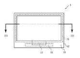
- FIG. 2 is a front view illustrating a schematic configuration of the display device with a touch panel according to the first embodiment.
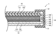
- 3 is an enlarged view of a cross section taken along line III-III in FIG.
- FIG. 4 is a cross-sectional view illustrating a schematic configuration of a display device with a touch panel according to a comparative example.
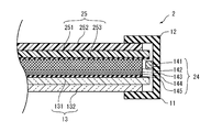
- FIG. 5 is sectional drawing which shows schematic structure of the display apparatus with a touchscreen concerning the 2nd Embodiment of this invention.
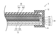
- FIG. 6 is sectional drawing which shows schematic structure of the display apparatus with a touchscreen concerning the 3rd Embodiment of this invention.
- FIG. 7 is sectional drawing which shows schematic structure of the display apparatus with a touchscreen concerning the 4th Embodiment of this invention.
- a display device with a touch panel includes a display panel capable of displaying an image, a touch panel disposed on a back side of a display surface of the display panel, and disposed between the display panel and the touch panel. And a backlight unit for irradiating the display panel with light.
- the touch panel blocks light irradiation of the backlight unit in a direction opposite to the display panel (first configuration).
- the touch panel is disposed on the back side of the display panel. Therefore, the operation area by a touch panel can be provided, keeping the area of the display panel large enough with respect to the area of the whole apparatus. Further, the luminance and display quality of the display panel are not affected.
- the touch panel is required to have translucency, but the above configuration does not require translucency. Therefore, various materials can be used for the members constituting the touch panel.
- the light in the back direction of the backlight unit (the direction opposite to the display panel) is blocked by the touch panel.
- the touch panel covers the entire surface of the backlight unit on the side opposite to the display panel (second configuration).
- the touch panel can more effectively shield the light from the backlight unit.
- the surface of the touch panel on the backlight unit side is preferably formed of a material having a reflectance with respect to visible light of 70% or more (third configuration).
- the touch panel also serves as a reflection sheet.
- this configuration it is possible to omit the reflection sheet from the backlight unit, and it is possible to reduce the number of parts and reduce the thickness of the entire apparatus.
- reflection includes not only specular reflection but also diffuse reflection.
- a preferable reflectance is 70% or more.
- a more preferable reflectance is 80% or more, and a more preferable reflectance is 95% or more.
- a material having a reflectance of 70% or more for visible light may be attached to the surface of the touch panel on the backlight unit side (fourth configuration).
- a material having a reflectance with respect to visible light of 70% or more may be applied or evaporated on the surface of the touch panel on the backlight unit side (fifth configuration).
- the reflective sheet can be omitted from the backlight unit, and the number of parts can be reduced. Moreover, since a base material becomes unnecessary compared with the case where a reflective sheet is provided independently, thickness can be made thin.
- the display panel may be a liquid crystal panel (sixth configuration).
- FIG. 1 is an exploded perspective view showing a schematic configuration of a display device 1 with a touch panel.
- FIG. 2 is a front view illustrating a schematic configuration of the display device 1 with a touch panel.
- 3 is an enlarged view of a cross section taken along line III-III in FIG.
- the display device 1 with a touch panel includes casings 11 and 12, a liquid crystal panel 13, a backlight unit 14, a touch panel 15, a drive circuit 16, and an FPC (Flexible Printed Circuit) 17.
- FPC Flexible Printed Circuit
- a touch panel 15 is disposed on the back side of the display surface of the liquid crystal panel 13.
- the operation surface of the touch panel 15 is provided on the side opposite to the display surface of the liquid crystal panel 13.
- a backlight unit 14 is disposed between the liquid crystal panel 13 and the touch panel 15. The backlight unit 14 is arranged to irradiate the liquid crystal panel 13 with light.
- the housings 11 and 12 contain a liquid crystal panel 13, a backlight unit 14, a touch panel 15, a drive circuit 16, and an FPC 17.
- the casings 11 and 12 are provided with openings 11a and 12a so that the display surface of the liquid crystal panel 13 and the operation surface of the touch panel 15 are exposed. Accordingly, the user can operate the touch panel 15 from the opening 12a while observing the liquid crystal panel 13 from the opening 11a.
- the liquid crystal panel 13 includes an active matrix substrate 131, a counter substrate 132, and a liquid crystal layer (not shown) sandwiched therebetween.
- the active matrix substrate 131 has a TFT array layer including switching elements such as TFTs (Thin Film Transistors), wirings, and the like on a glass substrate, although a detailed configuration is not illustrated.
- the active matrix substrate 131 includes a plurality of pixel electrodes arranged in a matrix.
- the counter substrate 132 includes a color filter and a counter electrode formed on the entire surface of the substrate.
- a polarizing plate may be provided on at least one surface of the liquid crystal panel 13.
- the liquid crystal panel 13 may be provided with various optical members such as a phase difference plate and a lens sheet.
- the driving method of the liquid crystal panel 13 is arbitrary.
- various types of liquid crystal display devices can be used as long as they are transmissive or transflective liquid crystal display devices that are irradiated with light from behind.
- the backlight unit 14 includes an LED light source 141, a light guide plate 142, prism sheets 143 and 144, a diffusion sheet 145, and a reflection sheet 146.
- the LED light source 141 is, for example, a white LED.
- the LED light sources 141 are arranged in a line.
- the light emitted from the LED light source 141 travels while being totally reflected in the light guide plate 142.
- the light guide plate 142 is made of, for example, acrylic, and a dot pattern is printed on the main surface opposite to the liquid crystal panel 13 side. Light traveling in the light guide plate 142 is scattered by the dot pattern and emitted to the outside of the light guide plate 142.
- the prism sheets 143 and 144 are disposed so as to overlap the front surface (the liquid crystal panel 13 side) of the light guide plate 142.
- the prism sheets 143 and 144 are formed, for example, by transferring a prism shape to a thermoplastic resin sheet with high pressure.
- the two prism sheets 143 and 144 are arranged so that their ridge lines are orthogonal to each other. As a result, both the horizontal and vertical components of the light emitted from the light guide plate 142 are condensed in the normal direction, and the luminance is improved.
- a diffusion sheet 145 is disposed on the front surface of the prism sheet 144.
- the diffusion sheet 145 is, for example, a polyethylene terephthalate film whose surface roughness is adjusted.
- the diffusion sheet 145 reduces uneven brightness of the backlight.
- the reflection sheet 146 is disposed on the back side (touch panel 15 side) of the light guide plate 142.
- the reflection sheet 146 reflects the light that has entered the light guide plate 142 on the back surface of the light guide plate 142.
- the reflection sheet 146 is preferably formed of a material having high reflectivity in order to suppress light attenuation and efficiently use light.
- polyester, polycarbonate, porous polypropylene having a large number of air bubbles, finely foamed polyester, or the like can be used.
- a specular reflection type reflection sheet made of a silver thin film or the like may be used.
- the structure using the LED light source 141 and the light-guide plate 142 as the backlight unit 14 was demonstrated here.
- this configuration is merely an example, and a cold cathode tube may be used instead of the LED light source 141, or a direct type configuration without using the light guide plate 142 may be used.
- the configuration of the prism sheets 143 and 144, the diffusion sheet 145, and the like described above is not limited to this.
- These optical sheets can have various configurations and combinations other than those exemplified above.
- a total reflection type prism sheet may be used as the prism sheet.
- the diffusion sheet may be disposed on the light guide plate side with respect to the prism sheet. Further, a plurality of diffusion sheets may be arranged, or a part of the prism sheet or the diffusion sheet may be omitted.
- the touch panel 15 includes two substrates 151 and 152. Although a detailed configuration is not shown in the touch panel 15, both a resistive film type and a capacitance type can be adopted.
- the substrates 151 and 152 are opposed to each other via a spacer. Electrode films are formed on the opposing surfaces of the substrates 151 and 152, respectively.
- the electrode film formed on the substrate 151 and the electrode film formed on the substrate 152 come into contact with each other at the pressed position.
- the position touched by a finger or the like can be calculated.
- the touch panel 15 is a capacitive type
- an electrode film is formed between the substrates 151 and 152.
- an electric capacity is formed through the substrate 152 between the finger or the like and the electrode film. By measuring the change in the electric capacity, it is possible to calculate the position where the finger or the like is in contact.
- the touch panel 15 may be a surface-type capacitance method or a projection-type capacitance method.
- the substrates 151 and 152 may be provided with insulating properties.
- the touch panel 15 is not required to have translucency. Therefore, various materials can be used for the substrates 151 and 152. Further, the electrode film does not need to use a transparent conductive film, and various conductive materials can be used.
- the drive circuit 16 drives the liquid crystal panel 13 and the touch panel 15.
- the drive circuit 16 is connected to the liquid crystal panel 13 and the touch panel 15 via the FPC 17.
- the drive circuit 16 may also serve as a drive circuit for the backlight unit 14 and other elements (not shown) of the display device 1.
- FIG. 4 is a cross-sectional view schematically showing the configuration of the display device 9 with a touch panel according to the comparative example.
- the display device 9 with a touch panel includes housings 11 and 12, a liquid crystal panel 13, a backlight unit 14, a touch panel 95, and a back metal plate 98.
- the display device 9 with a touch panel includes a drive circuit and an FPC, like the display device 1 with a touch panel.
- the touch panel 95 is disposed on the front surface of the liquid crystal panel 13, that is, on the surface closer to the observer side than the liquid crystal panel 13. Therefore, the substrates 951 and 952 that form the touch panel 95 need to be formed of a light-transmitting material.
- the substrates 951 and 952 are typically made of glass or transparent plastic film or a combination thereof.
- the transmittance is about 90% at the maximum, and a decrease in luminance of the liquid crystal panel 13 cannot be avoided.
- the touch panel 15 is disposed on the back surface of the liquid crystal panel 13. Therefore, the luminance and display quality of the liquid crystal panel 13 are not affected.
- the area of the liquid crystal panel 13 and the area of the touch panel 15 can be sufficiently increased with respect to the entire area of the display device 1 with a touch panel. Thereby, both a large display area and excellent operability are achieved.
- the touch panel 15 includes a structural member that reinforces the back side of the display device 1 with a touch panel, a light shielding member that shields light leaking from the backlight unit 14, and the backlight unit 14. Also serves as a role. This eliminates the need for the back surface metal plate 98 and the like, and can reduce the number of parts and reduce the thickness of the entire apparatus.
- the transmittance of the touch panel 15 is desirably low. By making the transmittance of the touch panel 15 low, the light leaking from the reflection sheet 146 of the backlight unit 14 can be more effectively shielded.
- a preferable transmittance of the touch panel 15 is 50% or less.
- a more preferable transmittance is 10% or less.
- the substrates 151 and 152 or the electrode film forming the touch panel 15 may be formed of a material having a low transmittance. Further, even when the transmittance of the substrate 151 or 152 is not low, a material with low transmittance may be attached to the surface of the substrate 151 or 152, applied, or evaporated.
- the touch panel 15 covers the entire surface of the backlight unit 14 on the reflective sheet 146 side.
- FIG. 5 is sectional drawing which shows typically the structure of the display apparatus 2 with a touchscreen concerning the 2nd Embodiment of this invention.
- the display device 2 with a touch panel includes housings 11 and 12, a liquid crystal panel 13, a backlight unit 24, and a touch panel 25.
- the display device 2 with a touch panel includes a drive circuit and an FPC similarly to the display device 1 with a touch panel.
- the backlight unit 24 includes a plurality of LED light sources 141, a light guide plate 142, prism sheets 143 and 144, and a diffusion sheet 145. Compared with the backlight unit 14, the backlight unit 24 omits the reflection sheet.
- the touch panel 25 includes two substrates 251 and 252.
- a reflective layer 253 made of a highly reflective material is formed on the surface of the substrate 251 on the backlight unit 24 side.
- the reflective layer 253 can be provided by adhering, for example, polyester or polycarbonate, porous polypropylene having a large number of air bubbles, finely foamed polyester, or the like to the substrate 251.
- a coating material in which these resins or metal fine particles such as silver and aluminum are dispersed can be applied and provided.
- it can also provide by vapor-depositing metals, such as silver and aluminum, or a metal oxide.
- the preferable reflectance of the reflective layer 253 is 70% or more. A more preferable reflectance is 80% or more. A more preferable reflectance is 95% or more.
- the touch panel 25 also serves as a reflection sheet.
- a reflective sheet can be omitted from the backlight unit 24, and the number of parts can be reduced.
- a base material becomes unnecessary compared with the case where a reflective sheet is provided independently, thickness can be made thin.
- FIG. 6 is sectional drawing which shows typically the structure of the display apparatus 3 with a touchscreen concerning the 3rd Embodiment of this invention.
- the display device 3 with a touch panel includes housings 11 and 12, a liquid crystal panel 13, a backlight unit 24, and a touch panel 35.
- the display device with a touch panel 3 includes a drive circuit and an FPC, like the display device with a touch panel 1.
- the touch panel 35 includes two substrates 351 and 352.
- the substrate 351 on the backlight unit 24 side is formed of a material having high reflectivity.
- the substrate 351 is made of, for example, polyester or polycarbonate, porous polypropylene having a large number of bubbles inside, or finely foamed polyester.
- the preferable reflectance of the substrate 351 is 70% or more. A more preferable reflectance is 80% or more. A more preferable reflectance is 95% or more.
- the touch panel 35 also serves as a reflection sheet.
- a reflective sheet can be omitted from the backlight unit 24, and the number of parts can be reduced.
- thickness can be made thin.
- FIG. 7 is sectional drawing which shows typically the structure of the display apparatus 4 with a touch panel concerning the 4th Embodiment of this invention.
- the display device 4 with a touch panel includes housings 11 and 42, a liquid crystal panel 13, a backlight unit 14, and a touch panel 45.
- the display device 4 with a touch panel includes a drive circuit and an FPC, like the display device 1 with a touch panel.
- the touch panel 45 includes substrates 451 and 452 having different sizes.
- the substrate 451 on the backlight unit 24 side is formed in substantially the same area as the backlight unit 14.
- the substrate 452 on the operation surface side is formed slightly smaller than the substrate 451.
- the casing 42 on the touch panel 45 side has the same thickness as the substrate 452 so as to flatten the operation surface.
- the size of the operation surface of the touch panel 45 can be changed while the light shielding function by the touch panel 45 is provided. Thereby, the variation of the display apparatus with a touch panel is obtained.
- the second embodiment in which the reflective layer is provided on the touch panel substrate and the fourth embodiment in which the size of the touch panel on the operation surface side is changed.
- the third embodiment in which the touch panel substrate is formed of a highly reflective material and the fourth embodiment in which the size of the touch panel on the operation surface side is changed.
- the present invention can be industrially used as a display device with a touch panel provided with a backlight.
Landscapes
- Engineering & Computer Science (AREA)
- General Engineering & Computer Science (AREA)
- Theoretical Computer Science (AREA)
- Human Computer Interaction (AREA)
- Physics & Mathematics (AREA)
- General Physics & Mathematics (AREA)
- Position Input By Displaying (AREA)
- Liquid Crystal (AREA)
Abstract
大きな表示領域と、優れた操作性とを両立し、かつ、表示装置の輝度および表示品位に影響を及ぼさないタッチパネル付き表示装置の構成を得る。タッチパネル付き表示装置(1)は、画像を表示可能な表示パネル(13)と、前記表示パネル(13)の表示面の背面側に配置されたタッチパネル(15)と、前記表示パネル(13)と前記タッチパネル(15)との間に配置され、前記表示パネル(13)に光を照射するバックライトユニット(14)とを備える。前記タッチパネル(15)は、前記バックライトユニット(14)の、前記表示パネル(13)と反対方向への光の照射を遮っている。
Description
本発明は、タッチパネル付き表示装置に関し、より詳しくはバックライトを備えたタッチパネル付き表示装置に関する。
スマートフォンや電子書籍端末等の薄型表示装置が、広く利用されている。これらの機器では、大きな表示領域と、優れた操作性とを両立するため、表示パネルの上にタッチパネルを重ねた構成がとられている。しかし、表示パネルとタッチパネルとを重ねることで、表示パネルの輝度が低下する。また、表示パネルとタッチパネルとの間で干渉縞が発生するなど、表示品位の悪化が起こる。
特開2000-278391号公報には、移動体端末装置の背面にタッチパネルを備え、前記タッチパネルから手書き入力された文字を認識する手段を備えたことを特徴とする移動体端末装置が開示されている。
上記の文献には、装置の背面にタッチパネルを搭載することが記載されているが、その具体的な構成は開示されていない。
本発明の目的は、大きな表示領域と、優れた操作性とを両立し、かつ、表示パネルの輝度および表示品位に影響を及ぼさないタッチパネル付き表示装置の構成を得ることである。
以下に開示するタッチパネル付き表示装置は、画像を表示可能な表示パネルと、前記表示パネルの表示面の背面側に配置されたタッチパネルと、前記表示パネルと前記タッチパネルとの間に配置され、前記表示パネルに光を照射するバックライトユニットとを備える。前記タッチパネルは、前記バックライトユニットの、前記表示パネルと反対方向への光の照射を遮っている。
本発明によれば、大きな表示領域と、優れた操作性とを両立し、かつ、表示パネルの輝度および表示品位に影響を及ぼさないタッチパネル付き表示装置の構成が得られる。
本発明の一実施形態にかかるタッチパネル付き表示装置は、画像を表示可能な表示パネルと、前記表示パネルの表示面の背面側に配置されたタッチパネルと、前記表示パネルと前記タッチパネルとの間に配置され、前記表示パネルに光を照射するバックライトユニットとを備える。前記タッチパネルは、前記バックライトユニットの、前記表示パネルと反対方向への光の照射を遮っている(第1の構成)。
この構成によれば、タッチパネルは、表示パネルの背面側に配置される。これにより、機器全体の面積に対する表示パネルの面積を十分に大きく保ったままで、タッチパネルによる操作領域を設けることができる。また、表示パネルの輝度および表示品位に影響を及ぼすことがない。
また、従来の構成では、タッチパネルには透光性が求められていたが、上記の構成では透光性は不要である。したがって、タッチパネルを構成する各部材の材料は種々のものを採用できる。
上記の構成では、タッチパネルにより、バックライトユニットの背面方向(表示パネルと反対方向)への光が遮蔽される。これにより、バックライトユニット背面の遮蔽部材等が不要になり、部品点数の削減および装置全体の薄型化を実現できる。
前記第1の構成において、前記タッチパネルは、前記バックライトユニットの、前記表示パネルと反対側の面全体を覆っていることが好ましい(第2の構成)。
上記の構成によれば、タッチパネルが、バックライトユニットからの光をより効果的に遮蔽できる。
前記第1または第2の構成において、前記タッチパネルのバックライトユニット側の表面は、可視光に対する反射率が70%以上である材料で形成されていることが好ましい(第3の構成)。
上記の構成によれば、タッチパネルが、反射シートの役割を兼ねる。この構成により、バックライトユニットから反射シートを省くことができ、部品点数の削減および装置全体の薄型化を実現できる。
なお、上記の「反射」の用語は、鏡面反射のみではなく、拡散反射を含む。好ましい反射率は70%以上である。より好ましい反射率は80%以上であり、さらに好ましい反射率は95%以上である。
前記第1または第2の構成において、前記タッチパネルのバックライトユニット側の表面に、可視光に対する反射率が70%以上である材料が貼着されていても良い(第4の構成)。
前記第1または第2の構成において、前記タッチパネルのバックライトユニット側の表面に、可視光に対する反射率が70%以上である材料が塗布または蒸着されていても良い(第5の構成)。
上記第4または第5の構成によっても、バックライトユニットから反射シートを省くことができ、部品点数を削減できる。また、独立して反射シートを設けた場合と比較して、基材が不要となるため厚さを薄くできる。
前記第1~第5のいずれかの構成において、前記表示パネルは、液晶パネルであっても良い(第6の構成)。
[実施の形態]
以下、図面を参照し、本発明の実施の形態を詳しく説明する。図中同一または相当部分には同一符号を付してその説明は繰り返さない。なお、説明を分かりやすくするために、以下で参照する図面においては、構成が簡略化または模式化して示されたり、一部の構成部材が省略されたりしている。また、各図に示された構成部材間の寸法比は、必ずしも実際の寸法比を示すものではない。
以下、図面を参照し、本発明の実施の形態を詳しく説明する。図中同一または相当部分には同一符号を付してその説明は繰り返さない。なお、説明を分かりやすくするために、以下で参照する図面においては、構成が簡略化または模式化して示されたり、一部の構成部材が省略されたりしている。また、各図に示された構成部材間の寸法比は、必ずしも実際の寸法比を示すものではない。
[第1の実施形態]
図1~図3を用いて、本発明の第1の実施形態にかかるタッチパネル付き表示装置1を説明する。図1は、タッチパネル付き表示装置1の概略構成を示す分解斜視図である。図2は、タッチパネル付き表示装置1の概略構成を示す正面図である。図3は、図2におけるIII-III線に沿った断面の拡大図である。
図1~図3を用いて、本発明の第1の実施形態にかかるタッチパネル付き表示装置1を説明する。図1は、タッチパネル付き表示装置1の概略構成を示す分解斜視図である。図2は、タッチパネル付き表示装置1の概略構成を示す正面図である。図3は、図2におけるIII-III線に沿った断面の拡大図である。
タッチパネル付き表示装置1は、筐体11,12、液晶パネル13、バックライトユニット14、タッチパネル15、駆動回路16、FPC(Flexible Printed Circuit:フレキシブルプリント基板)17を備えている。
タッチパネル付き表示装置1では、液晶パネル13の表示面の背面側に、タッチパネル15が配置されている。タッチパネル15の操作面は、液晶パネル13の表示面と反対側に設けられている。液晶パネル13とタッチパネル15との間には、バックライトユニット14が配置されている。バックライトユニット14は、液晶パネル13に光を照射するように配置されている。
筐体11および12は、液晶パネル13、バックライトユニット14、タッチパネル15、駆動回路16、およびFPC17を収容している。筐体11および12には、液晶パネル13の表示面およびタッチパネル15の操作面が露出するように、開口11aおよび12aが設けられている。これにより、ユーザは、開口11aから液晶パネル13を観察しながら、開口12aからタッチパネル15を操作することができる。
液晶パネル13は、アクティブマトリクス基板131と、対向基板132と、これらに挟持された液晶層(図示せず)とを備えている。
アクティブマトリクス基板131は、詳しい構成は図示していないが、ガラス基板上に、TFT(Thin Film Transistor:薄膜トランジスタ)等のスイッチング素子や配線等を含むTFTアレイ層を有している。また、アクティブマトリクス基板131は、マトリクス状に配置された複数の画素電極を有している。対向基板132は、詳しい構成は図示していないが、カラーフィルタと、基板全面に形成された対向電極とを有している。また、液晶パネル13の少なくとも一方の表面に偏光板を設けても良い。また、この他に、液晶パネル13には、位相差板やレンズシート等の各種の光学部材を設けても良い。
なお、液晶パネル13の駆動方法は任意である。液晶パネル13として、後方からバックライトにより光が照射される、透過型または半透過型の液晶表示装置であれば、様々な方式の液晶表示装置を用いることができる。
バックライトユニット14は、LED光源141、導光板142、プリズムシート143,144、拡散シート145、および反射シート146を備えている。
LED光源141は、例えば白色LEDである。LED光源141は、一列に整列して配置されている。LED光源141から発せられた光は、導光板142内を全反射しながら進む。導光板142は、例えばアクリル製で、液晶パネル13側と反対側の主面にはドットパターンが印刷されている。導光板142内を進む光は、このドットパターンに散乱されて、導光板142の外部へ出射される。
プリズムシート143,144は、導光板142の前面(液晶パネル13側)に重ねて配置されている。プリズムシート143,144は、例えば、熱可塑性樹脂シートにプリズム形状を高圧力で転写して形成される。2枚のプリズムシート143,144はその稜線が互いに直交するように配置されている。これにより、導光板142から出射された光は、水平および垂直成分がともに法線方向へ集光され、輝度が向上する。
プリズムシート144の前面には、拡散シート145が配置されている。拡散シート145は、例えば、表面の粗さを調整したポリエチレンテレフタレート製のフィルムである。拡散シート145は、バックライトの輝度ムラを低減する。
反射シート146は、導光板142の背面側(タッチパネル15側)に配置されている。反射シート146は、導光板142内に進入した光を、導光板142の背面において反射させる。反射シート146は、光の減衰を抑えて光を効率よく利用するため、反射率の高い材料で形成されていることが望ましい。反射シート146は、例えば、ポリエステルやポリカーボネート、内部に多数の気泡を有する多孔質ポリプロピレンや微細発泡ポリエステル等を用いることができる。また、このような拡散反射型の反射シートに替えて、銀薄膜等による鏡面反射型の反射シートを用いることもできる。
なお、ここではバックライトユニット14として、LED光源141および導光板142を用いた構成を説明した。しかし、この構成は例示であって、LED光源141に替えて冷陰極管を使用しても良いし、導光板142を用いない直下型の構成としても良い。
また、上述したプリズムシート143,144、拡散シート145等の構成も、これに限定されない。これらの光学シート類については、上で例示した以外にも様々な構成や組み合わせが可能である。例えば、プリズムシートとして、上述した屈折型のプリズムシートに替えて、全反射型のプリズムシートを用いても良い。また、拡散シートを、プリズムシートよりも導光板側に配置しても良い。さらに、拡散シートを複数配置しても良いし、プリズムシートや拡散シートの一部を省いても良い。
タッチパネル15は、2枚の基板151および152を備えている。タッチパネル15は、詳しい構成を図示していないが、抵抗膜方式および静電容量方式の、いずれも採用することができる。
例えば、タッチパネル15が抵抗膜方式の場合には、基板151および152は、スペーサを介して対向している。基板151および152の、向かい合う面にはそれぞれ電極膜が形成されている。操作面側の基板152を手指等で押圧することにより、押圧された箇所で基板151に形成された電極膜と基板152に形成された電極膜とが接触する。このときの抵抗分圧を測定することにより、手指等が触れた位置を算出することができる。
また、タッチパネル15が静電容量方式の場合には、基板151と152との間に電極膜が形成されている。操作面側の基板152に手指等が接触すると、手指等と電極膜との間に、基板152を介して電気容量が形成される。この電気容量の変化を測定することにより、手指等が接触した位置を算出することができる。なお、タッチパネル15は、表面型の静電容量方式であっても良いし、投影型の静電容量方式であっても良い。
抵抗膜方式と静電容量方式とのいずれの場合も、基板151および152は、絶縁性を備えていれば良い。本発明では、タッチパネル15は透光性を要求されない。したがって、基板151および152として、種々の材料を用いることができる。また、電極膜も、透明導電膜を用いる必要はなく、導電性のある種々の材料を用いることができる。
駆動回路16は、液晶パネル13およびタッチパネル15を駆動する。駆動回路16は、液晶パネル13およびタッチパネル15と、FPC17を介して接続されている。駆動回路16は、バックライトユニット14や、表示装置1の図示しないその他の要素の駆動回路を兼ねる構成としても良い。
以上、本発明の第1の実施形態にかかるタッチパネル付き表示装置1の構成について説明した。ここで、本発明の効果を説明するための仮想的な比較例について説明する。
図4は、比較例にかかるタッチパネル付き表示装置9の構成を模式的に示す断面図である。タッチパネル付き表示装置9は、筐体11,12、液晶パネル13、バックライトユニット14、タッチパネル95、および裏面板金98を備えている。なお、図4には図示していないが、タッチパネル付き表示装置9は、タッチパネル付き表示装置1と同様に、駆動回路とFPCとを備えている。
タッチパネル95は、液晶パネル13の前面、すなわち、液晶パネル13よりも観察者側に近い面に配置されている。したがって、タッチパネル95を形成する基板951および952は、透光性の材料で形成されている必要がある。基板951および952は、典型的にはガラスもしくは透明のプラスチックフィルムまたはこれらの組み合わせが採用される。
透光性の材料でタッチパネル95を形成したとしても、その透過率は最高でも90%程度であり、液晶パネル13の輝度の低下は避けることができない。タッチパネル95を薄くして透過率を上げることも、信頼性の点から限界がある。さらに、タッチパネル95と液晶パネル13との間で干渉縞が発生するなどの問題もある。
また、この構成では、タッチパネル付き表示装置9の裏面側を補強するとともに、バックライトユニット14の反射シート146から漏れ出す光を遮蔽するために裏面板金98を設ける必要があった。
一方、本発明の第1の実施形態にかかるタッチパネル付き表示装置1によれば、タッチパネル15は、液晶パネル13の背面に配置される。そのため、液晶パネル13の輝度および表示品位に影響を及ぼすことがない。
また、タッチパネル付き表示装置1全体の面積に対して、液晶パネル13の面積およびタッチパネル15の面積を十分に大きくすることができる。これにより、大きな表示領域と、優れた操作性とを両立している。
また、本実施形態では、タッチパネル15が、タッチパネル付き表示装置1の裏面側を補強する構造部材、バックライトユニット14から漏れ出す光を遮蔽する遮光部材、およびバックライトユニット14等を収容するケースとしての役割を兼ねる。これにより裏面板金98等が不要になり、部品点数の削減および装置全体の薄型化を実現できる。
なお、タッチパネル15の透過率は低いことが望ましい。タッチパネル15の透過率を低くすることにより、バックライトユニット14の反射シート146から漏れ出す光をより効果的に遮蔽できる。タッチパネル15の好ましい透過率は、50%以下である。より好ましい透過率は10%以下である。
なお、タッチパネル15の透過率を下げるためには、タッチパネル15を形成する基板151、152または電極膜を透過率の低い材料で形成すれば良い。また、基板151または152の透過率が低くなくても、基板151または152の表面に、透過率の低い材料を貼着したり、塗布したり、蒸着しても良い。
また、タッチパネル15が、バックライトユニット14の、反射シート146側の面全体を覆っていることが望ましい。そのためには、基板151および152の少なくとも一方が、バックライトユニット14と同じか、より大きな面積を有していれば良い。これにより、バックライトユニット14から漏れ出す光をより効果的に遮蔽できる
[第2の実施形態]
図5は、本発明の第2の実施形態にかかるタッチパネル付き表示装置2の構成を模式的に示す断面図である。タッチパネル付き表示装置2は、筐体11,12、液晶パネル13、バックライトユニット24、およびタッチパネル25を備えている。なお、図5には図示していないが、タッチパネル付き表示装置2は、タッチパネル付き表示装置1と同様に、駆動回路とFPCとを備えている。
図5は、本発明の第2の実施形態にかかるタッチパネル付き表示装置2の構成を模式的に示す断面図である。タッチパネル付き表示装置2は、筐体11,12、液晶パネル13、バックライトユニット24、およびタッチパネル25を備えている。なお、図5には図示していないが、タッチパネル付き表示装置2は、タッチパネル付き表示装置1と同様に、駆動回路とFPCとを備えている。
バックライトユニット24は、複数のLED光源141、導光板142、プリズムシート143,144、および拡散シート145を備えている。バックライトユニット24は、バックライトユニット14と比べて、反射シートが省かれている。
タッチパネル25は、2枚の基板251および252を備えている。そして、基板251のバックライトユニット24側の表面には、反射率の高い材料からなる反射層253が形成されている。
反射層253は、例えば、ポリエステルやポリカーボネート、内部に多数の気泡を有する多孔質ポリプロピレンや微細発泡ポリエステル等を、基板251に貼着して設けることができる。あるいは、これらの樹脂、または銀やアルミニウム等の金属微粒子を分散させた塗料を塗布して設けることができる。さらに、銀やアルミニウム等の金属または金属酸化物を蒸着することにより設けることもできる。
反射層253の好ましい反射率は70%以上である。より好ましい反射率は80%以上である。さらに好ましい反射率は95%以上である。
本実施形態によれば、タッチパネル25が、反射シートを兼ねる。これにより、バックライトユニット24から反射シートを省くことができ、部品点数を削減できる。また、独立して反射シートを設ける場合と比較して、基材が不要となるため、厚みを薄くできる。
[第3の実施形態]
図6は、本発明の第3の実施形態にかかるタッチパネル付き表示装置3の構成を模式的に示す断面図である。タッチパネル付き表示装置3は、筐体11,12、液晶パネル13、バックライトユニット24、およびタッチパネル35を備えている。なお、図6には図示していないが、タッチパネル付き表示装置3は、タッチパネル付き表示装置1と同様に、駆動回路とFPCとを備えている。
図6は、本発明の第3の実施形態にかかるタッチパネル付き表示装置3の構成を模式的に示す断面図である。タッチパネル付き表示装置3は、筐体11,12、液晶パネル13、バックライトユニット24、およびタッチパネル35を備えている。なお、図6には図示していないが、タッチパネル付き表示装置3は、タッチパネル付き表示装置1と同様に、駆動回路とFPCとを備えている。
タッチパネル35は、2枚の基板351および352を備えている。そして、バックライトユニット24側の基板351は、反射率の高い材料により形成されている。基板351は、例えば、ポリエステルやポリカーボネート、内部に多数の気泡を有する多孔質ポリプロピレンや微細発泡ポリエステル等で形成されている。
基板351の好ましい反射率は70%以上である。より好ましい反射率は80%以上である。さらに好ましい反射率は95%以上である。
本実施形態によれば、タッチパネル35が、反射シートを兼ねる。これにより、バックライトユニット24から反射シートを省くことができ、部品点数を削減できる。また、独立して反射シートを設ける場合と比較して、厚みを薄くできる。
[第4の実施形態]
図7は、本発明の第4の実施形態にかかるタッチパネル付き表示装置4の構成を模式的に示す断面図である。タッチパネル付き表示装置4は、筐体11,42、液晶パネル13、バックライトユニット14、およびタッチパネル45を備えている。なお、図7には図示していないが、タッチパネル付き表示装置4は、タッチパネル付き表示装置1と同様に、駆動回路とFPCとを備えている。
図7は、本発明の第4の実施形態にかかるタッチパネル付き表示装置4の構成を模式的に示す断面図である。タッチパネル付き表示装置4は、筐体11,42、液晶パネル13、バックライトユニット14、およびタッチパネル45を備えている。なお、図7には図示していないが、タッチパネル付き表示装置4は、タッチパネル付き表示装置1と同様に、駆動回路とFPCとを備えている。
タッチパネル45は、大きさの異なる基板451および452を備えている。バックライトユニット24側の基板451は、バックライトユニット14とほぼ同じ面積に形成されている。操作面側の基板452は、基板451よりも一回り小さく形成されている。
タッチパネル45側の筐体42は、操作面を平坦にするように、基板452と厚みが揃えられている。
本実施形態によれば、タッチパネル45による遮光機能を持たせたまま、タッチパネル45の操作面の大きさを変えることができる。これにより、タッチパネル付き表示装置のバリエーションが得られる。
[その他の実施形態]
以上、本発明についての実施形態を説明したが、本発明は上述の各実施形態のみに限定されず、発明の範囲内で種々の変更が可能である。また、上述した各実施形態は、適宜組み合わせて実施が可能である。
以上、本発明についての実施形態を説明したが、本発明は上述の各実施形態のみに限定されず、発明の範囲内で種々の変更が可能である。また、上述した各実施形態は、適宜組み合わせて実施が可能である。
例えば、タッチパネルの基板に反射層を設けた第2の実施形態と、操作面側のタッチパネルの大きさを変えた第4の実施形態とを組み合わせることが可能である。また、タッチパネルの基板を反射率の高い材料で形成した第3の実施形態と、操作面側のタッチパネルの大きさを変えた第4の実施形態とを組み合わせることが可能である。
本発明は、バックライトを備えたタッチパネル付き表示装置として産業上の利用が可能である。
Claims (6)
- 画像を表示可能な表示パネルと、
前記表示パネルの表示面の背面側に配置されたタッチパネルと、
前記表示パネルと前記タッチパネルとの間に配置され、前記表示パネルに光を照射するバックライトユニットとを備え、
前記タッチパネルは、前記バックライトユニットの、前記表示パネルと反対方向への光の照射を遮っている、タッチパネル付き表示装置。 - 前記タッチパネルは、前記バックライトユニットの、前記表示パネルと反対側の面全体を覆っている、請求項1に記載のタッチパネル付き表示装置。
- 前記タッチパネルのバックライトユニット側の表面は、可視光に対する反射率が70%以上である材料で形成されている、請求項1また2に記載のタッチパネル付き表示装置。
- 前記タッチパネルのバックライトユニット側の表面に、可視光に対する反射率が70%以上である材料が貼着されている、請求項1または2に記載のタッチパネル付き表示装置。
- 前記タッチパネルのバックライトユニット側の表面に、可視光に対する反射率が70%以上である材料が塗布または蒸着されている、請求項1または2に記載のタッチパネル付き表示装置。
- 前記表示パネルは、液晶パネルである、請求項1~5のいずれか一項に記載のタッチパネル付き表示装置。
Applications Claiming Priority (2)
| Application Number | Priority Date | Filing Date | Title |
|---|---|---|---|
| JP2011-173192 | 2011-08-08 | ||
| JP2011173192A JP2014199474A (ja) | 2011-08-08 | 2011-08-08 | タッチパネル付き表示装置 |
Publications (1)
| Publication Number | Publication Date |
|---|---|
| WO2013021972A1 true WO2013021972A1 (ja) | 2013-02-14 |
Family
ID=47668479
Family Applications (1)
| Application Number | Title | Priority Date | Filing Date |
|---|---|---|---|
| PCT/JP2012/070009 Ceased WO2013021972A1 (ja) | 2011-08-08 | 2012-08-06 | タッチパネル付き表示装置 |
Country Status (2)
| Country | Link |
|---|---|
| JP (1) | JP2014199474A (ja) |
| WO (1) | WO2013021972A1 (ja) |
Families Citing this family (1)
| Publication number | Priority date | Publication date | Assignee | Title |
|---|---|---|---|---|
| CN118829825A (zh) * | 2022-03-28 | 2024-10-22 | 株式会社小糸制作所 | 支架构件以及车辆用灯具 |
Citations (8)
| Publication number | Priority date | Publication date | Assignee | Title |
|---|---|---|---|---|
| JPS63171837U (ja) * | 1987-04-28 | 1988-11-08 | ||
| JPH09265350A (ja) * | 1996-03-28 | 1997-10-07 | Canon Inc | ペン入力表示方法とその装置 |
| JP2004272365A (ja) * | 2003-03-05 | 2004-09-30 | Seiko Epson Corp | 電気光学パネル、電気光学装置、電気光学パネルの製造方法、電気光学装置の製造方法および電磁誘導センサ、並びに電子機器 |
| JP2004302433A (ja) * | 2003-03-28 | 2004-10-28 | Lg Philips Lcd Co Ltd | デジタイザが装着された液晶表示装置 |
| JP2006260366A (ja) * | 2005-03-18 | 2006-09-28 | Sanyo Epson Imaging Devices Corp | 表示装置及び電子機器 |
| JP2007041760A (ja) * | 2005-08-02 | 2007-02-15 | Nec Lcd Technologies Ltd | 液晶表示装置 |
| JP2009086752A (ja) * | 2007-09-27 | 2009-04-23 | Seiko Precision Inc | 照光式タッチパネル及び照光式タッチパネルの製造方法 |
| JP2009199558A (ja) * | 2008-02-25 | 2009-09-03 | Wacom Co Ltd | 表示機能付き入力装置 |
-
2011
- 2011-08-08 JP JP2011173192A patent/JP2014199474A/ja not_active Withdrawn
-
2012
- 2012-08-06 WO PCT/JP2012/070009 patent/WO2013021972A1/ja not_active Ceased
Patent Citations (8)
| Publication number | Priority date | Publication date | Assignee | Title |
|---|---|---|---|---|
| JPS63171837U (ja) * | 1987-04-28 | 1988-11-08 | ||
| JPH09265350A (ja) * | 1996-03-28 | 1997-10-07 | Canon Inc | ペン入力表示方法とその装置 |
| JP2004272365A (ja) * | 2003-03-05 | 2004-09-30 | Seiko Epson Corp | 電気光学パネル、電気光学装置、電気光学パネルの製造方法、電気光学装置の製造方法および電磁誘導センサ、並びに電子機器 |
| JP2004302433A (ja) * | 2003-03-28 | 2004-10-28 | Lg Philips Lcd Co Ltd | デジタイザが装着された液晶表示装置 |
| JP2006260366A (ja) * | 2005-03-18 | 2006-09-28 | Sanyo Epson Imaging Devices Corp | 表示装置及び電子機器 |
| JP2007041760A (ja) * | 2005-08-02 | 2007-02-15 | Nec Lcd Technologies Ltd | 液晶表示装置 |
| JP2009086752A (ja) * | 2007-09-27 | 2009-04-23 | Seiko Precision Inc | 照光式タッチパネル及び照光式タッチパネルの製造方法 |
| JP2009199558A (ja) * | 2008-02-25 | 2009-09-03 | Wacom Co Ltd | 表示機能付き入力装置 |
Also Published As
| Publication number | Publication date |
|---|---|
| JP2014199474A (ja) | 2014-10-23 |
Similar Documents
| Publication | Publication Date | Title |
|---|---|---|
| JP4450089B2 (ja) | タッチパネル及び電気光学装置 | |
| KR100982117B1 (ko) | 터치 패널, 전기 광학 장치 및 전자기기 | |
| CN204595380U (zh) | 面板结构和显示装置 | |
| CN101965604B (zh) | 显示装置 | |
| CN104597653B (zh) | 显示面板和显示装置 | |
| CN101840089A (zh) | 触控式显示装置 | |
| JP2013168172A (ja) | 薄型タッチ装置 | |
| KR102125906B1 (ko) | 액정 표시 장치 | |
| CN103970336A (zh) | 触控显示面板及触控显示装置 | |
| JP2015079095A (ja) | 電装機器 | |
| CN101859206A (zh) | 触控式显示装置 | |
| TWI475309B (zh) | 電子紙顯示器 | |
| CN110618761B (zh) | 位置输入装置和带位置输入功能的显示装置 | |
| TWI395003B (zh) | 液晶顯示裝置 | |
| EP4040275A1 (en) | Touch display device | |
| JP2001075075A (ja) | 液晶装置、および電子機器 | |
| CN116964517A (zh) | 防窥显示装置 | |
| JP2011209690A (ja) | 液晶表示装置 | |
| WO2013021972A1 (ja) | タッチパネル付き表示装置 | |
| CN100529845C (zh) | 双面显示器及改善其显示画面的方法 | |
| CN105183210A (zh) | 显示屏组件及终端 | |
| JP2017211465A (ja) | 液晶表示装置 | |
| JP2017026999A (ja) | 表示装置 | |
| KR102637199B1 (ko) | 보더리스타입 표시장치 | |
| JP5271729B2 (ja) | 入力機能付表示装置、および電子機器 |
Legal Events
| Date | Code | Title | Description |
|---|---|---|---|
| 121 | Ep: the epo has been informed by wipo that ep was designated in this application |
Ref document number: 12821881 Country of ref document: EP Kind code of ref document: A1 |
|
| NENP | Non-entry into the national phase |
Ref country code: DE |
|
| 122 | Ep: pct application non-entry in european phase |
Ref document number: 12821881 Country of ref document: EP Kind code of ref document: A1 |
|
| NENP | Non-entry into the national phase |
Ref country code: JP |