WO2013018583A1 - 光子出力装置、光子出力方法、及び光子出力装置に用いる半導体の製造方法 - Google Patents
光子出力装置、光子出力方法、及び光子出力装置に用いる半導体の製造方法 Download PDFInfo
- Publication number
- WO2013018583A1 WO2013018583A1 PCT/JP2012/068684 JP2012068684W WO2013018583A1 WO 2013018583 A1 WO2013018583 A1 WO 2013018583A1 JP 2012068684 W JP2012068684 W JP 2012068684W WO 2013018583 A1 WO2013018583 A1 WO 2013018583A1
- Authority
- WO
- WIPO (PCT)
- Prior art keywords
- diamond layer
- type diamond
- output device
- photon output
- photon
- Prior art date
- Legal status (The legal status is an assumption and is not a legal conclusion. Google has not performed a legal analysis and makes no representation as to the accuracy of the status listed.)
- Ceased
Links
Images







Classifications
-
- H—ELECTRICITY
- H10—SEMICONDUCTOR DEVICES; ELECTRIC SOLID-STATE DEVICES NOT OTHERWISE PROVIDED FOR
- H10H—INORGANIC LIGHT-EMITTING SEMICONDUCTOR DEVICES HAVING POTENTIAL BARRIERS
- H10H20/00—Individual inorganic light-emitting semiconductor devices having potential barriers, e.g. light-emitting diodes [LED]
- H10H20/80—Constructional details
- H10H20/81—Bodies
- H10H20/822—Materials of the light-emitting regions
- H10H20/826—Materials of the light-emitting regions comprising only Group IV materials
-
- H—ELECTRICITY
- H10—SEMICONDUCTOR DEVICES; ELECTRIC SOLID-STATE DEVICES NOT OTHERWISE PROVIDED FOR
- H10H—INORGANIC LIGHT-EMITTING SEMICONDUCTOR DEVICES HAVING POTENTIAL BARRIERS
- H10H20/00—Individual inorganic light-emitting semiconductor devices having potential barriers, e.g. light-emitting diodes [LED]
- H10H20/01—Manufacture or treatment
- H10H20/011—Manufacture or treatment of bodies, e.g. forming semiconductor layers
- H10H20/014—Manufacture or treatment of bodies, e.g. forming semiconductor layers having light-emitting regions comprising only Group IV materials
-
- H—ELECTRICITY
- H10—SEMICONDUCTOR DEVICES; ELECTRIC SOLID-STATE DEVICES NOT OTHERWISE PROVIDED FOR
- H10H—INORGANIC LIGHT-EMITTING SEMICONDUCTOR DEVICES HAVING POTENTIAL BARRIERS
- H10H20/00—Individual inorganic light-emitting semiconductor devices having potential barriers, e.g. light-emitting diodes [LED]
- H10H20/80—Constructional details
- H10H20/85—Packages
- H10H20/855—Optical field-shaping means, e.g. lenses
Definitions
- the present invention relates to a photon output device, and more particularly to a technique for efficiently generating and outputting a single photon used in quantum cryptography communication or the like.
- each receiving side usually generates a key pair of a public key and a private key, and sends the public key to the transmitting side normally. Since there is no need to send the private key, there is no worry that it will be known to the third party at the time of transmission, and even if the public key is known to the third party, it is considered that confidential information will not be decrypted. No confidentiality management is required. Also, since the public key does not need to be managed confidentially even when stored, the burden on the distribution side is small.
- the security of the public encryption key method is secured based on a mathematical theory that it is not easy to generate a decryption key from an encryption key.
- a decryption key from an encryption key in a commonly used RSA encryption method it is necessary to perform a very difficult operation of factoring a very large integer that is an encryption key. For example, even if this calculation is performed using the latest supercomputer, since it takes an unrealistic time, it is considered impossible to generate a decryption key from an encryption key.
- the transmitting side and the receiving side keep the same common key secretly, the transmitting side encrypts confidential information using the common key, and the receiving side decrypts confidential information using the common key.
- a new common key In order to update the common key of the secret key cryptosystem, for example, a new common key must be generated on either the transmission side or the reception side, and the new common key must be transmitted to the other side secretly.
- confidential information is decrypted and known to the third party, so confidentiality management at the time of key transmission must be thoroughly implemented.
- Vernam encryption in which a secret key having the same length as that of confidential information before encryption is disposable at once, is theoretically absolutely safe.
- quantum cryptography communication information is given to one of the quantum states of a single photon, and the single photon is transmitted as a transmission medium.
- photon quantum states such as photon polarization (direction of light wave), phase, and spin.
- the sender randomly determines whether to transmit using a quantum state of type A or B using a quantum state of B, and selects the selected type of quantum state.
- a single photon whose state corresponds to the 1-bit information to be transmitted is transmitted.
- the quantum state of the type not selected is uncertain due to the quantum mechanical principle, and it is impossible to know what the state is without changing the quantum state.
- the receiver randomly determines whether to measure a quantum state of type A or a quantum state of B for a single photon sent, and measures the selected type of quantum state to measure 1 bit. Get the information. If the quantum state of the type selected at this time is measured, the other quantum states change, so that it is not possible to correctly know the type of quantum state that was not selected.
- the sender and the receiver make an answer as to whether or not they have made the same selection, and if the same selection is made, the obtained information is retained as valid information, and if the same selection has not been made Discards the information obtained.
- a predetermined amount of information can be communicated.
- the information is communicated correctly.
- the eavesdropper changes the quantum state of a single photon, and information is erroneous with a certain probability.
- the eavesdropper cannot know the type of quantum state selected by the sender at the time of eavesdropping, whether the quantum state of type A or the type of quantum state B is measured as in the case of the receiver.
- One-bit information is obtained by randomly determining and measuring the selected type of quantum state.
- the eavesdropper can get the correct information and retransmit a single photon with the selected quantum state in the same state. , Legitimate correspondents will not know that they are eavesdropping.
- the sender and the receiver communicate a predetermined amount of information and then extract some bits at random and check whether or not the correct information is transmitted, it is confirmed that it is 100% correct. If it is determined that there is no possibility of wiretapping, the information received at this time can be used with confidence as a common key.
- a photon output device capable of repeatedly outputting a single photon is indispensable for quantum cryptography communication.
- a conventional method for generating a single photon a first method (for example, Patent Document 1) based on photoexcitation in which a quantum dot is irradiated with light having a short wavelength, or a pn junction of a semiconductor is used.
- Patent Document 2 a second method that generates single photons by injecting electric charges into dots and recombining electrons and holes.
- Patent Document 3 discloses a technique related to a light-emitting element that is closely related to the invention of the present application.
- the wavelength of the excitation pulse light has to be accurately adjusted in order to generate a high-quality single photon, an expensive light source device is required, the device scale is increased, and the cost is increased. Get higher.
- the present invention provides a photon output device, a photon output method, and a method of manufacturing a semiconductor used for the photon output device that can efficiently generate and output a single photon without requiring a light source device or a cooling facility. For the purpose.
- a photon output device includes a semiconductor having a PIN structure including a p-type diamond layer, an n-type diamond layer, and an i-type diamond layer provided between the p-type diamond layer and the n-type diamond layer.
- the optical element transmits photons generated at a predetermined position of the i-type diamond layer, and is generated at another position of the i-type diamond layer, the p-type diamond layer and the n-type diamond layer. Cut the photons.
- the photon output device further includes a current injection unit that applies a voltage to the PIN structure semiconductor to inject a current into the light emitting element.
- a nitrogen-vacancy complex defect center in which nitrogen and vacancies are adjacent is formed in the i-type diamond layer.
- nitrogen is ion-implanted in the i-type diamond layer.
- the optical element includes an objective lens and a pinhole disposed near the focal point of the objective lens.
- the optical element outputs a single photon to the outside.
- the concentration of impurities in the i-type diamond layer is 0.1 ppb or less.
- a main surface of the i-type diamond layer is smaller than a main surface of at least one of the p-type diamond layer and the n-type diamond layer, and the main surface of the i-type diamond layer.
- a region exposed to the outside air of the i-type diamond layer is cleaned.
- the i-type diamond layer is laminated on a surface of a material substrate to be the p-type diamond layer, and the n-type diamond layer is laminated on a part of the i-type diamond layer.
- An electrode is formed on the n-type diamond layer, and a region exposed to the outside air corresponds to a portion where the n-type diamond layer is not laminated on the i-type diamond layer. However, the region exposed to the outside air is cleaned stepwise by a plurality of different methods after the formation of the electrode.
- the photon output device operates at room temperature.
- a photon output method includes a semiconductor having a PIN structure including a p-type diamond layer, an n-type diamond layer, and an i-type diamond layer laminated between the p-type diamond layer and the n-type diamond layer.
- the light emitting step includes a step of injecting a current into the light emitting element by applying a voltage to the semiconductor having the PIN structure.
- a semiconductor manufacturing method includes a PIN structure semiconductor comprising a p-type diamond layer, an n-type diamond layer, and an i-type diamond layer laminated between the p-type diamond layer and the n-type diamond layer.
- the manufacturing method includes an implantation step of ion-implanting nitrogen into the i-type diamond layer.
- the present invention by using a PIN structure semiconductor as the light-emitting element, current injection can be easily performed taking advantage of the characteristics of the semiconductor, and at the same time, it is a clean film in which very little light is emitted.
- a mechanism in which light emitted from the i-type diamond layer is observed only a photon generated from one impurity or the like can be output relatively easily.
- FIG. 3 is a diagram showing an outline of a method for manufacturing the light emitting element 10.
- FIG. 3 is a diagram showing an outline of a method for manufacturing the light emitting element 10.
- FIG. 3 is a diagram showing an outline of a method for manufacturing the light emitting element 10.
- FIG. 3 is a diagram showing an outline of a method for manufacturing the light emitting element 10.
- FIG. 3 is a diagram showing an outline of a method for manufacturing the light emitting element 10.
- FIG. 3 is a diagram showing an outline of a method for manufacturing the light emitting element 10.
- FIG. 3 is a diagram showing an outline of a method for manufacturing the light emitting element 10.
- FIG. (A) is a figure which shows light emission by the photoexcitation of the photon output device of this Embodiment
- (b) is a figure which shows light emission by the current injection of the photon output device of this Embodiment.
- FIG. 1 It is a figure which shows the outline of the evaluation system at the time of evaluating the light emitting element 10 in this Embodiment.
- (A) is a graph which shows the anti-bunching in the photon output device of this embodiment light-emitted by optical excitation
- (b) is a graph which shows the anti-bunching in the photon output device of this embodiment light-emitted by current injection. .
- the embodiment is the world's first photon output device capable of outputting a single photon from an i-type diamond layer by current injection at room temperature for the first time by injecting current utilizing the characteristics of a semiconductor having a PIN structure. It is.
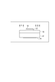
- FIG. 1 is a diagram showing an outline of the photon output device 1 of the present embodiment.
- the photon output device 1 of the present embodiment is a system that outputs photons, and includes a light emitting element 10, an optical element 20, and a current injection unit 30.
- the light-emitting element 10 is a semiconductor having a PIN structure including three layers of a p-type diamond layer 11, an n-type diamond layer 12, and an i-type diamond layer 13 provided between the p-type diamond layer 11 and the n-type diamond layer 12. including.
- the p-type diamond layer 11 is a semiconductor layer in which diamond is doped with a p-type dopant.
- the p-type diamond layer 11 is formed based on a diamond substrate to which about 10 20 boron (element symbol B) is added per cubic centimeter.
- the n-type diamond layer 12 is a semiconductor layer in which diamond is doped with an n-type dopant.
- the n-type diamond layer 12 has a thickness of about 500 nm, and about 10 18 phosphorus (element symbol P) is added per cubic centimeter.
- the i-type diamond layer 13 is an intrinsic semiconductor layer made of diamond that is almost non-doped and contains almost no p-type or n-type dopant.
- the i-type diamond layer 13 has a film thickness of about 10 ⁇ m, and the impurity concentration is suppressed to 0.1 ppb (parts per billion, parts per billion, 1 billionth) or less.
- a small amount of nitrogen (element symbol N) is intentionally ion-implanted from the main surface side (upper surface in FIG. 1) on the n-type diamond layer 12 side, and the ion-implanted nitrogen and vacancies are then combined. Annealed to let you.
- the main surface of the n-type diamond layer 12 is smaller than the main surface of the i-type diamond layer 13, and a part of the main surface of the i-type diamond layer 13 is exposed to the outside air. .
- the reason why a part of the main surface of the i-type diamond layer 13 is exposed to the outside air is that photons (arrow A in FIG. 1) generated from a predetermined position in the i-type diamond layer 13 are present. This is because, when outputting to the outside, the photons that have passed through the region exposed to the outside air are output to the outside, thereby making it easier to extract the photons.
- the predetermined position in the i-type diamond layer 13 is a nitrogen-vacancy complex defect center (hereinafter referred to as “NV center”) in which nitrogen and vacancies are adjacent at the molecular structure level. ) Is arbitrarily selected at the manufacturing stage.
- NV center existing immediately below any position in the region where the i-type diamond layer 13 is exposed to the outside air is selected as the predetermined position in the i-type diamond layer 13. .
- the reason why the impurity concentration in the i-type diamond layer 13 is suppressed to 0.1 ppb or less is that in order to see each photon generated from a single photon generation source one by one, adjacent single photon generation sources This is because it is considered necessary to make the interval of about 300 nm or more, and if the concentration is calculated by calculating backward from this, the impurity concentration becomes about 0.1 ppb. Therefore, in the i-type diamond layer 13, the average interval between the single photon generation sources is 300 nm or more apart, and it is possible to see one photon generated from the single photon generation source one by one.
- the main surface of the n-type diamond layer 12 is made smaller than the main surface of the i-type diamond layer 13 for ease of manufacturing, but not the n-type diamond layer 12 but the p-type diamond layer 11.
- the main surface may be smaller than the main surface of the i-type diamond layer 13.
- the main surface of at least one of the p-type diamond layer 11 and the n-type diamond layer 12 is made smaller than the main surface of the i-type diamond layer, and one of at least one main surface of the i-type diamond layer 13 is reduced. What is necessary is just to expose the area
- the PIN structure is stacked in the vertical direction with respect to the emission direction, and photons are output from the main surface of the i-type diamond layer 13 to the outside.
- the photons may be output to the outside from the cross section of the i-type diamond layer.
- the light-emitting element 10 further includes an electrode 14 formed on a part of the main surface of the p-type diamond layer 11 that is not in contact with the i-type diamond layer 13 (the surface below the p-type diamond layer 11 in FIG. 1). And an electrode 15 formed on the entire main surface of the n-type diamond layer 12 that is not in contact with the i-type diamond layer 13 (the upper surface of the n-type diamond layer 12 in FIG. 1).
- one electrode 14 and one electrode 15 are provided in one light-emitting element 10 in order to avoid an excessively complicated drawing, but the electrode 14 and / or the electrode 15 are A plurality may be provided as necessary.
- Each of the electrode 14 and the electrode 15 is a metal film provided for facilitating electrical connection by wire bonding or the like.
- the electrode 14 has a circular pattern with a radius of 400 ⁇ m
- the electrode 15 has a circular pattern with a radius of 200 ⁇ m.
- Each of the electrodes 14 has three layers of titanium 30 nm, platinum 30 nm, and gold 100 nm in order from the lower layer.
- the bottom layer is made of titanium because it has good contact properties with diamond, and platinum is laminated thereon to prevent oxidation of titanium. In order to improve the quality, gold is laminated. Note that the electrodes 14 and 15 are not necessarily required because they are provided to improve electrical reliability and facilitate processing.
- the optical element 20 allows photons generated at the predetermined position in the i-type diamond layer 13 to pass through.
- the photons emitted from the light emitting element 10 pass through the optical element 20 and are output to the outside of the photon output device 1.
- such an optical element 20 is also called an output unit.
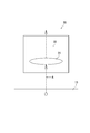
- FIG. 2 is a diagram showing an outline of an example of the optical element 20 in the present embodiment.
- the optical element 20 includes an objective lens 21 and a pinhole 22 disposed in the vicinity of the focal point of the objective lens 21, and uses the same principle as that of a confocal laser microscope, and the inside of the i-type diamond layer 13.
- the photons (arrow A in FIG. 2) emitted from a three-dimensional narrow region including the predetermined position are selectively output to the outside. For example, here, only a region having a circular field of view of about 350 nm and a depth direction of about 1 ⁇ m can be seen. Even if light enters from outside this region, what is the opening of the pinhole 22?
- the optical element 20 shown in FIG. 2 included the objective lens 21 and the pinhole 22, this Embodiment is not limited to this.
- the optical element 20 may include the objective lens 21 without including the pinhole.
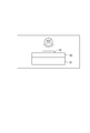
- FIG. 3 shows a schematic diagram of a configuration using an optical fiber 23 as the optical element 20.
- the optical fiber 23 has a core 23a and a clad 23b surrounding the core 23a. Photons generated at the emission center of the i-type diamond layer 13 propagate in the core 23a.
- connection method is particularly effective in outputting photons generated from a shallow point in the i-type diamond layer 13 that is relatively close to the outside air.
- the optical fiber 23 can control the range of the region where photons that can pass through the optical fiber 23 are generated by adjusting the diameter of the core 23 a and / or the distance between the i-type diamond layer 13 and the optical fiber 23.
- the optical element 20 faces the exposed part of the i-type diamond layer 13 without the p-type diamond layer 11 and the n-type diamond layer 12 interposed therebetween. For this reason, the optical element 20 allows photons generated at a predetermined position of the i-type diamond layer 13 to pass therethrough, and photons generated at another position of the i-type diamond layer 13, the p-type diamond layer 11 and the n-type diamond layer 12. Can be cut.
- the current injection unit 30 is a current source that applies a voltage between the electrode 14 and the electrode 15 and injects a current into the light emitting element 10.
- a current is appropriately injected at room temperature by the current injection unit 30, photons are generated from the predetermined position in the i-type diamond layer 13.
- the current injection unit 30 injects a forward current of about 1 to 20 mA into the light emitting element 10.
- the photon output device 1 of the present embodiment also includes the current injection unit 30 outside the own device, and the light emitting element 10 A configuration including the optical element 20 may be used.
- the photon output device of the comparative example has a light emitting element and a current injection part, but does not have an optical element. Although details are omitted, the light-emitting element in the photon output device of the comparative example includes a p-type diamond layer, an n-type diamond layer, and an i-type diamond layer provided between the p-type diamond layer and the n-type diamond layer. It has a PIN structure semiconductor composed of layers.
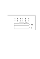
- FIG. 4A is a diagram showing light emission from the light emitting element in the photon output device of the comparative example
- FIG. 4B is a partially enlarged view of FIG.
- electrodes are provided at two locations, and it is understood from FIGS. 4A and 4B that light is emitted in the vicinity of the two electrodes.
- the i-type diamond layer emits light from the NV center, but the p-type diamond layer and the n-type diamond layer emit light using the doped impurity as the emission center.
- the concentration of the emission center of the p-type diamond layer and the n-type diamond layer is several orders of magnitude higher than the concentration of the emission center from the i-type diamond layer. Therefore, the light emitted from the light emitting element includes a light emitting component from the i-type diamond layer, and most of the light emitted from the light emitting element is emitted from the p-type diamond layer and the n-type diamond layer.
- the photon output device 1 of the present embodiment allows photons generated in the i-type diamond layer 13 of the light emitting element 10 to pass through the optical element 20, so that photons can be output to the outside with high spatial resolution. it can.
- ⁇ Manufacturing method> 5 to 12 are diagrams showing an outline of a method for manufacturing the light-emitting element 10.
- a method for manufacturing the light-emitting element 10 will be described in order with reference to FIGS.
- a p-type diamond substrate 101 as a base of the p-type diamond layer 11 is prepared and set in a CVD apparatus (Chemical Vapor Deposition system) 100.
- the p-type diamond substrate 101 finally becomes the p-type diamond layer 11 shown in FIG.
- a commercially available p-type diamond manufactured by TISNCM Research Institute in Russia
- HPHT High Pressure High Temperature Treatment
- the CVD apparatus 100 used in this embodiment is an ASTeX microwave plasma CVD apparatus sold by Seki Technotron Co., Ltd. in Japan, and has the same type of CVD apparatus or an equivalent function.
- methane gas (CH 4 ) and hydrogen gas (H 2 ) are supplied to the CVD reaction chamber using the CVD apparatus 100, and the i-type diamond 103 is formed by chemical vapor deposition.
- the thickness is controlled over the entire surface of the mold diamond substrate 101 to a thickness of about 10 ⁇ m.
- a CVD apparatus 100 is used to mix a small amount of phosphine (PH 3 ) with methane gas and hydrogen gas and supply them to the CVD reaction chamber.
- the diamond 102 is laminated on the entire surface of the i-type diamond 103 layer so as to have a thickness of about 500 nm.
- n-type diamond layer 12 shown in FIG. 1 is formed by removing the layer of the n-type diamond 102 around the circle having a diameter of 200 microns.
- the region of the i-type diamond 103 layer exposed to the outside air corresponds to a portion of the n-type diamond 102 layer that has been removed by dry etching.
- Nitrogen ions are implanted into the substrate.
- nitrogen is ion-implanted into the i-type diamond, vacancies can be formed together.
- about 10 to the 9th power of nitrogen per square centimeter is ion-implanted into the region exposed to the outside air at 180 keV.
- the ion implantation is not performed only in the region that is selectively exposed to the outside air, and the n-type diamond layer 12 is not particularly masked during the ion implantation.
- nitrogen is also ion-implanted into the n-type diamond layer 12.
- the amount of nitrogen implanted here is extremely small compared to the amount of dopant doped in the n-type diamond layer 12, the characteristics of the n-type diamond layer 12 are hardly changed even when nitrogen is ion-implanted. It is done.
- the position where the nitrogen ions are implanted the position where the NV center is formed can be arbitrarily arranged like a lattice.
- annealing is performed to combine nitrogen and vacancies. It is known that vacancies move at around 600 ° C. When nitrogen and vacancies are combined, a stable state is obtained. Therefore, if nitrogen is ion-implanted and then annealed at about 800 ° C. for about 1 hour, the vacancy moved and the nearby nitrogen and vacancies joined together to form an NV center. Here, for example, annealing is performed at 800 ° C. for about 2 hours to form the i-type diamond layer 13 shown in FIG.
- the electrode 15 is formed on the entire portion of the n-type diamond layer 12 exposed to the outside air, and the electrode is formed on a portion of the p-type diamond layer 11 exposed to the outside air. 14 is formed.
- unnecessary portions are masked by photolithography, and after only titanium, platinum, and gold are sequentially deposited on the necessary portions, the unnecessary portions of the mask are removed by photolithography to form the electrodes 14 and 15.
- annealing is performed in an argon gas at 420 ° C. for about 30 minutes in order to improve the characteristics of each electrode.
- the region exposed to the outside air is cleaned by irradiating hydrogen molecules with hydrogen atoms using a hot filament, and oxygen is further removed using plasma. Impurities such as organic substances on the surface are removed by irradiation with atoms and cleaning. Further, the surface of the region exposed to the outside air while suppressing damage to each electrode by cleaning the region exposed to the outside air stepwise by a plurality of different methods as described above. The impurities can be sufficiently removed.
- the light emitting element 10 generates photons by current injection from the current injection unit 30, but the present embodiment is not limited to this.
- the light emitting element 10 may generate photons by photoexcitation.
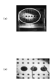
- FIG. 13A shows a confocal microscope fluorescence image of photons generated in the i-type diamond layer 13 by photoexcitation. Even when photoexcitation is performed, light emission from the i-type diamond layer 13 is observed through the optical element 20.
- FIG. 13B shows a confocal microscope fluorescence image of photons generated in the i-type diamond layer 13 by current injection. In either case, it is understood that a single photon is similarly output from the NV center.
- ⁇ Evaluation method> whether or not photons are output from a single photon generation source as intended from the light-emitting element 10 for both the case of photoexcitation using a YAG laser and the case of injecting a current.
- the evaluation will be based on academic proof called anti-bunching.
- Anti-bunching is indicated by an intensity correlation observed when the probability of detecting another individual photon in the vicinity of one photon detected by the photon correlation method is small.
- the NV center after one photon is emitted after excitation, the state returns from the excited state to the ground state. Therefore, another individual photon cannot be emitted until the state returns to the excited state again. The probability that a photon exists is reduced and anti-bunching is observed.
- FIG. 14 is a diagram showing an outline of an evaluation system when the operation of the light emitting element 10 in the present embodiment is evaluated.
- the light emitting element 10 is installed on the piezo stage 200, and the sample stage 200 (piezo stage) is finely moved in advance, and photons emitted from a three-dimensional narrow area including the position of the evaluation target. It adjusts so that only can be detected selectively.
- Laser light is output from the YAG laser generator 201, reflected by the dichroic mirror 202, the direction of travel is changed, passes through the objective lens 203, and is focused at a predetermined position in the light emitting element 10. tie.
- the light passing through the pinhole 204 is put into a beam splitter 205, and detected by two APDs (avalanche photodiodes) 206, respectively.
- the APD 206 is a photon counting module that outputs one TTL signal when one photon is detected.
- a signal output by detecting photons in the two APDs 206 is input to the personal computer 207 and processed.
- the personal computer 207 measures the time difference between the two signals output from the two APDs 206 and counts the time difference in the order of several ns to create a histogram.
- FIG. 15A is a graph showing the anti-bunching in the photon output device 1 of the present embodiment that emits light by photoexcitation
- FIG. 15B shows the anti-bunching in the photon output device 1 of the present embodiment that emits light by current injection. It is a graph which shows bunching.
- the dip at the time difference of zero was about 0.35.
- the dip at the time difference of zero was about 0.45.
- the emission intensity in the case of injecting current was comparable to that in the case of photoexcitation. Therefore, it was found that, in both cases of photoexcitation and current injection, photons are output from one single photon source in a three-dimensional narrow area adjusted in advance. . Therefore, it was verified that single photons generated from such a single photon generation source can be selectively output.
- light excitation when the distance between the NV centers in the i-type diamond layer 13 is short, photons generated from adjacent NV centers may not be distinguished from each other due to the limit of the wavelength of light.
- the current injection when a microfabricated electrode is used, even if the distance between the NV centers is relatively short, the photons generated from the adjacent NV centers can be distinguished by controlling the electrode for injecting the current. .
- single photons can be output from the i-type diamond layer by current injection at room temperature, so that single photons can be generated and output very efficiently. Can do. Therefore, it can be used for various devices that require a single photon in fields such as quantum cryptography communication and distributed processing quantum computers, and can greatly contribute to practical use.
- the present invention can be applied to various devices in fields such as quantum cryptography communication and distributed processing quantum computers. According to the present invention, a single photon can be efficiently generated and output without the need for a light source device or a cooling facility, and the cost of the apparatus can be greatly reduced without increasing the scale of the apparatus. Extremely expensive.
- Photon output device 10 Light emitting element 11 p-type diamond layer 12 n-type diamond layer 13 i-type diamond layer 14 Electrode 15 Electrode 20 Optical element 21 Objective lens 22 Pinhole 30 Current injection part
Landscapes
- Led Device Packages (AREA)
- Led Devices (AREA)
Abstract
本発明による光子出力装置は、p型ダイヤモンド層11、n型ダイヤモンド層12、及びp型ダイヤモンド層11とn型ダイヤモンド層12との間に積層されたi型ダイヤモンド層13からなるPIN構造の半導体を含む発光素子10と、i型ダイヤモンド層内において発生した光子を通過させる光学素子20とを備える。光学素子20は、i型ダイヤモンド層13の所定の位置において発生した光子を通過させ、i型ダイヤモンド層13の別の位置、p型ダイヤモンド層11およびn型ダイヤモンド層12において発生した光子をカットすることが好ましい。
Description
本発明は、光子出力装置に関し、特に、量子暗号通信等において利用される単一光子を、効率良く生成し出力するための技術に関する。
近年、デジタル通信による送金や電子商取引等の普及に伴い、通信される重要な情報を第三者による盗聴や改竄から守る、安全性を向上させる為の技術への要求が高まっている。安全性を向上させる為の有効な技術の1つに暗号(cryptography)がある。暗号方式には、主に公開鍵暗号方式と秘密鍵暗号方式とがある。これらの詳細は、池野信一、小山謙二著「現代暗号理論」(電子情報通信学会)に記載がある。公開鍵暗号方式では、送信側が公開鍵を保持し、公開鍵を用いて機密情報を暗号化し、受信側が秘密鍵を保持し、秘密鍵を用いて機密情報を復号する。
公開鍵暗号方式の公開鍵と秘密鍵とを更新するには、通常、受信側のそれぞれが公開鍵と秘密鍵との鍵ペアを生成して、公開鍵を送信側へ普通に送る。秘密鍵は送る必要がないので伝達時に第三者に知られる心配はなく、公開鍵は第三者に知られても機密情報が復号される事はないと考えられているので、鍵伝達時の機密管理が不要である。また公開鍵は保存時においても機密に管理する必要がないので、配信側の負担が小さい。
公開暗号鍵方式の安全性は、暗号化鍵から復号化鍵を生成することが容易でないという数学的な理論に基づいて担保されている。一般的に用いられているRSA暗号方式において暗号化鍵から復号化鍵を求めるためには、暗号化鍵である非常に大きな整数を素因数分解するという非常に難解な演算を行わなければならない。例えば最新のスーパーコンピュータを用いてこの演算を行ったとしても、非現実的な時間を要するため、暗号化鍵から復号化鍵を生成することは実質的に不可能であると考えられている。
しかしながら、大きな整数の素因数分解を比較的短時間で行うことができるような高性能なコンピュータが今後登場すれば、暗号化鍵から復号化鍵を生成することが可能になるので、将来的に公開暗号鍵方式は使用できなくなってしまうかもしれない。
一方、秘密鍵暗号方式では、送信側と受信側とが同一の共通鍵を秘密に保持し、送信側が共通鍵を用いて機密情報を暗号化し、受信側が共通鍵を用いて機密情報を復号する。秘密鍵暗号方式の共通鍵を更新するには、例えば送信側か受信側かのいずれか一方で新しい共通鍵を生成して、他方に新しい共通鍵を秘密に伝達しなければならない。新しい共通鍵が第三者に知られると機密情報が復号されて第三者に知られてしまうので、鍵伝達時の機密管理を徹底しなければならない。
なお安全対策上、暗号化や復号に用いる鍵は、定期的、或いは必要に応じて頻繁に更新することが望ましい。また暗号化前の機密情報と長さが同じ秘密鍵を1回で使い捨てるVernam暗号という暗号方式は、理論的に絶対に安全であることが理論的に証明されている。
そこで、この共通鍵を秘密に伝達する手段として、量子暗号通信に対する期待が高まっている。量子暗号通信では、単一光子の量子状態の1つに情報を与え、単一光子を伝送媒体として伝送する。光子の量子状態には、光子の偏光(光の波の向き)、位相、スピンなどの様々な種類がある。
観測者が単一光子の量子状態の1つを測定すると必ず他の量子状態に影響を及ぼすという量子力学的な原理があるので、量子暗号通信において第三者によって盗聴が行われた場合には、盗聴が行われた可能性がある事を、正規の通信者達が知ることができると考えられている。よって盗聴が行われた可能性があるときには伝達された共通鍵を破棄し、盗聴が行われた可能性がないときに伝達された共通鍵のみを用いて暗号化通信を行えば、通信の安全性が確保される。
以下に量子暗号通信の原理の概要について説明する。
まず送信者は、1ビットの情報を送ろうとする度に、Aという種類の量子状態を用いて送信するかBという種類の量子状態を用いて送信するかをランダムに決め、選択した種類の量子状態が、送ろうとする1ビットの情報に対応する状態である単一光子を送信する。このとき同一の単一光子において、選択しなかった方の種類の量子状態は、量子力学的な原理により不確定であり、どういう状態なのかを量子状態を変えずに知ることができない。
受信者は、送られてきた単一光子について、Aという種類の量子状態を測定するかBという種類の量子状態を測定するかをランダムに決め、選択した種類の量子状態を測定して1ビットの情報を得る。このとき選択した種類の量子状態を測定すると、他の量子状態が変わってしまうので、選択しなかった方の種類の量子状態を正しく知ることはできない。
その後、送信者と受信者とが同じ選択をしたか否かの答え合わせを行い、同じ選択をした場合には得られた情報を有効な情報として保持し、同じ選択をしていなかった場合には得られた情報を破棄する。このような1ビット毎の通信を繰り返すことで、所定量の情報の通信を行うことができる。ここで、盗聴者がいない場合には情報は正しく通信される。
ところが、盗聴者がいる場合には、盗聴者が盗聴することにより単一光子の量子状態が変化して、一定確率で情報に間違いが生じる。
盗聴者は盗聴する時点で、送信者が選択した量子状態の種類を知ることができないので、受信者と同様にAという種類の量子状態を測定するかBという種類の量子状態を測定するかをランダムに決め、選択した種類の量子状態を測定して1ビットの情報を得ることになる。ここで、たまたま盗聴者が送信者と同じ選択をした場合には、盗聴者は正しい情報を得ることができ、かつ、選択した種類の量子状態を同じ状態にした単一光子を送信し直せば、盗聴していることを正規の通信者達に知られることはない。
ところが、偶然に送信者と同じ選択をし続けることは到底不可能であり、通常50%の確率で受信者と異なる選択をすることになる。盗聴者が受信者と異なる選択をした場合には、異なる選択をした50%のうちのさらに50%(合わせて25%)が間違った情報となる。ここで、単一光子を送信し直しても、50%の確率で、間違った情報に対応する状態である単一光子を送信してしまう。このような単一光子は、さらに受信者が送信者と同じ選択をした場合に間違った情報を受信者に与えることになる。従って、盗聴者は、送信者が送ろうとした情報を全部盗聴しても、そのうちの25%は間違った情報である上に、盗聴することによって、正規の受信者が受信する情報のうちの25%を間違った情報に変えてしまう。
よって、送信者と受信者とが、所定量の情報の通信を行った後に、ランダムにいくつかのビットを抜き出して、正しい情報が送信されているか否かを確認すれば、100%正しいと確認された場合には盗聴が行われた可能性がないとわかるので、安心してこのときに受信した情報を共通鍵として用いることができる。
ここで量子暗号通信には、単一光子を繰り返し出力することができる光子出力装置が不可欠である。例えば、従来の単一光子を生成させる方法としては、量子ドットに短波長の光を照射する光励起による第1の方法(例えば、特許文献1)や、半導体のp-n接合を利用して量子ドットに電気的に電荷を注入し、電子と正孔を再結合させることによって単一光子を発生させる第2の方法(例えば、特許文献2)等がある。また、本願の発明と関連が深い発光素子に関する技術が特許文献3に開示されている。
しかしながら、上記第1の方法では、高品質の単一光子を発生させるために励起パルス光の波長を正確に調整しなければならないので、高価な光源装置が必要であり装置規模が大きくなりコストが高くなる。
また上記第2の方法では、不必要な波長の発光が混在するなどの不具合が発生しやすく、高品質の単一光子を得ることが難しい。また電気的に電荷を注入による方法では、本願の発明者が知る限り室温で動作した例がなく、別途冷却設備が必要であり、第1の方法と同様に装置規模が大きくなりコストが高くなる。
以上のように、単一光子を効率良く生成するための技術は未だ確立しておらず、新しい技術の開発が望まれている。そこで、本発明は、光源装置や冷却設備を必要とせず、単一光子を効率良く生成し出力することができる光子出力装置、光子出力方法、及び光子出力装置に用いる半導体の製造方法を提供することを目的とする。
本発明による光子出力装置は、p型ダイヤモンド層、n型ダイヤモンド層、及び、前記p型ダイヤモンド層と前記n型ダイヤモンド層との間に設けられたi型ダイヤモンド層からなるPIN構造の半導体を含む発光素子と、前記i型ダイヤモンド層内において発生した光子を通過させる光学素子とを備える。
ある実施形態において、前記光学素子は、前記i型ダイヤモンド層の所定の位置において発生した光子を通過させ、前記i型ダイヤモンド層の別の位置、前記p型ダイヤモンド層および前記n型ダイヤモンド層において発生した光子をカットする。
ある実施形態において、前記光子出力装置は、前記PIN構造の半導体に電圧を印加して、前記発光素子に電流を注入する電流注入部をさらに備える。
ある実施形態において、前記i型ダイヤモンド層内に、窒素と空孔とが隣接する窒素-空孔複合体欠陥中心が形成されている。
ある実施形態において、前記i型ダイヤモンド層内に、窒素がイオン注入されている。
ある実施形態において、前記光学素子は、対物レンズと、当該対物レンズの焦点付近に配置されたピンホールとを含む。
ある実施形態において、前記光学素子は、外部へ単一光子を出力する。
ある実施形態において、前記i型ダイヤモンド層における不純物の濃度は0.1ppb以下である。
ある実施形態において、前記i型ダイヤモンド層の主面は、前記p型ダイヤモンド層、及び、前記n型ダイヤモンド層のうちの少なくとも一方の層の主面よりも小さく、前記i型ダイヤモンド層の主面には、外気に対して露出している領域があり、前記光学素子は、前記外気に対して露出している領域内を通過した光子を外部へ出力する。
ある実施形態において、前記i型ダイヤモンド層の前記外気に対して露出している領域がクリーニングされている。
ある実施形態では、前記発光素子において、前記p型ダイヤモンド層となる材料基板の表面に、前記i型ダイヤモンド層が積層され、前記i型ダイヤモンド層の上の一部に前記n型ダイヤモンド層が積層され、前記n型ダイヤモンド層の上に電極が形成されており、前記外気に対して露出している領域は、前記i型ダイヤモンド層の上に前記n型ダイヤモンド層が積層されていない部分に相当し、当該外気に対して露出している領域が、前記電極の形成後に、異なる複数の方法で段階的にクリーニングされている。
ある実施形態において、前記光子出力装置は、室温において動作する。
本発明による光子出力方法は、p型ダイヤモンド層、n型ダイヤモンド層、及び、前記p型ダイヤモンド層と前記n型ダイヤモンド層との間に積層されたi型ダイヤモンド層からなるPIN構造の半導体を含む発光素子を用意する用意ステップと、前記発光素子を発光させる発光ステップと、前記発光ステップにて前記i型ダイヤモンド層内において発生した光子を光学素子に通過させる光子通過ステップとを包含する。
ある実施形態において、前記発光ステップは、前記PIN構造の半導体に電圧を印加して、前記発光素子に電流を注入するステップを含む。
本発明による半導体の製造方法は、p型ダイヤモンド層、n型ダイヤモンド層、及び、前記p型ダイヤモンド層と前記n型ダイヤモンド層との間に積層されたi型ダイヤモンド層からなるPIN構造の半導体の製造方法であって、前記i型ダイヤモンド層内に窒素をイオン注入する注入ステップを含む。
本発明によれば、発光素子をPIN構造の半導体にすることで、半導体の特性を生かして電流注入を容易に行うことができるのと同時に、非常に光るものを少なくしたようなきれいな膜であるi型ダイヤモンド層からの発光を見るような仕組みにすることによって、1個の不純物等から発生する光子のみを比較的容易に出力することができるという優れた効果を有する。
(実施の形態)
<概要>
実施の形態は、PIN構造の半導体の特性を生かして電流を注入することにより、世界で初めて、室温において、電流注入によりi型ダイヤモンド層から単一光子を出力させることを可能にした光子出力装置である。
<概要>
実施の形態は、PIN構造の半導体の特性を生かして電流を注入することにより、世界で初めて、室温において、電流注入によりi型ダイヤモンド層から単一光子を出力させることを可能にした光子出力装置である。
<構成>
図1は、本実施の形態の光子出力装置1の概要を示す図である。図1に示すように、本実施の形態の光子出力装置1は、光子を出力するシステムであり、発光素子10、光学素子20、及び電流注入部30を備える。発光素子10は、p型ダイヤモンド層11、n型ダイヤモンド層12、及びp型ダイヤモンド層11とn型ダイヤモンド層12との間に設けられたi型ダイヤモンド層13の3層からなるPIN構造の半導体を含む。
図1は、本実施の形態の光子出力装置1の概要を示す図である。図1に示すように、本実施の形態の光子出力装置1は、光子を出力するシステムであり、発光素子10、光学素子20、及び電流注入部30を備える。発光素子10は、p型ダイヤモンド層11、n型ダイヤモンド層12、及びp型ダイヤモンド層11とn型ダイヤモンド層12との間に設けられたi型ダイヤモンド層13の3層からなるPIN構造の半導体を含む。
p型ダイヤモンド層11は、ダイヤモンドにp型のドーパントがドープされた半導体層である。例えば、p型ダイヤモンド層11は、1立法センチあたり10の20乗個程度のほう素(元素記号B)が添加されたダイヤモンド基板を元に形成される。
n型ダイヤモンド層12は、ダイヤモンドにn型のドーパントがドープされた半導体層である。例えばn型ダイヤモンド層12は、膜厚が500nm程度であり、1立法センチあたり10の18乗個程度のリン(元素記号P)が添加されている。
i型ダイヤモンド層13は、p型やn型のドーパントをほとんど含有していないほぼノンドープの状態であるダイヤモンドからなる真性半導体層である。例えば、i型ダイヤモンド層13は、膜厚が10μm程度であり、不純物の濃度が0.1ppb(パーツ・パー・ビリオン、parts per billion、10億分の1)以下に抑えられている。また微量の窒素(元素記号N)が意図的に、n型ダイヤモンド層12側の主面側(図1における上側の面)からイオン注入され、その後にイオン注入された窒素と空孔とを結合させるためにアニーリングされている。
また本実施の形態では、n型ダイヤモンド層12の主面がi型ダイヤモンド層13の主面よりも小さく、i型ダイヤモンド層13の主面の一部の領域が外気に対して露出している。このようにi型ダイヤモンド層13の主面の一部の領域が外気に対して露出している理由は、i型ダイヤモンド層13内の所定の位置から発生する光子(図1中矢印A)を外部へ出力する際に、この外気に対して露出している領域内を通過した光子を外部へ出力することにより、光子を取り出し易くするためである。
ここで、i型ダイヤモンド層13内の上記所定の位置とは、窒素と空孔とが分子構造レベルで隣接する、窒素‐空孔複合体欠陥中心(nitrogen vacancy center、以下「NV中心」と記す)が形成されているいくつかの地点の1つを、製造段階で任意に選択したものである。本実施の形態では、i型ダイヤモンド層13が外気に対して露出した領域内の何れかの位置の直下に存在するNV中心を、i型ダイヤモンド層13内の上記所定の位置として選択している。
ここでi型ダイヤモンド層13における不純物の濃度を0.1ppb以下に抑えている理由は、単一光子発生源から発生する光子を1個1個見るためには、隣り合う単一光子発生源同士の間隔を300nm程度以上にする必要があると考えられるので、これから逆算をして濃度を出すと、不純物の濃度が0.1ppb程度になるからである。従って、i型ダイヤモンド層13では単一光子発生源同士の間隔の平均が300nm以上離れており、単一光子発生源から発生する光子を1個1個見ることが可能な状態になっている。
ちなみに、半導体中の不純物の濃度を0.1ppb以下にすることが可能なのは、現在の技術ではシリコンとダイヤモンドくらいしかなく、化合物半導体では不可能である。また、p型ダイヤモンド層11、及びダイヤモンド層12では、i型ダイヤモンド層13に比べると不純物の濃度が桁違いに高いので高い濃度で様々な発光中心が存在し、いたる所が光っているような状態になっており、i型ダイヤモンド層13のように単一光子発生源から発生する光子を1個1個見ることは不可能だと思われる。
なお、本実施の形態では、製造の容易さからn型ダイヤモンド層12の主面をi型ダイヤモンド層13の主面よりも小さくしているが、n型ダイヤモンド層12ではなくp型ダイヤモンド層11の主面をi型ダイヤモンド層13の主面よりも小さくしてもよい。要は、p型ダイヤモンド層11とn型ダイヤモンド層12のうちの少なくとも一方の層の主面をi型ダイヤモンド層の主面よりも小さくし、i型ダイヤモンド層13の少なくとも一方の主面の一部の領域を、外気に対して露出させればよい。
また、本実施の形態ではPIN構造を出射方向に対して縦方向に積んで、i型ダイヤモンド層13の主面から光子を外部へ出力しているが、PIN構造を出射方向に対して横方向に積んで、i型ダイヤモンド層の断面から光子を外部へ出力してもよい。
発光素子10は、さらに、p型ダイヤモンド層11におけるi型ダイヤモンド層13と接していない側の主面(図1におけるp型ダイヤモンド層11の下側の面)の一部に形成された電極14と、n型ダイヤモンド層12におけるi型ダイヤモンド層13と接していない側の主面(図1におけるn型ダイヤモンド層12の上側の面)の全面に形成された電極15を含む。なお、図1では、図面が過度に複雑になることを避けるために、1つの発光素子10に、電極14および電極15が1つずつ設けられているが、電極14および/または電極15は、必要に応じて複数設けられてもよい。
電極14、及び電極15はそれぞれ、ワイヤーボンディング等により電気的に接続することを容易にするために設けられた金属皮膜であり、電極14と電極15との間に電圧を印加すれば、発光素子10におけるPIN構造の半導体に電圧を印加することができる。例えば、電極14は半径400μmの円形パターンであり、電極15は半径200μmの円形パターンであり、それぞれ下層から順に、チタン30nm、白金30nm、及び金100nmの3層からなる。
ここで電極14、及び電極15において、最下層をチタンにしたのはダイヤモンドとのコンタクト性がよいからであり、この上にチタンの酸化を防止するために白金を積層し、さらに、ワイヤーボンディング性をよくするために金を積層している。なお、電極14、及び電極15は、電気的な信頼性を向上させるため、及び加工を容易にするために設けられたものであるので、必ずしも必要な構成ではない。
また、発光素子10の製造方法については別途下記に記載する。
光学素子20は、i型ダイヤモンド層13内の上記所定の位置において発生した光子を通過させる。このように、発光素子10から出た光子は光学素子20を通過して光子出力装置1の外部に出力される。このため、このような光学素子20は出力部とも呼ばれる。
図2は、本実施の形態における光学素子20の一例の概略を示す図である。図2に示すように光学素子20は、対物レンズ21、及び対物レンズ21の焦点付近に配置されたピンホール22を含み、共焦点レーザ顕微鏡と同様の原理を用いて、i型ダイヤモンド層13内の上記所定の位置を含む3次元的に狭小な領域から発せられる光子(図2中矢印A)を、選択的に外部へ出力するように調整されている。例えば、ここでは、視野方向が350nmくらいの円状、かつ深さ方向が1μmくらいの領域しか見えないようにしており、この領域外から光が入ったとしても、ピンホール22の開口部分とは違う位置に焦点を結ぶので、ピンホール22に遮られて排除され、この領域から発せられた光しか通過しない。このため、i型ダイヤモンド層13の特定の領域において発生した光子を高い分解能で外部に出力させることができる。
なお、図2に示した光学素子20は、対物レンズ21及びピンホール22を含んでいたが、本実施の形態はこれに限定されない。i型ダイヤモンド層13内のNV中心間の間隔が比較的大きい場合、光学素子20はピンホールを含むことなく、対物レンズ21を含んでいてもよい。
あるいは、対物レンズ21、及びピンホール22の代わりに、伝送用の光ファイバーを、i型ダイヤモンド層13内の上記所定の位置に最も近いi型ダイヤモンド層13の表面に光学的に直接接続してもよい。図3に、光学素子20として光ファイバー23を用いた構成の概略図を示す。光ファイバー23は、コア23aと、コア23aを囲むクラッド23bとを有している。i型ダイヤモンド層13の発光中心において発生した光子はコア23a内を伝搬する。
なおこのような接続方法は、i型ダイヤモンド層13内の比較的外気に近い浅い地点から発生する光子を出力させる場合に特に有効である。光ファイバー23は、コア23aの径および/またはi型ダイヤモンド層13と光ファイバー23との距離を調整することにより、光ファイバー23を通過可能な光子の発生する領域の範囲を制御することができる。
このように、光学素子20は、p型ダイヤモンド層11およびn型ダイヤモンド層12を介することなくi型ダイヤモンド層13の露出した部分と対向している。このため、光学素子20は、i型ダイヤモンド層13の所定の位置において発生した光子を通過させ、i型ダイヤモンド層13の別の位置、p型ダイヤモンド層11およびn型ダイヤモンド層12において発生した光子をカットできる。
電流注入部30は、電極14と電極15との間に電圧を印加して、発光素子10に電流を注入する電流源である。電流注入部30により、室温において適宜電流が注入されることにより、i型ダイヤモンド層13内の上記所定の位置から光子が発生する。例えば電流注入部30は、発光素子10に1~20mA程度の順電流を注入する。
なお、他の一般の装置において電源部分を自装置外に備えることは珍しくないので、本実施の形態の光子出力装置1においても電流注入部30を自装置外に備えることとし、発光素子10と光学素子20からなる構成にしてもよい。
ここで、比較例の光子出力装置と比較して本実施の形態における光子出力装置1の利点を説明する。比較例の光子出力装置は発光素子および電流注入部を有しているものの、光学素子を有していない。詳細を省略するが、比較例の光子出力装置における発光素子は、p型ダイヤモンド層、n型ダイヤモンド層、及びp型ダイヤモンド層とn型ダイヤモンド層との間に設けられたi型ダイヤモンド層の3層からなるPIN構造の半導体を有している。
以下に、図4を参照して、比較例の光子出力装置における発光素子からの発光を説明する。図4(a)は比較例の光子出力装置における発光素子からの発光を示す図であり、図4(b)は図4(a)の一部拡大図である。この光子出力装置では、2箇所に電極が設けられており、図4(a)および図4(b)から、2つの電極の近傍において発光していることが理解される。
上述したように、i型ダイヤモンド層ではNV中心から発光するが、p型ダイヤモンド層およびn型ダイヤモンド層ではドープされている不純物を発光中心として発光する。このため、p型ダイヤモンド層およびn型ダイヤモンド層の発光中心の濃度はi型ダイヤモンド層からの発光中心の濃度よりも数桁以上多い。したがって、発光素子からの発光はi型ダイヤモンド層からの発光成分を含んでいるが、この発光のほとんどの成分がp型ダイヤモンド層およびn型ダイヤモンド層からの発光である。これに対して、本実施の形態の光子出力装置1は、発光素子10のi型ダイヤモンド層13において発生した光子を光学素子20に通過させるため、高い空間分解能で光子を外部に出力させることができる。
<製造方法>
図5~図12は、発光素子10の製造方法の概略を示す図である。以下に図5~図12を用いて、発光素子10の製造方法について、順を追って説明する。
図5~図12は、発光素子10の製造方法の概略を示す図である。以下に図5~図12を用いて、発光素子10の製造方法について、順を追って説明する。
(1)図5に示すように、p型ダイヤモンド層11の元になるp型ダイヤモンド基板101を準備して、CVD装置(Chemical Vapor Deposition system)100にセットする。p型ダイヤモンド基板101は、最終的に図1に示したp型ダイヤモンド層11になる。
本実施の形態では、高温高圧法(HPHT:High Pressure High Temperature Treatment)により合成された、一般に販売されているp型ダイヤモンド(ロシアのTISNCM研究所製)を購入してこれを使用した。また本実施の形態で用いたCVD装置100は、日本のセキテクノトロン株式会社から販売されているASTeX(アステックス)社製のマイクロ波プラズマCVD装置であり、同型のCVD装置、又は同等の機能を持つ他のCVD装置を購入して、本実施の形態と同様の特性になるように調整するか、あるいは同様の条件を用いれば、誰でも発光素子10を製造することが可能である。
(2)図6に示すように、CVD装置100を用いて、メタンガス(CH4)と水素ガス(H2)とをCVD反応室に供給し、化学気相堆積によってi型ダイヤモンド103を、p型ダイヤモンド基板101の表面全体に厚さを管理して10μm程度まで積層する。
(3)図7に示すように、CVD装置100を用いて、メタンガスと水素ガスに、さらに微量のホスフィン(phosphine、PH3)を混ぜてCVD反応室に供給し、化学気相堆積によってn型ダイヤモンド102を、i型ダイヤモンド103の層の表面全体に厚さを管理して500nm程度まで積層する。
(4)図8に示すように、n型ダイヤモンド102を積層したものをCVD装置100から取り出し、n型ダイヤモンド102の層の一部を酸素ガスによるドライエッチングで抜いて、i型ダイヤモンド103の層の一部の領域を外気に対して露出させる。本実施の形態では、200ミクロンの直径の円を残して、その周りのn型ダイヤモンド102の層を除去して、図1に示したn型ダイヤモンド層12が形成される。
(5)図9に示すように、i型ダイヤモンド103の層の外気に対して露出している領域は、n型ダイヤモンド102の層の一部をドライエッチングで抜いた部分に相当し、この領域に窒素をイオン注入する。ここでi型ダイヤモンドに窒素をイオン注入すると、付随して空孔もいっしょにできる。例えばこの外気に対して露出している領域に、1平方センチあたり10の9乗個程度の窒素を180keVでイオン注入する。
なお、ここでは、選択的に上記外気に対して露出している領域だけにイオン注入しているわけではなく、イオン注入に際して特にn型ダイヤモンド層12にマスクをかけるようなことはしていないので、n型ダイヤモンド層12にも同時に窒素がイオン注入されてしまう。しかしながら、ここで注入する窒素の量はn型ダイヤモンド層12にドープしたドーパントの量に比べて極めて微量なので、n型ダイヤモンド層12の特性は窒素がイオン注入されてもほとんど変わることはないと考えられる。また、窒素をイオン注入する位置を空間的に制御することにより、NV中心が形成される位置を格子状等のように任意に配置することも可能である。
(6)図10に示すように、窒素と空孔とを結合させるためにアニーリングする。空孔は600℃くらいで動くということが知られている。また窒素と空孔とが結合すると安定した状態になる。そこで窒素をイオン注入した後に、800℃くらいで1時間程度アニーリングすると、空孔が動いてたまたま近くにあった窒素と空孔とがくっついてNV中心ができる。ここでは例えば、800℃で2時間程度アニーリングし、図1に示したi型ダイヤモンド層13が形成される。
(7)図11に示すように、n型ダイヤモンド層12の外気に対して露出した部分の全体に電極15を形成し、p型ダイヤモンド層11の外気に対して露出した部分の一部に電極14を形成する。ここでは、フォトリソで不要部分はマスクをし、必要部分だけにチタン、白金、金を順に全体に蒸着した後で、フォトリソで不要な部分のマスクを取り除くことにより、電極14と電極15とを形成する。またここでは、電極14と電極15とを形成した後に、各電極の特性を向上させるためにアルゴンガス中で420℃、30分程度アニーリングする。
(8)図12に示すように、上記外気に対して露出している領域に対して、熱フィラメントを用いて水素分子を水素原子にして照射してクリーニングし、さらに、プラズマを用いて酸素を原子にして照射してクリーニングすることにより、表面の有機物等の不純物を除去する。また上記外気に対して露出している領域を、このように異なる複数の方法により、段階的にクリーニングすることにより、各電極への損傷を抑えながら上記外気に対して露出している領域の表面の不純物を十分に除去することができる。
なお、図1に示した子出力装置1では、発光素子10は電流注入部30からの電流注入によって光子を発生したが、本実施の形態はこれに限定されない。発光素子10は光励起によって光子を発生してもよい。
図13(a)は、光励起によってi型ダイヤモンド層13内において発生した光子の共焦点顕微鏡蛍光像を示す図である。光励起をした場合でもi型ダイヤモンド層13からの発光は光学素子20を介して観察される。図13(b)は、電流注入によってi型ダイヤモンド層13内において発生した光子の共焦点顕微鏡蛍光像を示す図である。いずれの場合でも、NV中心から単一光子が同様に出力されていることが理解される。
<評価方法>
ここでは、YAGレーザを用いて光励起させる場合と、電流を注入する場合の両方について、発光素子10から、意図した通りに1個の単一光子発生源から光子が出力されているか否かを、アンチバンチングと言われている学術的な証明を用いて評価することとする。アンチバンチングは、光子相関法による測定で、1個の光子を検出したときにその近くにもう1個別の光子を検出する確率が小さくなっている場合に観測される強度相関から示される。NV中心の場合、励起後に光子を1個放出した後は励起状態から基底状態に戻ってしまうので、再び励起状態に戻るまではもう1個別の光子を放出できず、時間的に近接した2つの光子の存在する確率が小さくなり、アンチバンチングが観測される。
ここでは、YAGレーザを用いて光励起させる場合と、電流を注入する場合の両方について、発光素子10から、意図した通りに1個の単一光子発生源から光子が出力されているか否かを、アンチバンチングと言われている学術的な証明を用いて評価することとする。アンチバンチングは、光子相関法による測定で、1個の光子を検出したときにその近くにもう1個別の光子を検出する確率が小さくなっている場合に観測される強度相関から示される。NV中心の場合、励起後に光子を1個放出した後は励起状態から基底状態に戻ってしまうので、再び励起状態に戻るまではもう1個別の光子を放出できず、時間的に近接した2つの光子の存在する確率が小さくなり、アンチバンチングが観測される。
図14は、本実施の形態における発光素子10の動作を評価した際の評価システムの概略を示す図である。図14に示す評価システムにおいて、ピエゾステージ200に発光素子10が設置され、予め試料台200(ピエゾステージ)を微細に動かして、評価対象の位置を含む3次元的に狭小な領域から発せられる光子のみを選択的に検出することができるように調整しておく。
・光励起させる場合
(1)YAGレーザ発生装置201からレーザ光が出力され、ダイクロイックミラー202によって反射して進行方向が変えられ、対物レンズ203を通って、発光素子10内の所定の位置で焦点を結ぶ。
(1)YAGレーザ発生装置201からレーザ光が出力され、ダイクロイックミラー202によって反射して進行方向が変えられ、対物レンズ203を通って、発光素子10内の所定の位置で焦点を結ぶ。
(2)ここで発光した光は、レーザ光とはエネルギーが異なり波長が違うため、対物レンズ203で集光されてダイクロイックミラー202を通過し、ピンホール204によって狭小な領域から発せられるもののみが選択的に通過する。
(3)ピンホール204を通過した光をビームスプリッタ205に入れて分け、2台のAPD(アバランシェフォトダイオード)206においてそれぞれ検出する。ここでAPD206は1個フォトンを検出すると、1個のTTL信号を出すフォトンカウンティングモジュールである。
(4)2台のAPD206において光子が検出されることにより出力された信号は、パソコン207に入力されて処理される。パソコン207は2台のAPD206よりそれぞれ出力された2つの信号の時間差を計り、数ns程度のオーダーで時間差ごとにカウントしてヒストグラムを作る。
(5)時間差ごとのカウントしたヒストグラムを、縦軸が0から1までのスケールになるようにノーマライズし、時間差ゼロのところのディップが0.5より小さいか否かを判定する。時間差ゼロのところのディップが0.5より小さければ、1個の単一光子発生源から光子が出力されていることの証明になる。
・電流を注入する場合
(1)電流注入部30を用いて、電極14と電極15との間に電圧を印加して、発光素子10に電流を注入する。
・電流を注入する場合
(1)電流注入部30を用いて、電極14と電極15との間に電圧を印加して、発光素子10に電流を注入する。
(2)~(5)光励起させる場合の(2)~(5)と同様である。
<評価結果>
図15(a)は光励起で発光した本実施の形態の光子出力装置1におけるアンチバンチングを示すグラフであり、図15(b)は電流注入で発光した本実施の形態の光子出力装置1におけるアンチバンチングを示すグラフである。光励起させる場合においては、時間差ゼロのところのディップはおよそ0.35であった。電流を注入する場合においては、時間差ゼロのところのディップはおよそ0.45であった。
図15(a)は光励起で発光した本実施の形態の光子出力装置1におけるアンチバンチングを示すグラフであり、図15(b)は電流注入で発光した本実施の形態の光子出力装置1におけるアンチバンチングを示すグラフである。光励起させる場合においては、時間差ゼロのところのディップはおよそ0.35であった。電流を注入する場合においては、時間差ゼロのところのディップはおよそ0.45であった。
また、電流を注入する場合の発光強度は、光励起の場合と遜色ないものであった。よって、光励起させる場合、及び電流を注入する場合のいずれの場合でも、予め調整した3次元的に狭小な領域において、1個の単一光子発生源から光子が出力されているという事がわかった。よって、このような単一光子発生源から発生する単一光子を選択的に出力することが可能である事が検証された。なお、光励起では、i型ダイヤモンド層13内のNV中心間距離が短い場合、光の波長の限界から、隣接するNV中心から発生した光子を区別できないことがある。これに対して、電流注入では、微細加工した電極を用いると、NV中心間距離が比較的短くても、電流を注入する電極を制御することにより、隣接するNV中心から発生した光子を区別できる。
<まとめ>
以上に説明したように、本実施の形態によれば、室温において、電流注入によりi型ダイヤモンド層から単一光子を出力させることができるので、非常に効率良く単一光子を生成し出力することができる。よって、量子暗号通信や分散処理型量子コンピュータなどの分野における単一光子を必要とする様々な装置の利用に供し、実用化に大きく貢献することができる。
以上に説明したように、本実施の形態によれば、室温において、電流注入によりi型ダイヤモンド層から単一光子を出力させることができるので、非常に効率良く単一光子を生成し出力することができる。よって、量子暗号通信や分散処理型量子コンピュータなどの分野における単一光子を必要とする様々な装置の利用に供し、実用化に大きく貢献することができる。
本発明は、量子暗号通信や分散処理型量子コンピュータなどの分野における様々な装置に適用することができる。本発明によって、光源装置や冷却設備を必要とせずに単一光子を効率良く生成し出力することができ、装置規模が大きくならずコストを大幅に抑えることができるので、その産業的利用価値は極めて高い。
1 光子出力装置
10 発光素子
11 p型ダイヤモンド層
12 n型ダイヤモンド層
13 i型ダイヤモンド層
14 電極
15 電極
20 光学素子
21 対物レンズ
22 ピンホール
30 電流注入部
10 発光素子
11 p型ダイヤモンド層
12 n型ダイヤモンド層
13 i型ダイヤモンド層
14 電極
15 電極
20 光学素子
21 対物レンズ
22 ピンホール
30 電流注入部
Claims (15)
- p型ダイヤモンド層、n型ダイヤモンド層、及び、前記p型ダイヤモンド層と前記n型ダイヤモンド層との間に設けられたi型ダイヤモンド層からなるPIN構造の半導体を含む発光素子と、
前記i型ダイヤモンド層内において発生した光子を通過させる光学素子と
を備える、光子出力装置。 - 前記光学素子は、前記i型ダイヤモンド層の所定の位置において発生した光子を通過させ、前記i型ダイヤモンド層の別の位置、前記p型ダイヤモンド層および前記n型ダイヤモンド層において発生した光子をカットする、請求項1に記載の光子出力装置。
- 前記光子出力装置は、前記PIN構造の半導体に電圧を印加して、前記発光素子に電流を注入する電流注入部をさらに備える、請求項1または2に記載の光子出力装置。
- 前記i型ダイヤモンド層内に、窒素と空孔とが隣接する窒素-空孔複合体欠陥中心が形成されている、請求項1から3のいずれかに記載の光子出力装置。
- 前記i型ダイヤモンド層内に、窒素がイオン注入されている、請求項4に記載の光子出力装置。
- 前記光学素子は、対物レンズと、当該対物レンズの焦点付近に配置されたピンホールとを含む、請求項1から5のいずれかに記載の光子出力装置。
- 前記光学素子は、外部へ単一光子を出力する、請求項1から6のいずれかに記載の光子出力装置。
- 前記i型ダイヤモンド層における不純物の濃度は0.1ppb以下である、請求項7に記載の光子出力装置。
- 前記i型ダイヤモンド層の主面は、前記p型ダイヤモンド層、及び、前記n型ダイヤモンド層のうちの少なくとも一方の層の主面よりも小さく、
前記i型ダイヤモンド層の主面には、外気に対して露出している領域があり、
前記光学素子は、前記外気に対して露出している領域内を通過した光子を外部へ出力する、請求項1から8のいずれかに記載の光子出力装置。 - 前記i型ダイヤモンド層の前記外気に対して露出している領域がクリーニングされている、請求項9に記載の光子出力装置。
- 前記発光素子において、
前記p型ダイヤモンド層となる材料基板の表面に、前記i型ダイヤモンド層が積層され、
前記i型ダイヤモンド層の上の一部に前記n型ダイヤモンド層が積層され、
前記n型ダイヤモンド層の上に電極が形成されており、
前記外気に対して露出している領域は、前記i型ダイヤモンド層の上に前記n型ダイヤモンド層が積層されていない部分に相当し、当該外気に対して露出している領域が、前記電極の形成後に、異なる複数の方法で段階的にクリーニングされている、請求項10に記載の光子出力装置。 - 前記光子出力装置は、室温において動作する請求項1から11のいずれかに記載の光子出力装置。
- p型ダイヤモンド層、n型ダイヤモンド層、及び、前記p型ダイヤモンド層と前記n型ダイヤモンド層との間に積層されたi型ダイヤモンド層からなるPIN構造の半導体を含む発光素子を用意する用意ステップと、
前記発光素子を発光させる発光ステップと、
前記発光ステップにて前記i型ダイヤモンド層内において発生した光子を光学素子に通過させる光子通過ステップと
を包含する、光子出力方法。 - 前記発光ステップは、前記PIN構造の半導体に電圧を印加して、前記発光素子に電流を注入するステップを含む、請求項13に記載の光子出力方法。
- p型ダイヤモンド層、n型ダイヤモンド層、及び、前記p型ダイヤモンド層と前記n型ダイヤモンド層との間に積層されたi型ダイヤモンド層からなるPIN構造の半導体の製造方法であって、
前記i型ダイヤモンド層内に窒素をイオン注入する注入ステップを含む、半導体の製造方法。
Priority Applications (1)
| Application Number | Priority Date | Filing Date | Title |
|---|---|---|---|
| JP2013526825A JP6236609B2 (ja) | 2011-07-29 | 2012-07-24 | 光子出力装置、及び光子出力方法 |
Applications Claiming Priority (2)
| Application Number | Priority Date | Filing Date | Title |
|---|---|---|---|
| JP2011167423 | 2011-07-29 | ||
| JP2011-167423 | 2011-07-29 |
Publications (1)
| Publication Number | Publication Date |
|---|---|
| WO2013018583A1 true WO2013018583A1 (ja) | 2013-02-07 |
Family
ID=47629110
Family Applications (1)
| Application Number | Title | Priority Date | Filing Date |
|---|---|---|---|
| PCT/JP2012/068684 Ceased WO2013018583A1 (ja) | 2011-07-29 | 2012-07-24 | 光子出力装置、光子出力方法、及び光子出力装置に用いる半導体の製造方法 |
Country Status (2)
| Country | Link |
|---|---|
| JP (1) | JP6236609B2 (ja) |
| WO (1) | WO2013018583A1 (ja) |
Cited By (1)
| Publication number | Priority date | Publication date | Assignee | Title |
|---|---|---|---|---|
| JP2016157740A (ja) * | 2015-02-23 | 2016-09-01 | 日本電信電話株式会社 | 発光素子 |
Families Citing this family (1)
| Publication number | Priority date | Publication date | Assignee | Title |
|---|---|---|---|---|
| US12326359B2 (en) | 2021-07-01 | 2025-06-10 | Banner Engineering Corp. | Photoelectric sensor boresighting improvement |
Citations (3)
| Publication number | Priority date | Publication date | Assignee | Title |
|---|---|---|---|---|
| JP2007526639A (ja) * | 2004-03-02 | 2007-09-13 | ザ ユニバーシティー オブ メルボルン | 光子源 |
| JP2008078611A (ja) * | 2006-08-25 | 2008-04-03 | National Institute Of Advanced Industrial & Technology | 高効率間接遷移型半導体紫外線発光素子 |
| WO2010010344A1 (en) * | 2008-07-23 | 2010-01-28 | Element Six Limited | Solid state material |
-
2012
- 2012-07-24 JP JP2013526825A patent/JP6236609B2/ja active Active
- 2012-07-24 WO PCT/JP2012/068684 patent/WO2013018583A1/ja not_active Ceased
Patent Citations (3)
| Publication number | Priority date | Publication date | Assignee | Title |
|---|---|---|---|---|
| JP2007526639A (ja) * | 2004-03-02 | 2007-09-13 | ザ ユニバーシティー オブ メルボルン | 光子源 |
| JP2008078611A (ja) * | 2006-08-25 | 2008-04-03 | National Institute Of Advanced Industrial & Technology | 高効率間接遷移型半導体紫外線発光素子 |
| WO2010010344A1 (en) * | 2008-07-23 | 2010-01-28 | Element Six Limited | Solid state material |
Non-Patent Citations (3)
| Title |
|---|
| A.LOHRMANN ET AL.: "Diamond based light-emitting diode for visible single-photon emission at room temperature", APPLIED PHYSICS LETTERS, vol. 99, 21 December 2011 (2011-12-21), pages 251106-1 - 251106-4 * |
| N.MIZUOCHI ET AL.: "Electrically driven single- photon source at room temperature in diamond", NATURE PHOTONICS, vol. 6, 15 April 2012 (2012-04-15), pages 299 - 303 * |
| ZHILIANG YUAN ET AL.: "Electrically Driven Single-Photon Source", SCIENCE, vol. 295, 4 January 2002 (2002-01-04), pages 102 - 105 * |
Cited By (1)
| Publication number | Priority date | Publication date | Assignee | Title |
|---|---|---|---|---|
| JP2016157740A (ja) * | 2015-02-23 | 2016-09-01 | 日本電信電話株式会社 | 発光素子 |
Also Published As
| Publication number | Publication date |
|---|---|
| JPWO2013018583A1 (ja) | 2015-03-05 |
| JP6236609B2 (ja) | 2017-11-29 |
Similar Documents
| Publication | Publication Date | Title |
|---|---|---|
| Al‐Juboori et al. | Quantum key distribution using a quantum emitter in hexagonal boron nitride | |
| Rosenberg et al. | Long-distance decoy-state quantum key distribution in optical fiber | |
| Stipcevic | Quantum random number generators and their applications in cryptography | |
| US20040258421A1 (en) | Quantum steganography | |
| Varnava et al. | An entangled-LED-driven quantum relay over 1 km | |
| US8175273B2 (en) | Quantum cryptography communication method, quantum cryptography communication apparatus, and quantum cryptography communication system | |
| KR102121027B1 (ko) | 측정무관 양자암호 키분배 장치 및 방법 | |
| JP2004253657A (ja) | 単一光子発生装置および単一光子発生方法 | |
| Diamanti et al. | Performance of various quantum-key-distribution systems using 1.55‐μ m up-conversion single-photon detectors | |
| Ahilan et al. | Breaking barriers in conventional cryptography by integrating with quantum key distribution | |
| JP6236609B2 (ja) | 光子出力装置、及び光子出力方法 | |
| Dervisevic et al. | Bases selection with pseudo-random functions in BB84 scheme | |
| Teng et al. | Sending-or-not-sending twin-field quantum key distribution with multiphoton states | |
| Ali et al. | Optimizing Quantum Key Distribution Protocols using Decoy State Techniques and Experimental Validation | |
| EP2067298B1 (fr) | Système et procédé pour la transmission sécurisée de code binaire par codage en phase et en intensité | |
| Gaur et al. | Quantum key distribution: attacks and solutions | |
| JP2016025550A (ja) | 量子もつれ合い光子対生成装置および量子暗号鍵配付装置 | |
| Moskovich | An overview of the state of the art for practical quantum key distribution | |
| Kurochkin et al. | Investigating the bit rate of a quantum key over free space, depending on the conditions of transmission | |
| JP2011141477A (ja) | 波長変換装置及び波長変換方法 | |
| JP2006180307A (ja) | 量子暗号通信システム | |
| Weier | Experimental quantum cryptography | |
| Dodson et al. | Updating quantum cryptography report ver. 1 | |
| Gueddana et al. | Optimized QKD BB84 protocol using quantum dense coding and CNOT gates: feasibility based on probabilistic optical devices | |
| Leifgen | Protocols and components for quantum key distribution |
Legal Events
| Date | Code | Title | Description |
|---|---|---|---|
| 121 | Ep: the epo has been informed by wipo that ep was designated in this application |
Ref document number: 12819256 Country of ref document: EP Kind code of ref document: A1 |
|
| DPE1 | Request for preliminary examination filed after expiration of 19th month from priority date (pct application filed from 20040101) | ||
| ENP | Entry into the national phase |
Ref document number: 2013526825 Country of ref document: JP Kind code of ref document: A |
|
| NENP | Non-entry into the national phase |
Ref country code: DE |
|
| 122 | Ep: pct application non-entry in european phase |
Ref document number: 12819256 Country of ref document: EP Kind code of ref document: A1 |