WO2013018456A1 - Multilayer substrate manufacturing method - Google Patents
Multilayer substrate manufacturing method Download PDFInfo
- Publication number
- WO2013018456A1 WO2013018456A1 PCT/JP2012/065890 JP2012065890W WO2013018456A1 WO 2013018456 A1 WO2013018456 A1 WO 2013018456A1 JP 2012065890 W JP2012065890 W JP 2012065890W WO 2013018456 A1 WO2013018456 A1 WO 2013018456A1
- Authority
- WO
- WIPO (PCT)
- Prior art keywords
- group
- layer
- plated
- polymer
- substrate
- Prior art date
Links
Images


Classifications
-
- H—ELECTRICITY
- H05—ELECTRIC TECHNIQUES NOT OTHERWISE PROVIDED FOR
- H05K—PRINTED CIRCUITS; CASINGS OR CONSTRUCTIONAL DETAILS OF ELECTRIC APPARATUS; MANUFACTURE OF ASSEMBLAGES OF ELECTRICAL COMPONENTS
- H05K3/00—Apparatus or processes for manufacturing printed circuits
- H05K3/46—Manufacturing multilayer circuits
- H05K3/4644—Manufacturing multilayer circuits by building the multilayer layer by layer, i.e. build-up multilayer circuits
- H05K3/4661—Adding a circuit layer by direct wet plating, e.g. electroless plating; insulating materials adapted therefor
-
- H—ELECTRICITY
- H05—ELECTRIC TECHNIQUES NOT OTHERWISE PROVIDED FOR
- H05K—PRINTED CIRCUITS; CASINGS OR CONSTRUCTIONAL DETAILS OF ELECTRIC APPARATUS; MANUFACTURE OF ASSEMBLAGES OF ELECTRICAL COMPONENTS
- H05K2201/00—Indexing scheme relating to printed circuits covered by H05K1/00
- H05K2201/01—Dielectrics
- H05K2201/0183—Dielectric layers
- H05K2201/0195—Dielectric or adhesive layers comprising a plurality of layers, e.g. in a multilayer structure
-
- H—ELECTRICITY
- H05—ELECTRIC TECHNIQUES NOT OTHERWISE PROVIDED FOR
- H05K—PRINTED CIRCUITS; CASINGS OR CONSTRUCTIONAL DETAILS OF ELECTRIC APPARATUS; MANUFACTURE OF ASSEMBLAGES OF ELECTRICAL COMPONENTS
- H05K3/00—Apparatus or processes for manufacturing printed circuits
- H05K3/0011—Working of insulating substrates or insulating layers
- H05K3/0055—After-treatment, e.g. cleaning or desmearing of holes
Definitions
- the present invention relates to a method for manufacturing a multilayer substrate.
- a metal wiring board in which wiring with a metal pattern is formed on the surface of an insulating substrate has been widely used for electronic components and semiconductor elements.
- a “subtractive method” is mainly used.
- a photosensitive layer that is exposed by irradiation with actinic rays is provided on a metal layer formed on the surface of the substrate, the photosensitive layer is exposed imagewise, and then developed to form a resist image.
- the metal layer is etched to form a metal pattern, and finally the resist image is peeled off.
- the adhesion between the substrate and the metal layer is expressed by an anchor effect generated by providing irregularities on the substrate surface. For this reason, there is a problem that the high frequency characteristics when used as a metal wiring are deteriorated due to the unevenness of the obtained metal pattern at the substrate interface.
- a layer to be plated having high adhesion to the substrate was formed on the substrate, and a metal layer was formed on the layer to be plated by plating the layer to be plated.
- a method of etching a metal layer is known (Patent Document 1). According to this method, the adhesion between the substrate and the metal layer can be improved without roughening the surface of the substrate.
- This plated layer includes a hydrophilic carboxylic acid group that exhibits excellent affinity for a plating catalyst and its precursor.
- a via hole forming process for ensuring conduction between conductive layers and a desmear process for removing a resin residue at the bottom of the formed via hole are performed.
- the present inventors tried to produce a multilayer substrate using the layer to be plated described in Patent Document 1. Specifically, a layer to be plated described in Patent Document 1 was formed on a substrate having a conductive layer, and a via hole was formed in the layer to be plated. Then, when a desmear process using a known desmear process liquid was performed, most of the layer to be plated was decomposed and eluted during the desmear process. Therefore, after that, even if a plating process is performed to try to form a metal layer on the layer to be plated, there is a problem that the metal layer is not formed or the adhesion is not sufficient even if the metal layer is formed.
- the present invention provides a multilayer in which the plated layer remains even if the desmear treatment is performed, the smoothness of the surface is maintained, and the adhesion of the metal layer formed on the plated layer is excellent. It is an object of the present invention to provide a method for producing a multilayer substrate capable of producing a substrate.
- the present inventors have found that the resistance of the plating layer to the desmear treatment liquid is reduced due to the influence of hydrophilic groups such as carboxylic acid groups contained in the plating layer. It was. Based on this knowledge, by introducing a functional group capable of converting hydrophilicity / hydrophobicity into the layer to be plated, the layer to be plated is given resistance to desmear treatment and has an affinity for the plating catalyst. As a result, the present invention has been completed. That is, the present inventors have found that the above problems can be solved by the following configuration.
- a substrate containing a compound having a functional group that changes from hydrophobic to hydrophilic by heat, acid or radiation On a conductive layer side of a substrate with a conductive layer having a substrate and a conductive layer formed on the surface thereof, a substrate containing a compound having a functional group that changes from hydrophobic to hydrophilic by heat, acid or radiation.
- a plating layer After the step (A), a step (B) of forming a via hole so as to penetrate the plated layer and reach the conductive layer, and a step (C) of performing a desmear treatment using a desmear treatment liquid after the step (B), After the step (C), heating, supplying acid or irradiation with radiation to convert the functional group from hydrophobic to hydrophilic (D), A step (E) of applying a plating catalyst or a precursor thereof to the layer to be plated after the step (D); Performing a plating process on the layer to be plated to which the plating catalyst or its precursor is applied, and forming a metal layer on the layer to be plated in contact with the conductive layer through the via hole.
- the manufacturing method of the multilayer substrate which has.
- the compound includes a polymer having a functional group and a crosslinkable group,
- crosslinkable group is at least one group selected from the group consisting of an alkoxysilyl group, an acetoxysilyl group, a chlorosilyl group, an epoxy group, and an oxetanyl group.
- step (9) Before the step (A), the step (H) of forming an insulating layer on the surface on the conductive layer side of the substrate with the conductive layer is performed, and in the step (A), a layer to be plated is formed on the insulating layer.
- a multi-layer substrate is manufactured in which a layer to be plated remains even if desmearing is performed, the smoothness of the surface is maintained, and the adhesion of a metal layer formed on the layer to be plated is excellent.
- a method for manufacturing a multilayer substrate that can be provided is provided.
- FIG. 1 A) to (E) are schematic cross-sectional views sequentially showing respective manufacturing steps in the first embodiment of the method for manufacturing a multilayer substrate of the present invention.
- FIG. 1 A) to (F) are schematic cross-sectional views sequentially showing respective manufacturing steps in the second embodiment of the method for manufacturing a multilayer substrate of the present invention.
- (A) to (F) are schematic cross-sectional views sequentially showing respective manufacturing steps in the third embodiment of the method for manufacturing a multilayer substrate of the present invention.
- FIG. to (G) are schematic cross-sectional views sequentially showing respective manufacturing steps in the fourth embodiment of the method for manufacturing a multilayer substrate of the present invention.
- a functional group that changes from hydrophobic to hydrophilic by heat, acid or radiation is introduced into the layer to be plated (hereinafter also referred to as a polar conversion group as appropriate), and the polarity of the functional group after desmear treatment
- This method is characterized in that a process for converting is provided.
- the conventionally well-known plating layer has no resistance to the desmear treatment liquid, and most of the layer is decomposed and removed when the desmear treatment is performed.
- the layer to be plated has a low affinity for a plating catalyst solution or a plating solution and has sufficient adhesion. Can't get a layer.
- the polarity of the polarity conversion group in the layer to be plated is made hydrophobic, increasing the hydrophobicity of the layer to be plated, and having resistance to desmear treatment liquid.
- the polarity of the polarity conversion group is converted from hydrophobic to hydrophilic by a predetermined treatment, the layer to be plated is made more hydrophilic, and the affinity for the subsequent plating catalyst solution or plating solution is increased. .
- a metal layer having excellent adhesion can be obtained.
- the first embodiment of the method for producing a multilayer substrate according to the present invention includes a step (A) of forming a layer to be plated on a substrate with a conductive layer, and a via hole penetrating the layer to be plated and reaching the conductive layer.
- a functional group that changes from hydrophobic to hydrophilic by heat, acid or radiation on the conductive layer side of the substrate with a conductive layer having a substrate and a conductive layer formed on the surface thereof.
- This is a step of forming a layer to be plated containing a compound having a group.
- a layer to be plated to which a plating catalyst or the like to be described later is applied is formed.
- the layer to be plated is a wettability changing layer in which the contact angle with water is reduced by heating, acid supply, or irradiation with radiation. More specifically, in this step, as shown in FIG.
- a substrate 14 with a conductive layer having a substrate 10 and a conductive layer 12 is prepared, and as shown in FIG. A plated layer 16 is formed on the surface on the side where 12 is present.
- members / materials used in this step substrate with conductive layer, compound having a polar conversion group, etc. will be described in detail, and then the procedure of this step will be described in detail.
- substrate with a conductive layer has a board
- substrate and conductive layer which are used are explained in full detail.
- the substrate is a member for supporting each layer described below, and any conventionally known substrate (for example, a resin substrate, a ceramic substrate, a glass substrate, a metal substrate, etc., preferably an insulating substrate) is used. be able to.
- any conventionally known substrate for example, a resin substrate, a ceramic substrate, a glass substrate, a metal substrate, etc., preferably an insulating substrate.
- metal plates eg, aluminum, zinc, copper, etc.
- plastic films eg, cellulose diacetate, cellulose triacetate, cellulose propionate, cellulose butyrate, cellulose acetate butyrate, cellulose nitrate, polyethylene terephthalate, polyethylene
- Polystyrene polypropylene, polycarbonate, polyvinyl acetal, polyimide, epoxy resin, and the like
- plastic films on which the above metal is laminated or vapor-deposited.
- the conductive layer is a portion provided on the surface of the substrate, and mainly functions as a wiring portion in the multilayer substrate.
- the material which comprises a conductive layer is not restrict
- the conductive layer is preferably a metal layer.
- the type of metal constituting the metal layer is not particularly limited, and examples thereof include copper, silver, tin, nickel, and gold.
- the thickness of the conductive layer is not particularly limited, but is preferably about 4 to 50 ⁇ m from the viewpoint of application to a printed wiring board or the like.
- the arrangement position of the conductive layer on the substrate is not particularly limited, and may be provided in a pattern as shown in FIG. 1A or may be provided on the entire surface of the substrate.
- the metal layer may be formed by a known method (such as a subtractive method or a semi-additive method).
- the conductive layer 12 is disposed only on one side of the substrate 10, but the conductive layer 12 may be disposed on both sides of the substrate 10.
- the substrate with a conductive layer As specific examples of the substrate with a conductive layer, a double-sided or single-sided copper-clad laminate, a copper film of this copper-clad laminate, and the like are used. These may be flexible substrates or rigid substrates. Note that the substrate with a conductive layer may further include an insulating layer or the like over the conductive layer. That is, you may use the wiring board provided with a board
- the plated layer formed in this step contains a compound having a polarity conversion group.
- the hydrophilicity / hydrophobicity of the polarity conversion group changes from hydrophobic to hydrophilic by heating, supply of acid, or irradiation with radiation.
- the hydrophilicity / hydrophobicity of the layer to be plated also changes to the hydrophilic side. That is, it preferably changes from a hydrophobic plated layer to a hydrophilic plated layer.
- the step (D) performed after the desmear treatment After the polarity conversion step, the plated layer exhibits more hydrophilicity, and therefore efficiently adsorbs a plating catalyst or a precursor thereof described later. That is, the layer to be plated functions as a good receiving layer for the plating catalyst (or its precursor). As a result, excellent adhesion with the metal layer formed on the surface of the layer to be plated can be obtained. That is, the change in the hydrophilicity / hydrophobicity of the polarity converting group ensures both the resistance to desmearing of the layer to be plated and the adsorptivity to the plating catalyst or its precursor.
- the compound may be a low molecular compound or a high molecular compound, but is preferably a high molecular compound (hereinafter also referred to as a polymer) from the viewpoint of film forming properties.
- a polymer a high molecular compound
- the aspect of the polymer which has a polarity conversion group is explained in full detail.
- the polymer has a polarity converting group in its side chain or terminal.
- the polarity converting group is a functional group that changes from hydrophobic to hydrophilic by heat, acid, or radiation.
- a known functional group can be used, but in terms of better adhesion of the formed metal layer, a carboxylic acid group or a sulfonic acid group can be obtained by heating, supplying an acid, or irradiating with radiation.
- a functional group that generates a sulfinic acid group and most preferably a functional group that generates a carboxylic acid group.
- the polar conversion group includes (A) a functional group that changes from hydrophobic to hydrophilic by heat or acid (hereinafter also referred to as polar conversion group A), and (B) from hydrophobic to hydrophilic by radiation (light). Examples thereof include functional groups that change (hereinafter, also referred to as polarity conversion groups B), which will be described in detail below.
- Polarity converting group A examples include known functional groups described in literatures. For example, alkylsulfonic acid ester groups, disulfone groups, sulfonimide groups (described in JP-A-10-282672), alkoxyalkyl ester groups (described in EP0652483, WO92 / 9934), t-butyl ester groups, and other silyl esters And carboxylic acid ester groups protected by acid-decomposable groups described in the literature such as vinyl groups and the like (described in H. Ito et al., Macromolecules, vol. 21, pp. 1477).
- Masahiro Tsunooka “Surface” vol. 133 (1995), p. 374, iminosulfonate group described by Masahiro Tsunooka, Polymer preprints, Japan vol. 46 (1997), p.
- Examples thereof also include ⁇ ketone sulfonate esters described in 2045, nitrobenzyl sulfonate compounds described in JP-A No. 63-257750, and functional groups described in JP-A No. 2001-117223.
- the group represented by the general formula (1) (for example, tertiary carboxylic acid ester group) and the general formula (2) are more excellent in desmear resistance and more excellent in polarity conversion efficiency.
- Group (for example, arylalkyl ester group), group represented by general formula (3) (for example, alkoxyalkyl ester group), or group represented by general formula (4) (for example, secondary alkylsulfonic acid) An ester group) is preferred.
- a group represented by the general formula (1), a group represented by the general formula (2), or a group represented by the general formula (4) is preferable because the desmear resistance of the plated layer is more excellent.
- the group represented by the general formula (1) and the group represented by the general formula (2) are more preferable in that the adhesion to the metal layer is more excellent. Below, each group is explained in full detail.
- Preferred embodiments of the polar conversion group A include an embodiment having a group represented by the following general formula (1). * Indicates a binding position.
- R 1 , R 2 , and R 3 each independently represent an alkyl group that may have a substituent or an aryl group that may have a substituent.
- the carbon number of the alkyl group is preferably from 1 to 22 carbon atoms, more preferably from 1 to 8 carbon atoms, from the viewpoint of better adhesion of the metal layer. More specifically, a methyl group, an ethyl group, a propyl group, a butyl group, etc. are mentioned.
- the aryl group include a carbocyclic aryl group (aromatic hydrocarbon group) and a heterocyclic aryl group (aromatic heterocyclic group).
- the carbocyclic aryl group include groups having 6 to 19 carbon atoms (for example, a phenyl group, a naphthyl group, an anthracenyl group, and a pyrenyl group) from the viewpoint that the effects of the present invention are more excellent.
- the heterocyclic aryl group has 3 to 20 carbon atoms and 1 to 5 hetero atoms (for example, a pyridyl group, a furyl group, a quinolyl group condensed with a benzene ring, benzofuryl group, thioxanthone group, the group of carbazole group) preferably.
- R 1 , R 2 and R 3 may be bonded to form a ring.
- the type of ring formed is not particularly limited, but an aliphatic hydrocarbon ring is preferable and a 4- to 6-membered ring is particularly preferable in terms of better adhesion of the metal layer. Further, the ring formed may form a ring via —O— group, —S— group, —CO— group, or —NR 4 — group.
- R 4 represents a hydrogen atom or an alkyl group (preferably having a carbon number of 8 or less. For example, a methyl group, an ethyl group, a propyl group, etc.).
- alkyl groups such as methyl and ethyl groups (preferably having 1 to 20 carbon atoms); aryl groups such as phenyl and naphthyl groups (preferably having 6 to 16 carbon atoms); sulfonamido groups and N-sulfonylamides Group, acyloxy group such as acetoxy group (preferably 1 to 6 carbon atoms); alkoxy group such as methoxy group and ethoxy group (preferably 1 to 6 carbon atoms); dimethylamino group, diethylamino group, t-butylamino group Alkylamino groups such as groups (preferably having 1 to 8 carbon atoms); halogen atoms such as chlorine and bromine; alkoxycarbonyl groups such as methoxycarbonyl group, ethoxycarbonyl group and cyclohex
- R 1 is an alkyl group having 1 to 8 carbon atoms in view of better adhesion to the metal layer and better polarity conversion efficiency.
- 2 is an alkyl group having 1 to 8 carbon atoms
- R 3 is an alkyl group having 1 to 8 carbon atoms, a carbocyclic aryl group having 6 to 19 carbon atoms, and an alkyl group having 1 to 6 carbon atoms.
- R 2 and R 3 may be bonded to form a 4- to 6-membered aliphatic hydrocarbon ring.
- Preferred embodiments of the polar conversion group A include an embodiment having a group represented by the following general formula (2). * Indicates a binding position.
- R 5 and R 6 represent a hydrogen atom, an alkyl group that may have a substituent, or an aryl group that may have a substituent, and at least one of R 5 and R 6 Represents an aryl group.
- the definition and preferred range of the alkyl group are the same as those of the alkyl group represented by R 1 , R 2 and R 3 described above.
- Examples of the aryl group include the aryl groups represented by R 1 , R 2 , and R 3 described above.
- the type of alkyl group and the substituent which may be substituted on the aryl group is as described above.
- R 5 and R 6 may combine to form a ring. Examples of the ring formed include the rings formed by R 1 , R 2 , and R 3 described above.
- R 5 is an alkyl group having 1 to 8 carbon atoms, a carbocyclic aryl group having 6 to 19 carbon atoms, carbon A carbocyclic aryl group having 6 to 19 carbon atoms having an alkyl group having 1 to 6 carbon atoms, a carbocyclic aryl group having 6 to 19 carbon atoms having an alkoxy group having 1 to 6 carbon atoms, a complex having 3 to 20 carbon atoms A cyclic aryl group, or a heterocyclic aryl group having 3 to 20 carbon atoms having an alkyl group having 1 to 6 carbon atoms, wherein R 6 is a carbocyclic aryl group having 6 to 19 carbon atoms, C6-C19 carbocyclic aryl group having 6 alkyl groups, C6-C19 carbocyclic aryl group having C1-C6 alkoxy groups, and C3-C20 heterocyclic aryl Group having 3 to 20 carbon atom
- Preferred embodiments of the polar conversion group A include an embodiment having a group represented by the following general formula (3). * Indicates a binding position.
- R 7 represents a hydrogen atom or an alkyl group which may have a substituent.
- the definition and preferred range of the alkyl group are the same as those of the alkyl group represented by R 1 , R 2 and R 3 described above.
- the types of substituents that may be substituted on the alkyl group are also as described above.
- R 8 represents an alkyl group which may have a substituent.
- the definition and preferred range of the alkyl group are the same as those of the alkyl group represented by R 1 , R 2 and R 3 described above.
- the types of substituents that may be substituted on the alkyl group are also as described above.
- R 7 and R 8 may combine to form a ring. Examples of the ring formed include the rings formed by R 1 , R 2 , and R 3 described above.
- R 7 and R 8 is an alkyl group substituted with an electron-withdrawing group such as an alkoxy group, an alkoxycarbonyl group, or a halogen group from the viewpoint of better temporal stability and desmear resistance. preferable.
- R 7 is an alkyl group having 1 to 8 carbon atoms, an alkyl group having 1 to 8 carbon atoms having an alkoxy group having 1 to 6 carbon atoms, An alkyl group having 1 to 8 carbon atoms having 7 alkoxycarbonyl groups, or an alkyl group having 1 to 8 carbon atoms having a halogen group
- R 8 is an alkyl group having 1 to 8 carbon atoms, 1 to 6 carbon atoms
- the alkyl group is an alkyl group having 1 to 8 carbon atoms having an alkoxy group, an alkyl group having 1 to 8 carbon atoms having an alkoxycarbonyl group having 2 to 7 carbon atoms, or an alkyl group having 1 to 8 carbon atoms having a halogen group.
- R 7 and R 8 may combine to form a 4- to 6-membered aliphatic hydrocarbon ring.
- Preferred embodiments of the polar conversion group A include an embodiment having a group represented by the following general formula (4). * Indicates a binding position.
- R 9 and R 10 represent an alkyl group which may have a substituent or an aryl group which may have a substituent.
- the alkyl group preferably has 1 to 25 carbon atoms and more preferably 1 to 8 carbon atoms from the viewpoint that the effects of the present invention are more excellent. More specifically, a linear, branched or cyclic alkyl group such as a methyl group, an ethyl group, an isopropyl group, a t-butyl group and a cyclohexyl group can be mentioned.
- the aryl group include the aryl groups represented by R 1 , R 2 , and R 3 described above.
- R 9 and R 10 may combine to form a ring.
- Examples of the ring formed include the rings formed by R 1 , R 2 , and R 3 described above.
- the type of the substituent is not particularly limited as long as the effects of the present invention are not impaired.
- the alkyl represented by the above-described R 1 , R 2 , and R 3 Examples include a substituent substituted with a group or an aryl group.
- an alkyl group substituted with an electron-withdrawing group such as an alkoxy group, a carbonyl group, an alkoxycarbonyl group, a cyano group, a halogen group, or a cyclohexyl group is preferable in terms of stability over time.
- a cyclic alkyl group such as a norbornyl group is particularly preferable.
- a compound in which the chemical shift of secondary methine hydrogen in proton NMR in a deuterated chloroform appears in a magnetic field lower than 4.4 ppm is preferable, and a compound that appears in a magnetic field lower than 4.6 ppm is more preferable.
- an alkyl group substituted with an electron-withdrawing group is particularly preferred because the carbocation that appears to be formed as an intermediate during the thermal decomposition reaction is destabilized by the electron-withdrawing group and decomposition is suppressed. This is considered to be because of this.
- the structure represented by the following formula is particularly preferable as the structure of —CHR 9 R 10 .
- the polar conversion group may have a group other than the group represented by any one of the general formulas (1) to (4) described above.
- a linking group —L— may be further bonded to * in the general formulas (1) to (4).
- the linking group is not particularly limited, and examples thereof include divalent to tetravalent linking groups. For example, 1 to 60 carbon atoms, 0 to 10 nitrogen atoms, 0 to 50 oxygen atoms, 1 to 100 hydrogen atoms, and 0 to 20 sulfur atoms. Examples include groups consisting of atoms. More specific examples of the linking group include the following structural units and groups constituted by combining them. In addition, these coupling groups may have a substituent.
- the type of the substituent is not particularly limited, and examples thereof include a substituent substituted with the alkyl group or aryl group represented by R 1 , R 2 , and R 3 described above.
- (B) Polarity converting group B As the polarity converting group B, a known functional group can be used. For example, a functional group whose hydrophilicity / hydrophobicity is changed by irradiation with light of 700 nm or less can be used. In this way, functional groups that undergo polarity conversion upon irradiation with light of 700 nm or less can directly undergo decomposition, ring opening, or dimerization reaction upon irradiation with light of a predetermined wavelength, regardless of long-wavelength exposure such as infrared rays or heat. in, wherein the hydrophilic changes from hydrophobic at high sensitivity.
- the functional group for example, functional groups represented by general formulas (a) to (i) described in JP-A No. 2004-175098 can be used.
- the type of polymer skeleton having a polar conversion group is not particularly limited.
- polyimide resin, epoxy resin, urethane resin, polyethylene resin, polyester resin, urethane resin, novolac resin, cresol resin, acrylic resin, methacrylic resin, styrene Resin etc. are mentioned.
- acrylic resins and methacrylic resins are preferable in terms of availability of materials and film formability.
- the weight average molecular weight of the polymer is not particularly limited, but is preferably from 5,000 to 500,000, more preferably from 10,000 to 300,000, from the viewpoint of film formability of the layer to be plated. In addition, it is preferable that this polymer does not have a cyano group substantially, and it is more preferable that a cyano group is not contained. If the polymer contains a cyano group, the cyano group may be oxidized and converted to a hydrophilic group such as a carboxylic acid during the desmear process described later. In this case, the resistance to the desmear treatment liquid may be weakened. In addition, having substantially no cyano group means that the content of the cyano group in the polymer is 0.1% by mass or less.
- polymer having polar conversion group Part 1
- A a unit represented by the following general formula (A) (also referred to as a polar conversion group unit).
- A also referred to as a polar conversion group unit.
- R 11 represents a hydrogen atom or a substituted or unsubstituted alkyl group having 1 to 4 carbon atoms.
- the alkyl group include a methyl group and an ethyl group.
- L 1 represents a single bond or a divalent organic group.
- the divalent organic group include a substituted or unsubstituted divalent aliphatic hydrocarbon group (preferably having 1 to 8 carbon atoms, for example, an alkylene group such as a methylene group, an ethylene group, and a propylene group), a substituted or unsubstituted group.
- a divalent aromatic hydrocarbon group (preferably having 6 to 12 carbon atoms, such as a phenylene group), —O—, —S—, —SO 2 —, —N (R) — (R: alkyl group), And —CO—, —NH—, —COO—, —CONH—, or a combination thereof (for example, an alkyleneoxy group, an alkyleneoxycarbonyl group, an alkylenecarbonyloxy group, and the like).
- a single bond and an aromatic hydrocarbon group are preferable at the point which the effect of this invention is more excellent.
- Y represents the polar conversion group described above.
- a group represented by any one of the general formulas (1) to (4) is preferable from the viewpoint of better adhesion of the metal layer.
- One preferred embodiment of the unit represented by the general formula (A) is a unit represented by the following general formula (A-1) in that the adhesion of the metal layer is more excellent.
- L 2 represents a single bond, an amide group (—CONH—), an ester group, or a phenylene group.
- L 3 represents a single bond or an aliphatic hydrocarbon group. Note that when L 2 is an amide group or an ester group, L 3 represents an aliphatic hydrocarbon group.
- the content of the unit represented by the general formula (A) in the polymer (or the unit represented by the general formula (A-1)) is not particularly limited. However, in terms of better adhesion of the metal layer, In the polymer unit, 10 to 95 mol% is preferable, and 55 to 90 mol% is more preferable.
- polymer having polar conversion group Part 2
- a polymer having a polar converting group and a crosslinkable group can be mentioned.
- the polymer having a crosslinkable group it is possible to obtain a layer having a higher strength and a more hydrophobic layer by a crosslink reaction via the crosslinkable group, and as a result, the adhesion of the metal layer is improved.
- the position in particular of the crosslinkable group contained in a polymer is not restrict
- the type of the crosslinkable group is not particularly limited.
- a conventionally known crosslinkable group (functional group having a structure used for the crosslinking reaction) as described in Shinji Yamashita “Crosslinking agent handbook” is used. Can do.
- a carboxylic acid group (—COOH), a hydroxyl group (—OH), an isocyanate group (—NCO), a silanol group (Si—OH) is used because the adhesion of the metal layer is more excellent.
- an epoxy group, an oxetanyl group, and an alkoxysilyl group are particularly preferable.
- the alkoxysilyl group means a group in which an alkoxy group is bonded to a silicon atom (—Si—OR d (R d : alkyl group).
- the acetoxysilyl group means a group in which an acetoxy group is bonded to a silicon atom.
- the chlorosilyl group means a group in which a chlorine atom is bonded to a silicon atom.
- Preferred examples of the polymer having a polar conversion group and a crosslinkable group include a polymer having a unit represented by the general formula (B) (also referred to as a crosslinkable group unit).
- B also referred to as a crosslinkable group unit.
- R 12 represents a hydrogen atom or a substituted or unsubstituted alkyl group having 1 to 4 carbon atoms.
- alkyl group include a methyl group and an ethyl group.
- L 4 represents a single bond or a divalent organic group. Definition of the organic groups are the same as those defined organic group represented by L 1.
- Z is a carboxylic acid group, a hydroxyl group, an isocyanate group, a silanol group, an alkoxysilyl group, an acetoxysilyl group, a chlorosilyl group, a primary amino group, a secondary amino group, a tertiary amino group, an epoxy.
- an epoxy group, an oxetanyl group, and an alkoxysilyl group are more preferable at the point which is excellent in desmear tolerance and the adhesiveness of the metal layer obtained is more excellent.
- R 13 to R 15 each independently represents a hydrogen atom or a substituted or unsubstituted alkyl group having 1 to 4 carbon atoms.
- alkyl group include a methyl group and an ethyl group.
- R 16 is a hydrogen atom, an alkyl group (preferably having 1 to 8 carbon atoms), an alkenyl group (preferably having 1 to 8 carbon atoms), an alkynyl group (preferably having 1 to 8 carbon atoms), Or represents an aryl group. Among them, in terms of the effect of the present invention is more excellent, an alkyl group, an aryl group are more preferable.
- One preferred embodiment of the unit represented by the general formula (B) is a unit represented by the following general formula (B-1) in that the adhesion of the metal layer is more excellent.
- L 5 represents a single bond, an amide group, an ester group, or a phenyl group.
- L 6 represents a single bond or an aliphatic hydrocarbon group having 1 to 8 carbon atoms which may be bonded via a —O—, —COO— or —CONH— bond.
- Z is a carboxyl group, both L 5 and L 6 may be a single bond.
- the content of the unit represented by the general formula (B) in the polymer (or the unit represented by the general formula (B-1)) is not particularly limited. However, in terms of better adhesion of the metal layer, In the polymer unit, 5 to 90 mol% is preferable, and 10 to 45 mol% is more preferable.
- the polymer which has a unit represented by the unit represented by general formula (A) and a general formula (B) as a polymer aspect at the point which the adhesiveness of a metal layer improves more is mentioned.
- the polymer having the unit represented by the general formula (A-1) and the unit represented by the general formula (B-1) is most preferable as an embodiment of the polymer.
- L 2 is a single bond or a phenylene group
- L 3 is a single bond
- Y is any one of the general formulas (1) to (4).
- R 11 is a hydrogen atom, and in the unit represented by the general formula (B-1), L 5 is an amide group, an ester group, or a phenyl group, and L 6 is a carbon number An aliphatic hydrocarbon group having 1 to 8 carbon atoms or an aliphatic hydrocarbon group having 1 to 8 carbon atoms via a —O—, —COO—, or —CONH— bond, and Z is a hydroxyl group, an isocyanate group, It is preferably an alkoxysilyl group, a tertiary amino group, an epoxy group, or an oxetanyl group, and R 12 is preferably a hydrogen atom or a methyl group.
- the method for synthesizing the polymer having a polarity converting group is not particularly limited, and a known method (for example, radical polymerization, cationic polymerization, etc.) can be used. More specifically, the polymer can be obtained by polymerizing a monomer having a polarity converting group. Examples of the monomer used include the following monomers.
- the method for synthesizing a polymer having a polar conversion group and a crosslinkable group is not particularly limited, and examples thereof include a method of copolymerizing a monomer having a public polarity conversion group and a monomer having a crosslinkable group.
- Examples of the monomer having a crosslinkable group used include the following monomers.
- a polymer can be synthesized by referring to a method described in JP-A-2009-007540.
- a preferred embodiment of the polymer having a polar conversion group and a crosslinkable group includes a polymer synthesized by copolymerizing the monomer having the polar conversion group and the monomer having the crosslinkable group. Specific examples are shown below, but are not limited to these polymers. In addition, the numerical value written together by the repeating unit in the polymer shown below shows mol% of each unit.
- a method for forming a plated layer containing a compound having a polarity conversion group on the conductive layer side of the substrate with the conductive layer is not particularly limited, and a known method can be adopted.
- a method for forming a layer to be plated (coating method) by applying a composition for forming a layer to be plated containing a compound having a polarity conversion group onto a substrate with a conductive layer, and applying the compound (for example, polymer) directly to the conductive layer
- a method of laminating on the attached substrate can be mentioned.
- the coating method is preferable from the point that the film thickness control of a to-be-plated layer is easy.
- the aspect of the coating method will be described in detail.
- the composition for forming a plating layer used in the coating method contains the compound having the polarity converting group.
- the content of the compound in the composition for forming a layer to be plated is not particularly limited, but is preferably 2 to 50% by mass and more preferably 5 to 30% by mass with respect to the total amount of the composition. If it is in the said range, it is excellent in the handleability of a composition and it is easy to control the layer thickness of a to-be-plated layer.
- solvents that can be used include alcohol solvents such as water, methanol, ethanol, propanol, ethylene glycol, glycerin, and propylene glycol monomethyl ether; acids such as acetic acid; ketone solvents such as acetone, methyl ethyl ketone, and cyclohexanone; formamide and dimethyl Amide solvents such as acetamide and N-methylpyrrolidone; Nitrile solvents such as acetonitrile and propionitrile; Ester solvents such as methyl acetate, ethyl acetate and propylene glycol monomethyl ether acetate; Carbonates such as dimethyl carbonate and diethyl carbonate A solvent is mentioned. From the viewpoint of ease of handling, a solvent having a boiling point of 50 ° C. to 150 ° C. is preferable. Incidentally, the these solvents may be used singly, it may
- the composition for forming a layer to be plated includes a crosslinking agent described later, a photoacid generator described later, a surfactant, a plasticizer, a polymerization inhibitor, a polymerization initiator for proceeding with curing, a curing accelerator, a rubber component (for example, CTBN), a flame retardant (for example, a phosphorus flame retardant), a diluent, a thixotropic agent, a pigment, an antifoaming agent, a leveling agent, a coupling agent, and the like.
- composition for forming a layer to be plated has a polymerizable group and a catalyst adsorbing group described in JP2009-7540A or JP2010-248464A as long as the effects of the present invention are not impaired. It may contain a polymer.
- the method for applying the composition for forming a layer to be plated on the substrate with the conductive layer is not particularly limited, and a known method (for example, spin coating, dip coating, double roll coater, slit coater, air knife coater, wire bar coater, etc.) Can be used. From the viewpoint of handleability and production efficiency, the composition for forming a layer to be plated is applied on a substrate with a conductive layer, and if necessary, a drying treatment is performed to remove the solvent contained therein to form a layer to be plated. Embodiments are preferred.
- the thickness of the layer to be plated is not particularly limited, but is preferably 0.02 to 5.0 ⁇ m, more preferably 0.05 to 2.0 ⁇ m, from the viewpoint of better adhesion of the metal layer.
- the content of the compound having a polarity converting group in the layer to be plated is not particularly limited, but is preferably 10 to 100% by mass with respect to the total amount of the layer to be plated, from the viewpoint of better adhesion of the metal layer. and more preferably 50 to 100 mass%.
- the layer to be plated contains the polymer which has a polar conversion group and a crosslinkable group, it is preferable to perform a hardening process with respect to this layer (process (G)).
- the layer to be plated is preferably a layer obtained by curing a polymer having a polarity converting group and a crosslinkable group by a crosslinking reaction (curing reaction).
- curing reaction crosslinking reaction
- process (G) it is preferable to implement a hardening process (process (G)) after this process (A), and before the process (E) mentioned later. More specifically, between step (A) and step (B), between step (B) and step (C), between step (C) and step (D), or step (D). it is between the step (E).
- the resistance of the plating layer to the plating catalyst solution used in the step (E) and the plating solution used in the step (F) can be increased.
- an optimum method is appropriately selected depending on the kind of the crosslinkable group in the polymer, and examples thereof include a method of reacting crosslinkable groups with each other and a method of using a crosslinking agent. .
- the method of reacting crosslinkable groups is a method of forming a crosslinked structure in the layer to be plated through an addition reaction or a condensation reaction between the crosslinkable groups.
- the crosslinkable group is —NCO
- a self-condensation reaction can be advanced by applying heat to form a crosslinked structure in the layer to be plated.
- the method using a crosslinking agent is to form a crosslinked structure in the layer to be plated by reacting the crosslinking group in the polymer with the reactive functional group of the crosslinking agent having a reactive functional group that reacts with the crosslinking group. It is a method to do.
- the crosslinking agent usually has 2 or more reactive functional groups that react with the crosslinkable group, and preferably has 2 to 6 reactive functional groups.
- the reactive functional group include a hydroxyl group, an isocyanate group, a carboxylic acid group, an epoxy group, a carboxylic anhydride group, a primary amino group, a secondary amino group, an alkoxysilyl group, and a benzyl halide group.
- crosslinkable group, reactive functional group (carboxyl group, primary or secondary amino group), (carboxyl group) , Aziridine group), (carboxyl group, isocyanate group), (carboxyl group, epoxy group), (carboxyl group, halogenated benzyl group), (primary or secondary amino group, isocyanate group), (primary, secondary, or Tertiary amino group, halogenated benzyl group), (primary amino group, aldehydes), (isocyanate group, primary or secondary amino group), (isocyanate group, isocyanate group), (isocyanate group, hydroxyl group), (isocyanate group) , Epoxy group), (hydroxyl group, isocyanate group), (hydroxyl group, halogenated benzyl group), (hydroxyl group, carboxyl group) Boronic acid anhydride group),
- crosslinkable group, reactive functional group (epoxy group, amino group), (epoxy group, epoxy group), (tertiary amino group, halogenated) in that the desmear resistance of the plated layer is more excellent (Benzyl group), (hydroxyl group, isocyanate group), (oxetanyl group, epoxy group), (alkoxysilyl group, alkoxysilyl group) are more preferred combinations.
- the amount of the crosslinking agent used is usually preferably 0.01 to 50 equivalents, more preferably 0.1 to 5 equivalents, still more preferably 0.8 to 2 equivalents, relative to the number of moles of the crosslinkable group.
- usage-amount of a crosslinking agent is in the said range, desmear tolerance and the tolerance of the to-be-plated layer with respect to a plating solution can be made compatible.
- crosslinking agent examples include the following crosslinking agents.
- the type of curing treatment varies depending on the type of polymer used and the crosslinking agent, and an optimum treatment method is appropriately selected.
- heat treatment or exposure treatment is carried out.
- the heating temperature is preferably from 50 to 200 ° C., more preferably from 80 to 150 ° C., from the viewpoint of suppressing the decomposition of the polarity converting group and productivity.
- the treatment time is preferably 2 to 60 minutes, more preferably 5 to 30 minutes.
- the type of light to be irradiated is not particularly limited, but ultraviolet light or visible light is preferably used.
- the irradiation energy is preferably from 100 to 10,000 mJ, more preferably from 500 to 5000 mJ, from the viewpoint of productivity.
- the step (B) is a step of forming a via hole so as to penetrate the plated layer and reach the conductive layer after the step (A).
- the via hole formed in this step is provided for conducting a metal layer (described later) formed on the layer to be plated and a conductive layer. More specifically, in this step, as shown in FIG. 1C, a via hole 18 that penetrates the plated layer 16 and reaches the vicinity of the surface of the conductive layer 12 is formed. When this step is performed, smear is usually deposited on the bottom of the via hole 18.
- detailed procedures of the present step are described later.
- the method for forming the via hole is not particularly limited, and a known method is employed. Of these, laser processing or drilling is preferable because it is easy to control the size of the diameter of the via hole to be formed and to perform alignment.
- the type of laser used for laser processing is not particularly limited as long as the layer to be plated can be removed and a via hole having a desired diameter can be formed.
- an excimer laser, a carbon dioxide laser (CO 2 laser), a UV-YAG laser, and the like are used from the viewpoint of excellent workability, that is, efficient ablation and excellent productivity. Of these, a carbon dioxide laser and a UV-YAG laser are preferable from the viewpoint of cost merit.
- the drilling method is not particularly limited as long as the layer to be plated can be removed and a via hole having a desired diameter can be formed.
- the spin drill method is generally used from the viewpoint of productivity and small diameter via processability.
- the diameter of the via hole formed in this process is appropriately selected according to the purpose of use.
- the top diameter ( ⁇ ) is preferably 10 to 150 ⁇ m and the bottom diameter ( ⁇ ) is preferably 10 to 150 ⁇ m from the viewpoint of downsizing the substrate and increasing the density of wiring, and the top diameter ( ⁇ ) is preferably More preferably, it is 10 to 60 ⁇ m and the bottom diameter ( ⁇ ) is 10 to 60 ⁇ m.
- a process (C) is a process of performing a desmear process using a desmear process liquid after a process (B).
- the melt or decomposition product when the compound melts or decomposes adheres to the side or bottom of the via hole, and exists at the bottom of the via hole.
- a layer to be plated may remain at the bottom of the via hole by adjusting laser processing or the like. In this step, such a residue is removed.
- the polarity conversion group in the layer to be plated is hydrophobic. Therefore, the plated layer itself is more hydrophobic.
- the resistance of the plating layer to the desmear treatment liquid is excellent, and even when the desmear treatment is performed, the decomposition and removal of the plating layer is suppressed.
- the desmear process liquid used at this process is explained in full detail, and the procedure of this process is explained in full detail after that.
- the desmear treatment liquid examples include known treatment liquids, and examples include treatment liquids (in particular, aqueous solutions) containing permanganate, dichromate, ozone, hydrogen peroxide / sulfuric acid, or nitric acid.
- treatment liquids in particular, aqueous solutions
- An aqueous solution containing a permanganate is preferred from the standpoint of process simplicity and smear removal.
- the desmear treatment liquid mainly contains water as a solvent. You may use an organic solvent together as needed.
- the pH of the desmear treatment liquid is not particularly limited, but is preferably alkaline from the viewpoint of better smear removability, and more preferably pH 13 or higher.
- desmear treatment solutions include the MDK series commercially available from Muromachi Technos Co., Ltd., the Enplate series available from Meltex Co., Ltd., Atotech Co., Ltd., and Rohm and Haas Co., Ltd. A commercially available product can be used.
- a known method can be used as the desmear treatment method performed in this step, for example, a method in which a desmear treatment solution and a substrate with a conductive layer having a plated layer having a via hole obtained in step (B) are brought into contact with each other.
- the method for bringing the desmear treatment liquid into contact with the layer to be plated is not particularly limited.
- the method for applying the desmear treatment liquid onto the layer to be plated or the substrate with the conductive layer having the layer to be plated is immersed in the desmear treatment liquid.
- the method etc. are mentioned.
- the contact time is not particularly limited, it is preferably 3 to 80 minutes, more preferably 5 to 40 minutes, from the viewpoint of smear removability and plating layer resistance.
- the temperature of the desmear treatment liquid is preferably 40 to 90 ° C., and more preferably 60 to 80, from the viewpoint of smear removability and the resistance of the plated layer.
- a method of bringing an organic solvent-based swelling liquid (liquid temperature: 60 ° C.) into contact with the layer to be plated for 5 minutes may be mentioned.
- a method in which a sulfuric acid-based neutralizing solution (liquid temperature: 40 ° C.) and a substrate are brought into contact with each other for 5 minutes can be used.
- the surface roughness Ra of the layer to be plated after the desmear treatment is preferably 0.1 ⁇ m or less, and more preferably 0.05 ⁇ m or less, because high-frequency characteristics are excellent when a metal layer is used as a wiring. Although a minimum in particular is not restrict
- the surface roughness Ra is measured using a known measuring device (for example, AFM) based on JIS B0601 (2001).
- Step (D) is a step of converting the polarity conversion group from hydrophobic to hydrophilic by performing heating, acid supply, or irradiation with radiation after the step (C). More specifically, by performing the treatment, the contact angle with the water of the layer to be plated after the treatment is lower than the contact angle with the water of the layer to be plated before the treatment. That is, the treatment changes the hydrophilicity / hydrophobicity of the layer to be plated so that the contact angle with water decreases. By carrying out this step, the layer to be plated is converted from hydrophobic to hydrophilic, and the affinity for the plating catalyst or its precursor is improved.
- transmittance of the plating catalyst liquid used at the catalyst provision process mentioned later and the plating liquid used at a plating process improves, As a result, the adhesiveness of a metal layer improves.
- the treatment performed in this step is appropriately performed appropriately depending on the type of polarity conversion group in the layer to be plated. Below, each procedure is explained in full detail. In addition, you may implement the following polarity conversion processes in a pattern form as needed. That is, the pattern of the hydrophilic region and the hydrophobic region may be formed on the surface of the layer to be plated by performing imagewise heating, acid supply, or irradiation with radiation.
- the conditions for the heat treatment are not particularly limited, but the heating temperature is preferably 100 to 250 ° C., more preferably 150 to 200 ° C., from the viewpoint of the heat resistance of the layer to be plated and the good polarity conversion efficiency of the polarity conversion group.
- the heating time is preferably 1 minute to 2 hours, and more preferably 5 minutes to 1 hour from the viewpoint of productivity and good polarity conversion efficiency of the polarity conversion group.
- a well-known apparatus for example, a ventilation dryer, oven, an infrared dryer, a heating drum etc.
- the method for supplying the acid is not particularly limited.
- the method of generating an acid is mentioned.
- the pH of the acidic solution is not particularly limited, but is preferably 3 or less, more preferably 1 or less, from the viewpoint of good polarity conversion efficiency of the polarity conversion group.
- the kind of the acidic component in the acidic solution is not particularly limited, and known acids such as hydrochloric acid, sulfuric acid, nitric acid, acetic acid, paratoluenesulfonic acid, methanesulfonic acid, and trifluoroacetic acid can be used.
- hydrochloric acid, sulfuric acid, paratoluenesulfonic acid, methanesulfonic acid, and trifluoroacetic acid are preferable in terms of more excellent polarity conversion efficiency, and sulfuric acid, methanesulfonic acid, and paratoluenesulfonic acid are preferable in terms of easier handling.
- the acid content in the acidic solution is preferably about 5 to 50% by mass, more preferably 10 to 40% by mass, from the viewpoint of good polarity conversion efficiency of the polar conversion group.
- the type of the solvent in the acidic solution is not particularly limited, and for example, water or an organic solvent is used.
- the acidic solution may contain a reducing agent (for example, hydroxylamine sulfate, etc.) as necessary.
- a reducing agent for example, hydroxylamine sulfate, etc.
- adverse effects such as decomposition of the layer to be plated due to residues in the layer such as permanganic acid can be further suppressed by including a reducing agent in the acidic solution.
- the method of bringing the acidic solution into contact with the layer to be plated is not particularly limited, and examples thereof include a method of applying the acidic solution on the layer to be plated and a method of immersing a substrate with a conductive layer having a layer to be plated in the acidic solution. It is done.
- the contact time between the acidic solution and the layer to be plated is not particularly limited, but is preferably 1 minute to 1 hour and more preferably 5 minutes to 30 minutes from the viewpoint of productivity and good polarity conversion efficiency of the polarity conversion group.
- the liquid temperature of the acidic solution at the time of contact is not particularly limited, but is preferably 30 to 95 ° C., more preferably 40 to 90 ° C. from the viewpoint of productivity and good polarity conversion efficiency of the polarity conversion group.
- the photoacid generator used is a known compound (for example, a photoinitiator for photocationic polymerization, a photoinitiator for radical photopolymerization, a photodecolorant for dyes, etc.). Can be used. Examples thereof include onium salt compounds such as iodonium salts and sulfonium salts.
- the content of the photoacid generator in the layer to be plated is preferably about 0.001 to 40% by mass, more preferably 0.01 to 20% by mass, and preferably 0.1% to the total solid content of the layer to be plated. More preferably, it is ⁇ 5% by mass.
- the method for supplying the photoacid generator into the layer to be plated is not particularly limited, and examples thereof include a method of forming the layer to be plated by adding the photoacid generator to the above-described composition for forming a layer to be plated. Moreover, the method of apply
- the method in particular of generating an acid from the photo-acid generator in a to-be-plated layer is not restrict
- the conditions for the heat treatment the above-mentioned conditions are preferably exemplified.
- the conditions for the exposure process include conditions for a radiation irradiation process described later.
- the plated layer may be washed with water or the like as necessary.
- the type of radiation used is not particularly limited, and radiation in the optimum wavelength range is used according to the type of polarity conversion group. Especially, it is preferable to use ultraviolet light or visible light from the point which performs the polarity conversion of a polarity conversion group more efficiently.
- the irradiation time varies depending on the reactivity of the polar conversion group and the type of the light source, but is preferably 10 seconds to 5 hours from the viewpoint of productivity.
- the exposure energy is preferably about 10 to 8000 mJ, more preferably 100 to 3000 mJ.
- the said heating, supply of an acid, and a radiation irradiation process may implement 2 or more processes by a process (D).
- the polar conversion group has a group represented by the general formula (1), a group represented by the general formula (2), and a group represented by the general formula (3)
- the polarity is changed by heating or supplying an acid. Conversion is preferably performed, and when the polarity conversion group has a group represented by the general formula (4), it is preferable to perform polarity conversion by heating.
- the hydrophilicity / hydrophobicity of the polarity conversion group in the layer to be plated is changed by performing the above-described treatment, and as a result, the hydrophilicity / hydrophobicity of the layer to be plated is changed from hydrophobic to hydrophilic. That is, it preferably changes from a hydrophobic plated layer to a hydrophilic plated layer.
- the to-be-plated layer before polarity conversion shows hydrophobicity
- the water contact angle is preferably 70 ° or more, more preferably 80 ° or more from the viewpoint of better resistance to the desmear treatment liquid.
- the upper limit is not particularly limited, but is usually 120 ° or less.
- the layer to be plated after polarity conversion usually exhibits hydrophilicity, and the water contact angle is preferably less than 70 °, more preferably 50 ° or less, from the viewpoint of better affinity for the plating catalyst and the like.
- the converted polarity conversion group is a carboxylic acid group, a sulfonic acid group, or a sulfinic acid group
- the layer to be plated after the polarity conversion contains these acid groups when an alkaline plating solution is used. By being salted to form a salt, the hydrophilicity is further increased and the penetration of the plating solution can be further promoted.
- a layer to be plated having a water contact angle of 70 ° or more is referred to as a hydrophobic layer and a layer to be plated that is less than 70 ° is referred to as a hydrophilic layer.
- a method for measuring the water contact angle a tangential method using two points of contact between the top of the dropped water and the substrate is used.
- a process (E) is a process of providing a plating catalyst or its precursor to the to-be-plated layer obtained at the process (D).
- a plating catalyst or a precursor thereof is applied to a layer to be plated that exhibits hydrophilicity (hydrophilic layer to be plated).
- the polar conversion group converted to hydrophilicity is a carboxylic acid group, a sulfonic acid group, or a sulfinic acid group
- the plating catalyst or precursor thereof to which these groups are attached is efficiently attached (adsorbed).
- plating catalyst or its precursor functions as a catalyst or electrode for plating treatment in the plating step described later. Therefore, the type of plating catalyst or precursor used is appropriately determined depending on the type of plating treatment. In addition, it is preferable that the plating catalyst used or its precursor is an electroless plating catalyst or its precursor from the point that the adhesiveness of a metal layer is more excellent.
- electroless plating or a precursor thereof will be described in detail.
- any catalyst can be used as long as it becomes an active nucleus at the time of electroless plating.
- a metal having a catalytic ability for autocatalytic reduction reaction which tends to be more ionized than Ni.
- metals capable of low electroless plating More specifically, Pd, Ag, Cu, Ni, Al, Fe, Co, etc. are mentioned. Of these, Ag and Pd are particularly preferable because of their high catalytic ability.
- metal colloid metal particles
- a metal colloid can be prepared by reducing metal ions in a solution containing a charged surfactant or a charged protective agent.
- the electroless plating catalyst precursor can be used without particular limitation as long as it can become an electroless plating catalyst by a chemical reaction.
- the metal ions of the metals mentioned as the electroless plating catalyst are mainly used.
- the metal ion that is an electroless plating catalyst precursor becomes a zero-valent metal that is an electroless plating catalyst by a reduction reaction.
- the metal ion that is an electroless plating catalyst precursor may be used as an electroless plating catalyst after being applied to the layer to be plated and before being immersed in the electroless plating solution, by separately changing to a zero-valent metal by a reduction reaction.
- the electroless plating catalyst precursor may be immersed in an electroless plating solution and changed to a metal (electroless plating catalyst) by a reducing agent in the electroless plating solution.
- the metal ion that is the electroless plating catalyst precursor is preferably applied to the layer to be plated using a metal salt.
- the metal salt used is not particularly limited as long as it is dissolved in a suitable solvent and dissociated into a metal ion and a base (anion), and M (NO 3 ) n , MCl n , M 2 / n (SO 4 ), M 3 / n (PO 4 ) (M represents an n-valent metal atom), and the like.
- a metal ion the thing which said metal salt dissociated can be used suitably. Specific examples include, for example, Ag ions, Cu ions, Al ions, Ni ions, Co ions, Fe ions, and Pd ions. Among them, those capable of multidentate coordination are preferable, and in particular, functionalities capable of coordination. In view of the number of types of groups and catalytic ability, Ag ions and Pd ions are preferred.
- zero-valent metals other than those described above can also be used as a catalyst used for direct electroplating without electroless plating.
- the plating catalyst or a precursor thereof is preferably used in the form of a solution in which these are dispersed or dissolved in a solvent (hereinafter also referred to as a plating catalyst solution as appropriate). That is, the plating catalyst solution contains a plating catalyst or a precursor thereof.
- the plating catalyst solution usually contains a solvent, and an organic solvent and / or water is used as the type of solvent. Usually, water is used as the main component.
- the plating catalyst liquid contains an organic solvent, the permeability of the plating catalyst liquid to the layer to be plated is improved, and the plating catalyst or its precursor can be efficiently adsorbed to the layer to be plated.
- the organic solvent used in the plating catalyst solution is not particularly limited as long as it is a solvent that can penetrate into the plating layer. Specifically, acetone, methyl acetoacetate, ethyl acetoacetate, ethylene glycol diacetate, cyclohexanone, Acetylacetone, acetophenone, 2- (1-cyclohexenyl) cyclohexanone, propylene glycol diacetate, triacetin, diethylene glycol diacetate, dioxane, N-methylpyrrolidone, dimethyl carbonate, dimethyl cellosolve, and the like can be used.
- the method for applying the plating catalyst or its precursor to the layer to be plated is not particularly limited.
- a plating catalyst solution containing a plating catalyst or a precursor thereof (a dispersion in which a metal is dispersed in an appropriate dispersion medium or a solution containing a dissociated metal ion in which a metal salt is dissolved in an appropriate solvent) is prepared.
- substrate with a conductive layer in which the to-be-plated layer was formed in the plating catalyst liquid, etc. are mentioned.
- the contact time between the layer to be plated and the plating catalyst solution is preferably about 30 seconds to 10 minutes, and more preferably about 3 minutes to 5 minutes.
- the temperature of the plating catalyst solution at the time of contact is preferably about 20 to 60 ° C., more preferably about 30 to 50 ° C.
- a plating process is performed on the layer to be plated to which the plating catalyst or its precursor has been applied in the above step (E), and a metal layer (plating) that comes into contact with the conductive layer through the via hole to conduct. Layer) on the layer to be plated. More specifically, by performing this step, as shown in FIG. 1D, a metal layer 20 is provided on the layer 16 to be plated so as to fill the via hole 18, and the conductive layer 12 and the metal are formed. multilayer substrate 22 having a layer 20 is obtained. The metal layer 20 is in contact with and electrically connected to the metal layer 20 through the via hole 18.
- Examples of the plating treatment performed in this step include electroless plating and electrolytic plating.
- the plating treatment can be selected depending on the function of the plating catalyst applied to the layer to be plated or its precursor. Especially, it is preferable to perform electroless plating from the point of the adhesive improvement of the metal layer formed. Further, in order to obtain a metal layer having a desired layer thickness, it is a more preferable aspect that electrolytic plating is further performed after electroless plating.
- the plating suitably performed in this process will be described.
- Electroless plating refers to an operation of depositing a metal by a chemical reaction using a solution in which metal ions to be deposited as a plating are dissolved.
- the electroless plating in this step is performed, for example, by washing a substrate with a conductive layer provided with an electroless plating catalyst with water to remove excess electroless plating catalyst (metal) from the layer to be plated, and then using the electroless plating bath. Immerse.
- a known electroless plating bath can be used as the electroless plating bath used.
- the electroless plating bath is preferably an alkaline electroless plating bath (preferably having a pH of about 9 to 14) from the viewpoint of availability.
- a substrate with a conductive layer to which an electroless plating catalyst precursor is applied is immersed in an electroless plating bath in a state where the electroless plating catalyst precursor is adsorbed or impregnated on the layer to be plated, the substrate with a conductive layer Is washed with water to remove excess precursor (metal salt, etc.) and then immersed in an electroless plating bath. In this case, reduction of the plating catalyst precursor and subsequent electroless plating are performed in the electroless plating bath.
- the electroless plating bath used here a known electroless plating bath can be used as described above.
- the reduction of the electroless plating catalyst precursor may be performed as a separate step before electroless plating by preparing a catalyst activation liquid (reducing liquid) separately from the embodiment using the electroless plating liquid as described above.
- the catalyst activation liquid is a liquid in which a reducing agent capable of reducing an electroless plating catalyst precursor (mainly metal ions) to zero-valent metal is dissolved, and the concentration of the reducing agent with respect to the whole liquid is 0.1 to 50% by mass. Preferably, 1 to 30% by mass is more preferable.
- known reducing agents for example, boron-based reducing agents such as sodium borohydride or dimethylamine borane, formaldehyde, hypophosphorous acid, etc.
- dipping keep the concentration of the electroless plating catalyst or its precursor near the surface of the layer to be plated in contact with the electroless plating catalyst or its precursor, and soak it with stirring or shaking. Is preferred.
- composition of a general electroless plating bath for example, in addition to a solvent (for example, water), 1. 1. metal ions for plating; 2. reducing agent; Additives (stabilizers) that improve the stability of metal ions are mainly included.
- the plating bath may contain known additives such as a plating bath stabilizer.
- the organic solvent used in the plating bath needs to be a water-soluble solvent, and from this point, ketones such as acetone and alcohols such as methanol, ethanol, and isopropanol are preferably used.
- the types of metals used in the electroless plating bath for example, copper, tin, lead, nickel, gold, silver, palladium, rhodium are known, and from the viewpoint of conductivity, copper and gold are among others. Particularly preferred.
- the optimal reducing agent and additive are selected according to the said metal.
- the thickness of the metal layer obtained by electroless plating can be controlled by the metal ion concentration of the plating bath, the immersion time in the plating bath, or the temperature of the plating bath, but from the viewpoint of conductivity, it is 0. .1 ⁇ m or more is preferable, and 0.2 to 2 ⁇ m is more preferable. However, when performing electroplating to be described later using a metal layer formed by electroless plating as a conductive layer, it is preferable that a layer of at least 0.1 ⁇ m or more is uniformly applied.
- the immersion time in the plating bath is preferably about 1 minute to 6 hours, and more preferably about 1 minute to 3 hours.
- electrolytic plating electrolytic plating (electroplating)
- the plating catalyst or its precursor applied in the above step has a function as an electrode
- electrolytic plating can be performed on the layer to be plated to which the catalyst or its precursor is applied. it can.
- the formed metal layer may be used as an electrode, and electrolytic plating may be further performed. Thereby, a new metal layer having an arbitrary thickness can be easily formed on the electroless plating layer having excellent adhesion to the substrate.
- the metal layer can be formed in a thickness according to the purpose, which is suitable for applying the metal layer to various applications.
- a conventionally known method can be used.
- a metal used for electrolytic plating copper, chromium, lead, nickel, gold
- the thickness of the metal layer obtained by electrolytic plating can be controlled by adjusting the concentration of metal contained in the plating bath, the current density, or the like.
- the thickness of the metal layer is preferably 0.5 ⁇ m or more, more preferably 1 to 30 ⁇ m from the viewpoint of conductivity.
- a pattern formation process is a process provided as needed, and is a process of etching the metal layer obtained by the plating process in pattern shape, and forming a pattern-shaped metal layer.
- a metal layer having a desired pattern can be generated by removing unnecessary portions of the metal layer formed on the entire substrate surface by etching. More specifically, as shown in FIG. 1E, in this step, the patterned metal layer 24 is formed on the plated layer 16 by removing unnecessary portions of the metal layer.
- any method can be used to form this pattern. Specifically, a generally known subtractive method (a patterned mask is provided on a metal layer, and an unformed region of the mask is etched). After that, the mask is removed to form a patterned metal layer), a semi-additive method (a plating process is performed so that a patterned mask is provided on the metal layer, and a metal layer is formed in a non-mask formation region) , Removing the mask, etching, and forming a patterned metal layer).
- a generally known subtractive method a patterned mask is provided on a metal layer, and an unformed region of the mask is etched. After that, the mask is removed to form a patterned metal layer
- a semi-additive method a plating process is performed so that a patterned mask is provided on the metal layer, and a metal layer is formed in a non-mask formation region
- a resist layer is provided on the formed metal layer, the same pattern as the metal layer pattern portion is formed by pattern exposure and development, and the metal layer is removed with an etching solution using the resist pattern as a mask.
- This is a method of forming a metal layer. Any material can be used as the resist, and negative, positive, liquid, and film-like ones can be used.
- an etching method any method used at the time of manufacturing a printed wiring board can be used, and wet etching, dry etching, and the like can be used, and may be arbitrarily selected. In terms of operation, wet etching is preferable from the viewpoint of simplicity of the apparatus.
- an etching solution for example, an aqueous solution of cupric chloride, ferric chloride, or the like can be used.
- a resist layer is provided on the formed metal layer, the same pattern as the non-metal layer pattern portion is formed by pattern exposure and development, and the resist pattern is removed by electrolytic plating using the resist pattern as a mask.
- This is a method of forming a patterned metal layer by performing quick etching later and removing the metal layer in a pattern.
- the resist, the etching solution, etc. can use the same material as the subtractive method.
- the above-described method can be used as the electrolytic plating method.
- the layer to be plated is formed by a known means (for example, at least one resin etching process selected from the dry etching process and the wet etching process described in JP2009-10336A). You may remove together.
- the multilayer substrate obtained by the above manufacturing method can be applied to various uses such as a printed wiring board, FPC, COF, TAB, motherboard, and package interposer substrate.
- the multilayer substrate may be included in a semiconductor package substrate.
- a multilayer substrate means a substrate having a total of two or more conductive layers or metal layers.
- a known material can be used for the insulating layer, and examples thereof include a known interlayer insulating film and a solder resist.
- the above-described plated layer and conductive layer may be further provided on the metal layer (or the patterned metal layer) and used as the above-described substrate with a conductive layer.
- the second embodiment of the method for producing a multilayer substrate according to the present invention includes a step (H) of forming an insulating layer on the surface of the substrate with a conductive layer, and a step (A ′) of forming a layer to be plated on the insulating layer.
- step (H) The main difference between the second embodiment and the first embodiment described above is the point of step (H). In the following, this embodiment will be described in detail with reference mainly to FIG. 2 while mainly detailing the procedure (H).
- FIG. 2 the same components as those of the multilayer substrate shown in FIG.
- Step (H) is a step of forming an insulating layer on the surface on the conductive layer side of the substrate with the conductive layer. By performing this step, the insulation between the conductive layer on the substrate and the metal layer formed on the layer to be plated is further ensured. More specifically, in this step, as shown in FIG. 2A, a substrate 14 with a conductive layer having a substrate 10 and a conductive layer 12 is prepared, and as shown in FIG. An insulating layer 26 is formed on the surface on the side where 12 is present. First, members / materials (such as an insulating layer) used in this step will be described in detail, and then the procedure of this step will be described in detail.
- the material which comprises an insulating layer is not restrict
- well-known insulating resins such as a thermosetting resin or a thermoplastic resin
- examples of the thermosetting resin include epoxy resins, phenol resins, polyimide resins, polyester resins, bismaleimide resins, polyolefin resins, and isocyanate resins.
- examples of the thermoplastic resin include phenoxy resin, polyether sulfone, polysulfone, polyphenylene sulfone, polyphenylene sulfide, polyphenyl ether, polyether imide, and the like.
- the thickness of the insulating layer is appropriately selected according to the purpose of use of the multilayer substrate, but is preferably 10 to 150 ⁇ m, more preferably 20 to 40 ⁇ m, from the viewpoint of ensuring the insulation between the conductive layer and the metal layer.
- the method for forming the insulating layer is not particularly limited.
- an insulating resin composition containing an insulating resin is applied on a substrate with a conductive layer, and heat treatment or exposure treatment is performed as necessary to form an insulating layer (coating method) or insulating Examples thereof include a method of laminating an insulating layer containing a resin on a substrate.
- a solvent may be included in the insulating resin composition.
- a solvent having a boiling point which is not too high is preferable, and a solvent having a boiling point of about 40 to 150 ° C. is preferably selected.
- cyclohexanone, methyl ethyl ketone, or the like can be used.
- the concentration of the solid content in the insulating resin composition is preferably 2 to 50% by mass from the viewpoint of handleability.
- step (A ′) of forming a layer to be plated on the obtained insulating layer is performed.
- the procedure of the process is the same as the process (A) described above. By performing this process, the layer 16 to be plated is formed on the insulating layer 26 as shown in FIG.
- a step (B ′) of forming a via hole so as to penetrate the plated layer and the insulating layer and reach the conductive layer is performed.
- the procedure of the process is the same as the process (B) described above.
- a via hole 18 that penetrates the plated layer 16 and the insulating layer 26 and reaches the vicinity of the surface of the conductive layer 12 is formed.
- step (C) After performing the above-described step (C) to remove smear in the via hole, the above-described step (D) is performed to convert the hydrophilicity / hydrophobicity of the layer to be plated.
- step (E) mentioned above is implemented and a plating catalyst or its precursor is provided to a to-be-plated layer.
- a metal layer that comes into contact with the conductive layer through the via hole to be conductive is formed on the layer to be plated. More specifically, by carrying out this step, as shown in FIG. 2E, a metal layer 20 is provided on the plated layer 16 so as to fill the via hole 18, and the conductive layer 12 and the metal are formed. A multilayer substrate 22 having a layer 20 is obtained. The metal layer 20 is in contact with and electrically connected to the metal layer 20 through the via hole 18.
- step (I) is performed to obtain a patterned metal layer. More specifically, as shown in FIG. 2F, in this step, the patterned metal layer 24 is formed on the plated layer 16 by removing unnecessary portions of the metal layer 20.
- a lower layer formed by a crosslinking reaction of a polymer having a polar conversion group and a crosslinkable group is disposed on the substrate with a conductive layer, and the lower layer.
- Step (B) to perform step (C) to perform desmear treatment
- a step (K) a step (E) of applying a plating catalyst or a precursor thereof to the lower layer, and a step (F) of performing a plating treatment.
- the main difference between the third embodiment and the first embodiment described above is the point of step (J) and step (K).
- FIG. 3 the same components as those of the multilayer substrate shown in FIG. 1 are denoted by the same reference numerals, and the description thereof is omitted.
- Step (J) is a step of forming a plated layer including at least two layers of a lower layer and an upper layer on a substrate with a conductive layer.
- the lower layer is formed by a crosslinking reaction of a polymer having a polarity converting group and a crosslinkable group.
- the upper layer is formed of a polymer having no crosslinkable group and having a polarity converting group, and is removed in the step (K) described later.
- the upper layer is used as a protective layer for desmearing treatment during desmearing treatment, removed after desmearing treatment, and plating treatment is applied to the lower layer that is not damaged by peeling or dissolution
- plating treatment is applied to the lower layer that is not damaged by peeling or dissolution
- members / materials (two-layered layer to be plated, etc.) used in this step will be described in detail, and then the procedure of this step will be described in detail.
- the lower layer of the two-layer type plated layer is formed by a crosslinking reaction of polymer X having a polarity converting group and a crosslinkable group.
- polymer X having a polarity converting group and a crosslinkable group.
- the aspect of the polymer X used is as described above, and the preferred aspect is also the same.
- the upper layer of the two-layered layer to be plated is formed from polymer Y having no crosslinkable group and having a polarity converting group. Since the polymer Y does not have a crosslinkable group, the crosslinking reaction does not proceed in the upper layer and can be removed in the step (K) described later.
- the polymer Y does not have a crosslinkable group, and the mode thereof is not particularly limited as long as it has a polar conversion group. However, the above general formula (A It is preferable that it is the homopolymer of the unit represented by this.
- the weight average molecular weight of the polymer Y is not particularly limited, but is preferably from 5,000 to 500,000, more preferably from 10,000 to 300,000 from the viewpoint of the film formability of the layer to be plated.
- the layer thickness ratio between the lower layer and the upper layer is not particularly limited, but the layer thickness ratio (upper layer thickness / The layer thickness of the lower layer is preferably from 0.1 to 10, and more preferably from 0.25 to 5.
- the method for forming the two-layered layer to be plated is not particularly limited.
- a composition for forming a layer to be plated containing polymer X is applied on a substrate with a conductive layer, and a curing process (step (G)) is performed.
- a method of forming an upper layer by applying a composition for forming a layer to be plated containing the polymer Y on the lower layer is exemplified.
- step (G) there is a method in which the polymer X is directly laminated on the substrate with the conductive layer, the curing process (step (G)) is performed to form the lower layer, and then the polymer Y is directly laminated on the lower layer to form the upper layer.
- a process (K) is a process of removing the upper layer in a to-be-plated layer after a process (D). By carrying out this step, the lower layer that is not affected by the desmear treatment is exposed, and the metal layer is formed thereon, thereby improving the adhesion and plating deposition of the metal layer.
- the method for removing the upper layer is not particularly limited, and examples thereof include a method in which a solution in which the upper layer is dissolved is brought into contact with the upper layer to remove the upper layer, and a method in which the upper layer is mechanically shaved. Especially, the method of using a solvent is preferable from the point that the removal of an upper layer is easier.
- a solution in which the polymer forming the upper layer dissolves is appropriately selected.
- examples thereof include an aqueous alkali solution such as a sodium hydroxide aqueous solution, a potassium hydroxide aqueous solution, a sodium carbonate aqueous solution, and sodium bicarbonate.
- the method for contacting the solution with the upper layer is not particularly limited, and examples thereof include a method of applying the solution on the upper layer, a method of immersing a substrate having the upper layer in the solution, and the like.
- the contact time between the solution and the upper layer is not particularly limited, but is preferably 30 seconds to 120 minutes, and more preferably 1 to 30 minutes, from the viewpoint of the removability and productivity of the upper layer.
- step (J) is performed to form a laminated layer 16 to be plated having a lower layer 16a and an upper layer 16b on the conductive layer-equipped substrate 14, and then FIG.
- step (B) of forming a via hole so as to penetrate the plated layer 16 and reach the conductive layer 12 is performed.
- the procedure of the process is the same as the process (B) described above.
- step (D) is performed to convert the hydrophilicity / hydrophobicity of the layer to be plated.
- a process (K) is implemented and the upper layer 16b is removed as shown in FIG.3 (D).
- the process (E) mentioned above is implemented and a plating catalyst or its precursor is provided to a to-be-plated layer.
- a metal layer that comes into contact with the conductive layer through the via hole to be conductive is formed on the layer to be plated. More specifically, by performing this step, as shown in FIG. 3E, a metal layer 20 is provided on the lower layer 16a so as to fill the via hole 18, and the conductive layer 12 and the metal layer 20 are provided. Is obtained. The metal layer 20 is in contact with and electrically connected to the metal layer 20 through the via hole 18.
- step (I) is performed to obtain a patterned metal layer. More specifically, as shown in FIG. 3F, in this step, the patterned metal layer 24 is formed by removing unnecessary portions of the metal layer 20.
- ⁇ Fourth embodiment> Fourth embodiment of the method for manufacturing a multilayer substrate of the present invention, the conductive layer with the substrate on the surface of the step (H) to form an insulating layer, a layer to be plated with the lower layer and upper layer on the insulating layer formed Step (J), forming a via hole so as to penetrate the layer to be plated and reaching the conductive layer, step (C) for performing a desmear treatment, and performing a predetermined treatment, A step (D) for converting the polar conversion group from hydrophobic to hydrophilic, a step (K) for removing the upper layer, a step (E) for applying a plating catalyst or its precursor to the layer to be plated, and plating. And a step (F) of performing processing.
- the main difference between the fourth embodiment and the third embodiment described above is the step (H).
- the procedure of the step (H) is as described above.
- FIG. 4 in the present embodiment, as shown in FIG. 4 (A), prepared conductive layer-attached substrate 14 having a substrate 10 and the conductive layer 12, as shown in FIG. 4 (B) The insulating layer 26 is formed on the surface on the side where the conductive layer 12 is present. Then, after performing the process (J) mentioned above and forming the multilayer-type to-be-plated layer 16 which has the lower layer 16a and the upper layer 16b on the board
- step (C) After performing the above-described step (C) to remove smear in the via hole, the above-described step (D) is performed to convert the hydrophilicity / hydrophobicity of the layer to be plated.
- a process (K) is implemented and the upper layer 16b is removed as shown in FIG.4 (E).
- the process (E) mentioned above is implemented and a plating catalyst or its precursor is provided to a to-be-plated layer.
- a metal layer that comes into contact with the conductive layer through the via hole to be conductive is formed on the layer to be plated. More specifically, by performing this step, as shown in FIG. 4F, a metal layer 20 is provided on the lower layer 16a so as to fill the via hole 18, and the conductive layer 12 and the metal layer 20 are provided. Is obtained. The metal layer 20 is in contact with and electrically connected to the metal layer 20 through the via hole 18.
- step (I) is performed to obtain a patterned metal layer. More specifically, as shown in FIG. 4G, in this step, the patterned metal layer 24 is formed by removing unnecessary portions of the metal layer 20.
- N, N-dimethylacetamide (8.4 g) was placed in a 500 mL three-necked flask and heated to 65 ° C. under a nitrogen stream. Thereto, N, N-dimethylacetamide (19.5 g) of monomer A (7.3 g) obtained above, t-butyl acrylate (20.54 g), V-601 (manufactured by Wako Pure Chemical Industries, Ltd.) (0.335 g). ) The solution was added dropwise over 4 hours. After completion of the dropwise addition, the reaction solution was further stirred for 3 hours. Thereafter, N, N-dimethylacetamide (130 g) was added to the reaction solution, and the reaction solution was cooled to room temperature.
- the comparative polymer 1 does not contain a polarity converting group.
- the comparative polymer 2 does not contain a polarity converting group.
- the comparative polymer 3 is a polymer used in Patent Document 1 and does not contain a polarity converting group.
- the comparative polymer 4 does not contain a polarity converting group.
- Process (B) A via hole having a top diameter of 60 ⁇ m and a bottom diameter of 50 ⁇ m is formed on the substrate with the layer to be plated obtained in the step (A) by a CO 2 laser to reach the copper film surface through the layer to be plated and the insulating layer. did.
- step (D) The substrate obtained in step (C), hydroxylamine 1.5 wt% and the acid treatment solution comprising an aqueous solution containing sulfuric acid 40 wt% (liquid temperature: 90 ° C.) sulfate in, were immersed while applying stirring for 30 min, a hydrophilic The treatment was performed. Thereafter, the substrate was taken out from the acid-treated aqueous solution and immersed in hot water at 50 ° C. for 3 minutes.
- a metal layer (plating layer) was prepared on the layer to be plated by immersing in mass% (relative to the total amount of liquid) at room temperature for 30 minutes.
- the thickness of the obtained metal layer was 0.5 ⁇ m on both the plated layer and the bottom of the via hole.
- Electroplating was performed on the obtained substrate with an electroless copper plating layer as follows.
- As the electroplating solution use a mixed solution of water 1283g, copper sulfate pentahydrate 135g, 98% concentrated sulfuric acid 342g, 36% concentrated hydrochloric acid 0.25g, ET-901M (Rohm and Haas) 39.6g, and attach the holder
- the substrate and the copper plate were connected to a power source and subjected to electrolytic copper plating at 3 A / dm 2 for 45 minutes to obtain a substrate (multilayer substrate) having a metal layer of about 18 ⁇ m.
- the thickness of the obtained electrolytic copper plating layer was 18 ⁇ m on the layer to be plated and 58 ⁇ m on the bottom of the via hole.
- substrate which has a to-be-plated layer before and behind a desmear process was cut
- the remaining film ratio (%) from the film thickness before and after the desmear treatment ⁇ (thickness of the plated layer after the desmear treatment / thickness of the plated layer before the desmear treatment) ⁇ 100 ⁇ was measured.
- a and B are preferable.
- the evaluation criteria are as follows. “A”: The peel strength is 0.60 kN / m or more. “B”: The peel strength is 0.30 kN / m or more and less than 0.60 kN / m. “C”: The peel strength is 0.10 kN / m or more and less than 0.30 kN / m. “D”: No plating was deposited, and no metal layer was obtained.
- Example 2 A multilayer substrate was produced according to the same procedure as in Example 1 except that the formation of the layer to be plated was changed to the following procedure and that the step (D1) was performed instead of the above step (D). Various measurement results are summarized in Table 1.
- Step (D1) Using a UV exposure machine (model number: manufactured by Mitsunaga Electric Co., Ltd. model number: UVF-502S, lamp: UXM-501MD) on the substrate having the layer to be plated after desmear treatment, an irradiation power of 10 mW / cm 2 ( Exposure was performed for 100 seconds using a UV integrated light meter UIT150 manufactured by USHIO INC. (Measurement of irradiation power with a light receiving sensor UVDS254).
- a UV exposure machine model number: manufactured by Mitsunaga Electric Co., Ltd. model number: UVF-502S, lamp: UXM-501MD
- Example 3 A multilayer substrate was manufactured according to the same procedure as in Example 1 except that the 30 wt% solution of polymer B prepared above was used instead of the 30 wt% solution of polymer A. Various measurement results are summarized in Table 1.
- Example 4 Using the polymer C in place of the polymer A, except for changing the formation of the plated layer in the following steps, following the same procedure as in Example 1 to produce a multilayer substrate. Various measurement results are summarized in Table 1.
- UVF-502S lamp: UXM-501MD
- irradiation power 10 mW / cm 2 (ultraviolet integrated light meter UIT150 manufactured by Ushio Electric Co., Ltd.) -Irradiation power was measured with a light receiving sensor UVDS254) and cured for 500 seconds to form a layer to be plated.
- Example 5 A multilayer substrate was manufactured according to the same procedure as in Example 1 except that the 30 wt% solution of polymer D prepared above was used instead of the 30 wt% solution of polymer A. Various measurement results are summarized in Table 1.
- Example 6> The same procedure as in Example 1 was performed except that the 30 wt% solution of polymer E prepared above was used instead of the 30 wt% solution of polymer A, and the following step (D2) was performed instead of the above step (D).
- a multilayer substrate was manufactured according to the procedure.
- Various measurement results are summarized in Table 1.
- Step (D2) The substrate having the layer to be plated after the desmear treatment was immersed in a neutralizing solution at 40 ° C. for 5 minutes, washed with distilled water at a liquid temperature of 50 ° C. for 5 minutes, and then baked at 180 ° C. for 1 hour.
- the liquid composition of the neutralization liquid is shown below.
- (Neutralizing solution) ⁇ Distilled water 216.25g ⁇ Concentrated sulfuric acid 8.75g ⁇ Reduction Solution Securigant P-500 (Atotech Japan Co., Ltd.) 25g
- Example 7 A multilayer substrate was manufactured according to the same procedure as in Example 1 except that the 30 wt% solution of polymer F prepared above was used instead of the 30 wt% solution of polymer A. Various measurement results are summarized in Table 1.
- Example 8> Using the polymer G instead of the polymer A, by changing the formation of the plated layer in the following procedure, except that further steps were performed (D3) in place of the step (D), the same procedure as in Example 1 According to the above, a multilayer substrate was manufactured. Various measurement results are summarized in Table 1.
- Step (D3) The board
- the IR spectrum of the plated layer after the heat treatment was measured using an ATR-infrared spectrophotometer, it was confirmed that the peak derived from the polar conversion group (tertiary ester group) at 1367 cm ⁇ 1 disappeared, new peak derived from a carboxylic acid group was observed at 1710 cm -1, further 1030 cm -1 and 1000 cm -1 absorption of a sulfonic acid group was observed. That is, it was confirmed that the polar conversion group was converted into a hydrophilic group (carboxylic acid group and sulfonic acid group).
- the contact angle of the to-be-plated layer after heat baking was 50 °, and it was confirmed that the to-be-plated layer was hydrophilized. From the above, it was confirmed that sulfonic acid groups and carboxylic acid groups were generated by heat baking, and the plated layer was made hydrophilic.
- Example 9 Using Polymer H instead of Polymer A, to change the formation of the plated layer in the following procedure, except that further steps were performed (D4) in place of the step (D), the same procedure as in Example 1 According to the above, a multilayer substrate was manufactured. Various measurement results are summarized in Table 1.
- Step (D4) A substrate having a plated layer formed after the desmear treatment was immersed for 5 minutes in neutralizing solution of 40 ° C., and 30 minutes heat-baked at 0.99 ° C. After washing 5 minutes at 50 ° C. distilled water.
- the IR spectrum of the plated layer after the heat treatment was measured using an ATR-infrared spectrophotometer, it was confirmed that the peak derived from the polar conversion group (acetal group) at 1141 cm ⁇ 1 had disappeared.
- a peak derived from a carboxylic acid group was confirmed at 1710 cm ⁇ 1 . That is, it was confirmed that the polar conversion group was converted to a hydrophilic group (carboxylic acid group).
- Example 10 Using the polymer I in place of the polymer A, by changing the formation of the plated layer in the following procedure, except that further steps were performed (D5) in place of the step (D), the same procedure as in Example 1 According to the above, a multilayer substrate was manufactured. Various measurement results are summarized in Table 1.
- Step (D5) A substrate having a layer to be plated after desmear treatment is applied to a 10 mW / cm 2 irradiation power (USHIO) using a 150 UV exposure machine (model number: manufactured by Mitsunaga Electric Co., Ltd. model number: UVF-502S, lamp: UXM-501MD). after exposure 100 seconds at Denki Co. accumulated UV actinometer UIT150- irradiation power measured by the light receiving sensor UVDS254), was heated for 5 minutes at 90 ° C..
- Example 11> Instead of 30 wt% solution of the polymer A, except for using 30 wt% solution of polymer J was prepared in the above, according to the procedure as in Example 2, was prepared a multi-layer substrate. Various measurement results are summarized in Table 1.
- Example 12 A multilayer substrate according to the same procedure as in Example 1 except that the 30 wt% solution of polymer K prepared above was used instead of the 30 wt% solution of polymer A, and the formation of the layer to be plated was changed to the following procedure. Manufactured. Various measurement results are summarized in Table 1.
- Example 13 A multilayer substrate according to the same procedure as in Example 1 except that the 30 wt% solution of polymer L prepared above was used instead of the 30 wt% solution of polymer A, and the formation of the layer to be plated was changed to the following procedure. Manufactured. Various measurement results are summarized in Table 1.
- Example 14 A multilayer substrate according to the same procedure as in Example 1 except that the 30 wt% solution of polymer M prepared above was used instead of the 30 wt% solution of polymer A, and the formation of the layer to be plated was changed to the following procedure. Manufactured. Various measurement results are summarized in Table 1.
- Example 15 A multilayer substrate according to the same procedure as in Example 1 except that the 30 wt% solution of polymer N prepared above was used instead of the 30 wt% solution of polymer A, and the formation of the layer to be plated was changed to the following procedure. Manufactured. Various measurement results are summarized in Table 1.
- Example 16> A multilayer substrate was produced according to the same procedure as in Example 1 except that the 30 wt% solution of polymer O prepared above was used instead of the 30 wt% solution of polymer A. Various measurement results are summarized in Table 1.
- Example 17 A multilayer substrate was manufactured according to the same procedure as in Example 8 except that the 30 wt% solution of polymer P prepared above was used instead of the 30 wt% solution of polymer G. Various measurement results are summarized in Table 1.
- Example 18 A multilayer substrate was produced according to the same procedure as in Example 9 except that the polymer Q was used instead of the polymer H, and the formation of the plated layer was changed to the following procedure. Various measurement results are summarized in Table 1.
- Example 19 A multilayer substrate was manufactured according to the same procedure as in Example 10 except that the 30 wt% solution of polymer R prepared above was used instead of the 30 wt% solution of polymer I. Various measurement results are summarized in Table 1.
- Comparative Example 3 A multilayer substrate was produced according to the same procedure as in Example 1, except that Comparative Polymer 1 (0.9 g) was used instead of the 30 wt% solution of Polymer A. In Comparative Example 3, the step (D) was not performed because the layer to be plated had disappeared when the step (C) was performed. Various measurement results are summarized in Table 1.
- Step (D6) The substrate having the layer to be plated after the desmear treatment was hydrophilized by immersing the substrate at 90 ° C. for 30 minutes with stirring using an acid treatment aqueous solution composed of a 40 wt% sulfuric acid aqueous solution. Thereafter, the substrate was taken out and further immersed in hot water at 50 ° C. for 3 minutes.
- the IR spectrum of the plated layer before and after acid treatment was measured using an ATR-infrared spectrophotometer, no change was observed in the IR spectrum, and no peak derived from a carboxylic acid group was confirmed.
- the contact angle of the to-be-plated layer after an acid treatment is 90 degrees, and it was confirmed that the polarity of the to-be-plated layer has not changed.
- Comparative Example 5 A multilayer substrate was manufactured according to the same procedure as in Example 1 except that Comparative Polymer 3 (0.9 g) was used instead of the 30 wt% solution of Polymer A. In Comparative Example 5, the step (D) was not performed because the layer to be plated had disappeared when the step (C) was performed. Various measurement results are summarized in Table 1.
- the smoothness of the surface of the layer to be plated is maintained even if the desmear treatment is performed (excellent resistance to desmear treatment) and on the layer to be plated.
- a multilayer substrate having excellent adhesion of the metal layer formed on the substrate can be produced. Further, it was confirmed that the desired effect can be obtained in any of the heating (thermal baking), the acid supply, and the radiation emission as the step (D) (polarity conversion step).
- the desired effect can be obtained in any of the heating (thermal baking), the acid supply, and the radiation emission as the step (D) (polarity conversion step).
- the surface roughness is more flat (less than 0.10 ⁇ m) compared to the example in which the desmear resistance indicates “B”. Nevertheless, it was confirmed that the same degree of adhesion was exhibited.
- the functional group that changes from hydrophobic to hydrophilic by heat, acid, or radiation is a group represented by the general formula (1):
- the group represented by (2) or the group represented by the general formula (4) was used, it was confirmed that the resistance to desmear treatment was more excellent.
- the shorter the length of the alkyl group represented by R 8 the better the adhesion. It was confirmed that there was an improvement.
- Example 11 when the compound having a functional group that changes from hydrophobic to hydrophilic by heat, acid or radiation has a crosslinkable group, It was confirmed that the properties were more excellent. Further, as shown in Examples 1 to 3, Examples 4 to 8, Example 10, Example 12, Example 15, Example 17, and Example 19, as a crosslinkable group, an epoxy group, an oxetanyl group, or When an alkoxysilane group was used, it was confirmed that the desmear treatment resistance was more excellent.
- Example 16 As can be seen from the comparison between Example 16 and Example 1, it was confirmed that the adhesiveness of the metal layer was more excellent when there were many units having a polar conversion group.
- Comparative Example 1 in which the step (D) was not performed, although the desmear treatment resistance was excellent, plating did not precipitate and a metal layer was not obtained. This is presumably because the plating layer was hydrophobic and the plating catalyst solution or the plating solution did not easily penetrate, and the plating did not precipitate.
- the comparative example 2 which implemented the process (D) (polarity conversion process) before the process (C) (desmear process process)
- the desmear process tolerance is inferior and the adhesiveness of the obtained metal layer is also inferior. It was. This is because the functional group was converted from hydrophobic to hydrophilic before the desmear treatment, so that the layer to be plated itself became hydrophilic and the resistance to the desmear treatment liquid was lost.
- Comparative Examples 3, 5 and 6 using Comparative Polymers 1, 3 and 4 having no polarity converting group the desmear treatment resistance was inferior, and the adhesion of the obtained metal layer was also inferior.
- Comparative Polymer 3 used in Comparative Example 5 is a polymer disclosed in Patent Document 1, and it was confirmed that the desired effect could not be obtained with this polymer.
- Comparative example 4 using the comparative polymer 2 which does not have a polarity conversion group it was inferior to the adhesiveness of the obtained metal layer.
- Example 20 The multilayer substrate having the metal layer obtained in Example 1 was heat-treated at 180 ° C./1 hour, and then a dry resist film (manufactured by Hitachi Chemical Co., Ltd .; RY3315, film) was formed on the surface of the metal layer of the laminate. 15 ⁇ m thick) was laminated at 70 ° C. and 0.2 MPa with a vacuum laminator (manufactured by Meiki Seisakusho: MVLP-600).
- a dry resist film manufactured by Hitachi Chemical Co., Ltd .; RY3315, film
- a glass mask capable of forming a comb-type wiring (compliant with JPCA-BU01-2007) as defined in JPCA-ET01 is closely attached to the laminate obtained by laminating the dry resist film, and the resist is adhered to 70 mJ with an exposure machine having a central wavelength of 405 nm. Irradiated with light energy. Development was performed by spraying a 1% Na 2 CO 3 aqueous solution onto the layered product after the exposure with a spray pressure of 0.2 MPa. Thereafter, the laminate was washed with water and dried to form a resist pattern for the subtractive method on the metal layer.
- Etching was performed by immersing the laminate on which the resist pattern was formed in an FeCl 3 / HCl aqueous solution (etching solution) at a temperature of 40 ° C., and the metal layer present in the region where the resist pattern was not formed was removed. Thereafter, the resist pattern is swollen and peeled off by spraying a 3% NaOH aqueous solution onto the laminate at a spray pressure of 0.2 MPa, neutralized with a 10% sulfuric acid aqueous solution, and washed with water to form a comb-shaped wiring (pattern Obtained).
- a solder resist (PFR800; manufactured by Taiyo Ink Mfg. Co., Ltd.) is vacuum-laminated on a laminate having a patterned copper metal layer under conditions of 110 ° C. and 0.2 MPa, and an exposure machine having a center wavelength of 365 nm. The light energy of 420 mJ was irradiated.
- the laminate was subjected to a heat treatment at 80 ° C./10 minutes, and then developed by applying a NaHCO 3 : 10% aqueous solution to the laminate surface at a spray pressure of 2 kg / m 2 and dried. Thereafter, the laminate was irradiated again with light energy of 1000 mJ with an exposure machine having a center wavelength of 365 nm. Finally, a heat treatment at 150 ° C./1 hr was performed to obtain a wiring board coated with a solder resist.
- step (B) and step (C) performed in Example 1 were performed.
- the obtained substrate was immersed in the cleaner liquid (liquid temperature: 50 ° C.) described below for 5 minutes, and then immersed in pure water for 1 minute after the immersion was performed twice. Thereafter, the substrate subjected to the above treatment is immersed in the following plating catalyst solution (liquid temperature: 26 ° C.) for 5 minutes to give a plating catalyst precursor, and then immersed in pure water for 1 minute. Was performed twice. Subsequently, the substrate subjected to the above treatment is immersed in the reducer solution (liquid temperature: 30 ° C.) described below for 3 minutes to perform a reduction treatment, and then immersed twice in pure water for 2 minutes. It was. Further, the substrate subjected to the above treatment was immersed in an accelerator liquid (liquid temperature: 26 ° C.) described below for 1 minute for activation treatment.
- an accelerator liquid liquid temperature: 26 ° C.
- the preparation order of the electroless plating solution and the raw materials are as follows. Distilled water: 76.9 Vol% PEA-A: 10 Vol% PEA-B 2X: 5 Vol% PEA-C: 1.4 Vol% PEA-D: 1.2 Vol% PEA-E: 5 Vol% Formalin solution: 0.5 Vol% *
- the formalin used here is a Wako Pure Chemical formaldehyde solution (special grade).
- electrolytic plating was performed on the substrate on which the electroless plating layer was formed. Specifically, the surface of the electroless plating layer in the substrate was degreased for 3 minutes with the following degreasing liquid (liquid temperature: 45 ° C.), and then the laminate was washed with water. Next, the acid active liquid described below was prepared, the substrate was immersed for 1 minute while stirring the acid active liquid (liquid temperature: room temperature), and then the laminate was taken out and washed with water. Furthermore, the electrolytic plating solution described below was prepared, and the laminated body with holes was immersed while stirring the electrolytic plating solution (liquid temperature: room temperature), and electrolytic copper plating treatment was performed at 1.6 A / dm 2 for 75 minutes. A multilayer substrate having a metal layer of about 20 ⁇ m was obtained.
- Example 22 A multilayer substrate was produced according to the same procedure as in Example 21 except that the contact time with the desmear liquid in step (C) was changed from 30 minutes to 20 minutes.
- Example 23 A multilayer substrate was produced according to the same procedure as in Example 21 except that the contact time with the desmear liquid in step (C) was changed from 30 minutes to 40 minutes.
- Example 24 A multilayer substrate was produced according to the same procedure as in Example 21, except that polymer E was used instead of polymer D and polymer Y was used instead of polymer X.
- Example 25 A multilayer substrate was produced according to the same procedure as in Example 24 except that the contact time with the desmear liquid in the step (C) was changed from 30 minutes to 20 minutes.
- Example 26 A multilayer substrate was produced according to the same procedure as in Example 24 except that the contact time with the desmear liquid in step (C) was changed from 30 minutes to 40 minutes.
- the smoothness of the surface of the plating layer is maintained even when the desmearing treatment is performed (desmearing treatment). It is possible to produce a multilayer substrate having excellent resistance) and excellent adhesion of the metal layer formed on the layer to be plated. Furthermore, in this aspect, it was confirmed that the shape of the via formed was also excellent.
- Example 28 A multilayer wiring board was obtained according to the same procedure as in Example 27 except that the multilayer board obtained in Example 24 was used.
- Substrate 12 Conductive layer 14: Substrate with conductive layer 16, 16a, 16b: Plated layer 18: Via hole 20: Metal layer 22: Multilayer substrate 24: Patterned metal layer 26: Insulating layer
Landscapes
- Engineering & Computer Science (AREA)
- Manufacturing & Machinery (AREA)
- Microelectronics & Electronic Packaging (AREA)
- Manufacturing Of Printed Wiring (AREA)
- Production Of Multi-Layered Print Wiring Board (AREA)
Abstract
The purpose of the present invention is to provide a method capable of manufacturing a multilayer substrate in which a layer to be plated remains even after desmear treatment, which maintains the smoothness of the surface of said layer to be plated, and in which a metal layer formed on the layer to be plated has excellent adhesion. This multilayer substrate manufacturing method involves (A) a step for forming, on the surface on the conducting layer side of a substrate, a layer to be plated having functional groups that change from hydrophobic to hydrophilic with heat, acid or radiation, (B) a step for forming via holes that pass through the layer to be plated and reach the conducting layer, (C) a step for desmear treatment using a desmear treatment liquid, (D) a step for heating, supplying acid, or irradiating to change the functional groups from hydrophobic to hydrophilic, (E) a step for supplying the layer to be plated with a plating catalyst or precursor thereof, and (F) a step for performing plating treatment on the layer to be plated to which said plating catalyst or precursor thereof has been supplied.
Description
本発明は、多層基板の製造方法に関する。
The present invention relates to a method for manufacturing a multilayer substrate.
従来から、絶縁性基板の表面に金属パターンによる配線を形成した金属配線基板が、電子部品や半導体素子に広く用いられている。
このような金属配線基板の作製方法としては、主に、「サブトラクティブ法」が使用される。このサブトラクティブ法とは、基板表面に形成された金属層上に、活性光線の照射により感光する感光層を設け、この感光層を像様露光し、その後現像してレジスト像を形成し、次いで、金属層をエッチングして金属パターンを形成し、最後にレジスト像を剥離する方法である。 2. Description of the Related Art Conventionally, a metal wiring board in which wiring with a metal pattern is formed on the surface of an insulating substrate has been widely used for electronic components and semiconductor elements.
As a method for producing such a metal wiring substrate, a “subtractive method” is mainly used. In this subtractive method, a photosensitive layer that is exposed by irradiation with actinic rays is provided on a metal layer formed on the surface of the substrate, the photosensitive layer is exposed imagewise, and then developed to form a resist image. In this method, the metal layer is etched to form a metal pattern, and finally the resist image is peeled off.
この方法により得られる金属配線基板においては、基板表面に凹凸を設けることにより生じるアンカー効果によって、基板と金属層との間の密着性を発現させている。そのため、得られた金属パターンの基板界面部の凹凸に起因して、金属配線として使用する際の高周波特性が悪くなるという問題点があった。また、基板表面に凹凸化処理するためには、クロム酸などの強酸で基板表面を処理することが必要であるため、金属層と基板との密着性に優れた金属パターンを得るためには、煩雑な工程が必要であるという問題点もあった。
In the metal wiring substrate obtained by this method, the adhesion between the substrate and the metal layer is expressed by an anchor effect generated by providing irregularities on the substrate surface. For this reason, there is a problem that the high frequency characteristics when used as a metal wiring are deteriorated due to the unevenness of the obtained metal pattern at the substrate interface. In addition, in order to obtain a metal pattern with excellent adhesion between the metal layer and the substrate, it is necessary to treat the substrate surface with a strong acid such as chromic acid in order to make the substrate surface uneven. There was also a problem that a complicated process was required.
この問題を解決する手段として、基板上に基板と高密着性を有する被めっき層を形成し、この被めっき層に対してめっきを施して被めっき層上に金属層を形成し、得られた金属層をエッチングする方法が知られている(特許文献1)。該方法によれば、基板の表面を粗面化することなく、基板と金属層との密着性を改良することができる。この被めっき層には、めっき触媒やその前駆体などに対して、優れた親和性を示す親水性のカルボン酸基などが含まれる。
As a means for solving this problem, a layer to be plated having high adhesion to the substrate was formed on the substrate, and a metal layer was formed on the layer to be plated by plating the layer to be plated. A method of etching a metal layer is known (Patent Document 1). According to this method, the adhesion between the substrate and the metal layer can be improved without roughening the surface of the substrate. This plated layer includes a hydrophilic carboxylic acid group that exhibits excellent affinity for a plating catalyst and its precursor.
一方、通常、複数の導電層を有する多層基板を製造する際、導電層間の導通を確保するためのビアホールの形成処理と、形成されたビアホールの底部の樹脂残渣を除去するためのデスミア処理とが実施される。
本発明者らは、特許文献1に記載されている被めっき層を使用して、多層基板の作製を試みた。具体的には、導電層を有する基板上に特許文献1に記載の被めっき層を形成し、該被めっき層にビアホールを形成した。その後、公知のデスミア処理液を用いたデスミア処理を行ったところ、被めっき層の大部分がデスミア処理の際に分解・溶出してしまった。そのため、その後、めっき処理を行い被めっき層上に金属層の形成を試みても、金属層が形成されない、または、金属層が形成されてもその密着性が十分でない、といった問題が生じた。 On the other hand, normally, when manufacturing a multilayer substrate having a plurality of conductive layers, a via hole forming process for ensuring conduction between conductive layers and a desmear process for removing a resin residue at the bottom of the formed via hole are performed. To be implemented.
The present inventors tried to produce a multilayer substrate using the layer to be plated described in Patent Document 1. Specifically, a layer to be plated described in Patent Document 1 was formed on a substrate having a conductive layer, and a via hole was formed in the layer to be plated. Then, when a desmear process using a known desmear process liquid was performed, most of the layer to be plated was decomposed and eluted during the desmear process. Therefore, after that, even if a plating process is performed to try to form a metal layer on the layer to be plated, there is a problem that the metal layer is not formed or the adhesion is not sufficient even if the metal layer is formed.
本発明は、上記実情を鑑みて、デスミア処理を行っても被めっき層が残存し、その表面の平滑性が維持されると共に、被めっき層上に形成される金属層の密着性が優れる多層基板を製造することができる、多層基板の製造方法を提供することを目的とする。
In view of the above situation, the present invention provides a multilayer in which the plated layer remains even if the desmear treatment is performed, the smoothness of the surface is maintained, and the adhesion of the metal layer formed on the plated layer is excellent. It is an object of the present invention to provide a method for producing a multilayer substrate capable of producing a substrate.
本発明者らは、上記課題について鋭意検討した結果、被めっき層中に含まれるカルボン酸基などの親水性基の影響により、被めっき層のデスミア処理液に対する耐性が低下していることを見出した。該知見を基にして、被めっき層中に親疎水性を変換することができる官能基を導入することによって、被めっき層にデスミア処理に対する耐性を与えると共に、めっき触媒などに対する親和性を確保することができることを見出し、本発明を完成するに至った。
つまり、本発明者らは、以下の構成により上記課題が解決できることを見出した。 As a result of intensive studies on the above problems, the present inventors have found that the resistance of the plating layer to the desmear treatment liquid is reduced due to the influence of hydrophilic groups such as carboxylic acid groups contained in the plating layer. It was. Based on this knowledge, by introducing a functional group capable of converting hydrophilicity / hydrophobicity into the layer to be plated, the layer to be plated is given resistance to desmear treatment and has an affinity for the plating catalyst. As a result, the present invention has been completed.
That is, the present inventors have found that the above problems can be solved by the following configuration.
(1) 基板とその表面に形成された導電層とを有する導電層付き基板の導電層側上に、熱、酸または輻射線により疎水性から親水性に変化する官能基を有する化合物を含む被めっき層を形成する工程(A)と、
工程(A)後に、被めっき層を貫通し、導電層に達するようにビアホールを形成する工程(B)と
工程(B)後に、デスミア処理液を用いたデスミア処理を行う工程(C)と、
工程(C)後に、加熱、酸の供給または輻射線の照射を行い、官能基を疎水性から親水性に変換する工程(D)と、
工程(D)後に、被めっき層にめっき触媒またはその前駆体を付与する工程(E)と、
めっき触媒またはその前駆体が付与された被めっき層に対してめっき処理を行い、ビアホールを介して導電層と接触して導通する金属層を被めっき層上に形成する工程(F)と、を有する多層基板の製造方法。 (1) On a conductive layer side of a substrate with a conductive layer having a substrate and a conductive layer formed on the surface thereof, a substrate containing a compound having a functional group that changes from hydrophobic to hydrophilic by heat, acid or radiation. forming a plating layer (a),
After the step (A), a step (B) of forming a via hole so as to penetrate the plated layer and reach the conductive layer, and a step (C) of performing a desmear treatment using a desmear treatment liquid after the step (B),
After the step (C), heating, supplying acid or irradiation with radiation to convert the functional group from hydrophobic to hydrophilic (D),
A step (E) of applying a plating catalyst or a precursor thereof to the layer to be plated after the step (D);
Performing a plating process on the layer to be plated to which the plating catalyst or its precursor is applied, and forming a metal layer on the layer to be plated in contact with the conductive layer through the via hole. The manufacturing method of the multilayer substrate which has.
(2) 官能基が、加熱、酸の供給または輻射線の照射により、カルボン酸基、スルホン酸基、またはスルフィン酸基を生じる官能基である、(1)に記載の多層基板の製造方法。
(3) 官能基が、後述する一般式(1)~一般式(4)のいずれかで表される基を有する、(1)または(2)に記載の多層基板の製造方法。
(4) 官能基が、一般式(1)で表される基、一般式(2)で表される基、または一般式(4)で表される基を有する、(3)に記載の多層基板の製造方法。 (2) The method for producing a multilayer substrate according to (1), wherein the functional group is a functional group that generates a carboxylic acid group, a sulfonic acid group, or a sulfinic acid group by heating, acid supply, or irradiation with radiation.
(3) The method for producing a multilayer substrate according to (1) or (2), wherein the functional group has a group represented by any one of the following general formulas (1) to (4).
(4) The multilayer according to (3), wherein the functional group has a group represented by the general formula (1), a group represented by the general formula (2), or a group represented by the general formula (4). A method for manufacturing a substrate.
(5) 官能基が、一般式(1)で表される基、または、一般式(2)で表される基を有する、(3)または(4)に記載の多層基板の製造方法。
(6) 化合物が、官能基と架橋性基とを有するポリマーを含み、
工程(A)の後であって、工程(E)の前に、被めっき層に硬化処理を施す工程(G)をさらに含む、(1)~(5)のいずれかに記載の多層基板の製造方法。
(7) 架橋性基が、アルコキシシリル基、アセトキシシリル基、クロロシリル基、エポキシ基、およびオキセタニル基からなる群から選ばれる少なくとも1つの基である、(6)に記載の多層基板の製造方法。 (5) The method for producing a multilayer substrate according to (3) or (4), wherein the functional group has a group represented by the general formula (1) or a group represented by the general formula (2).
(6) The compound includes a polymer having a functional group and a crosslinkable group,
The multilayer substrate according to any one of (1) to (5), further including a step (G) after the step (A) and before the step (E), for performing a curing treatment on the layer to be plated. Production method.
(7) The method for producing a multilayer substrate according to (6), wherein the crosslinkable group is at least one group selected from the group consisting of an alkoxysilyl group, an acetoxysilyl group, a chlorosilyl group, an epoxy group, and an oxetanyl group.
(8) 被めっき層が、さらに架橋性基と反応する反応性官能基を有する架橋剤を含む、(6)または(7)に記載の多層基板の製造方法。
(9) 工程(A)の前に、導電層付き基板の導電層側の表面に絶縁層を形成する工程(H)を実施し、工程(A)では絶縁層上に被めっき層を形成し、工程(B)では絶縁層と被めっき層とを貫通し、導電層に達するようにビアホールを形成する、(1)~(8)のいずれかに記載の多層基板の製造方法。
(10) 金属層をパターン状にエッチングして、パターン状金属層を形成する工程(I)をさらに備える、(1)~(9)のいずれかに記載の多層基板の製造方法。
(11) (1)~(10)のいずれかに記載の製造方法より製造される、多層基板。
(12) (11)に記載の多層基板を含む半導体パッケージ基板。 (8) The method for producing a multilayer substrate according to (6) or (7), wherein the layer to be plated further contains a crosslinking agent having a reactive functional group that reacts with the crosslinkable group.
(9) Before the step (A), the step (H) of forming an insulating layer on the surface on the conductive layer side of the substrate with the conductive layer is performed, and in the step (A), a layer to be plated is formed on the insulating layer. The method for producing a multilayer substrate according to any one of (1) to (8), wherein in the step (B), a via hole is formed so as to penetrate the insulating layer and the layer to be plated and reach the conductive layer.
(10) The method for producing a multilayer substrate according to any one of (1) to (9), further comprising a step (I) of forming the patterned metal layer by etching the metal layer into a pattern.
(11) A multilayer substrate produced by the production method according to any one of (1) to (10).
(12) A semiconductor package substrate including the multilayer substrate according to (11).
(13) 基板とその表面に形成された導電層とを有する導電層付き基板の導電層側上に、熱、酸または輻射線により疎水性から親水性に変化する官能基および架橋性基を有するポリマーの架橋反応により形成されるより形成される下層と、下層上に配置される熱、酸または輻射線により疎水性から親水性に変化する官能基を有し、架橋性基を有しないポリマーより形成される上層とを含む被めっき層を形成する工程(J)と、
工程(J)後に、被めっき層を貫通し、導電層に達するようにビアホールを形成する工程(B)と
工程(B)後に、デスミア処理液を用いたデスミア処理を行う工程(C)と、
工程(C)後に、加熱、酸の供給または輻射線の照射を行い、官能基を疎水性から親水性に変換する工程(D)と、
工程(D)後に、上層を除去する工程(K)と、
工程(K)後に、被めっき層にめっき触媒またはその前駆体を付与する工程(E)と、
めっき触媒またはその前駆体が付与された被めっき層に対してめっき処理を行い、ビアホールを介して導電層と接触して導通する金属層を被めっき層上に形成する工程(F)と、を有する多層基板の製造方法。 (13) On the conductive layer side of the substrate with the conductive layer having the substrate and the conductive layer formed on the surface thereof, there is a functional group and a crosslinkable group that change from hydrophobic to hydrophilic by heat, acid or radiation. A lower layer formed by a cross-linking reaction of a polymer and a polymer having a functional group that changes from hydrophobic to hydrophilic by heat, acid or radiation disposed on the lower layer, and having no cross-linkable group A step (J) of forming a layer to be plated including an upper layer to be formed;
After the step (J), a step (B) of forming a via hole so as to penetrate the plated layer and reach the conductive layer; and a step (C) of performing a desmear treatment using a desmear treatment liquid after the step (B);
After the step (C), heating, supplying acid or irradiation with radiation to convert the functional group from hydrophobic to hydrophilic (D),
A step (K) of removing the upper layer after the step (D);
A step (E) of applying a plating catalyst or a precursor thereof to the layer to be plated after the step (K);
Performing a plating process on the layer to be plated to which the plating catalyst or its precursor is applied, and forming a metal layer on the layer to be plated in contact with the conductive layer through the via hole. The manufacturing method of the multilayer substrate which has.
本発明によれば、デスミア処理を行っても被めっき層が残存し、その表面の平滑性が維持されると共に、被めっき層上に形成される金属層の密着性が優れる多層基板を製造することができる、多層基板の製造方法を提供することができる。
According to the present invention, a multi-layer substrate is manufactured in which a layer to be plated remains even if desmearing is performed, the smoothness of the surface is maintained, and the adhesion of a metal layer formed on the layer to be plated is excellent. A method for manufacturing a multilayer substrate that can be provided is provided.
以下に、本発明の多層基板の製造方法の好適実施態様について説明する。
まず、従来技術と比較した本発明の特徴点について詳述する。
本発明においては、被めっき層中に熱、酸または輻射線により疎水性から親水性に変化する官能基(以後、適宜極性変換基とも称する)を導入すると共に、デスミア処理後に該官能基の極性を変換する工程を設けた点に特徴がある。
上述したように、従来公知の被めっき層ではデスミア処理液に対する耐性がなく、デスミア処理を行った際にその大部分が分解・除去されてしまう。また、仮に、デスミア処理に対する耐性を高めるために、より疎水性の被めっき層を形成した場合、該被めっき層ではめっき触媒液やめっき液などに対する親和性が低く、十分な密着性を示す金属層を得ることができない。 Below, the suitable embodiment of the manufacturing method of the multilayer board | substrate of this invention is demonstrated.
First, the features of the present invention compared with the prior art will be described in detail.
In the present invention, a functional group that changes from hydrophobic to hydrophilic by heat, acid or radiation is introduced into the layer to be plated (hereinafter also referred to as a polar conversion group as appropriate), and the polarity of the functional group after desmear treatment This method is characterized in that a process for converting is provided.
As described above, the conventionally well-known plating layer has no resistance to the desmear treatment liquid, and most of the layer is decomposed and removed when the desmear treatment is performed. In addition, if a more hydrophobic layer to be plated is formed in order to increase resistance to desmear treatment, the layer to be plated has a low affinity for a plating catalyst solution or a plating solution and has sufficient adhesion. Can't get a layer.
それに対して、本発明では、まず、デスミア処理を行う際には、被めっき層中の極性変換基の極性を疎水性にしておき、被めっき層の疎水性を高め、デスミア処理液に対する耐性を付与する。また、デスミア処理後には、極性変換基の極性を所定の処理により疎水性から親水性へ変換し、被めっき層をより親水性にして、その後のめっき触媒液やめっき液などに対する親和性を高める。結果として、密着性に優れた金属層を得ることができる。
In contrast, in the present invention, when performing desmear treatment, first, the polarity of the polarity conversion group in the layer to be plated is made hydrophobic, increasing the hydrophobicity of the layer to be plated, and having resistance to desmear treatment liquid. Give. In addition, after desmear treatment, the polarity of the polarity conversion group is converted from hydrophobic to hydrophilic by a predetermined treatment, the layer to be plated is made more hydrophilic, and the affinity for the subsequent plating catalyst solution or plating solution is increased. . As a result, a metal layer having excellent adhesion can be obtained.
<第1の実施態様>
本発明の多層基板の製造方法の第1の実施態様は、導電層付き基板上に被めっき層を形成する工程(A)と、被めっき層を貫通し、導電層に達するようにビアホールを形成する工程(B)と、デスミア処理を行う工程(C)と、所定の処理を行って、被めっき層中の官能基を疎水性から親水性に変換する工程(D)と、被めっき層にめっき触媒またはその前駆体を付与する工程(E)と、めっき処理を行う工程(F)とを備える。
以下に、図面を参照しつつ、各工程で使用される材料およびその手順について詳述する。まず、工程(A)に関して詳述する。 <First Embodiment>
The first embodiment of the method for producing a multilayer substrate according to the present invention includes a step (A) of forming a layer to be plated on a substrate with a conductive layer, and a via hole penetrating the layer to be plated and reaching the conductive layer. A step (B) for performing, a step (C) for performing a desmear treatment, a step (D) for performing a predetermined treatment to convert a functional group in the layer to be plated from hydrophobic to hydrophilic, and a layer to be plated. A step (E) of applying a plating catalyst or a precursor thereof and a step (F) of performing a plating treatment.
Hereinafter, with reference to the drawings, detailed in materials and procedures used in the respective steps. First, the step (A) will be described in detail.
<工程(A):被めっき層形成工程>
工程(A)は、基板とその表面に形成された導電層とを有する導電層付き基板の導電層側上に、熱、酸または輻射線により疎水性から親水性に変化する官能基(極性変換基)を有する化合物を含む被めっき層を形成する工程である。該工程を行うことにより、後述するめっき触媒などが付与される被めっき層が形成される。被めっき層は、加熱、酸の供給または輻射線の照射によって、水との接触角が低下する濡れ性変化層である。
より具体的には、本工程では、図1(A)に示すように、基板10と導電層12とを有する導電層付き基板14を用意し、図1(B)に示すように、導電層12がある側の表面上に被めっき層16を形成する。
まず、本工程で使用される部材・材料(導電層付き基板、極性変換基を有する化合物など)について詳述し、その後本工程の手順について詳述する。 <Step (A): Plated layer forming step>
In the step (A), a functional group (polarity conversion) that changes from hydrophobic to hydrophilic by heat, acid or radiation on the conductive layer side of the substrate with a conductive layer having a substrate and a conductive layer formed on the surface thereof. This is a step of forming a layer to be plated containing a compound having a group. By performing this step, a layer to be plated to which a plating catalyst or the like to be described later is applied is formed. The layer to be plated is a wettability changing layer in which the contact angle with water is reduced by heating, acid supply, or irradiation with radiation.
More specifically, in this step, as shown in FIG. 1A, asubstrate 14 with a conductive layer having a substrate 10 and a conductive layer 12 is prepared, and as shown in FIG. A plated layer 16 is formed on the surface on the side where 12 is present.
First, members / materials used in this step (substrate with conductive layer, compound having a polar conversion group, etc.) will be described in detail, and then the procedure of this step will be described in detail.
工程(A)は、基板とその表面に形成された導電層とを有する導電層付き基板の導電層側上に、熱、酸または輻射線により疎水性から親水性に変化する官能基(極性変換基)を有する化合物を含む被めっき層を形成する工程である。該工程を行うことにより、後述するめっき触媒などが付与される被めっき層が形成される。被めっき層は、加熱、酸の供給または輻射線の照射によって、水との接触角が低下する濡れ性変化層である。
より具体的には、本工程では、図1(A)に示すように、基板10と導電層12とを有する導電層付き基板14を用意し、図1(B)に示すように、導電層12がある側の表面上に被めっき層16を形成する。
まず、本工程で使用される部材・材料(導電層付き基板、極性変換基を有する化合物など)について詳述し、その後本工程の手順について詳述する。 <Step (A): Plated layer forming step>
In the step (A), a functional group (polarity conversion) that changes from hydrophobic to hydrophilic by heat, acid or radiation on the conductive layer side of the substrate with a conductive layer having a substrate and a conductive layer formed on the surface thereof. This is a step of forming a layer to be plated containing a compound having a group. By performing this step, a layer to be plated to which a plating catalyst or the like to be described later is applied is formed. The layer to be plated is a wettability changing layer in which the contact angle with water is reduced by heating, acid supply, or irradiation with radiation.
More specifically, in this step, as shown in FIG. 1A, a
First, members / materials used in this step (substrate with conductive layer, compound having a polar conversion group, etc.) will be described in detail, and then the procedure of this step will be described in detail.
[導電層付き基板]
まず、本工程で使用される導電層付き基板について詳述する。
導電層付き基板は、基板とその表面上に形成される導電層とを有し、後述する被めっき層および金属層を支持するための部材である。
以下に、使用される基板および導電層について詳述する。 [Substrate with conductive layer]
First, the board | substrate with a conductive layer used at this process is explained in full detail.
A board | substrate with a conductive layer has a board | substrate and the conductive layer formed on the surface, and is a member for supporting the to-be-plated layer and metal layer which are mentioned later.
Below, the board | substrate and conductive layer which are used are explained in full detail.
(基板)
基板は、後述する各層を支持するための部材であり、従来知られているいずれの基板(例えば、樹脂基板、セラミック基板、ガラス基板、金属基板など。好ましくは、絶縁性基板。)を使用することができる。より具体的には、金属板(例えば、アルミニウム、亜鉛、銅等)、プラスチックフィルム(例えば、二酢酸セルロース、三酢酸セルロース、プロピオン酸セルロース、酪酸セルロース、酢酸酪酸セルロース、硝酸セルロース、ポリエチレンテレフタレート、ポリエチレン、ポリスチレン、ポリプロピレン、ポリカーボネート、ポリビニルアセタール、ポリイミド、エポキシ樹脂、等)、上記の如き金属がラミネートまたは蒸着されたプラスチックフィルム等が挙げられる。 (substrate)
The substrate is a member for supporting each layer described below, and any conventionally known substrate (for example, a resin substrate, a ceramic substrate, a glass substrate, a metal substrate, etc., preferably an insulating substrate) is used. be able to. More specifically, metal plates (eg, aluminum, zinc, copper, etc.), plastic films (eg, cellulose diacetate, cellulose triacetate, cellulose propionate, cellulose butyrate, cellulose acetate butyrate, cellulose nitrate, polyethylene terephthalate, polyethylene) , Polystyrene, polypropylene, polycarbonate, polyvinyl acetal, polyimide, epoxy resin, and the like), and plastic films on which the above metal is laminated or vapor-deposited.
(導電層)
導電層は、上記基板の面上に設けられる部位であり、主に多層基板中の配線部として機能する。導電層を構成する材料は特に制限されないが、通常、金属より構成されることが好ましい。言い換えると、導電層は金属層であることが好ましい。
導電層が金属層である場合、その金属層を構成する金属の種類は特に制限されないが、例えば、銅、銀、錫、ニッケル、金などが挙げられる。
また、導電層の厚みは特に制限されないが、プリント配線基板などへの応用の点から、4~50μm程度であることが好ましい。 (Conductive layer)
The conductive layer is a portion provided on the surface of the substrate, and mainly functions as a wiring portion in the multilayer substrate. Although the material which comprises a conductive layer is not restrict | limited in particular, Usually, it is preferable to comprise from a metal. In other words, the conductive layer is preferably a metal layer.
When the conductive layer is a metal layer, the type of metal constituting the metal layer is not particularly limited, and examples thereof include copper, silver, tin, nickel, and gold.
The thickness of the conductive layer is not particularly limited, but is preferably about 4 to 50 μm from the viewpoint of application to a printed wiring board or the like.
導電層の基板上での配置位置は特に制限されず、図1(A)に示すようにパターン状に設けられていてもよいし、基板の全面に設けられていてもよい。なお、導電層がパターン状の金属層の場合、該金属層は公知の方法(サブトラクティブ法、セミアディティブ法など)によって形成されてもよい。
The arrangement position of the conductive layer on the substrate is not particularly limited, and may be provided in a pattern as shown in FIG. 1A or may be provided on the entire surface of the substrate. When the conductive layer is a patterned metal layer, the metal layer may be formed by a known method (such as a subtractive method or a semi-additive method).
なお、図1(A)においては、基板10の片面にだけ導電層12が配置されているが、基板10の両面に導電層12が配置されていてもよい。
In FIG. 1A, the conductive layer 12 is disposed only on one side of the substrate 10, but the conductive layer 12 may be disposed on both sides of the substrate 10.
導電層付き基板の具体例としては、両面または片面の銅張積層板や、この銅張積層板の銅膜をパターン状にしたもの等が用いられる。これらは、フレキシブル基板であってもよいし、リジット基板であってもよい。
なお、導電層付き基板は、導電層上にさらに絶縁層などを備えていていてもよい。つまり、基板と導電層と絶縁層とをこの順で備える配線基板を使用してもよい。絶縁層の形成方法は、後述する工程(H)で詳述する。 As specific examples of the substrate with a conductive layer, a double-sided or single-sided copper-clad laminate, a copper film of this copper-clad laminate, and the like are used. These may be flexible substrates or rigid substrates.
Note that the substrate with a conductive layer may further include an insulating layer or the like over the conductive layer. That is, you may use the wiring board provided with a board | substrate, a conductive layer, and an insulating layer in this order. The method for forming the insulating layer will be described in detail in the step (H) described later.
[極性変換基を有する化合物]
本工程で形成される被めっき層中には、極性変換基を有する化合物が含有される。
被めっき層が該化合物を含有することにより、加熱、酸の供給または輻射線の照射によって、極性変換基の親疎水性が疎水性から親水性へと変化する。結果として、被めっき層の親疎水性もより親水性側に変化する。つまり、好ましくは、疎水性被めっき層から親水性被めっき層へと変化する。なお、後述するように、デスミア処理の後に実施される工程(D):極性変換工程後は、被めっき層はより親水性を示すため、後述するめっき触媒またはその前駆体を効率よく吸着する。つまり、被めっき層は、めっき触媒(またはその前駆体)の良好な受容層として機能する。その結果、被めっき層の表面に形成される金属層との優れた密着性が得られる。
つまり、この極性変換基の親疎水性の変化によって、被めっき層のデスミア処理に対する耐性と、めっき触媒またはその前駆体に対する吸着性の両機能を担保している。 [Compound having a polar conversion group]
The plated layer formed in this step contains a compound having a polarity conversion group.
When the layer to be plated contains the compound, the hydrophilicity / hydrophobicity of the polarity conversion group changes from hydrophobic to hydrophilic by heating, supply of acid, or irradiation with radiation. As a result, the hydrophilicity / hydrophobicity of the layer to be plated also changes to the hydrophilic side. That is, it preferably changes from a hydrophobic plated layer to a hydrophilic plated layer. As will be described later, the step (D) performed after the desmear treatment: After the polarity conversion step, the plated layer exhibits more hydrophilicity, and therefore efficiently adsorbs a plating catalyst or a precursor thereof described later. That is, the layer to be plated functions as a good receiving layer for the plating catalyst (or its precursor). As a result, excellent adhesion with the metal layer formed on the surface of the layer to be plated can be obtained.
That is, the change in the hydrophilicity / hydrophobicity of the polarity converting group ensures both the resistance to desmearing of the layer to be plated and the adsorptivity to the plating catalyst or its precursor.
該化合物は、低分子化合物であっても高分子化合物であってもよいが、成膜性の点から、高分子化合物(以後、ポリマーとも称する)であることが好ましい。
以下に、極性変換基を有するポリマーの態様について詳述する。 The compound may be a low molecular compound or a high molecular compound, but is preferably a high molecular compound (hereinafter also referred to as a polymer) from the viewpoint of film forming properties.
Below, the aspect of the polymer which has a polarity conversion group is explained in full detail.
(極性変換基を有するポリマー)
該ポリマーは、その側鎖または末端に極性変換基を有する。
極性変換基は、熱、酸または輻射線により疎水性から親水性に変化する官能基である。該基としては、公知の官能基を使用することができるが、形成される金属層の密着性がより優れる点で、加熱、酸の供給または輻射線の照射により、カルボン酸基、スルホン酸基、またはスルフィン酸基を生じる官能基であることが好ましく、カルボン酸基を生じる官能基であることが最も好ましい。
極性変換基としては、(A)熱または酸により疎水性から親水性に変化する官能基(以後、極性変換基Aとも称する)と、(B)輻射線(光)により疎水性から親水性に変化する官能基(以後、極性変換基Bとも称する)が挙げられ、以下でそれぞれについて詳述する。 (Polymer having polar conversion group)
The polymer has a polarity converting group in its side chain or terminal.
The polarity converting group is a functional group that changes from hydrophobic to hydrophilic by heat, acid, or radiation. As the group, a known functional group can be used, but in terms of better adhesion of the formed metal layer, a carboxylic acid group or a sulfonic acid group can be obtained by heating, supplying an acid, or irradiating with radiation. Or a functional group that generates a sulfinic acid group, and most preferably a functional group that generates a carboxylic acid group.
The polar conversion group includes (A) a functional group that changes from hydrophobic to hydrophilic by heat or acid (hereinafter also referred to as polar conversion group A), and (B) from hydrophobic to hydrophilic by radiation (light). Examples thereof include functional groups that change (hereinafter, also referred to as polarity conversion groups B), which will be described in detail below.
(A)極性変換基A
極性変換基Aとしては、文献記載の公知の官能基を挙げることができる。例えば、アルキルスルホン酸エステル基、ジスルホン基、スルホンイミド基(特開平10-282672号公報に記載)、アルコキシアルキルエステル基(EP0652483、WO92/9934に記載)、t-ブチルエステル基、その他、シリルエステル基、ビニルエステル基などの文献記載の酸分解性基で保護されたカルボン酸エステル基(H.Itoら著、Macromolecules,vol.21,pp.1477に記載)などを挙げることができる。 (A) Polarity converting group A
Examples of the polarity converting group A include known functional groups described in literatures. For example, alkylsulfonic acid ester groups, disulfone groups, sulfonimide groups (described in JP-A-10-282672), alkoxyalkyl ester groups (described in EP0652483, WO92 / 9934), t-butyl ester groups, and other silyl esters And carboxylic acid ester groups protected by acid-decomposable groups described in the literature such as vinyl groups and the like (described in H. Ito et al., Macromolecules, vol. 21, pp. 1477).
また、角岡正弘著、「表面」vol.133(1995),p.374に記載のイミノスルホネート基、角岡正弘著、Polymer preprints,Japan vol.46(1997),p.2045に記載のβケトンスルホン酸エステル類、特開昭63-257750号公報に記載のニトロベンジルスルホネート化合物、特開2001-117223号公報に記載の官能基も挙げることができる。
Also, Masahiro Tsunooka, “Surface” vol. 133 (1995), p. 374, iminosulfonate group described by Masahiro Tsunooka, Polymer preprints, Japan vol. 46 (1997), p. Examples thereof also include β ketone sulfonate esters described in 2045, nitrobenzyl sulfonate compounds described in JP-A No. 63-257750, and functional groups described in JP-A No. 2001-117223.
これらのなかでも、デスミア耐性がより優れ、極性変換効率がより優れる点で、一般式(1)で表される基(例えば、3級のカルボン酸エステル基)、一般式(2)で表される基(例えば、アリールアルキルエステル基)、一般式(3)で表される基(例えば、アルコキシアルキルエステル基)、または一般式(4)で表される基(例えば、2級のアルキルスルホン酸エステル基)が好ましく挙げられる。なかでも、被めっき層のデスミア耐性がより優れる点で、一般式(1)で表される基、一般式(2)で表される基、または一般式(4)で表される基が好ましく、金属層との密着がより優れる点で、一般式(1)で表される基、一般式(2)で表される基がさらに好ましい。
以下に、それぞれの基について詳述する。 Among these, the group represented by the general formula (1) (for example, tertiary carboxylic acid ester group) and the general formula (2) are more excellent in desmear resistance and more excellent in polarity conversion efficiency. Group (for example, arylalkyl ester group), group represented by general formula (3) (for example, alkoxyalkyl ester group), or group represented by general formula (4) (for example, secondary alkylsulfonic acid) An ester group) is preferred. Among these, a group represented by the general formula (1), a group represented by the general formula (2), or a group represented by the general formula (4) is preferable because the desmear resistance of the plated layer is more excellent. The group represented by the general formula (1) and the group represented by the general formula (2) are more preferable in that the adhesion to the metal layer is more excellent.
Below, each group is explained in full detail.
極性変換基Aの好ましい態様として、下記一般式(1)で表される基を有する態様が挙げられる。*は、結合位置を示す。
Preferred embodiments of the polar conversion group A include an embodiment having a group represented by the following general formula (1). * Indicates a binding position.

一般式(1)中、R1、R2、およびR3は、それぞれ独立に、置換基を有してもよいアルキル基、または、置換基を有してもよいアリール基を表す。
アルキル基の炭素数は、金属層の密着性がより優れる点で、炭素数1~22が好ましく、炭素数1~8がより好ましい。より具体的には、メチル基、エチル基、プロピル基、ブチル基などが挙げられる。
アリール基としては、例えば、炭素環式アリール基(芳香族炭化水素基)と複素環式アリール基(芳香族複素環基)が含まれる。炭素環式アリール基としては、本発明の効果がより優れる点で、炭素数6~19(例えば、フェニル基、ナフチル基、アントラセニル基、ピレニル基)の基が好ましく挙げられる。また、複素環式アリール基としては、本発明の効果がより優れる点で、炭素数3~20およびヘテロ原子数1~5(例えば、ピリジル基、フリル基、ベンゼン環が縮環したキノリル基、ベンゾフリル基、チオキサントン基、カルバゾール基)の基が好ましく挙げられる。 In general formula (1), R 1 , R 2 , and R 3 each independently represent an alkyl group that may have a substituent or an aryl group that may have a substituent.
The carbon number of the alkyl group is preferably from 1 to 22 carbon atoms, more preferably from 1 to 8 carbon atoms, from the viewpoint of better adhesion of the metal layer. More specifically, a methyl group, an ethyl group, a propyl group, a butyl group, etc. are mentioned.
Examples of the aryl group include a carbocyclic aryl group (aromatic hydrocarbon group) and a heterocyclic aryl group (aromatic heterocyclic group). Preferred examples of the carbocyclic aryl group include groups having 6 to 19 carbon atoms (for example, a phenyl group, a naphthyl group, an anthracenyl group, and a pyrenyl group) from the viewpoint that the effects of the present invention are more excellent. In addition, the heterocyclic aryl group has 3 to 20 carbon atoms and 1 to 5 hetero atoms (for example, a pyridyl group, a furyl group, a quinolyl group condensed with a benzene ring, benzofuryl group, thioxanthone group, the group of carbazole group) preferably.
なお、R1、R2、およびR3のうち、2つまたはすべてが結合して環を形成してもよい。形成される環の種類は特に制限されないが、金属層の密着性がより優れる点で、脂肪族炭化水素環が好ましく、特に4~6員環が好ましい。
さらに、形成される環は、-O-基、-S-基、-CO-基、または-NR4-基を介して環を形成してもよい。なお、R4は、水素原子またはアルキル基(好ましくは、炭素数8以下。例えば、メチル基、エチル基、プロピル基など)を表す。 Two or all of R 1 , R 2 and R 3 may be bonded to form a ring. The type of ring formed is not particularly limited, but an aliphatic hydrocarbon ring is preferable and a 4- to 6-membered ring is particularly preferable in terms of better adhesion of the metal layer.
Further, the ring formed may form a ring via —O— group, —S— group, —CO— group, or —NR 4 — group. R 4 represents a hydrogen atom or an alkyl group (preferably having a carbon number of 8 or less. For example, a methyl group, an ethyl group, a propyl group, etc.).
上記アルキル基またはアリール基が置換基を有する場合、本発明の効果を損なわない限り、置換基の種類は特に制限されない。例えば、メチル基、エチル基等のアルキル基(好ましくは、炭素数1~20);フェニル基、ナフチル基等のアリール基(好ましくは、炭素数6~16);スルホンアミド基、N-スルホニルアミド基、アセトキシ基等のアシルオキシ基(好ましくは、炭素数1~6);メトキシ基、エトキシ基等のアルコキシ基(好ましくは、炭素数1~6);ジメチルアミノ基、ジエチルアミノ基、t-ブチルアミノ基等のアルキルアミノ基(好ましくは、炭素数1~8);塩素、臭素等のハロゲン原子;メトキシカルボニル基、エトキシカルボニル基、シクロヘキシルオキシカルボニル基等のアルコキシカルボニル基(好ましくは、炭素数2~7);シアノ基;t-ブチルカーボネート等の炭酸エステル基が挙げられる。
When the alkyl group or aryl group has a substituent, the type of the substituent is not particularly limited as long as the effects of the present invention are not impaired. For example, alkyl groups such as methyl and ethyl groups (preferably having 1 to 20 carbon atoms); aryl groups such as phenyl and naphthyl groups (preferably having 6 to 16 carbon atoms); sulfonamido groups and N-sulfonylamides Group, acyloxy group such as acetoxy group (preferably 1 to 6 carbon atoms); alkoxy group such as methoxy group and ethoxy group (preferably 1 to 6 carbon atoms); dimethylamino group, diethylamino group, t-butylamino group Alkylamino groups such as groups (preferably having 1 to 8 carbon atoms); halogen atoms such as chlorine and bromine; alkoxycarbonyl groups such as methoxycarbonyl group, ethoxycarbonyl group and cyclohexyloxycarbonyl group (preferably having 2 to 2 carbon atoms) 7); cyano group; carbonate group such as t-butyl carbonate.
なお、R1、R2およびR3の好適態様としては、金属層との密着性がより優れ、極性変換の効率がより優れる点で、R1が炭素数1~8のアルキル基で、R2が炭素数1~8のアルキル基で、R3が炭素数1~8のアルキル基、炭素数6~19の炭素環式アリール基、炭素数1~6のアルキル基を有する炭素数6~19の炭素環式アリール基、炭素数1~6のアルコキシ基を有する炭素数6~19の炭素環式アリール基、炭素数3~20の複素環式アリール基、または炭素数1~6のアルキル基を有する炭素数3~20の複素環式アリール基である態様が挙げられる。
また、R2とR3とが結合して4~6員環の脂肪族炭化水素環を形成してもよい。 As a preferred embodiment of R 1 , R 2 and R 3 , R 1 is an alkyl group having 1 to 8 carbon atoms in view of better adhesion to the metal layer and better polarity conversion efficiency. 2 is an alkyl group having 1 to 8 carbon atoms, R 3 is an alkyl group having 1 to 8 carbon atoms, a carbocyclic aryl group having 6 to 19 carbon atoms, and an alkyl group having 1 to 6 carbon atoms. 19 carbocyclic aryl groups, 6 to 19 carbocyclic aryl groups having 1 to 6 carbon alkoxy groups, 3 to 20 heterocyclic aryl groups, or alkyl having 1 to 6 carbon atoms Examples thereof include a heterocyclic aryl group having 3 to 20 carbon atoms having a group.
R 2 and R 3 may be bonded to form a 4- to 6-membered aliphatic hydrocarbon ring.
極性変換基Aの好ましい態様として、下記一般式(2)で表される基を有する態様が挙げられる。*は、結合位置を示す。
Preferred embodiments of the polar conversion group A include an embodiment having a group represented by the following general formula (2). * Indicates a binding position.

一般式(2)中、R5およびR6は、水素原子、置換基を有してもよいアルキル基、または置換基を有してもよいアリール基を表し、R5およびR6の少なくとも一つはアリール基を表す。
アルキル基の定義および好適範囲は、上述したR1、R2、およびR3で表されるアルキル基と同義である。アリール基の種類としては、上述したR1、R2、およびR3で表されるアリール基が挙げられる。また、アルキル基およびアリール基に置換してもよい置換基の種類も上述した通りである。
なお、R5およびR6は、結合して環を形成してもよい。形成される環の種類としては、上述したR1、R2、およびR3で形成される環が挙げられる。 In General Formula (2), R 5 and R 6 represent a hydrogen atom, an alkyl group that may have a substituent, or an aryl group that may have a substituent, and at least one of R 5 and R 6 Represents an aryl group.
The definition and preferred range of the alkyl group are the same as those of the alkyl group represented by R 1 , R 2 and R 3 described above. Examples of the aryl group include the aryl groups represented by R 1 , R 2 , and R 3 described above. The type of alkyl group and the substituent which may be substituted on the aryl group is as described above.
R 5 and R 6 may combine to form a ring. Examples of the ring formed include the rings formed by R 1 , R 2 , and R 3 described above.
なお、R5およびR6の好適態様としては、金属層との密着性がより優れる点で、R5が炭素数1~8のアルキル基、炭素数6~19の炭素環式アリール基、炭素数1~6のアルキル基を有する炭素数6~19の炭素環式アリール基、炭素数1~6のアルコキシ基を有する炭素数6~19の炭素環式アリール基、炭素数3~20の複素環式アリール基、または、炭素数1~6のアルキル基を有する炭素数3~20の複素環式アリール基であり、R6が炭素数6~19の炭素環式アリール基、炭素数1~6のアルキル基を有する炭素数6~19の炭素環式アリール基、炭素数1~6のアルコキシ基を有する炭素数6~19の炭素環式アリール基、炭素数3~20の複素環式アリール基、または炭素数1~6のアルキル基を有する炭素数3~20の複素環式アリール基である態様が挙げられる。
なお、R5とR6とが結合して4~6員環の脂肪族炭化水素環を形成してもよい。 As preferred embodiments of R 5 and R 6 , R 5 is an alkyl group having 1 to 8 carbon atoms, a carbocyclic aryl group having 6 to 19 carbon atoms, carbon A carbocyclic aryl group having 6 to 19 carbon atoms having an alkyl group having 1 to 6 carbon atoms, a carbocyclic aryl group having 6 to 19 carbon atoms having an alkoxy group having 1 to 6 carbon atoms, a complex having 3 to 20 carbon atoms A cyclic aryl group, or a heterocyclic aryl group having 3 to 20 carbon atoms having an alkyl group having 1 to 6 carbon atoms, wherein R 6 is a carbocyclic aryl group having 6 to 19 carbon atoms, C6-C19 carbocyclic aryl group having 6 alkyl groups, C6-C19 carbocyclic aryl group having C1-C6 alkoxy groups, and C3-C20 heterocyclic aryl Group having 3 to 20 carbon atoms or an alkyl group having 1 to 6 carbon atoms Include embodiments in which heterocyclic aryl groups.
R 5 and R 6 may be bonded to form a 4- to 6-membered aliphatic hydrocarbon ring.
極性変換基Aの好ましい態様として、下記一般式(3)で表される基を有する態様が挙げられる。*は、結合位置を示す。
Preferred embodiments of the polar conversion group A include an embodiment having a group represented by the following general formula (3). * Indicates a binding position.
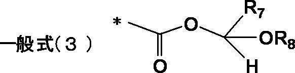
一般式(3)中、R7は、水素原子または置換基を有してもよいアルキル基を表す。アルキル基の定義および好適範囲は、上述したR1、R2、およびR3で表されるアルキル基と同義である。アルキル基に置換してもよい置換基の種類も上述した通りである。
R8は、置換基を有してもよいアルキル基を表す。アルキル基の定義および好適範囲は、上述したR1、R2、およびR3で表されるアルキル基と同義である。アルキル基に置換してもよい置換基の種類も上述した通りである。
なお、R7およびR8は、結合して環を形成してもよい。形成される環の種類としては、上述したR1、R2、およびR3で形成される環が挙げられる。 In General Formula (3), R 7 represents a hydrogen atom or an alkyl group which may have a substituent. The definition and preferred range of the alkyl group are the same as those of the alkyl group represented by R 1 , R 2 and R 3 described above. The types of substituents that may be substituted on the alkyl group are also as described above.
R 8 represents an alkyl group which may have a substituent. The definition and preferred range of the alkyl group are the same as those of the alkyl group represented by R 1 , R 2 and R 3 described above. The types of substituents that may be substituted on the alkyl group are also as described above.
R 7 and R 8 may combine to form a ring. Examples of the ring formed include the rings formed by R 1 , R 2 , and R 3 described above.
なお、R7およびR8の好適態様としては、経時安定性、デスミア耐性がより優れる点で、アルコキシ基、アルコキシカルボニル基、ハロゲン基等の電子吸引性基で置換されたアルキル基であることが好ましい。
また、R7およびR8の他の好適態様としては、R7が炭素数1~8のアルキル基、炭素数1~6のアルコキシ基を有する炭素数1~8のアルキル基、炭素数2~7のアルコキシカルボニル基を有する炭素数1~8のアルキル基、またはハロゲン基を有する炭素数1~8のアルキル基であり、R8が炭素数1~8のアルキル基、炭素数1~6のアルコキシ基を有する炭素数1~8のアルキル基、炭素数2~7のアルコキシカルボニル基を有する炭素数1~8のアルキル基、またはハロゲン基を有する炭素数1~8のアルキル基である態様が挙げられる。
なお、R7とR8とが結合して4~6員環の脂肪族炭化水素環を形成してもよい。 A preferred embodiment of R 7 and R 8 is an alkyl group substituted with an electron-withdrawing group such as an alkoxy group, an alkoxycarbonyl group, or a halogen group from the viewpoint of better temporal stability and desmear resistance. preferable.
In another preferred embodiment of R 7 and R 8 , R 7 is an alkyl group having 1 to 8 carbon atoms, an alkyl group having 1 to 8 carbon atoms having an alkoxy group having 1 to 6 carbon atoms, An alkyl group having 1 to 8 carbon atoms having 7 alkoxycarbonyl groups, or an alkyl group having 1 to 8 carbon atoms having a halogen group, and R 8 is an alkyl group having 1 to 8 carbon atoms, 1 to 6 carbon atoms, An embodiment in which the alkyl group is an alkyl group having 1 to 8 carbon atoms having an alkoxy group, an alkyl group having 1 to 8 carbon atoms having an alkoxycarbonyl group having 2 to 7 carbon atoms, or an alkyl group having 1 to 8 carbon atoms having a halogen group. Can be mentioned.
R 7 and R 8 may combine to form a 4- to 6-membered aliphatic hydrocarbon ring.
極性変換基Aの好ましい態様として、下記一般式(4)で表される基を有する態様が挙げられる。*は、結合位置を示す。
Preferred embodiments of the polar conversion group A include an embodiment having a group represented by the following general formula (4). * Indicates a binding position.

一般式(4)中、R9およびR10は、置換基を有してもよいアルキル基、または、置換基を有してもよいアリール基を表す。アルキル基としては、本発明の効果がより優れる点で、炭素数1~25が好ましく、炭素数1~8がより好ましい。より具体的には、メチル基、エチル基、イソプロピル基、t-ブチル基、シクロヘキシル基などの直鎖状、分岐状または環状のアルキル基が挙げられる。
アリール基の種類としては、上述したR1、R2、およびR3で表されるアリール基が挙げられる。 In general formula (4), R 9 and R 10 represent an alkyl group which may have a substituent or an aryl group which may have a substituent. The alkyl group preferably has 1 to 25 carbon atoms and more preferably 1 to 8 carbon atoms from the viewpoint that the effects of the present invention are more excellent. More specifically, a linear, branched or cyclic alkyl group such as a methyl group, an ethyl group, an isopropyl group, a t-butyl group and a cyclohexyl group can be mentioned.
Examples of the aryl group include the aryl groups represented by R 1 , R 2 , and R 3 described above.
なお、R9およびR10は、結合して環を形成してもよい。形成される環の種類としては、上述したR1、R2、およびR3で形成される環が挙げられる。
R 9 and R 10 may combine to form a ring. Examples of the ring formed include the rings formed by R 1 , R 2 , and R 3 described above.
上記アルキル基またはアリール基が置換基を有する場合、本発明の効果を損なわない限り、置換基の種類は特に制限されず、例えば、上述したR1、R2、およびR3で表されるアルキル基またはアリール基に置換される置換基などが例示される。
When the alkyl group or aryl group has a substituent, the type of the substituent is not particularly limited as long as the effects of the present invention are not impaired. For example, the alkyl represented by the above-described R 1 , R 2 , and R 3 Examples include a substituent substituted with a group or an aryl group.
R9およびR10の好適態様としては、経時安定性の点で、アルコキシ基、カルボニル基、アルコキシカルボニル基、シアノ基、ハロゲン基等の電子吸引性基で置換されたアルキル基、または、シクロヘキシル基、ノルボルニル基等の環状アルキル基が特に好ましい。物性値としては、重クロロホルム中、プロトンNMRにおける2級メチン水素のケミカルシフトが4.4ppmよりも低磁場に現れる化合物が好ましく、4.6ppmよりも低磁場に現れる化合物がより好ましい。このように、電子吸引性基で置換されたアルキル基が特に好ましいのは、熱分解反応時に中間体として生成していると思われるカルボカチオンが電子吸引性基により不安定化し、分解が抑制されるためであると考えられる。具体的には、-CHR9R10の構造としては、下記式で表される構造が特に好ましい。
As a preferable embodiment of R 9 and R 10 , an alkyl group substituted with an electron-withdrawing group such as an alkoxy group, a carbonyl group, an alkoxycarbonyl group, a cyano group, a halogen group, or a cyclohexyl group is preferable in terms of stability over time. A cyclic alkyl group such as a norbornyl group is particularly preferable. As a physical property value, a compound in which the chemical shift of secondary methine hydrogen in proton NMR in a deuterated chloroform appears in a magnetic field lower than 4.4 ppm is preferable, and a compound that appears in a magnetic field lower than 4.6 ppm is more preferable. Thus, an alkyl group substituted with an electron-withdrawing group is particularly preferred because the carbocation that appears to be formed as an intermediate during the thermal decomposition reaction is destabilized by the electron-withdrawing group and decomposition is suppressed. This is considered to be because of this. Specifically, the structure represented by the following formula is particularly preferable as the structure of —CHR 9 R 10 .

なお、極性変換基は、上述した一般式(1)~(4)のいずれかで表される基以外の基を有していてもよい。例えば、一般式(1)~(4)中の*にさらに連結基-L-が結合していてもよい。
連結基としては特に制限されず、例えば、2~4価の連結基が挙げられる。例えば、1から60個までの炭素原子、0個から10個までの窒素原子、0個から50個までの酸素原子、1個から100個までの水素原子、および0個から20個までの硫黄原子から成り立つ基が挙げられる。より具体的な連結基としては、下記の構造単位、および、それらが組み合わさって構成される基が挙げられる。
なお、これらの連結基は置換基を有していてもよい。置換基の種類は特に制限されないが、例えば、上述したR1、R2、およびR3で表されるアルキル基またはアリール基に置換される置換基などが例示される。 The polar conversion group may have a group other than the group represented by any one of the general formulas (1) to (4) described above. For example, a linking group —L— may be further bonded to * in the general formulas (1) to (4).
The linking group is not particularly limited, and examples thereof include divalent to tetravalent linking groups. For example, 1 to 60 carbon atoms, 0 to 10 nitrogen atoms, 0 to 50 oxygen atoms, 1 to 100 hydrogen atoms, and 0 to 20 sulfur atoms. Examples include groups consisting of atoms. More specific examples of the linking group include the following structural units and groups constituted by combining them.
In addition, these coupling groups may have a substituent. The type of the substituent is not particularly limited, and examples thereof include a substituent substituted with the alkyl group or aryl group represented by R 1 , R 2 , and R 3 described above.
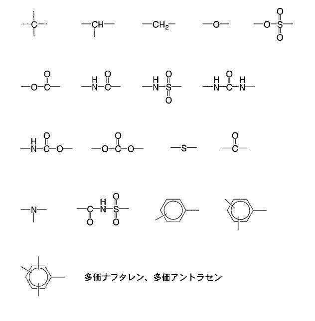
(B)極性変換基B
極性変換基Bとしては公知の官能基を使用することができ、例えば、700nm以下の光照射を行うことにより親疎水性が変化する官能基を使用することができる。このように、700nm以下の光照射により極性変換する官能基は、赤外線などの長波長露光や熱によらず、所定の波長の光照射により直接に、分解、開環または二量化反応が生じることで、高感度で疎水性から親水性が変化することを特徴とする。
該官能基としては、例えば、特開2004-175098号公報に記載の一般式(a)~(i)で表される官能基を用いることができる。 (B) Polarity converting group B
As the polarity converting group B, a known functional group can be used. For example, a functional group whose hydrophilicity / hydrophobicity is changed by irradiation with light of 700 nm or less can be used. In this way, functional groups that undergo polarity conversion upon irradiation with light of 700 nm or less can directly undergo decomposition, ring opening, or dimerization reaction upon irradiation with light of a predetermined wavelength, regardless of long-wavelength exposure such as infrared rays or heat. in, wherein the hydrophilic changes from hydrophobic at high sensitivity.
As the functional group, for example, functional groups represented by general formulas (a) to (i) described in JP-A No. 2004-175098 can be used.
極性変換基の具体例を以下に示す。
Specific examples of polar conversion groups are shown below.
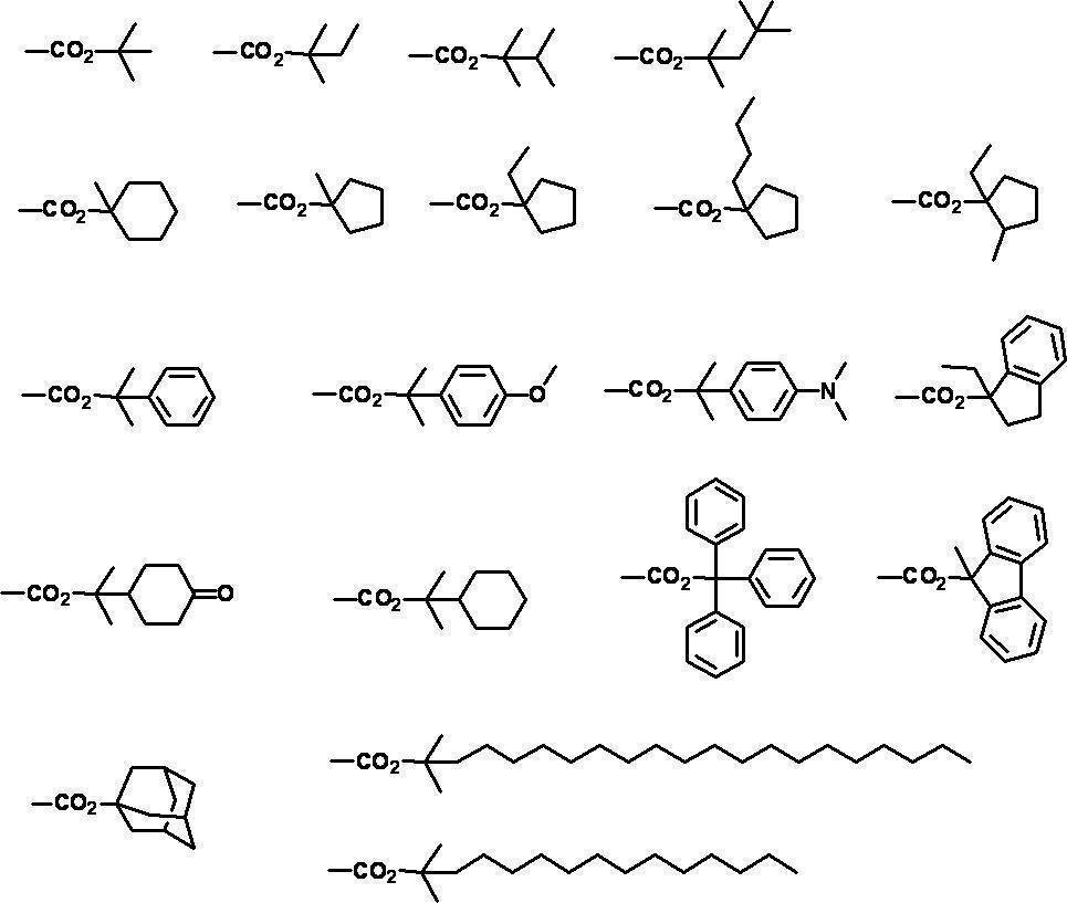
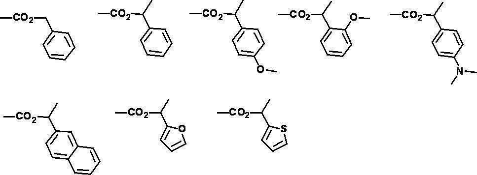


極性変換基を有するポリマーの骨格の種類は特に制限されないが、例えば、ポリイミド樹脂、エポキシ樹脂、ウレタン樹脂、ポリエチレン樹脂、ポリエステル樹脂、ウレタン樹脂、ノボラック樹脂、クレゾール樹脂、アクリル樹脂、メタアクリル樹脂、スチレン樹脂などが挙げられる。なかでも、材料の入手性や、成膜性などの点で、アクリル樹脂、メタアクリル樹脂が好ましい。
The type of polymer skeleton having a polar conversion group is not particularly limited. For example, polyimide resin, epoxy resin, urethane resin, polyethylene resin, polyester resin, urethane resin, novolac resin, cresol resin, acrylic resin, methacrylic resin, styrene Resin etc. are mentioned. Of these, acrylic resins and methacrylic resins are preferable in terms of availability of materials and film formability.
ポリマーの重量平均分子量は特に制限されないが、被めっき層の成膜性などの点から、5000~50万が好ましく、1万~30万がより好ましい。
なお、該ポリマーは、実質的にシアノ基を有さないことが好ましく、シアノ基が含まれないことがより好ましい。ポリマー中にシアノ基が含まれていると、後述するデスミア工程の際に、シアノ基が酸化されてカルボン酸などの親水性基へと変換する場合がある。この場合、デスミア処理液に対する耐性が弱くなる場合がある。なお、シアノ基を実質的に有しないとは、ポリマー中におけるシアノ基の含有量が0.1質量%以下であることを意味する。 The weight average molecular weight of the polymer is not particularly limited, but is preferably from 5,000 to 500,000, more preferably from 10,000 to 300,000, from the viewpoint of film formability of the layer to be plated.
In addition, it is preferable that this polymer does not have a cyano group substantially, and it is more preferable that a cyano group is not contained. If the polymer contains a cyano group, the cyano group may be oxidized and converted to a hydrophilic group such as a carboxylic acid during the desmear process described later. In this case, the resistance to the desmear treatment liquid may be weakened. In addition, having substantially no cyano group means that the content of the cyano group in the polymer is 0.1% by mass or less.
(極性変換基を有するポリマーの好適態様:その1)
極性変換基を有するポリマーの好適態様の一つとしては、以下の一般式(A)で表されるユニット(極性変換基ユニットとも称する)を有することが好ましい。ポリマーが該ユニットを有する場合、金属層の密着性がより向上する。 (Preferred embodiment of polymer having polar conversion group: Part 1)
As a preferred embodiment of the polymer having a polar conversion group, it is preferable to have a unit represented by the following general formula (A) (also referred to as a polar conversion group unit). When a polymer has this unit, the adhesiveness of a metal layer improves more.

一般式(A)中、R11は、水素原子、または、炭素数1~4の置換若しくは無置換のアルキル基を表す。アルキル基としては、メチル基、エチル基などが挙げられる。
一般式(A)中、L1は、単結合または二価の有機基を表す。二価の有機基としては、置換若しくは無置換の二価の脂肪族炭化水素基(好ましくは炭素数1~8。例えば、メチレン基、エチレン基、プロピレン基などのアルキレン基)、置換若しくは無置換の二価の芳香族炭化水素基(好ましくは炭素数6~12。例えば、フェニレン基)、-O-、-S-、-SO2-、-N(R)-(R:アルキル基)、-CO-、-NH-、-COO-、-CONH-、またはこれらを組み合わせた基(例えば、アルキレンオキシ基、アルキレンオキシカルボニル基、アルキレンカルボニルオキシ基など)などが挙げられる。なかでも、本発明の効果がより優れる点で、単結合、芳香族炭化水素基が好ましい。 In general formula (A), R 11 represents a hydrogen atom or a substituted or unsubstituted alkyl group having 1 to 4 carbon atoms. Examples of the alkyl group include a methyl group and an ethyl group.
In the general formula (A), L 1 represents a single bond or a divalent organic group. Examples of the divalent organic group include a substituted or unsubstituted divalent aliphatic hydrocarbon group (preferably having 1 to 8 carbon atoms, for example, an alkylene group such as a methylene group, an ethylene group, and a propylene group), a substituted or unsubstituted group. A divalent aromatic hydrocarbon group (preferably having 6 to 12 carbon atoms, such as a phenylene group), —O—, —S—, —SO 2 —, —N (R) — (R: alkyl group), And —CO—, —NH—, —COO—, —CONH—, or a combination thereof (for example, an alkyleneoxy group, an alkyleneoxycarbonyl group, an alkylenecarbonyloxy group, and the like). Especially, a single bond and an aromatic hydrocarbon group are preferable at the point which the effect of this invention is more excellent.
一般式(A)中、Yは、上述した極性変換基を表す。なかでも、金属層の密着性がより優れる点で、一般式(1)~(4)のいずれかで表される基であることが好ましい。
In general formula (A), Y represents the polar conversion group described above. Among these, a group represented by any one of the general formulas (1) to (4) is preferable from the viewpoint of better adhesion of the metal layer.
上記一般式(A)で表されるユニットの好適態様の一つとして、金属層の密着性がより優れる点で、以下の一般式(A-1)で表されるユニットが挙げられる。
One preferred embodiment of the unit represented by the general formula (A) is a unit represented by the following general formula (A-1) in that the adhesion of the metal layer is more excellent.
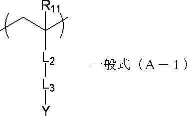
一般式(A-1)中、R11およびYの定義は上述の通りである。
L2は、単結合、アミド基(-CONH-)、エステル基、またはフェニレン基を表す。L3は、単結合、または、脂肪族炭化水素基を表す。なお、L2がアミド基またはエステル基の場合、L3は脂肪族炭化水素基を表す。 In the general formula (A-1), the definition of R 11 and Y are as described above.
L 2 represents a single bond, an amide group (—CONH—), an ester group, or a phenylene group. L 3 represents a single bond or an aliphatic hydrocarbon group. Note that when L 2 is an amide group or an ester group, L 3 represents an aliphatic hydrocarbon group.
ポリマー中における一般式(A)で表されるユニット(または、一般式(A-1)で表されるユニット)の含有量は特に制限されないが、金属層の密着性がより優れる点で、全ポリマーユニット中、10~95モル%が好ましく、55~90モル%がより好ましい。
The content of the unit represented by the general formula (A) in the polymer (or the unit represented by the general formula (A-1)) is not particularly limited. However, in terms of better adhesion of the metal layer, In the polymer unit, 10 to 95 mol% is preferable, and 55 to 90 mol% is more preferable.
(極性変換基を有するポリマーの好適態様:その2)
極性変換基を有するポリマーの他の好適態様として、極性変換基および架橋性基を有するポリマーが挙げられる。ポリマーが架橋性基を有する場合、架橋性基を介した架橋反応により、強度に優れ、より疎水性の被めっき層を得ることができ、結果として金属層の密着性が向上する。 (Preferred embodiment of polymer having polar conversion group: Part 2)
As another preferred embodiment of the polymer having a polar converting group, a polymer having a polar converting group and a crosslinkable group can be mentioned. When the polymer has a crosslinkable group, it is possible to obtain a layer having a higher strength and a more hydrophobic layer by a crosslink reaction via the crosslinkable group, and as a result, the adhesion of the metal layer is improved.
ポリマー中に含まれる架橋性基の位置は特に制限されず、例えば、ポリマーの末端または側鎖が挙げられる。
架橋性基の種類は特に制限されず、例えば、山下信二編「架橋剤ハンドブック」に掲載されているような従来公知の架橋性基(架橋反応に用いられる構造を有する官能基)を使用することができる。
これらの従来公知の架橋性基の中でも、金属層の密着性がより優れる点で、カルボン酸基(-COOH)、ヒドロキシル基(-OH)、イソシアネート基(-NCO)、シラノール基(Si-OH)、アルコキシシリル基、アセトキシシリル基、クロロシリル基、1級アミノ基(-NH2)、2級アミノ基(-NHRb(なお、Rbは置換基(好ましくは、炭化水素基)を表す。))、3級アミノ基(-NRbRc(なお、RbおよびRcは、それぞれ独立に、置換基(好ましくは、炭化水素基)を表す。))、エポキシ基、オキセタニル基、エチレン付加重合性不飽和基(なかでも、本発明の効果がより優れる点で、(メタ)アクリルアミド基が好ましい)が好ましい。架橋性基のなかでも、被めっき層のデスミア耐性がより優れる点で、カルボキシル基、ヒドロキシル基、イソシアネート基、アルコキシシリル基、アセトキシシリル基、クロロシリル基、3級アミノ基、エポキシ基、またはオキセタニル基がより好ましく、エポキシ基、オキセタニル基、アルコキシシリル基が特に好ましい。 The position in particular of the crosslinkable group contained in a polymer is not restrict | limited, For example, the terminal or side chain of a polymer is mentioned.
The type of the crosslinkable group is not particularly limited. For example, a conventionally known crosslinkable group (functional group having a structure used for the crosslinking reaction) as described in Shinji Yamashita “Crosslinking agent handbook” is used. Can do.
Among these conventionally known crosslinkable groups, a carboxylic acid group (—COOH), a hydroxyl group (—OH), an isocyanate group (—NCO), a silanol group (Si—OH) is used because the adhesion of the metal layer is more excellent. ), An alkoxysilyl group, an acetoxysilyl group, a chlorosilyl group, a primary amino group (—NH 2 ), a secondary amino group (—NHR b (where R b represents a substituent (preferably a hydrocarbon group)). )) Tertiary amino group (—NR b R c (wherein R b and R c each independently represents a substituent (preferably a hydrocarbon group))), epoxy group, oxetanyl group, ethylene Addition-polymerizable unsaturated groups (in particular, (meth) acrylamide groups are preferred from the viewpoint that the effects of the present invention are more excellent) are preferred. Among the crosslinkable groups, a carboxyl group, a hydroxyl group, an isocyanate group, an alkoxysilyl group, an acetoxysilyl group, a chlorosilyl group, a tertiary amino group, an epoxy group, or an oxetanyl group in that the desmear resistance of the plated layer is more excellent. Are more preferable, and an epoxy group, an oxetanyl group, and an alkoxysilyl group are particularly preferable.
アルコキシシリル基とは、ケイ素原子にアルコキシ基が結合した基(-Si-ORd(Rd:アルキル基)を意味する。アセトキシシリル基とは、ケイ素原子にアセトキシ基が結合した基を意味する。クロロシリル基とは、ケイ素原子に塩素原子が結合した基を意味する。
The alkoxysilyl group means a group in which an alkoxy group is bonded to a silicon atom (—Si—OR d (R d : alkyl group). The acetoxysilyl group means a group in which an acetoxy group is bonded to a silicon atom. The chlorosilyl group means a group in which a chlorine atom is bonded to a silicon atom.
極性変換基および架橋性基を有するポリマーの好適態様としては、一般式(B)で表されるユニット(架橋性基ユニットとも称する)を有するポリマーが挙げられる。ポリマーが該ユニットを有する場合、金属層の密着性がより向上する。
Preferred examples of the polymer having a polar conversion group and a crosslinkable group include a polymer having a unit represented by the general formula (B) (also referred to as a crosslinkable group unit). When a polymer has this unit, the adhesiveness of a metal layer improves more.

一般式(B)中、R12は、水素原子、または、炭素数1~4の置換若しくは無置換のアルキル基を表す。アルキル基としては、メチル基、エチル基などが挙げられる。
一般式(B)中、L4は、単結合または二価の有機基を表す。該有機基の定義は、L1で表される有機基の定義と同義である。
一般式(B)中、Zは、カルボン酸基、ヒドロキシル基、イソシアネート基、シラノール基、アルコキシシリル基、アセトキシシリル基、クロロシリル基、1級アミノ基、2級アミノ基、3級アミノ基、エポキシ基、オキセタニル基、または以下の一般式(C)で表される基を表す。なかでも、デスミア耐性に優れ、得られる金属層の密着性がより優れる点で、エポキシ基、オキセタニル基、アルコキシシリル基がより好ましい。 In the general formula (B), R 12 represents a hydrogen atom or a substituted or unsubstituted alkyl group having 1 to 4 carbon atoms. Examples of the alkyl group include a methyl group and an ethyl group.
In the general formula (B), L 4 represents a single bond or a divalent organic group. Definition of the organic groups are the same as those defined organic group represented by L 1.
In general formula (B), Z is a carboxylic acid group, a hydroxyl group, an isocyanate group, a silanol group, an alkoxysilyl group, an acetoxysilyl group, a chlorosilyl group, a primary amino group, a secondary amino group, a tertiary amino group, an epoxy. Represents a group, an oxetanyl group, or a group represented by the following general formula (C). Especially, an epoxy group, an oxetanyl group, and an alkoxysilyl group are more preferable at the point which is excellent in desmear tolerance and the adhesiveness of the metal layer obtained is more excellent.
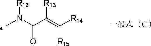
一般式(C)中、R13~R15は、それぞれ独立して、水素原子、または炭素数1~4の置換若しくは無置換のアルキル基を表す。アルキル基としては、例えば、メチル基、エチル基などが挙げられる。
In formula (C), R 13 to R 15 each independently represents a hydrogen atom or a substituted or unsubstituted alkyl group having 1 to 4 carbon atoms. Examples of the alkyl group include a methyl group and an ethyl group.
一般式(C)中、R16は、水素原子、アルキル基(好ましくは炭素数1~8)、アルケニル基(好ましくは炭素数1~8)、アルキニル基(好ましくは炭素数1~8)、またはアリール基を表す。なかでも、本発明の効果がより優れる点で、アルキル基、アリール基がより好ましい。
In the general formula (C), R 16 is a hydrogen atom, an alkyl group (preferably having 1 to 8 carbon atoms), an alkenyl group (preferably having 1 to 8 carbon atoms), an alkynyl group (preferably having 1 to 8 carbon atoms), Or represents an aryl group. Among them, in terms of the effect of the present invention is more excellent, an alkyl group, an aryl group are more preferable.
上記一般式(B)で表されるユニットの好適態様の一つとして、金属層の密着性がより優れる点で、以下の一般式(B-1)で表されるユニットが挙げられる。
One preferred embodiment of the unit represented by the general formula (B) is a unit represented by the following general formula (B-1) in that the adhesion of the metal layer is more excellent.

一般式(B-1)中、R12およびZの定義は上述の通りである。
L5は、単結合、アミド基、エステル基、またはフェニル基を表す。L6は、単結合、または、-O-、-COO-、-CONH-結合で介されていてもよい炭素数1~8の脂肪族炭化水素基を表す。なお、Zがカルボキシル基の場合、L5、L6はともに単結合であってもよい。 In the general formula (B-1), the definition of R 12 and Z are as described above.
L 5 represents a single bond, an amide group, an ester group, or a phenyl group. L 6 represents a single bond or an aliphatic hydrocarbon group having 1 to 8 carbon atoms which may be bonded via a —O—, —COO— or —CONH— bond. When Z is a carboxyl group, both L 5 and L 6 may be a single bond.
ポリマー中における一般式(B)で表されるユニット(または、一般式(B-1)で表されるユニット)の含有量は特に制限されないが、金属層の密着性がより優れる点で、全ポリマーユニット中、5~90モル%が好ましく、10~45モル%がより好ましい。
The content of the unit represented by the general formula (B) in the polymer (or the unit represented by the general formula (B-1)) is not particularly limited. However, in terms of better adhesion of the metal layer, In the polymer unit, 5 to 90 mol% is preferable, and 10 to 45 mol% is more preferable.
なお、金属層の密着性がより向上する点で、ポリマーの態様として一般式(A)で表されるユニットおよび一般式(B)で表されるユニットを有するポリマーが挙げられる。なかでも、上記ポリマーの態様として最も好ましくは、上記一般式(A-1)で表されるユニットおよび一般式(B-1)で表されるユニットを有するポリマーが挙げられる。
該態様の場合、一般式(A-1)で表されるユニット中、L2は、単結合またはフェニレン基で、L3が単結合で、Yが一般式(1)~(4)のいずれかで表される基で、R11が水素原子であり、一般式(B-1)で表されるユニット中、L5がアミド基、エステル基、またはフェニル基であり、L6が炭素数1~8の脂肪族炭化水素基、または、-O-、-COO-、-CONH-結合で介された炭素数1~8の脂肪族炭化水素基であり、Zがヒドロキシル基、イソシアネート基、アルコキシシリル基、3級アミノ基、エポキシ基、またはオキセタニル基であり、R12が水素原子またはメチル基であることが好ましい。 In addition, the polymer which has a unit represented by the unit represented by general formula (A) and a general formula (B) as a polymer aspect at the point which the adhesiveness of a metal layer improves more is mentioned. Among these, the polymer having the unit represented by the general formula (A-1) and the unit represented by the general formula (B-1) is most preferable as an embodiment of the polymer.
In this embodiment, in the unit represented by the general formula (A-1), L 2 is a single bond or a phenylene group, L 3 is a single bond, and Y is any one of the general formulas (1) to (4). R 11 is a hydrogen atom, and in the unit represented by the general formula (B-1), L 5 is an amide group, an ester group, or a phenyl group, and L 6 is a carbon number An aliphatic hydrocarbon group having 1 to 8 carbon atoms or an aliphatic hydrocarbon group having 1 to 8 carbon atoms via a —O—, —COO—, or —CONH— bond, and Z is a hydroxyl group, an isocyanate group, It is preferably an alkoxysilyl group, a tertiary amino group, an epoxy group, or an oxetanyl group, and R 12 is preferably a hydrogen atom or a methyl group.
(極性変換基を有するポリマーの合成方法)
極性変換基を有するポリマーの合成方法は特に制限されず、公知の方法(例えば、ラジカル重合、カチオン重合など)を使用できる。より具体的には、極性変換基を有するモノマーを重合して該ポリマーを得ることができる。
使用されるモノマーとしては、例えば、以下のモノマーが挙げられる。 (Method of synthesizing a polymer having a polarity conversion group)
The method for synthesizing the polymer having a polarity converting group is not particularly limited, and a known method (for example, radical polymerization, cationic polymerization, etc.) can be used. More specifically, the polymer can be obtained by polymerizing a monomer having a polarity converting group.
Examples of the monomer used include the following monomers.


極性変換基および架橋性基を有するポリマーの合成方法は特に制限されず、例えば、官極性変換基を有するモノマーと、架橋性基を有するモノマーとを共重合させる方法が挙げられる。使用される架橋性基を有するモノマーとしては、例えば、以下のモノマーが挙げられる。
The method for synthesizing a polymer having a polar conversion group and a crosslinkable group is not particularly limited, and examples thereof include a method of copolymerizing a monomer having a public polarity conversion group and a monomer having a crosslinkable group. Examples of the monomer having a crosslinkable group used include the following monomers.

また、架橋性基としてエチレン付加重合性不飽和基が使用される場合、例えば、特開2009-007540号公報などに記載の方法を参照してポリマーを合成することができる。
Further, when an ethylene addition polymerizable unsaturated group is used as the crosslinkable group, for example, a polymer can be synthesized by referring to a method described in JP-A-2009-007540.
極性変換基と架橋性基とを有するポリマーの好ましい態様としては、上記極性変換基を有するモノマーと上記架橋性基を有するモノマーを共重合することで合成したポリマーが挙げられる。具体例を以下に示すが、これらのポリマーに限定される訳ではない。なお、下記に示すポリマー中の繰り返し単位に併記された数値は、各ユニットのモル%を示す。
A preferred embodiment of the polymer having a polar conversion group and a crosslinkable group includes a polymer synthesized by copolymerizing the monomer having the polar conversion group and the monomer having the crosslinkable group. Specific examples are shown below, but are not limited to these polymers. In addition, the numerical value written together by the repeating unit in the polymer shown below shows mol% of each unit.
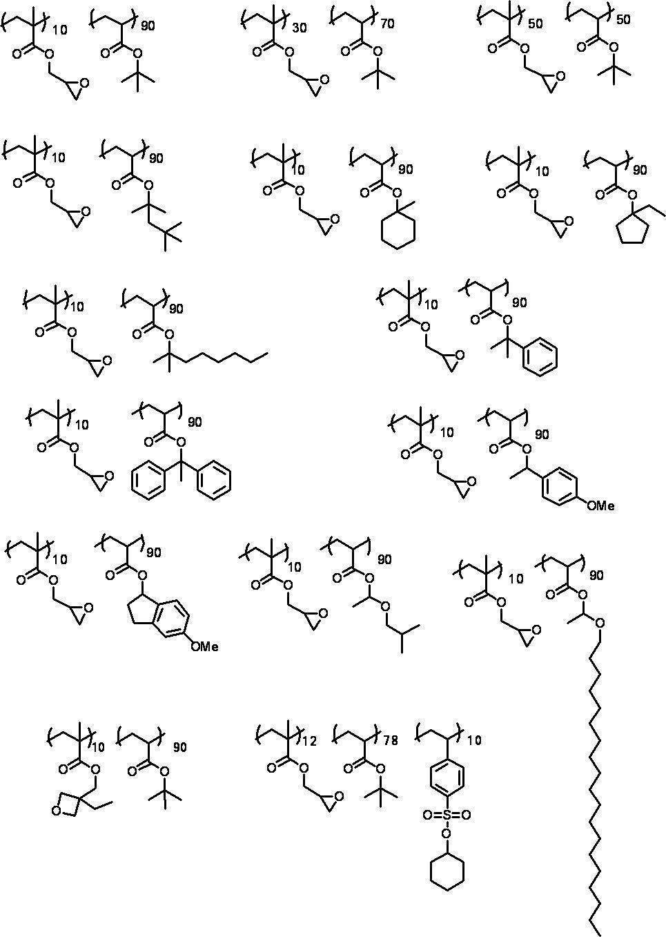


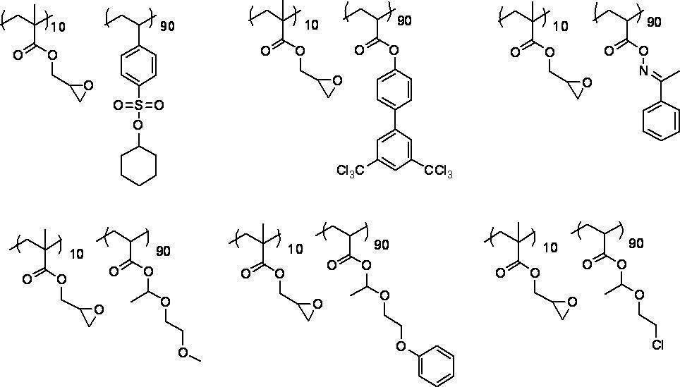
[工程(A)の手順]
上記導電層付き基板の導電層側上に極性変換基を有する化合物を含む被めっき層を形成する方法は、特に制限されず公知の方法を採用できる。例えば、極性変換基を有する化合物を含む被めっき層形成用組成物を導電層付き基板上に塗布し、被めっき層を形成する方法(塗布方法)、該化合物(例えば、ポリマー)を直接導電層付き基板上にラミネートする方法などが挙げられる。なかでも、被めっき層の膜厚制御が容易である点から、塗布方法が好ましい。
以後、塗布方法の態様について詳述する。 [Procedure of step (A)]
A method for forming a plated layer containing a compound having a polarity conversion group on the conductive layer side of the substrate with the conductive layer is not particularly limited, and a known method can be adopted. For example, a method for forming a layer to be plated (coating method) by applying a composition for forming a layer to be plated containing a compound having a polarity conversion group onto a substrate with a conductive layer, and applying the compound (for example, polymer) directly to the conductive layer For example, a method of laminating on the attached substrate can be mentioned. Especially, the coating method is preferable from the point that the film thickness control of a to-be-plated layer is easy.
Hereinafter, the aspect of the coating method will be described in detail.
塗布方法で使用される被めっき層形成用組成物には、上記極性変換基を有する化合物が含有される。
被めっき層形成用組成物中の該化合物の含有量は特に制限されないが、組成物全量に対して、2~50質量%が好ましく、5~30質量%がより好ましい。上記範囲内であれば、組成物の取扱い性に優れ、被めっき層の層厚の制御がしやすい。 The composition for forming a plating layer used in the coating method contains the compound having the polarity converting group.
The content of the compound in the composition for forming a layer to be plated is not particularly limited, but is preferably 2 to 50% by mass and more preferably 5 to 30% by mass with respect to the total amount of the composition. If it is in the said range, it is excellent in the handleability of a composition and it is easy to control the layer thickness of a to-be-plated layer.
被めっき層形成用組成物は、必要に応じて、溶剤を含んでいてもよい。
使用できる溶剤としては、例えば、水、メタノール、エタノール、プロパノール、エチレングリコール、グリセリン、プロピレングリコールモノメチルエーテル等のアルコール系溶剤;酢酸等の酸;アセトン、メチルエチルケトン、シクロヘキサノン等のケトン系溶剤;ホルムアミド、ジメチルアセトアミド、N-メチルピロリドン等のアミド系溶剤;アセトニトリル、プロピオニトリル等のニトリル系溶剤;酢酸メチル、酢酸エチル、プロピレングリコールモノメチルエーテルアセタート等のエステル系溶剤;ジメチルカーボネート、ジエチルカーボネート等のカーボネート系溶剤が挙げられる。
また取り扱いやすさの点から、沸点が50℃~150℃の溶剤が好ましい。なお、これらの溶剤は単一で使用してもよいし、混合して使用してもよい。 To be plated layer forming composition, if desired, it may contain a solvent.
Examples of solvents that can be used include alcohol solvents such as water, methanol, ethanol, propanol, ethylene glycol, glycerin, and propylene glycol monomethyl ether; acids such as acetic acid; ketone solvents such as acetone, methyl ethyl ketone, and cyclohexanone; formamide and dimethyl Amide solvents such as acetamide and N-methylpyrrolidone; Nitrile solvents such as acetonitrile and propionitrile; Ester solvents such as methyl acetate, ethyl acetate and propylene glycol monomethyl ether acetate; Carbonates such as dimethyl carbonate and diethyl carbonate A solvent is mentioned.
From the viewpoint of ease of handling, a solvent having a boiling point of 50 ° C. to 150 ° C. is preferable. Incidentally, the these solvents may be used singly, it may be used as a mixture.
被めっき層形成用組成物は、後述する架橋剤、後述する光酸発生剤、界面活性剤、可塑剤、重合禁止剤、硬化を進めるための重合開始剤、硬化促進剤、ゴム成分(例えば、CTBN)、難燃化剤(例えば、りん系難燃化剤)、希釈剤、チキソトロピー化剤、顔料、消泡剤、レべリング剤、カップリング剤などを含有していてもよい。
また、被めっき層形成用組成物は、本発明の効果を阻害しない範囲で、特開2009-7540号公報、または特開2010‐248464号公報に記載の重合性基と触媒吸着性基を有するポリマーを含有していてもよい。 The composition for forming a layer to be plated includes a crosslinking agent described later, a photoacid generator described later, a surfactant, a plasticizer, a polymerization inhibitor, a polymerization initiator for proceeding with curing, a curing accelerator, a rubber component (for example, CTBN), a flame retardant (for example, a phosphorus flame retardant), a diluent, a thixotropic agent, a pigment, an antifoaming agent, a leveling agent, a coupling agent, and the like.
In addition, the composition for forming a layer to be plated has a polymerizable group and a catalyst adsorbing group described in JP2009-7540A or JP2010-248464A as long as the effects of the present invention are not impaired. It may contain a polymer.
被めっき層形成用組成物を導電層付き基板上に塗布する方法は特に限定されず、公知の方法(例えば、スピンコート、デップコート、ダブルロールコータ、スリットコータ、エアナイフコータ、ワイヤーバーコータなど)を用いることができる。
取り扱い性や製造効率の観点からは、被めっき層形成用組成物を導電層付き基板上に塗布して、必要に応じて乾燥処理を施して含まれる溶剤を除去し、被めっき層を形成する態様が好ましい。 The method for applying the composition for forming a layer to be plated on the substrate with the conductive layer is not particularly limited, and a known method (for example, spin coating, dip coating, double roll coater, slit coater, air knife coater, wire bar coater, etc.) Can be used.
From the viewpoint of handleability and production efficiency, the composition for forming a layer to be plated is applied on a substrate with a conductive layer, and if necessary, a drying treatment is performed to remove the solvent contained therein to form a layer to be plated. Embodiments are preferred.
被めっき層の厚みは特に制限されないが、金属層の密着性がより優れる点から、0.02~5.0μmが好ましく、0.05~2.0μmがより好ましい。
被めっき層中における極性変換基を有する化合物の含有量は特に制限されないが、金属層の密着性がより優れる点から、被めっき層全量に対して、10~100質量%であることが好ましく、50~100質量%であることがより好ましい。 The thickness of the layer to be plated is not particularly limited, but is preferably 0.02 to 5.0 μm, more preferably 0.05 to 2.0 μm, from the viewpoint of better adhesion of the metal layer.
The content of the compound having a polarity converting group in the layer to be plated is not particularly limited, but is preferably 10 to 100% by mass with respect to the total amount of the layer to be plated, from the viewpoint of better adhesion of the metal layer. and more preferably 50 to 100 mass%.
(被めっき層の好適態様)
上記被めっき層が極性変換基と架橋性基とを有するポリマーを含む場合、該層に対してさらに硬化処理を施すこと(工程(G))が好ましい。言い換えると、上記被めっき層は、極性変換基と架橋性基とを有するポリマーを架橋反応(硬化反応)により硬化させて得られる層であることが好ましい。該態様の場合、架橋性基を介して層の硬化が進行し、被めっき層自体の膜強度が高くなると共に疎水性も高まり、デスミア処理に対する耐性が向上する。結果として、金属層の密着性がより優れる。
以後、工程(G)の態様について詳述する。 (Preferred embodiment of the layer to be plated)
When the said layer to be plated contains the polymer which has a polar conversion group and a crosslinkable group, it is preferable to perform a hardening process with respect to this layer (process (G)). In other words, the layer to be plated is preferably a layer obtained by curing a polymer having a polarity converting group and a crosslinkable group by a crosslinking reaction (curing reaction). In the case of this mode, the curing of the layer proceeds through the crosslinkable group, the film strength of the layer to be plated itself is increased, the hydrophobicity is also increased, and the resistance to desmear treatment is improved. As a result, the adhesion of the metal layer is more excellent.
Hereinafter, the aspect of the step (G) will be described in detail.
硬化工程(工程(G))は、本工程(A)の後であって、後述する工程(E)の前に実施することが好ましい。より具体的には、工程(A)と工程(B)との間、工程(B)と工程(C)との間、工程(C)と工程(D)の間、または、工程(D)と工程(E)との間である。工程(E)の前に実施することによって、工程(E)で使用されるめっき触媒液や、工程(F)で使用されるめっき液に対する被めっき層の耐性を高めることができる。
なお、他の工程での被めっき層の溶出や分解を抑制できる点で、工程(A)と工程(B)との間に工程(G)を実施することが好ましい。 It is preferable to implement a hardening process (process (G)) after this process (A), and before the process (E) mentioned later. More specifically, between step (A) and step (B), between step (B) and step (C), between step (C) and step (D), or step (D). it is between the step (E). By carrying out before the step (E), the resistance of the plating layer to the plating catalyst solution used in the step (E) and the plating solution used in the step (F) can be increased.
In addition, it is preferable to implement a process (G) between a process (A) and a process (B) at the point which can suppress the elution and decomposition | disassembly of the to-be-plated layer in another process.
工程(G)におけるポリマーの架橋方法はポリマー中の架橋性基の種類によって適宜最適な方法が選択されるが、例えば、架橋性基同士を反応させる方法や、架橋剤を使用する方法が挙げられる。
As the method for crosslinking the polymer in the step (G), an optimum method is appropriately selected depending on the kind of the crosslinkable group in the polymer, and examples thereof include a method of reacting crosslinkable groups with each other and a method of using a crosslinking agent. .
架橋性基同士を反応させる方法は、架橋性基同士の付加反応や縮合反応を介して被めっき層中に架橋構造を形成する方法である。例えば、架橋性基が-NCOである場合、熱をかけることにより自己縮合反応を進行させ、被めっき層中に架橋構造を形成することができる。
The method of reacting crosslinkable groups is a method of forming a crosslinked structure in the layer to be plated through an addition reaction or a condensation reaction between the crosslinkable groups. For example, when the crosslinkable group is —NCO, a self-condensation reaction can be advanced by applying heat to form a crosslinked structure in the layer to be plated.
架橋剤を使用する方法は、ポリマー中の架橋性基と、該架橋性基と反応する反応性官能基を有する架橋剤の反応性官能基とを反応させ、被めっき層中に架橋構造を形成する方法である。
The method using a crosslinking agent is to form a crosslinked structure in the layer to be plated by reacting the crosslinking group in the polymer with the reactive functional group of the crosslinking agent having a reactive functional group that reacts with the crosslinking group. It is a method to do.
使用される架橋剤としては、山下信二編「架橋剤ハンドブック」に掲載されているような従来公知のものを用いることができる。より具体的には、架橋剤は、通常、架橋性基と反応する反応性官能基を2個以上有し、2~6個有することが好ましい。
反応性官能基としては、例えば、水酸基、イソシアネート基、カルボン酸基、エポキシ基、カルボン酸無水物基、1級アミノ基、2級アミノ基、アルコキシシリル基、ハロゲン化ベンジル基などが挙げられる。 As the crosslinking agent to be used, those conventionally known as described in Shinji Yamashita “Crosslinking agent handbook” can be used. More specifically, the crosslinking agent usually has 2 or more reactive functional groups that react with the crosslinkable group, and preferably has 2 to 6 reactive functional groups.
Examples of the reactive functional group include a hydroxyl group, an isocyanate group, a carboxylic acid group, an epoxy group, a carboxylic anhydride group, a primary amino group, a secondary amino group, an alkoxysilyl group, and a benzyl halide group.
ポリマー中の架橋性基と架橋剤中の反応性官能基との好ましい組み合わせとしては、例えば、(架橋性基,反応性官能基)=(カルボキシル基,一級または二級アミノ基)、(カルボキシル基,アジリジン基)、(カルボキシル基,イソシアネート基)、(カルボキシル基,エポキシ基)、(カルボキシル基,ハロゲン化ベンジル基)、(一級または二級アミノ基,イソシアネート基)、(一級、二級、または三級アミノ基,ハロゲン化ベンジル基)、(一級アミノ基,アルデヒド類)、(イソシアネート基,一級または二級アミノ基)、(イソシアネート基,イソシアネート基)、(イソシアネート基,水酸基)、(イソシアネート基,エポキシ基)、(水酸基,イソシアネート基)、(水酸基,ハロゲン化ベンジル基)、(水酸基,カルボン酸無水物基)、(水酸基,エポキシ基)、(水酸基,アルコキシシリル基)、(エポキシ基,一級または二級アミノ基)、(エポキシ基,カルボン酸無水物基)、(エポキシ基,水酸基)、(エポキシ基,エポキシ基)、(オキセタニル基,エポキシ基)、(アルコキシシリル基,アルコキシシリル基)などが挙げられる。なかでも、被めっき層のデスミア耐性がより優れる点で、(架橋性基,反応性官能基)=(エポキシ基,アミノ基)、(エポキシ基,エポキシ基)、(三級アミノ基,ハロゲン化ベンジル基)、(水酸基,イソシアネート基)、(オキセタニル基,エポキシ基)、(アルコキシシリル基、アルコキシシリル基)が、より好ましい組み合わせである。
As a preferable combination of the crosslinkable group in the polymer and the reactive functional group in the crosslinking agent, for example, (crosslinkable group, reactive functional group) = (carboxyl group, primary or secondary amino group), (carboxyl group) , Aziridine group), (carboxyl group, isocyanate group), (carboxyl group, epoxy group), (carboxyl group, halogenated benzyl group), (primary or secondary amino group, isocyanate group), (primary, secondary, or Tertiary amino group, halogenated benzyl group), (primary amino group, aldehydes), (isocyanate group, primary or secondary amino group), (isocyanate group, isocyanate group), (isocyanate group, hydroxyl group), (isocyanate group) , Epoxy group), (hydroxyl group, isocyanate group), (hydroxyl group, halogenated benzyl group), (hydroxyl group, carboxyl group) Boronic acid anhydride group), (hydroxyl group, epoxy group), (hydroxyl group, alkoxysilyl group), (epoxy group, primary or secondary amino group), (epoxy group, carboxylic acid anhydride group), (epoxy group, hydroxyl group) ), (Epoxy group, epoxy group), (oxetanyl group, epoxy group), (alkoxysilyl group, alkoxysilyl group) and the like. Among these, (crosslinkable group, reactive functional group) = (epoxy group, amino group), (epoxy group, epoxy group), (tertiary amino group, halogenated) in that the desmear resistance of the plated layer is more excellent (Benzyl group), (hydroxyl group, isocyanate group), (oxetanyl group, epoxy group), (alkoxysilyl group, alkoxysilyl group) are more preferred combinations.
架橋剤の使用量としては、通常、架橋性基のモル数に対して、0.01~50当量が好ましく、0.1~5当量がより好ましく、0.8~2当量が更に好ましい。
架橋剤の使用量が上記範囲内の場合、デスミア耐性とめっき液に対する被めっき層の耐性とを両立することができる。 The amount of the crosslinking agent used is usually preferably 0.01 to 50 equivalents, more preferably 0.1 to 5 equivalents, still more preferably 0.8 to 2 equivalents, relative to the number of moles of the crosslinkable group.
When the usage-amount of a crosslinking agent is in the said range, desmear tolerance and the tolerance of the to-be-plated layer with respect to a plating solution can be made compatible.
使用される架橋剤としては、例えば、以下の架橋剤が挙げられる。
Examples of the crosslinking agent used include the following crosslinking agents.

硬化処理の種類としては、使用されるポリマーおよび架橋剤などの種類によって異なり、適宜最適な処理方法が選択されるが、通常、加熱処理または露光処理が実施される。
加熱処理を行う場合、極性変換基の分解抑制、生産性などの点より、加熱温度としては、50~200℃が好ましく、80~150℃がより好ましい。処理時間としては、2~60分が好ましく、5~30分がより好ましい。
露光処理を行う場合、照射する光の種類は特に制限されないが、紫外光または可視光などが好適に使用される。照射エネルギーとしては、生産性などの点より、100~10000mJが好ましく、500~5000mJがより好ましい。 The type of curing treatment varies depending on the type of polymer used and the crosslinking agent, and an optimum treatment method is appropriately selected. Usually, heat treatment or exposure treatment is carried out.
When performing the heat treatment, the heating temperature is preferably from 50 to 200 ° C., more preferably from 80 to 150 ° C., from the viewpoint of suppressing the decomposition of the polarity converting group and productivity. The treatment time is preferably 2 to 60 minutes, more preferably 5 to 30 minutes.
When performing the exposure process, the type of light to be irradiated is not particularly limited, but ultraviolet light or visible light is preferably used. The irradiation energy is preferably from 100 to 10,000 mJ, more preferably from 500 to 5000 mJ, from the viewpoint of productivity.
<工程(B):ビアホール形成工程>
工程(B)は、上記工程(A)後に、被めっき層を貫通し、導電層に達するようにビアホールを形成する工程である。本工程で形成されるビアホールは、被めっき層上に形成される後述する金属層と導電層とを導通させるために設けられる。
より具体的には、本工程では、図1(C)に示すように、被めっき層16を貫通して、導電層12の表面付近に達するビアホール18が形成される。なお、本工程を実施すると、通常、ビアホール18の底部にスミアが堆積する。
以下で、本工程の手順について詳述する。 <Step (B): the via hole formation process>
The step (B) is a step of forming a via hole so as to penetrate the plated layer and reach the conductive layer after the step (A). The via hole formed in this step is provided for conducting a metal layer (described later) formed on the layer to be plated and a conductive layer.
More specifically, in this step, as shown in FIG. 1C, a viahole 18 that penetrates the plated layer 16 and reaches the vicinity of the surface of the conductive layer 12 is formed. When this step is performed, smear is usually deposited on the bottom of the via hole 18.
Hereinafter, detailed procedures of the present step.
工程(B)は、上記工程(A)後に、被めっき層を貫通し、導電層に達するようにビアホールを形成する工程である。本工程で形成されるビアホールは、被めっき層上に形成される後述する金属層と導電層とを導通させるために設けられる。
より具体的には、本工程では、図1(C)に示すように、被めっき層16を貫通して、導電層12の表面付近に達するビアホール18が形成される。なお、本工程を実施すると、通常、ビアホール18の底部にスミアが堆積する。
以下で、本工程の手順について詳述する。 <Step (B): the via hole formation process>
The step (B) is a step of forming a via hole so as to penetrate the plated layer and reach the conductive layer after the step (A). The via hole formed in this step is provided for conducting a metal layer (described later) formed on the layer to be plated and a conductive layer.
More specifically, in this step, as shown in FIG. 1C, a via
Hereinafter, detailed procedures of the present step.
ビアホールの形成方法は特に制限されず、公知の方法が採用される。なかでも、形成されるビアホールの径の大きさの制御や、位置合わせが容易な点から、レーザ加工またはドリル加工が好ましく挙げられる。
レーザ加工に使用されるレーザの種類は、被めっき層を除去し、かつ、所望の径のビアホールを形成しうるものであれば、特に制限されない。なかでも、加工性に優れる点、即ち、効率よくアブレーションすることが可能であり、生産性に優れるという点から、エキシマレーザ、炭酸ガスレーザ(CO2レーザ)、UV-YAGレーザ等が用いられる。なかでも、コストメリットの点で、炭酸ガスレーザ、UV-YAGレーザが好ましい。 The method for forming the via hole is not particularly limited, and a known method is employed. Of these, laser processing or drilling is preferable because it is easy to control the size of the diameter of the via hole to be formed and to perform alignment.
The type of laser used for laser processing is not particularly limited as long as the layer to be plated can be removed and a via hole having a desired diameter can be formed. Among these, an excimer laser, a carbon dioxide laser (CO 2 laser), a UV-YAG laser, and the like are used from the viewpoint of excellent workability, that is, efficient ablation and excellent productivity. Of these, a carbon dioxide laser and a UV-YAG laser are preferable from the viewpoint of cost merit.
ドリル加工の方法は、被めっき層を除去し、かつ、所望の径のビアホールを形成しうるものであれば特に制限されない。なかでも、生産性や小径ビア加工性の観点で、スピンドリル法が一般的に用いられる。
The drilling method is not particularly limited as long as the layer to be plated can be removed and a via hole having a desired diameter can be formed. Among them, the spin drill method is generally used from the viewpoint of productivity and small diameter via processability.
本工程で形成されるビアホールの径は、使用目的に応じて適宜最適な径の大きさが選択される。なかでも、基板の小型化、配線の高密度化の点から、トップ径(φ)が10~150μmであり、ボトム径(φ)が10~150μmであることが好ましく、トップ径(φ)が10~60μmであり、ボトム径(φ)が10~60μmであることがより好ましい。
¡The diameter of the via hole formed in this process is appropriately selected according to the purpose of use. In particular, the top diameter (φ) is preferably 10 to 150 μm and the bottom diameter (φ) is preferably 10 to 150 μm from the viewpoint of downsizing the substrate and increasing the density of wiring, and the top diameter (φ) is preferably More preferably, it is 10 to 60 μm and the bottom diameter (φ) is 10 to 60 μm.
<工程(C):デスミア処理工程>
工程(C)は、工程(B)の後、デスミア処理液を用いたデスミア処理を行う工程である。
レーザ加工やドリル加工などによって被めっき層を部分的に除去する際、化合物が溶融するまたは分解する時の溶融物や分解物がビアホールの側面や底部に付着すること、また、ビアホール底部に存在する導電層に直接影響を与えないために、レーザ加工などを調整することによって、ビアホールの底部に一部被めっき層が残ることがある。本工程では、このような残渣を取り除く。
なお、本工程では、被めっき層中の極性変換基は疎水性である。そのため、被めっき層自体もより疎水性を示す。よって、被めっき層のデスミア処理液に対する耐性が優れており、デスミア処理を実施しても、被めっき層の分解・除去が抑制される。
以下に、本工程で使用されるデスミア処理液について詳述し、その後本工程の手順について詳述する。 <Step (C): desmear process>
A process (C) is a process of performing a desmear process using a desmear process liquid after a process (B).
When the layer to be plated is partially removed by laser processing, drilling, etc., the melt or decomposition product when the compound melts or decomposes adheres to the side or bottom of the via hole, and exists at the bottom of the via hole. In order not to directly affect the conductive layer, a layer to be plated may remain at the bottom of the via hole by adjusting laser processing or the like. In this step, such a residue is removed.
In this step, the polarity conversion group in the layer to be plated is hydrophobic. Therefore, the plated layer itself is more hydrophobic. Therefore, the resistance of the plating layer to the desmear treatment liquid is excellent, and even when the desmear treatment is performed, the decomposition and removal of the plating layer is suppressed.
Below, the desmear process liquid used at this process is explained in full detail, and the procedure of this process is explained in full detail after that.
デスミア処理液としては公知の処理液が挙げられ、例えば、過マンガン酸塩、重クロム酸塩、オゾン、過酸化水素/硫酸、または硝酸などを含む処理液(特に、水溶液)が挙げられる。工程の簡便性、スミアの除去性からは、過マンガン酸塩を含む水溶液が好ましい。なお、デスミア処理液には、主に、溶媒として水が含まれている。必要に応じて、有機溶媒を併用してもよい。
デスミア処理液のpHは特に制限されないが、スミアの除去性がより優れる点から、アルカリ性であることが好ましく、具体的にはpH13以上であることがより好ましい。 Examples of the desmear treatment liquid include known treatment liquids, and examples include treatment liquids (in particular, aqueous solutions) containing permanganate, dichromate, ozone, hydrogen peroxide / sulfuric acid, or nitric acid. An aqueous solution containing a permanganate is preferred from the standpoint of process simplicity and smear removal. Note that the desmear treatment liquid mainly contains water as a solvent. You may use an organic solvent together as needed.
The pH of the desmear treatment liquid is not particularly limited, but is preferably alkaline from the viewpoint of better smear removability, and more preferably pH 13 or higher.
デスミア処理液としては、例えば、ムロマチテクノス(株)より市販されているMDKシリーズ、メルテックス(株)より市販されているエンプレートシリーズ、その他、アトテック(株)やローム・アンド・ハース(株)などから市販されているものを使用することができる。
Examples of desmear treatment solutions include the MDK series commercially available from Muromachi Technos Co., Ltd., the Enplate series available from Meltex Co., Ltd., Atotech Co., Ltd., and Rohm and Haas Co., Ltd. A commercially available product can be used.
本工程で実施されるデスミア処理の方法は公知の方法が使用でき、例えば、デスミア処理液と工程(B)で得られたビアホールを有する被めっき層を有する導電層付き基板とを接触させる方法が挙げられる。デスミア処理液と被めっき層とを接触させる方法は特に制限されず、デスミア処理液を被めっき層上に塗布する方法、または、被めっき層を有する導電層付き基板をデスミア処理液中に浸漬する方法などが挙げられる。
接触時間は特に制限されないが、スミアの除去性および被めっき層の耐性の点から、3~80分が好ましく、5~40分がより好ましい。デスミア処理液の温度は、スミアの除去性および被めっき層の耐性の点から、40~90℃が好ましく、60~80がより好ましい。 A known method can be used as the desmear treatment method performed in this step, for example, a method in which a desmear treatment solution and a substrate with a conductive layer having a plated layer having a via hole obtained in step (B) are brought into contact with each other. Can be mentioned. The method for bringing the desmear treatment liquid into contact with the layer to be plated is not particularly limited. The method for applying the desmear treatment liquid onto the layer to be plated or the substrate with the conductive layer having the layer to be plated is immersed in the desmear treatment liquid. The method etc. are mentioned.
Although the contact time is not particularly limited, it is preferably 3 to 80 minutes, more preferably 5 to 40 minutes, from the viewpoint of smear removability and plating layer resistance. The temperature of the desmear treatment liquid is preferably 40 to 90 ° C., and more preferably 60 to 80, from the viewpoint of smear removability and the resistance of the plated layer.
なお、必要に応じて、デスミア処理液と導電層付き基板とを接触させる前に、被めっき層の膨潤処理を行ってもよい。例えば、有機溶剤系の膨潤液(液温:60℃)を被めっき層に5分間接触させる方法などが挙げられる。
また、必要に応じて、デスミア処理液と導電層付き基板とを接触させた後に、弱酸性溶液などを使用した中和処理を行ってもよい。例えば、硫酸系の中和液(液温:40℃)と基板とを5分間接触させる方法などが挙げられる。特に、後述する極性変換工程において加熱または輻射線の照射を行う場合は、層中の残存物(例えば、水酸化ナトリウム、過マンガン酸など)による被めっき層の分解などの悪影響をより抑制するために、上記中和処理を行うことが好ましい。 In addition, you may perform the swelling process of a to-be-plated layer before making a desmear process liquid and a board | substrate with a conductive layer contact as needed. For example, a method of bringing an organic solvent-based swelling liquid (liquid temperature: 60 ° C.) into contact with the layer to be plated for 5 minutes may be mentioned.
Moreover, you may perform the neutralization process using a weakly acidic solution etc., after making a desmear process liquid and a board | substrate with a conductive layer contact as needed. For example, a method in which a sulfuric acid-based neutralizing solution (liquid temperature: 40 ° C.) and a substrate are brought into contact with each other for 5 minutes can be used. In particular, when heating or radiation irradiation is performed in the polarity conversion step described later, in order to further suppress adverse effects such as decomposition of the layer to be plated due to residues in the layer (for example, sodium hydroxide, permanganic acid, etc.) a, it is preferable to perform the neutralization process.
デスミア処理後の被めっき層の表面粗さRaは、金属層を配線として用いた場合の高周波特性が優れるので、0.1μm以下が好ましく、0.05μm以下がより好ましい。下限は特に制限されないが、0μmが好ましい。
なお、表面粗さRaは、JIS B0601(2001)に基づき、公知の測定機器(例えば、AFM)などを用いて測定される。 The surface roughness Ra of the layer to be plated after the desmear treatment is preferably 0.1 μm or less, and more preferably 0.05 μm or less, because high-frequency characteristics are excellent when a metal layer is used as a wiring. Although a minimum in particular is not restrict | limited, 0 micrometer is preferable.
The surface roughness Ra is measured using a known measuring device (for example, AFM) based on JIS B0601 (2001).
<工程(D):極性変換工程>
工程(D)は、上記工程(C)の後に、加熱、酸の供給または輻射線の照射を行って、極性変換基を疎水性から親水性に変換する工程である。より具体的には、該処理を行うことにより、処理後の被めっき層の水との接触角が、処理前の被めっき層の水との接触角より低下する。つまり、該処理によって、水との接触角が低下するように被めっき層の親疎水性が変化する。
該工程を実施することにより、被めっき層が疎水性から親水性へと変換され、めっき触媒またはその前駆体に対する親和性が向上する。また、後述する触媒付与工程で使用されるめっき触媒液、および、めっき工程で使用されるめっき液の浸透性が向上し、結果として金属層の密着性が向上する。
本工程で実施される処理は、被めっき層中の極性変換基の種類によって適宜最適な処理が実施される。以下に、それぞれの手順について詳述する。
なお、以下の極性変換処理は、必要に応じて、パターン状に実施してもよい。つまり、画像様に加熱、酸の供給または輻射線の照射を行って、被めっき層表面に親水性領域および疎水性領域のパターンを形成してもよい。 <Process (D): Polarity conversion process>
Step (D) is a step of converting the polarity conversion group from hydrophobic to hydrophilic by performing heating, acid supply, or irradiation with radiation after the step (C). More specifically, by performing the treatment, the contact angle with the water of the layer to be plated after the treatment is lower than the contact angle with the water of the layer to be plated before the treatment. That is, the treatment changes the hydrophilicity / hydrophobicity of the layer to be plated so that the contact angle with water decreases.
By carrying out this step, the layer to be plated is converted from hydrophobic to hydrophilic, and the affinity for the plating catalyst or its precursor is improved. Moreover, the permeability | transmittance of the plating catalyst liquid used at the catalyst provision process mentioned later and the plating liquid used at a plating process improves, As a result, the adhesiveness of a metal layer improves.
The treatment performed in this step is appropriately performed appropriately depending on the type of polarity conversion group in the layer to be plated. Below, each procedure is explained in full detail.
In addition, you may implement the following polarity conversion processes in a pattern form as needed. That is, the pattern of the hydrophilic region and the hydrophobic region may be formed on the surface of the layer to be plated by performing imagewise heating, acid supply, or irradiation with radiation.
(加熱処理)
加熱処理の条件は特に制限されないが、加熱温度としては、被めっき層の耐熱性および極性変換基の良好な極性変換効率の点から、100~250℃が好ましく、150~200℃がより好ましい。加熱時間としては、生産性および極性変換基の良好な極性変換効率の点から、1分~2時間が好ましく、5分~1時間がより好ましい。
なお、加熱処理の際に使用される装置としては、公知の装置(例えば、送風乾燥機、オーブン、赤外線乾燥機、加熱ドラムなど)を用いることができる。 (Heat treatment)
The conditions for the heat treatment are not particularly limited, but the heating temperature is preferably 100 to 250 ° C., more preferably 150 to 200 ° C., from the viewpoint of the heat resistance of the layer to be plated and the good polarity conversion efficiency of the polarity conversion group. The heating time is preferably 1 minute to 2 hours, and more preferably 5 minutes to 1 hour from the viewpoint of productivity and good polarity conversion efficiency of the polarity conversion group.
In addition, as an apparatus used in the case of heat processing, a well-known apparatus (For example, a ventilation dryer, oven, an infrared dryer, a heating drum etc.) can be used.
(酸供給処理)
酸の供給を行う方法は特に制限されないが、例えば、被めっき層を酸性溶液と接触させる方法や、被めっき層中に光酸発生剤を含有させ、加熱処理または露光処理により光酸発生剤から酸を発生させる方法が挙げられる。 (Acid supply treatment)
The method for supplying the acid is not particularly limited. For example, the method in which the layer to be plated is brought into contact with an acidic solution, the photoacid generator is contained in the layer to be plated, and the photoacid generator is heated or exposed to light. The method of generating an acid is mentioned.
酸性溶液を使用する場合は、酸性溶液のpHは特に制限されないが、極性変換基の良好な極性変換効率の点から、3以下が好ましく、1以下がより好ましい。
酸性溶液中の酸性成分の種類は特に制限されないが、例えば、塩酸、硫酸、硝酸、酢酸、パラトルエンスルホン酸、メタンスルホン酸、トリフルオロ酢酸など公知の酸が使用できる。なかでも、極性変効率がより優れる点で、塩酸、硫酸、パラトルエンスルホン酸、メタンスルホン酸、トリフルオロ酢酸が好ましく、取り扱い性がより優れる点で、硫酸、メタンスルホン酸、パラトルエンスルホン酸が最も好ましい。
酸性溶液中における酸の含有量は、極性変換基の良好な極性変換効率の点から、5~50質量%程度が好ましく、10~40質量%がより好ましい。
また、酸性溶液の中の溶媒の種類は特に制限されないが、例えば、水または有機溶媒が使用される。 In the case of using an acidic solution, the pH of the acidic solution is not particularly limited, but is preferably 3 or less, more preferably 1 or less, from the viewpoint of good polarity conversion efficiency of the polarity conversion group.
The kind of the acidic component in the acidic solution is not particularly limited, and known acids such as hydrochloric acid, sulfuric acid, nitric acid, acetic acid, paratoluenesulfonic acid, methanesulfonic acid, and trifluoroacetic acid can be used. Among them, hydrochloric acid, sulfuric acid, paratoluenesulfonic acid, methanesulfonic acid, and trifluoroacetic acid are preferable in terms of more excellent polarity conversion efficiency, and sulfuric acid, methanesulfonic acid, and paratoluenesulfonic acid are preferable in terms of easier handling. Most preferred.
The acid content in the acidic solution is preferably about 5 to 50% by mass, more preferably 10 to 40% by mass, from the viewpoint of good polarity conversion efficiency of the polar conversion group.
In addition, the type of the solvent in the acidic solution is not particularly limited, and for example, water or an organic solvent is used.
なお、酸性溶液には、必要に応じて、還元剤(例えば、硫酸ヒドロキシルアミンなど)が含まれていてもよい。特に、上記デスミア処理工程で中和処理を行わない場合は、酸性溶液に還元剤を含ませることにより、過マンガン酸など層中の残存物による被めっき層の分解などの悪影響をより抑制できる。
Note that the acidic solution may contain a reducing agent (for example, hydroxylamine sulfate, etc.) as necessary. In particular, when neutralization treatment is not performed in the desmear treatment step, adverse effects such as decomposition of the layer to be plated due to residues in the layer such as permanganic acid can be further suppressed by including a reducing agent in the acidic solution.
酸性溶液と被めっき層とを接触させる方法は特に制限されないが、酸性溶液を被めっき層上に塗布する方法や、被めっき層を有する導電層付き基板を酸性溶液中に浸漬する方法などが挙げられる。
酸性溶液と被めっき層との接触時間は特に制限されないが、生産性および極性変換基の良好な極性変換効率の点から、1分~1時間が好ましく、5分~30分がより好ましい。
接触時の酸性溶液の液温は特に制限されないが、生産性および極性変換基の良好な極性変換効率の点から、30~95℃が好ましく、40~90℃がより好ましい。 The method of bringing the acidic solution into contact with the layer to be plated is not particularly limited, and examples thereof include a method of applying the acidic solution on the layer to be plated and a method of immersing a substrate with a conductive layer having a layer to be plated in the acidic solution. It is done.
The contact time between the acidic solution and the layer to be plated is not particularly limited, but is preferably 1 minute to 1 hour and more preferably 5 minutes to 30 minutes from the viewpoint of productivity and good polarity conversion efficiency of the polarity conversion group.
The liquid temperature of the acidic solution at the time of contact is not particularly limited, but is preferably 30 to 95 ° C., more preferably 40 to 90 ° C. from the viewpoint of productivity and good polarity conversion efficiency of the polarity conversion group.
光酸発生剤を使用する場合、使用される光酸発生剤としては公知の化合物(例えば、光カチオン重合の光開始剤、光ラジカル重合の光開始剤、色素類の光消色剤など)を使用することができる。例えば、ヨードニウム塩、スルホニウム塩などのオニウム塩化合物などが挙げられる。
被めっき層中における光酸発生剤の含有量は、被めっき層の全固形分に対して、0.001~40質量%程度が好ましく、0.01~20質量%がより好ましく、0.1~5質量%がさらに好ましい。
被めっき層中に光酸発生剤を供給する方法は特に制限されず、例えば、上述した被めっき層形成用組成物中に光酸発生剤を加え、被めっき層を形成する方法が挙げられる。また、被めっき層上に光酸発生剤を含む溶液を塗布して、被めっき層に光酸発生剤を供給する方法が挙げられる。 When using a photoacid generator, the photoacid generator used is a known compound (for example, a photoinitiator for photocationic polymerization, a photoinitiator for radical photopolymerization, a photodecolorant for dyes, etc.). Can be used. Examples thereof include onium salt compounds such as iodonium salts and sulfonium salts.
The content of the photoacid generator in the layer to be plated is preferably about 0.001 to 40% by mass, more preferably 0.01 to 20% by mass, and preferably 0.1% to the total solid content of the layer to be plated. More preferably, it is ˜5% by mass.
The method for supplying the photoacid generator into the layer to be plated is not particularly limited, and examples thereof include a method of forming the layer to be plated by adding the photoacid generator to the above-described composition for forming a layer to be plated. Moreover, the method of apply | coating the solution containing a photo-acid generator on a to-be-plated layer, and supplying a photo-acid generator to a to-be-plated layer is mentioned.
なお、被めっき層中の光酸発生剤より酸を発生させる方法は特に制限されないが、通常、加熱処理または露光処理により行われる。
加熱処理の条件としては、上述した条件が好ましく挙げられる。また、露光処理の条件としては、後述する輻射線照射処理の条件が挙げられる。 In addition, although the method in particular of generating an acid from the photo-acid generator in a to-be-plated layer is not restrict | limited, Usually, it is performed by heat processing or exposure processing.
As the conditions for the heat treatment, the above-mentioned conditions are preferably exemplified. Moreover, the conditions for the exposure process include conditions for a radiation irradiation process described later.
また、酸性処理後、必要に応じて、被めっき層を水などで洗浄処理してもよい。
In addition, after the acid treatment, the plated layer may be washed with water or the like as necessary.
(輻射線照射処理)
使用される輻射線の種類は特に制限されず、極性変換基の種類に応じて最適な波長範囲の輻射線が使用される。なかでも、極性変換基の極性変換をより効率的に行う点から、紫外光または可視光を使用することが好ましい。
照射時間は、極性変換基の反応性および光源の種類などにより異なるが、生産性の点から、10秒~5時間が好ましい。露光エネルギーとしては、10~8000mJ程度が好ましく、100~3000mJがより好ましい。 (Radiation irradiation treatment)
The type of radiation used is not particularly limited, and radiation in the optimum wavelength range is used according to the type of polarity conversion group. Especially, it is preferable to use ultraviolet light or visible light from the point which performs the polarity conversion of a polarity conversion group more efficiently.
The irradiation time varies depending on the reactivity of the polar conversion group and the type of the light source, but is preferably 10 seconds to 5 hours from the viewpoint of productivity. The exposure energy is preferably about 10 to 8000 mJ, more preferably 100 to 3000 mJ.
なお、上記加熱、酸の供給、および輻射線照射処理は、2以上の処理を工程(D)で実施してもよい。
なお、極性変換基が一般式(1)で表される基、一般式(2)で表される基、一般式(3)で表される基を有する場合は、加熱または酸の供給で極性変換を行うことが好ましく、極性変換基が一般式(4)で表される基を有する場合は、加熱により極性変換を行うことが好ましい。 In addition, the said heating, supply of an acid, and a radiation irradiation process may implement 2 or more processes by a process (D).
In addition, when the polar conversion group has a group represented by the general formula (1), a group represented by the general formula (2), and a group represented by the general formula (3), the polarity is changed by heating or supplying an acid. Conversion is preferably performed, and when the polarity conversion group has a group represented by the general formula (4), it is preferable to perform polarity conversion by heating.
上述した処理を実施することにより被めっき層中の極性変換基の親疎水性が変化し、結果として被めっき層の親疎水性が疎水性から親水性に変化することが好ましい。つまり、好ましくは疎水性被めっき層から親水性被めっき層へと変化する。
通常、極性変換前の被めっき層は疎水性を示し、その水接触角は、デスミア処理液に対する耐性がより優れる点から、70°以上が好ましく、80°以上がより好ましい。なお、上限は特に制限されないが、通常、120°以下が多い。
一方、極性変換後の被めっき層は通常親水性を示し、その水接触角は、めっき触媒などに対する親和性がより優れる点から、70°未満が好ましく、50°以下がより好ましい。
なお、変換された極性変換基がカルボン酸基、スルホン酸基、またはスルフィン酸基である場合、極性変換後の被めっき層は、アルカリ性のめっき液を用いた場合は、これらの酸基が中和されて塩を生成することで、さらに親水性が増し、めっき液の浸透をより促進できる。
なお、本明細書においては、水接触角が70°以上である被めっき層を疎水性被めっき層と、70°未満である被めっき層を親水性被めっき層と呼ぶ。
水接触角の測定方法としては、滴下した水の頂点と基板との2点の接点を用いる接線法を用いる。 It is preferable that the hydrophilicity / hydrophobicity of the polarity conversion group in the layer to be plated is changed by performing the above-described treatment, and as a result, the hydrophilicity / hydrophobicity of the layer to be plated is changed from hydrophobic to hydrophilic. That is, it preferably changes from a hydrophobic plated layer to a hydrophilic plated layer.
Usually, the to-be-plated layer before polarity conversion shows hydrophobicity, and the water contact angle is preferably 70 ° or more, more preferably 80 ° or more from the viewpoint of better resistance to the desmear treatment liquid. The upper limit is not particularly limited, but is usually 120 ° or less.
On the other hand, the layer to be plated after polarity conversion usually exhibits hydrophilicity, and the water contact angle is preferably less than 70 °, more preferably 50 ° or less, from the viewpoint of better affinity for the plating catalyst and the like.
When the converted polarity conversion group is a carboxylic acid group, a sulfonic acid group, or a sulfinic acid group, the layer to be plated after the polarity conversion contains these acid groups when an alkaline plating solution is used. By being salted to form a salt, the hydrophilicity is further increased and the penetration of the plating solution can be further promoted.
In the present specification, a layer to be plated having a water contact angle of 70 ° or more is referred to as a hydrophobic layer and a layer to be plated that is less than 70 ° is referred to as a hydrophilic layer.
As a method for measuring the water contact angle, a tangential method using two points of contact between the top of the dropped water and the substrate is used.
<工程(E):触媒付与工程>
工程(E)は、工程(D)で得られた被めっき層にめっき触媒またはその前駆体を付与する工程である。
本工程においては、親水性を示す被めっき層(親水性被めっき層)にめっき触媒またはその前駆体が付与される。特に、親水性に変換された極性変換基がカルボン酸基、スルホン酸基、またはスルフィン酸基である場合、これらの基が付与されためっき触媒またはその前駆体を効率よく付着(吸着)する。
まず、本工程で使用される材料(めっき触媒またはその前駆体など)について詳述し、その後該工程の手順について詳述する。 <Step (E): Catalyst application step>
A process (E) is a process of providing a plating catalyst or its precursor to the to-be-plated layer obtained at the process (D).
In this step, a plating catalyst or a precursor thereof is applied to a layer to be plated that exhibits hydrophilicity (hydrophilic layer to be plated). In particular, when the polar conversion group converted to hydrophilicity is a carboxylic acid group, a sulfonic acid group, or a sulfinic acid group, the plating catalyst or precursor thereof to which these groups are attached is efficiently attached (adsorbed).
First, materials (plating catalyst or its precursor etc.) used at this process are explained in full detail, and the procedure of this process is explained in full detail after that.
(めっき触媒またはその前駆体)
めっき触媒またはその前駆体は、後述するめっき工程における、めっき処理の触媒や電極として機能するものである。そのため、使用されるめっき触媒またはその前駆体の種類は、めっき処理の種類により適宜決定される。
なお、用いられるめっき触媒またはその前駆体は、金属層の密着性がより優れる点で、無電解めっき触媒またはその前駆体であることが好ましい。
以下で、主に、無電解めっきまたはその前駆体などについて詳述する。 (Plating catalyst or its precursor)
The plating catalyst or its precursor functions as a catalyst or electrode for plating treatment in the plating step described later. Therefore, the type of plating catalyst or precursor used is appropriately determined depending on the type of plating treatment.
In addition, it is preferable that the plating catalyst used or its precursor is an electroless plating catalyst or its precursor from the point that the adhesiveness of a metal layer is more excellent.
Hereinafter, mainly electroless plating or a precursor thereof will be described in detail.
無電解めっき触媒としては、無電解めっき時の活性核となるものであれば、如何なるものも用いることができ、具体的には、自己触媒還元反応の触媒能を有する金属(Niよりイオン化傾向の低い無電解めっきできる金属として知られるもの)などが挙げられる。より具体的には、Pd、Ag、Cu、Ni、Al、Fe、Coなどが挙げられる。中でも、触媒能の高さから、Ag、Pdが特に好ましい。
無電解めっき触媒として、金属コロイド(金属粒子)を用いてもよい。一般に、金属コロイドは、荷電を持った界面活性剤または荷電を持った保護剤が存在する溶液中において、金属イオンを還元することにより作製することができる。 As the electroless plating catalyst, any catalyst can be used as long as it becomes an active nucleus at the time of electroless plating. Specifically, a metal having a catalytic ability for autocatalytic reduction reaction (which tends to be more ionized than Ni). And those known as metals capable of low electroless plating). More specifically, Pd, Ag, Cu, Ni, Al, Fe, Co, etc. are mentioned. Of these, Ag and Pd are particularly preferable because of their high catalytic ability.
As the electroless plating catalyst, metal colloid (metal particles) may be used. Generally, a metal colloid can be prepared by reducing metal ions in a solution containing a charged surfactant or a charged protective agent.
無電解めっき触媒前駆体としては、化学反応により無電解めっき触媒となりうるものであれば、特に制限なく使用することができる。主には、上記無電解めっき触媒として挙げた金属の金属イオンが用いられる。無電解めっき触媒前駆体である金属イオンは、還元反応により無電解めっき触媒である0価金属になる。無電解めっき触媒前駆体である金属イオンは、被めっき層へ付与した後、無電解めっき液への浸漬前に、別途還元反応により0価金属に変化させて無電解めっき触媒としてもよいし、無電解めっき触媒前駆体のまま無電解めっき液に浸漬し、無電解めっき液中の還元剤により金属(無電解めっき触媒)に変化させてもよい。
The electroless plating catalyst precursor can be used without particular limitation as long as it can become an electroless plating catalyst by a chemical reaction. The metal ions of the metals mentioned as the electroless plating catalyst are mainly used. The metal ion that is an electroless plating catalyst precursor becomes a zero-valent metal that is an electroless plating catalyst by a reduction reaction. The metal ion that is an electroless plating catalyst precursor may be used as an electroless plating catalyst after being applied to the layer to be plated and before being immersed in the electroless plating solution, by separately changing to a zero-valent metal by a reduction reaction. The electroless plating catalyst precursor may be immersed in an electroless plating solution and changed to a metal (electroless plating catalyst) by a reducing agent in the electroless plating solution.
無電解めっき触媒前駆体である金属イオンは、金属塩を用いて被めっき層に付与することが好ましい。使用される金属塩としては、適切な溶媒に溶解して金属イオンと塩基(陰イオン)とに解離されるものであれば特に制限はなく、M(NO3)n、MCln、M2/n(SO4)、M3/n(PO4)(Mは、n価の金属原子を表す)などが挙げられる。金属イオンとしては、上記の金属塩が解離したものを好適に用いることができる。具体例としては、例えば、Agイオン、Cuイオン、Alイオン、Niイオン、Coイオン、Feイオン、Pdイオンが挙げられ、中でも、多座配位可能なものが好ましく、特に、配位可能な官能基の種類数および触媒能の点で、Agイオン、Pdイオンが好ましい。
The metal ion that is the electroless plating catalyst precursor is preferably applied to the layer to be plated using a metal salt. The metal salt used is not particularly limited as long as it is dissolved in a suitable solvent and dissociated into a metal ion and a base (anion), and M (NO 3 ) n , MCl n , M 2 / n (SO 4 ), M 3 / n (PO 4 ) (M represents an n-valent metal atom), and the like. As a metal ion, the thing which said metal salt dissociated can be used suitably. Specific examples include, for example, Ag ions, Cu ions, Al ions, Ni ions, Co ions, Fe ions, and Pd ions. Among them, those capable of multidentate coordination are preferable, and in particular, functionalities capable of coordination. In view of the number of types of groups and catalytic ability, Ag ions and Pd ions are preferred.
本工程において、無電解めっきを行わず直接電気めっきを行うために用いられる触媒として、上述した以外の0価金属を使用することもできる。
In this step, zero-valent metals other than those described above can also be used as a catalyst used for direct electroplating without electroless plating.
上記めっき触媒またはその前駆体は、これらを溶媒に分散または溶解させた溶液(以後、適宜めっき触媒液とも称する)の形態で使用されることが好ましい。つまり、めっき触媒液には、めっき触媒またはその前駆体が含まれる。
めっき触媒液を通常溶媒を含んでおり、溶媒の種類としては有機溶剤および/または水が用いられる。通常、水が主成分として使用される。めっき触媒液が有機溶剤を含有することで、被めっき層に対するめっき触媒液の浸透性が向上し、被めっき層に効率よくめっき触媒またはその前駆体を吸着させることができる。 The plating catalyst or a precursor thereof is preferably used in the form of a solution in which these are dispersed or dissolved in a solvent (hereinafter also referred to as a plating catalyst solution as appropriate). That is, the plating catalyst solution contains a plating catalyst or a precursor thereof.
The plating catalyst solution usually contains a solvent, and an organic solvent and / or water is used as the type of solvent. Usually, water is used as the main component. When the plating catalyst liquid contains an organic solvent, the permeability of the plating catalyst liquid to the layer to be plated is improved, and the plating catalyst or its precursor can be efficiently adsorbed to the layer to be plated.
めっき触媒液に用いられる有機溶剤としては、被めっき層に浸透しうる溶剤であれば特に制限はないが、具体的には、アセトン、アセト酢酸メチル、アセト酢酸エチル、エチレングリコールジアセテート、シクロヘキサノン、アセチルアセトン、アセトフェノン、2-(1-シクロヘキセニル)シクロヘキサノン、プロピレングリコールジアセテート、トリアセチン、ジエチレングリコールジアセテート、ジオキサン、N-メチルピロリドン、ジメチルカーボネート、ジメチルセロソルブなどを用いることができる。
The organic solvent used in the plating catalyst solution is not particularly limited as long as it is a solvent that can penetrate into the plating layer. Specifically, acetone, methyl acetoacetate, ethyl acetoacetate, ethylene glycol diacetate, cyclohexanone, Acetylacetone, acetophenone, 2- (1-cyclohexenyl) cyclohexanone, propylene glycol diacetate, triacetin, diethylene glycol diacetate, dioxane, N-methylpyrrolidone, dimethyl carbonate, dimethyl cellosolve, and the like can be used.
(工程(E)の手順)
めっき触媒またはその前駆体を被めっき層に付与する方法は、特に制限されない。
例えば、めっき触媒またはその前駆体を含有するめっき触媒液(金属を適当な分散媒に分散した分散液、または、金属塩を適切な溶媒で溶解し、解離した金属イオンを含む溶液)を調製し、めっき触媒液を被めっき層上に塗布する方法、または、めっき触媒液中に被めっき層が形成された導電層付き基板を浸漬する方法などが挙げられる。
被めっき層とめっき触媒液との接触時間は、30秒~10分程度であることが好ましく、3分~5分程度であることがより好ましい。
接触時のめっき触媒液の温度は、20~60℃程度であることが好ましく、30~50℃程度であることがより好ましい。 (Procedure of step (E))
The method for applying the plating catalyst or its precursor to the layer to be plated is not particularly limited.
For example, a plating catalyst solution containing a plating catalyst or a precursor thereof (a dispersion in which a metal is dispersed in an appropriate dispersion medium or a solution containing a dissociated metal ion in which a metal salt is dissolved in an appropriate solvent) is prepared. The method of apply | coating a plating catalyst liquid on a to-be-plated layer, the method of immersing the board | substrate with a conductive layer in which the to-be-plated layer was formed in the plating catalyst liquid, etc. are mentioned.
The contact time between the layer to be plated and the plating catalyst solution is preferably about 30 seconds to 10 minutes, and more preferably about 3 minutes to 5 minutes.
The temperature of the plating catalyst solution at the time of contact is preferably about 20 to 60 ° C., more preferably about 30 to 50 ° C.
<工程(F):めっき工程>
工程(F)は、上記工程(E)にてめっき触媒またはその前駆体が付与された被めっき層に対してめっき処理を行い、ビアホールを介して導電層と接触して導通する金属層(めっき層)を被めっき層上に形成する工程である。より具体的には、本工程を実施することにより、図1(D)に示すように、ビアホール18を充填するように、被めっき層16上に金属層20が設けられ、導電層12と金属層20とを有する多層基板22が得られる。金属層20は、ビアホール18を通って金属層20と接触し、電気的に接続している。 <Step (F): plating process>
In the step (F), a plating process is performed on the layer to be plated to which the plating catalyst or its precursor has been applied in the above step (E), and a metal layer (plating) that comes into contact with the conductive layer through the via hole to conduct. Layer) on the layer to be plated. More specifically, by performing this step, as shown in FIG. 1D, ametal layer 20 is provided on the layer 16 to be plated so as to fill the via hole 18, and the conductive layer 12 and the metal are formed. multilayer substrate 22 having a layer 20 is obtained. The metal layer 20 is in contact with and electrically connected to the metal layer 20 through the via hole 18.
工程(F)は、上記工程(E)にてめっき触媒またはその前駆体が付与された被めっき層に対してめっき処理を行い、ビアホールを介して導電層と接触して導通する金属層(めっき層)を被めっき層上に形成する工程である。より具体的には、本工程を実施することにより、図1(D)に示すように、ビアホール18を充填するように、被めっき層16上に金属層20が設けられ、導電層12と金属層20とを有する多層基板22が得られる。金属層20は、ビアホール18を通って金属層20と接触し、電気的に接続している。 <Step (F): plating process>
In the step (F), a plating process is performed on the layer to be plated to which the plating catalyst or its precursor has been applied in the above step (E), and a metal layer (plating) that comes into contact with the conductive layer through the via hole to conduct. Layer) on the layer to be plated. More specifically, by performing this step, as shown in FIG. 1D, a
本工程において行われるめっき処理の種類は、無電解めっき、電解めっき等が挙げられ、上記工程において、被めっき層に付与されためっき触媒またはその前駆体の機能によって、選択することができる。
なかでも、形成される金属層の密着性向上の点から、無電解めっきを行うことが好ましい。また、所望の層厚の金属層を得るために、無電解めっきの後に、更に電解めっきを行うことがより好ましい態様である。
以下、本工程において好適に行われるめっきについて説明する。 Examples of the plating treatment performed in this step include electroless plating and electrolytic plating. In the above step, the plating treatment can be selected depending on the function of the plating catalyst applied to the layer to be plated or its precursor.
Especially, it is preferable to perform electroless plating from the point of the adhesive improvement of the metal layer formed. Further, in order to obtain a metal layer having a desired layer thickness, it is a more preferable aspect that electrolytic plating is further performed after electroless plating.
Hereinafter, the plating suitably performed in this process will be described.
(無電解めっき)
無電解めっきとは、めっきとして析出させたい金属イオンを溶かした溶液を用いて、化学反応によって金属を析出させる操作のことをいう。
本工程における無電解めっきは、例えば、無電解めっき触媒が付与された導電層付き基板を、水洗して被めっき層より余分な無電解めっき触媒(金属)を除去した後、無電解めっき浴に浸漬して行う。使用される無電解めっき浴としては、公知の無電解めっき浴を使用することができる。なお、無電解めっき浴としては、入手のしやすさの点から、アルカリ性の無電解めっき浴(pHが9~14程度が好ましい)を使用する場合が好ましい。
また、無電解めっき触媒前駆体が付与された導電層付き基板を、無電解めっき触媒前駆体が被めっき層に吸着または含浸した状態で無電解めっき浴に浸漬する場合には、導電層付き基板を水洗して余分な前駆体(金属塩など)を除去した後、無電解めっき浴中へ浸漬させる。この場合には、無電解めっき浴中において、めっき触媒前駆体の還元とこれに引き続き無電解めっきが行われる。ここで使用される無電解めっき浴としても、上記同様、公知の無電解めっき浴を使用することができる。 (Electroless plating)
Electroless plating refers to an operation of depositing a metal by a chemical reaction using a solution in which metal ions to be deposited as a plating are dissolved.
The electroless plating in this step is performed, for example, by washing a substrate with a conductive layer provided with an electroless plating catalyst with water to remove excess electroless plating catalyst (metal) from the layer to be plated, and then using the electroless plating bath. Immerse. As the electroless plating bath used, a known electroless plating bath can be used. The electroless plating bath is preferably an alkaline electroless plating bath (preferably having a pH of about 9 to 14) from the viewpoint of availability.
In addition, when a substrate with a conductive layer to which an electroless plating catalyst precursor is applied is immersed in an electroless plating bath in a state where the electroless plating catalyst precursor is adsorbed or impregnated on the layer to be plated, the substrate with a conductive layer Is washed with water to remove excess precursor (metal salt, etc.) and then immersed in an electroless plating bath. In this case, reduction of the plating catalyst precursor and subsequent electroless plating are performed in the electroless plating bath. As the electroless plating bath used here, a known electroless plating bath can be used as described above.
なお、無電解めっき触媒前駆体の還元は、上記のような無電解めっき液を用いる態様とは別に、触媒活性化液(還元液)を準備し、無電解めっき前の別工程として行うことも可能である。触媒活性化液は、無電解めっき触媒前駆体(主に金属イオン)を0価金属に還元できる還元剤を溶解した液で、液全体に対する該還元剤の濃度が0.1~50質量%が好ましく、1~30質量%がより好ましい。還元剤としては、公知の還元剤(例えば、水素化ホウ素ナトリウムまたはジメチルアミンボランなどのホウ素系還元剤、ホルムアルデヒド、次亜リン酸など)を使用できる。
浸漬の際には、無電解めっき触媒またはその前駆体が接触する被めっき層表面付近の無電解めっき触媒またはその前駆体の濃度を一定に保つ上で、攪拌または揺動を加えながら浸漬することが好ましい。 In addition, the reduction of the electroless plating catalyst precursor may be performed as a separate step before electroless plating by preparing a catalyst activation liquid (reducing liquid) separately from the embodiment using the electroless plating liquid as described above. Is possible. The catalyst activation liquid is a liquid in which a reducing agent capable of reducing an electroless plating catalyst precursor (mainly metal ions) to zero-valent metal is dissolved, and the concentration of the reducing agent with respect to the whole liquid is 0.1 to 50% by mass. Preferably, 1 to 30% by mass is more preferable. As the reducing agent, known reducing agents (for example, boron-based reducing agents such as sodium borohydride or dimethylamine borane, formaldehyde, hypophosphorous acid, etc.) can be used.
When dipping, keep the concentration of the electroless plating catalyst or its precursor near the surface of the layer to be plated in contact with the electroless plating catalyst or its precursor, and soak it with stirring or shaking. Is preferred.
一般的な無電解めっき浴の組成としては、例えば、溶剤(例えば、水)の他に、1.めっき用の金属イオン、2.還元剤、3.金属イオンの安定性を向上させる添加剤(安定剤)が主に含まれている。このめっき浴には、これらに加えて、めっき浴の安定剤など公知の添加物が含まれていてもよい。
As a composition of a general electroless plating bath, for example, in addition to a solvent (for example, water), 1. 1. metal ions for plating; 2. reducing agent; Additives (stabilizers) that improve the stability of metal ions are mainly included. In addition to these, the plating bath may contain known additives such as a plating bath stabilizer.
めっき浴に用いられる有機溶剤としては、水に可溶な溶媒である必要があり、その点から、アセトンなどのケトン類、メタノール、エタノール、イソプロパノールなどのアルコール類が好ましく用いられる。
The organic solvent used in the plating bath needs to be a water-soluble solvent, and from this point, ketones such as acetone and alcohols such as methanol, ethanol, and isopropanol are preferably used.
無電解めっき浴に用いられる金属の種類としては、例えば、銅、すず、鉛、ニッケル、金、銀、パラジウム、ロジウムが知られており、なかでも、導電性の観点からは、銅、金が特に好ましい。また、上記金属に合わせて最適な還元剤、添加物が選択される。
As the types of metals used in the electroless plating bath, for example, copper, tin, lead, nickel, gold, silver, palladium, rhodium are known, and from the viewpoint of conductivity, copper and gold are among others. Particularly preferred. Moreover, the optimal reducing agent and additive are selected according to the said metal.
無電解めっきにより得られる金属層の層厚は、めっき浴の金属イオン濃度、めっき浴への浸漬時間、または、めっき浴の温度などにより制御することができるが、導電性の観点からは、0.1μm以上が好ましく、0.2~2μmがより好ましい。
ただし、無電解めっきによる金属層を導通層として、後述する電解めっきを行う場合は、少なくとも0.1μm以上の層が均一に付与されていることが好ましい。
また、めっき浴への浸漬時間としては、1分~6時間程度であることが好ましく、1分~3時間程度であることがより好ましい。 The thickness of the metal layer obtained by electroless plating can be controlled by the metal ion concentration of the plating bath, the immersion time in the plating bath, or the temperature of the plating bath, but from the viewpoint of conductivity, it is 0. .1 μm or more is preferable, and 0.2 to 2 μm is more preferable.
However, when performing electroplating to be described later using a metal layer formed by electroless plating as a conductive layer, it is preferable that a layer of at least 0.1 μm or more is uniformly applied.
The immersion time in the plating bath is preferably about 1 minute to 6 hours, and more preferably about 1 minute to 3 hours.
(電解めっき(電気めっき))
本工程おいては、上記工程において付与されためっき触媒またはその前駆体が電極としての機能を有する場合、その触媒またはその前駆体が付与された被めっき層に対して、電解めっきを行うことができる。
また、前述の無電解めっきの後、形成された金属層を電極とし、更に、電解めっきを行ってもよい。これにより基板との密着性に優れた無電解めっき層をベースとして、そこに新たに任意の厚みをもつ金属層を容易に形成することができる。このように、無電解めっきの後に、電解めっきを行うことで、金属層を目的に応じた厚みに形成しうるため、金属層を種々の応用に適用するのに好適である。 (Electrolytic plating (electroplating))
In this step, when the plating catalyst or its precursor applied in the above step has a function as an electrode, electrolytic plating can be performed on the layer to be plated to which the catalyst or its precursor is applied. it can.
Moreover, after the above-mentioned electroless plating, the formed metal layer may be used as an electrode, and electrolytic plating may be further performed. Thereby, a new metal layer having an arbitrary thickness can be easily formed on the electroless plating layer having excellent adhesion to the substrate. As described above, by performing electroplating after electroless plating, the metal layer can be formed in a thickness according to the purpose, which is suitable for applying the metal layer to various applications.
電解めっきの方法としては、従来公知の方法を用いることができる。なお、電解めっきに用いられる金属としては、銅、クロム、鉛、ニッケル、金、銀、すず、亜鉛などが挙げられ、導電性の観点から、銅、金、銀が好ましく、銅がより好ましい。
As a method of electrolytic plating, a conventionally known method can be used. In addition, as a metal used for electrolytic plating, copper, chromium, lead, nickel, gold | metal | money, silver, tin, zinc etc. are mentioned, Copper, gold | metal | money, silver is preferable from a conductive viewpoint, and copper is more preferable.
また、電解めっきにより得られる金属層の層厚は、めっき浴中に含まれる金属濃度、または、電流密度などを調整することで制御することができる。
なお、一般的な電気配線などに適用する場合、金属層の層厚は、導電性の観点から、0.5μm以上であることが好ましく、1~30μmがより好ましい。 Further, the thickness of the metal layer obtained by electrolytic plating can be controlled by adjusting the concentration of metal contained in the plating bath, the current density, or the like.
When applied to general electric wiring, the thickness of the metal layer is preferably 0.5 μm or more, more preferably 1 to 30 μm from the viewpoint of conductivity.
<工程(I):パターン形成工程>
パターン形成工程は、必要に応じて設けられる工程で、めっき工程で得られた金属層をパターン状にエッチングして、パターン状金属層を形成する工程である。本工程において、基板表面全体に形成された金属層の不要部分をエッチングで取り除くことで、所望のパターン状の金属層を生成することができる。
より具体的には、図1(E)に示すように、本工程においては、金属層の不要部を除去することにより、パターン状金属層24が、被めっき層16上に形成される。 <Process (I): Pattern formation process>
A pattern formation process is a process provided as needed, and is a process of etching the metal layer obtained by the plating process in pattern shape, and forming a pattern-shaped metal layer. In this step, a metal layer having a desired pattern can be generated by removing unnecessary portions of the metal layer formed on the entire substrate surface by etching.
More specifically, as shown in FIG. 1E, in this step, the patternedmetal layer 24 is formed on the plated layer 16 by removing unnecessary portions of the metal layer.
パターン形成工程は、必要に応じて設けられる工程で、めっき工程で得られた金属層をパターン状にエッチングして、パターン状金属層を形成する工程である。本工程において、基板表面全体に形成された金属層の不要部分をエッチングで取り除くことで、所望のパターン状の金属層を生成することができる。
より具体的には、図1(E)に示すように、本工程においては、金属層の不要部を除去することにより、パターン状金属層24が、被めっき層16上に形成される。 <Process (I): Pattern formation process>
A pattern formation process is a process provided as needed, and is a process of etching the metal layer obtained by the plating process in pattern shape, and forming a pattern-shaped metal layer. In this step, a metal layer having a desired pattern can be generated by removing unnecessary portions of the metal layer formed on the entire substrate surface by etching.
More specifically, as shown in FIG. 1E, in this step, the patterned
このパターンの形成には、如何なる手法も使用することができ、具体的には一般的に知られているサブトラクティブ法(金属層上にパターン状のマスクを設け、マスクの非形成領域をエッチング処理した後、マスクを除去して、パターン状の金属層を形成する方法)、セミアディティブ法(金属層上にパターン状のマスクを設け、マスクの非形成領域に金属層を形成するようにめっき処理を行い、マスクを除去し、エッチング処理して、パターン状の金属層を形成する方法)が用いられる。
Any method can be used to form this pattern. Specifically, a generally known subtractive method (a patterned mask is provided on a metal layer, and an unformed region of the mask is etched). After that, the mask is removed to form a patterned metal layer), a semi-additive method (a plating process is performed so that a patterned mask is provided on the metal layer, and a metal layer is formed in a non-mask formation region) , Removing the mask, etching, and forming a patterned metal layer).
サブトラクティブ法とは、形成された金属層上にレジスト層を設けパターン露光、現像により金属層パターン部と同じパターンを形成し、レジストパターンをマスクとしてエッチング液で金属層を除去し、パターン状の金属層を形成する方法である。
レジストとしては如何なる材料も使用でき、ネガ型、ポジ型、液状、フィルム状のものが使用できる。また、エッチング方法としては、プリント配線基板の製造時に使用されている方法が何れも使用可能であり、湿式エッチング、ドライエッチング等が使用可能であり、任意に選択すればよい。作業の操作上、湿式エッチングが装置などの簡便性の点で好ましい。エッチング液として、例えば、塩化第二銅、塩化第二鉄等の水溶液を使用することができる。 In the subtractive method, a resist layer is provided on the formed metal layer, the same pattern as the metal layer pattern portion is formed by pattern exposure and development, and the metal layer is removed with an etching solution using the resist pattern as a mask. This is a method of forming a metal layer.
Any material can be used as the resist, and negative, positive, liquid, and film-like ones can be used. Moreover, as an etching method, any method used at the time of manufacturing a printed wiring board can be used, and wet etching, dry etching, and the like can be used, and may be arbitrarily selected. In terms of operation, wet etching is preferable from the viewpoint of simplicity of the apparatus. As an etching solution, for example, an aqueous solution of cupric chloride, ferric chloride, or the like can be used.
セミアディティブ法とは、形成された金属層上にレジスト層を設け、パターン露光、現像により非金属層パターン部と同じパターンを形成し、レジストパターンをマスクとして電解めっきを行い、レジストパターンを除去した後にクイックエッチングを実施し、金属層をパターン状に除去することで、パターン状金属層を形成する方法である。
レジスト、エッチング液等はサブトラクティブ法と同様な材料が使用できる。また、電解めっき手法としては上記記載の手法が使用できる。 In the semi-additive method, a resist layer is provided on the formed metal layer, the same pattern as the non-metal layer pattern portion is formed by pattern exposure and development, and the resist pattern is removed by electrolytic plating using the resist pattern as a mask. This is a method of forming a patterned metal layer by performing quick etching later and removing the metal layer in a pattern.
The resist, the etching solution, etc. can use the same material as the subtractive method. Moreover, the above-described method can be used as the electrolytic plating method.
なお、金属層の除去と同時に、公知の手段(例えば、特開2009-10336号に記載のドライエッチング処理及びウェットエッチング処理から選択される少なくとも1種の樹脂エッチング処理)などによって、被めっき層を合わせて除去してもよい。
Simultaneously with the removal of the metal layer, the layer to be plated is formed by a known means (for example, at least one resin etching process selected from the dry etching process and the wet etching process described in JP2009-10336A). You may remove together.
上記製造方法で得られた多層基板は、プリント配線基板、FPC、COF、TAB、マザーボード、パッケージインターポーザー基板等の種々の用途に適用することができる。また、該多層基板は、半導体パッケージ基板に含まれていてもよい。なお、本明細書において、多層基板とは、導電層または金属層を合計で2層以上有する基板を意図する。
また、必要に応じて、金属層(またはパターン状金属層)上にさらに絶縁層を設けてもよい。絶縁層としては公知の材料を使用することができ、例えば、公知の層間絶縁膜、ソルダーレジストなどが挙げられる。
なお、金属層(またはパターン状金属層)上に、上述した被めっき層および導電層を更に設け、上述した導電層付き基板として使用してもよい。 The multilayer substrate obtained by the above manufacturing method can be applied to various uses such as a printed wiring board, FPC, COF, TAB, motherboard, and package interposer substrate. The multilayer substrate may be included in a semiconductor package substrate. Note that in this specification, a multilayer substrate means a substrate having a total of two or more conductive layers or metal layers.
Moreover, you may provide an insulating layer further on a metal layer (or patterned metal layer) as needed. A known material can be used for the insulating layer, and examples thereof include a known interlayer insulating film and a solder resist.
Note that the above-described plated layer and conductive layer may be further provided on the metal layer (or the patterned metal layer) and used as the above-described substrate with a conductive layer.
<第2の実施態様>
本発明の多層基板の製造方法の第2の実施態様は、導電層付き基板の表面上に絶縁層を形成する工程(H)と、絶縁層上に被めっき層を形成する工程(A’)と、被めっき層および絶縁層を貫通し、導電層に達するようにビアホールを形成する工程(B’)と、デスミア処理を行う工程(C)と、所定の処理を行って、被めっき層中の極性変換基を疎水性から親水性に変換する工程(D)と、被めっき層にめっき触媒またはその前駆体を付与する工程(E)と、めっき処理を行う工程(F)とを備える。
該第2の実施態様と上述した第1の実施態様との主な相違点は、工程(H)の点である。以下では、図2を参照しながら、主に工程(H)の手順について詳述しつつ、本実施態様について詳述する。なお、図2において、図1に示す多層基板の各構成要素と、同一の構成要素には同一の参照符号を付し、説明は省略する。 <Second Embodiment>
The second embodiment of the method for producing a multilayer substrate according to the present invention includes a step (H) of forming an insulating layer on the surface of the substrate with a conductive layer, and a step (A ′) of forming a layer to be plated on the insulating layer. And a step (B ′) of forming a via hole so as to penetrate the plated layer and the insulating layer and reach the conductive layer, a step (C) of performing a desmear treatment, and a predetermined treatment, A step (D) for converting the polar conversion group from hydrophobic to hydrophilic, a step (E) for imparting a plating catalyst or a precursor thereof to the layer to be plated, and a step (F) for performing a plating treatment.
The main difference between the second embodiment and the first embodiment described above is the point of step (H). In the following, this embodiment will be described in detail with reference mainly to FIG. 2 while mainly detailing the procedure (H). In FIG. 2, the same components as those of the multilayer substrate shown in FIG.
<工程(H):絶縁層形成工程>
工程(H)は、導電層付き基板の導電層側の表面に絶縁層を形成する工程である。該工程を行うことにより、基板上の導電層と被めっき層上に形成される金属層との間の絶縁性がより担保される。
より具体的には、本工程では、図2(A)に示すように、基板10と導電層12とを有する導電層付き基板14を用意し、図2(B)に示すように、導電層12がある側の表面上に絶縁層26を形成する。
まず、本工程で使用される部材・材料(絶縁層など)について詳述し、その後本工程の手順について詳述する。 <Step (H): Insulating layer forming step>
Step (H) is a step of forming an insulating layer on the surface on the conductive layer side of the substrate with the conductive layer. By performing this step, the insulation between the conductive layer on the substrate and the metal layer formed on the layer to be plated is further ensured.
More specifically, in this step, as shown in FIG. 2A, asubstrate 14 with a conductive layer having a substrate 10 and a conductive layer 12 is prepared, and as shown in FIG. An insulating layer 26 is formed on the surface on the side where 12 is present.
First, members / materials (such as an insulating layer) used in this step will be described in detail, and then the procedure of this step will be described in detail.
工程(H)は、導電層付き基板の導電層側の表面に絶縁層を形成する工程である。該工程を行うことにより、基板上の導電層と被めっき層上に形成される金属層との間の絶縁性がより担保される。
より具体的には、本工程では、図2(A)に示すように、基板10と導電層12とを有する導電層付き基板14を用意し、図2(B)に示すように、導電層12がある側の表面上に絶縁層26を形成する。
まず、本工程で使用される部材・材料(絶縁層など)について詳述し、その後本工程の手順について詳述する。 <Step (H): Insulating layer forming step>
Step (H) is a step of forming an insulating layer on the surface on the conductive layer side of the substrate with the conductive layer. By performing this step, the insulation between the conductive layer on the substrate and the metal layer formed on the layer to be plated is further ensured.
More specifically, in this step, as shown in FIG. 2A, a
First, members / materials (such as an insulating layer) used in this step will be described in detail, and then the procedure of this step will be described in detail.
[絶縁層]
絶縁層を構成する材料は特に制限されず、例えば、熱硬化性樹脂または熱可塑性樹脂などの公知の絶縁性樹脂が挙げられる。
より具体的には、熱硬化性樹脂としては、例えば、エポキシ樹脂、フェノール樹脂、ポリイミド樹脂、ポリエステル樹脂、ビスマレイミド樹脂、ポリオレフィン樹脂、イソシアネート樹脂等が挙げられる。熱可塑性樹脂としては、例えば、フェノキシ樹脂、ポリエーテルスルフォン、ポリスルフォン、ポリフェニレンスルフォン、ポリフェニレンサルファイド、ポリフェニルエーテル、ポリエーテルイミド等が挙げられる。 [Insulation layer]
The material which comprises an insulating layer is not restrict | limited in particular, For example, well-known insulating resins, such as a thermosetting resin or a thermoplastic resin, are mentioned.
More specifically, examples of the thermosetting resin include epoxy resins, phenol resins, polyimide resins, polyester resins, bismaleimide resins, polyolefin resins, and isocyanate resins. Examples of the thermoplastic resin include phenoxy resin, polyether sulfone, polysulfone, polyphenylene sulfone, polyphenylene sulfide, polyphenyl ether, polyether imide, and the like.
絶縁層の厚みは、多層基板の使用目的に応じて適宜選択されるが、導電層と金属層との絶縁性担保の点から、10~150μmが好ましく、20~40μmがより好ましい。
The thickness of the insulating layer is appropriately selected according to the purpose of use of the multilayer substrate, but is preferably 10 to 150 μm, more preferably 20 to 40 μm, from the viewpoint of ensuring the insulation between the conductive layer and the metal layer.
[工程(H)の手順]
絶縁層の形成方法は特に制限されない。例えば、絶縁性樹脂を含有する絶縁性樹脂組成物を導電層付き基板上に塗布して、必要に応じて加熱処理または露光処理を行い、絶縁層を形成する方法(塗布法)や、絶縁性樹脂を含有する絶縁層を基板上にラミネートする方法などが挙げられる。 [Procedure of Step (H)]
The method for forming the insulating layer is not particularly limited. For example, an insulating resin composition containing an insulating resin is applied on a substrate with a conductive layer, and heat treatment or exposure treatment is performed as necessary to form an insulating layer (coating method) or insulating Examples thereof include a method of laminating an insulating layer containing a resin on a substrate.
なお、絶縁性樹脂組成物中には溶媒が含まれていてもよい。乾燥の容易性、作業性の観点からは、沸点が高すぎない溶媒が好ましく、沸点40~150℃程度のものを選択するのが好ましい。具体的には、シクロヘキサノン、メチルエチルケトンなどを使用することができる。
なお、絶縁性樹脂組成物中の固形分の濃度は、取扱い性の点から、2~50質量%が好ましい。 Note that a solvent may be included in the insulating resin composition. From the viewpoint of ease of drying and workability, a solvent having a boiling point which is not too high is preferable, and a solvent having a boiling point of about 40 to 150 ° C. is preferably selected. Specifically, cyclohexanone, methyl ethyl ketone, or the like can be used.
The concentration of the solid content in the insulating resin composition is preferably 2 to 50% by mass from the viewpoint of handleability.
工程(H)の後、得られた絶縁層上に被めっき層を形成する工程(A’)を実施する。工程の手順は、上述した工程(A)と同じである。該工程を実施することにより、図2(C)に示すように、絶縁層26上に被めっき層16が形成される。
After step (H), step (A ′) of forming a layer to be plated on the obtained insulating layer is performed. The procedure of the process is the same as the process (A) described above. By performing this process, the layer 16 to be plated is formed on the insulating layer 26 as shown in FIG.
工程(A’)の後、被めっき層および絶縁層を貫通し、導電層に達するようにビアホールを形成する工程(B’)を実施する。工程の手順は、上述した工程(B)と同じである。該工程を実施することにより、図2(D)に示すように、被めっき層16および絶縁層26を貫通し、導電層12の表面付近に達するビアホール18が形成される。
After the step (A ′), a step (B ′) of forming a via hole so as to penetrate the plated layer and the insulating layer and reach the conductive layer is performed. The procedure of the process is the same as the process (B) described above. By performing this step, as shown in FIG. 2D, a via hole 18 that penetrates the plated layer 16 and the insulating layer 26 and reaches the vicinity of the surface of the conductive layer 12 is formed.
次に、上述した工程(C)を実施して、ビアホール内のスミアを除去した後、上述した工程(D)を実施して被めっき層の親疎水性を変換する。
次に、上述した工程(E)を実施して、被めっき層にめっき触媒またはその前駆体を付与する。 Next, after performing the above-described step (C) to remove smear in the via hole, the above-described step (D) is performed to convert the hydrophilicity / hydrophobicity of the layer to be plated.
Next, the process (E) mentioned above is implemented and a plating catalyst or its precursor is provided to a to-be-plated layer.
さらに、その後工程(F)を実施することにより、ビアホールを介して導電層と接触して導通する金属層を被めっき層上に形成する。より具体的には、本工程を実施することにより、図2(E)に示すように、ビアホール18を充填するように、被めっき層16上に金属層20が設けられ、導電層12と金属層20とを有する多層基板22が得られる。金属層20は、ビアホール18を通って金属層20と接触し、電気的に接続している。
Further, by performing the subsequent step (F), a metal layer that comes into contact with the conductive layer through the via hole to be conductive is formed on the layer to be plated. More specifically, by carrying out this step, as shown in FIG. 2E, a metal layer 20 is provided on the plated layer 16 so as to fill the via hole 18, and the conductive layer 12 and the metal are formed. A multilayer substrate 22 having a layer 20 is obtained. The metal layer 20 is in contact with and electrically connected to the metal layer 20 through the via hole 18.
その後、必要に応じて、工程(I)を実施して、パターン状金属層を得る。より具体的には、図2(F)に示すように、本工程においては、金属層20の不要部を除去することにより、パターン状金属層24が、被めっき層16上に形成される。
Thereafter, if necessary, step (I) is performed to obtain a patterned metal layer. More specifically, as shown in FIG. 2F, in this step, the patterned metal layer 24 is formed on the plated layer 16 by removing unnecessary portions of the metal layer 20.
<第3の実施態様>
本発明の多層基板の製造方法の第3の実施態様は、導電層付き基板上に、極性変換基および架橋性基を有するポリマーの架橋反応により形成される下層と、該下層上に配置される架橋性基を有さず、極性変換基を有するポリマーより形成される上層とを備える被めっき層を形成する工程(J)と、被めっき層を貫通し、導電層に達するようにビアホールを形成する工程(B)と、デスミア処理を行う工程(C)と、所定の処理を行って、被めっき層中の極性変換基を疎水性から親水性に変換する工程(D)と、上層を除去する工程(K)、下層にめっき触媒またはその前駆体を付与する工程(E)と、めっき処理を行う工程(F)とを備える。
該第3の実施態様と上述した第1の実施態様との主な相違点は、工程(J)および工程(K)の点である。以下では、図3を参照しながら、主に工程(J)および工程(K)の手順について詳述しつつ、本実施態様について詳述する。なお、図3において、図1に示す多層基板の各構成要素と、同一の構成要素には同一の参照符号を付し、説明は省略する。 <Third Embodiment>
In a third embodiment of the method for producing a multilayer substrate of the present invention, a lower layer formed by a crosslinking reaction of a polymer having a polar conversion group and a crosslinkable group is disposed on the substrate with a conductive layer, and the lower layer. A step (J) of forming a layer to be plated having an upper layer formed of a polymer having no crosslinkable group and having a polarity converting group, and a via hole is formed so as to penetrate the layer to be plated and reach the conductive layer Step (B) to perform, step (C) to perform desmear treatment, step (D) to convert the polar conversion group in the layer to be plated from hydrophobic to hydrophilic by performing predetermined treatment, and removing the upper layer A step (K), a step (E) of applying a plating catalyst or a precursor thereof to the lower layer, and a step (F) of performing a plating treatment.
The main difference between the third embodiment and the first embodiment described above is the point of step (J) and step (K). In the following, this embodiment will be described in detail with reference to FIG. 3 while mainly describing the steps (J) and (K) in detail. In FIG. 3, the same components as those of the multilayer substrate shown in FIG. 1 are denoted by the same reference numerals, and the description thereof is omitted.
<工程(J):積層型被めっき層形成工程>
工程(J)は、導電層付き基板上に、下層と上層との二層を少なくとも含む被めっき層を形成する工程である。下層は、極性変換基および架橋性基を有するポリマーの架橋反応により形成される。上層は、架橋性基を有さず、極性変換基を有するポリマーより形成され、後述する工程(K)で除去される。被めっき層を該積層構造にすることにより、上層をデスミア処理の際の耐デスミア用保護層として使用して、デスミア処理後に除去して、剥離や溶解などのダメージを受けていない下層にめっき処理を施すことにより、結果として金属層の密着性、めっき析出性、およびビアの形状精度の向上が達成される。
まず、本工程で使用される部材・材料(二層型の被めっき層など)について詳述し、その後本工程の手順について詳述する。 <Process (J): Layered layer formation process>
Step (J) is a step of forming a plated layer including at least two layers of a lower layer and an upper layer on a substrate with a conductive layer. The lower layer is formed by a crosslinking reaction of a polymer having a polarity converting group and a crosslinkable group. The upper layer is formed of a polymer having no crosslinkable group and having a polarity converting group, and is removed in the step (K) described later. By making the layer to be plated into such a laminated structure, the upper layer is used as a protective layer for desmearing treatment during desmearing treatment, removed after desmearing treatment, and plating treatment is applied to the lower layer that is not damaged by peeling or dissolution As a result, improvement in adhesion of the metal layer, plating depositability, and via shape accuracy is achieved.
First, members / materials (two-layered layer to be plated, etc.) used in this step will be described in detail, and then the procedure of this step will be described in detail.
[二層型の被めっき層]
二層型の被めっき層の下層は、極性変換基および架橋性基を有するポリマーXの架橋反応により形成される。使用されるポリマーXの態様は上述した通りであり、好適態様も同じである。 [Two-layer of the plated layer]
The lower layer of the two-layer type plated layer is formed by a crosslinking reaction of polymer X having a polarity converting group and a crosslinkable group. The aspect of the polymer X used is as described above, and the preferred aspect is also the same.
二層型の被めっき層の上層は、架橋性基を有さず、極性変換基を有するポリマーYより形成される。該ポリマーYは架橋性基を有しないため、上層では架橋反応が進行せず、後述する工程(K)で除去することが可能となる。
該ポリマーYは架橋性基を有さず、極性変換基を有していればその態様は特に制限されないが、金属層の密着性およびめっき析出性がより向上する点で、上記一般式(A)で表されるユニットの単独重合体であることが好ましい。
ポリマーYの重量平均分子量は特に制限されないが、被めっき層の成膜性などの点から、5000~50万が好ましく、1万~30万がより好ましい。 The upper layer of the two-layered layer to be plated is formed from polymer Y having no crosslinkable group and having a polarity converting group. Since the polymer Y does not have a crosslinkable group, the crosslinking reaction does not proceed in the upper layer and can be removed in the step (K) described later.
The polymer Y does not have a crosslinkable group, and the mode thereof is not particularly limited as long as it has a polar conversion group. However, the above general formula (A It is preferable that it is the homopolymer of the unit represented by this.
The weight average molecular weight of the polymer Y is not particularly limited, but is preferably from 5,000 to 500,000, more preferably from 10,000 to 300,000 from the viewpoint of the film formability of the layer to be plated.
下層と上層との層厚比は特に制限されないが、ビアホール形成工程におけるレーザ加工適正を向上させ、金属層の密着性およびめっき析出性がより向上する点で、層厚比(上層の層厚/下層の層厚)は0.1~10が好ましく、0.25~5がより好ましい。
The layer thickness ratio between the lower layer and the upper layer is not particularly limited, but the layer thickness ratio (upper layer thickness / The layer thickness of the lower layer is preferably from 0.1 to 10, and more preferably from 0.25 to 5.
[工程(J)の手順]
二層型の被めっき層の形成方法は特に制限されないが、例えば、ポリマーXを含む被めっき層形成用組成物を導電層付き基板上に塗布し、硬化処理(工程(G))を実施して下層を形成した後、ポリマーYを含む被めっき層形成用組成物を下層上に塗布して上層を形成する方法が挙げられる。また、ポリマーXを直接導電層付き基板上にラミネートして、硬化処理(工程(G))を実施して下層を形成した後、ポリマーYを下層上に直接ラミネートして上層を形成する方法が挙げられる。
被めっき層形成用組成物の態様は、上述の通りである。 [Procedure of step (J)]
The method for forming the two-layered layer to be plated is not particularly limited. For example, a composition for forming a layer to be plated containing polymer X is applied on a substrate with a conductive layer, and a curing process (step (G)) is performed. Then, after forming the lower layer, a method of forming an upper layer by applying a composition for forming a layer to be plated containing the polymer Y on the lower layer is exemplified. Also, there is a method in which the polymer X is directly laminated on the substrate with the conductive layer, the curing process (step (G)) is performed to form the lower layer, and then the polymer Y is directly laminated on the lower layer to form the upper layer. Can be mentioned.
The aspect of the composition for forming a layer to be plated is as described above.
<工程(K):層除去形成工程>
工程(K)は、工程(D)の後、被めっき層中の上層を除去する工程である。該工程を実施することにより、デスミア処理による影響を受けていない下層を露出させ、その上に金属層を形成することにより、金属層の密着性およびめっき析出性が向上する。
上層を除去する方法は特に制限されず、例えば、上層が溶解する溶液を上層に接触させ、上層を除去する方法、上層を機械的に削る方法などが挙げられる。なかでも、上層の除去がより容易である点から、溶媒を使用する方法が好ましい。 <Step (K): Layer removal forming step>
A process (K) is a process of removing the upper layer in a to-be-plated layer after a process (D). By carrying out this step, the lower layer that is not affected by the desmear treatment is exposed, and the metal layer is formed thereon, thereby improving the adhesion and plating deposition of the metal layer.
The method for removing the upper layer is not particularly limited, and examples thereof include a method in which a solution in which the upper layer is dissolved is brought into contact with the upper layer to remove the upper layer, and a method in which the upper layer is mechanically shaved. Especially, the method of using a solvent is preferable from the point that the removal of an upper layer is easier.
使用される溶液は上層を形成するポリマーが溶解する溶液が適宜選択されるが、例えば、水酸化ナトリウム水溶液、水酸化カリウム水溶液、炭酸ナトリウム水溶液、炭酸水素ナトリウムなどのアルカリ水溶液などが挙げられる。
As the solution to be used, a solution in which the polymer forming the upper layer dissolves is appropriately selected. Examples thereof include an aqueous alkali solution such as a sodium hydroxide aqueous solution, a potassium hydroxide aqueous solution, a sodium carbonate aqueous solution, and sodium bicarbonate.
溶液と上層との接触方法は特に制限されないが、上層上に溶液を塗布する方法、上層を備える基板を溶液中に浸漬する方法などが挙げられる。
溶液と上層との接触時間は特に制限されないが、上層の除去性および生産性の点から、30秒~120分が好ましく、1~30分がより好ましい。 The method for contacting the solution with the upper layer is not particularly limited, and examples thereof include a method of applying the solution on the upper layer, a method of immersing a substrate having the upper layer in the solution, and the like.
The contact time between the solution and the upper layer is not particularly limited, but is preferably 30 seconds to 120 minutes, and more preferably 1 to 30 minutes, from the viewpoint of the removability and productivity of the upper layer.
以下に、第3の態様について図面を参照して説明する。
第3の態様においては、まず、上述した工程(J)を実施して、導電層付き基板14上に下層16aと上層16bとを有する積層型の被めっき層16を形成した後、図3(C)に示すように、被めっき層16を貫通し、導電層12に達するようにビアホールを形成する工程(B)を実施する。工程の手順は、上述した工程(B)と同じである。 Hereinafter, the third aspect will be described with reference to the drawings.
In the third aspect, first, the above-described step (J) is performed to form alaminated layer 16 to be plated having a lower layer 16a and an upper layer 16b on the conductive layer-equipped substrate 14, and then FIG. As shown in C), a step (B) of forming a via hole so as to penetrate the plated layer 16 and reach the conductive layer 12 is performed. The procedure of the process is the same as the process (B) described above.
第3の態様においては、まず、上述した工程(J)を実施して、導電層付き基板14上に下層16aと上層16bとを有する積層型の被めっき層16を形成した後、図3(C)に示すように、被めっき層16を貫通し、導電層12に達するようにビアホールを形成する工程(B)を実施する。工程の手順は、上述した工程(B)と同じである。 Hereinafter, the third aspect will be described with reference to the drawings.
In the third aspect, first, the above-described step (J) is performed to form a
次に、上述した工程(C)を実施して、ビアホール内のスミアを除去した後、上述した工程(D)を実施して被めっき層の親疎水性を変換する。
次に、工程(K)を実施して、図3(D)に示すように、上層16bを除去する。
次に、上述した工程(E)を実施して、被めっき層にめっき触媒またはその前駆体を付与する。 Next, after performing the above-described step (C) to remove smear in the via hole, the above-described step (D) is performed to convert the hydrophilicity / hydrophobicity of the layer to be plated.
Next, a process (K) is implemented and theupper layer 16b is removed as shown in FIG.3 (D).
Next, the process (E) mentioned above is implemented and a plating catalyst or its precursor is provided to a to-be-plated layer.
次に、工程(K)を実施して、図3(D)に示すように、上層16bを除去する。
次に、上述した工程(E)を実施して、被めっき層にめっき触媒またはその前駆体を付与する。 Next, after performing the above-described step (C) to remove smear in the via hole, the above-described step (D) is performed to convert the hydrophilicity / hydrophobicity of the layer to be plated.
Next, a process (K) is implemented and the
Next, the process (E) mentioned above is implemented and a plating catalyst or its precursor is provided to a to-be-plated layer.
さらに、その後工程(F)を実施することにより、ビアホールを介して導電層と接触して導通する金属層を被めっき層上に形成する。より具体的には、本工程を実施することにより、図3(E)に示すように、ビアホール18を充填するように、下層16a上に金属層20が設けられ、導電層12と金属層20とを有する多層基板22が得られる。金属層20は、ビアホール18を通って金属層20と接触し、電気的に接続している。
Further, by performing the subsequent step (F), a metal layer that comes into contact with the conductive layer through the via hole to be conductive is formed on the layer to be plated. More specifically, by performing this step, as shown in FIG. 3E, a metal layer 20 is provided on the lower layer 16a so as to fill the via hole 18, and the conductive layer 12 and the metal layer 20 are provided. Is obtained. The metal layer 20 is in contact with and electrically connected to the metal layer 20 through the via hole 18.
その後、必要に応じて、工程(I)を実施して、パターン状金属層を得る。より具体的には、図3(F)に示すように、本工程においては、金属層20の不要部を除去することにより、パターン状金属層24が形成される。
Thereafter, if necessary, step (I) is performed to obtain a patterned metal layer. More specifically, as shown in FIG. 3F, in this step, the patterned metal layer 24 is formed by removing unnecessary portions of the metal layer 20.
<第4の実施態様>
本発明の多層基板の製造方法の第4の実施態様は、導電層付き基板の表面上に絶縁層を形成する工程(H)と、絶縁層上に下層と上層とを有する被めっき層を形成する工程(J)と、被めっき層を貫通し、導電層に達するようにビアホールを形成する工程(B)と、デスミア処理を行う工程(C)と、所定の処理を行って、被めっき層中の極性変換基を疎水性から親水性に変換する工程(D)と、上層を除去する工程(K)と、被めっき層にめっき触媒またはその前駆体を付与する工程(E)と、めっき処理を行う工程(F)とを備える。
該第4の実施態様と上述した第3の実施態様との主な相違点は、工程(H)の点である。工程(H)の手順は、上述した通りである。 <Fourth embodiment>
Fourth embodiment of the method for manufacturing a multilayer substrate of the present invention, the conductive layer with the substrate on the surface of the step (H) to form an insulating layer, a layer to be plated with the lower layer and upper layer on the insulating layer formed Step (J), forming a via hole so as to penetrate the layer to be plated and reaching the conductive layer, step (C) for performing a desmear treatment, and performing a predetermined treatment, A step (D) for converting the polar conversion group from hydrophobic to hydrophilic, a step (K) for removing the upper layer, a step (E) for applying a plating catalyst or its precursor to the layer to be plated, and plating. And a step (F) of performing processing.
The main difference between the fourth embodiment and the third embodiment described above is the step (H). The procedure of the step (H) is as described above.
以下に、第4の態様について図面を参照して説明する。
図4に示されるように、本実施態様では、図4(A)に示すように、基板10と導電層12とを有する導電層付き基板14を用意し、図4(B)に示すように、導電層12がある側の表面上に絶縁層26を形成する。
その後、上述した工程(J)を実施して、図4(C)に示すように、導電層付き基板14上に下層16aと上層16bとを有する積層型の被めっき層16を形成した後、図4(D)に示すように、被めっき層16および絶縁層26を貫通し、導電層12に達するようにビアホールを形成する工程(B)を実施する。工程の手順は、上述した工程(B)と同じである。 Below, the 4th aspect is demonstrated with reference to drawings.
As shown in FIG. 4, in the present embodiment, as shown in FIG. 4 (A), prepared conductive layer-attachedsubstrate 14 having a substrate 10 and the conductive layer 12, as shown in FIG. 4 (B) The insulating layer 26 is formed on the surface on the side where the conductive layer 12 is present.
Then, after performing the process (J) mentioned above and forming the multilayer-type to-be-plated layer 16 which has the lower layer 16a and the upper layer 16b on the board | substrate 14 with a conductive layer as shown in FIG.4 (C), As shown in FIG. 4D, a step (B) of forming a via hole so as to penetrate the plated layer 16 and the insulating layer 26 and reach the conductive layer 12 is performed. The procedure of the process is the same as the process (B) described above.
図4に示されるように、本実施態様では、図4(A)に示すように、基板10と導電層12とを有する導電層付き基板14を用意し、図4(B)に示すように、導電層12がある側の表面上に絶縁層26を形成する。
その後、上述した工程(J)を実施して、図4(C)に示すように、導電層付き基板14上に下層16aと上層16bとを有する積層型の被めっき層16を形成した後、図4(D)に示すように、被めっき層16および絶縁層26を貫通し、導電層12に達するようにビアホールを形成する工程(B)を実施する。工程の手順は、上述した工程(B)と同じである。 Below, the 4th aspect is demonstrated with reference to drawings.
As shown in FIG. 4, in the present embodiment, as shown in FIG. 4 (A), prepared conductive layer-attached
Then, after performing the process (J) mentioned above and forming the multilayer-type to-
次に、上述した工程(C)を実施して、ビアホール内のスミアを除去した後、上述した工程(D)を実施して被めっき層の親疎水性を変換する。
次に、工程(K)を実施して、図4(E)に示すように、上層16bを除去する。
次に、上述した工程(E)を実施して、被めっき層にめっき触媒またはその前駆体を付与する。 Next, after performing the above-described step (C) to remove smear in the via hole, the above-described step (D) is performed to convert the hydrophilicity / hydrophobicity of the layer to be plated.
Next, a process (K) is implemented and theupper layer 16b is removed as shown in FIG.4 (E).
Next, the process (E) mentioned above is implemented and a plating catalyst or its precursor is provided to a to-be-plated layer.
次に、工程(K)を実施して、図4(E)に示すように、上層16bを除去する。
次に、上述した工程(E)を実施して、被めっき層にめっき触媒またはその前駆体を付与する。 Next, after performing the above-described step (C) to remove smear in the via hole, the above-described step (D) is performed to convert the hydrophilicity / hydrophobicity of the layer to be plated.
Next, a process (K) is implemented and the
Next, the process (E) mentioned above is implemented and a plating catalyst or its precursor is provided to a to-be-plated layer.
さらに、その後工程(F)を実施することにより、ビアホールを介して導電層と接触して導通する金属層を被めっき層上に形成する。より具体的には、本工程を実施することにより、図4(F)に示すように、ビアホール18を充填するように、下層16a上に金属層20が設けられ、導電層12と金属層20とを有する多層基板22が得られる。金属層20は、ビアホール18を通って金属層20と接触し、電気的に接続している。
Further, by performing the subsequent step (F), a metal layer that comes into contact with the conductive layer through the via hole to be conductive is formed on the layer to be plated. More specifically, by performing this step, as shown in FIG. 4F, a metal layer 20 is provided on the lower layer 16a so as to fill the via hole 18, and the conductive layer 12 and the metal layer 20 are provided. Is obtained. The metal layer 20 is in contact with and electrically connected to the metal layer 20 through the via hole 18.
その後、必要に応じて、工程(I)を実施して、パターン状金属層を得る。より具体的には、図4(G)に示すように、本工程においては、金属層20の不要部を除去することにより、パターン状金属層24が形成される。
Thereafter, if necessary, step (I) is performed to obtain a patterned metal layer. More specifically, as shown in FIG. 4G, in this step, the patterned metal layer 24 is formed by removing unnecessary portions of the metal layer 20.
以下、実施例により、本発明について更に詳細に説明するが、本発明はこれらに限定されるものではない。
まず、実施例で使用されるポリマーの合成方法について詳述する。 EXAMPLES Hereinafter, although an Example demonstrates this invention further in detail, this invention is not limited to these.
First, the synthesis method of the polymer used in the examples will be described in detail.
まず、実施例で使用されるポリマーの合成方法について詳述する。 EXAMPLES Hereinafter, although an Example demonstrates this invention further in detail, this invention is not limited to these.
First, the synthesis method of the polymer used in the examples will be described in detail.
(合成例1:ポリマーA)
500mLの3つ口フラスコを窒素置換し、プロピレングリコールモノメチルエーテルアセテート(以下、PEGMEAと呼ぶ)(27.6g)を入れ、60℃に昇温した。その中に、グリシジルメタクリレート(5.19g)、t-ブチルアクリレート(34.3g)、V-601(1.05g)、およびプロピレングリコールモノメチルエーテルアセテート(64.5g)の混合液を4時間かけて滴下した。滴下終了後、3時間反応を行い、ポリマーAの30wt%溶液(131.6g)を得た。なお、ポリマー中の各ユニット比は、架橋性基ユニット:極性変換基ユニット=12:88(mol比)であった。また、重量平均分子量は、ポリスチレン換算でMw=10.8万(Mw/Mn=4.0)であった。 (Synthesis Example 1: Polymer A)
A 500 mL three-necked flask was purged with nitrogen, propylene glycol monomethyl ether acetate (hereinafter referred to as PEGMEA) (27.6 g) was added, and the temperature was raised to 60 ° C. A mixed solution of glycidyl methacrylate (5.19 g), t-butyl acrylate (34.3 g), V-601 (1.05 g), and propylene glycol monomethyl ether acetate (64.5 g) was added over 4 hours. It was dripped. Reaction was performed after completion | finish of dripping for 3 hours, and the 30 wt% solution (131.6g) of the polymer A was obtained. In addition, each unit ratio in a polymer was crosslinkable group unit: polar conversion group unit = 12: 88 (mol ratio). Moreover, the weight average molecular weight was Mw = 108,000 (Mw / Mn = 4.0) in terms of polystyrene.
(合成例2:ポリマーB)
500mLの3つ口フラスコを窒素置換し、PEGMEA(14.2g)を入れ、60℃に昇温した。その中に、サイクロマーA(ダイセル化学製)(2.75g)、t-ブチルアクリレート(17.4g)、V-601(0.277g)、およびPEGMEA(33.2g)の混合液を4時間かけて滴下した。滴下終了後、3時間反応を行い、ポリマーBの30wt%溶液(68g)を得た。なお、ポリマー中の各ユニット比は、架橋性基ユニット:極性変換基ユニット=10:90(mol比)であった。また、重量平均分子量は、ポリスチレン換算でMw=10.5万(Mw/Mn=3.8)であった。 (Synthesis Example 2: Polymer B)
A 500 mL three-necked flask was purged with nitrogen, PEGMEA (14.2 g) was added, and the temperature was raised to 60 ° C. A mixed solution of cyclomer A (manufactured by Daicel Chemical Industries) (2.75 g), t-butyl acrylate (17.4 g), V-601 (0.277 g), and PEGMEA (33.2 g) was added for 4 hours. It was dripped over. Reaction was performed after completion | finish of dripping for 3 hours, and the 30 wt% solution (68g) of the polymer B was obtained. In addition, each unit ratio in a polymer was crosslinkable group unit: polar conversion group unit = 10: 90 (mol ratio). Moreover, the weight average molecular weight was Mw = 105,000 (Mw / Mn = 3.8) in terms of polystyrene.
(合成例3:ポリマーC)
2Lの三口フラスコにt-ブチルメチルエーテル(600g)、水(330g)、2-ブチルアミノエタノール(200g)を入れ、氷浴にて冷却した。反応溶液の内温20℃以下になるように調節して、そこへ2-ブロモイソ酪酸ブロミド(98g)を滴下した。その後、反応溶液の内温を室温(25℃)まで上昇させて2時間反応させた。反応終了後、蒸留水(300mL)を追加して反応を停止させた。その後、t-ブチルメチルエーテル層を蒸留水(300mL)で4回洗浄後、硫酸マグネシウムで乾燥し、t-ブチルメチルエーテル層を留去することで原料A(91g)を得た。
次に、1Lの三口フラスコに原料A(91g)、ジメチルアミノピリジン(4.2g)、アセトン(300mL)を入れて、さらにメタクリル酸無水物(53g)を滴下した。その後、加熱還流下で4時間反応させた。反応終了後、酢酸エチル(1L)、蒸留水(300mL)を反応溶液に追加した。その後、酢エチ層を蒸留水(300mL)で2回洗浄後、硫酸マグネシウムで乾燥し、酢酸エチルを留去し、さらにカラムクロマトグラフィーにてモノマーA(50g)を精製して得た。 (Synthesis Example 3: Polymer C)
T-butyl methyl ether (600 g), water (330 g) and 2-butylaminoethanol (200 g) were placed in a 2 L three-necked flask and cooled in an ice bath. The internal temperature of the reaction solution was adjusted to 20 ° C. or lower, and 2-bromoisobutyric acid bromide (98 g) was added dropwise thereto. Thereafter, the internal temperature of the reaction solution was raised to room temperature (25 ° C.) and reacted for 2 hours. After completion of the reaction, distilled water (300 mL) was added to stop the reaction. Thereafter, the t-butyl methyl ether layer was washed four times with distilled water (300 mL), dried over magnesium sulfate, and the t-butyl methyl ether layer was distilled off to obtain a raw material A (91 g).
Next, raw material A (91 g), dimethylaminopyridine (4.2 g), and acetone (300 mL) were placed in a 1 L three-necked flask, and methacrylic anhydride (53 g) was further added dropwise. Then, it was made to react under heating-refluxing for 4 hours. After completion of the reaction, ethyl acetate (1 L) and distilled water (300 mL) were added to the reaction solution. Thereafter, the ethyl acetate layer was washed twice with distilled water (300 mL), dried over magnesium sulfate, ethyl acetate was distilled off, and monomer A (50 g) was further purified by column chromatography.
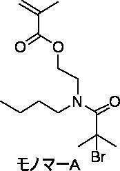
500mLの三口フラスコに、N,N-ジメチルアセトアミド(8.4g)を入れ、窒素気流下、65℃まで加熱した。そこへ、上記で得たモノマーA(7.3g)、t-ブチルアクリレート(20.54g)、V-601(和光純薬製)(0.335g)のN,N-ジメチルアセトアミド(19.5g)溶液を、4時間かけて滴下した。滴下終了後、更に反応溶液を3時間撹拌した。その後、反応溶液にN,N-ジメチルアセトアミド(130g)を足し、室温まで反応溶液を冷却した。上記の反応溶液に4-ヒドロキシTEMPO(東京化成製)(0.04g)およびDBU(16.63g)を加え、室温で12時間反応を行った。その後、反応溶液に70質量%メタンスルホン酸水溶液(16.5g)を加えた。反応終了後、水で再沈を行い、固形物を取り出し、ポリマーC(重量平均分子量6.5万)を15g得た。なお、ポリマー中の各ユニット比は、架橋性基ユニット:極性変換基ユニット=12:88(mol比)であった。
N, N-dimethylacetamide (8.4 g) was placed in a 500 mL three-necked flask and heated to 65 ° C. under a nitrogen stream. Thereto, N, N-dimethylacetamide (19.5 g) of monomer A (7.3 g) obtained above, t-butyl acrylate (20.54 g), V-601 (manufactured by Wako Pure Chemical Industries, Ltd.) (0.335 g). ) The solution was added dropwise over 4 hours. After completion of the dropwise addition, the reaction solution was further stirred for 3 hours. Thereafter, N, N-dimethylacetamide (130 g) was added to the reaction solution, and the reaction solution was cooled to room temperature. 4-Hydroxy TEMPO (manufactured by Tokyo Chemical Industry) (0.04 g) and DBU (16.63 g) were added to the above reaction solution, and reacted at room temperature for 12 hours. Then, 70 mass% methanesulfonic acid aqueous solution (16.5g) was added to the reaction solution. After completion of the reaction, reprecipitation was carried out with water, and the solid matter was taken out to obtain 15 g of polymer C (weight average molecular weight 65,000). In addition, each unit ratio in a polymer was crosslinkable group unit: polar conversion group unit = 12: 88 (mol ratio).
(合成例4:ポリマーD)
500mLの三口フラスコに2-フェニル-2-プロパノール(和光純薬製)(25g)、トリエチルアミン(30g)、テトラヒドロフラン(150mL)を入れて氷浴にて冷却をした。反応溶液の内温10℃以下になるように調節して、そこへ塩化アクリロイル(25g)を滴下した。その後、内温を室温(25℃)まで上昇させて5時間反応させた。反応終了後、酢酸エチル300mL、蒸留水100mL追加した。その後、酢エチ層を飽和重曹水100mLで洗浄後、飽和食塩水100mLで洗浄し、硫酸マグネシウムで乾燥した。その後、酢酸エチルを留去し、カラムクロマトグラフィーにて精製しモノマーB(10g)を得た。 (Synthesis Example 4: Polymer D)
2-phenyl-2-propanol (Wako Pure Chemical Industries, Ltd.) (25 g), triethylamine (30 g), and tetrahydrofuran (150 mL) were placed in a 500 mL three-necked flask and cooled in an ice bath. The inner temperature of the reaction solution was adjusted to 10 ° C. or lower, and acryloyl chloride (25 g) was added dropwise thereto. Thereafter, the internal temperature was raised to room temperature (25 ° C.) and reacted for 5 hours. After completion of the reaction, 300 mL of ethyl acetate and 100 mL of distilled water were added. Thereafter, the ethyl acetate layer was washed with 100 mL of saturated aqueous sodium bicarbonate, then with 100 mL of saturated brine, and dried over magnesium sulfate. Then, ethyl acetate was distilled off and purified by column chromatography to obtain monomer B (10 g).

500mLの3つ口フラスコを窒素置換し、PEGMEA(7.7g)を入れ、65℃に昇温した。その中に、グリシジルメタクリレート(1.0g)、モノマーB(10.0g)、V-601(0.11g)、およびPEGMEA(18.1g)の混合液を4時間かけて滴下した。滴下終了後、4時間反応を行い、ポリマーDの30wt%溶液(37g)を得た。なお、ポリマー中の各ユニット比は、架橋性基ユニット:極性変換基ユニット=12:88(mol比)であった。また、重量平均分子量は、ポリスチレン換算でMw=12.1万(Mw/Mn=4.0)であった。
A 500 mL three-necked flask was purged with nitrogen, PEGMEA (7.7 g) was added, and the temperature was raised to 65 ° C. Into this, a mixture of glycidyl methacrylate (1.0 g), monomer B (10.0 g), V-601 (0.11 g), and PEGMEA (18.1 g) was added dropwise over 4 hours. Reaction was performed after completion | finish of dripping for 4 hours, and the 30 wt% solution (37g) of the polymer D was obtained. In addition, each unit ratio in a polymer was crosslinkable group unit: polar conversion group unit = 12: 88 (mol ratio). Moreover, the weight average molecular weight was Mw = 121,000 (Mw / Mn = 4.0) in terms of polystyrene.
(合成例5:ポリマーE)
500mLの3つ口フラスコを窒素置換し、トルエン(7.8g)を入れ、65℃に昇温した。その中に、グリシジルメタクリレート(1.16g)、アクリル酸1-エチルシクロペンチル(10.0g)、V-601(0.125g)、およびトルエン(18.3g)の混合液を4時間かけて滴下した。滴下終了後、4時間反応を行い、ポリマーEの30wt%溶液(37g)を得た。なお、ポリマー中の各ユニット比は、架橋性基ユニット:極性変換基ユニット=12:88(mol比)であった。また、重量平均分子量は、ポリスチレン換算でMw=5.0万(Mw/Mn=2.6)であった。 (Synthesis Example 5: Polymer E)
A 500 mL three-necked flask was purged with nitrogen, toluene (7.8 g) was added, and the temperature was raised to 65 ° C. A mixture of glycidyl methacrylate (1.16 g), 1-ethylcyclopentyl acrylate (10.0 g), V-601 (0.125 g), and toluene (18.3 g) was added dropwise over 4 hours. . Reaction was performed after completion | finish of dripping for 4 hours, and the 30 wt% solution (37g) of the polymer E was obtained. In addition, each unit ratio in a polymer was crosslinkable group unit: polar conversion group unit = 12: 88 (mol ratio). Moreover, the weight average molecular weight was Mw = 50,000 (Mw / Mn = 2.6) in polystyrene conversion.
(合成例6:ポリマーF)
500mLの三口フラスコに4-メトキシ-α-メチルベンジルアルコール(ALDRICH製)(25g)、トリエチルアミン(26g)、テトラヒドロフラン(150mL)を入れて氷浴にて冷却をした。反応溶液の内温10℃以下になるように調節して、そこへ塩化アクリロイル(22.3g)を滴下した。その後、内温を室温(25℃)まで上昇させて5時間反応させた。反応終了後、酢酸エチル300mL、蒸留水100mLを追加した。その後、酢エチ層を飽和重曹水100mLで洗浄後、飽和食塩水100mLで洗浄し、硫酸マグネシウムで乾燥した。その後、酢酸エチルを留去し、カラムクロマトグラフィーにて精製しモノマーC(20g)を得た。 (Synthesis Example 6: Polymer F)
4-Methoxy-α-methylbenzyl alcohol (ALDRICH) (25 g), triethylamine (26 g), and tetrahydrofuran (150 mL) were placed in a 500 mL three-necked flask and cooled in an ice bath. The inner temperature of the reaction solution was adjusted to 10 ° C. or lower, and acryloyl chloride (22.3 g) was added dropwise thereto. Thereafter, the internal temperature was raised to room temperature (25 ° C.) and reacted for 5 hours. After completion of the reaction, 300 mL of ethyl acetate and 100 mL of distilled water were added. Thereafter, the ethyl acetate layer was washed with 100 mL of saturated aqueous sodium bicarbonate, then with 100 mL of saturated brine, and dried over magnesium sulfate. Thereafter, ethyl acetate was distilled off, and the residue was purified by column chromatography to obtain monomer C (20 g).

500mLの3つ口フラスコを窒素置換し、トルエン(7.7g)を入れ、65℃に昇温した。その中に、グリシジルメタクリレート(0.94g)、モノマーC(10.0g)、V-601(0.19g)、およびトルエン(17.7g)の混合液を4時間かけて滴下した。滴下終了後、4時間反応を行い、ポリマーFの30wt%溶液(36.7g)を得た。なお、ポリマー中の各ユニット比は、架橋性基ユニット:極性変換基ユニット=12:88(mol比)であった。また、重量平均分子量は、ポリスチレン換算でMw=7.6万(Mw/Mn=4.2)であった。
A 500 mL three-necked flask was purged with nitrogen, toluene (7.7 g) was added, and the temperature was raised to 65 ° C. Into this, a mixture of glycidyl methacrylate (0.94 g), monomer C (10.0 g), V-601 (0.19 g), and toluene (17.7 g) was added dropwise over 4 hours. Reaction was performed after completion | finish of dripping for 4 hours, and the 30 wt% solution (36.7g) of the polymer F was obtained. In addition, each unit ratio in a polymer was crosslinkable group unit: polar conversion group unit = 12: 88 (mol ratio). Moreover, the weight average molecular weight was Mw = 76,000 (Mw / Mn = 4.2) in terms of polystyrene.
(合成例7:ポリマーG)
500mLの三口フラスコに、シクロヘキサノール(15g)、ピリジン(12.5g)、アセトニトリル(100mL)を入れて氷浴にて冷却をした。反応溶液の内温10℃以下になるように調節して、そこへアセトニトリル(50mL)に溶かしたp-スチレンスルホニルクロリド(20g)を滴下した。その後、内温を室温(25℃)まで上昇させて5時間反応させた。反応終了後、酢酸エチル300mL、蒸留水100mLを追加した。その後、酢エチ層を飽和重曹水100mLで洗浄後、飽和食塩水100mLで洗浄し、硫酸マグネシウムで乾燥した。その後、酢酸エチルを留去し、カラムクロマトグラフィーにて精製しモノマーD(20g)を得た。 (Synthesis Example 7: Polymer G)
Cyclohexanol (15 g), pyridine (12.5 g), and acetonitrile (100 mL) were placed in a 500 mL three-necked flask and cooled in an ice bath. The inner temperature of the reaction solution was adjusted to 10 ° C. or lower, and p-styrenesulfonyl chloride (20 g) dissolved in acetonitrile (50 mL) was added dropwise thereto. Thereafter, the internal temperature was raised to room temperature (25 ° C.) and reacted for 5 hours. After completion of the reaction, 300 mL of ethyl acetate and 100 mL of distilled water were added. Thereafter, the ethyl acetate layer was washed with 100 mL of saturated aqueous sodium bicarbonate, then with 100 mL of saturated brine, and dried over magnesium sulfate. Then, ethyl acetate was distilled off and purified by column chromatography to obtain monomer D (20 g).
500mLの3つ口フラスコを窒素置換し、PEGMEA(6.3g)を入れ、60℃に昇温した。その中に、グリシジルメタクリレート(1.02g)、t-ブチルアクリレート(6.0g)、モノマーD(1.92g)、V-65(0.11g)、およびPEGMEA(14.6g)の混合液を2時間かけて滴下した。滴下終了後、2時間反応を行い、ポリマーGの30wt%溶液(29.9g)を得た。なお、ポリマー中の各ユニット比は、架橋性基ユニット:t-ブチルアクリレートユニット:モノマーDユニット=12:78:10(mol比)であった。また、重量平均分子量は、ポリスチレン換算でMw=6.6万(Mw/Mn=2.8)であった。
A 500 mL three-necked flask was purged with nitrogen, PEGMEA (6.3 g) was added, and the temperature was raised to 60 ° C. In it, a mixed solution of glycidyl methacrylate (1.02 g), t-butyl acrylate (6.0 g), monomer D (1.92 g), V-65 (0.11 g), and PEGMEA (14.6 g). It was dripped over 2 hours. Reaction was performed after completion | finish of dripping for 2 hours, and the 30 wt% solution (29.9g) of the polymer G was obtained. The unit ratio in the polymer was crosslinkable group unit: t-butyl acrylate unit: monomer D unit = 12: 78: 10 (mol ratio). Moreover, the weight average molecular weight was Mw = 66,000 (Mw / Mn = 2.8) in polystyrene conversion.
(合成例8:ポリマーH)
500mLの三口フラスコに、アクリル酸(6.08g)、10-カンファースルホン酸(3mg)、ヘキサン(100mL)を入れた。反応溶液の内温30℃以下になるように調節して、そこへオクタデシルビニルエーテル(25g)を滴下した。その後、室温(25℃)で3時間反応させた。反応終了後、商品名キョーワード1000(協和化学工業株式会社製)、商品名キョーワード200(協和化学工業株式会社製)を用いて吸着処理を行い、ヘキサンを減圧留去し、モノマーE(30g)を得た。 (Synthesis Example 8: Polymer H)
A 500 mL three-necked flask was charged with acrylic acid (6.08 g), 10-camphorsulfonic acid (3 mg), and hexane (100 mL). The internal temperature of the reaction solution was adjusted to 30 ° C. or lower, and octadecyl vinyl ether (25 g) was added dropwise thereto. Then, it was made to react at room temperature (25 degreeC) for 3 hours. After completion of the reaction, adsorption treatment was carried out using the product name KYOWARD 1000 (manufactured by Kyowa Chemical Industry Co., Ltd.) and the product name KYOWARD 200 (manufactured by Kyowa Chemical Industry Co., Ltd.). )
500mLの3つ口フラスコを窒素置換し、PEGMEA(6.3g)を入れ、70℃に昇温した。その中に、グリシジルメタクリレート(0.53g)、モノマーE(10.0g)、V-601(0.11g)、およびPEGMEA(11.6g)の混合液を2時間かけて滴下した。滴下終了後、3時間反応を行い、アセトニトリルで再沈を行い、固形物を取り出し、ポリマーH(7g)を得た。なお、ポリマー中の各ユニット比は、架橋性基ユニット:極性変換基ユニット=12:88(mol比)であった。また、重量平均分子量は、ポリスチレン換算でMw=5.0万(Mw/Mn=2.7)であった。
A 500 mL three-necked flask was purged with nitrogen, PEGMEA (6.3 g) was added, and the temperature was raised to 70 ° C. Into this, a mixture of glycidyl methacrylate (0.53 g), monomer E (10.0 g), V-601 (0.11 g), and PEGMEA (11.6 g) was added dropwise over 2 hours. After completion of the dropwise addition, the reaction was performed for 3 hours, reprecipitation was performed with acetonitrile, the solid matter was taken out, and polymer H (7 g) was obtained. In addition, each unit ratio in a polymer was crosslinkable group unit: polar conversion group unit = 12: 88 (mol ratio). Moreover, the weight average molecular weight was Mw = 50,000 (Mw / Mn = 2.7) in polystyrene conversion.
(合成例9:ポリマーI)
500mLの三口フラスコにN-ヒドロキシフタルイミド(15g)、ピリジン(8.7g)、アセトニトリル(100mL)を入れて氷浴にて冷却をした。反応溶液の内温10℃以下になるように調節して、そこへアセトニトリル(50mL)に溶かしたp-スチレンスルホニルクロリド(20g)を滴下した。その後、内温を室温(25℃)まで上昇させて5時間反応させた。反応終了後、酢酸エチル300mL、蒸留水100mLを追加した。その後、酢エチ層を飽和重曹水100mLで洗浄後、飽和食塩水100mLで洗浄し、硫酸マグネシウムで乾燥した。その後、酢酸エチルを留去し、カラムクロマトグラフィーにて精製しモノマーFを22g得た。 (Synthesis Example 9: Polymer I)
N-hydroxyphthalimide (15 g), pyridine (8.7 g), and acetonitrile (100 mL) were placed in a 500 mL three-necked flask and cooled in an ice bath. The inner temperature of the reaction solution was adjusted to 10 ° C. or lower, and p-styrenesulfonyl chloride (20 g) dissolved in acetonitrile (50 mL) was added dropwise thereto. Thereafter, the internal temperature was raised to room temperature (25 ° C.) and reacted for 5 hours. After completion of the reaction, 300 mL of ethyl acetate and 100 mL of distilled water were added. Thereafter, the ethyl acetate layer was washed with 100 mL of saturated aqueous sodium bicarbonate, then with 100 mL of saturated brine, and dried over magnesium sulfate. Then, ethyl acetate was distilled off and purified by column chromatography to obtain 22 g of monomer F.
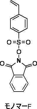
500mLの3つ口フラスコを窒素置換し、PEGMEA(6.3g)を入れ、60℃に昇温した。その中に、グリシジルメタクリレート(1.02g)、t-ブチルアクリレート(6.0g)、モノマーF(1.98g)、V-65(0.11g)、およびPEGMEA(14.6g)の混合液を4時間かけて滴下した。滴下終了後、3時間反応を行い、ポリマーIの30wt%溶液(30g)を得た。なお、ポリマー中の各ユニット比は、架橋性基ユニット:t-ブチルアクリレートユニット:モノマーFユニット=12:78:10(mol比)であった。また、重量平均分子量は、ポリスチレン換算でMw=7.6万(Mw/Mn=3.1)であった。
A 500 mL three-necked flask was purged with nitrogen, PEGMEA (6.3 g) was added, and the temperature was raised to 60 ° C. In it, a mixed solution of glycidyl methacrylate (1.02 g), t-butyl acrylate (6.0 g), monomer F (1.98 g), V-65 (0.11 g), and PEGMEA (14.6 g) was added. It was dripped over 4 hours. Reaction was performed after completion | finish of dripping for 3 hours, and the 30 wt% solution (30g) of the polymer I was obtained. The unit ratio in the polymer was crosslinkable group unit: t-butyl acrylate unit: monomer F unit = 12: 78: 10 (mol ratio). Moreover, the weight average molecular weight was Mw = 76,000 (Mw / Mn = 3.1) in polystyrene conversion.
(合成例10:ポリマーJ)
500mLの3つ口フラスコを窒素置換し、PEGMEA(30g)、t-ブチルアクリレート(12.8g)、およびV-601(0.35g)を入れ、60℃に昇温し、5時間反応させ、ポリマーJの30wt%溶液(43g)を得た。重量平均分子量は、ポリスチレン換算でMw=8.0万(Mw/Mn=2.1)であった。 (Synthesis Example 10: Polymer J)
A 500 mL three-necked flask was purged with nitrogen and charged with PEGMEA (30 g), t-butyl acrylate (12.8 g), and V-601 (0.35 g), heated to 60 ° C., reacted for 5 hours, A 30 wt% solution of polymer J (43 g) was obtained. The weight average molecular weight was Mw = 80,000 (Mw / Mn = 2.1) in terms of polystyrene.
(合成例11:ポリマーK)
500mLの3つ口フラスコを窒素置換し、PEGMEA(33.3g)を入れ、70℃に昇温した。その中に、メタクリル酸3-(トリメトキシシリル)プロピル(5.96g)、t-ブチルアクリレート(22.56g)、V-601(0.69g)、およびPEGMEA(33.3g)の混合液を2時間かけて滴下した。滴下終了後、3時間反応を行い、ポリマーKの30wt%溶液(95g)を得た。なお、ポリマー中の各ユニット比は、架橋性基ユニット:極性変換基ユニット=12:88(mol比)であった。また、重量平均分子量は、ポリスチレン換算でMw=9.2万(Mw/Mn=5.2)であった。 (Synthesis Example 11: Polymer K)
A 500 mL three-necked flask was purged with nitrogen, PEGMEA (33.3 g) was added, and the temperature was raised to 70 ° C. In it, a mixed solution of 3- (trimethoxysilyl) propyl methacrylate (5.96 g), t-butyl acrylate (22.56 g), V-601 (0.69 g), and PEGMEA (33.3 g) was added. It was dripped over 2 hours. Reaction was performed after completion | finish of dripping for 3 hours, and the 30 wt% solution (95g) of the polymer K was obtained. In addition, each unit ratio in a polymer was crosslinkable group unit: polar conversion group unit = 12: 88 (mol ratio). Moreover, the weight average molecular weight was Mw = 92,000 (Mw / Mn = 5.2) in terms of polystyrene.
(合成例12:ポリマーL)
500mLの3つ口フラスコを窒素置換し、PEGMEA(17.7g)を入れ、60℃に昇温した。その中に、ヒドロキシルエチルアクリレート(2.79g)、t-ブチルアクリレート(22.56g)、V-601(0.69g)、およびPEGMEA(41.4g)の混合液を2時間かけて滴下した。滴下終了後、3時間反応を行い、ポリマーLの30wt%溶液(84.5g)を得た。なお、ポリマー中の各ユニット比は、架橋性基ユニット:極性変換基ユニット=12:88(mol比)であった。また、重量平均分子量は、ポリスチレン換算でMw=17.5万(Mw/Mn=3.7)であった。 (Synthesis Example 12: Polymer L)
A 500 mL three-necked flask was purged with nitrogen, PEGMEA (17.7 g) was added, and the temperature was raised to 60 ° C. Into this, a mixture of hydroxylethyl acrylate (2.79 g), t-butyl acrylate (22.56 g), V-601 (0.69 g), and PEGMEA (41.4 g) was added dropwise over 2 hours. Reaction was performed after completion | finish of dripping for 3 hours, and the 30 wt% solution (84.5g) of the polymer L was obtained. In addition, each unit ratio in a polymer was crosslinkable group unit: polar conversion group unit = 12: 88 (mol ratio). Moreover, the weight average molecular weight was Mw = 175,000 (Mw / Mn = 3.7) in terms of polystyrene.
(合成例13:ポリマーM)
500mLの3つ口フラスコを窒素置換し、PEGMEA(30.3g)を入れ、70℃に昇温した。その中に、ジメチルアミノエチルメタリレート(3.44g)、t-ブチルアクリレート(22.56g)、V-601(0.69g)、およびPEGMEA(30.3g)の混合液を2時間かけて滴下した。滴下終了後、3時間反応を行い、ポリマーMの30wt%溶液(86.7g)を得た。なお、ポリマー中の各ユニット比は、架橋性基ユニット:極性変換基ユニット=12:88(mol比)であった。また、重量平均分子量は、ポリスチレン換算でMw=13万(Mw/Mn=3.9)であった。 (Synthesis Example 13: Polymer M)
A 500 mL three-necked flask was purged with nitrogen, PEGMEA (30.3 g) was added, and the temperature was raised to 70 ° C. A mixed solution of dimethylaminoethyl metallate (3.44 g), t-butyl acrylate (22.56 g), V-601 (0.69 g), and PEGMEA (30.3 g) was added dropwise over 2 hours. did. Reaction was performed after completion | finish of dripping for 3 hours, and the 30 wt% solution (86.7g) of the polymer M was obtained. In addition, each unit ratio in a polymer was crosslinkable group unit: polar conversion group unit = 12: 88 (mol ratio). Moreover, the weight average molecular weight was Mw = 130,000 (Mw / Mn = 3.9) in polystyrene conversion.
(合成例14:ポリマーN)
500mLの3つ口フラスコを窒素置換し、PEGMEA(14.1g)を入れ、60℃に昇温した。その中に、OXE-30(大阪有機化学工業製)(2.78g)、t-ブチルアクリレート(17.4g)、V-601(0.277g)、およびPEGMEA(33g)の混合液を4時間かけて滴下した。滴下終了後、3時間反応を行い、ポリマーNの30wt%溶液(67.2g)を得た。なお、ポリマー中の各ユニット比は、架橋性基ユニット:極性変換基ユニット=10:90(mol比)であった。また、重量平均分子量は、ポリスチレン換算でMw=9.2万(Mw/Mn=3.5)であった。 (Synthesis Example 14: Polymer N)
A 500 mL three-necked flask was purged with nitrogen, PEGMEA (14.1 g) was added, and the temperature was raised to 60 ° C. A mixed solution of OXE-30 (manufactured by Osaka Organic Chemical Industry) (2.78 g), t-butyl acrylate (17.4 g), V-601 (0.277 g), and PEGMEA (33 g) was added for 4 hours. It was dripped over. Reaction was performed after completion | finish of dripping for 3 hours, and the 30 wt% solution (67.2g) of the polymer N was obtained. In addition, each unit ratio in a polymer was crosslinkable group unit: polar conversion group unit = 10: 90 (mol ratio). Moreover, the weight average molecular weight was Mw = 92,000 (Mw / Mn = 3.5) in terms of polystyrene.
(合成例15:ポリマーO)
500mLの3つ口フラスコを窒素置換し、PEGMEA(23.7g)を入れ、60℃に昇温した。その中に、グリシジルメタクリレート(17.7g)、t-ブチルアクリレート(16.3g)、V-601(0.46g)、およびPEGMEA(55.2g)の混合液を4時間かけて滴下した。滴下終了後、3時間反応を行い、ポリマーOの30wt%溶液(113g)を得た。なお、ポリマー中の各ユニット比は、架橋性基ユニット:極性変換基ユニット=50:50(mol比)であった。また、重量平均分子量は、ポリスチレン換算でMw=9.1万(Mw/Mn=4.1)であった。 (Synthesis Example 15: Polymer O)
A 500 mL three-necked flask was purged with nitrogen, PEGMEA (23.7 g) was added, and the temperature was raised to 60 ° C. Into this, a mixture of glycidyl methacrylate (17.7 g), t-butyl acrylate (16.3 g), V-601 (0.46 g), and PEGMEA (55.2 g) was added dropwise over 4 hours. Reaction was performed after completion | finish of dripping for 3 hours, and the 30 wt% solution (113g) of the polymer O was obtained. In addition, each unit ratio in a polymer was crosslinkable group unit: polar conversion group unit = 50: 50 (mol ratio). Moreover, the weight average molecular weight was Mw = 91,000 (Mw / Mn = 4.1) in terms of polystyrene.
(合成例16:ポリマーP)
500mLの3つ口フラスコを窒素置換し、PEGMEA(10.7g)を入れ、55℃に昇温した。その中に、グリシジルメタクリレート(0.85g)、モノマーD(14.4g)、V-65(0.11g)、およびPEGMEA(24.9g)の混合液を2時間かけて滴下した。滴下終了後、3時間反応を行い、ポリマーPの30wt%溶液(50.8g)を得た。なお、ポリマー中の各ユニット比は、架橋性基ユニット:モノマーDユニット=10:90(mol比)であった。また、重量平均分子量は、ポリスチレン換算でMw=8.6万(Mw/Mn=3.8)であった。 (Synthesis Example 16: Polymer P)
A 500 mL three-necked flask was purged with nitrogen, PEGMEA (10.7 g) was added, and the temperature was raised to 55 ° C. Into this, a mixture of glycidyl methacrylate (0.85 g), monomer D (14.4 g), V-65 (0.11 g), and PEGMEA (24.9 g) was added dropwise over 2 hours. Reaction was performed after completion | finish of dripping for 3 hours, and the 30 wt% solution (50.8g) of the polymer P was obtained. In addition, each unit ratio in a polymer was crosslinkable group unit: monomer D unit = 10: 90 (mol ratio). Moreover, the weight average molecular weight was Mw = 86,000 (Mw / Mn = 3.8) in terms of polystyrene.
(合成例17:ポリマーQ)
500mLの三口フラスコに、アクリル酸(17.99g)、10-カンファースルホン酸(6mg)、ヘキサン(100mL)を入れた。反応溶液の内温30℃以下になるように調節して、そこへイソブチルビニルエーテル(25g)を滴下した。その後、室温(25℃)で3時間反応させた。反応終了後、商品名キョーワード1000(協和化学工業株式会社製)、商品名キョーワード200(協和化学工業株式会社製)を用いて吸着処理を行い、ヘキサンを減圧留去し、モノマーG(42g)を得た。 (Synthesis Example 17: Polymer Q)
A 500 mL three-necked flask was charged with acrylic acid (17.99 g), 10-camphorsulfonic acid (6 mg), and hexane (100 mL). The internal temperature of the reaction solution was adjusted to 30 ° C. or lower, and isobutyl vinyl ether (25 g) was added dropwise thereto. Then, it was made to react at room temperature (25 degreeC) for 3 hours. After completion of the reaction, adsorption treatment was performed using trade name Kyoward 1000 (manufactured by Kyowa Chemical Industry Co., Ltd.) and trade name Kyoword 200 (manufactured by Kyowa Chemical Industry Co., Ltd.), and hexane was distilled off under reduced pressure to give monomer G (42 g )

500mLの3つ口フラスコを窒素置換し、PEGMEA(4.6g)を入れ、70℃に昇温した。その中に、グリシジルメタクリレート(1.02g)、モノマーG(9.1g)、V-601(0.208g)、およびPEGMEA(11.5g)の混合液を2時間かけて滴下した。滴下終了後、3時間反応を行い、アセトニトリルで再沈を行い、固形物を取り出し、ポリマーQ(6g)を得た。なお、ポリマー中の各ユニット比は、架橋性基ユニット:極性変換基ユニット=12:88(mol比)であった。また、重量平均分子量は、ポリスチレン換算でMw=6.2万(Mw/Mn=2.9)であった。
A 500 mL three-necked flask was purged with nitrogen, PEGMEA (4.6 g) was added, and the temperature was raised to 70 ° C. Into this, a mixture of glycidyl methacrylate (1.02 g), monomer G (9.1 g), V-601 (0.208 g), and PEGMEA (11.5 g) was added dropwise over 2 hours. After completion of the dropwise addition, the reaction was performed for 3 hours, reprecipitation was performed with acetonitrile, the solid matter was taken out, and polymer Q (6 g) was obtained. In addition, each unit ratio in a polymer was crosslinkable group unit: polar conversion group unit = 12: 88 (mol ratio). Moreover, the weight average molecular weight was Mw = 62,000 (Mw / Mn = 2.9) in polystyrene conversion.
(合成例18:ポリマーR)
500mLの3つ口フラスコを窒素置換し、PEGMEA(6.5g)を入れ、60℃に昇温した。その中に、グリシジルメタクリレート(0.43g)、モノマーF(8.89g)、V-65(0.055g)、およびPEGMEA(15.2g)の混合液を4時間かけて滴下した。滴下終了後、3時間反応を行い、ポリマーRの30wt%溶液(30g)を得た。なお、ポリマー中の各ユニット比は、架橋性基ユニット:モノマーFユニット=10:90(mol比)であった。また、重量平均分子量は、ポリスチレン換算でMw=7.2万(Mw/Mn=3.0)であった。 (Synthesis Example 18: Polymer R)
A 500 mL three-necked flask was purged with nitrogen, PEGMEA (6.5 g) was added, and the temperature was raised to 60 ° C. Into this, a mixture of glycidyl methacrylate (0.43 g), monomer F (8.89 g), V-65 (0.055 g), and PEGMEA (15.2 g) was added dropwise over 4 hours. Reaction was performed after completion | finish of dripping for 3 hours, and the 30 wt% solution (30g) of the polymer R was obtained. In addition, each unit ratio in a polymer was crosslinkable group unit: monomer F unit = 10: 90 (mol ratio). Moreover, the weight average molecular weight was Mw = 72,000 (Mw / Mn = 3.0) in polystyrene conversion.
(合成例19:比較ポリマー1)
500mLの三口フラスコに、N,N-ジメチルアセトアミド(13.8g)を入れ、窒素気流下、65℃まで加熱した。そこへ、モノマーA(11.53g)、アクリル酸(8.21g)、V-601(和光純薬製)(0.276g)のN,N-ジメチルアセトアミド溶液(32.2g)を、4時間かけて滴下した。滴下終了後、更に3時間撹拌した。その後、N,N-ジメチルアセトアミド(154g)を足し、室温まで反応溶液を冷却した。上記の反応溶液に、4-ヒドロキシTEMPO(東京化成製)(0.06g)、DBU(58g)を加え、室温で12時間反応を行った。その後、反応溶液に70質量%メタンスルホン酸水溶液(55g)を加えた。反応終了後、水で再沈を行い、固形物を取り出し比較ポリマー1(15g)を得た。なお、ポリマー中の各ユニット比は、架橋性基ユニット:アクリル酸ユニット=24:76(mol比)であった。また、重量平均分子量は、ポリスチレン換算でMw=5.2万(Mw/Mn=2.2)であった。
なお、該比較ポリマー1中には、極性変換基が含まれない。 (Synthesis Example 19: Comparative polymer 1)
N, N-dimethylacetamide (13.8 g) was placed in a 500 mL three-necked flask and heated to 65 ° C. under a nitrogen stream. Thereto, N, N-dimethylacetamide solution (32.2 g) of monomer A (11.53 g), acrylic acid (8.21 g), V-601 (manufactured by Wako Pure Chemical Industries, Ltd.) (0.276 g) was added for 4 hours. It was dripped over. After completion of dropping, the mixture was further stirred for 3 hours. Thereafter, N, N-dimethylacetamide (154 g) was added, and the reaction solution was cooled to room temperature. 4-hydroxy TEMPO (manufactured by Tokyo Chemical Industry) (0.06 g) and DBU (58 g) were added to the above reaction solution, and the reaction was carried out at room temperature for 12 hours. Then, 70 mass% methanesulfonic acid aqueous solution (55g) was added to the reaction solution. After completion of the reaction, reprecipitation was performed with water, and the solid matter was taken out to obtain comparative polymer 1 (15 g). In addition, each unit ratio in a polymer was crosslinkable group unit: acrylic acid unit = 24: 76 (mol ratio). Moreover, the weight average molecular weight was Mw = 52,000 (Mw / Mn = 2.2) in terms of polystyrene.
The comparative polymer 1 does not contain a polarity converting group.
(合成例20:比較ポリマー2)
500mLの3つ口フラスコを窒素置換し、PEGMEA(10g)を入れ、60℃に昇温した。その中に、グリシジルメタクリレート(1.71g)、メタクリル酸イソブチル(12.51g)、V-601(0.184g)、およびPEGMEA(23.2g)の混合液を4時間かけて滴下した。滴下終了後、4時間反応を行い、比較ポリマー2の30wt%溶液(47.6g)を得た。なお、ポリマー中の各ユニット比は、架橋性基ユニット:メタクリル酸イソブチルユニット=12:88(mol比)であった。また、重量平均分子量はポリスチレン換算でMw=8.8万(Mw/Mn=3.5)であった。
なお、該比較ポリマー2中には、極性変換基が含まれない。 (Synthesis Example 20: Comparative polymer 2)
A 500 mL three-necked flask was purged with nitrogen, PEGMEA (10 g) was added, and the temperature was raised to 60 ° C. Into this, a mixture of glycidyl methacrylate (1.71 g), isobutyl methacrylate (12.51 g), V-601 (0.184 g), and PEGMEA (23.2 g) was added dropwise over 4 hours. Reaction was performed after completion | finish of dripping for 4 hours, and the 30 wt% solution (47.6g) of the comparison polymer 2 was obtained. In addition, each unit ratio in a polymer was crosslinkable group unit: isobutyl methacrylate unit = 12: 88 (mol ratio). Moreover, the weight average molecular weight was Mw = 88,000 (Mw / Mn = 3.5) in terms of polystyrene.
The comparative polymer 2 does not contain a polarity converting group.
(合成例21:比較ポリマー3)
500mLの三口フラスコに、N,N-ジメチルアセトアミド(9.4g)を入れ、窒素気流下、65℃まで加熱した。そこへ、2-ヒドロキシエチルアクリレート(東京化成製)(5.8g)、アクリロニトリル(東京化成工業(株)製)(3.8g)、アクリル酸(東京化成工業(株)製)(9.0g)、V-65(和光純薬工業(株)製)(0.5g)のN,N-ジメチルアセトアミド(9.4g)溶液を、4時間かけて滴下した。滴下終了後、更に3時間撹拌した。その後、N,N-ジメチルアセトアミド(56g)をたし、室温まで反応溶液を冷却した。上記の反応溶液に、カレンズMO(I7.6g)、U-600(日東化成製)(0.2g)、TEMPO(東京化成工業(株)製)(0.08g)を加え、45℃に加熱し6時間反応させた。その後、メタノール(1.6g)を加え1.5時間反応させ反応を終了した。反応終了後、水で再沈を行い、固形物を取り出し、比較ポリマー3(14g)を得た。なお、ポリマー中の各ユニット比は、架橋性基ユニット:アクリロニトリルユニット:アクリル酸ユニット=20:30:50(mol比)であった。また、重量平均分子量は、ポリスチレン換算でMw=4.2(Mw/Mn=2.2)であった。
なお、該比較ポリマー3は、特許文献1で使用されているポリマーであり、極性変換基が含まれない。 (Synthesis Example 21: Comparative polymer 3)
N, N-dimethylacetamide (9.4 g) was placed in a 500 mL three-necked flask and heated to 65 ° C. under a nitrogen stream. There, 2-hydroxyethyl acrylate (manufactured by Tokyo Chemical Industry) (5.8 g), acrylonitrile (manufactured by Tokyo Chemical Industry Co., Ltd.) (3.8 g), acrylic acid (manufactured by Tokyo Chemical Industry Co., Ltd.) (9.0 g) ), A solution of V-65 (manufactured by Wako Pure Chemical Industries, Ltd.) (0.5 g) in N, N-dimethylacetamide (9.4 g) was added dropwise over 4 hours. After completion of dropping, the mixture was further stirred for 3 hours. Thereafter, N, N-dimethylacetamide (56 g) was added, and the reaction solution was cooled to room temperature. To the above reaction solution, Karenz MO (I 7.6 g), U-600 (manufactured by Nitto Kasei) (0.2 g), TEMPO (manufactured by Tokyo Chemical Industry Co., Ltd.) (0.08 g) was added and heated to 45 ° C. And allowed to react for 6 hours. Thereafter, methanol (1.6 g) was added and reacted for 1.5 hours to complete the reaction. After completion of the reaction, reprecipitation was performed with water, and the solid matter was taken out to obtain comparative polymer 3 (14 g). In addition, each unit ratio in a polymer was crosslinkable group unit: acrylonitrile unit: acrylic acid unit = 20: 30: 50 (mol ratio). Moreover, the weight average molecular weight was Mw = 4.2 (Mw / Mn = 2.2) in terms of polystyrene.
The comparative polymer 3 is a polymer used in Patent Document 1 and does not contain a polarity converting group.
(合成例22:比較ポリマー4)
1000mlの三口フラスコに、N,N-ジメチルアセトアミド(35g)を入れ、窒素気流下、75℃まで加熱した。そこへ、2-ヒドロキシエチルアクリレート(市販品、東京化成製)(6.60g)、2-シアノエチルアクリレート(28.4g)、V-601(和光純薬製)(0.65g)のN,N-ジメチルアセトアミド(35g)溶液を、2.5時間かけて滴下した。滴下終了後、80℃まで加熱し、更に3時間撹拌した。その後、室温まで、反応溶液を冷却した。
上記の反応溶液に、ジターシャリーブチルハイドロキノン(0.29g)、ジブチルチンジラウレート(0.29g)、カレンズAOI(昭和電工(株)製)(18.56g)、N,N-ジメチルアセトアミド(19g)を加え、55℃で4時間反応を行った。その後、反応液にメタノール(3.6g)を加え、更に1.5時間反応を行った。反応終了後、酢酸エチル:ヘキサン=1:1で再沈を行い、固形物を取り出し、比較ポリマー4(重量平均分子量6.2万)(32g)を得た。なお、ポリマー中の各ユニット比は、架橋性基ユニット:シアノ基ユニット=20:80(mol比)であった。また、重量平均分子量はポリスチレン換算でMw=6.2(Mw/Mn=2.3)であった。
なお、該比較ポリマー4中には、極性変換基が含まれない。 (Synthesis Example 22: Comparative polymer 4)
N, N-dimethylacetamide (35 g) was placed in a 1000 ml three-necked flask and heated to 75 ° C. under a nitrogen stream. There, N, N of 2-hydroxyethyl acrylate (commercial product, manufactured by Tokyo Chemical Industry) (6.60 g), 2-cyanoethyl acrylate (28.4 g), V-601 (manufactured by Wako Pure Chemical Industries) (0.65 g) -A solution of dimethylacetamide (35 g) was added dropwise over 2.5 hours. After completion of dropping, the mixture was heated to 80 ° C. and further stirred for 3 hours. Thereafter, the reaction solution was cooled to room temperature.
Ditertiary butyl hydroquinone (0.29 g), dibutyltin dilaurate (0.29 g), Karenz AOI (manufactured by Showa Denko KK) (18.56 g), N, N-dimethylacetamide (19 g) And reacted at 55 ° C. for 4 hours. Thereafter, methanol (3.6 g) was added to the reaction solution, and the reaction was further performed for 1.5 hours. After completion of the reaction, reprecipitation was performed with ethyl acetate: hexane = 1: 1, and the solid matter was taken out to obtain comparative polymer 4 (weight average molecular weight 62,000) (32 g). In addition, each unit ratio in a polymer was crosslinkable group unit: cyano group unit = 20: 80 (mol ratio). Moreover, the weight average molecular weight was Mw = 6.2 (Mw / Mn = 2.3) in terms of polystyrene.
The comparative polymer 4 does not contain a polarity converting group.
上記合成例1~22で合成した各種ポリマーの構造式を以下にまとめて示す。なお、下記に示すポリマー中の繰り返し単位に併記された数値は重合モル比を示す。
The structural formulas of the various polymers synthesized in Synthesis Examples 1 to 22 are summarized below. In addition, the numerical value written together with the repeating unit in the polymer shown below shows superposition | polymerization molar ratio.
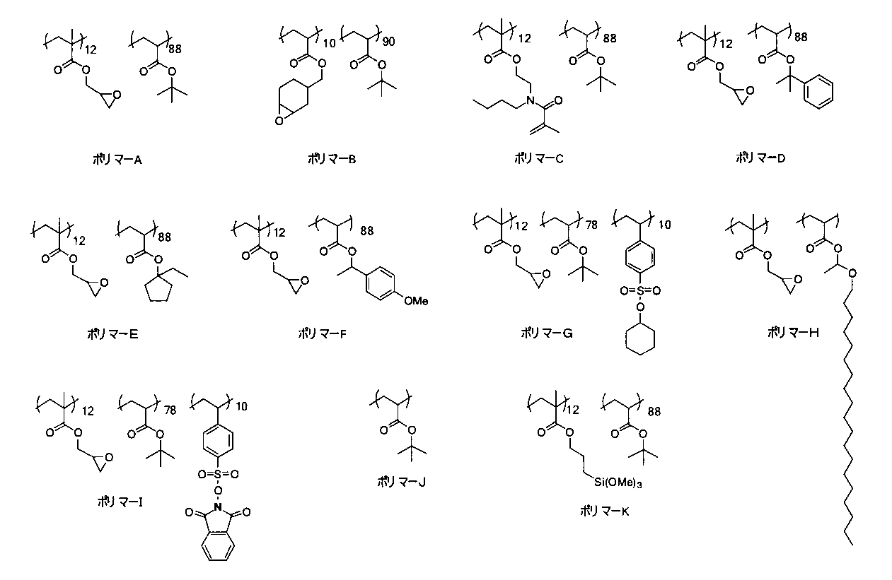


<実施例1>
(工程(H)および(A))
厚さ18μmの銅膜を片面に有する基板の銅膜面側に、味の素ファインテクノ社製エポキシ系絶縁膜GX-13(膜厚40μm)を、真空ラミネーターにより0.2MPaの圧力で100~110℃の条件により接着し、基板上に絶縁層を形成した。 <Example 1>
(Process (H) and (A))
An epoxy insulating film GX-13 (film thickness: 40 μm) manufactured by Ajinomoto Fine Techno Co., Ltd. is applied to the copper film side of a substrate having a copper film having a thickness of 18 μm on one side and a pressure of 0.2 MPa by a vacuum laminator at 100 to 110 ° C. The insulating layer was formed on the substrate by bonding under the above conditions.
(被めっき層の形成)
上記で得られたポリマーAの30wt%溶液(3g)、プロピレングリコールモノメチルエーテル(以下、MFGと略す)(7g)を混合攪拌し、被めっき層形成用組成物を調製した。
調製された被めっき層形成用組成物を、被めっき層の厚さが1μmになるように、絶縁層上にスピンコート法により塗布し、150℃で20分間乾燥、硬化し、被めっき層を形成した。
得られた被めっき層の水に対する接触角を、接触角測定装置(協和界面科学社製、型式:DM500)を用いて測定したところ、89°であり、疎水性であった。 (Formation of plated layer)
A 30 wt% solution (3 g) of polymer A obtained above and propylene glycol monomethyl ether (hereinafter abbreviated as MFG) (7 g) were mixed and stirred to prepare a composition for forming a layer to be plated.
The prepared composition for forming a layer to be plated is applied onto the insulating layer by spin coating so that the thickness of the layer to be plated becomes 1 μm, dried and cured at 150 ° C. for 20 minutes, and the layer to be plated is formed. Formed.
When the contact angle with respect to the water of the obtained to-be-plated layer was measured using the contact angle measuring apparatus (the Kyowa Interface Science company make, model: DM500), it was 89 degrees and was hydrophobic.
(工程(B))
工程(A)で得られた被めっき層付き基板に対して、CO2レーザにより、被めっき層および絶縁層を貫通し、銅膜表面まで到達する、トップ径60μm、ボトム径50μmのビアホールを形成した。 (Process (B))
A via hole having a top diameter of 60 μm and a bottom diameter of 50 μm is formed on the substrate with the layer to be plated obtained in the step (A) by a CO 2 laser to reach the copper film surface through the layer to be plated and the insulating layer. did.
(工程(C))
続いて、ビアホールが形成された面に対しデスミア処理を行った。
具体的には、以下のコンディショナー水溶液を調製し、該水溶液を攪拌しながら、工程(B)で得られた基板を該水溶液に60℃にて10分間浸漬処理することで、被めっき層表面に膨潤処理を行った。次に、コンディショナー水溶液より基板を取り出し、50℃温水にて3分処理した。次に、デスミア液(アルカリ性過マンガン水溶液:pH=13.5)に攪拌を加えながら、温水処理された基板を該デスミア液に80℃にて30分間浸漬することでデスミア処理を行った。
その後、デスミア処理された基板を50℃温水にて3分浸漬処理した。
使用したコンディショナー液、デスミア液の液組成を以下に示す。 (Process (C))
Subsequently, desmear treatment was performed on the surface on which the via hole was formed.
Specifically, the following conditioner aqueous solution was prepared, and the substrate obtained in the step (B) was immersed in the aqueous solution at 60 ° C. for 10 minutes while stirring the aqueous solution. Swelling treatment was performed. Next, the substrate was taken out from the conditioner aqueous solution and treated with warm water at 50 ° C. for 3 minutes. Next, the desmear treatment was performed by immersing the hot-water treated substrate in the desmear solution at 80 ° C. for 30 minutes while stirring the desmear solution (alkaline permanganese aqueous solution: pH = 13.5).
Thereafter, the desmeared substrate was immersed in hot water at 50 ° C. for 3 minutes.
The liquid composition of the used conditioner liquid and desmear liquid is shown below.
(コンディショナー水溶液)
・蒸留水 49g
・スウェリングディップセキュリガンドP(アトテック・ジャパン(株)製) 51g
・水酸化ナトリウム(和光純薬特級) 0.3g
(デスミア液)
・蒸留水 42g
・コンセントレート・コンパクトCP(アトテック・ジャパン(株)製) 62g
・水酸化ナトリウム(和光純薬特級) 4g
デスミア処理後の被めっき層の表面粗さRaを、JIS B0601(2001)に基づき、AFM(S-image,エスアイアイ・ナノテクノロジー(株)製)を用いて測定した結果、Ra=0.05μmであった。 (Conditioner aqueous solution)
・ Distilled water 49g
・ Swelling Dip Securigand P (Atotech Japan Co., Ltd.) 51g
・ Sodium hydroxide (Wako Pure Chemical) 0.3g
(Desmear liquid)
・ 42g distilled water
・ Concentrate Compact CP (Atotech Japan Co., Ltd.) 62g
・ Sodium hydroxide (Wako Pure Chemical) 4g
As a result of measuring the surface roughness Ra of the plated layer after the desmear treatment using AFM (S-image, manufactured by SII Nano Technology Co., Ltd.) based on JIS B0601 (2001), Ra = 0.05 μm Met.
(工程(D))
工程(C)で得られた基板を、硫酸ヒドロキシルアミン1.5wt%と硫酸40wt%を含む水溶液からなる酸処理水溶液(液温:90℃)中に、攪拌を加えながら30分間浸漬し、親水化処理を行なった。その後、基板を酸処理水溶液から取り出し、50℃温水にて3分浸漬処理を行なった。 (Process (D))
The substrate obtained in step (C), hydroxylamine 1.5 wt% and the acid treatment solution comprising an aqueous solution containing sulfuric acid 40 wt% (liquid temperature: 90 ° C.) sulfate in, were immersed while applying stirring for 30 min, a hydrophilic The treatment was performed. Thereafter, the substrate was taken out from the acid-treated aqueous solution and immersed in hot water at 50 ° C. for 3 minutes.
ATR-赤外分光光度計を用いて酸処理後の被めっき層のIRスペクトルを測定したところ、1367cm-1の極性変換基(三級エステル基)由来のピークが消失していることが確認され、新たに1710cm-1にカルボン酸基由来のピークが確認された。すなわち極性変換基が親水性基(カルボン酸基)へと変換していることが確認された。また酸処理後の被めっき層の水に対する接触角を、接触角測定装置(協和界面科学社製、型式:DM500)を用いて測定したところ39°であり、被めっき層の接触角が低下していることが確認された。
When the IR spectrum of the plated layer after acid treatment was measured using an ATR-infrared spectrophotometer, it was confirmed that the peak derived from the polar conversion group (tertiary ester group) at 1367 cm −1 disappeared. A new peak derived from a carboxylic acid group was confirmed at 1710 cm −1 . That is, it was confirmed that the polar conversion group was converted to a hydrophilic group (carboxylic acid group). Moreover, when the contact angle with respect to the water of the to-be-plated layer after an acid treatment was measured using the contact angle measuring apparatus (Kyowa Interface Science company make, model: DM500), it was 39 degrees, and the contact angle of the to-be-plated layer fell. It was confirmed that
(工程(E))
工程(D)で得られた基板を、スルカップACL-009(上村工業株式会社製)の5wt%水溶液(液温:50℃)に5分間浸漬し、浸漬後に純水にて2回洗浄した。その後、上記処理が施された基板を、Pd触媒付与液であるアクチベーターネオガント834(アトテックジャパン社製)に室温にて5分間浸漬し、浸漬後純水にて2回洗浄した。 (Process (E))
The substrate obtained in the step (D) was immersed in a 5 wt% aqueous solution (liquid temperature: 50 ° C.) of Sulcup ACL-009 (manufactured by Uemura Kogyo Co., Ltd.) for 5 minutes, and washed twice with pure water after immersion. Thereafter, the substrate subjected to the above treatment was immersed in an activator Neogant 834 (manufactured by Atotech Japan Co., Ltd.) which is a Pd catalyst application solution for 5 minutes at room temperature, and then washed twice with pure water after immersion.
(工程(F))
(無電解めっき)
次に、上記処理が施された基板を、Pd還元剤であるレデューサーネオガントWA(アトテックジャパン社製)に36℃にて5分間浸漬し、純水にて2回洗浄した。なお、上記処理を施すことにより被めっき層には、平均粒径1nmのパラジウム粒子(無電解めっき触媒)が付与された。
その後、基板を、無電解めっき液であるプリントガントPV(アトテックジャパン社製)(pH:12.8、含有金属イオン:銅イオン、ニッケルイオン、還元剤:ホルムアルデヒド、還元剤の量:0.45質量%(液全量に対して))に室温にて30分浸漬して、被めっき層上に金属層(めっき層)を作製した。得られた金属層(無電解銅めっき層)の厚みは、被めっき層上、ビアホールの底部上、共に、0.5μmであった。 (Process (F))
(Electroless plating)
Next, the substrate subjected to the above treatment was immersed in a reducer Neogant WA (manufactured by Atotech Japan), which is a Pd reducing agent, at 36 ° C. for 5 minutes and washed twice with pure water. In addition, the palladium particle (electroless-plating catalyst) with an average particle diameter of 1 nm was provided to the to-be-plated layer by performing the said process.
Thereafter, the substrate was printed with Print Gantt PV (manufactured by Atotech Japan) (pH: 12.8, containing metal ions: copper ions, nickel ions, reducing agent: formaldehyde, amount of reducing agent: 0.45. A metal layer (plating layer) was prepared on the layer to be plated by immersing in mass% (relative to the total amount of liquid) at room temperature for 30 minutes. The thickness of the obtained metal layer (electroless copper plating layer) was 0.5 μm on both the plated layer and the bottom of the via hole.
(電解めっき)
得られた無電解銅めっき層付き基板に対し、以下のようにして、電気めっきを行った。電解めっき液として、水1283g、硫酸銅5水和物135g、98%濃硫酸342g、36%濃塩酸0.25g、ET-901M(ロームアンドハース)39.6gの混合溶液を用い、ホルダーを取り付けた基板と銅板を電源に接続し、3A/dm2にて45分間電解銅めっき処理を行い、約18μmの金属層を有する基板(多層基板)を得た。得られた電気銅めっき層の厚みは被めっき層上で18μm、ビアホールの底部上で58μmであった。 (Electrolytic plating)
Electroplating was performed on the obtained substrate with an electroless copper plating layer as follows. As the electroplating solution, use a mixed solution of water 1283g, copper sulfate pentahydrate 135g, 98% concentrated sulfuric acid 342g, 36% concentrated hydrochloric acid 0.25g, ET-901M (Rohm and Haas) 39.6g, and attach the holder The substrate and the copper plate were connected to a power source and subjected to electrolytic copper plating at 3 A / dm 2 for 45 minutes to obtain a substrate (multilayer substrate) having a metal layer of about 18 μm. The thickness of the obtained electrolytic copper plating layer was 18 μm on the layer to be plated and 58 μm on the bottom of the via hole.
[評価:デスミア耐性]
上記工程(C)の後に、デスミア処理前後の被めっき層の残膜率を測定し、デスミア耐性を以下の基準で評価した。結果を表1に示す。実用上、「A」「B」であることが好ましい。
「A」被めっき層の膜厚がほとんど変化しなかった。(残膜率95%以上)
「B」被めっき層の大部分が残存していた。 (残膜率50%以上95%未満)
「C」被めっき層の一部が残存していた。 (残膜率25%以上50%未満)
「D」被めっき層がほぼ消失していた。 (残膜率25%未満)
なお、被めっき層残膜率の測定方法としては、デスミア処理前後の被めっき層を有する基板を基板平面に対して垂直に切断し、断面をSEMにより観察し、被めっき層の厚みを測定した。1つのサンプルにつき、3点を測定した平均値を用い、デスミア処理前後の膜厚から残膜率(%){(デスミア処理後の被めっき層の厚み/デスミア処理前の被めっき層の厚み)×100}を測定した。 [Evaluation: Resistance to desmear]
After the said process (C), the remaining-film rate of the to-be-plated layer before and behind a desmear process was measured, and the desmear tolerance was evaluated on the following references | standards. The results are shown in Table 1. Practically, “A” and “B” are preferable.
The film thickness of the “A” plated layer hardly changed. (Residual film ratio 95% or more)
Most of the “B” plated layer remained. (Residual film ratio 50% or more and less than 95%)
A portion of the “C” plated layer remained. (Residual film ratio 25% or more and less than 50%)
The “D” layer to be plated was almost lost. (Residual film rate less than 25%)
In addition, as a measuring method of a to-be-plated layer residual film rate, the board | substrate which has a to-be-plated layer before and behind a desmear process was cut | disconnected perpendicularly | vertically with respect to the substrate plane, the cross section was observed by SEM, and the thickness of the to-be-plated layer was measured. . Using an average value obtained by measuring three points per sample, the remaining film ratio (%) from the film thickness before and after the desmear treatment {(thickness of the plated layer after the desmear treatment / thickness of the plated layer before the desmear treatment) × 100} was measured.
[評価:密着性評価]
密着性評価は、上記工程(B)を除く以外は全て実施例1と同様の工程を行うことで、実施例1に対応するビア構造の無い金属層付き基板を得た。その後、この金属層付き基板に、180℃にて1時間の熱処理を施した。
その後、得られた金属層に5mmの間隔を開けて、平行に130mmの切り込みを入れ、その端部をカッターにて切り込みを入れ10mm立ち上げた。引張試験機((株)エー・アンド・ディー製、RTM-100)を用いて、剥がした金属層端部をつかんで90°ピール強度を測定した(引張速度10mm/min)。結果を表1に示す。実用上、「A」「B」であることが好ましい。
評価基準は以下の通りである。
「A」:ピール強度が0.60kN/m以上である。
「B」:ピール強度が0.30kN/m以上0.60kN/m未満である。
「C」:ピール強度が0.10kN/m以上0.30kN/m未満である。
「D」:めっきが析出せず、金属層が得られなかった。 [Evaluation: Adhesion evaluation]
The adhesion evaluation was performed in the same manner as in Example 1 except for the above step (B), thereby obtaining a substrate with a metal layer having no via structure corresponding to Example 1. Thereafter, the substrate with the metal layer was subjected to heat treatment at 180 ° C. for 1 hour.
Thereafter, a gap of 5 mm was made in the obtained metal layer, a cut of 130 mm was made in parallel, and the end was cut with a cutter and started up by 10 mm. Using a tensile tester (RTM-100, manufactured by A & D Co., Ltd.), the peeled metal layer end was held and the 90 ° peel strength was measured (tensile speed: 10 mm / min). The results are shown in Table 1. Practically, “A” and “B” are preferable.
The evaluation criteria are as follows.
“A”: The peel strength is 0.60 kN / m or more.
“B”: The peel strength is 0.30 kN / m or more and less than 0.60 kN / m.
“C”: The peel strength is 0.10 kN / m or more and less than 0.30 kN / m.
“D”: No plating was deposited, and no metal layer was obtained.
<実施例2>
被めっき層の形成を以下の手順に変更し、さらに上記工程(D)の代わりに工程(D1)を実施した以外は、実施例1と同様の手順に従って、多層基板を製造した。各種測定結果を表1にまとめて示す。 <Example 2>
A multilayer substrate was produced according to the same procedure as in Example 1 except that the formation of the layer to be plated was changed to the following procedure and that the step (D1) was performed instead of the above step (D). Various measurement results are summarized in Table 1.
[被めっき層の形成]
ポリマーAの30wt%溶液(3g)、THF(7g)、トリフェニルスルホニウムトリフラート0.15gを混合攪拌し、被めっき層形成用組成物を調製した。
調製された被めっき層形成用組成物を、被めっき層の厚さが1μmになるように、絶縁層上にスピンコート法により塗布し、100℃で20分間乾燥させ、被めっき層を形成した。 [Formation of layer to be plated]
A 30 wt% solution of polymer A (3 g), THF (7 g), and triphenylsulfonium triflate 0.15 g were mixed and stirred to prepare a composition for forming a layer to be plated.
The prepared composition for forming a layer to be plated was applied on the insulating layer by spin coating so that the thickness of the layer to be plated was 1 μm, and dried at 100 ° C. for 20 minutes to form a layer to be plated. .
[工程(D1)]
デスミア処理後の被めっき層を有する基板に対し、UV露光機(型番:(株)三永電機製作所製 型番:UVF-502S、ランプ:UXM-501MD)を用い、10mW/cm2の照射パワー(ウシオ電機(株)製紫外線積算光量計UIT150-受光センサーUVDS254で照射パワー測定)にて100秒間露光した。ATR-赤外分光光度計を用いて露光後の被めっき層のIRスペクトルを測定したところ、1367cm-1の極性変換基(三級エステル基)由来のピークが消失していることが確認され、新たに1710cm-1にカルボン酸基由来のピークが確認された。すなわち極性変換基が親水性基(カルボン酸基)へと変換していることが確認された。また酸処理後の被めっき層の水に対する接触角を、接触角測定装置(協和界面科学社製、型式:DM500)を用いて測定したところ48°であり、被めっき層の接触角が低下していることが確認された。 [Step (D1)]
Using a UV exposure machine (model number: manufactured by Mitsunaga Electric Co., Ltd. model number: UVF-502S, lamp: UXM-501MD) on the substrate having the layer to be plated after desmear treatment, an irradiation power of 10 mW / cm 2 ( Exposure was performed for 100 seconds using a UV integrated light meter UIT150 manufactured by USHIO INC. (Measurement of irradiation power with a light receiving sensor UVDS254). When the IR spectrum of the plated layer after exposure was measured using an ATR-infrared spectrophotometer, it was confirmed that the peak derived from the polar conversion group (tertiary ester group) at 1367 cm −1 disappeared, A new peak derived from a carboxylic acid group was confirmed at 1710 cm −1 . That is, it was confirmed that the polar conversion group was converted to a hydrophilic group (carboxylic acid group). Moreover, when the contact angle with respect to the water of the to-be-plated layer after an acid treatment was measured using the contact angle measuring device (Kyowa Interface Science company make, model: DM500), it was 48 degrees, and the contact angle of the to-be-plated layer fell. It was confirmed that
<実施例3>
ポリマーAの30wt%溶液の代わりに、上記で作製したポリマーBの30wt%溶液を使用した以外は、実施例1と同様の手順に従って、多層基板を製造した。各種測定結果を表1にまとめて示す。 <Example 3>
A multilayer substrate was manufactured according to the same procedure as in Example 1 except that the 30 wt% solution of polymer B prepared above was used instead of the 30 wt% solution of polymer A. Various measurement results are summarized in Table 1.
<実施例4>
ポリマーAの代わりにポリマーCを使用し、被めっき層の形成を以下の手順に変更した以外は、実施例1と同様の手順に従って、多層基板を製造した。各種測定結果を表1にまとめて示す。 <Example 4>
Using the polymer C in place of the polymer A, except for changing the formation of the plated layer in the following steps, following the same procedure as in Example 1 to produce a multilayer substrate. Various measurement results are summarized in Table 1.
[被めっき層の形成]
ポリマーC(1g)、MFG(9g)、Irgacure2959(0.05g)を混合攪拌し、被めっき層形成用組成物を調製した。
調製された被めっき層形成用組成物を、被めっき層の厚さが1μmになるように、絶縁層上にスピンコート法により塗布し、150℃で20分間乾燥した。その後、UV露光機(型番:(株)三永電機製作所製 型番:UVF-502S、ランプ:UXM-501MD)を用い、10mW/cm2の照射パワー(ウシオ電機(株)製紫外線積算光量計UIT150-受光センサーUVDS254で照射パワー測定)にて500秒間、露光し硬化させ、被めっき層を形成した。 [Formation of layer to be plated]
Polymer C (1g), MFG (9g), mixed and stirred Irgacure 2959 (0.05 g), was prepared to be plated layer forming composition.
The prepared composition for forming a layer to be plated was applied on the insulating layer by a spin coating method so that the thickness of the layer to be plated was 1 μm, and dried at 150 ° C. for 20 minutes. Then, using a UV exposure machine (model number: manufactured by Mitsunaga Electric Co., Ltd. model number: UVF-502S, lamp: UXM-501MD), an irradiation power of 10 mW / cm 2 (ultraviolet integrated light meter UIT150 manufactured by Ushio Electric Co., Ltd.) -Irradiation power was measured with a light receiving sensor UVDS254) and cured for 500 seconds to form a layer to be plated.
<実施例5>
ポリマーAの30wt%溶液の代わりに、上記で作製したポリマーDの30wt%溶液を使用した以外は、実施例1と同様の手順に従って、多層基板を製造した。各種測定結果を表1にまとめて示す。 <Example 5>
A multilayer substrate was manufactured according to the same procedure as in Example 1 except that the 30 wt% solution of polymer D prepared above was used instead of the 30 wt% solution of polymer A. Various measurement results are summarized in Table 1.
<実施例6>
ポリマーAの30wt%溶液の代わりに、上記で作製したポリマーEの30wt%溶液を使用し、上記工程(D)の代わりに以下の工程(D2)を実施した以外は、実施例1と同様の手順に従って、多層基板を製造した。各種測定結果を表1にまとめて示す。 <Example 6>
The same procedure as in Example 1 was performed except that the 30 wt% solution of polymer E prepared above was used instead of the 30 wt% solution of polymer A, and the following step (D2) was performed instead of the above step (D). A multilayer substrate was manufactured according to the procedure. Various measurement results are summarized in Table 1.
[工程(D2)]
デスミア処理後の被めっき層を有する基板を40℃の中和液に5分浸漬し、液温:50℃の蒸留水にて5分間洗浄後に、180℃で1時間熱ベークした。中和液の液組成を以下に示す。
(中和液)
・蒸留水 216.25g
・濃硫酸 8.75g
・リダクションソリューション セキュリガントP-500(アトテック・ジャパン(株)製) 25g [Step (D2)]
The substrate having the layer to be plated after the desmear treatment was immersed in a neutralizing solution at 40 ° C. for 5 minutes, washed with distilled water at a liquid temperature of 50 ° C. for 5 minutes, and then baked at 180 ° C. for 1 hour. The liquid composition of the neutralization liquid is shown below.
(Neutralizing solution)
・ Distilled water 216.25g
・ Concentrated sulfuric acid 8.75g
・ Reduction Solution Securigant P-500 (Atotech Japan Co., Ltd.) 25g
ATR-赤外分光光度計を用いて熱処理後の被めっき層のIRスペクトルを測定したところ、1337cm-1の極性変換基(三級エステル基)由来のピークが消失していることが確認され、新たに1710cm-1にカルボン酸基由来のピークが確認された。すなわち極性変換基が親水性基(カルボン酸基)へと変換していることが確認された。また、熱ベーク後の被めっき層の水に対する接触角を、接触角測定装置(協和界面科学社製、型式:DM500)を用いて測定したところ39°であり、被めっき層の接触角が低下していることが確認された。
When the IR spectrum of the plated layer after heat treatment was measured using an ATR-infrared spectrophotometer, it was confirmed that the peak derived from the polar conversion group (tertiary ester group) at 1337 cm −1 disappeared. A new peak derived from a carboxylic acid group was confirmed at 1710 cm −1 . That is, it was confirmed that the polar conversion group was converted to a hydrophilic group (carboxylic acid group). Moreover, when the contact angle with respect to the water of the to-be-plated layer after heat baking was measured using the contact angle measuring apparatus (the Kyowa Interface Science company make, model DM500), it is 39 degrees, and the contact angle of a to-be-plated layer falls. It was confirmed that
<実施例7>
ポリマーAの30wt%溶液の代わりに、上記で作製したポリマーFの30wt%溶液を使用した以外は、実施例1と同様の手順に従って、多層基板を製造した。各種測定結果を表1にまとめて示す。 <Example 7>
A multilayer substrate was manufactured according to the same procedure as in Example 1 except that the 30 wt% solution of polymer F prepared above was used instead of the 30 wt% solution of polymer A. Various measurement results are summarized in Table 1.
<実施例8>
ポリマーAの代わりにポリマーGを使用し、被めっき層の形成を以下の手順に変更し、さらに上記工程(D)の代わりに工程(D3)を実施した以外は、実施例1と同様の手順に従って、多層基板を製造した。各種測定結果を表1にまとめて示す。 <Example 8>
Using the polymer G instead of the polymer A, by changing the formation of the plated layer in the following procedure, except that further steps were performed (D3) in place of the step (D), the same procedure as in Example 1 According to the above, a multilayer substrate was manufactured. Various measurement results are summarized in Table 1.
[被めっき層の形成]
ポリマーGの30wt%溶液(3g)、THF(7g)を混合攪拌し、被めっき層形成用組成物を調製した。
調製された被めっき層形成用組成物を、被めっき層の厚さが1μmになるように、絶縁層上にスピンコート法により塗布し、80℃で20分間乾燥し、被めっき層を形成した。 [Formation of layer to be plated]
A 30 wt% solution of polymer G (3 g) and THF (7 g) were mixed and stirred to prepare a composition for forming a layer to be plated.
The prepared composition for forming a layer to be plated was applied onto the insulating layer by spin coating so that the thickness of the layer to be plated was 1 μm, and dried at 80 ° C. for 20 minutes to form a layer to be plated. .
[工程(D3)]
デスミア処理後の被めっき層を有する基板を150℃で30分熱ベークした。
ATR-赤外分光光度計を用いて熱処理後の被めっき層のIRスペクトルを測定したところ、1367cm-1の極性変換基(三級エステル基)由来のピークが消失していることが確認され、新たに1710cm-1にカルボン酸基由来のピークが観測され、さらに1030cm-1および1000cm-1にスルホン酸基の吸収が観測された。すなわち極性変換基が親水性基(カルボン酸基とスルホン酸基)へと変換していることが確認された。
また、熱べーク後の被めっき層の接触角は50°であり、被めっき層が親水化していることが確認された。
以上より、熱ベークによりスルホン酸基、カルボン酸基が生成し、被めっき層が親水化していることが確認された。 [Step (D3)]
The board | substrate which has a to-be-plated layer after a desmear process was heat-baked for 30 minutes at 150 degreeC.
When the IR spectrum of the plated layer after the heat treatment was measured using an ATR-infrared spectrophotometer, it was confirmed that the peak derived from the polar conversion group (tertiary ester group) at 1367 cm −1 disappeared, new peak derived from a carboxylic acid group was observed at 1710 cm -1, further 1030 cm -1 and 1000 cm -1 absorption of a sulfonic acid group was observed. That is, it was confirmed that the polar conversion group was converted into a hydrophilic group (carboxylic acid group and sulfonic acid group).
Moreover, the contact angle of the to-be-plated layer after heat baking was 50 °, and it was confirmed that the to-be-plated layer was hydrophilized.
From the above, it was confirmed that sulfonic acid groups and carboxylic acid groups were generated by heat baking, and the plated layer was made hydrophilic.
<実施例9>
ポリマーAの代わりにポリマーHを使用し、被めっき層の形成を以下の手順に変更し、さらに上記工程(D)の代わりに工程(D4)を実施した以外は、実施例1と同様の手順に従って、多層基板を製造した。各種測定結果を表1にまとめて示す。 <Example 9>
Using Polymer H instead of Polymer A, to change the formation of the plated layer in the following procedure, except that further steps were performed (D4) in place of the step (D), the same procedure as in Example 1 According to the above, a multilayer substrate was manufactured. Various measurement results are summarized in Table 1.
[被めっき層の形成]
ポリマーH(1g)、THF(9g)、トリメチルヘキサメチレンジアミン(15mg)を混合攪拌し、被めっき層形成用組成物を調製した。
調製された被めっき層形成用組成物を、被めっき層の厚さが1μmになるように、絶縁層上にスピンコート法により塗布し、80℃で30分間乾燥し、被めっき層を形成した。 [Formation of layer to be plated]
Polymer H (1 g), THF (9 g), and trimethylhexamethylenediamine (15 mg) were mixed and stirred to prepare a composition for forming a plating layer.
The prepared composition for forming a layer to be plated was applied onto the insulating layer by spin coating so that the thickness of the layer to be plated was 1 μm, and dried at 80 ° C. for 30 minutes to form a layer to be plated. .
[工程(D4)]
デスミア処理後の被めっき層を有する基板を40℃の中和液に5分浸漬し、50℃蒸留水にて5分間洗浄後に150℃で30分熱ベークした。
ATR-赤外分光光度計を用いて熱処理後の被めっき層のIRスペクトルを測定したところ、1141cm-1の極性変換基(アセタール基)由来のピークが消失していることが確認され、新たに1710cm-1にカルボン酸基由来のピークが確認された。すなわち極性変換基が親水性基(カルボン酸基)へと変換していることが確認された。また、熱ベーク後の被めっき層の水に対する接触角を、接触角測定装置(協和界面科学社製、型式:DM500)を用いて測定したところ62°であり、被めっき層の接触角が低下していることが確認された。 [Step (D4)]
A substrate having a plated layer formed after the desmear treatment was immersed for 5 minutes in neutralizing solution of 40 ° C., and 30 minutes heat-baked at 0.99 ° C. After washing 5 minutes at 50 ° C. distilled water.
When the IR spectrum of the plated layer after the heat treatment was measured using an ATR-infrared spectrophotometer, it was confirmed that the peak derived from the polar conversion group (acetal group) at 1141 cm −1 had disappeared. A peak derived from a carboxylic acid group was confirmed at 1710 cm −1 . That is, it was confirmed that the polar conversion group was converted to a hydrophilic group (carboxylic acid group). Moreover, when the contact angle with respect to the water of the to-be-plated layer after heat baking was measured using the contact angle measuring apparatus (the Kyowa Interface Science company make, model: DM500), it was 62 degrees, and the contact angle of a to-be-plated layer fell It was confirmed that
<実施例10>
ポリマーAの代わりにポリマーIを使用し、被めっき層の形成を以下の手順に変更し、さらに上記工程(D)の代わりに工程(D5)を実施した以外は、実施例1と同様の手順に従って、多層基板を製造した。各種測定結果を表1にまとめて示す。 <Example 10>
Using the polymer I in place of the polymer A, by changing the formation of the plated layer in the following procedure, except that further steps were performed (D5) in place of the step (D), the same procedure as in Example 1 According to the above, a multilayer substrate was manufactured. Various measurement results are summarized in Table 1.
[被めっき層の形成]
ポリマーIの30wt%溶液(3g)、THF(7g)を混合攪拌し、被めっき層形成用組成物を調製した。
調製された被めっき層形成用組成物を、被めっき層の厚さが1μmになるように、絶縁層上にスピンコート法により塗布し、80℃で20分間乾燥して、被めっき層を形成した。 [Formation of layer to be plated]
A 30 wt% solution of polymer I (3 g) and THF (7 g) were mixed and stirred to prepare a composition for forming a layer to be plated.
The prepared composition for forming a layer to be plated is applied on the insulating layer by spin coating so that the thickness of the layer to be plated is 1 μm, and dried at 80 ° C. for 20 minutes to form the layer to be plated. did.
[工程(D5)]
デスミア処理後の被めっき層を有する基板を、150UV露光機(型番:(株)三永電機製作所製 型番:UVF-502S、ランプ:UXM-501MD)を用い、10mW/cm2の照射パワー(ウシオ電機(株)製紫外線積算光量計UIT150-受光センサーUVDS254で照射パワー測定)にて100秒間露光した後、90℃で5分間加熱を行った。
ATR-赤外分光光度計を用いて処理後の被めっき層のIRスペクトルを測定したところ、1367cm-1の極性変換基(三級エステル基)由来のピークが消失していることが確認され、新たに1710cm-1にカルボン酸基由来のピークが観測され、さらに1030cm-1および1000cm-1にスルホン酸基の吸収が観測された。すなわち極性変換基が親水性基(カルボン酸基とスルホン酸基)へと変換していることが確認された。
光照射後の被めっき層の接触角は52°であり、被めっき層が親水化していることが確認された。
以上より、光処理よりスルホン酸基、カルボン酸基が生成し、被めっき層が親水化していることが確認された。 [Step (D5)]
A substrate having a layer to be plated after desmear treatment is applied to a 10 mW / cm 2 irradiation power (USHIO) using a 150 UV exposure machine (model number: manufactured by Mitsunaga Electric Co., Ltd. model number: UVF-502S, lamp: UXM-501MD). after exposure 100 seconds at Denki Co. accumulated UV actinometer UIT150- irradiation power measured by the light receiving sensor UVDS254), was heated for 5 minutes at 90 ° C..
When the IR spectrum of the plated layer after the treatment was measured using an ATR-infrared spectrophotometer, it was confirmed that the peak derived from the polar conversion group (tertiary ester group) at 1367 cm −1 disappeared. new peak derived from a carboxylic acid group was observed at 1710 cm -1, further 1030 cm -1 and 1000 cm -1 absorption of a sulfonic acid group was observed. That is, it was confirmed that the polar conversion group was converted into a hydrophilic group (carboxylic acid group and sulfonic acid group).
The contact angle of the layer to be plated after light irradiation was 52 °, and it was confirmed that the layer to be plated was hydrophilized.
From the above, it was confirmed that a sulfonic acid group and a carboxylic acid group were generated by light treatment, and the plated layer was made hydrophilic.
<実施例11>
ポリマーAの30wt%溶液の代わりに、上記で作製したポリマーJの30wt%溶液を使用した以外は、実施例2と同様の手順に従って、多層基板を製造した。各種測定結果を表1にまとめて示す。 <Example 11>
Instead of 30 wt% solution of the polymer A, except for using 30 wt% solution of polymer J was prepared in the above, according to the procedure as in Example 2, was prepared a multi-layer substrate. Various measurement results are summarized in Table 1.
<実施例12>
ポリマーAの30wt%溶液の代わりに、上記で作製したポリマーKの30wt%溶液を使用し、被めっき層の形成を以下の手順に変更した以外は、実施例1と同様の手順に従って、多層基板を製造した。各種測定結果を表1にまとめて示す。 <Example 12>
A multilayer substrate according to the same procedure as in Example 1 except that the 30 wt% solution of polymer K prepared above was used instead of the 30 wt% solution of polymer A, and the formation of the layer to be plated was changed to the following procedure. Manufactured. Various measurement results are summarized in Table 1.
[被めっき層の形成]
ポリマーKの30wt%溶液(4g)、THF(6g)、テトラメトキシシラン(0.16g)を混合攪拌し、被めっき層形成用組成物を調製した。
調製された被めっき層形成用組成物を、被めっき層の厚さが1μmになるように、絶縁層上にスピンコート法により塗布し、150℃で30分間乾燥・硬化させ被めっき層を形成した。 [Formation of layer to be plated]
A 30 wt% solution of polymer K (4 g), THF (6 g), and tetramethoxysilane (0.16 g) were mixed and stirred to prepare a composition for forming a layer to be plated.
The prepared composition for forming a layer to be plated is applied on the insulating layer by spin coating so that the thickness of the layer to be plated becomes 1 μm, and dried and cured at 150 ° C. for 30 minutes to form a layer to be plated. did.
<実施例13>
ポリマーAの30wt%溶液の代わりに、上記で作製したポリマーLの30wt%溶液を使用し、被めっき層の形成を以下の手順に変更した以外は、実施例1と同様の手順に従って、多層基板を製造した。各種測定結果を表1にまとめて示す。 <Example 13>
A multilayer substrate according to the same procedure as in Example 1 except that the 30 wt% solution of polymer L prepared above was used instead of the 30 wt% solution of polymer A, and the formation of the layer to be plated was changed to the following procedure. Manufactured. Various measurement results are summarized in Table 1.
[被めっき層の形成]
ポリマーLの30wt%溶液(4g)、THF(6g)、トリレン-2,4-ジイソシアナート(0.20g)を混合攪拌し、被めっき層形成用組成物を調製した。
調製された被めっき層形成用組成物を、被めっき層の厚さが1μmになるように、絶縁層上にスピンコート法により塗布し、150℃で30分間乾燥・硬化させ、被めっき層を形成した。 [Formation of layer to be plated]
30 wt% solution of polymer L (4g), THF (6g), stirred and mixed tolylene-2,4-diisocyanate (0.20 g), was prepared to be plated layer forming composition.
The prepared composition for forming a layer to be plated is applied onto the insulating layer by spin coating so that the thickness of the layer to be plated becomes 1 μm, and dried and cured at 150 ° C. for 30 minutes. Formed.
<実施例14>
ポリマーAの30wt%溶液の代わりに、上記で作製したポリマーMの30wt%溶液を使用し、被めっき層の形成を以下の手順に変更した以外は、実施例1と同様の手順に従って、多層基板を製造した。各種測定結果を表1にまとめて示す。 <Example 14>
A multilayer substrate according to the same procedure as in Example 1 except that the 30 wt% solution of polymer M prepared above was used instead of the 30 wt% solution of polymer A, and the formation of the layer to be plated was changed to the following procedure. Manufactured. Various measurement results are summarized in Table 1.
[被めっき層の形成]
ポリマーMの30wt%溶液(4g)、THF(6g)、1,4-ビス(クロロメチル)ベンゼン(0.10g)を混合攪拌し、被めっき層形成用組成物を調製した。
調製された被めっき層形成用組成物を、被めっき層の厚さが1μmになるように、絶縁層上にスピンコート法により塗布し、150℃で30分間乾燥・硬化させ、被めっき層を形成した。 [Formation of layer to be plated]
30 wt% solution of the polymer M (4g), THF (6 g), 1,4-bis (chloromethyl) benzene (0.10 g) were mixed and stirred to prepare a layer to be plated forming composition.
The prepared composition for forming a layer to be plated is applied onto the insulating layer by spin coating so that the thickness of the layer to be plated becomes 1 μm, and dried and cured at 150 ° C. for 30 minutes. Formed.
<実施例15>
ポリマーAの30wt%溶液の代わりに、上記で作製したポリマーNの30wt%溶液を使用し、被めっき層の形成を以下の手順に変更した以外は、実施例1と同様の手順に従って、多層基板を製造した。各種測定結果を表1にまとめて示す。 <Example 15>
A multilayer substrate according to the same procedure as in Example 1 except that the 30 wt% solution of polymer N prepared above was used instead of the 30 wt% solution of polymer A, and the formation of the layer to be plated was changed to the following procedure. Manufactured. Various measurement results are summarized in Table 1.
[被めっき層の形成]
ポリマーNの30wt%溶液(4g)、THF(6g)、ビスフェノールAジグリシジルエーテル(0.20g)を混合攪拌し、被めっき層形成用組成物を調製した。
調製された被めっき層形成用組成物を、被めっき層の厚さが1μmになるように、絶縁層上にスピンコート法により塗布し、150℃で30分間乾燥・硬化させ、被めっき層を形成した。 [Formation of layer to be plated]
30 wt% solution of the polymer N (4g), THF (6g), stirred and mixed bisphenol A diglycidyl ether (0.20 g), was prepared to be plated layer forming composition.
The prepared composition for forming a layer to be plated is applied onto the insulating layer by spin coating so that the thickness of the layer to be plated becomes 1 μm, and dried and cured at 150 ° C. for 30 minutes. Formed.
<実施例16>
ポリマーAの30wt%溶液の代わりに、上記で作製したポリマーOの30wt%溶液を使用した以外は、実施例1と同様の手順に従って、多層基板を製造した。各種測定結果を表1にまとめて示す。 <Example 16>
A multilayer substrate was produced according to the same procedure as in Example 1 except that the 30 wt% solution of polymer O prepared above was used instead of the 30 wt% solution of polymer A. Various measurement results are summarized in Table 1.
<実施例17>
ポリマーGの30wt%溶液の代わりに、上記で作製したポリマーPの30wt%溶液を使用した以外は、実施例8と同様の手順に従って、多層基板を製造した。各種測定結果を表1にまとめて示す。 <Example 17>
A multilayer substrate was manufactured according to the same procedure as in Example 8 except that the 30 wt% solution of polymer P prepared above was used instead of the 30 wt% solution of polymer G. Various measurement results are summarized in Table 1.
<実施例18>
ポリマーHの代わりにポリマーQを使用し、被めっき層の形成を以下の手順に変更した以外は、実施例9と同様の手順に従って、多層基板を製造した。各種測定結果を表1にまとめて示す。 <Example 18>
A multilayer substrate was produced according to the same procedure as in Example 9 except that the polymer Q was used instead of the polymer H, and the formation of the plated layer was changed to the following procedure. Various measurement results are summarized in Table 1.
[被めっき層の形成]
ポリマーQ(1g)、THF(9g)、トリメチルヘキサメチレンジアミン(30mg)を混合攪拌し、被めっき層形成用組成物を調製した。
調製された被めっき層形成用組成物を、被めっき層の厚さが1μmになるように、絶縁層上にスピンコート法により塗布し、80℃で30分間乾燥し、被めっき層を形成した。 [Formation of layer to be plated]
Polymer Q (1 g), THF (9 g), and trimethylhexamethylenediamine (30 mg) were mixed and stirred to prepare a composition for forming a plated layer.
The prepared composition for forming a layer to be plated was applied onto the insulating layer by spin coating so that the thickness of the layer to be plated was 1 μm, and dried at 80 ° C. for 30 minutes to form a layer to be plated. .
<実施例19>
ポリマーIの30wt%溶液の代わりに、上記で作製したポリマーRの30wt%溶液を使用した以外は、実施例10と同様の手順に従って、多層基板を製造した。各種測定結果を表1にまとめて示す。 <Example 19>
A multilayer substrate was manufactured according to the same procedure as in Example 10 except that the 30 wt% solution of polymer R prepared above was used instead of the 30 wt% solution of polymer I. Various measurement results are summarized in Table 1.
<比較例1>
上記工程(D)を実施しなかった以外は、実施例1と同様の手順に従って、多層基板を製造した。各種測定結果を表1にまとめて示す。 <Comparative Example 1>
A multilayer substrate was manufactured according to the same procedure as in Example 1 except that the step (D) was not performed. Various measurement results are summarized in Table 1.
上記工程(D)を実施しなかった以外は、実施例1と同様の手順に従って、多層基板を製造した。各種測定結果を表1にまとめて示す。 <Comparative Example 1>
A multilayer substrate was manufactured according to the same procedure as in Example 1 except that the step (D) was not performed. Various measurement results are summarized in Table 1.
<比較例2>
上記工程(A)の後に工程(D)を実施して、その後実施例1と同様に工程(B)、工程(C)、工程(E)、工程(F)を実施し、多層基板を製造した。各種測定結果を表1にまとめて示す。 <Comparative Example 2>
And performing step (D) after the step (A), followed in the same manner as in Example 1 step (B), step (C), and carrying out step (E), step (F), producing a multi-layer board did. Various measurement results are summarized in Table 1.
<比較例3>
ポリマーAの30wt%溶液の代わりに比較ポリマー1(0.9g)を使用した以外は、実施例1と同様の手順に従って、多層基板を製造した。
比較例3においては、工程(C)を実施した時点で、被めっき層が消失してしまったため、工程(D)は実施しなかった。各種測定結果を表1にまとめて示す。 <Comparative Example 3>
A multilayer substrate was produced according to the same procedure as in Example 1, except that Comparative Polymer 1 (0.9 g) was used instead of the 30 wt% solution of Polymer A.
In Comparative Example 3, the step (D) was not performed because the layer to be plated had disappeared when the step (C) was performed. Various measurement results are summarized in Table 1.
<比較例4>
ポリマーAの30wt%溶液の代わりに比較ポリマー2(0.9g)を使用し、上記工程(D)の代わりに上記工程(D6)を実施した以外は、実施例1と同様の手順に従って、多層基板を製造した。各種測定結果を表1にまとめて示す。 <Comparative example 4>
According to the same procedure as in Example 1, except that the comparative polymer 2 (0.9 g) was used instead of the 30 wt% solution of the polymer A and the above step (D6) was performed instead of the above step (D), the multilayer A substrate was manufactured. Various measurement results are summarized in Table 1.
[工程(D6)]
デスミア処理後の被めっき層を有する基板を40wt%硫酸水溶液からなる酸処理水溶液を用いて、攪拌を加えながら90℃にて30分間浸漬することで親水化処理を行なった。その後、基板を取り出し、さらに50℃温水にて3分浸漬処理を行なった。
ATR-赤外分光光度計を用いて酸処理前後の被めっき層のIRスペクトルを測定したところ、IRスペクトルに変化がみられず、カルボン酸基由来のピークが確認されなかった。
また、酸処理後の被めっき層の接触角は90°であり、被めっき層の極性が変化していないことが確認された。 [Step (D6)]
The substrate having the layer to be plated after the desmear treatment was hydrophilized by immersing the substrate at 90 ° C. for 30 minutes with stirring using an acid treatment aqueous solution composed of a 40 wt% sulfuric acid aqueous solution. Thereafter, the substrate was taken out and further immersed in hot water at 50 ° C. for 3 minutes.
When the IR spectrum of the plated layer before and after acid treatment was measured using an ATR-infrared spectrophotometer, no change was observed in the IR spectrum, and no peak derived from a carboxylic acid group was confirmed.
Moreover, the contact angle of the to-be-plated layer after an acid treatment is 90 degrees, and it was confirmed that the polarity of the to-be-plated layer has not changed.
<比較例5>
ポリマーAの30wt%溶液の代わりに比較ポリマー3(0.9g)を使用した以外は、実施例1と同様の手順に従って、多層基板を製造した。
比較例5においては、工程(C)を実施した時点で、被めっき層が消失してしまったため、工程(D)は実施しなかった。各種測定結果を表1にまとめて示す。 <Comparative Example 5>
A multilayer substrate was manufactured according to the same procedure as in Example 1 except that Comparative Polymer 3 (0.9 g) was used instead of the 30 wt% solution of Polymer A.
In Comparative Example 5, the step (D) was not performed because the layer to be plated had disappeared when the step (C) was performed. Various measurement results are summarized in Table 1.
<比較例6>
ポリマーAの30wt%溶液の代わりに比較ポリマー4(0.9g)を使用した以外は、実施例1と同様の手順に従って、多層基板を製造した。
比較例6においては、工程(C)を実施した時点で、被めっき層が消失してしまったため、工程(D)は実施しなかった。各種測定結果を表1にまとめて示す。 <Comparative Example 6>
A multilayer substrate was produced according to the same procedure as in Example 1 except that Comparative Polymer 4 (0.9 g) was used instead of the 30 wt% solution of Polymer A.
In Comparative Example 6, the step (D) was not performed because the plated layer disappeared when the step (C) was performed. Various measurement results are summarized in Table 1.

上記表1中、工程(D)の処理方法欄の「-」は未実施を意味する。
In Table 1 above, “-” in the processing method column of step (D) means not implemented.
表1に示すように、本発明の多層基板の製造方法によれば、デスミア処理を行っても被めっき層の表面の平滑性が維持される(デスミア処理耐性に優れる)と共に、被めっき層上に形成される金属層の密着性が優れる多層基板を製造することができる。また、工程(D)(極性変換工程)として、加熱(熱ベーク)、酸の供給、輻射線の放射のいずれの態様においても、所望の効果が得られることが確認された。
表1に示すように、デスミア耐性が「A」を示す実施例においては、デスミア耐性が「B」を示す実施例と比較して、より表面粗さが平坦(0.10μm以下)であるにも関わらず、同程度の密着性を示すことが確認された。 As shown in Table 1, according to the method for manufacturing a multilayer substrate of the present invention, the smoothness of the surface of the layer to be plated is maintained even if the desmear treatment is performed (excellent resistance to desmear treatment) and on the layer to be plated. A multilayer substrate having excellent adhesion of the metal layer formed on the substrate can be produced. Further, it was confirmed that the desired effect can be obtained in any of the heating (thermal baking), the acid supply, and the radiation emission as the step (D) (polarity conversion step).
As shown in Table 1, in the example in which the desmear resistance indicates “A”, the surface roughness is more flat (less than 0.10 μm) compared to the example in which the desmear resistance indicates “B”. Nevertheless, it was confirmed that the same degree of adhesion was exhibited.
特に、実施例9と他の実施例との比較から分かるように、熱、酸または輻射線により疎水性から親水性に変化する官能基として、一般式(1)で表される基、一般式(2)で表される基、または一般式(4)で表される基を使用すると、デスミア処理耐性がより優れることが確認された。
なお、実施例9と実施例18との比較から分かるように、一般式(3)で表される基にいては、R8で表されるアルキル基の長さが短い方がより密着性が向上していることが確認された。 In particular, as can be seen from a comparison between Example 9 and other examples, the functional group that changes from hydrophobic to hydrophilic by heat, acid, or radiation is a group represented by the general formula (1): When the group represented by (2) or the group represented by the general formula (4) was used, it was confirmed that the resistance to desmear treatment was more excellent.
As can be seen from the comparison between Example 9 and Example 18, in the group represented by the general formula (3), the shorter the length of the alkyl group represented by R 8 , the better the adhesion. It was confirmed that there was an improvement.
また、実施例11と他の実施例との比較から分かるように、熱、酸または輻射線により疎水性から親水性に変化する官能基を有する化合物が架橋性基を有していると、密着性がより優れる点が確認された。
さらに、実施例1~3、実施例4~8、実施例10、実施例12、実施例15、実施例17、実施例19に示すように、架橋性基として、エポキシ基、オキセタニル基、またはアルコキシシラン基を使用した場合、デスミア処理耐性がより優れることが確認された。 Further, as can be seen from the comparison between Example 11 and other examples, when the compound having a functional group that changes from hydrophobic to hydrophilic by heat, acid or radiation has a crosslinkable group, It was confirmed that the properties were more excellent.
Further, as shown in Examples 1 to 3, Examples 4 to 8, Example 10, Example 12, Example 15, Example 17, and Example 19, as a crosslinkable group, an epoxy group, an oxetanyl group, or When an alkoxysilane group was used, it was confirmed that the desmear treatment resistance was more excellent.
なお、実施例16と実施例1との比較から分かるように、極性変換基を有するユニットが多い場合、金属層の密着性がより優れることが確認された。
As can be seen from the comparison between Example 16 and Example 1, it was confirmed that the adhesiveness of the metal layer was more excellent when there were many units having a polar conversion group.
一方、工程(D)を実施しなかった比較例1においては、デスミア処理耐性には優れるものの、めっきが析出せず、金属層が得られなかった。これは、被めっき層が疎水性のため、めっき触媒液やめっき液が浸透しにくく、めっきが析出しなかったものと考えられる。
また、工程(D)(極性変換工程)を工程(C)(デスミア処理工程)の前に実施した比較例2においては、デスミア処理耐性が劣っており、得られた金属層の密着性も劣っていた。これは、デスミア処理の前に官能基が疎水性から親水性に変換されたため、被めっき層自体が親水化してしまい、デスミア処理液に対する耐性が失われたためである。 On the other hand, in Comparative Example 1 in which the step (D) was not performed, although the desmear treatment resistance was excellent, plating did not precipitate and a metal layer was not obtained. This is presumably because the plating layer was hydrophobic and the plating catalyst solution or the plating solution did not easily penetrate, and the plating did not precipitate.
Moreover, in the comparative example 2 which implemented the process (D) (polarity conversion process) before the process (C) (desmear process process), the desmear process tolerance is inferior and the adhesiveness of the obtained metal layer is also inferior. It was. This is because the functional group was converted from hydrophobic to hydrophilic before the desmear treatment, so that the layer to be plated itself became hydrophilic and the resistance to the desmear treatment liquid was lost.
また、極性変換基を有さない比較ポリマー1、3および4を使用した比較例3、5および6においては、デスミア処理耐性が劣っており、得られた金属層の密着性も劣っていた。特に、比較例5で使用した比較ポリマー3は、特許文献1で開示されているポリマーであり、該ポリマーでは所望の効果が得られないことが確認された。
さらに、極性変換基を有さない比較ポリマー2を使用した比較例4においても、得られた金属層の密着性に劣っていた。 Moreover, in Comparative Examples 3, 5 and 6 using Comparative Polymers 1, 3 and 4 having no polarity converting group, the desmear treatment resistance was inferior, and the adhesion of the obtained metal layer was also inferior. In particular, Comparative Polymer 3 used in Comparative Example 5 is a polymer disclosed in Patent Document 1, and it was confirmed that the desired effect could not be obtained with this polymer.
Furthermore, also in the comparative example 4 using the comparative polymer 2 which does not have a polarity conversion group, it was inferior to the adhesiveness of the obtained metal layer.
<実施例20>
実施例1で得られた金属層を有する多層基板に対し180℃/1時間の熱処理を行なった後、該積層体の金属層表面に、ドライレジストフィルム(日立化成(株)製;RY3315、膜厚15μm)を真空ラミネーター((株)名機製作所製:MVLP-600)で70℃、0.2MPaでラミネートした。次いで、ドライレジストフィルムがラミネートされた積層体に、JPCA-ET01に定める櫛型配線(JPCA-BU01-2007準拠)が形成できるガラスマスクを密着させ、レジストを中心波長405nmの露光機にて70mJの光エネルギーを照射した。露光後の積層体に、1%Na2CO3水溶液を0.2MPaのスプレー圧で噴きつけ、現像を行なった。その後、積層体の水洗・乾燥を行い、金属層上に、サブトラクティブ法用のレジストパターンを形成した。
レジストパターンを形成した積層体を、FeCl3/HCl水溶液(エッチング液)に温度40℃で浸漬することによりエッチングを行い、レジストパターンの非形成領域に存在する金属層を除去した。その後、3%NaOH水溶液を0.2MPaのスプレー圧で積層体上に噴き付けることで、レジストパターンを膨潤剥離し、10%硫酸水溶液で中和処理を行い、水洗することで櫛型配線(パターン状金属層)を得た。得られた配線は、L/S=20μm/75μmであった。 <Example 20>
The multilayer substrate having the metal layer obtained in Example 1 was heat-treated at 180 ° C./1 hour, and then a dry resist film (manufactured by Hitachi Chemical Co., Ltd .; RY3315, film) was formed on the surface of the metal layer of the laminate. 15 μm thick) was laminated at 70 ° C. and 0.2 MPa with a vacuum laminator (manufactured by Meiki Seisakusho: MVLP-600). Next, a glass mask capable of forming a comb-type wiring (compliant with JPCA-BU01-2007) as defined in JPCA-ET01 is closely attached to the laminate obtained by laminating the dry resist film, and the resist is adhered to 70 mJ with an exposure machine having a central wavelength of 405 nm. Irradiated with light energy. Development was performed by spraying a 1% Na 2 CO 3 aqueous solution onto the layered product after the exposure with a spray pressure of 0.2 MPa. Thereafter, the laminate was washed with water and dried to form a resist pattern for the subtractive method on the metal layer.
Etching was performed by immersing the laminate on which the resist pattern was formed in an FeCl 3 / HCl aqueous solution (etching solution) at a temperature of 40 ° C., and the metal layer present in the region where the resist pattern was not formed was removed. Thereafter, the resist pattern is swollen and peeled off by spraying a 3% NaOH aqueous solution onto the laminate at a spray pressure of 0.2 MPa, neutralized with a 10% sulfuric acid aqueous solution, and washed with water to form a comb-shaped wiring (pattern Obtained). The obtained wiring was L / S = 20 μm / 75 μm.
さらに、パターン状銅金属層を有する積層体に対して、ソルダーレジスト(PFR800;太陽インキ製造(株)製)を110℃、0.2MPaの条件で真空ラミネートし、中心波長365nmの露光機にて420mJの光エネルギーを照射した。
次いで、積層体を80℃/10分間の加熱処理を施した後、NaHCO3:10%水溶液を、スプレー圧2kg/m2で積層体表面に付与することで現像し、乾燥した。その後、再度、中心波長365nmの露光機にて1000mJの光エネルギーを、積層体に対して照射した。最後に150℃/1hrの加熱処理を行ない、ソルダーレジストで被覆された配線基板を得た。 Furthermore, a solder resist (PFR800; manufactured by Taiyo Ink Mfg. Co., Ltd.) is vacuum-laminated on a laminate having a patterned copper metal layer under conditions of 110 ° C. and 0.2 MPa, and an exposure machine having a center wavelength of 365 nm. The light energy of 420 mJ was irradiated.
Next, the laminate was subjected to a heat treatment at 80 ° C./10 minutes, and then developed by applying a NaHCO 3 : 10% aqueous solution to the laminate surface at a spray pressure of 2 kg / m 2 and dried. Thereafter, the laminate was irradiated again with light energy of 1000 mJ with an exposure machine having a center wavelength of 365 nm. Finally, a heat treatment at 150 ° C./1 hr was performed to obtain a wiring board coated with a solder resist.
(合成例23:ポリマーX)
500mLの3つ口フラスコを窒素置換し、PEGMEA(7.7g)を入れ、65℃に昇温した。その中に、モノマーB(10.0g)、V-601(0.11g)、およびPEGMEA(18.1g)の混合液を4時間かけて滴下した。滴下終了後、4時間反応を行い、ポリマーXの30wt%溶液(37g)を得た。また、重量平均分子量は、ポリスチレン換算でMw=7.4万(Mw/Mn=4.2)であった。 (Synthesis Example 23: Polymer X)
A 500 mL three-necked flask was purged with nitrogen, PEGMEA (7.7 g) was added, and the temperature was raised to 65 ° C. Into this, a mixture of monomer B (10.0 g), V-601 (0.11 g), and PEGMEA (18.1 g) was added dropwise over 4 hours. Reaction was performed after completion | finish of dripping for 4 hours, and the 30 wt% solution (37g) of the polymer X was obtained. Moreover, the weight average molecular weight was Mw = 74,000 (Mw / Mn = 4.2) in terms of polystyrene.
(合成例24:ポリマーY)
500mLの3つ口フラスコを窒素置換し、トルエン(7.8g)を入れ、65℃に昇温した。その中に、アクリル酸1-エチルシクロペンチル(10.0g)、V-601(0.125g)、およびトルエン(18.3g)の混合液を4時間かけて滴下した。滴下終了後、4時間反応を行い、ポリマーYの30wt%溶液(37g)を得た。また、重量平均分子量は、ポリスチレン換算でMw=12.1万(Mw/Mn=4.1)であった。 (Synthesis Example 24: Polymer Y)
A 500 mL three-necked flask was purged with nitrogen, toluene (7.8 g) was added, and the temperature was raised to 65 ° C. Into this, a mixed liquid of 1-ethylcyclopentyl acrylate (10.0 g), V-601 (0.125 g), and toluene (18.3 g) was added dropwise over 4 hours. Reaction was performed after completion | finish of dripping for 4 hours, and the 30 wt% solution (37g) of the polymer Y was obtained. Moreover, the weight average molecular weight was Mw = 121,000 (Mw / Mn = 4.1) in terms of polystyrene.
<実施例21>
(工程(H))
厚さ18μmの銅膜を片面に有する基板の銅膜面側に、味の素ファインテクノ社製エポキシ系絶縁膜GX-13(膜厚40μm)を、真空ラミネーターにより0.2MPaの圧力で100~110℃の条件により接着し、基板上に絶縁層を形成した。 <Example 21>
(Process (H))
An epoxy insulating film GX-13 (film thickness: 40 μm) manufactured by Ajinomoto Fine Techno Co., Ltd. is applied to the copper film side of a substrate having a copper film having a thickness of 18 μm on one side and a pressure of 0.2 MPa by a vacuum laminator at 100 to 110 ° C. The insulating layer was formed on the substrate by bonding under the above conditions.
(工程(J))
上記で得られたポリマーDの30wt%溶液(3g)、プロピレングリコールモノメチルエーテル(以下、MFGと略す)(7g)を混合攪拌し、被めっき層形成用組成物を調製した。
調製された被めっき層形成用組成物を、厚さが1.5μmになるように、絶縁層上にスピンコート法により塗布し、150℃で20分間乾燥、硬化し、被めっき層の下層を形成した。
次に、ポリマーX(3g)、MFG(7g)を混合攪拌し、被めっき層形成用組成物を調製し、該組成物を下層上に塗布して、150℃で20分間乾燥して、上層(2.0μm)を形成した。
得られた被めっき層の水に対する接触角を、接触角測定装置(協和界面科学社製、型式:DM500)を用いて測定したところ、91°であり、疎水性であった。 (Process (J))
A 30 wt% solution (3 g) of polymer D obtained above and propylene glycol monomethyl ether (hereinafter abbreviated as MFG) (7 g) were mixed and stirred to prepare a composition for forming a layer to be plated.
The prepared composition for forming a layer to be plated is applied on the insulating layer by spin coating so that the thickness is 1.5 μm, dried and cured at 150 ° C. for 20 minutes, and the lower layer of the layer to be plated is formed. Formed.
Next, polymer X (3 g) and MFG (7 g) are mixed and stirred to prepare a composition for forming a layer to be plated, and the composition is applied on the lower layer and dried at 150 ° C. for 20 minutes. (2.0 μm) was formed.
When the contact angle with respect to the water of the obtained layer to be plated was measured using a contact angle measuring device (manufactured by Kyowa Interface Science Co., Ltd., model: DM500), it was 91 ° and was hydrophobic.
次に、実施例1で行った工程(B)および工程(C)を実施した。
Next, step (B) and step (C) performed in Example 1 were performed.
(工程(D))
デスミア処理後の被めっき層を有する基板を40℃の中和液に5分浸漬し、液温:50℃の蒸留水にて5分間洗浄後に、180℃で1時間熱ベークした。中和液の液組成を以下に示す。
(中和液)
・蒸留水 216.25g
・濃硫酸 8.75g
・リダクションソリューション セキュリガントP-500(アトテック・ジャパン(株)製) 25g (Process (D))
The substrate having the layer to be plated after the desmear treatment was immersed in a neutralizing solution at 40 ° C. for 5 minutes, washed with distilled water at a liquid temperature of 50 ° C. for 5 minutes, and then baked at 180 ° C. for 1 hour. The liquid composition of the neutralization liquid is shown below.
(Neutralizing solution)
・ Distilled water 216.25g
・ Concentrated sulfuric acid 8.75g
・ Reduction Solution Securigant P-500 (Atotech Japan Co., Ltd.) 25g
ATR-赤外分光光度計を用いて熱処理後の被めっき層のIRスペクトルを測定したところ、1337cm-1の極性変換基(三級エステル基)由来のピークが消失していることが確認され、新たに1710cm-1にカルボン酸基由来のピークが確認された。すなわち極性変換基が親水性基(カルボン酸基)へと変換していることが確認された。また、酸処理後の被めっき層の水に対する接触角を、接触角測定装置(協和界面科学社製、型式:DM500)を用いて測定したところ41°であり、被めっき層の接触角が低下していることが確認された。
When the IR spectrum of the plated layer after heat treatment was measured using an ATR-infrared spectrophotometer, it was confirmed that the peak derived from the polar conversion group (tertiary ester group) at 1337 cm −1 disappeared. A new peak derived from a carboxylic acid group was confirmed at 1710 cm −1 . That is, it was confirmed that the polar conversion group was converted to a hydrophilic group (carboxylic acid group). Moreover, when the contact angle with respect to the water of the to-be-plated layer after an acid treatment was measured using the contact angle measuring apparatus (Kyowa Interface Science company make, model: DM500), it is 41 degrees, and the contact angle of a to-be-plated layer falls. It was confirmed that
(工程(K))
熱ベーク後、60℃に加熱した4質量%NaOH水溶液に得られた基板を浸漬して、上層を除去した。 (Process (K))
After the heat baking, the obtained substrate was immersed in a 4 mass% NaOH aqueous solution heated to 60 ° C. to remove the upper layer.
熱ベーク後、60℃に加熱した4質量%NaOH水溶液に得られた基板を浸漬して、上層を除去した。 (Process (K))
After the heat baking, the obtained substrate was immersed in a 4 mass% NaOH aqueous solution heated to 60 ° C. to remove the upper layer.
(工程(E))
得られた基板を、以下に記載のクリーナ液(液温:50℃)に5分間浸漬し、浸漬後に純水に1分間浸漬する処理を2回行った。
その後、上記処理が施された基板を、以下に記載のめっき触媒液(液温:26℃)に5分間浸漬してめっき触媒前駆体を付与して、浸漬後に純水に1分間浸漬する処理を2回行った。
続いて、上記処理が施された基板を、以下に記載のレデューサ液(液温:30℃)に3分間浸漬して還元処理を行い、浸漬後に純水に1分間浸漬する処理を2回行った。
さらに、上記処理が施された基板を、以下に記載のアクセレレータ液(液温:26℃)に1分間浸漬して活性化処理を行った。 (Process (E))
The obtained substrate was immersed in the cleaner liquid (liquid temperature: 50 ° C.) described below for 5 minutes, and then immersed in pure water for 1 minute after the immersion was performed twice.
Thereafter, the substrate subjected to the above treatment is immersed in the following plating catalyst solution (liquid temperature: 26 ° C.) for 5 minutes to give a plating catalyst precursor, and then immersed in pure water for 1 minute. Was performed twice.
Subsequently, the substrate subjected to the above treatment is immersed in the reducer solution (liquid temperature: 30 ° C.) described below for 3 minutes to perform a reduction treatment, and then immersed twice in pure water for 2 minutes. It was.
Further, the substrate subjected to the above treatment was immersed in an accelerator liquid (liquid temperature: 26 ° C.) described below for 1 minute for activation treatment.
(クリーナ液)
・ACL009(上村工業株式会社製):5Vol%
・純水:95Vol% (Cleaner solution)
-ACL009 (manufactured by Uemura Kogyo Co., Ltd.): 5 Vol%
・ Pure water: 95Vol%
・ACL009(上村工業株式会社製):5Vol%
・純水:95Vol% (Cleaner solution)
-ACL009 (manufactured by Uemura Kogyo Co., Ltd.): 5 Vol%
・ Pure water: 95Vol%
(めっき触媒液)
・NaOH:0.035g/L
・MAT2-B(上村工業株式会社製):40.4g/L
・MAT2-A(上村工業株式会社製):200g/L
・純水:約760g/L (Plating catalyst solution)
・ NaOH: 0.035 g / L
・ MAT2-B (Uemura Kogyo Co., Ltd.): 40.4g / L
・ MAT2-A (manufactured by Uemura Kogyo Co., Ltd.): 200 g / L
・ Pure water: Approximately 760 g / L
・NaOH:0.035g/L
・MAT2-B(上村工業株式会社製):40.4g/L
・MAT2-A(上村工業株式会社製):200g/L
・純水:約760g/L (Plating catalyst solution)
・ NaOH: 0.035 g / L
・ MAT2-B (Uemura Kogyo Co., Ltd.): 40.4g / L
・ MAT2-A (manufactured by Uemura Kogyo Co., Ltd.): 200 g / L
・ Pure water: Approximately 760 g / L
(レデューサ液)
・MAB4-A(上村工業株式会社製):2Vol%
・MAB4-B(上村工業株式会社製):20Vol%
・純水:78Vol% (Reducer solution)
・ MAB4-A (manufactured by Uemura Kogyo Co., Ltd.): 2Vol%
・ MAB4-B (manufactured by Uemura Kogyo Co., Ltd.): 20Vol%
・ Pure water: 78 Vol%
・MAB4-A(上村工業株式会社製):2Vol%
・MAB4-B(上村工業株式会社製):20Vol%
・純水:78Vol% (Reducer solution)
・ MAB4-A (manufactured by Uemura Kogyo Co., Ltd.): 2Vol%
・ MAB4-B (manufactured by Uemura Kogyo Co., Ltd.): 20Vol%
・ Pure water: 78 Vol%
(アクセレレータ液)
・MEL3-A(上村工業株式会社製):5Vol%
・純水:95Vol% (Accelerator liquid)
・ MEL3-A (manufactured by Uemura Kogyo Co., Ltd.): 5Vol%
・ Pure water: 95Vol%
・MEL3-A(上村工業株式会社製):5Vol%
・純水:95Vol% (Accelerator liquid)
・ MEL3-A (manufactured by Uemura Kogyo Co., Ltd.): 5Vol%
・ Pure water: 95Vol%
(工程(F))
上記のようにして、めっき触媒が付与された基板に対し、上村工業製スルカップPEAを使用した下記組成の無電解めっき浴(温度:30℃)を用い、60分間無電解めっきを行い、基板表面に無電解めっき層を有する積層体を得た。得られた無電解めっき層の厚みは、1μmであった。 (Process (F))
As described above, electroless plating is performed for 60 minutes using an electroless plating bath (temperature: 30 ° C.) having the following composition using a sulcup PEA manufactured by Uemura Kogyo Co., Ltd. A laminate having an electroless plating layer was obtained. The thickness of the obtained electroless plating layer was 1 μm.
無電解めっき液の調液順序、および、原料は以下の通りである。
蒸留水 :76.9 Vol%
PEA-A :10 Vol%
PEA-B 2X :5 Vol%
PEA-C :1.4 Vol%
PEA-D :1.2 Vol%
PEA-E :5 Vol%
ホルマリン液 :0.5 Vol%
※ここで用いたホルマリンは和光純薬のホルムアルデヒド液(特級)である The preparation order of the electroless plating solution and the raw materials are as follows.
Distilled water: 76.9 Vol%
PEA-A: 10 Vol%
PEA-B 2X: 5 Vol%
PEA-C: 1.4 Vol%
PEA-D: 1.2 Vol%
PEA-E: 5 Vol%
Formalin solution: 0.5 Vol%
* The formalin used here is a Wako Pure Chemical formaldehyde solution (special grade).
上記のようにして、無電解めっき層が形成された基板に対し、電解めっきを施した。
具体的には、基板中の無電解めっき層表面を、以下に記載の脱脂液(液温:45℃)で3分間脱脂処理し、その後積層体に対して水洗処理を施した。
次に、以下に記載の酸活性液を調製し、酸活性液(液温:室温)に攪拌を加えながら、基板を1分間浸漬処理し、その後積層体を取り出し、水洗処理を施した。
さらに、以下に記載の電解めっき液を調製し、電解めっき液(液温:室温)に攪拌を加えながら、穴付き積層体を浸漬し、1.6A/dm2にて75分間電解銅めっき処理を行い、約20μmの金属層を有する多層基板を得た。 As described above, electrolytic plating was performed on the substrate on which the electroless plating layer was formed.
Specifically, the surface of the electroless plating layer in the substrate was degreased for 3 minutes with the following degreasing liquid (liquid temperature: 45 ° C.), and then the laminate was washed with water.
Next, the acid active liquid described below was prepared, the substrate was immersed for 1 minute while stirring the acid active liquid (liquid temperature: room temperature), and then the laminate was taken out and washed with water.
Furthermore, the electrolytic plating solution described below was prepared, and the laminated body with holes was immersed while stirring the electrolytic plating solution (liquid temperature: room temperature), and electrolytic copper plating treatment was performed at 1.6 A / dm 2 for 75 minutes. A multilayer substrate having a metal layer of about 20 μm was obtained.
(脱脂液)
・メルプレートPC-316(メルテックス(株)製):10Vol%
・純水:90Vol% (Degreasing liquid)
Melplate PC-316 (Meltex Co., Ltd.): 10Vol%
・ Pure water: 90Vol%
・メルプレートPC-316(メルテックス(株)製):10Vol%
・純水:90Vol% (Degreasing liquid)
Melplate PC-316 (Meltex Co., Ltd.): 10Vol%
・ Pure water: 90Vol%
(酸活性液)
・98%硫酸:10Vol%
・純水:90Vol% (Acid active solution)
・ 98% sulfuric acid: 10Vol%
・ Pure water: 90Vol%
・98%硫酸:10Vol%
・純水:90Vol% (Acid active solution)
・ 98% sulfuric acid: 10Vol%
・ Pure water: 90Vol%
(電解めっき液(溶媒:水))
・CuSO4・5H2O:160g/L
・98%硫酸:150g/L
・NaCl:70mg/L
・インプレートDI2レベラー(アトテック社製):12ml/L
・光沢剤インプレート(アトテック社製):0.6ml/L (Electrolytic plating solution (solvent: water))
CuSO 4 · 5H 2 O: 160 g / L
98% sulfuric acid: 150 g / L
・ NaCl: 70 mg / L
・ Inplate DI2 leveler (manufactured by Atotech): 12ml / L
・ Brightener inplate (manufactured by Atotech): 0.6 ml / L
[評価:密着性評価]
上述した方法と同様の手順および評価基準に従って、金属層の密着性を評価した。結果を表2に示す。 [Evaluation: Adhesion evaluation]
The adhesion of the metal layer was evaluated according to the same procedure and evaluation criteria as those described above. The results are shown in Table 2.
上述した方法と同様の手順および評価基準に従って、金属層の密着性を評価した。結果を表2に示す。 [Evaluation: Adhesion evaluation]
The adhesion of the metal layer was evaluated according to the same procedure and evaluation criteria as those described above. The results are shown in Table 2.
[ビア形状評価]
得られた配線基板の断面SEMより、任意に選択した100個のビアを観察し、その析出不良を観察した。トップ径60μmに対して、被めっき層がビア内外方向に対する飛び出し(オーバーハング)が、ビア穴直径を100%とした場合、2%以上であるものを故障とした。
100穴観察した際に、上記故障と認定された穴の数が1個以下である場合を「A」、2個以上3個以下である場合を「B」、4個以上である場合を「C」として評価した。結果を表2にまとめて示す。実用上、「C」でないことが望ましい。 [Via shape evaluation]
From the cross-sectional SEM of the obtained wiring board, 100 arbitrarily selected vias were observed, and their deposition defects were observed. With respect to the top diameter of 60 μm, when the plated layer protrudes (overhangs) in the via inside / outside direction and the via hole diameter is 100%, a failure is defined as 2% or more.
When observing 100 holes, “A” indicates that the number of holes identified as a failure is 1 or less, “B” indicates that the number is 2 or more, and 3 or less indicates “B”. Evaluated as “C”. The results are summarized in Table 2. In practice, it is desirable not to be “C”.
<実施例22>
工程(C)でのデスミア液との接触時間を30分から20分に変更した以外は、実施例21と同様の手順に従って、多層基板を製造した。 <Example 22>
A multilayer substrate was produced according to the same procedure as in Example 21 except that the contact time with the desmear liquid in step (C) was changed from 30 minutes to 20 minutes.
工程(C)でのデスミア液との接触時間を30分から20分に変更した以外は、実施例21と同様の手順に従って、多層基板を製造した。 <Example 22>
A multilayer substrate was produced according to the same procedure as in Example 21 except that the contact time with the desmear liquid in step (C) was changed from 30 minutes to 20 minutes.
<実施例23>
工程(C)でのデスミア液との接触時間を30分から40分に変更した以外は、実施例21と同様の手順に従って、多層基板を製造した。 <Example 23>
A multilayer substrate was produced according to the same procedure as in Example 21 except that the contact time with the desmear liquid in step (C) was changed from 30 minutes to 40 minutes.
工程(C)でのデスミア液との接触時間を30分から40分に変更した以外は、実施例21と同様の手順に従って、多層基板を製造した。 <Example 23>
A multilayer substrate was produced according to the same procedure as in Example 21 except that the contact time with the desmear liquid in step (C) was changed from 30 minutes to 40 minutes.
<実施例24>
ポリマーDの代わりにポリマーEを使用して、ポリマーXの代わりにポリマーYを使用した以外は、実施例21と同様の手順に従って、多層基板を製造した。 <Example 24>
A multilayer substrate was produced according to the same procedure as in Example 21, except that polymer E was used instead of polymer D and polymer Y was used instead of polymer X.
ポリマーDの代わりにポリマーEを使用して、ポリマーXの代わりにポリマーYを使用した以外は、実施例21と同様の手順に従って、多層基板を製造した。 <Example 24>
A multilayer substrate was produced according to the same procedure as in Example 21, except that polymer E was used instead of polymer D and polymer Y was used instead of polymer X.
<実施例25>
工程(C)でのデスミア液との接触時間を30分から20分に変更した以外は、実施例24と同様の手順に従って、多層基板を製造した。 <Example 25>
A multilayer substrate was produced according to the same procedure as in Example 24 except that the contact time with the desmear liquid in the step (C) was changed from 30 minutes to 20 minutes.
工程(C)でのデスミア液との接触時間を30分から20分に変更した以外は、実施例24と同様の手順に従って、多層基板を製造した。 <Example 25>
A multilayer substrate was produced according to the same procedure as in Example 24 except that the contact time with the desmear liquid in the step (C) was changed from 30 minutes to 20 minutes.
<実施例26>
工程(C)でのデスミア液との接触時間を30分から40分に変更した以外は、実施例24と同様の手順に従って、多層基板を製造した。 <Example 26>
A multilayer substrate was produced according to the same procedure as in Example 24 except that the contact time with the desmear liquid in step (C) was changed from 30 minutes to 40 minutes.
工程(C)でのデスミア液との接触時間を30分から40分に変更した以外は、実施例24と同様の手順に従って、多層基板を製造した。 <Example 26>
A multilayer substrate was produced according to the same procedure as in Example 24 except that the contact time with the desmear liquid in step (C) was changed from 30 minutes to 40 minutes.

表2に示すように、積層型被めっき層形成工程を実施した本発明の多層基板の製造方法によれば、デスミア処理を行っても被めっき層の表面の平滑性が維持される(デスミア処理耐性に優れる)と共に、被めっき層上に形成される金属層の密着性が優れる多層基板を製造することができる。さらに、該態様においては、形成されるビアの形状も優れることが確認された。
As shown in Table 2, according to the manufacturing method of the multilayer substrate of the present invention in which the laminated plating layer forming step is performed, the smoothness of the surface of the plating layer is maintained even when the desmearing treatment is performed (desmearing treatment). It is possible to produce a multilayer substrate having excellent resistance) and excellent adhesion of the metal layer formed on the layer to be plated. Furthermore, in this aspect, it was confirmed that the shape of the via formed was also excellent.
<実施例27>
電気めっきの時間を75分から30分に変更した以外は、実施例21と同様の手順に従って、多層基板を製造した。
該多層基板を使用して、実施例20の手順に従って、L/S=20μm/20μmの多層配線基板を得た。 <Example 27>
A multilayer substrate was manufactured according to the same procedure as in Example 21 except that the electroplating time was changed from 75 minutes to 30 minutes.
Using this multilayer substrate, a multilayer wiring substrate having L / S = 20 μm / 20 μm was obtained according to the procedure of Example 20.
<実施例28>
実施例24で得られた多層基板を使用した以外は、実施例27と同様の手順に従って、多層配線基板を得た。 <Example 28>
A multilayer wiring board was obtained according to the same procedure as in Example 27 except that the multilayer board obtained in Example 24 was used.
実施例24で得られた多層基板を使用した以外は、実施例27と同様の手順に従って、多層配線基板を得た。 <Example 28>
A multilayer wiring board was obtained according to the same procedure as in Example 27 except that the multilayer board obtained in Example 24 was used.
10:基板
12:導電層
14:導電層付き基板
16,16a,16b:被めっき層
18:ビアホール
20:金属層
22:多層基板
24:パターン状金属層
26:絶縁層 10: Substrate 12: Conductive layer 14: Substrate with conductive layer 16, 16a, 16b: Plated layer 18: Via hole 20: Metal layer 22: Multilayer substrate 24: Patterned metal layer 26: Insulating layer
12:導電層
14:導電層付き基板
16,16a,16b:被めっき層
18:ビアホール
20:金属層
22:多層基板
24:パターン状金属層
26:絶縁層 10: Substrate 12: Conductive layer 14: Substrate with
Claims (13)
- 基板とその表面に形成された導電層とを有する導電層付き基板の導電層側上に、熱、酸または輻射線により疎水性から親水性に変化する官能基を有する化合物を含む被めっき層を形成する工程(A)と、
前記工程(A)後に、前記被めっき層を貫通し、前記導電層に達するようにビアホールを形成する工程(B)と
前記工程(B)後に、デスミア処理液を用いたデスミア処理を行う工程(C)と、
前記工程(C)後に、加熱、酸の供給または輻射線の照射を行い、前記官能基を疎水性から親水性に変換する工程(D)と、
前記工程(D)後に、前記被めっき層にめっき触媒またはその前駆体を付与する工程(E)と、
前記めっき触媒またはその前駆体が付与された被めっき層に対してめっき処理を行い、前記ビアホールを介して前記導電層と接触して導通する金属層を前記被めっき層上に形成する工程(F)と、を有する多層基板の製造方法。 On the conductive layer side of a substrate with a conductive layer having a substrate and a conductive layer formed on the surface thereof, a layer to be plated containing a compound having a functional group that changes from hydrophobic to hydrophilic by heat, acid or radiation. Forming (A),
After the step (A), a step (B) of forming a via hole so as to penetrate the plated layer and reach the conductive layer, and a step of performing a desmear treatment using a desmear treatment liquid after the step (B) ( C) and
After the step (C), heating, supplying an acid or irradiating with radiation to convert the functional group from hydrophobic to hydrophilic (D);
A step (E) of applying a plating catalyst or a precursor thereof to the layer to be plated after the step (D);
A step of performing a plating process on the layer to be plated to which the plating catalyst or its precursor is applied, and forming a metal layer on the layer to be plated in contact with the conductive layer through the via hole. And a method for producing a multilayer substrate. - 前記官能基が、加熱、酸の供給または輻射線の照射により、カルボン酸基、スルホン酸基、またはスルフィン酸基を生じる官能基である、請求項1に記載の多層基板の製造方法。 The method for producing a multilayer substrate according to claim 1, wherein the functional group is a functional group that generates a carboxylic acid group, a sulfonic acid group, or a sulfinic acid group by heating, supply of an acid, or irradiation of radiation.
- 前記官能基が、下記一般式(1)~一般式(4)のいずれかで表される基を有する、請求項1または2に記載の多層基板の製造方法。

(一般式(1)中、R1、R2、およびR3は、それぞれ独立に、置換基を有してもよいアルキル基、または置換基を有してもよいアリール基を表す。なお、R1、R2、およびR3のうち、2つまたはすべてが結合して環を形成してもよく、さらに-O-基、-S-基、-CO-基、または-NR4-基を介して環を形成してもよい。R4は、水素原子またはアルキル基を表す。*は、結合位置を示す。)

(一般式(2)中、R5およびR6は、それぞれ独立に、水素原子、置換基を有してもよいアルキル基、または置換基を有してもよいアリール基を表し、R5およびR6の少なくとも一つはアリール基を表す。なお、R5およびR6は、結合して環を形成してもよい。*は、結合位置を示す。)

(一般式(3)中、R7は、水素原子または置換基を有してもよいアルキル基を表す。R8は、置換基を有してもよいアルキル基を表す。なお、R7およびR8は、結合して環を形成してもよい。*は、結合位置を示す。)

(一般式(4)中、R9およびR10は、それぞれ独立に、置換基を有してもよいアルキル基、または置換基を有してもよいアリール基を表す。なお、R9およびR10は、結合して環を形成してもよい。*は、結合位置を示す。) 3. The method for producing a multilayer substrate according to claim 1, wherein the functional group has a group represented by any one of the following general formulas (1) to (4).
(In general formula (1), R 1 , R 2 , and R 3 each independently represents an alkyl group that may have a substituent or an aryl group that may have a substituent. Two or all of R 1 , R 2 , and R 3 may be bonded to form a ring, and an —O— group, —S— group, —CO— group, or —NR 4 — group (R 4 represents a hydrogen atom or an alkyl group, and * represents a bonding position.)
(In the general formula (2), R 5 and R 6 each independently represent a hydrogen atom, an optionally substituted alkyl group or an aryl group which may have a substituent,, R 5 and (At least one of R 6 represents an aryl group, and R 5 and R 6 may be bonded to form a ring. * Represents a bonding position.)
(In the general formula (3), R 7 is .R 8 representing an alkyl group which may have a hydrogen atom or a substituent, represents an alkyl group which may have a substituent. In addition, R 7 and R 8 may be bonded to form a ring. * Represents the bonding position.)
(In General Formula (4), R 9 and R 10 each independently represents an alkyl group which may have a substituent, or an aryl group which may have a substituent. R 9 and R 10 10 may combine with each other to form a ring. - 前記官能基が、前記一般式(1)で表される基、前記一般式(2)で表される基、または前記一般式(4)で表される基を有する、請求項3に記載の多層基板の製造方法。 The functional group has a group represented by the general formula (1), a group represented by the general formula (2), or a group represented by the general formula (4). A method for producing a multilayer substrate.
- 前記官能基が、前記一般式(1)で表される基、または、前記一般式(2)で表される基を有する、請求項3または4に記載の多層基板の製造方法。 The method for producing a multilayer substrate according to claim 3 or 4, wherein the functional group has a group represented by the general formula (1) or a group represented by the general formula (2).
- 前記化合物が、前記官能基と架橋性基とを有するポリマーを含み、
前記工程(A)の後であって、前記工程(E)の前に、前記被めっき層に硬化処理を施す工程(G)をさらに含む、請求項1~5のいずれかに記載の多層基板の製造方法。 The compound includes a polymer having the functional group and a crosslinkable group,
The multilayer substrate according to any one of claims 1 to 5, further comprising a step (G) of performing a curing process on the layer to be plated after the step (A) and before the step (E). Manufacturing method. - 前記架橋性基が、アルコキシシリル基、アセトキシシリル基、クロロシリル基、エポキシ基、およびオキセタニル基からなる群から選ばれる少なくとも1つの基である、請求項6に記載の多層基板の製造方法。 The method for producing a multilayer substrate according to claim 6, wherein the crosslinkable group is at least one group selected from the group consisting of an alkoxysilyl group, an acetoxysilyl group, a chlorosilyl group, an epoxy group, and an oxetanyl group.
- 前記被めっき層が、さらに前記架橋性基と反応する反応性官能基を有する架橋剤を含む、請求項6または7に記載の多層基板の製造方法。 The method for producing a multilayer substrate according to claim 6 or 7, wherein the plated layer further contains a crosslinking agent having a reactive functional group that reacts with the crosslinking group.
- 前記工程(A)の前に、前記導電層付き基板の導電層側の表面に絶縁層を形成する工程(H)を実施し、前記工程(A)では前記絶縁層上に被めっき層を形成し、前記工程(B)では前記絶縁層と前記被めっき層とを貫通し、前記導電層に達するようにビアホールを形成する、請求項1~8のいずれかに記載の多層基板の製造方法。 Before the step (A), the step (H) of forming an insulating layer on the surface of the substrate with the conductive layer on the conductive layer side is performed, and in the step (A), a layer to be plated is formed on the insulating layer. Then, in the step (B), the via hole is formed so as to penetrate the insulating layer and the layer to be plated and reach the conductive layer.
- 前記金属層をパターン状にエッチングして、パターン状金属層を形成する工程(I)をさらに備える、請求項1~9のいずれかに記載の多層基板の製造方法。 10. The method for manufacturing a multilayer substrate according to claim 1, further comprising a step (I) of forming the patterned metal layer by etching the metal layer into a pattern.
- 請求項1~10のいずれかに記載の製造方法より製造される、多層基板。 A multilayer substrate produced by the production method according to any one of claims 1 to 10.
- 請求項11に記載の多層基板を含む半導体パッケージ基板。 A semiconductor package substrate comprising the multilayer substrate according to claim 11.
- 基板とその表面に形成された導電層とを有する導電層付き基板の導電層側上に、熱、酸または輻射線により疎水性から親水性に変化する官能基および架橋性基を有するポリマーの架橋反応により形成される下層と、前記下層上に配置され、熱、酸または輻射線により疎水性から親水性に変化する官能基を有し、架橋性基を有しないポリマーより形成される上層とを含む被めっき層を形成する工程(J)と、
前記工程(J)後に、前記被めっき層を貫通し、前記導電層に達するようにビアホールを形成する工程(B)と
前記工程(B)後に、デスミア処理液を用いたデスミア処理を行う工程(C)と、
前記工程(C)後に、加熱、酸の供給または輻射線の照射を行い、前記官能基を疎水性から親水性に変換する工程(D)と、
前記工程(D)後に、前記上層を除去する工程(K)と、
前記工程(K)後に、前記被めっき層にめっき触媒またはその前駆体を付与する工程(E)と、
前記めっき触媒またはその前駆体が付与された被めっき層に対してめっき処理を行い、前記ビアホールを介して前記導電層と接触して導通する金属層を前記被めっき層上に形成する工程(F)と、を有する多層基板の製造方法。 Crosslinking of a polymer having a functional group and a crosslinkable group that changes from hydrophobic to hydrophilic by heat, acid or radiation on the conductive layer side of a substrate with a conductive layer having a substrate and a conductive layer formed on the surface of the substrate A lower layer formed by a reaction, and an upper layer formed from a polymer that is disposed on the lower layer and has a functional group that changes from hydrophobic to hydrophilic by heat, acid, or radiation and does not have a crosslinkable group. A step (J) of forming a plated layer including:
After the step (J), a step (B) of forming a via hole so as to penetrate the plating layer and reach the conductive layer, and a step of performing a desmear treatment using a desmear treatment liquid after the step (B) ( C) and
After the step (C), heating, supplying an acid or irradiating with radiation to convert the functional group from hydrophobic to hydrophilic (D);
A step (K) of removing the upper layer after the step (D);
A step (E) of applying a plating catalyst or a precursor thereof to the layer to be plated after the step (K);
A step of performing a plating process on the layer to be plated to which the plating catalyst or its precursor is applied, and forming a metal layer on the layer to be plated in contact with the conductive layer through the via hole. And a method for producing a multilayer substrate.
Applications Claiming Priority (4)
| Application Number | Priority Date | Filing Date | Title |
|---|---|---|---|
| JP2011-167609 | 2011-07-29 | ||
| JP2011167609 | 2011-07-29 | ||
| JP2012-075462 | 2012-03-29 | ||
| JP2012075462A JP2013051391A (en) | 2011-07-29 | 2012-03-29 | Multilayer substrate manufacturing method |
Publications (1)
| Publication Number | Publication Date |
|---|---|
| WO2013018456A1 true WO2013018456A1 (en) | 2013-02-07 |
Family
ID=47628992
Family Applications (1)
| Application Number | Title | Priority Date | Filing Date |
|---|---|---|---|
| PCT/JP2012/065890 WO2013018456A1 (en) | 2011-07-29 | 2012-06-21 | Multilayer substrate manufacturing method |
Country Status (3)
| Country | Link |
|---|---|
| JP (1) | JP2013051391A (en) |
| TW (1) | TW201309146A (en) |
| WO (1) | WO2013018456A1 (en) |
Cited By (1)
| Publication number | Priority date | Publication date | Assignee | Title |
|---|---|---|---|---|
| CN112135868A (en) * | 2018-05-18 | 2020-12-25 | 国立大学法人大阪大学 | Method for producing polymer-treated product, polymer, metal-plated polymer, and adhesive laminate |
Families Citing this family (2)
| Publication number | Priority date | Publication date | Assignee | Title |
|---|---|---|---|---|
| KR102365911B1 (en) | 2014-10-17 | 2022-02-22 | 삼성디스플레이 주식회사 | Organic light emitting display device and method for manufacturing the same |
| CN111128685B (en) * | 2019-12-30 | 2021-09-03 | 广州粤芯半导体技术有限公司 | Semiconductor device and method for manufacturing the same |
Citations (6)
| Publication number | Priority date | Publication date | Assignee | Title |
|---|---|---|---|---|
| JP2005347423A (en) * | 2004-06-01 | 2005-12-15 | Fuji Photo Film Co Ltd | Metal pattern formation method and conductive pattern material |
| JP2005345649A (en) * | 2004-06-01 | 2005-12-15 | Fuji Photo Film Co Ltd | Electrically conductive pattern material and electrically conductive pattern forming method |
| JP2007017910A (en) * | 2005-07-11 | 2007-01-25 | Fujifilm Holdings Corp | Graft pattern material, conductive pattern material, and method for forming these |
| JP2010157590A (en) * | 2008-12-26 | 2010-07-15 | Fujifilm Corp | Method for producing multilayer wiring substrate |
| JP2010248464A (en) * | 2008-09-26 | 2010-11-04 | Fujifilm Corp | Composition for forming layer to be plated, method for producing metal pattern material, and new polymer |
| JP2011096946A (en) * | 2009-10-30 | 2011-05-12 | Panasonic Electric Works Co Ltd | Method of manufacturing circuit board, and circuit board manufacturing thereby |
-
2012
- 2012-03-29 JP JP2012075462A patent/JP2013051391A/en active Pending
- 2012-06-21 WO PCT/JP2012/065890 patent/WO2013018456A1/en active Application Filing
- 2012-06-27 TW TW101123005A patent/TW201309146A/en unknown
Patent Citations (6)
| Publication number | Priority date | Publication date | Assignee | Title |
|---|---|---|---|---|
| JP2005347423A (en) * | 2004-06-01 | 2005-12-15 | Fuji Photo Film Co Ltd | Metal pattern formation method and conductive pattern material |
| JP2005345649A (en) * | 2004-06-01 | 2005-12-15 | Fuji Photo Film Co Ltd | Electrically conductive pattern material and electrically conductive pattern forming method |
| JP2007017910A (en) * | 2005-07-11 | 2007-01-25 | Fujifilm Holdings Corp | Graft pattern material, conductive pattern material, and method for forming these |
| JP2010248464A (en) * | 2008-09-26 | 2010-11-04 | Fujifilm Corp | Composition for forming layer to be plated, method for producing metal pattern material, and new polymer |
| JP2010157590A (en) * | 2008-12-26 | 2010-07-15 | Fujifilm Corp | Method for producing multilayer wiring substrate |
| JP2011096946A (en) * | 2009-10-30 | 2011-05-12 | Panasonic Electric Works Co Ltd | Method of manufacturing circuit board, and circuit board manufacturing thereby |
Cited By (2)
| Publication number | Priority date | Publication date | Assignee | Title |
|---|---|---|---|---|
| CN112135868A (en) * | 2018-05-18 | 2020-12-25 | 国立大学法人大阪大学 | Method for producing polymer-treated product, polymer, metal-plated polymer, and adhesive laminate |
| CN112135868B (en) * | 2018-05-18 | 2023-02-03 | 国立大学法人大阪大学 | Method for producing polymer-treated article, polymer, metal-plated polymer, and adhesive laminate |
Also Published As
| Publication number | Publication date |
|---|---|
| TW201309146A (en) | 2013-02-16 |
| JP2013051391A (en) | 2013-03-14 |
Similar Documents
| Publication | Publication Date | Title |
|---|---|---|
| WO2013018454A1 (en) | Composition for forming layer to be plated, and method of producing laminate having metal layer | |
| JP5079396B2 (en) | Conductive substance adsorbing resin film, method for producing conductive substance adsorbing resin film, resin film with metal layer using the same, and method for producing resin film with metal layer | |
| JP5419441B2 (en) | Method for forming multilayer wiring board | |
| JP5334777B2 (en) | Composition for forming layer to be plated, method for producing metal pattern material, and novel polymer | |
| WO2012111375A1 (en) | Method for producing multilayer substrate and desmearing method | |
| JP2008277717A (en) | Resin film with metal layer, its forming method, and flexible printed board manufacturing method using the film | |
| JP2010185128A (en) | Photosensitive resin composition for plating, laminate, method of producing surface metal film material using the same, surface metal film material, method of producing metal pattern material, metal pattern material, and wiring board | |
| US20080093111A1 (en) | Multilayer wiring board and method of manufacturing the same | |
| KR101528786B1 (en) | Process for producing layered object with holes, layered object with holes, process for producing multilayered substrate, and composition for forming primer layer | |
| JP2010239080A (en) | Method of forming conductive film, method of manufacturing printed wiring board, and conductive film material | |
| WO2013018456A1 (en) | Multilayer substrate manufacturing method | |
| JP2010077322A (en) | Composition for forming plated layer, production method for metal pattern material and metal pattern material obtained thereby, and production method for surface metal film material and surface metal film material obtained thereby | |
| WO2010073882A1 (en) | Method for producing multilayer wiring substrate | |
| WO2012133684A1 (en) | Production method for laminate having patterned metal films, and plating layer-forming composition | |
| JP2012031447A (en) | Composition for forming layer to be plated, material for surface metal film and method for producing the same, and material for metal pattern and method for producing the same | |
| WO2011118797A1 (en) | Composition for forming plating layer, surface metal film material and method for producing same, and metal pattern material and method for producing same | |
| JP2013095958A (en) | Manufacturing method of laminate having metal layer | |
| WO2012133032A1 (en) | Production method for laminate having patterned metal films, and plating layer-forming composition | |
| JP2008258211A (en) | Method for manufacturing multilayer wiring board, and multilayer wiring board | |
| WO2012029865A1 (en) | Method for manufacturing multilayer wiring board | |
| WO2012033152A1 (en) | Method for producing multilayer wiring substrate | |
| JP2009006698A (en) | Manufacturing process of film with metal film on both sides and film with metal film on both sides | |
| JP2011111602A (en) | Insulating resin, insulating resin layer-forming composition, laminate, method for manufacturing surface metal film material, method for manufacturing metal pattern material, method for manufacturing wiring board, electronic part, and semiconductor device | |
| JP2008108469A (en) | Method of manufacturing insulation layer base material with conductor layer, and insulation layer base material with conductor layer obtained by the method | |
| JP2011190484A (en) | Composition for forming the layer to be plated, surface metal film material, method for producing the same, metal pattern material and method for producing the same |
Legal Events
| Date | Code | Title | Description |
|---|---|---|---|
| 121 | Ep: the epo has been informed by wipo that ep was designated in this application |
Ref document number: 12820512 Country of ref document: EP Kind code of ref document: A1 |
|
| NENP | Non-entry into the national phase |
Ref country code: DE |
|
| 122 | Ep: pct application non-entry in european phase |
Ref document number: 12820512 Country of ref document: EP Kind code of ref document: A1 |