WO2012173077A1 - 表示装置、及びテレビ受信装置 - Google Patents
表示装置、及びテレビ受信装置 Download PDFInfo
- Publication number
- WO2012173077A1 WO2012173077A1 PCT/JP2012/064882 JP2012064882W WO2012173077A1 WO 2012173077 A1 WO2012173077 A1 WO 2012173077A1 JP 2012064882 W JP2012064882 W JP 2012064882W WO 2012173077 A1 WO2012173077 A1 WO 2012173077A1
- Authority
- WO
- WIPO (PCT)
- Prior art keywords
- buffer member
- liquid crystal
- display device
- crystal panel
- buffer
- Prior art date
- Legal status (The legal status is an assumption and is not a legal conclusion. Google has not performed a legal analysis and makes no representation as to the accuracy of the status listed.)
- Ceased
Links
Images




Classifications
-
- G—PHYSICS
- G02—OPTICS
- G02F—OPTICAL DEVICES OR ARRANGEMENTS FOR THE CONTROL OF LIGHT BY MODIFICATION OF THE OPTICAL PROPERTIES OF THE MEDIA OF THE ELEMENTS INVOLVED THEREIN; NON-LINEAR OPTICS; FREQUENCY-CHANGING OF LIGHT; OPTICAL LOGIC ELEMENTS; OPTICAL ANALOGUE/DIGITAL CONVERTERS
- G02F1/00—Devices or arrangements for the control of the intensity, colour, phase, polarisation or direction of light arriving from an independent light source, e.g. switching, gating or modulating; Non-linear optics
- G02F1/01—Devices or arrangements for the control of the intensity, colour, phase, polarisation or direction of light arriving from an independent light source, e.g. switching, gating or modulating; Non-linear optics for the control of the intensity, phase, polarisation or colour
- G02F1/13—Devices or arrangements for the control of the intensity, colour, phase, polarisation or direction of light arriving from an independent light source, e.g. switching, gating or modulating; Non-linear optics for the control of the intensity, phase, polarisation or colour based on liquid crystals, e.g. single liquid crystal display cells
- G02F1/133—Constructional arrangements; Operation of liquid crystal cells; Circuit arrangements
- G02F1/1333—Constructional arrangements; Manufacturing methods
- G02F1/133308—Support structures for LCD panels, e.g. frames or bezels
-
- G—PHYSICS
- G02—OPTICS
- G02F—OPTICAL DEVICES OR ARRANGEMENTS FOR THE CONTROL OF LIGHT BY MODIFICATION OF THE OPTICAL PROPERTIES OF THE MEDIA OF THE ELEMENTS INVOLVED THEREIN; NON-LINEAR OPTICS; FREQUENCY-CHANGING OF LIGHT; OPTICAL LOGIC ELEMENTS; OPTICAL ANALOGUE/DIGITAL CONVERTERS
- G02F1/00—Devices or arrangements for the control of the intensity, colour, phase, polarisation or direction of light arriving from an independent light source, e.g. switching, gating or modulating; Non-linear optics
- G02F1/01—Devices or arrangements for the control of the intensity, colour, phase, polarisation or direction of light arriving from an independent light source, e.g. switching, gating or modulating; Non-linear optics for the control of the intensity, phase, polarisation or colour
- G02F1/13—Devices or arrangements for the control of the intensity, colour, phase, polarisation or direction of light arriving from an independent light source, e.g. switching, gating or modulating; Non-linear optics for the control of the intensity, phase, polarisation or colour based on liquid crystals, e.g. single liquid crystal display cells
- G02F1/133—Constructional arrangements; Operation of liquid crystal cells; Circuit arrangements
- G02F1/1333—Constructional arrangements; Manufacturing methods
- G02F1/133308—Support structures for LCD panels, e.g. frames or bezels
- G02F1/133311—Environmental protection, e.g. against dust or humidity
Definitions
- the present invention relates to a display device and a television receiver.
- display elements of image display devices such as television receivers are shifting from conventional cathode ray tubes to thin display devices to which thin display elements such as liquid crystal panels and plasma display panels are applied.
- a frame-like bezel or frame is widely used to protect and hold the liquid crystal panel.
- the bezel is fitted along the outer edge of the liquid crystal panel and is arranged so as to cover the outer end surface of the liquid crystal panel.
- a buffer member formed of a resin such as urethane may be disposed between the bezel and the liquid crystal panel in order to prevent damage to the surface of the liquid crystal panel due to the bezel coming into contact with the liquid crystal panel.
- the buffer member prevents damage to the surface of the liquid crystal panel and holds the liquid crystal panel.
- such a buffer member may be disposed between the frame and the liquid crystal panel.
- Patent Document 1 discloses a liquid crystal module in which a buffer member is disposed between a bezel and a liquid crystal panel.
- a buffer member is disposed between a bezel and a liquid crystal panel.
- an elastic body as a buffer member is disposed between the bezel and the liquid crystal panel.
- the elastic body has a surface facing the bezel fixed by an adhesive tape such as a double-sided tape, and a tip portion facing the liquid crystal panel is in contact with the liquid crystal panel. This prevents dust and the like from entering through the gap between the bezel and the liquid crystal panel.
- An object of the invention disclosed in this specification is to provide a technique capable of preventing or suppressing deterioration of display characteristics in a display device.
- the technology disclosed in this specification includes a light source, a bottom plate, a side plate rising from at least one end of the bottom plate to one surface side of the bottom plate, and emitting light from the light source to the one surface side.
- a light-emitting part that includes at least the light source, a display panel disposed on the light-emitting part side of the housing member, and a frame-shaped first cover that covers an outer edge of the display panel.
- the present invention relates to a display device comprising: a second buffer member disposed between and abutting between the display panel and the first frame-like member and having a smaller coefficient of friction than the first buffer member.
- the second buffer member having a low friction coefficient is difficult to be dragged to the display panel. That position is maintained. For this reason, when the first buffer member moves and comes into contact with the second buffer member, the first buffer member is prevented from moving further, and the displacement of the first buffer member is prevented or suppressed. can do. As a result, it is possible to prevent or suppress deterioration of display characteristics in the display device.
- the first buffer member and the second buffer member may be arranged adjacent to each other. According to this configuration, since the first buffer member is in contact with the second buffer member from the beginning, even if the display panel is moved due to vibration or the like, the first buffer member is prevented from moving from the beginning. It is possible to effectively prevent or suppress the displacement of the one buffer member.
- Each of the first buffer member and the second buffer member may be disposed along at least one side of the first frame member. According to this configuration, the display panel can be effectively held by the first buffer member, and the displacement of the first buffer member can be effectively suppressed by the second buffer member.
- the first buffer member and the second buffer member may each have a frame shape. According to this configuration, the display panel can be more effectively held by the first buffer member, and the displacement of the first buffer member can be more effectively suppressed by the second buffer member.
- a plurality of the second buffer members may be provided, and the second buffer member may be further arranged on the outer edge end side of the display panel than the first buffer member. According to this configuration, the second buffer member can prevent or suppress the first buffer member from being displaced toward the outer edge end side of the display panel.
- the first buffer member may be further fixed to the display panel. According to this configuration, the display panel can be effectively held by the first buffer member, and the displacement of the first buffer member can be further prevented or suppressed.
- a second frame member disposed between the rising edge of the side plate and the display panel; and the first buffer member and the display panel between the second frame member and the display panel.
- a second buffer member may be arranged. According to this configuration, the display panel can be further held by the first buffer member and the second buffer member disposed between the second frame-shaped member and the display panel, and the position of the second buffer member Deviation can be further prevented or suppressed.
- the first buffer member may be made of urethane. According to this configuration, a specific configuration of the first buffer member can be realized.
- the second buffer member may be made of polyethylene terephthalate. According to this configuration, a specific configuration of the second buffer member can be realized.
- a display device in which the above-described display panel is a liquid crystal panel using liquid crystal is also new and useful.
- a television receiver provided with the above display device is also new and useful.
- FIG. 1 is an exploded perspective view of a television receiver TV according to Embodiment 1.
- FIG. An exploded perspective view of the liquid crystal display device 10 is shown.
- a cross-sectional view of the liquid crystal display device 10 is shown.
- the top view which looked at the bezel 12 and the liquid crystal panel 16 from the front side is shown.
- FIG. 3 shows a cross-sectional view of a liquid crystal display device 110 according to a second embodiment.
- the top view which looked at the bezel 112 and the liquid crystal panel 116 from the front side is shown.
- FIG. 6 shows a cross-sectional view of a liquid crystal display device 210 according to Embodiment 3.
- Embodiment 1 will be described with reference to the drawings.
- a part of each drawing shows an X-axis, a Y-axis, and a Z-axis, and each axis direction is drawn in a common direction in each drawing.
- the Y-axis direction coincides with the vertical direction
- the X-axis direction coincides with the horizontal direction.
- the vertical direction is used as a reference for upper and lower descriptions.
- FIG. 1 is an exploded perspective view of the television receiver TV according to the first embodiment.
- the television receiver TV includes a liquid crystal display device 10, front and back cabinets Ca and Cb that are accommodated so as to sandwich the liquid crystal display device 10, a power source P, a tuner T, and a stand S.
- FIG. 2 is an exploded perspective view of the liquid crystal display device 10.
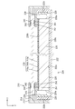
- FIG. 3 is a cross-sectional view of a cross section of the liquid crystal display device 10 cut along the vertical direction (Y-axis direction).
- the upper side shown in FIGS. 2 and 3 is the front side
- the lower side shown in FIGS. 2 and 3 is the back side.
- the liquid crystal display device 10 has a horizontally long rectangular shape as a whole, and includes a liquid crystal panel 16 as a display panel and a backlight device 24 as an external light source, and these form a bezel having a frame shape. 12 and the like are integrally held.
- a first buffer member 41 and a second buffer member 42 having a buffer function and holding the liquid crystal panel 16 are arranged between the bezel 12 and the liquid crystal panel 16. ing.
- the first buffer member 41 and the second buffer member 42 will be described in detail later.
- the liquid crystal panel 16 has a configuration in which a pair of transparent (highly translucent) glass substrates are bonded together with a predetermined gap therebetween, and a liquid crystal layer (not shown) is sealed between the glass substrates. Is done.
- One glass substrate is provided with a switching element (for example, TFT) connected to a source wiring and a gate wiring orthogonal to each other, a pixel electrode connected to the switching element, an alignment film, and the like.
- the substrate is provided with a color filter and counter electrodes in which colored portions such as R (red), G (green), and B (blue) are arranged in a predetermined arrangement, and an alignment film.
- image data and various control signals necessary for displaying an image are supplied to a source wiring, a gate wiring, a counter electrode, and the like from a drive circuit board (not shown).
- a polarizing plate (not shown) is disposed outside both glass substrates.
- the backlight device 24 includes a frame 14, an optical member 18, and a chassis 22.
- the frame 14 has a frame shape, is disposed along the edge side of the surface of the light guide plate 20 (light output surface 20b), and supports the liquid crystal panel 16 along the inner edge.
- the optical member 18 is placed on the front side of the light guide plate 20 (the light exit surface 20b side).
- the chassis 22 has a substantially box shape having a light emitting part 22d on the front side (light emitting side, liquid crystal panel 16 side).
- a pair of LED (Light Emitting Diode) units 32, 32, a reflection sheet 26, and a light guide plate 20 are accommodated.
- the pair of LED units 32 and 32 are respectively arranged on the long side outer edges (side plates) 22b and 22c of the chassis 22 and emit light.
- the longitudinal side surface (light incident surface) 20a of the light guide plate 20 is disposed at a position facing the LED units 32 and 32, and guides light emitted from the LED unit 32 to the liquid crystal panel 16 side.
- the optical member 18 is placed on the front side of the light guide plate 20.
- the light guide plate 20 and the optical member 18 are disposed directly below the liquid crystal panel 16 and the LED unit 32 that is a light source is disposed on the side end of the light guide plate 20.
- a so-called edge light system (side light system) is adopted.
- the chassis 22 is made of a metal such as an aluminum material, for example, and has a bottom plate 22a having a rectangular shape in a plan view, side plates 22b and 22c rising from outer edges of both long sides of the bottom plate 22a, and both short sides of the bottom plate 22a. It consists of a side plate that rises from the outer edge.
- a space facing the LED units 32, 32 in the chassis 22 is a housing space for the light guide plate 20.
- a power circuit board (not shown) for supplying power to the LED unit 32 is attached to the back side of the bottom plate 22a.
- the reflection sheet 26 is placed on the front side of the bottom plate 22 a of the chassis 22.
- the reflection sheet 26 has a reflection surface on the front side, and this reflection surface is opposed to the back surface (opposite surface 20 c) of the light guide plate 20, and reflects light leaked from the LED units 32, 32 to reflect light. It plays a role of entering the opposite surface 20 c of the light guide plate 20.
- the optical member 18 is formed by laminating a diffusion sheet 18a, a lens sheet 18b, and a reflective polarizing plate 18c in order from the light guide plate 20 side.
- the diffusion sheet 18a, the lens sheet 18b, and the reflective polarizing plate 18c have a function of converting light emitted from the LED unit 32 and passing through the light guide plate 20 into planar light.
- a liquid crystal panel 16 is installed on the upper surface side of the reflective polarizing plate 18 d, and the optical member 18 is disposed between the light guide plate 20 and the liquid crystal panel 16.
- the LED unit 32 has a configuration in which LED light sources 28 that emit white light are arranged in a row on a resin-made rectangular LED board 30.
- the surface opposite to the surface on which the LED light source 28 is disposed is disposed in contact with the heat radiating plate 36 of the chassis 22.
- the LED light source 28 may emit white light by applying a phosphor having a light emission peak in a yellow region to a blue light emitting element.
- the blue light emitting element may emit white light by applying a phosphor having emission peaks in the green and red regions.
- a phosphor having a light emission peak in a green region may be applied to a blue light emitting element, and white light may be emitted by combining a red light emitting element.
- the LED light source 28 may emit white light by combining a blue light emitting element, a green light emitting element, and a red light emitting element. Further, a combination of an ultraviolet light emitting element and a phosphor may be used. In particular, an ultraviolet light-emitting element may emit white light by applying a phosphor having emission peaks in blue, green, and red, respectively.
- the light guide plate 20 is a rectangular plate-like member, is formed of a resin having high translucency (high transparency) such as acrylic, and is placed on the reflection sheet 26 and supported by the chassis 22. ing. 2 and 3, the light guide plate 20 is a plate opposite to the light output surface 20b, with the light output surface 20b being the main plate surface facing the diffusion sheet 18a between the pair of LED units 32 and 32.
- the opposite surface 20c which is a surface, is arranged so as to face the reflection sheet 26 side.
- the light generated from the LED unit 32 enters the light entrance surface 20 a of the light guide plate 20 and exits from the light exit surface 20 b facing the diffusion sheet 18 a,
- the liquid crystal panel 16 is irradiated from the back side.
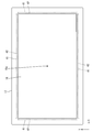
- FIG. 4 shows a plan view of the bezel 12 and the liquid crystal panel 16 as viewed from the front side.
- the first buffer member 41 and the second buffer member 42 have a buffer function, and are respectively disposed between the bezel 12 and the outer edge of the liquid crystal panel 16 as shown in FIG.
- the first buffer member 41 is made of urethane such as Polon (manufactured by Roger Sinoac).
- the second buffer member 42 is made of polyethylene terephthalate.
- the first buffer member 41 and the second buffer member 42 are each linear in a plan view, and four are arranged along each side of the bezel 12.
- the first buffer member 41 and the second buffer member 42 have a rectangular shape in cross-sectional view (see FIG. 3), and have the same shape.
- the second buffer member 42 is disposed closer to the center 16a of the liquid crystal panel 16 than the first buffer member 41, and is in contact with the first buffer member 41 adjacent to the first buffer member 41 in the plane direction (XY plane direction). ing.
- the first buffer member 41 is fixed to the back surface of the bezel 12 (the surface facing the outer edge of the liquid crystal panel 16) with an adhesive tape, for example, and is opposite to the surface attached to the bezel 12.
- the side surface is in contact with the outer edge end surface of the liquid crystal panel 16. For this reason, a frictional force acts between the first buffer member 41 and the liquid crystal panel 16, and the liquid crystal panel 16 is held by the first buffer member 41.
- the first buffer member 41 is pulled by the liquid crystal panel 16 due to this frictional force and is detached from the bezel 12, and the first buffer member 41 may be displaced. There is.
- the second buffer member 42 is not fixed to the bezel 12 or the liquid crystal panel 16, and is disposed so that both the front and back surfaces thereof are in contact with the bezel 12 and the liquid crystal panel 16, respectively.
- the polyethylene terephthalate constituting the second buffer member 42 has a smaller coefficient of friction than the urethane constituting the first buffer member 41. For this reason, even when the liquid crystal panel 16 moves in the plane direction, the second buffer member 42 and the liquid crystal panel 16 are easily slipped, and the second buffer member 42 is not easily dragged by the liquid crystal panel 16. Therefore, even when the liquid crystal panel 16 is moved such that the first buffer member 41 is displaced in the plane direction, the second buffer member 42 is held at that position.
- the liquid crystal display device 10 even if the first buffer member 41 is dragged and moved by the movement of the liquid crystal panel 16 due to vibration or the like, the second coefficient of friction is low. Since the buffer member 42 is difficult to be dragged by the display panel 16, its position is maintained. For this reason, when the 1st buffer member 41 moves and contacts the 2nd buffer member 42, it is prevented that the 1st buffer member 41 moves further, and position shift of the 1st buffer member 41 is carried out. Can be prevented or suppressed. As a result, it is possible to prevent or suppress deterioration of display characteristics in the liquid crystal display device 10.
- the first buffer member 41 and the second buffer member 42 are arranged adjacent to each other. For this reason, even if the first buffer member 41 is in contact with the second buffer member 42 from the beginning and the liquid crystal panel 16 is moved by vibration or the like, the first buffer member 41 is prevented from moving from the beginning. Therefore, the position shift of the 1st buffer member 41 can be prevented or suppressed effectively.
- the first buffer member 41 and the second buffer member 42 are arranged along each side of the bezel 12, respectively. For this reason, the liquid crystal panel 16 can be effectively held by the first buffer member 41, and the displacement of the first buffer member 41 can be effectively suppressed by the second buffer member 42. .
- the mounting mode of the first buffer member 41 is different from that of the first embodiment.
- both front and back surfaces of the first buffer member 41 are attached with an adhesive tape. That is, the surface of the first buffer member 41 is attached to the back surface of the bezel 12 with an adhesive tape, and further, the back surface of the first buffer member 41 is attached to the outer edge end surface of the liquid crystal panel 16 with the adhesive tape. Yes.
- the 1st buffer member 41 Since the 1st buffer member 41 is made into such an attachment mode, the 1st buffer member 41 is fixed more, so that the liquid crystal panel 16 can be effectively held by the 1st buffer member 41, The positional displacement of the first buffer member 41 can be further prevented or suppressed.
- FIG. 5 is a cross-sectional view of the liquid crystal display device 110 according to the second embodiment and shows a cross-sectional configuration corresponding to FIG. 3 of the first embodiment.
- FIG. 6 is a plan view of the bezel 112 and the liquid crystal panel 116 as viewed from the front side.
- the second embodiment is different from that of the first embodiment in that the second buffer members 142a and 142b are arranged on both sides of the first buffer member 141. Since the other configuration is the same as that of the first embodiment, description of the structure, operation, and effect is omitted. 5, the part where the numeral 100 is added to the reference numeral in FIG. 3 and the part where the numeral 100 is added to the reference numeral in FIG. 4 in FIG. 6 are the same as those described in the first embodiment.
- the second buffer members 142 a and 142 b are arranged on both sides of the first buffer member 141. That is, one second buffer member 142 a is arranged on the center side of the liquid crystal panel 116 with respect to the first buffer member 142, and the other second buffer member 142 b is disposed on the outer edge of the liquid crystal panel 116 with respect to the first buffer member 142.
- the second buffer members 142 a and 142 b are in contact with the first buffer member 141.
- the first buffer member 141 is formed in the plane direction by the second buffer member 142a disposed on the center side of the liquid crystal panel 116 and the second buffer member 142b disposed on the outer edge end side of the liquid crystal panel 116. It is in a clamped state. For this reason, in the liquid crystal display device 110, the second buffer members 142 a and 142 b not only cause the first buffer member 141 to be displaced toward the center of the liquid crystal panel 116, but also the outer edge end portion of the liquid crystal panel 116. Misalignment to the side can also be prevented or suppressed.
- each buffer member 141, 142a, 142b is arranged in a frame shape along the shape of the bezel 116, as shown in FIG. Therefore, the first buffer member 141 and the second buffer members 142a and 142b can have a buffering effect in all the regions along the shape of the bezel 116. Therefore, the liquid crystal panel 116 can be more effectively held by the first buffer member 141, and the displacement of the first buffer member 141 can be more effectively suppressed by the second buffer members 142a and 142b. .
- FIG. 7 is a cross-sectional view of the liquid crystal display device 210 according to the third embodiment, and shows a cross-sectional configuration corresponding to FIG. 3 of the first embodiment.
- the third embodiment is different from that of the first embodiment in that a buffer member is also disposed between the frame 214 and the liquid crystal panel 216. Since other configurations are the same as those of the first embodiment, description of the structure, operation, and effect is omitted.
- a part obtained by adding the numeral 200 to the reference numeral in FIG. 3 is the same as the part described in the first embodiment.
- the first buffer member 251 and the second buffer member 252 are also disposed between the frame 214 and the liquid crystal panel 216, respectively. .
- the first buffer member 251 and the second buffer member 252 are light guide plates 220 with respect to the first buffer member 241 and the second buffer member 242 disposed between the bezel 212 and the liquid crystal panel 216.
- the LED light sources 28, 128, and 228 are examples of “light sources”.
- the chassis 22, 122, and 222 are examples of “accommodating members”.
- the liquid crystal panels 16, 116, and 216 are examples of the “display panel”.
- the bezels 12, 112, and 212 are examples of the “first frame member”.
- the liquid crystal display devices 10, 110, and 210 are examples of the “display device”.
- the frames 14, 114, and 214 are examples of the “second frame member”.
- first buffer member and the second buffer member are adjacent to and in contact with each other.
- first buffer member and the second buffer member include The structure which is separated may be sufficient.
- first buffer member and the second buffer member are illustrated as being arranged along each side of the bezel or in a frame shape.
- the shape of the second buffer member is not limited. For example, a configuration in which block-shaped first buffer members and second buffer members are scattered along each side of the bezel may be employed.
- the first buffer member is made of urethane
- the second buffer member is made of polyethylene terephthalate.
- the material of the two buffer members is not limited.
- the shape, arrangement, material, and the like of the first buffer member and the second buffer member can be changed as appropriate.
- the television receiver provided with the tuner has been exemplified.
- the present invention can also be applied to a display device that does not include the tuner.
- TV TV receiver, Ca, Cb: cabinet, T: tuner, S: stand, 10, 110, 210: liquid crystal display, 12, 112, 212: bezel, 14, 114, 214: frame, 16, 116, 216: Liquid crystal panel, 18, 118, 218: Optical member, 20, 120, 220: Light guide plate, 20a, 120a, 220a: Light incident surface, 22, 122, 222: Chassis, 24, 124, 224: Backlight device , 26, 126, 226: reflection sheet, 28, 128, 228: LED light source, 30, 130, 230: LED substrate, 32, 132, 232: LED unit, 41, 141, 241, 251: first buffer member , 42, 142a, 142b, 242 and 252: second buffer members
Landscapes
- Physics & Mathematics (AREA)
- Nonlinear Science (AREA)
- Mathematical Physics (AREA)
- Chemical & Material Sciences (AREA)
- Crystallography & Structural Chemistry (AREA)
- General Physics & Mathematics (AREA)
- Optics & Photonics (AREA)
- Liquid Crystal (AREA)
Abstract
本発明に係る液晶表示装置10は、LED光源28と、底板22aと、底板22aの少なくとも一つの端辺から底板22aの表側に立ち上がる側板22bと、表側にLED光源28からの光を出光する出光部22dと、を有し、少なくともLED光源28を収容するシャーシ22と、シャーシ22の出光部22d側に配された液晶パネル16と、枠状をなし、液晶パネル16の外縁を覆うベゼル12と、液晶パネル16とベゼル12との間に両者に当接して配された第1の緩衝部材41と、第1の緩衝部材41より液晶パネル16の中心側において、液晶パネル16とベゼル12との間に両者に当接して配され、第1の緩衝部材41より摩擦係数が小さな第2の緩衝部材42とを備える。
Description
本発明は、表示装置、及びテレビ受信装置に関する。
近年、テレビ受信装置をはじめとする画像表示装置の表示素子は、従来のブラウン管から液晶パネルやプラズマディスプレイパネルなどの薄型表示素子を適用した薄型表示装置に移行しつつあり、画像表示装置の薄型化を可能としている。このような液晶表示装置では、液晶パネルを保護および保持するために枠状のベゼルやフレームが広く用いられている。
ベゼルは、液晶パネルの外縁に沿って嵌め込まれ、液晶パネルの外端部表面を覆うように配される。そして、ベゼルと液晶パネルの間には、ベゼルが液晶パネルと当接することによる液晶パネル表面の損傷等を防ぐため、ウレタン等の樹脂によって形成された緩衝部材が配されることがある。この緩衝部材によって、液晶パネル表面の損傷が防止されると共に、液晶パネルが保持される。また、フレームと液晶パネルの間においても、このような緩衝部材が配されることがある。
特許文献1に、ベゼルと液晶パネルの間に緩衝部材が配された液晶モジュールが開示されている。この液晶モジュールでは、ベゼルと液晶パネルの間に緩衝部材としての弾性体が配されている。弾性体は、ベゼルと対向する面が例えば両面テープ等の粘着テープによって固定されており、液晶パネルと対向する先端部が液晶パネルと当接している。これにより、ベゼルと液晶パネルとの間の隙間から埃等が侵入することが防止されている。
(発明が解決しようとする課題)
しかしながら、上記した特許文献1の液晶モジュールにおいて、液晶パネルが振動等によって平面方向(液晶パネルの板面方向)に移動すると、弾性体の先端部と液晶パネルとの間の摩擦によって弾性体が液晶パネルに引きずられ、弾性体がベゼルから外れてしまうことがある。その結果、弾性体が位置ずれして液晶パネルの表示面の一部を覆い、液晶モジュール(液晶表示装置)の表示特性が低下することがある。
しかしながら、上記した特許文献1の液晶モジュールにおいて、液晶パネルが振動等によって平面方向(液晶パネルの板面方向)に移動すると、弾性体の先端部と液晶パネルとの間の摩擦によって弾性体が液晶パネルに引きずられ、弾性体がベゼルから外れてしまうことがある。その結果、弾性体が位置ずれして液晶パネルの表示面の一部を覆い、液晶モジュール(液晶表示装置)の表示特性が低下することがある。
本明細書で開示される発明は、上記の課題に鑑みて創作されたものである。本明細書で開示される発明は、表示装置において表示特性が低下することを防止ないし抑制することができる技術を提供することを目的とする。
(課題を解決するための手段)
本明細書で開示される技術は、光源と、底板と、該底板の少なくとも一つの端辺から該底板の一方の面側に立ち上がる側板と、前記一方の面側に前記光源からの光を出光する出光部と、を有し、少なくとも前記光源を収容する収容部材と、前記収容部材の前記出光部側に配された表示パネルと、枠状をなし、前記表示パネルの外縁を覆う第1の枠状部材と、前記表示パネルと前記第1の枠状部材との間に両者に当接して配された第1の緩衝部材と、前記第1の緩衝部材より前記表示パネルの中心側において、前記表示パネルと前記第1の枠状部材との間に両者に当接して配され、前記第1の緩衝部材より摩擦係数が小さな第2の緩衝部材と、を備える表示装置に関する。
本明細書で開示される技術は、光源と、底板と、該底板の少なくとも一つの端辺から該底板の一方の面側に立ち上がる側板と、前記一方の面側に前記光源からの光を出光する出光部と、を有し、少なくとも前記光源を収容する収容部材と、前記収容部材の前記出光部側に配された表示パネルと、枠状をなし、前記表示パネルの外縁を覆う第1の枠状部材と、前記表示パネルと前記第1の枠状部材との間に両者に当接して配された第1の緩衝部材と、前記第1の緩衝部材より前記表示パネルの中心側において、前記表示パネルと前記第1の枠状部材との間に両者に当接して配され、前記第1の緩衝部材より摩擦係数が小さな第2の緩衝部材と、を備える表示装置に関する。
上記の表示装置によると、振動等による表示パネルの移動によって第1の緩衝部材が表示パネルに引きずられて移動したとしても、摩擦係数が低い第2の緩衝部材は表示パネルに引きずられ難いので、その位置が保持される。このため、第1の緩衝部材が移動して第2の緩衝部材と当接することで、第1の緩衝部材がそれ以上移動することが防止され、第1の緩衝部材の位置ずれを防止ないし抑制することができる。この結果、表示装置において表示特性が低下することを防止ないし抑制することができる。
前記第1の緩衝部材と前記第2の緩衝部材とが隣接して配されていてもよい。
この構成によると、第1の緩衝部材が当初から第2の緩衝部材と当接しているので、表示パネルが振動等によって移動したとしても、当初から第1の緩衝部材の移動が防止され、第1の緩衝部材の位置ずれを効果的に防止ないし抑制することができる。
この構成によると、第1の緩衝部材が当初から第2の緩衝部材と当接しているので、表示パネルが振動等によって移動したとしても、当初から第1の緩衝部材の移動が防止され、第1の緩衝部材の位置ずれを効果的に防止ないし抑制することができる。
前記第1の緩衝部材および前記第2の緩衝部材がそれぞれ前記第1の枠状部材の少なくとも1つの辺に沿って配されていてもよい。
この構成によると、第1の緩衝部材によって表示パネルを効果的に保持できると共に、第2の緩衝部材によって第1の緩衝部材の位置ずれを効果的に抑制することができる。
この構成によると、第1の緩衝部材によって表示パネルを効果的に保持できると共に、第2の緩衝部材によって第1の緩衝部材の位置ずれを効果的に抑制することができる。
前記第1の緩衝部材および前記第2の緩衝部材がそれぞれ枠状をなしてもよい。
この構成によると、第1の緩衝部材によって表示パネルを一層効果的に保持できると共に、第2の緩衝部材によって第1の緩衝部材の位置ずれを一層効果的に抑制することができる。
この構成によると、第1の緩衝部材によって表示パネルを一層効果的に保持できると共に、第2の緩衝部材によって第1の緩衝部材の位置ずれを一層効果的に抑制することができる。
複数の前記第2の緩衝部材を備え、前記第2の緩衝部材が前記第1の緩衝部材より前記表示パネルの外縁端部側にさらに配されていてもよい。
この構成によると、第1の緩衝部材が表示パネルの外縁端部側へ位置ずれすることを第2の緩衝部材によって防止ないし抑制することができる。
この構成によると、第1の緩衝部材が表示パネルの外縁端部側へ位置ずれすることを第2の緩衝部材によって防止ないし抑制することができる。
前記第1の緩衝部材が前記表示パネルにさらに固定されていてもよい。
この構成によると、第1の緩衝部材によって表示パネルを効果的に保持できると共に、第1の緩衝部材の位置ずれを一層防止ないし抑制することができる。
この構成によると、第1の緩衝部材によって表示パネルを効果的に保持できると共に、第1の緩衝部材の位置ずれを一層防止ないし抑制することができる。
前記側板の立ち上がり端部と前記表示パネルとの間に配された第2の枠状部材をさらに備え、前記第2の枠状部材と前記表示パネルとの間に前記第1の緩衝部材と前記第2の緩衝部材とが配されていてもよい。
この構成によると、第2の枠状部材と表示パネルとの間に配された第1の緩衝部材と第2の緩衝部材とによって、表示パネルを一層保持できると共に、第2の緩衝部材の位置ずれを一層防止ないし抑制することができる。
この構成によると、第2の枠状部材と表示パネルとの間に配された第1の緩衝部材と第2の緩衝部材とによって、表示パネルを一層保持できると共に、第2の緩衝部材の位置ずれを一層防止ないし抑制することができる。
前記第1の緩衝部材はウレタンよりなってもよい。
この構成によると、第1の緩衝部材の具体的な構成を実現することができる。
この構成によると、第1の緩衝部材の具体的な構成を実現することができる。
前記第2の緩衝部材はポリエチレンテレフタラートよりなってもよい。
この構成によると、第2の緩衝部材の具体的な構成を実現することができる。
この構成によると、第2の緩衝部材の具体的な構成を実現することができる。
本明細書で開示される技術では、上記の表示パネルを、液晶を用いた液晶パネルとする表示装置も、新規で有用である。また、上記の表示装置を備えるテレビ受信装置も、新規で有用である。
(発明の効果)
本明細書で開示される技術によれば、表示装置において表示特性が低下することを防止ないし抑制することができる技術を提供することができる。
本明細書で開示される技術によれば、表示装置において表示特性が低下することを防止ないし抑制することができる技術を提供することができる。
<実施形態1>
図面を参照して実施形態1を説明する。なお、各図面の一部にはX軸、Y軸およびZ軸を示しており、各軸方向が各図面で共通した方向となるように描かれている。このうちY軸方向は、鉛直方向と一致し、X軸方向は、水平方向と一致している。また、特に断りがない限りは、上下の記載については鉛直方向を基準とする。
図面を参照して実施形態1を説明する。なお、各図面の一部にはX軸、Y軸およびZ軸を示しており、各軸方向が各図面で共通した方向となるように描かれている。このうちY軸方向は、鉛直方向と一致し、X軸方向は、水平方向と一致している。また、特に断りがない限りは、上下の記載については鉛直方向を基準とする。
図1は、実施形態1に係るテレビ受信装置TVの分解斜視図を示している。テレビ受信装置TVは、液晶表示装置10と、当該液晶表示装置10を挟むようにして収容する表裏両キャビネットCa、Cbと、電源Pと、チューナーTと、スタンドSと、を備えている。
図2は、液晶表示装置10の分解斜視図を示している。また、図3は、液晶表示装置10を鉛直方向(Y軸方向)に沿って切断した断面の断面図を示している。ここで、図2及び図3に示す上側を表側とし、図2及び図3に示す下側を裏側とする。図2に示すように、液晶表示装置10は、全体として横長の方形を成し、表示パネルである液晶パネル16と、外部光源であるバックライト装置24とを備え、これらが枠状を成すベゼル12などにより一体的に保持されるようになっている。また、図3に示すように、ベゼル12と液晶パネル16の間には、緩衝機能を有し、液晶パネル16を保持するための第1の緩衝部材41と第2の緩衝部材42が配されている。第1の緩衝部材41と第2の緩衝部材42については、後で詳しく説明する。
続いて、液晶パネル16について説明する。液晶パネル16は、透明な(高い透光性を有する)一対のガラス基板が所定のギャップを隔てた状態で貼り合わせられるとともに、両ガラス基板間に液晶層(図示しない)が封入された構成とされる。一方のガラス基板には、互いに直交するソース配線とゲート配線とに接続されたスイッチング素子(例えばTFT)と、そのスイッチング素子に接続された画素電極、さらには配向膜等が設けられ、他方のガラス基板には、R(赤色),G(緑色),B(青色)等の各着色部が所定配列で配置されたカラーフィルタや対向電極、さらには配向膜等が設けられている。このうち、ソース配線、ゲート配線および対向電極などには、図示しない駆動回路基板から画像を表示するのに必要な画像データや各種制御信号が供給されるようになっている。なお、両ガラス基板の外側には偏光板(図示しない)が配されている。
続いて、バックライト装置24について説明する。図2及び図3に示すように、バックライト装置24は、フレーム14と、光学部材18と、シャーシ22とを備えている。フレーム14は、枠状を成しており、導光板20の表面(出光面20b)の端縁側に沿って配され、内縁に沿って液晶パネル16を支持している。光学部材18は、導光板20の表側(出光面20b側)に載置されている。シャーシ22は、表側(光出射側、液晶パネル16側)に出光部22dを有した略箱型を成している。
シャーシ22内には、一対のLED(Light Emitting Diode)ユニット32,32と、反射シート26と、導光板20とが収容されている。一対のLEDユニット32,32は、それぞれシャーシ22の各長辺側外縁(側板)22b、22cに配されており、光を出射する。導光板20の長手方向側面(入光面)20aは各LEDユニット32,32と対向する位置に配されており、当該LEDユニット32から出射される光を液晶パネル16側へ導く。そして、この導光板20の表側に光学部材18が載置されている。本実施形態に係るバックライト装置24では、導光板20および光学部材18が液晶パネル16の直下に配されていると共に光源であるLEDユニット32が導光板20の側端部に配されてなる、いわゆるエッジライト方式(サイドライト方式)を採用している。
シャーシ22は、例えばアルミ系材料などの金属製とされ、平面視矩形状を成す底板22aと、底板22aの両長辺の各外縁から立ち上がる側板22b、22cと、底板22aの両短辺の各外縁から立ち上がる側板とから構成されている。シャーシ22内において各LEDユニット32,32と対向する空間が、導光板20用の収容空間となっている。なお、底板22aの裏側には、LEDユニット32に電力を供給する電源回路基板(図示しない)等が取り付けられている。
反射シート26は、シャーシ22の底板22aの表側に載置されている。反射シート26は、その表側に反射面を有し、この反射面が導光板20の裏面(反対面20c)と対向しており、LEDユニット32,32から漏れた光を反射させることで光を導光板20の反対面20cに入射させる役割を果たしている。
光学部材18は、導光板20側から順に、拡散シート18a、レンズシート18b、反射型偏光板18cが積層されたものである。拡散シート18a、レンズシート18b、反射型偏光板18cは、LEDユニット32から出射され、導光板20を通過した光を面状の光とする機能を有している。反射型偏光板18dの上面側には液晶パネル16が設置されており、光学部材18は導光板20と液晶パネル16との間に配されている。
LEDユニット32は、樹脂製の矩形状を成すLED基板30に、白色発光するLED光源28が一列に並んだ構成となっている。LED光源28が配された面とは反対側の面がシャーシ22の放熱板36と当接した状態で配されている。なお、LED光源28は、青色発光素子に、黄色の領域に発光ピークを持つ蛍光体を塗布することにより白色発光するものとしたものであってもよい。また、青色発光素子に、緑色と赤色の領域にそれぞれ発光ピークを持つ蛍光体を塗布することにより白色発光するものとしたものであってもよい。また、青色発光素子に、緑色の領域に発光ピークを持つ蛍光体を塗布すると共に、赤色発光素子を組み合わせることにより白色発光するものとしたものであってもよい。また、LED光源28は、青色発光素子と、緑色発光素子と、赤色発光素子と、を組み合わせることにより白色発光するものとしたものであってもよい。また、紫外光発光素子と、蛍光体と、を組み合わせたものであってもよい。特に、紫外光発光素子に、青色と緑色と赤色にそれぞれ発光ピークを持つ蛍光体を塗布することにより白色発光するものとしたものであってもよい。
導光板20は、矩形状の板状部材とされ、アクリル等の透光性の大きい(透明度の高い)樹脂により形成されており、反射シート26上に載置されると共に、シャーシ22によって支持されている。導光板20は、図2及び図3に示すように、一対のLEDユニット32,32の間に、主板面である出光面20bを拡散シート18a側に向け、出光面20bとは反対側の板面である反対面20cを反射シート26側に向ける形で配されている。このような導光板20が配設されることにより、LEDユニット32から生じた光は、導光板20の入光面20aから入射して拡散シート18aと対向する出光面20bから出射することで、液晶パネル16をその背面側から照射する。
続いて本実施形態の要部である第1の緩衝部材41及び第2の緩衝部材42の構成について説明する。ここで、図4に、ベゼル12と液晶パネル16を表側から視た平面図を示す。第1の緩衝部材41及び第2の緩衝部材42は、緩衝機能を有し、図3に示すように、それぞれベゼル12と液晶パネル16の外縁端部との間に配されている。第1の緩衝部材41は、例えばポロン(ロジャースイノアック社製)のようなウレタンによりなっている。また、第2の緩衝部材42は、ポリエチレンテレフタラートによりなっている。
第1の緩衝部材41及び第2の緩衝部材42は、図4に示すように、平面視においてそれぞれ線状をなし、ベゼル12の各辺に沿ってそれぞれ4つ配されている。また、第1の緩衝部材41及び第2の緩衝部材42は、断面視においてそれぞれ矩形状をなしており(図3参照)、互いに同形状となっている。また、第2の緩衝部材42は、第1の緩衝部材41より液晶パネル16の中心16a側に配され、平面方向(X-Y平面方向)において第1の緩衝部材41と隣接して当接している。
第1の緩衝部材41は、例えば粘着テープによってベゼル12の裏面(液晶パネル16の外縁端部と対向する面)に貼り付けられて固定されており、ベゼル12に貼り付けられた面とは反対側の面が液晶パネル16の外縁端部表面と当接している。このため、第1の緩衝部材41と液晶パネル16との間には摩擦力が働き、液晶パネル16が第1の緩衝部材41によって保持される。一方で、液晶パネル16が振動等により平面方向に移動すると、この摩擦力によって第1の緩衝部材41が液晶パネル16に引きずられてベゼル12から外れ、第1の緩衝部材41が位置ずれする虞がある。
第2の緩衝部材42は、ベゼル12又は液晶パネル16には固定されておらず、その表裏両面がそれぞれベゼル12と液晶パネル16とに当接するように配されている。ここで、第2の緩衝部材42を構成するポリエチレンテレフタラートは、第1の緩衝部材41を構成するウレタンより摩擦係数が小さい。このため、液晶パネル16が平面方向に移動した場合であっても、第2の緩衝部材42と液晶パネル16の間は滑り易く、第2の緩衝部材42は液晶パネル16に引きずられ難い。従って、第1の緩衝部材41が平面方向に位置ずれするような液晶パネル16の移動が生じた場合であっても、第2の緩衝部材42はその位置が保持されることとなる。
以上のように本実施形態に係る液晶表示装置10では、振動等による液晶パネル16の移動によって第1の緩衝部材41が液晶パネル16に引きずられて移動したとしても、摩擦係数が低い第2の緩衝部材42は表示パネル16に引きずられ難いので、その位置が保持される。このため、第1の緩衝部材41が移動して第2の緩衝部材42と当接することで、第1の緩衝部材41がそれ以上移動することが防止され、第1の緩衝部材41の位置ずれを防止ないし抑制することができる。この結果、液晶表示装置10における表示特性が低下することを防止ないし抑制することができる。
また、本実施形態に係る液晶表示装置10では、第1の緩衝部材41と第2の緩衝部材42とが隣接して配されている。このため、第1の緩衝部材41が当初から第2の緩衝部材42と当接しており、液晶パネル16が振動等によって移動したとしても、当初から第1の緩衝部材41の移動が防止されるので、第1の緩衝部材41の位置ずれを効果的に防止ないし抑制することができる。
また、本実施形態に係る液晶表示装置10では、第1の緩衝部材41および第2の緩衝部材42がそれぞれベゼル12の各辺に沿って配されている。このため、第1の緩衝部材41によって液晶パネル16を効果的に保持することができ、さらに、第2の緩衝部材42によって第1の緩衝部材41の位置ずれを効果的に抑制することができる。
<実施形態1の変形例>
続いて実施形態1の変形例を説明する。変形例は、第1の緩衝部材41の取付態様が実施形態1のものと異なっている。変形例では、第1の緩衝部材41の表裏両面が粘着テープで貼りつけられている。即ち、第1の緩衝部材41の表面が粘着テープによってベゼル12の裏面に貼り付けられ、さらに、第1の緩衝部材41の裏面が粘着テープによって液晶パネル16の外縁端部表面に貼り付けられている。第1の緩衝部材41がこのような取付態様とされていることにより、第1の緩衝部材41がより固定されるので、第1の緩衝部材41によって液晶パネル16を効果的に保持できると共に、第1の緩衝部材41の位置ずれを一層防止ないし抑制することができる。
続いて実施形態1の変形例を説明する。変形例は、第1の緩衝部材41の取付態様が実施形態1のものと異なっている。変形例では、第1の緩衝部材41の表裏両面が粘着テープで貼りつけられている。即ち、第1の緩衝部材41の表面が粘着テープによってベゼル12の裏面に貼り付けられ、さらに、第1の緩衝部材41の裏面が粘着テープによって液晶パネル16の外縁端部表面に貼り付けられている。第1の緩衝部材41がこのような取付態様とされていることにより、第1の緩衝部材41がより固定されるので、第1の緩衝部材41によって液晶パネル16を効果的に保持できると共に、第1の緩衝部材41の位置ずれを一層防止ないし抑制することができる。
<実施形態2>
図面を参照して実施形態2を説明する。図5は、実施形態2に係る液晶表示装置110の断面図であって、実施形態1の図3と対応する断面の断面構成を示している。図6は、ベゼル112と液晶パネル116を表側から視た平面図を示している。実施形態2は、第2の緩衝部材142a,142bが第1の緩衝部材141の両側に配されている点で実施形態1のものと異なっている。その他の構成については実施形態1と同じであるため、構造、作用、及び効果の説明は省略する。なお、図5において図3の参照符号に数字100を加えた部位及び図6において図4の参照符号に数字100を加えた部位は、実施形態1で説明した部位と同一である。
図面を参照して実施形態2を説明する。図5は、実施形態2に係る液晶表示装置110の断面図であって、実施形態1の図3と対応する断面の断面構成を示している。図6は、ベゼル112と液晶パネル116を表側から視た平面図を示している。実施形態2は、第2の緩衝部材142a,142bが第1の緩衝部材141の両側に配されている点で実施形態1のものと異なっている。その他の構成については実施形態1と同じであるため、構造、作用、及び効果の説明は省略する。なお、図5において図3の参照符号に数字100を加えた部位及び図6において図4の参照符号に数字100を加えた部位は、実施形態1で説明した部位と同一である。
実施形態2に係る液晶表示装置110では、図5に示すように、第2の緩衝部材142a,142bが第1の緩衝部材141の両側に配されている。即ち、一方の第2の緩衝部材142aが第1の緩衝部材142より液晶パネル116の中央側に配され、他方の第2の緩衝部材142bが第1の緩衝部材142より液晶パネル116の外縁端部側に配され、各第2の緩衝部材142a,142bは第1の緩衝部材141と当接している。従って、第1の緩衝部材141は、液晶パネル116の中央側に配された第2の緩衝部材142aと液晶パネル116の外縁端部側に配された第2の緩衝部材142bとによって平面方向に挟持された状態となっている。このため、液晶表示装置110では、第2の緩衝部材142a,142bによって、第1の緩衝部材141が、液晶パネル116の中央部側へ位置ずれすることだけでなく、液晶パネル116の外縁端部側へ位置ずれすることも防止ないし抑制することができる。
また、各緩衝部材141、142a、142bは、図6に示すように、ベゼル116の形状に沿ってそれぞれ枠状に配されている。このため、第1の緩衝部材141及び第2の緩衝部材142a、142bでは、ベゼル116の形状に沿った全ての領域において、緩衝効果を持たせることができる。このため、第1の緩衝部材141によって液晶パネル116を一層効果的に保持できると共に、第2の緩衝部材142a、142bによって第1の緩衝部材141の位置ずれを一層効果的に抑制することができる。
<実施形態3>
図面を参照して実施形態3を説明する。図7は、実施形態3に係る液晶表示装置210の断面図であって、実施形態1の図3と対応する断面の断面構成を示している。実施形態3は、フレーム214と液晶パネル216との間においても緩衝部材が配されている点で実施形態1のものと異なっている。その他の構成については実施形態1のものと同様であるため、構造、作用、及び効果の説明は省略する。なお、図7において、図3の参照符号に数字200を加えた部位は、実施形態1で説明した部位と同一である。
図面を参照して実施形態3を説明する。図7は、実施形態3に係る液晶表示装置210の断面図であって、実施形態1の図3と対応する断面の断面構成を示している。実施形態3は、フレーム214と液晶パネル216との間においても緩衝部材が配されている点で実施形態1のものと異なっている。その他の構成については実施形態1のものと同様であるため、構造、作用、及び効果の説明は省略する。なお、図7において、図3の参照符号に数字200を加えた部位は、実施形態1で説明した部位と同一である。
実施形態3に係る液晶表示装置210では、図7に示すように、フレーム214と液晶パネル216との間においても、第1の緩衝部材251と第2の緩衝部材252とがそれぞれ配されている。これらの第1の緩衝部材251と第2の緩衝部材252は、ベゼル212と液晶パネル216との間に配された第1の緩衝部材241と第2の緩衝部材242とに対して導光板220の厚み方向(Z軸方向)にそれぞれ重畳するような配置で設けられている。このような構成とされていることにより、液晶表示装置210では、フレーム214と液晶パネル216との間に配された第1の緩衝部材251と第2の緩衝部材252とによって、液晶パネル216を一層保持できると共に、第2の緩衝部材242の位置ずれを一層防止ないし抑制することができる。
各実施形態の構成と本発明の構成との対応関係を記載しておく。LED光源28、128、228が「光源」の一例である。また、シャーシ22、122、222が「収容部材」の一例である。また、液晶パネル16、116、216が「表示パネル」の一例である。また、ベゼル12、112、212が「第1の枠状部材」の一例である。また、液晶表示装置10、110、210が「表示装置」の一例である。また、フレーム14、114、214が「第2の枠状部材」の一例である。
上記の各実施形態の変形例を以下に列挙する。
(1)上記の各実施形態では、第1の緩衝部材と第2の緩衝部材とが隣接して互いに当接している構成を例示したが、第1の緩衝部材と第2の緩衝部材とが離間している構成であってもよい。
(1)上記の各実施形態では、第1の緩衝部材と第2の緩衝部材とが隣接して互いに当接している構成を例示したが、第1の緩衝部材と第2の緩衝部材とが離間している構成であってもよい。
(2)上記の各実施形態では、第1の緩衝部材と第2の緩衝部材とがベゼルの各辺に沿って、又は枠状に配された構成を例示したが、第1の緩衝部材と第2の緩衝部材の形状は限定されない。例えば、ブロック状をなす第1の緩衝部材と第2の緩衝部材とがベゼルの各辺に沿って点在して配されている構成であってもよい。
(3)上記の各実施形態では、第1の緩衝部材がウレタンによりなっており、第2の緩衝部材がポリエチレンテレフタラートによりなっている構成を例示したが、第1の緩衝部材の材料及び第2の緩衝部材の材料は限定されない。
(4)上記の各実施形態以外にも第1の緩衝部材及び第2の緩衝部材の形状、配置、材料等は適宜に変更可能である。
(5)上記の各実施形態では、表示パネルとして液晶パネルを用いた液晶表示装置を例示したが、他の種類の表示パネルを用いた表示装置にも本発明は適用可能である。
(5)上記の各実施形態では、チューナーを備えたテレビ受信装置を例示したが、チューナーを備えない表示装置にも本発明は適用可能である。
以上、本発明の各実施形態について詳細に説明したが、これらは例示に過ぎず、特許請求の範囲を限定するものではない。特許請求の範囲に記載の技術には、以上に例示した具体例を様々に変形、変更したものが含まれる。
また、本明細書または図面に説明した技術要素は、単独であるいは各種の組合せによって技術的有用性を発揮するものであり、出願時の請求項に記載の組合せに限定されるものではない。また、本明細書または図面に例示した技術は複数目的を同時に達成し得るものであり、そのうちの一つの目的を達成すること自体で技術的有用性を持つものである。
TV:テレビ受信装置、Ca、Cb:キャビネット、T:チューナー、S:スタンド、10、110、210:液晶表示装置、12、112、212:ベゼル、14、114、214:フレーム、16、116、216:液晶パネル、18、118、218:光学部材、20、120、220:導光板、20a、120a、220a:入光面、22、122、222:シャーシ、24、124、224:バックライト装置、26、126、226:反射シート、28、128、228:LED光源、30、130、230:LED基板、32、132、232:LEDユニット、41、141、241、251:第1の緩衝部材、42、142a、142b、242、252:第2の緩衝部材
Claims (11)
- 光源と、
底板と、該底板の少なくとも一つの端辺から該底板の一方の面側に立ち上がる側板と、前記一方の面側に前記光源からの光を出光する出光部と、を有し、少なくとも前記光源を収容する収容部材と、
前記収容部材の前記出光部側に配された表示パネルと、
枠状をなし、前記表示パネルの外縁を覆う第1の枠状部材と、
前記表示パネルと前記第1の枠状部材との間に両者に当接して配された第1の緩衝部材と、
前記第1の緩衝部材より前記表示パネルの中心側において、前記表示パネルと前記第1の枠状部材との間に両者に当接して配され、前記第1の緩衝部材より摩擦係数が小さな第2の緩衝部材と、
を備えることを特徴とする表示装置。 - 前記第1の緩衝部材と前記第2の緩衝部材とが隣接して配されていることを特徴とする請求項1に記載の表示装置。
- 前記第1の緩衝部材および前記第2の緩衝部材がそれぞれ前記第1の枠状部材の少なくとも1つの辺に沿って配されていることを特徴とする請求項1又は請求項2に記載の表示装置。
- 前記第1の緩衝部材および前記第2の緩衝部材がそれぞれ枠状をなすことを特徴とする請求項3に記載の表示装置。
- 複数の前記第2の緩衝部材を備え、
少なくとも1つの前記第2の緩衝部材が前記第1の緩衝部材より前記表示パネルの外縁端部側にさらに配されていることを特徴とする請求項1から請求項4のいずれか1項に記載の表示装置。 - 前記第1の緩衝部材が前記表示パネルにさらに固定されていることを特徴とする請求項1から請求項5のいずれか1項に記載の表示装置。
- 前記側板の立ち上がり端部と前記表示パネルとの間に配された第2の枠状部材をさらに備え、
前記第2の枠状部材と前記表示パネルとの間に前記第1の緩衝部材と前記第2の緩衝部材とが配されていることを特徴とする請求項1から請求項6のいずれか1項に記載の表示装置。 - 前記第1の緩衝部材はウレタンよりなることを特徴とする請求項1から請求項7のいずれか1項に記載の表示装置。
- 前記第2の緩衝部材はポリエチレンテレフタラートよりなることを特徴とする請求項1から請求項8のいずれか1項に記載の表示装置。
- 前記表示パネルが液晶を用いた液晶パネルであることを特徴とする請求項1から請求項9のいずれか1項に記載の表示装置。
- 請求項1から請求項10のいずれか1項に記載の表示装置を備えることを特徴とするテレビ受信装置。
Applications Claiming Priority (2)
| Application Number | Priority Date | Filing Date | Title |
|---|---|---|---|
| JP2011-134153 | 2011-06-16 | ||
| JP2011134153 | 2011-06-16 |
Publications (1)
| Publication Number | Publication Date |
|---|---|
| WO2012173077A1 true WO2012173077A1 (ja) | 2012-12-20 |
Family
ID=47357064
Family Applications (1)
| Application Number | Title | Priority Date | Filing Date |
|---|---|---|---|
| PCT/JP2012/064882 Ceased WO2012173077A1 (ja) | 2011-06-16 | 2012-06-11 | 表示装置、及びテレビ受信装置 |
Country Status (1)
| Country | Link |
|---|---|
| WO (1) | WO2012173077A1 (ja) |
Cited By (3)
| Publication number | Priority date | Publication date | Assignee | Title |
|---|---|---|---|---|
| CN102981186A (zh) * | 2012-12-22 | 2013-03-20 | 张森 | 一种便携式车辆底盘图像信息采集装置 |
| CN103676278A (zh) * | 2013-12-16 | 2014-03-26 | 京东方科技集团股份有限公司 | 一种框架、背光模组和显示装置 |
| JP2019148722A (ja) * | 2018-02-27 | 2019-09-05 | シャープ株式会社 | 表示装置、テレビジョン受信機及び表示装置の製造方法 |
Citations (3)
| Publication number | Priority date | Publication date | Assignee | Title |
|---|---|---|---|---|
| JP2008096851A (ja) * | 2006-10-14 | 2008-04-24 | Sharp Corp | 表示装置 |
| JP2010060658A (ja) * | 2008-09-01 | 2010-03-18 | Sharp Corp | 画像表示装置 |
| JP2010073506A (ja) * | 2008-09-19 | 2010-04-02 | Hitachi Ltd | 液晶表示装置及びこれを用いた映像表示装置 |
-
2012
- 2012-06-11 WO PCT/JP2012/064882 patent/WO2012173077A1/ja not_active Ceased
Patent Citations (3)
| Publication number | Priority date | Publication date | Assignee | Title |
|---|---|---|---|---|
| JP2008096851A (ja) * | 2006-10-14 | 2008-04-24 | Sharp Corp | 表示装置 |
| JP2010060658A (ja) * | 2008-09-01 | 2010-03-18 | Sharp Corp | 画像表示装置 |
| JP2010073506A (ja) * | 2008-09-19 | 2010-04-02 | Hitachi Ltd | 液晶表示装置及びこれを用いた映像表示装置 |
Cited By (6)
| Publication number | Priority date | Publication date | Assignee | Title |
|---|---|---|---|---|
| CN102981186A (zh) * | 2012-12-22 | 2013-03-20 | 张森 | 一种便携式车辆底盘图像信息采集装置 |
| CN102981186B (zh) * | 2012-12-22 | 2016-04-20 | 张森 | 一种便携式车辆底盘图像信息采集装置 |
| CN103676278A (zh) * | 2013-12-16 | 2014-03-26 | 京东方科技集团股份有限公司 | 一种框架、背光模组和显示装置 |
| CN103676278B (zh) * | 2013-12-16 | 2016-09-21 | 京东方科技集团股份有限公司 | 一种框架、背光模组和显示装置 |
| JP2019148722A (ja) * | 2018-02-27 | 2019-09-05 | シャープ株式会社 | 表示装置、テレビジョン受信機及び表示装置の製造方法 |
| JP7084741B2 (ja) | 2018-02-27 | 2022-06-15 | シャープ株式会社 | 表示装置、テレビジョン受信機及び表示装置の製造方法 |
Similar Documents
| Publication | Publication Date | Title |
|---|---|---|
| US9322980B2 (en) | Illumination device, display device, and television receiving device | |
| US9632233B2 (en) | Display device and television device | |
| US20140204275A1 (en) | Illumination device, display device, and television reception device | |
| US20120281151A1 (en) | Lighting device, display device and television receiver | |
| US9116275B2 (en) | Illumination device, display device, and television receiving device | |
| US8998476B2 (en) | Lighting device, display device, and television receiving device | |
| US20150362652A1 (en) | Lighting device, display device, and television receiving device | |
| US9507080B2 (en) | Lighting device, display device and television device | |
| US20120268656A1 (en) | Lighting device, display device and television receiver | |
| JP6616448B2 (ja) | 表示装置 | |
| US20150124177A1 (en) | Lighting device, display device and television device | |
| WO2011074354A1 (ja) | 照明装置、表示装置およびテレビ受信装置 | |
| US20120262634A1 (en) | Lighting device, display device and television receiver | |
| WO2011086814A1 (ja) | 照明装置、表示装置およびテレビ受信装置 | |
| US20120287352A1 (en) | Lighting device, display device and television receiver | |
| US9234996B2 (en) | Display device and television device having holding member | |
| WO2012173077A1 (ja) | 表示装置、及びテレビ受信装置 | |
| US20140132848A1 (en) | Illuminating device, display device, and television receiver | |
| WO2011158553A1 (ja) | 照明装置、表示装置及びテレビ受信装置 | |
| WO2013031672A1 (ja) | 照明装置、表示装置、及びテレビ受信装置 | |
| WO2012111501A1 (ja) | 照明装置、表示装置、及びテレビ受信装置 | |
| JP2013206574A (ja) | 照明装置、表示装置、及びテレビ受信装置 | |
| WO2013038977A1 (ja) | 照明装置、表示装置、及びテレビ受信装置 | |
| WO2013051472A1 (ja) | 表示装置、及びテレビ受信装置 | |
| US20150103259A1 (en) | Lighting device, display device and television device |
Legal Events
| Date | Code | Title | Description |
|---|---|---|---|
| 121 | Ep: the epo has been informed by wipo that ep was designated in this application |
Ref document number: 12800959 Country of ref document: EP Kind code of ref document: A1 |
|
| NENP | Non-entry into the national phase |
Ref country code: DE |
|
| 122 | Ep: pct application non-entry in european phase |
Ref document number: 12800959 Country of ref document: EP Kind code of ref document: A1 |
|
| NENP | Non-entry into the national phase |
Ref country code: JP |