WO2012172708A1 - バックアップ装置およびバックアップ装置の動作方法 - Google Patents
バックアップ装置およびバックアップ装置の動作方法 Download PDFInfo
- Publication number
- WO2012172708A1 WO2012172708A1 PCT/JP2011/078511 JP2011078511W WO2012172708A1 WO 2012172708 A1 WO2012172708 A1 WO 2012172708A1 JP 2011078511 W JP2011078511 W JP 2011078511W WO 2012172708 A1 WO2012172708 A1 WO 2012172708A1
- Authority
- WO
- WIPO (PCT)
- Prior art keywords
- memory
- work memory
- log data
- storage
- backup device
- Prior art date
- Legal status (The legal status is an assumption and is not a legal conclusion. Google has not performed a legal analysis and makes no representation as to the accuracy of the status listed.)
- Ceased
Links
Images



Classifications
-
- G—PHYSICS
- G06—COMPUTING OR CALCULATING; COUNTING
- G06F—ELECTRIC DIGITAL DATA PROCESSING
- G06F11/00—Error detection; Error correction; Monitoring
- G06F11/07—Responding to the occurrence of a fault, e.g. fault tolerance
- G06F11/14—Error detection or correction of the data by redundancy in operations
- G06F11/1446—Point-in-time backing up or restoration of persistent data
- G06F11/1456—Hardware arrangements for backup
Definitions
- the present invention relates to a backup device that backs up log data created by a computer and an operation method of the backup device.
- an uninterruptible power supply is sometimes attached to a computer in order to operate the computer safely (JP 2009-3789, FIG. 2 (Patent Document 1)).
- the computer is supplied with power from a commercial power source, and the UPS is supplied with power for charging from the commercial power source.
- power loss When a power failure occurs in a commercial power supply (hereinafter referred to as “power loss”), log data created by a computer can be safely and reliably stored by supplying electricity from a battery built into the UPS as a power source for the computer. Can be saved.
- the UPS when the UPS is provided, the log data can be stored safely and reliably.
- the UPS since the UPS is generally large, it is difficult to secure an installation space and the cost of the UPS is high.
- the log data to be backed up created by the computer has a small capacity (for example, 4 MB or less), the log data can be saved at a small size and at a low cost by using, for example, a battery-backed SRAM.
- a battery-backed SRAM has a relatively small storage capacity. For this reason, in the method using only the SRAM, when the log data to be backed up has a large capacity (several tens of MB), the number of SRAM (the number of parts) increases to increase the size and cost.
- an object of the present invention is to provide a backup device that can store a large amount of log data safely and reliably, and can be realized in a small size and at a low cost.
- the backup device of the present invention provides: Work memory consisting of SRAM that can be battery-backed stored data, A storage memory composed of a non-volatile memory having a higher recording density than the work memory; An interface unit interposed between the host computer and the work memory and the storage memory, and allowing the host computer to access the work memory and the storage memory; And a control unit that performs control to transfer and store the log data transferred from the host computer to the work memory via the interface unit and stored in the storage memory.
- the backup device of the present invention stores a large amount of log data as follows.
- the host computer transfers a part of a large amount of log data to the work memory via the interface unit.
- the control unit controls the work memory, and transfers and stores the part of the log data to the storage memory.
- the control unit transfers and stores another part of the log data to the storage memory.
- the control unit sequentially transfers a part of the log data to the storage memory and stores it. Since the work memory is composed of SRAM, the log data can be stored in the work memory at a relatively high speed. On the other hand, since the storage memory has a higher recording density than the work memory, a larger amount of log data can be stored in the storage memory.
- the work memory is composed of SRAM which can be backed up by a battery
- the storage memory is composed of nonvolatile memory. Therefore, even if the power is cut off, the log data can be kept in the work memory or the storage memory. For this reason, a large amount of the log data can be stored safely and reliably.
- this backup device can be realized with a relatively small size and low cost by using commercially available parts, and space and UPS costs can be omitted as compared with the case where a UPS is provided.
- the storage memory is omitted and the log data is backed up only with the work memory made of SRAM, the number of SRAMs (number of parts) increases, resulting in an increase in size and cost.
- the storage memory composed of the nonvolatile memory has a relatively slow operation speed, so the log data is stored in the storage memory. The speed is slow.
- a power-off detector that detects that a power-off has occurred; When the power-off detection unit detects the power-off, a cutoff control unit that performs control to cut off access to the work memory and the storage memory; When returning from the power-off, a part of the log data stored in the work memory is transferred to the storage memory when the power-off occurs, and another part of the log data remains.
- a transfer state detection unit that detects whether or not it was in the middle, When the transfer state detection unit detects that the transfer state is in the middle of the transfer when the power interruption occurs, the control unit detects the other log data that remains untransferred in the work memory. Control is performed to transfer the portion to the storage memory and store it.
- the power interruption detection unit detects the power interruption. Then, the blocking control unit performs control to block access to the storage memory.
- the power interruption occurs, if the log data stored in the work memory is in the process of being transferred to the storage memory, the part of the log data is transferred to the storage memory, and The other part of the log data remains untransferred in the work memory (this is referred to as a “transfer-in-progress state”).
- the transfer state detection unit detects whether the transfer is in progress.
- the control unit detects that the transfer state detection unit is in the middle of the transfer, the control unit stores the other part of the log data remaining untransferred in the work memory.
- the backup device includes a contention control unit that arbitrates contention between access to the work memory and access to the storage memory.
- the host computer and the control unit arbitrate contention between access to the work memory by the host computer and the control unit and access to the storage memory. , Each of the work memory and the storage memory can be accessed smoothly.
- the interface unit includes a local bridge, and the local bridge is provided between the data bus of the host computer and the control unit, the work memory, and the storage memory. It is connected to a data bus.
- the data bus of the host computer and the data bus provided between the control unit, the work memory, and the storage memory are connected by the local bridge. Therefore, the host computer can directly access the work memory and the storage memory.
- the backup device includes a board that can be attached to and detached from the motherboard of the host computer, and the work memory, the storage memory, the interface unit, and the control unit are mounted on the board. It is characterized by being.
- the work memory, the storage memory, the interface unit, and the control unit are mounted on the substrate. Therefore, a one-board (substrate) type backup device separate from the mother board is configured. Such a one-board type backup device can be easily installed and applied to an existing host computer without requiring a design change of the motherboard.
- the work memory, the storage memory, the interface unit, and the control unit are mounted on a motherboard of the host computer.
- the configuration of the backup device as well as the motherboard is reduced in size as a whole. can do.
- the work memory can be written at a transfer rate of the log data transferred from the host computer.
- the log data can be written into the work memory at a speed at which the log data is transferred from the host computer, the log data is saved from the work memory. Can be smoothly transferred to and stored in the memory.
- the work memory includes two physically independent SRAMs.
- the work memory is composed of two physically independent SRAMs, hardware restrictions can be reduced and the degree of design freedom can be increased. it can.
- the backup device is characterized in that the storage memory is a NOR flash memory.
- the storage memory is composed of a NOR flash memory, unlike the NAND system, the configuration of the file management area or the like is not destroyed at the time of power interruption. Therefore, the log data can be stored more safely and reliably.
- the control unit transfers a part of the log data stored in the work memory to the storage memory in units of storage capacity of the work memory and stores it. And a second process of transferring and storing another part of the log data remaining untransferred in the work memory to the storage memory in units of storage capacity of the work memory. These processes are performed at least sequentially.
- the process of transferring a part of the log data stored in the work memory to the storage memory in units of the storage capacity of the work memory is stored. Since the process is repeated, the log data can be efficiently transferred from the work memory to the storage memory and stored.
- the backup device of this invention A work memory made of FeRAM; A storage memory composed of a non-volatile memory having a higher recording density than the work memory; An interface unit interposed between the host computer and the work memory and the storage memory, and allowing the host computer to access the work memory and the storage memory; And a control unit that performs control to transfer and store the log data transferred from the host computer to the work memory via the interface unit and stored in the storage memory.
- the backup device of the present invention stores a large amount of log data as follows.
- the host computer transfers a part of a large amount of log data to the work memory via the interface unit.
- the control unit controls the work memory, and transfers and stores the part of the log data to the storage memory.
- the control unit transfers and stores another part of the log data to the storage memory.
- the control unit sequentially transfers a part of the log data to the storage memory and stores it. Since the work memory is composed of FeRAM (Ferroelectric Random Access Memory), the control unit can store the log data in the work memory at a relatively high speed. On the other hand, since the storage memory has a higher recording density than the work memory, the control unit can store a larger amount of log data in the storage memory.
- the work memory is composed of FeRAM which is a nonvolatile memory
- the storage memory is composed of a nonvolatile memory. Therefore, even if the power is cut off, the log data can be kept in the work memory or the storage memory. For this reason, a large amount of the log data can be stored safely and reliably.
- this backup device can be realized with a relatively small size and low cost by using commercially available parts, and space and UPS costs can be omitted as compared with the case where a UPS is provided.
- the storage memory is omitted and the log data is backed up only by the work memory made of FeRAM, the number of FeRAMs (number of parts) increases, resulting in an increase in size and cost.
- the storage memory consisting of non-volatile memory has a relatively slow operating speed. The storage speed is slow.
- a large-capacity log data can be stored safely and reliably, and a backup device that can be realized in a small size and at a low cost can be realized.
- the log data stored in the work memory is repeatedly transferred to the storage memory and stored in units of the storage capacity of the work memory. Data can be efficiently transferred from the work memory to the storage memory for storage.
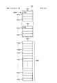
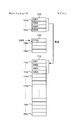
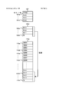
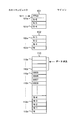
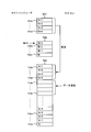
- FIG. 1 It is a figure which shows the aspect by which the backup apparatus of one Embodiment of this invention was connected to the host computer. It is a figure which shows the initial state before storing log data about the work memory and the preservation
- FIG. 1 shows a state in which a backup device 1 according to an embodiment of the present invention is connected to a host computer 2.
- the backup device 1 includes one substrate 1A. On the substrate 1A, a work memory 100, a storage memory 110, an FPGA (Field-Programmable Gate Array) 120 as an interface unit, and a microcomputer (hereinafter abbreviated as “microcomputer”) 130 as a control unit. First to fourth buffers 141, 142, 143, and 144, a battery 150 for backing up the work memory 100, a power-off detector 190, an address bus 161 for designating an address, and data A data bus 162 for transferring and a control signal bus 163 for controlling access are mounted.
- the FPGA 120 includes a contention control unit 121 and a local bridge 122.
- the backup device 1 is connected to a host computer 2.
- the board 1A of the backup device 1 is detachably attached to a motherboard 2A of the host computer 2 via a PCI (Peripheral Component Component) slot (not shown). Therefore, such a one-board type backup device 1 can be easily applied to an existing host computer without requiring a design change of the motherboard of the host computer.
- PCI Peripheral Component Component
- the work memory 100 includes a first work memory 101 composed of one SRAM having a storage capacity of 4 MB and a first SRAM composed of one SRAM having a storage capacity of 4 MB. It consists of two parts in total, with two work memories 102. Since the work memory 100 is composed of SRAM, the log data can be stored in the work memory 100 at a relatively high speed. In addition, since the work memory 100 is divided into two SRAMs, hardware restrictions can be reduced and design flexibility can be increased.
- the memory cells of the first work memory 101 and the second work memory 102 are accessed by specifying addresses.
- the storage areas of the first work memory 101 and the second work memory 102 are divided into four 1 MB storage areas 101a to 101d and 102a to 102d.
- first and second work memories 101 and 102 are backed up by a battery 150 in FIG.
- the work memory 100 is connected to the contention control unit 121 and the local bridge 122 of the FPGA 120 via the address bus 161 and the second buffer 142, while the local address bus 162 and the fourth buffer Are connected to the competition control unit 121 and the microcomputer 130 through the buffer 144.
- the work memory 100 is connected to the local bridge 122 via the data bus 163 and the second buffer 142, and is connected to the microcomputer 130 via the local data bus 164 and the fourth buffer 144. ing. Further, the work memory 100 is connected to the contention control unit 121 via the memory control signal bus 171.
- the storage memory 110 is composed of a NOR flash memory which is a nonvolatile memory having a higher recording density than the work memory 100. Since the storage memory 110 has a higher recording density than the work memory 100, a larger amount of log data can be stored in the storage memory 110. Further, unlike the NAND flash memory, the storage memory 110 does not destroy the configuration of the file management area or the like when the power is interrupted. Therefore, log data can be stored more safely and reliably.
- the work memory 100 is composed of an SRAM that can be backed up by a battery, and the storage memory 110 is composed of a nonvolatile memory. Therefore, even if the power is cut off, the log data can be kept in the work memory 100 or the storage memory 110. For this reason, a large amount of the log data can be stored safely and reliably.
- Each memory cell of the storage memory 110 is accessed by designating an address in the same manner as the first work memory 101 and the second work memory 102.
- the storage area of the storage memory 110 is divided into N storage areas 110a to 110n each having 1 MB.
- N 64, that is, the storage memory 110 has a storage capacity of 64 MB.
- the storage memory 110 is connected to the contention control unit 121 and the local bridge 122 of the FPGA 120 via the address bus 161 and the first buffer 141, similarly to the work memory 100.
- the contention controller 121 and the microcomputer 130 are connected via the local address bus 162 and the third buffer 143.
- the storage memory 110 is connected to the local bridge 122 via the data bus 163 and the first buffer 141, and is connected to the microcomputer 130 via the local data bus 164 and the third buffer 143. Yes. Further, the storage memory 110 is connected to the contention control unit 121 via the memory control signal bus 171.
- the local bridge 122 is connected to the contention control unit 121 via an address bus 161 and a main memory control signal bus 172, while being connected via a PCI bus or a PCI express (registered trademark, hereinafter referred to as PCIe) bus 210. It is connected to a chip set 205 of the host computer 2 described later.
- the local bridge 122 converts the data from the host computer 2 into log data, address information where the log data is to be stored, and an access request to the work memory 100 or the storage memory 110, respectively.
- the local bridge 122 transfers log data to the second buffer 142 via the data bus 163 and transfers address information where the log data is to be stored to the second buffer 142 via the address bus 161. To do.
- the local bridge 122 transfers address information in which log data is to be stored to the contention control unit 121 via the address bus 161, and controls access to the work memory 100 or the storage memory 110 as main memory control. Transfer to the competition control unit 121 via the signal bus 172. Therefore, the host computer 2 can directly access the work memory 100 and the storage memory 110.
- the contention control unit 121 receives the address information where the log data is to be stored and the access request to the work memory 100 or the storage memory 110 from the local bridge 122.
- the contention control unit 121 is connected to the microcomputer 130 via a local address bus 162 and a local memory control signal bus 173. Then, the contention control unit 121 receives from the microcomputer 130 address information where log data should be stored and an access request to the work memory 100 or the storage memory 110.
- the contention control unit 121 is connected to the first and second buffers 141 and 142 via the main buffer control signal bus 174, while the third and fourth buffers are connected via the local buffer control line 175. It is connected to the buffers 143 and 144.
- the contention control unit 121 receives the first to first data based on data received from the local bridge 122 and the microcomputer 130 (address information in which log data is to be stored and access request signals to the work memory 100 or the storage memory 110).
- the fourth buffers 141, 142, 143, and 144 are controlled. Specifically, the contention control unit 121 receives a request for access from the host computer 2 to the work memory 100 or the storage memory 110 and a request from the microcomputer 130 to access the work memory 100 or the storage memory 110. Mediate conflicts.
- the contention control unit 121 permits only one of the host computer 2 and the microcomputer 130 to access the work memory 100 or the storage memory 110 and does not permit access to the other. Therefore, the host computer 2 and the microcomputer 130 can smoothly access the work memory 100 and the storage memory 110, respectively.
- the microcomputer 130 controls the work memory 100 to transfer a part of the log data stored in the work memory 100 to the storage memory 110 for storage. Next, the microcomputer 130 transfers another part of the log data to the storage memory 110 and stores it. In addition, the microcomputer 130 controls the operation of the entire backup device 1.
- the power-off detection unit 190 is connected to the power supply box 3 via the host computer 2 and is connected to the FPGA 120 and the microcomputer 130.
- the power-off detection unit 190 detects the occurrence of power-off of the power supply box 3 based on voltage, and transmits a power-off occurrence signal to the CPU 201 of the host computer 2, the competition control unit 121 of the FPGA 120, and the microcomputer 130. .
- the power-off detection unit 190 may be mounted not on the board 1A of the backup device 1 but on the motherboard 2A of the host computer 2.
- the host computer 2 includes a CPU 201, a main memory 202, a hard disk (not shown), a CF card 203 as a removable disk, a BIOS (Basic Input / Output System), a flash ROM 204, and a chip set. 205 and an internal power conversion unit 206.
- the CPU 201 is connected to the main memory 202 and the chip set 205 via a bus on the mother board 2A.
- the chip set 205 is connected to the CF card 203 and the BIOS / flash / ROM 204 via the bus, and to the local bridge 122 of the backup device 1 via the PCI bus or the PCIe bus 210 as described above. Has been.
- While the internal power conversion unit 206 is connected to the power supply box 3, as shown in FIG. 1, the work memory 100, the storage memory 110, the FPGA 120, the microcomputer 130, the first memory of the backup device 1 Through the fourth buffer 141, 142, 143, 144, the CPU 201 of the host computer 2, the main memory 202, the hard disk and CF card 203, the BIOS / flash ROM 204, and the chip set 205.
- the internal power conversion unit 206 converts the AC power of the power supply box 3 into a DC power and supplies it to each element connected to the backup device 1 and the host computer 2.
- the backup device 1 operates in general with the host computer 2 as follows.
- Log data is transferred from the CPU 201 to the local bridge 122 via the chip set 205 under the control of the CPU 201. Then, the log data is converted by the local bridge 122, and address information in which the log data is to be stored and a signal for requesting access to the work memory 100 are transferred to the contention control unit 121.
- the contention control unit 121 Upon receiving the address information where the log data should be stored and the signal requesting access to the work memory 100 from the CPU 201, the contention control unit 121 requests access from the microcomputer 130 to the work memory 100 or the storage memory 110. Determine if there is any.
- the contention control unit 121 controls the second buffer 142 to allow the CPU 201 to access the work memory 100.
- the contention control unit 121 performs contention control and controls the second buffer 142 immediately or after a predetermined time has elapsed.
- the CPU 201 permits access to the work memory 100 from the CPU 201.
- the log data and the address information where the log data is to be stored are transferred from the local bridge 122 to the work memory 100, and the log data is stored at a predetermined address in the work memory 100.
- the speed at which the log data is stored in the work memory 100 that is, the writing speed is relatively high, and is substantially the same as the transfer speed of the log data from the CPU 201 to the work memory 100. Therefore, the log data can be smoothly transferred from the work memory 100 to the storage memory 110 and stored.
- the address information where the log data should be stored and the work memory 100 are stored.
- a signal requesting access is transmitted from the microcomputer 130 to the contention control unit 121.
- the contention control unit 121 Upon receiving the address information where the log data is to be stored and the signal requesting access to the work memory 100 from the microcomputer 130, the contention control unit 121 requests access from the CPU 201 to the work memory 100 or the storage memory 110. Determine if there is any.
- the contention control unit 121 controls the fourth buffer 144 to permit the microcomputer 130 to access the work memory 100.
- the contention control unit 121 performs contention control and controls the fourth buffer 144 immediately or after a predetermined time has elapsed. Access from the microcomputer 130 to the work memory 100 is permitted. Then, the microcomputer 130 transfers address information in which log data is to be stored in the work memory 100 and reads predetermined log data from the work memory 100.
- the contention control unit 121 For the predetermined log data, under the control of the microcomputer 130, address information where the log data is to be stored and a signal requesting access to the storage memory 110 are transmitted from the microcomputer 130 to the contention control unit 121. Upon receiving the address information where the predetermined log data is to be stored and a signal requesting access to the storage memory 110 from the microcomputer 130, the contention control unit 121 transfers the work information to the work memory 100 or the storage memory 110 from the CPU 201. It is determined whether there is an access request. When determining that there is no access request to the storage memory 110 from the CPU 201, the contention control unit 121 controls the third buffer 143 to permit access from the microcomputer 130 to the storage memory 110.
- the contention control unit 121 performs contention control and controls the third buffer 143 immediately or after a predetermined time elapses. Access from the microcomputer 130 to the work memory 100 is permitted. Then, the microcomputer 130 transfers the predetermined log data and address information where the log data is to be stored to the storage memory 110 and stores the predetermined log data at a predetermined address in the storage memory 110. .
- the backup device 1 operates as follows when it detects the occurrence of power interruption.
- the power-off detection unit 190 transmits a power supply abnormality signal to the FPGA 120 and the microcomputer 130 when the occurrence of power-off of the power supply box 3 is detected by voltage.
- the contention control unit 121 operates as a cutoff control unit, and transmits a memory access stop signal to the work memory 100 and the storage memory 110 via the memory control signal bus 171. To do.
- the work memory 100 and the storage memory 110 receive the memory access stop signal, the work memory 100 and the storage memory 110 cannot be accessed.
- the FPGA 120 issues a power failure interrupt to the CPU 201.
- the CPU 201 stops access to the work memory 100 and the storage memory 110 and waits for the power to drop.
- the microcomputer 130 receives the power supply abnormality signal, the microcomputer 130 stops access to the work memory 100 and the storage memory 110 and waits for the power supply to drop.
- storage in the storage memory 110 that is, log data storage processing when the log data has a size of 64 MB, for example, will be described in detail using the memory maps of FIGS.
- log data (64 MB) to be stored consists of “0001”, “0002”,..., “N”.
- the first work memory 101, the second work memory 102, and the storage memory 110 are in a state where no log data is stored. is there.
- a release flag (F00) that indicates release is written in the start address of the first storage area 101a of the first work memory 101 and the start address of the start storage area 102a of the second work memory 102, respectively.
- the first addresses (several bytes) of the first and second work memories 101 and 102 are reserved for flags, and log data is not written.
- log data “0001”, “0002”, “0003”, and “0004” transferred from the CPU 201 of the host computer 2 are stored in the four storage areas 101 a to 101 d of the first work memory 101 at the head.
- the data is stored sequentially from the storage area 101a in the order of addresses.
- the storage areas 101a to 101d of the first work memory 101 are filled with log data “0001”, “0002”, “0003”, and “0004”, then the log data “0005” is stored.
- ”,“ 0006 ”,“ 0007 ”, and“ 0008 ” are sequentially stored in the four storage areas 102 a to 102 d of the second work memory 102 in the order of addresses from the top storage area 102 a.
- the microcomputer 130 transfers the log data “0001”, “0002”, “0003”, “0004” stored in the first work memory 101 to the storage memory 110 and stores the data in the storage memory 110.
- the areas 110a to 110d are sequentially stored in the order of addresses from the top storage area 110a.
- the microcomputer 130 stores the log data in the first work memory 101.
- the completion flag FF00 is written in the storage area 101a storing the oldest log data “0001”.
- the log data “0008” is stored in the storage area 102 d at the end of the second work memory 102.
- the microcomputer 130 It is confirmed whether or not the completion flag FF00 is written in the first storage area 101a of the first work memory 101. If it is determined that the completion flag is written in the first storage area 101a of the first work memory 101, the log data “0009” is overwritten and stored in this storage area 101a. On the other hand, the microcomputer 130 transfers the log data “0005”, “0006”, “0007”, “0008” stored in the second work memory 102 to the storage memory 110 and stores the data in the storage memory 110.
- the areas 110e to 110h are sequentially stored in the order of addresses from the top storage area 110e.
- the log data transferred from the CPU 201 of the host computer 2 is stored in the first work memory 101 and the second work memory 102 by the ring buffer method. Overwrite the old ones in order.
- the microcomputer 130 (i) saves all the log data stored in the first work memory 101 as described above when all the storage areas 101a to 101d of the first work memory 101 are overwritten. The data is transferred to the memory 110 and stored sequentially in the order of addresses.
- the microcomputer 130 (ii) saves all the log data stored in the second work memory 102 as described above when all the storage areas 102a to 102d of the second work memory 102 are overwritten. The data is transferred to the memory 110 and stored sequentially in the order of addresses.
- the microcomputer 130 sequentially repeats (i) and (ii) above. Therefore, the log data can be efficiently transferred from the work memory 100 to the storage memory 110 and stored.
- the microcomputer 130 erases the oldest log data “0001”, “0002”, “0003”, “0004” among the log data stored in the storage memory 110, and stores the data in the storage memory 110.
- the storage areas 110a to 110d are emptied.
- the microcomputer 130 transfers the log data “N + 1”, “N + 2”, “N + 3”, “N + 4” stored in the first work memory 101 to the storage memory 110, and the storage memory 110 is vacant.
- the storage areas 110a to 110d are sequentially stored in the order of addresses from the top storage area 110a.
- the microcomputer 130 erases the oldest log data “0005”, “0006”, “0007”, “0008” from the log data stored in the storage area of the storage memory 110, and saves the memory 110 storage areas 110e to 110h are emptied.
- the log data is stored by sequentially erasing and rewriting the oldest log data stored in the storage memory 110 by the ring buffer method.
- the power interruption detection unit 190 detects the power interruption, and transmits a power interruption occurrence signal to the CPU 201 of the host computer 2, the competition control unit 121 of the FPGA 120, and the microcomputer 130.
- the CPU 201 and the microcomputer 130 receive the power-off occurrence signal, the CPU 201 and the microcomputer 130 stop accessing the work memory or the storage memory 110 before the power-off occurs.
- the contention control unit 121 serving as the shut-off control unit controls the first to fourth buffers 141, 142, 143, and 144, and works. Control to block access to the memory 100 or the storage memory 110 is performed.
- log data “0001”, “0002”, “0003”, and “0004” are saved from the first work memory 101 to the storage memory 110. If it is in the middle of the transfer to the microcomputer 130, the microcomputer 130 writes a transfer halfway flag informing the fact that the transfer is in progress to a predetermined location in the work memory 100. For example, the transfer-in-progress flag FFF0 is written to the top address of the top storage area 101a of the first work memory 101. After returning from the power interruption, the microcomputer 130 functions as a transfer state detection unit and detects the transfer halfway flag FFF0 written in the work memory 100, and the transfer log data stored in the storage memory 110 is stored.
- the microcomputer 130 again transfers the log data “0001”, “0002”, “0003”, and “0004” of the first work memory 101 to the storage memory 110 and stores them. For this reason, even if the transfer is in the middle of the transfer when the power is cut off, the other part of the log data remaining untransferred in the work memory 100 when the power is turned off is stored in the storage memory 110. Can be reliably transferred to. Therefore, a large amount of the log data can be stored more safely and reliably.
- the microcomputer 130 When the power interruption occurs, for example, as shown in FIG. 7, the microcomputer 130 is in the process of erasing the log data “0001”, “0002”, “0003”, “0004” in the storage memory 110. In this case, the microcomputer 130 writes an erasing flag indicating that the log data was being erased to a predetermined location in the work memory 100. For example, the erasing flag FFFF is written to the top address (address following the completion flag) of the top storage area 101a of the first work memory 101.
- the microcomputer 130 detects the erasure in progress flag FFFF written in the work memory 100 after returning from the power interruption, the erasure log data “0001”, “0002”, “0003” in the storage memory 110 is detected. , “0004” is deleted again. For this reason, even if the log data is being erased when the power is cut off, the log data remaining in the storage memory 110 without being erased can be reliably erased when the power is restored from the power cut.
- the backup device 1 can be realized with a relatively small size and low cost by using commercially available parts, and space and UPS costs can be omitted as compared with the case where a UPS is provided.
- the work memory 100 is composed of SRAM that can be backed up by the battery 150, but in the present invention, it may be composed of FeRAM.
- the backup device 1 is mounted on the board 1A, and the board 1A is detachably attached to the motherboard 2A of the host computer 2.
- the backup computer 1 It may be mounted on the motherboard 2A.
- the configuration of the backup device can be reduced as a whole together with the mother board.
- the release flag F00, the completion flag FF00, the transfer halfway flag FFF0, and the erasure halfway flag FFFF are written in the work memory 100.
- these flags may be written in the SRAM by providing an SRAM different from the work memory 100.
- the storage memory 110 is a NOR flash memory.
- NOR flash memory NOR flash memory
- a NAND flash memory or an SD card memory may be used.
- the FPGA 120 is used as the interface unit.
- an ASIC Application Specific Integrated Circuit
- the microcomputer 130 is used as the control unit.
- an FPGA may be used.
Landscapes
- Engineering & Computer Science (AREA)
- Theoretical Computer Science (AREA)
- Quality & Reliability (AREA)
- Physics & Mathematics (AREA)
- General Engineering & Computer Science (AREA)
- General Physics & Mathematics (AREA)
- Techniques For Improving Reliability Of Storages (AREA)
Abstract
バックアップ装置(1)は、格納したデータがバッテリバックアップされうるSRAMからなるワーク用メモリ(100)と、ワーク用メモリ(100)よりも記録密度が高い不揮発性メモリからなる保存用メモリ(110)とを備える。また、ホストコンピュータ(2)からインターフェイス部(120)を介してワーク用メモリ(100)に転送されて格納されたログデータを保存用メモリ(110)に転送して格納する制御を行うマイコン(130)を備える。
Description
この発明は、コンピュータが作成するログデータのバックアップを行うバックアップ装置およびバックアップ装置の動作方法に関する。
従来、コンピュータを安全に動作させるために、コンピュータに無停電電源装置(UPS:Uninterruptible Power Supply)が付設される場合がある(特開2009-3789号公報、図2(特許文献1))。コンピュータは、商用電源から電源供給を受け、UPSは商用電源から充電用の電源供給を受けている。商用電源の停電(以下「電源断」という。)が発生したときは、UPSが内蔵するバッテリがコンピュータ等の電源となって電気を供給することによって、コンピュータが作成するログデータを安全かつ確実に保存することができる。
しかしながら、上記UPSを設けた場合、ログデータを安全かつ確実に保存できる一方、UPSが一般に大型であるため、設置スペースの確保が難しく、また、UPSのコストが高いという問題がある。
ここで、コンピュータが作成したバックアップすべきログデータが小容量(例えば4MB以下)であれば、例えば、バッテリバックアップされたSRAMを用いる方式によって、小型かつ低コストでログデータを保存できる。しかしながら、一般的に言って、SRAMは1個当たりの記憶容量が比較的少ない。このため、単にSRAMを用いる方式では、バックアップすべきログデータが大容量(数十MB)になると、SRAMの数(部品数)が増えて大型化し、かつ高コストになる。
そこで、この発明の課題は、大容量のログデータを安全かつ確実に保存することができると共に、小型かつ低コストで実現できるバックアップ装置を提供することにある。
上記課題を解決するため、この発明のバックアップ装置は、
格納したデータがバッテリバックアップされうるSRAMからなるワーク用メモリと、
上記ワーク用メモリよりも記録密度が高い不揮発性メモリからなる保存用メモリと、
ホストコンピュータと上記ワーク用メモリ及び上記保存用メモリとの間に介在し、上記ホストコンピュータによる上記ワーク用メモリ及び上記保存用メモリへのアクセスを許容するインターフェイス部と、
上記ホストコンピュータから上記インターフェイス部を介して上記ワーク用メモリに転送されて格納されたログデータを、上記保存用メモリに転送して格納する制御を行う制御部と
を備えることを特徴とする。
格納したデータがバッテリバックアップされうるSRAMからなるワーク用メモリと、
上記ワーク用メモリよりも記録密度が高い不揮発性メモリからなる保存用メモリと、
ホストコンピュータと上記ワーク用メモリ及び上記保存用メモリとの間に介在し、上記ホストコンピュータによる上記ワーク用メモリ及び上記保存用メモリへのアクセスを許容するインターフェイス部と、
上記ホストコンピュータから上記インターフェイス部を介して上記ワーク用メモリに転送されて格納されたログデータを、上記保存用メモリに転送して格納する制御を行う制御部と
を備えることを特徴とする。
この発明のバックアップ装置では、大容量のログデータを次のようにして格納する。上記ホストコンピュータは、上記インターフェイス部を介して、上記ワーク用メモリに大容量のログデータの一部を転送する。上記制御部は、上記ワーク用メモリを制御して、上記ログデータの上記一部を上記保存用メモリに転送して格納する。次に、上記制御部は、上記ログデータの別の一部を上記保存用メモリに転送して格納する。このように、上記制御部は、上記ログデータの一部を順次上記保存用メモリに転送して、格納する。上記ワーク用メモリはSRAMからなるため、上記ログデータを上記ワーク用メモリに比較的高速に格納できる。一方、上記保存用メモリは上記ワーク用メモリよりも記録密度が高いため、より大容量のログデータを上記保存用メモリに格納できる。
また、上記ワーク用メモリは、バッテリバックアップされうるSRAMからなると共に、上記保存用メモリは、不揮発性メモリからなる。したがって、電源断が発生しても、上記ログデータを上記ワーク用メモリまたは上記保存用メモリに保持し続けることができる。このため、大容量の上記ログデータを安全かつ確実に保存できる。
また、このバックアップ装置は、市販の部品を用いて比較的小型かつ低コストで実現でき、UPSを設ける場合に比してスペースおよびUPSのコストを省略できる。
なお、保存用メモリを省略して、ログデータをSRAMからなるワーク用メモリのみでバックアップするものとすると、SRAMの数(部品数)が増えて、大型化し高コストになる。一方、ワーク用メモリを省略して、ログデータを保存用メモリのみでバックアップするものとすると、不揮発性メモリからなる保存用メモリは比較的動作速度が遅いため、ログデータを保存用メモリに格納する速度が遅くなる。
一実施形態のバックアップ装置では、
電源断が発生したことを検知する電源断検知部と、
上記電源断検知部が上記電源断を検知したとき、上記ワーク用メモリ及び上記保存用メモリへのアクセスを遮断する制御を行う遮断制御部と、
上記電源断から復帰したとき、上記電源断の発生時に上記ワーク用メモリに格納された上記ログデータの一部が上記保存用メモリへ転送され、上記ログデータのうち他の部分が残っている転送途中の状態であったか否かを検知する転送状態検知部と
を備え、
上記制御部は、上記転送状態検知部が、上記電源断の発生時に上記転送途中の状態であったことを検知したとき、上記ワーク用メモリに未転送で残っている上記ログデータの上記他の部分を上記保存用メモリに転送して格納する制御を行うことを特徴とする。
電源断が発生したことを検知する電源断検知部と、
上記電源断検知部が上記電源断を検知したとき、上記ワーク用メモリ及び上記保存用メモリへのアクセスを遮断する制御を行う遮断制御部と、
上記電源断から復帰したとき、上記電源断の発生時に上記ワーク用メモリに格納された上記ログデータの一部が上記保存用メモリへ転送され、上記ログデータのうち他の部分が残っている転送途中の状態であったか否かを検知する転送状態検知部と
を備え、
上記制御部は、上記転送状態検知部が、上記電源断の発生時に上記転送途中の状態であったことを検知したとき、上記ワーク用メモリに未転送で残っている上記ログデータの上記他の部分を上記保存用メモリに転送して格納する制御を行うことを特徴とする。
この実施形態のバックアップ装置によれば、電源断(商用電源の停電)が発生したとき、上記電源断検知部が上記電源断を検知する。そして、上記遮断制御部が上記保存用メモリへのアクセスを遮断する制御を行う。上記電源断が発生したとき、上記ワーク用メモリに格納された上記ログデータを上記保存用メモリへ転送する過程にあった場合、上記ログデータの上記一部は上記保存用メモリへ転送され、上記ログデータの他の部分は上記ワーク用メモリに未転送で残っている状態(これを「転送途中の状態」と呼ぶ。)となる。上記電源断から復帰したとき、上記転送状態検知部は、上記転送途中の状態であったか否かを検知する。上記制御部は、上記転送状態検知部が、上記転送途中の状態であったことを検知したとき、上記ワーク用メモリに未転送で残っている上記ログデータの上記他の部分を上記保存用メモリに転送して格納する制御を行う。このため、電源断発生時に上記転送途中の状態であったとしても、上記電源断から復帰したとき、上記ワーク用メモリに未転送で残っている上記ログデータの上記他の部分を、上記保存用メモリへ確実に転送できる。したがって、大容量の上記ログデータをより安全かつ確実に保存できる。
一実施形態のバックアップ装置では、上記ワーク用メモリへのアクセスと、上記保存用メモリへのアクセスとの競合を調停する競合制御部を備えることを特徴とする。
この実施形態のバックアップ装置によれば、上記ホストコンピュータおよび上記制御部による上記ワーク用メモリへのアクセスと、上記保存用メモリへのアクセスとの競合を調停するので、上記ホストコンピュータおよび上記制御部が、それぞれ、上記ワーク用メモリおよび上記保存用メモリに円滑にアクセスできる。
一実施形態のバックアップ装置では、上記インターフェイス部はローカルブリッジを含み、このローカルブリッジは、上記ホストコンピュータが有するデータバスと、上記制御部、上記ワーク用メモリ及び上記保存用メモリの間に設けられたデータバスとを接続していることを特徴とする。
この実施形態のバックアップ装置によれば、上記ホストコンピュータのデータバスと、上記制御部、上記ワーク用メモリ及び上記保存用メモリの間に設けられたデータバスとが、上記ローカルブリッジによって接続されているので、上記ホストコンピュータは、上記ワーク用メモリおよび上記保存用メモリへ直接アクセスすることができる。
一実施形態のバックアップ装置では、上記ホストコンピュータのマザーボードに対して着脱可能な基板を備え、上記ワーク用メモリ、上記保存用メモリ、上記インターフェイス部、及び上記制御部は、上記基板上に搭載されていることを特徴とする。
この実施形態のバックアップ装置によれば、上記基板上に上記ワーク用メモリ、上記保存用メモリ、上記インターフェイス部、及び上記制御部が搭載されている。したがって、マザーボードとは別体の1ボード(基板)タイプのバックアップ装置が構成される。このような1ボードタイプのバックアップ装置は、マザーボードの設計変更を要さず、既存のホストコンピュータに容易に装着して適用できる。
一実施形態のバックアップ装置では、上記ワーク用メモリ、上記保存用メモリ、上記インターフェイス部、及び上記制御部は、上記ホストコンピュータのマザーボード上に搭載されていることを特徴とする。
この実施形態のバックアップ装置によれば、上記マザーボード上に上記ワーク用メモリ、上記保存用メモリ、上記インターフェイス部、及び上記制御部が搭載されているので、マザーボードとともにバックアップ装置の構成を全体として小型にすることができる。
一実施形態のバックアップ装置では、上記ワーク用メモリは、上記ホストコンピュータから転送される上記ログデータの転送速度で書き込み可能であることを特徴とする。
この実施形態のバックアップ装置によれば、上記ログデータが上記ホストコンピュータから転送される速度で、上記ログデータを上記ワーク用メモリに書き込むことができるので、上記ログデータを上記ワーク用メモリから上記保存用メモリに円滑に転送して格納できる。
一実施形態のバックアップ装置では、上記ワーク用メモリは、物理的に独立した2つの上記SRAMからなることを特徴とする。
この実施形態のバックアップ装置によれば、上記ワーク用メモリは、物理的に独立した2つの上記SRAMからなるので、ハードウェア的な制約を低減することができて、設計の自由度を上げることができる。
一実施形態のバックアップ装置では、上記保存用メモリは、NOR型フラッシュメモリであることを特徴とする。
この実施形態のバックアップ装置によれば、上記保存用メモリは、NOR型フラッシュメモリからなるので、NAND系と異なり、電断時にファイル管理エリアなどの構成が破壊されることがない。したがって、上記ログデータをより安全かつ確実に保存できる。
この発明のバックアップ装置の動作方法では、上記制御部は、上記ワーク用メモリに格納された上記ログデータの一部を、上記ワーク用メモリの記憶容量の単位で上記保存用メモリに転送して格納する第1の処理と、上記ワーク用メモリに未転送で残っている上記ログデータの別の一部を、上記ワーク用メモリの記憶容量の単位で上記保存用メモリに転送して格納する第2の処理とを少なくとも順次行うことを特徴とする。
この発明のバックアップ装置の動作方法によれば、上記ワーク用メモリに格納された上記ログデータの一部を、上記ワーク用メモリの記憶容量の単位で上記保存用メモリに転送して格納する処理を繰り返すので、上記ログデータを上記ワーク用メモリから上記保存用メモリに効率よく転送して格納できる。
この発明のバックアップ装置は、
FeRAMからなるワーク用メモリと、
上記ワーク用メモリよりも記録密度が高い不揮発性メモリからなる保存用メモリと、
ホストコンピュータと上記ワーク用メモリ及び上記保存用メモリとの間に介在し、上記ホストコンピュータによる上記ワーク用メモリ及び上記保存用メモリへのアクセスを許容するインターフェイス部と、
上記ホストコンピュータから上記インターフェイス部を介して上記ワーク用メモリに転送されて格納されたログデータを、上記保存用メモリに転送して格納する制御を行う制御部と
を備えることを特徴とする。
FeRAMからなるワーク用メモリと、
上記ワーク用メモリよりも記録密度が高い不揮発性メモリからなる保存用メモリと、
ホストコンピュータと上記ワーク用メモリ及び上記保存用メモリとの間に介在し、上記ホストコンピュータによる上記ワーク用メモリ及び上記保存用メモリへのアクセスを許容するインターフェイス部と、
上記ホストコンピュータから上記インターフェイス部を介して上記ワーク用メモリに転送されて格納されたログデータを、上記保存用メモリに転送して格納する制御を行う制御部と
を備えることを特徴とする。
この発明のバックアップ装置では、大容量のログデータを次のようにして格納する。上記ホストコンピュータは、上記インターフェイス部を介して、上記ワーク用メモリに大容量のログデータの一部を転送する。上記制御部は、上記ワーク用メモリを制御して、上記ログデータの上記一部を上記保存用メモリに転送して格納する。次に、上記制御部は、上記ログデータの別の一部を上記保存用メモリに転送して格納する。このように、上記制御部は、上記ログデータの一部を順次上記保存用メモリに転送して、格納する。上記ワーク用メモリはFeRAM(Ferroelectric Random Access Memory)からなるため、上記制御部は、上記ログデータを上記ワーク用メモリに比較的高速に格納できる。一方、上記保存用メモリは上記ワーク用メモリよりも記録密度が高いため、上記制御部は、より大容量のログデータを上記保存用メモリに格納できる。
また、上記ワーク用メモリは、不揮発性メモリであるFeRAMからなると共に、上記保存用メモリは、不揮発性メモリからなる。したがって、電源断が発生しても、上記ログデータを上記ワーク用メモリまたは上記保存用メモリに保持し続けることができる。このため、大容量の上記ログデータを安全かつ確実に保存できる。
また、このバックアップ装置は、市販の部品を用いて比較的小型かつ低コストで実現でき、UPSを設ける場合に比してスペースおよびUPSのコストを省略できる。
なお、保存用メモリを省略して、ログデータをFeRAMからなるワーク用メモリのみでバックアップするものとすると、FeRAMの数(部品数)が増えて、大型化し高コストになる。一方、ワーク用メモリを省略して、ログデータを保存用メモリのみでバックアップするものとすると、不揮発性メモリからなる保存用メモリは比較的動作速度が遅いため、ホストコンピュータからログデータを保存用メモリに格納する速度が遅くなる。
この発明のバックアップ装置によれば、大容量のログデータを安全かつ確実に保存することができると共に、小型かつ低コストで実現できるバックアップ装置を実現できる。
この発明のバックアップ装置の動作方法によれば、ワーク用メモリに格納されたログデータの一部を、ワーク用メモリの記憶容量の単位で保存用メモリに転送して格納する処理を繰り返すので、ログデータをワーク用メモリから保存用メモリに効率良く転送して格納できる。
以下、この発明を図示の実施形態により詳細に説明する。
図1は、この発明の一実施形態のバックアップ装置1がホストコンピュータ2に接続された態様を示している。
上記バックアップ装置1は、1枚の基板1Aを備えている。この基板1A上に、ワーク用メモリ100と、保存用メモリ110と、インターフェイス部としてのFPGA(Field-Programmable Gate Array)120と、制御部としてのマイクロコンピュータ(以後、「マイコン」と略称する)130と、第1乃至第4のバッファ141,142,143,144と、ワーク用メモリ100をバッテリバックアップするためのバッテリ150と、電源断検知部190と、アドレスを指定するアドレスバス161と、データを転送するデータバス162と、アクセスを制御する制御信号バス163とが搭載されている。上記FPGA120は、競合制御部121とローカルブリッジ122とを有している。また、上記バックアップ装置1は、ホストコンピュータ2に接続されている。具体的には、バックアップ装置1の基板1Aが、ホストコンピュータ2のマザーボード2Aに対して図示しないPCI(Peripheral Component Interconnect)スロットを介して着脱可能に取り付けられている。したがって、このような1ボードタイプのバックアップ装置1は、ホストコンピュータのマザーボードの設計変更を要さず、既存のホストコンピュータに容易に適用できる。
上記ワーク用メモリ100は、図2中に示すように、4MBの記憶容量を有する1個のSRAMからなる第1のワーク用メモリ101と、同じく4MBの記憶容量を有する1個のSRAMからなる第2のワーク用メモリ102との、計2個の部品からなっている。ワーク用メモリ100はSRAMからなるため、上記ログデータをワーク用メモリ100に比較的高速に格納できる。また、ワーク用メモリ100を2個のSRAMに分けて構成しているので、ハードウェア的な制約を低減することができて、設計の自由度を上げることができる。
上記第1のワーク用メモリ101、第2のワーク用メモリ102の各メモリセルは、アドレスを指定してアクセスされる。図2では、便宜上、第1のワーク用メモリ101および第2のワーク用メモリ102の記憶領域を、それぞれ1MBの4つの記憶領域101a~101d,102a~102dに区画して示している。
これらの第1,第2のワーク用メモリ101,102は、それぞれ図1中のバッテリ150によってバッテリバックアップされている。図1中に示すように、上記ワーク用メモリ100は、アドレスバス161および第2のバッファ142を介してFPGA120の競合制御部121およびローカルブリッジ122に接続される一方、ローカルアドレスバス162および第4のバッファ144を介して、競合制御部121およびマイコン130に接続されている。また、上記ワーク用メモリ100は、データバス163および第2のバッファ142を介して、ローカルブリッジ122に接続される一方、ローカルデータバス164および第4のバッファ144を介して、マイコン130に接続されている。さらに、上記ワーク用メモリ100は、メモリ制御信号バス171を介して、競合制御部121に接続されている。
一方、上記保存用メモリ110は、ワーク用メモリ100よりも記録密度が高い不揮発性メモリであるNOR型フラッシュメモリからなっている。保存用メモリ110はワーク用メモリ100よりも記録密度が高いため、より大容量のログデータを保存用メモリ110に格納できる。また、保存用メモリ110は、NAND型フラッシュメモリと異なり、電断時にファイル管理エリアなどの構成が破壊されることがない。したがって、ログデータをより安全かつ確実に保存できる。また、ワーク用メモリ100は、バッテリバックアップされうるSRAMからなると共に、保存用メモリ110は、不揮発性メモリからなる。したがって、電源断が発生しても、ログデータをワーク用メモリ100または保存用メモリ110に保持し続けることができる。このため、大容量の上記ログデータを安全かつ確実に保存できる。
上記保存用メモリ110の各メモリセルは、第1のワーク用メモリ101と第2のワーク用メモリ102と同様に、アドレスを指定してアクセスされる。図2では、便宜上、上記保存用メモリ110の記憶領域を、それぞれ1MBのN個の記憶領域110a~110nに区画して示している。この例では、N=64、つまり保存用メモリ110は、64MBの記憶容量を有している。
図1中に示すように、上記保存用メモリ110は、ワーク用メモリ100と同様に、アドレスバス161および第1のバッファ141を介して、FPGA120の競合制御部121およびローカルブリッジ122に接続される一方、ローカルアドレスバス162および第3のバッファ143を介して、競合制御部121およびマイコン130に接続されている。また、上記保存用メモリ110は、データバス163および第1のバッファ141を介してローカルブリッジ122に接続される一方、ローカルデータバス164および第3のバッファ143を介して、マイコン130に接続されている。さらに、上記保存用メモリ110は、メモリ制御信号バス171を介して、競合制御部121に接続されている。
上記ローカルブリッジ122は、アドレスバス161およびメインメモリ制御信号バス172を介して、競合制御部121に接続される一方、PCIバスまたはPCI express(登録商標、以下、PCIeという。)バス210を介して、後述するホストコンピュータ2のチップセット205に接続されている。上記ローカルブリッジ122は、ホストコンピュータ2からのデータを、ログデータと、ログデータが格納されるべきアドレス情報と、ワーク用メモリ100または保存用メモリ110へのアクセス要求とにそれぞれ変換する。そして、上記ローカルブリッジ122は、ログデータをデータバス163を介して第2のバッファ142に転送するとともに、ログデータが格納されるべきアドレス情報をアドレスバス161を介して第2のバッファ142に転送する。また、上記ローカルブリッジ122は、ログデータが格納されるべきアドレス情報をアドレスバス161を介して競合制御部121に転送するとともに、ワーク用メモリ100または保存用メモリ110へのアクセス要求をメインメモリ制御信号バス172を介して競合制御部121に転送する。したがって、ホストコンピュータ2は、ワーク用メモリ100および保存用メモリ110へ直接アクセスすることができる。
上記競合制御部121は、上述したように、ローカルブリッジ122から、ログデータが格納されるべきアドレス情報と、ワーク用メモリ100または保存用メモリ110へのアクセス要求とを受信する。また、上記競合制御部121は、ローカルアドレスバス162と、ローカルメモリ制御信号バス173とを介して、マイコン130に接続されている。そして、上記競合制御部121は、マイコン130からログデータが格納されるべきアドレス情報とワーク用メモリ100または保存用メモリ110へのアクセス要求とを受信する。
また、上記競合制御部121は、メインバッファ制御信号バス174を介して、第1,第2のバッファ141,142に接続される一方、ローカルバッファ制御線175を介して、第3,第4のバッファ143,144に接続されている。上記競合制御部121は、ローカルブリッジ122およびマイコン130から受信したデータ(ログデータが格納されるべきアドレス情報やワーク用メモリ100または保存用メモリ110へのアクセス要求信号)に基づいて、第1乃至第4のバッファ141,142,143,144を制御する。具体的には、上記競合制御部121は、ホストコンピュータ2からワーク用メモリ100または保存用メモリ110へのアクセス要求と、マイコン130からのワーク用メモリ100または保存用メモリ110へのアクセス要求との競合を調停する。上記競合制御部121は、ホストコンピュータ2またはマイコン130のどちらか一方のみ、ワーク用メモリ100または保存用メモリ110へアクセスすることを許可し、他方については、アクセスを許可しない。したがって、ホストコンピュータ2およびマイコン130が、それぞれ、ワーク用メモリ100および保存用メモリ110に円滑にアクセスできる。
上記マイコン130は、ワーク用メモリ100を制御して、ワーク用メモリ100に格納されているログデータの一部を保存用メモリ110に転送して格納する。次に、上記マイコン130は、上記ログデータの別の一部を保存用メモリ110に転送して格納する。その他、マイコン130は、バックアップ装置1全体の動作を制御する。
上記電源断検知部190は、ホストコンピュータ2を経由して、電源ボックス3に接続される一方、FPGA120と、マイコン130とに接続されている。上記電源断検知部190は、電源ボックス3の電源断の発生を電圧によって検知して、ホストコンピュータ2のCPU201と、FPGA120の競合制御部121と、マイコン130とへ電源断の発生信号を送信する。
なお、電源断検知部190は、バックアップ装置1の基板1A上ではなく、ホストコンピュータ2のマザーボード2A上に搭載されていてもよい。
上記ホストコンピュータ2は、図1中に示すように、CPU201と、メインメモリ202と、図示しないハードディスクと、リムーバブルディスクとしてのCFカード203と、BIOS(Basic Input/Output System) フラッシュ ROM204と、チップセット205と、内部電源変換部206とを有している。
上記CPU201は、マザーボード2A上のバスを介して、メインメモリ202とチップセット205とに接続されている。上記チップセット205は、上記バスを介して、CFカード203と、BIOS フラッシュ ROM204に接続されると共に、上述したように、PCIバスまたはPCIeバス210を介して、バックアップ装置1のローカルブリッジ122に接続されている。
上記内部電源変換部206は、電源ボックス3に接続される一方、図1中に示すように、バックアップ装置1のワーク用メモリ100と、保存用メモリ110と、FPGA120と、マイコン130と、第1乃至第4のバッファ141,142,143,144と、ホストコンピュータ2のCPU201と、メインメモリ202と、上記ハードディスクおよびCFカード203と、BIOS フラッシュ ROM204と、チップセット205とに接続されている。上記内部電源変換部206は、電源ボックス3の交流電源を直流電源に変換して、バックアップ装置1およびホストコンピュータ2の接続されている各要素へ供給する。
上記バックアップ装置1はホストコンピュータ2とともに、概略、次のように動作する。
上記CPU201の制御により、ログデータは、CPU201からチップセット205を経由してローカルブリッジ122へ転送される。すると、ログデータは、ローカルブリッジ122で変換されて、ログデータが格納されるべきアドレス情報とワーク用メモリ100へのアクセスを要求する信号とが、競合制御部121へ転送される。競合制御部121は、CPU201からログデータが格納されるべきアドレス情報とワーク用メモリ100へのアクセスを要求する信号とを受信すると、マイコン130からワーク用メモリ100または保存用メモリ110へのアクセス要求があるかどうか判定する。マイコン130からワーク用メモリ100へのアクセス要求がないと判断すると、競合制御部121は、第2のバッファ142を制御して、CPU201からワーク用メモリ100へのアクセスを許可する。一方、マイコン130からもワーク用メモリ100へのアクセス要求がなされていれば、競合制御部121は、競合制御を行って、直ちに、または所定の時間を経過後に第2のバッファ142を制御して、CPU201からワーク用メモリ100へのアクセスを許可する。そして、ローカルブリッジ122からワーク用メモリ100にログデータとログデータが格納されるべきアドレス情報とを転送して、ログデータをワーク用メモリ100内の所定のアドレスに格納する。このとき、ワーク用メモリ100へログデータを格納する速度、つまり書き込み速度は、比較的高速で、CPU201からワーク用メモリ100へのログデータの転送速度と略同じである。したがって、ログデータをワーク用メモリ100から保存用メモリ110に円滑に転送して格納できる。
次に、バックアップのために、ワーク用メモリ100に保存したログデータを保存用メモリ110へ転送するとき、上記マイコン130の制御により、ログデータが格納されるべきアドレス情報とワーク用メモリ100へのアクセスを要求する信号とをマイコン130から競合制御部121へ送信する。競合制御部121は、マイコン130からログデータが格納されるべきアドレス情報とワーク用メモリ100へのアクセスを要求する信号とを受信すると、CPU201からワーク用メモリ100または保存用メモリ110へのアクセス要求があるかどうか判定する。CPU201からワーク用メモリ100へのアクセス要求がないと判断すると、競合制御部121は、第4のバッファ144を制御して、マイコン130からワーク用メモリ100へのアクセスを許可する。一方、CPU201からもワーク用メモリ100へのアクセス要求があると判断すると、競合制御部121は、競合制御を行って、直ちに、または所定の時間を経過後に第4のバッファ144を制御して、マイコン130からワーク用メモリ100へのアクセスを許可する。そして、マイコン130はワーク用メモリ100にログデータが格納されるべきアドレス情報を転送して、ワーク用メモリ100から所定のログデータを読み込む。
上記所定のログデータについて、上記マイコン130の制御により、ログデータが格納されるべきアドレス情報と保存用メモリ110へのアクセスを要求する信号とをマイコン130から競合制御部121へ送信する。競合制御部121は、マイコン130から上記所定のログデータが格納されるべきアドレス情報と保存用メモリ110へのアクセスを要求する信号とを受信すると、CPU201からワーク用メモリ100または保存用メモリ110へのアクセス要求があるかどうか判定する。CPU201から保存用メモリ110へのアクセス要求がないと判断すると、競合制御部121は、第3のバッファ143を制御して、マイコン130から保存用メモリ110へのアクセスを許可する。一方、CPU201からもワーク用メモリ100へのアクセス要求があると判断すると、競合制御部121は、競合制御を行って、直ちに、または所定の時間を経過後に第3のバッファ143を制御して、マイコン130からワーク用メモリ100へのアクセスを許可する。そして、マイコン130は保存用メモリ110に上記所定のログデータと、ログデータが格納されるべきアドレス情報とを転送して、上記所定のログデータを保存用メモリ110内の所定のアドレスに格納する。
バックアップ装置1は、電源断の発生を検知したとき、次のように動作する。
上記電源断検知部190は、電源ボックス3の電源断の発生を電圧によって検知すると、電源異常信号をFPGA120とマイコン130とへ送信する。上記FPGA120が上記電源異常信号を受信すると、競合制御部121は、遮断制御部として働いて、メモリ制御信号バス171を介して、メモリアクセス中止信号をワーク用メモリ100と保存用メモリ110とに送信する。ワーク用メモリ100および保存用メモリ110がメモリアクセス中止信号を受信すると、ワーク用メモリ100および保存用メモリ110へのアクセスができないようになる。
また、上記FPGA120は、CPU201に対して、電源異常割り込みを発行する。上記CPU201は、この電源異常割り込みを受けると、ワーク用メモリ100および保存用メモリ110へのアクセスを中止して、電源が落ちるのを待つ。また、上記マイコン130は、上記電源異常信号を受信すると、ワーク用メモリ100および保存用メモリ110へのアクセスを中止して、電源が落ちるのを待つ。
次に、図2から図8までのメモリマップを用いて、ログデータが、例えば64MBのサイズである場合の、保存用メモリ110への格納、つまりログデータの保存処理について、詳細に説明する。
この例では、格納すべきログデータ(64MB)が、「0001」,「0002」,…,「N」からなるものとする。
図2に示すように、ログデータを格納する前の初期状態では、第1のワーク用メモリ101,第2のワーク用メモリ102,および保存用メモリ110は、ログデータが格納されていない状態にある。また、第1のワーク用メモリ101の先頭の記憶領域101aの先頭アドレスおよび第2のワーク用メモリ102の先頭の記憶領域102aの先頭アドレスには、それぞれ開放を知らせる開放フラグ(F00)が書き込まれている。なお、第1,第2のワーク用メモリ101,102の先頭アドレス(数バイト)は、フラグ用に確保されており、ログデータが書き込まれることはない。
まず、ホストコンピュータ2のCPU201から転送されてきたログデータ「0001」,「0002」,「0003」,「0004」を、第1のワーク用メモリ101の4つの記憶領域101a~101dに、先頭の記憶領域101aから順次アドレス順に格納していく。
図3に示すように、第1のワーク用メモリ101の記憶領域101a~101dがログデータ「0001」,「0002」,「0003」,「0004」で満杯になると、次に、ログデータ「0005」,「0006」,「0007」,「0008」を第2のワーク用メモリ102の4つの記憶領域102a~102dに先頭の記憶領域102aから順次アドレス順に格納していく。一方、マイコン130は、第1のワーク用メモリ101に格納されたログデータ「0001」,「0002」,「0003」,「0004」を保存用メモリ110に転送して、保存用メモリ110の記憶領域110a~110dに、先頭の記憶領域110aから順次アドレス順に格納していく。
次に、図4に示すように、マイコン130は、第1のワーク用メモリ101から保存用メモリ110へのログデータの転送および格納が完了すると、第1のワーク用メモリ101に格納されているログデータのうち、最も古いログデータ「0001」を格納している記憶領域101aに、完了フラグFF00を書き込む。一方、ログデータ「0008」は、第2のワーク用メモリ102の末尾の記憶領域102dに格納される。
次に、図5に示すように、第2のワーク用メモリ102の記憶領域102a~102dがログデータ「0005」,「0006」,「0007」,「0008」で満杯になると、マイコン130は、第1のワーク用メモリ101の先頭の記憶領域101aに完了フラグFF00が書き込まれているかどうか確認する。第1のワーク用メモリ101の先頭の記憶領域101aに完了フラグが書き込まれていると判断すれば、この記憶領域101aに、ログデータ「0009」を上書きして格納する。一方、マイコン130は、第2のワーク用メモリ102に格納されたログデータ「0005」,「0006」,「0007」,「0008」を保存用メモリ110に転送して、保存用メモリ110の記憶領域110e~110hに、先頭の記憶領域110eから順次アドレス順に格納していく。
その後、同様にして、ホストコンピュータ2のCPU201から転送されてきたログデータを、リングバッファ方式により、第1のワーク用メモリ101および第2のワーク用メモリ102に既に格納されているログデータのうち古いものから順次上書きして、格納していく。
一方、上記マイコン130は、(i)第1のワーク用メモリ101の記憶領域101a~101dが全て上書きされると、上述したように第1のワーク用メモリ101に格納されたログデータを全て保存用メモリ110に転送して、順次アドレス順に格納していく。次に、マイコン130は、(ii)第2のワーク用メモリ102の記憶領域102a~102dが全て上書きされると、上述したように第2のワーク用メモリ102に格納されたログデータを全て保存用メモリ110に転送して、順次アドレス順に格納していく。そして、上記マイコン130は、上記(i),(ii)を順次繰り返す。したがって、上記ログデータをワーク用メモリ100から保存用メモリ110に効率よく転送して格納できる。
図6に示すように、保存用メモリ110の記憶領域110a~110nが、ログデータ「0001」,「0002」,…,「N-1」,「N」で満杯になると、図7に示すように、上記マイコン130は、保存用メモリ110に格納されているログデータのうち、最も古いログデータ「0001」,「0002」,「0003」,「0004」を消去して、保存用メモリ110の記憶領域110a~110dを空にする。
図8に示すように、第1のワーク用メモリ101の記憶領域101a~101dにログデータ「N+1」,「N+2」,「N+3」,「N+4」を上書きして格納すると、次に、第2のワーク用メモリ102の先頭の記憶領域102aにログデータ「N+5」を上書きして格納する。一方、マイコン130は、第1のワーク用メモリ101に格納されたログデータ「N+1」,「N+2」,「N+3」,「N+4」を保存用メモリ110に転送して、保存用メモリ110の空いている記憶領域110a~110dに、先頭の記憶領域110aから順次アドレス順に格納していく。そして、マイコン130は、保存用メモリ110の記憶領域に格納されているログデータのうち、最も古いログデータ「0005」,「0006」,「0007」,「0008」を消去して、保存用メモリ110の記憶領域110e~110hを空にする。
このようにして、リングバッファ方式により、保存用メモリ110に既に格納されているログデータのうち古いものから順次消去および書き換えを行って、ログデータを格納していく。
次に、電源断が発生したときのログデータの保障について、説明する。
上記電源断が発生したとき、電源断検知部190が上記電源断を検知して、ホストコンピュータ2のCPU201と、FPGA120の競合制御部121と、マイコン130とへ電源断の発生信号を送信する。そして、上記CPU201とマイコン130とは、上記電源断の発生信号を受信すると、ワーク用メモリまたは保存用メモリ110へのアクセスを上記電源断の発生前に中止する。一方、遮断制御部としての競合制御部121は、電源断検知部190から上記電源断の発生信号を受信すると、第1乃至第4のバッファ141,142,143,144を制御して、ワーク用メモリ100または保存用メモリ110へのアクセスを遮断する制御を行う。
また、上記電源断が発生したときに、例えば、図3に示すように、ログデータ「0001」,「0002」,「0003」,「0004」が第1のワーク用メモリ101から保存用メモリ110への転送途中の状態であった場合、上記マイコン130は、転送途中の状態であったことを知らせる転送途中フラグをワーク用メモリ100中の所定の場所に書き込む。例えば、転送途中フラグFFF0を第1のワーク用メモリ101の先頭の記憶領域101aの先頭アドレスに書き込む。電源断からの復帰後、上記マイコン130は、転送状態検知部として働いて、ワーク用メモリ100に書き込まれた上記転送途中フラグFFF0を検知すると、保存用メモリ110に格納された転送途中のログデータ「0001」,「0002」,「0003」,「0004」を消去する。そして、上記マイコン130は、再度、第1のワーク用メモリ101のログデータ「0001」,「0002」,「0003」,「0004」を保存用メモリ110に転送して、格納する。このため、電源断発生時に転送途中の状態であったとしても、上記電源断から復帰したとき、ワーク用メモリ100に未転送で残っている上記ログデータの上記他の部分を、保存用メモリ110へ確実に転送できる。したがって、大容量の上記ログデータをより安全かつ確実に保存できる。
また、上記電源断が発生したとき、例えば、図7に示すように、上記マイコン130が保存用メモリ110におけるログデータ「0001」,「0002」,「0003」,「0004」を消去途中であった場合、上記マイコン130は、ログデータを消去途中であったことを知らせる消去途中フラグをワーク用メモリ100中の所定の場所に書き込む。例えば、消去途中フラグFFFFを第1のワーク用メモリ101の先頭の記憶領域101aの先頭アドレス(完了フラグに続くアドレス)に書き込む。電源断からの復帰後、上記マイコン130は、ワーク用メモリ100に書き込まれた上記消去途中フラグFFFFを検知すると、保存用メモリ110における消去途中のログデータ「0001」,「0002」,「0003」,「0004」を再度消去する。このため、電源断発生時にログデータを消去途中であったとしても、上記電源断から復帰したとき、保存用メモリ110に消去されずに残っているログデータを確実に消去できる。
このバックアップ装置1は、市販の部品を用いて比較的小型かつ低コストで実現でき、UPSを設ける場合に比してスペースおよびUPSのコストを省略できる。
上記実施形態では、ワーク用メモリ100は、バッテリ150によってバッテリバックアップされうるSRAMからなっていたが、この発明では、FeRAMからなっていてもよい。
また、上記実施形態では、上記バックアップ装置1は、基板1A上に搭載されており、この基板1Aがホストコンピュータ2のマザーボード2Aに着脱可能に取り付けられていたが、この発明では、ホストコンピュータ2のマザーボード2A上に搭載されていてもよい。この場合、マザーボード上にワーク用メモリ、保存用メモリ、インターフェイス部、及び制御部が搭載されるので、マザーボードとともにバックアップ装置の構成を全体として小型にすることができる。
また、上記実施形態では、開放フラグF00、完了フラグFF00、転送途中フラグFFF0、消去途中フラグFFFFをワーク用メモリ100に書き込んだが、これに限られるものではない。例えば、それらのフラグは、ワーク用メモリ100とは別のSRAMを設けて、そのSRAMに書き込んでもよい。
また、上記実施形態では、上記保存用メモリ110は、NOR型フラッシュメモリからなっていたが、この発明では、NAND型フラッシュメモリや、SDカードメモリを使用していてもよい。
また、上記実施形態では、インターフェイス部として、FPGA120を使用していたが、この発明では、ASIC(Application Specific Integrated Circuit)を使用していてもよい。
また、上記実施形態では、制御部として、マイコン130を使用していたが、この発明では、FPGAを使用していてもよい。
1 バックアップ装置
1A 基板
2 ホストコンピュータ
2A マザーボード
100 ワーク用メモリ
101 第1のワーク用メモリ
102 第2のワーク用メモリ
110 保存用メモリ110
120 FPGA
121 競合制御部
122 ローカルブリッジ
130 マイコン
150 バッテリ
161 アドレスバス
162 ローカルアドレスバス
163 データバス
164 ローカルデータバス
171 メモリ制御信号バス
172 メインメモリ制御信号バス
173 ローカルメモリ制御信号バス
190 電源断検知部
210 PCIバスまたはPCIeバス
1A 基板
2 ホストコンピュータ
2A マザーボード
100 ワーク用メモリ
101 第1のワーク用メモリ
102 第2のワーク用メモリ
110 保存用メモリ110
120 FPGA
121 競合制御部
122 ローカルブリッジ
130 マイコン
150 バッテリ
161 アドレスバス
162 ローカルアドレスバス
163 データバス
164 ローカルデータバス
171 メモリ制御信号バス
172 メインメモリ制御信号バス
173 ローカルメモリ制御信号バス
190 電源断検知部
210 PCIバスまたはPCIeバス
Claims (11)
- 格納したデータがバッテリバックアップされうるSRAMからなるワーク用メモリと、
上記ワーク用メモリよりも記録密度が高い不揮発性メモリからなる保存用メモリと、
ホストコンピュータと上記ワーク用メモリ及び上記保存用メモリとの間に介在し、上記ホストコンピュータによる上記ワーク用メモリ及び上記保存用メモリへのアクセスを許容するインターフェイス部と、
上記ホストコンピュータから上記インターフェイス部を介して上記ワーク用メモリに転送されて格納されたログデータを、上記保存用メモリに転送して格納する制御を行う制御部と
を備えることを特徴とするバックアップ装置。 - 請求項1に記載のバックアップ装置において、
電源断が発生したことを検知する電源断検知部と、
上記電源断検知部が上記電源断を検知したとき、上記ワーク用メモリ及び上記保存用メモリへのアクセスを遮断する制御を行う遮断制御部と、
上記電源断から復帰したとき、上記電源断の発生時に上記ワーク用メモリに格納された上記ログデータの一部が上記保存用メモリへ転送され、上記ログデータのうち他の部分が残っている転送途中の状態であったか否かを検知する転送状態検知部と
を備え、
上記制御部は、上記転送状態検知部が、上記電源断の発生時に上記転送途中の状態であったことを検知したとき、上記ワーク用メモリに未転送で残っている上記ログデータの上記他の部分を上記保存用メモリに転送して格納する制御を行うことを特徴とするバックアップ装置。 - 請求項1又は2に記載のバックアップ装置において、
上記ワーク用メモリへのアクセスと、上記保存用メモリへのアクセスとの競合を調停する競合制御部を備えることを特徴とするバックアップ装置。 - 請求項1から3のいずれか1つに記載のバックアップ装置において、
上記インターフェイス部はローカルブリッジを含み、このローカルブリッジは、上記ホストコンピュータが有するデータバスと、上記制御部、上記ワーク用メモリ及び上記保存用メモリの間に設けられたデータバスとを接続していることを特徴とするバックアップ装置。 - 請求項1から4のいずれか1つに記載のバックアップ装置において、
上記ホストコンピュータのマザーボードに対して着脱可能な基板を備え、
上記ワーク用メモリ、上記保存用メモリ、上記インターフェイス部、及び上記制御部は、上記基板上に搭載されていることを特徴とするバックアップ装置。 - 請求項1から4のいずれか1つに記載のバックアップ装置において、
上記ワーク用メモリ、上記保存用メモリ、上記インターフェイス部、及び上記制御部は、上記ホストコンピュータのマザーボード上に搭載されていることを特徴とするバックアップ装置。 - 請求項1から6のいずれか1つに記載のバックアップ装置において、
上記ワーク用メモリは、上記ホストコンピュータから転送される上記ログデータの転送速度で書き込み可能であることを特徴とするバックアップ装置。 - 請求項1から7のいずれか1つに記載のバックアップ装置において、
上記ワーク用メモリは、物理的に独立した2つの上記SRAMからなることを特徴とするバックアップ装置。 - 請求項1から8のいずれか1つに記載のバックアップ装置において、
上記保存用メモリは、NOR型フラッシュメモリであることを特徴とするバックアップ装置。 - 請求項1に記載のバックアップ装置の動作方法であって、
上記制御部は、
上記ワーク用メモリに格納された上記ログデータの一部を、上記ワーク用メモリの記憶容量の単位で上記保存用メモリに転送して格納する第1の処理と、
上記ワーク用メモリに未転送で残っている上記ログデータの別の一部を、上記ワーク用メモリの記憶容量の単位で上記保存用メモリに転送して格納する第2の処理と
を少なくとも順次行うことを特徴とするバックアップ装置の動作方法。 - FeRAMからなるワーク用メモリと、
上記ワーク用メモリよりも記録密度が高い不揮発性メモリからなる保存用メモリと、
ホストコンピュータと上記ワーク用メモリ及び上記保存用メモリとの間に介在し、上記ホストコンピュータによる上記ワーク用メモリ及び上記保存用メモリへのアクセスを許容するインターフェイス部と、
上記ホストコンピュータから上記インターフェイス部を介して上記ワーク用メモリに転送されて格納されたログデータを、上記保存用メモリに転送して格納する制御を行う制御部と
を備えることを特徴とするバックアップ装置。
Applications Claiming Priority (2)
| Application Number | Priority Date | Filing Date | Title |
|---|---|---|---|
| JP2011-132435 | 2011-06-14 | ||
| JP2011132435 | 2011-06-14 |
Publications (1)
| Publication Number | Publication Date |
|---|---|
| WO2012172708A1 true WO2012172708A1 (ja) | 2012-12-20 |
Family
ID=47356731
Family Applications (1)
| Application Number | Title | Priority Date | Filing Date |
|---|---|---|---|
| PCT/JP2011/078511 Ceased WO2012172708A1 (ja) | 2011-06-14 | 2011-12-09 | バックアップ装置およびバックアップ装置の動作方法 |
Country Status (2)
| Country | Link |
|---|---|
| TW (1) | TW201250473A (ja) |
| WO (1) | WO2012172708A1 (ja) |
Cited By (1)
| Publication number | Priority date | Publication date | Assignee | Title |
|---|---|---|---|---|
| JP2016071494A (ja) * | 2014-09-29 | 2016-05-09 | 株式会社バッファロー | 通信装置、通信システム、通信装置における動作方法及びプログラム |
Families Citing this family (3)
| Publication number | Priority date | Publication date | Assignee | Title |
|---|---|---|---|---|
| TWI483105B (zh) * | 2013-01-31 | 2015-05-01 | Hon Hai Prec Ind Co Ltd | 主機板及其備份基板管理控制系統的方法 |
| TWI718317B (zh) * | 2016-11-04 | 2021-02-11 | 南韓商三星電子股份有限公司 | 資料儲存裝置及資料處理系統 |
| CN108021471A (zh) * | 2016-11-04 | 2018-05-11 | 三星电子株式会社 | 数据存储装置、数据处理系统及制造数据存储装置的方法 |
Citations (5)
| Publication number | Priority date | Publication date | Assignee | Title |
|---|---|---|---|---|
| US6571312B1 (en) * | 1999-02-19 | 2003-05-27 | Mitsubishi Denki Kabushiki Kaisha | Data storage method and data processing device using an erasure block buffer and write buffer for writing and erasing data in memory |
| US6795890B1 (en) * | 1999-02-19 | 2004-09-21 | Mitsubishi Denki Kabushiki Kaisha | Data storage method, and data processing device using an erasure block buffer and write buffer for writing and erasing data in memory |
| JP2008097635A (ja) * | 1999-02-19 | 2008-04-24 | Mitsubishi Electric Corp | 情報処理装置 |
| US20080104344A1 (en) * | 2006-10-25 | 2008-05-01 | Norio Shimozono | Storage system comprising volatile cache memory and nonvolatile memory |
| CA2714745A1 (en) * | 2008-02-12 | 2009-08-20 | Netapp, Inc. | Hybrid media storage system architecture |
-
2011
- 2011-12-09 WO PCT/JP2011/078511 patent/WO2012172708A1/ja not_active Ceased
-
2012
- 2012-01-12 TW TW101101176A patent/TW201250473A/zh unknown
Patent Citations (10)
| Publication number | Priority date | Publication date | Assignee | Title |
|---|---|---|---|---|
| US6571312B1 (en) * | 1999-02-19 | 2003-05-27 | Mitsubishi Denki Kabushiki Kaisha | Data storage method and data processing device using an erasure block buffer and write buffer for writing and erasing data in memory |
| US6795890B1 (en) * | 1999-02-19 | 2004-09-21 | Mitsubishi Denki Kabushiki Kaisha | Data storage method, and data processing device using an erasure block buffer and write buffer for writing and erasing data in memory |
| JP2008097635A (ja) * | 1999-02-19 | 2008-04-24 | Mitsubishi Electric Corp | 情報処理装置 |
| US20080104344A1 (en) * | 2006-10-25 | 2008-05-01 | Norio Shimozono | Storage system comprising volatile cache memory and nonvolatile memory |
| JP2008108026A (ja) * | 2006-10-25 | 2008-05-08 | Hitachi Ltd | 揮発性キャッシュメモリと不揮発性メモリとを備えたストレージシステム |
| CA2714745A1 (en) * | 2008-02-12 | 2009-08-20 | Netapp, Inc. | Hybrid media storage system architecture |
| WO2009102425A1 (en) * | 2008-02-12 | 2009-08-20 | Netapp, Inc. | Hybrid media storage system architecture |
| EP2263145A1 (en) * | 2008-02-12 | 2010-12-22 | Netapp, Inc. | Hybrid media storage system architecture |
| US20110035548A1 (en) * | 2008-02-12 | 2011-02-10 | Kimmel Jeffrey S | Hybrid media storage system architecture |
| JP2011515727A (ja) * | 2008-02-12 | 2011-05-19 | ネットアップ,インコーポレイテッド | ハイブリッド媒体ストレージシステムアーキテクチャ |
Cited By (1)
| Publication number | Priority date | Publication date | Assignee | Title |
|---|---|---|---|---|
| JP2016071494A (ja) * | 2014-09-29 | 2016-05-09 | 株式会社バッファロー | 通信装置、通信システム、通信装置における動作方法及びプログラム |
Also Published As
| Publication number | Publication date |
|---|---|
| TW201250473A (en) | 2012-12-16 |
Similar Documents
| Publication | Publication Date | Title |
|---|---|---|
| TWI540583B (zh) | 用於具有非揮發性記憶體之一系統的電力預算的動態分配 | |
| US8527693B2 (en) | Apparatus, system, and method for auto-commit memory | |
| US20190324859A1 (en) | Method and Apparatus for Restoring Data after Power Failure for An Open-Channel Solid State Drive | |
| US7739443B2 (en) | Memory controller, memory device and control method for the memory controller | |
| US20100235568A1 (en) | Storage device using non-volatile memory | |
| CN103678177B (zh) | 固态硬盘装置 | |
| US20160118130A1 (en) | Performance acceleration during shutdown of a data storage device | |
| US12086432B2 (en) | Gradually reclaim storage space occupied by a proof of space plot in a solid state drive | |
| US9582192B2 (en) | Geometry aware block reclamation | |
| CN104272390B (zh) | 包括闪存阵列和ram阵列的组成的存储器阵列且其具有数据写入ram阵列和从闪存阵列读取数据 | |
| TW201839613A (zh) | 數據儲存裝置及其操作方法 | |
| US20170060436A1 (en) | Technologies for managing a reserved high-performance memory region of a solid state drive | |
| CN113711189B (zh) | 用于管理固态驱动器上的降低电力故障能量需求的系统及方法 | |
| CN111414133B (zh) | 操作存储器控制器和存储器系统的方法以及存储器系统 | |
| KR20200032527A (ko) | 메모리 시스템의 동작 방법 및 메모리 시스템 | |
| US20240086076A1 (en) | Systems and methods for using a storage device as persistent memory | |
| US9965017B2 (en) | System and method for conserving energy in non-volatile dual inline memory modules | |
| JP2011018241A (ja) | 退避処理装置、退避処理方法およびストレージシステム | |
| CN109815158A (zh) | 进行系统备份的方法、记忆装置及控制器、及电子装置 | |
| WO2012172708A1 (ja) | バックアップ装置およびバックアップ装置の動作方法 | |
| EP4320508A1 (en) | Method and apparatus to reduce nand die collisions in a solid state drive | |
| US10795772B2 (en) | Memory system | |
| US20240264750A1 (en) | Atomic Operations Implemented using Memory Services of Data Storage Devices | |
| US20190073147A1 (en) | Control device, method and non-transitory computer-readable storage medium | |
| US20130080717A1 (en) | Information processing apparatus and control method |
Legal Events
| Date | Code | Title | Description |
|---|---|---|---|
| 121 | Ep: the epo has been informed by wipo that ep was designated in this application |
Ref document number: 11867634 Country of ref document: EP Kind code of ref document: A1 |
|
| NENP | Non-entry into the national phase |
Ref country code: DE |
|
| 122 | Ep: pct application non-entry in european phase |
Ref document number: 11867634 Country of ref document: EP Kind code of ref document: A1 |
|
| NENP | Non-entry into the national phase |
Ref country code: JP |