WO2012165405A1 - 表示パネルおよびフーリエ変換赤外分光法によるシール剤の硬化状態の検査方法 - Google Patents
表示パネルおよびフーリエ変換赤外分光法によるシール剤の硬化状態の検査方法 Download PDFInfo
- Publication number
- WO2012165405A1 WO2012165405A1 PCT/JP2012/063704 JP2012063704W WO2012165405A1 WO 2012165405 A1 WO2012165405 A1 WO 2012165405A1 JP 2012063704 W JP2012063704 W JP 2012063704W WO 2012165405 A1 WO2012165405 A1 WO 2012165405A1
- Authority
- WO
- WIPO (PCT)
- Prior art keywords
- substrate
- display panel
- seal portion
- metal layer
- absorption spectrum
- Prior art date
- Legal status (The legal status is an assumption and is not a legal conclusion. Google has not performed a legal analysis and makes no representation as to the accuracy of the status listed.)
- Ceased
Links
Images



Classifications
-
- G—PHYSICS
- G02—OPTICS
- G02F—OPTICAL DEVICES OR ARRANGEMENTS FOR THE CONTROL OF LIGHT BY MODIFICATION OF THE OPTICAL PROPERTIES OF THE MEDIA OF THE ELEMENTS INVOLVED THEREIN; NON-LINEAR OPTICS; FREQUENCY-CHANGING OF LIGHT; OPTICAL LOGIC ELEMENTS; OPTICAL ANALOGUE/DIGITAL CONVERTERS
- G02F1/00—Devices or arrangements for the control of the intensity, colour, phase, polarisation or direction of light arriving from an independent light source, e.g. switching, gating or modulating; Non-linear optics
- G02F1/01—Devices or arrangements for the control of the intensity, colour, phase, polarisation or direction of light arriving from an independent light source, e.g. switching, gating or modulating; Non-linear optics for the control of the intensity, phase, polarisation or colour
- G02F1/13—Devices or arrangements for the control of the intensity, colour, phase, polarisation or direction of light arriving from an independent light source, e.g. switching, gating or modulating; Non-linear optics for the control of the intensity, phase, polarisation or colour based on liquid crystals, e.g. single liquid crystal display cells
- G02F1/133—Constructional arrangements; Operation of liquid crystal cells; Circuit arrangements
- G02F1/1333—Constructional arrangements; Manufacturing methods
- G02F1/1339—Gaskets; Spacers; Sealing of cells
-
- G—PHYSICS
- G02—OPTICS
- G02F—OPTICAL DEVICES OR ARRANGEMENTS FOR THE CONTROL OF LIGHT BY MODIFICATION OF THE OPTICAL PROPERTIES OF THE MEDIA OF THE ELEMENTS INVOLVED THEREIN; NON-LINEAR OPTICS; FREQUENCY-CHANGING OF LIGHT; OPTICAL LOGIC ELEMENTS; OPTICAL ANALOGUE/DIGITAL CONVERTERS
- G02F1/00—Devices or arrangements for the control of the intensity, colour, phase, polarisation or direction of light arriving from an independent light source, e.g. switching, gating or modulating; Non-linear optics
- G02F1/01—Devices or arrangements for the control of the intensity, colour, phase, polarisation or direction of light arriving from an independent light source, e.g. switching, gating or modulating; Non-linear optics for the control of the intensity, phase, polarisation or colour
- G02F1/13—Devices or arrangements for the control of the intensity, colour, phase, polarisation or direction of light arriving from an independent light source, e.g. switching, gating or modulating; Non-linear optics for the control of the intensity, phase, polarisation or colour based on liquid crystals, e.g. single liquid crystal display cells
- G02F1/1306—Details
- G02F1/1309—Repairing; Testing
Definitions
- the present invention relates to a display panel and a method for inspecting a cured state of a sealant in a manufacturing process of the display panel.
- a display panel of a flat display generally has a display medium between a pair of substrates.
- the pair of substrates are bonded to each other by a curable resin called a sealant, and a display medium (for example, a liquid crystal layer or an electrophoretic layer) is sealed and held in a gap between the pair of substrates.
- a display medium for example, a liquid crystal layer or an electrophoretic layer
- the element portion including the organic EL layer is protected from the environment by adopting a structure in which the element portion is sealed between a pair of substrates.
- the liquid crystal display panel 200 includes, for example, a TFT substrate 12, a counter substrate 22, and a liquid crystal layer 32 formed between the TFT substrate 12 and the counter substrate 22.
- the TFT substrate 12 and the counter substrate 22 are bonded to each other by a seal portion 42 formed by curing a sealant.
- the seal portion 42 is formed so as to substantially surround the liquid crystal layer 32.
- the sealant is a mixture of a photocurable resin (for example, an ultraviolet curable acrylic resin) and, if necessary, a filler, a granular spacer, and / or conductive particles.
- the sealing agent is drawn in a predetermined pattern on the TFT substrate 12 using a dispenser.
- the sealing agent is a TFT substrate so as to completely surround the pixel formation region (referred to as a TFT substrate region 10D of the liquid crystal display panel) 12D of the TFT substrate 12.
- the sealing agent is applied to the TFT substrate 12 so as to form an injection hole.
- the injection hole is closed by the sealing resin after the TFT substrate 12 and the counter substrate 22 are bonded together, the sealant is cured, and a liquid crystal material is injected between the TFT substrate 12 and the counter substrate 22.
- the seal portion of the liquid crystal display panel includes not only a portion formed by a sealing agent but also a portion formed by a sealing resin that closes the injection hole.
- the area facing the counter substrate 22 (including the pixel formation area 12 ⁇ / b> D) is referred to as a counter area 12 c, and the exposed area not facing the counter substrate 22 is referred to as the end area 12 p.
- a terminal region 13 is formed in the end region 12p of the TFT substrate 12.
- a driving IC is mounted on the terminal region 13. The names of these areas are also used in the description of the present invention.
- a display defect region 10p (for example, a region with low luminance) is observed near the seal portion 42 in the display region 10D. This is considered to be due to the fact that the uncured component in the sealant is dissolved in the liquid crystal material, and the voltage that is effectively applied to the liquid crystal layer is reduced due to interfacial polarization caused by ionic impurities. As time passes, ionic impurities diffuse and the display failure region 10p expands.
- the cured state of the sealant is not directly inspected, but by visual observation of the display unevenness in the lighting inspection of the display panel. That is, in the lighting inspection, when the above-described display unevenness is observed, information that the display unevenness has occurred is transmitted to the substrate bonding process (including the sealing agent curing process). Changes are made.
- Patent Document 1 discloses a method of inspecting a sealant pattern drawn on a substrate by an optical method, but this method cannot inspect the cured state of the sealant.
- an object of the present invention is to provide a method that can be easily introduced into a mass production process of a display panel and can inspect a cured state of a sealant in a nondestructive manner, and a display panel that enables such an inspection.
- a display panel includes a first substrate having an end region and a pixel formation region, and is disposed so as to face the first substrate and to expose the end region of the first substrate.
- the second substrate formed, the display medium layer formed between the first substrate and the second substrate, the first substrate and the second substrate are bonded together, and the pixel formation region is A sealing portion that surrounds, and an additional sealing portion formed of the same material as the sealing portion in the end region of the first substrate, wherein the first substrate has a metal layer under the additional sealing portion. Also have.
- the first substrate has a plurality of wirings and a plurality of electrodes, and the metal layer is separated from the plurality of wirings and the plurality of electrodes.
- the metal layer is formed of the same material as any of the plurality of wirings and the plurality of electrodes.
- the additional seal portion is in direct contact with the metal layer.
- the seal portion is made of an ultraviolet curable acrylic resin.
- An inspection method includes a step of forming the seal portion and the additional seal portion by curing a sealant.
- the process a which acquires the reflected infrared absorption spectrum of a part,
- the process b which evaluates the hardening state of the said sealing agent based on the acquired said reflected infrared absorption spectrum of the said additional seal
- the step b includes a step b1 of comparing a reflection infrared absorption spectrum of the sealing agent prepared in advance in a well-cured state with the reflection infrared absorption spectrum of the additional seal portion.
- the embodiment of the present invention it is possible to directly inspect the cured state of the sealing agent as early as possible before the lighting inspection of the display panel, and the method for inspecting the cured state of the display panel and the sealing agent. Is provided.
- FIG. 4 is a schematic cross-sectional view near an end region 12p of the liquid crystal display panel 100A.
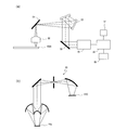
- A) And (b) is a schematic diagram which shows the structure of the apparatus which acquires the reflected infrared absorption spectrum of an additional seal
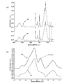
- A) and (b) show the reflected infrared absorption spectrum (OK) of the sealant in a well-cured state and the reflected infrared absorption spectrum (NG) of the sealant in a poorly cured state.
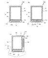
- (A) to (c) are schematic plan views of liquid crystal display panels 100B, 100C, and 100D according to other embodiments of the present invention.
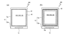
- (A) And (b) is a figure for demonstrating the problem resulting from the hardening defect of the sealing agent in the conventional liquid crystal display panel 200.
- FIG. 1A and 1B schematically show the structure of a liquid crystal display panel 100A according to an embodiment of the present invention.
- FIG. 1A is a schematic plan view of the liquid crystal display panel 100A
- FIG. 1B is a schematic cross-sectional view in the vicinity of the end region 12p of the liquid crystal display panel 100A.
- the liquid crystal display panel 100 ⁇ / b> A includes a first substrate 12, a second substrate 22, and a display medium layer 32 formed between the first substrate 12 and the second substrate 22.
- the first substrate 12 is the TFT substrate 12
- the second substrate 22 is the counter substrate 22
- the display medium layer 32 is the liquid crystal layer 32.
- Each of the TFT substrate 12 and the counter substrate 22 has a glass substrate and necessary components formed on the glass substrate.
- the TFT substrate 12 has a plurality of TFTs, a plurality of wirings connected to the plurality of TFTs, and a plurality of pixel electrodes.
- the counter substrate has a color filter layer and a black matrix (light shielding layer). Since these structures are well known, description thereof is omitted.
- the TFT substrate 12 has an end region 12p and a pixel formation region 12D.
- a terminal region 13a is formed in the end region 12p of the TFT substrate 12, and the pixel formation region 12D becomes the display region 10D of the liquid crystal display panel 100A.
- the counter substrate 22 is disposed so as to face the counter region 12 c of the TFT substrate 12 and expose the end region 12 p of the TFT substrate 12.
- the TFT substrate 12 and the counter substrate 22 are bonded to each other by a seal portion 42a formed so as to surround the pixel formation region 12D.
- the TFT substrate 12 further includes an additional seal portion 44a formed of the same material as the seal portion 42a in the end region 12p, and a metal layer 14a under the additional seal portion 44a.
- the liquid crystal display panel 100A is a liquid crystal display panel manufactured by a dropping injection method, and the liquid crystal layer 32 is formed in an area (display area 10D) surrounded by the seal portion 42a.
- the metal layer 14a and the additional seal portion 44a formed on the metal layer 14a are formed in the end region 12p of the TFT substrate 12. Therefore, when infrared rays (IR) are irradiated from the counter substrate 22 of the liquid crystal display panel 100A, the infrared rays are directly incident on the additional seal portion 44a and pass through the additional seal portion 44a, as indicated by the dashed arrow, and then the metal Reflected at the interface between the layer 14a and the additional seal 44a. By analyzing the reflected infrared absorption spectrum, it is possible to inspect the cured state of the sealing agent forming the additional seal portion 44a.
- IR infrared rays
- the curing state of the sealant forming the additional seal portion 44a can be inspected by so-called reflection FT-IR (Fourier transform infrared spectroscopy).
- reflection FT-IR Fastier transform infrared spectroscopy
- the glass substrate which the counter substrate 22 has absorbs infrared rays strongly when it passes through a glass substrate, the intensity
- a plastic substrate is used instead of the glass substrate.
- the configuration of a spectroscope used for the reflection FT-IR method will be described later.
- the metal layer 14a forms, for example, any of a plurality of wirings (for example, a gate bus line and a source bus line) and a plurality of electrodes (a gate electrode, a source electrode, and terminal electrodes thereof) included in the TFT substrate 12. It can be formed of the same metal material as the metal material. However, the metal layer 14a is preferably separated from the wiring and electrodes (including the wiring and electrodes of the terminal region 13a) of the TFT substrate 12. Since the metal layer 14a is only covered with the additional seal portion 44a, it may not be sufficiently insulated. Therefore, if the wiring or the like is connected to the metal layer 14a, the wiring or the like may not be sufficiently insulated.
- the material for forming the metal layer 14a is, for example, tantalum (Ta), molybdenum (Mo), titanium (Ti), copper (Cu), or aluminum (Al). These metals have a sufficiently high reflectance for infrared rays.
- the metal layer 14a may have a single layer structure or a laminated structure.
- the metal layer 14a can be formed by the same process as the wiring and the like included in the TFT substrate 12. Therefore, the metal layer 14a can be formed only by changing the pattern of a mask for forming a certain wiring in the current manufacturing process, for example.
- the thickness of the metal layer 14a is not particularly limited. When the metal layer 14a is formed by the same process as the wiring or the like, it may have the same thickness as the wiring or the like.
- the thickness of the metal layer 14a is, for example, 100 nm to 500 nm.
- the size of the metal layer 14a depends on the detection optical system and the FT-IR spectrometer (the size of the detector). ⁇ 50 ⁇ m.
- a wiring or the like is covered with an insulating layer (for example, a gate insulating layer, a passivation layer, and / or an interlayer insulating layer).
- the metal layer 14a is preferably in direct contact with the additional seal portion 44a. If an insulating layer (for example, a SiN x layer, a SiO 2 layer, or an organic insulating layer) is present between the metal layer 14a and the additional seal portion 44a, infrared rays are transmitted through the insulating layer. The infrared absorption spectrum of the insulating layer is superimposed on the spectrum.
- the infrared absorption spectrum of the insulating layer becomes a noise for the infrared absorption spectrum of the additional seal portion 44a, and the infrared absorption spectrum of the additional seal portion 44a may not be analyzed with high accuracy. Therefore, the insulating layer formed after forming the metal layer 14a is preferably patterned so as to have an opening or the like that exposes the metal layer 14a. Even if a natural oxide film is formed on the surface of the metal layer 14a, it does not adversely affect the analysis of the infrared absorption spectrum of the additional seal portion 44a if it is sufficiently thin. When forming the alignment film on the TFT substrate 12, it is preferable not to form the alignment film on the metal layer 14a.
- the additional seal portion 44a can be formed by the same process using the same sealant as the seal portion 42a.
- the seal portion is formed by applying a sealant to a predetermined position on a certain substrate using a dispenser or the like, and then bonding the other sealant to the other substrate and curing the sealant.
- the continuous application of the sealing agent to a predetermined position on the substrate sometimes means drawing a seal pattern using the sealing agent.
- the seal part 42a and the additional seal part 44a are formed as follows, for example.
- a seal pattern (which will later become the seal portion 42a) is drawn so as to surround the pixel formation region 12D. Continuously, before or after this, a seal pattern (including a portion that will later become an additional seal portion 44a) is drawn so as to cover the metal layer 14a of the end region 12p.
- FIG. 1A shows an example in which the seal portion 42a and the additional seal portion 44a are connected, the present invention is not limited to this. That is, the additional seal part 44a may be separated from the seal part 42a.
- the seal pattern is preferably continuous so that the amount of the sealant discharged from the dispenser per unit time is constant (so that the width of the seal pattern is constant).
- a liquid crystal material is dropped on the pixel formation region 12D of the TFT substrate 12 on which a predetermined seal pattern is drawn. Thereafter, after the TFT substrate 12 and the counter substrate 22 separately manufactured are bonded together, for example, a sealant containing an ultraviolet curable acrylic resin is irradiated with a predetermined amount of ultraviolet rays. On the contrary, the liquid crystal material may be dropped on the region of the counter substrate 22 that faces the pixel formation region 12D of the TFT substrate 12. Instead of evaluating the cured state of the seal portion 42a, the cured state of the additional seal portion 44a is evaluated, so the additional seal portion 44a is formed by the same process and conditions as the seal portion 42a.
- the reflected infrared absorption spectrum of the additional seal portion 44a is obtained from the counter substrate 22 side using the metal layer 14a, and the cured state of the sealant is obtained based on the obtained reflected infrared absorption spectrum of the additional seal portion 44a.
- FIG. 2A and 2 (b) are schematic diagrams showing the configuration of an apparatus that acquires the reflected infrared absorption spectrum of the additional seal portion 44a.
- the reflected infrared absorption spectrum of the additional seal portion 44a of the liquid crystal display panel 100A is measured using an FT-IR spectrometer 51.
- Infrared light emitted from the FT-IR spectroscope 51 is condensed on the metal layer 14a (see FIG. 2B) of the liquid crystal display panel 100A via the plane mirror 52, the concave mirror 53, the plane mirror 54, and the Cassegrain mirror 55.
- the Cassegrain mirror 55 has a plurality of concave mirrors, plane mirrors, and apertures, and the infrared rays reflected by the metal layer 14a are detected by the detector of the FT-IR spectrometer 51 ( For example, it leads to an MCT (mercury-cadmium-tellurium) detector 51D.
- MCT linear-cadmium-tellurium
- a Cassegrain mirror 55 having a magnification of 32 times is used.
- the diameter of the infrared beam emitted from the FT-IR spectrometer 51 is about 7 to 8 mm, for example, and the light receiving surface of the detector 51D has an area of, for example, 250 ⁇ m ⁇ 250 ⁇ m.
- the 32 ⁇ Cassegrain mirror 55 is used, reflected infrared light from the 46 ⁇ m ⁇ 46 ⁇ m area of the metal layer 14a enters the entire light receiving surface of the detector 51D.
- the size of the metal layer 14a may be about 50 ⁇ m ⁇ about 50 ⁇ m.
- the reflected infrared absorption spectrum acquired by the FT-IR spectrometer 51 is analyzed by the computer 56.
- a monitor 57 and a storage device 58 are connected to the computer 56, and the reflected infrared absorption spectrum is displayed on the monitor 57 and stored in the storage device 58.
- the cured state of the sealing agent is performed, for example, by comparing the infrared absorption spectrum of a well-cured sealing agent prepared in advance with the acquired reflected infrared absorption spectrum of the additional seal portion 44a.
- the infrared absorption spectrum of the well-cured sealant is stored in the storage device 58, and is compared with the acquired reflected infrared absorption spectrum of the additional seal portion 44a by the computer 56.
- the comparison result can be calculated, for example, by the computer 56 as a match rate of the acquired reflected infrared absorption spectrum of the additional seal portion 44a with the infrared absorption spectrum of the well-cured sealant. Further, the obtained reflected infrared absorption spectrum of the additional seal portion 44a and the infrared absorption spectrum of the well-cured sealant may be displayed on the monitor 57 and judged visually. Or you may display the difference spectrum of the reflected infrared absorption spectrum of the additional seal
- the FT-IR spectrometer 51 As the FT-IR spectrometer 51, Avatar 370 manufactured by Thermo Fisher Scientific Co., Ltd. was used.
- the detector 51D is an MCT detector having a light receiving area of 250 ⁇ m ⁇ 250 ⁇ m.
- the measurement wavelength region was a mid-infrared wavelength region (2.5 ⁇ m to 15 ⁇ m, wave number region: 4000 cm ⁇ 1 to 650 cm ⁇ 1 ).
- the resolution during measurement was 4 cm ⁇ 1 and the number of integrations was 64 times.
- the intensity of infrared rays was an interferogram and was 5 V or more.
- the size of the metal layer 14a was 50 ⁇ m ⁇ 50 ⁇ m, and a Cassegrain mirror 55 having a magnification of 32 times was used.
- the metal layer 14a was formed of the same material (for example, titanium (Ti)) as the source bus line of the TFT substrate 12 at the same time as the source bus line.
- an ultraviolet curable acrylic resin for example, Sekisui Chemical Co., Ltd., product number: SD-28 was used.
- 3 (a) and 3 (b) show the reflected infrared absorption spectrum (OK) of the well-cured sealing agent and the reflected infrared absorption spectrum (NG) of the poorly cured sealing agent.
- the main component is the same and is an acrylic resin (cured product) regardless of whether the cured state is good (OK) or defective (NG).
- the spectra are almost the same. Focusing on wavenumber range of expanded 900 cm -1 ⁇ 740 cm -1 in FIG. 3 (b), the difference between the good state of cure and (OK) and bad (NG) is clearly observed.
- the characteristic absorption peak A that appears in the vicinity of 810 cm ⁇ 1 is attributed to the CH out-of-plane bending vibration of the vinyl group of the acrylate sealant.
- the coincidence ratio of the reflected infrared absorption spectrum (NG) of the poorly cured sealant exemplified here to the reflected infrared absorption spectrum (OK) of the well cured sealant was 91%.
- the coincidence rate was obtained by software “OMNIC” attached to Avatar 370 of Thermo Fisher Scientific Co., Ltd.
- the wave number range for obtaining the coincidence rate was set to 4000 cm ⁇ 1 to 650 cm ⁇ 1 .
- the wave number range (wavelength range) for obtaining the coincidence rate can be appropriately set according to the type of the sealing agent.
- the quality of the effect state can be determined based on the numerical value of the match rate.
- the coincidence rate to be determined as good may be set in advance by examining the presence or absence of display unevenness for samples with different curing states. For example, a good determination is made when the match rate is 95% or more.
- absorption intensity is determined as the peak height from the baseline.
- the value (ratio) of the intensity of the absorption peak A / the intensity of the absorption peak B was 0.24 in the good cure state (OK) and 0.51 in the poor cure state (NG). It can be seen that as the value of the intensity of absorption peak A / the intensity of absorption peak B is closer to 0.24, curing proceeds. For example, this value of 0.26 or less can be determined as good.
- the cured state of the sealing agent can be inspected immediately after the curing step (ultraviolet irradiation step) of the sealing agent is finished.
- the process immediately returns to the curing process of the sealing agent, and an additional curing process (additional ultraviolet irradiation) can be performed.
- additional curing process additional ultraviolet irradiation
- the non-defective product rate can be improved.
- the yield rate can be improved.
- the above inspection method can be easily introduced into a mass production line, and is easy to maintain and manage. Therefore, by improving the non-defective product rate, it is possible to sufficiently absorb the cost of introducing, maintaining, and managing inspection equipment.
- the inspection method of the sealing agent according to the embodiment of the present invention can be discriminated by the above method not only when the sealing agent is cured but also when impurities are mixed in the sealing agent.
- FIG. 5 shows a reflection infrared absorption spectrum of a case where a sealant mixed with grease is cured (NG), a well-cured state where no impurities are mixed (OK), and a grease (impurities) mixed in the sealant.
- the absorption spectrum of NG stretching vibration derived from grease increases in the absorption spectrum of NG.
- the coincidence rate of the absorption spectrum of NG was 68%.
- the presence or absence of impurities may be determined before the sealing agent is cured. Although it is difficult to rework after the sealant is cured, it can be easily reworked before the sealant is cured.
- 6A to 6C are schematic plan views of liquid crystal display panels 100B, 100C, and 100D according to other embodiments of the present invention.
- the metal layers 14b1 and 14b2 are formed at two locations in the end region 12p of the TFT substrate 12, and the additional seal portions 44b1 and 44b2 covering the metal layers 14b1 and 14b2 are formed. It may be provided.
- the additional seal portions 44b1 and 44b2 are preferably formed continuously with the seal portion 42b.
- the metal layers 14b1 and 14b2 are preferably separated from the wiring and electrodes (including the wiring and electrodes of the terminal region 13b) of the TFT substrate 12.
- the metal layers 14c1, 14c2, and 14c3 are formed at three locations in the end region 12p of the TFT substrate 12 to cover the metal layers 14c1, 14c2, and 14c3. Seal portions 44c1, 44c2, and 44c3 may be provided. The additional seal portions 44c1, 44c2, and 44c3 are preferably formed continuously with the seal portion 42c. The metal layers 14c1, 14c2, and 14c3 are preferably separated from the wiring and electrodes (including the wiring and electrodes of the terminal region 13c) of the TFT substrate 12.
- a metal layer 14d1 is formed in the end region 12p1, and the end region 12p1 is formed.
- the metal layer 14d2 may be formed in the partial region 12p2, and additional seal portions 44d1 and 44d2 that cover the metal layers 14d1 and 14d2 may be provided.
- the additional seal portions 44d1 and 44d2 are preferably formed continuously with the seal portion 42d.
- the metal layers 14d1 and 14d2 are preferably separated from the wiring and electrodes (including the wiring and electrodes of the terminal region 13d) of the TFT substrate 12.
- the liquid crystal display panel according to the embodiment of the present invention is not limited to the illustrated one, and can be applied to various liquid crystal display panels.
- the embodiment of the present invention has been described by taking a liquid crystal display panel manufactured by a drop injection method as an example, but the present invention is not limited to this, and can be applied to a liquid crystal display panel manufactured by a vacuum injection method. It can also be applied to other display panels.
- the present invention can be applied to a display panel such as a liquid crystal display panel, an electrophoretic display panel or an organic EL display panel, and an inspection of a cured state of a sealant in a manufacturing process thereof.
- Display area 12 First substrate (TFT substrate) 12c Counter area 12D Pixel formation area 12p End area 13a Terminal area 14a, 14b1, 14b2, 14c1, 14c2, 14c3, 14d1, 14d2 Metal layer 22 Second substrate (counter substrate) 32 Display media layer (liquid crystal layer) 42a, 42b, 42c, 42d Seal part 44a, 44b1, 44b2, 44c1, 44c2, 44c3, 44d1, 44d2 Additional seal part 100A, 100B, 100C, 100D, 200 Liquid crystal display panel
Landscapes
- Physics & Mathematics (AREA)
- Nonlinear Science (AREA)
- Chemical & Material Sciences (AREA)
- Crystallography & Structural Chemistry (AREA)
- General Physics & Mathematics (AREA)
- Optics & Photonics (AREA)
- Mathematical Physics (AREA)
- Liquid Crystal (AREA)
- Investigating Or Analysing Materials By Optical Means (AREA)
Abstract
本発明の実施形態による表示パネル(100A)は、端部領域(12p)と画素形成領域(12D)とを有する第1基板(12)と、第1基板(12)と対向し、かつ、第1基板(12)の端部領域(12p)を露出するように配置された第2基板(22)と、第1基板(12)と第2基板(22)との間に形成された表示媒体層(32)と、第1基板(12)と第2基板(22)とを互いに接着し、且つ、画素形成領域(12D)を包囲するシール部(42a)と、第1基板(12)の端部領域(12p)にシール部(42a)と同じ材料で形成された追加シール部(44a)とを有し、第1基板(12)は、追加シール部(44a)の下に金属層(14a)をさらに有する。表示パネル(100A)では、追加シール部(44a)のシール剤の硬化状態をフーリエ変換赤外分光法によって評価することができる。
Description
本発明は、表示パネルおよび表示パネルの製造プロセスにおいてシール剤の硬化状態を検査する方法に関する。
近年、液晶表示装置に代表されるフラットディスプレイが広く用いられている。フラットディスプレイの表示パネルは、一般に、一対の基板の間に表示媒体を有する。一対の基板は、シール剤と呼ばれる硬化性樹脂によって互いに接着され、一対の基板間の間隙に表示媒体(例えば、液晶層、電気泳動層)が密閉・保持される。有機EL表示パネルでは、有機EL層を含む素子部が一対の基板間で密閉された構造を採用することによって、環境から保護している。
これらの表示パネルにおいて、シール剤の硬化が十分でないと、表示品位の低下や、信頼性の低下をもたらすことがある。
図7(a)および(b)を参照して、従来の液晶表示パネル200におけるシール剤の硬化不良に起因する問題を説明する。
液晶表示パネル200は、例えば、TFT基板12と、対向基板22と、TFT基板12と対向基板22との間に形成された液晶層32とを有する。TFT基板12と対向基板22とは、シール剤を硬化することによって形成されたシール部42によって互いに接着されている。シール部42は、液晶層32を実質的に包囲するように形成されている。
シール剤は、光硬化性樹脂(例えば、紫外線硬化性アクリル樹脂)と、必要に応じて、充填剤、粒状スペーサおよび/または導電性粒子が混合される。シール剤は、例えばTFT基板12に、ディスペンサーを用いて所定のパターンに描画される。滴下注入法で液晶材料を注入する場合、シール剤は、TFT基板12の画素形成領域(液晶表示パネルの表示領域10DとなるTFT基板の領域をいう。)12Dを完全に包囲するようにTFT基板12に付与される。一方、真空注入法で液晶材料を注入する場合、シール剤は、注入孔を形成するようにTFT基板12に付与される。注入孔は、TFT基板12と対向基板22とを貼り合せ、シール剤を硬化し、TFT基板12と対向基板22との間に液晶材料を注入した後で、封止樹脂によって塞がれる。本明細書において、液晶表示パネルのシール部とは、シール剤によって形成された部分だけでなく、封止樹脂によって形成された、注入孔を塞ぐ部分を含むものとする。
TFT基板12の領域の内、対向基板22と対向する領域(画素形成領域12Dを含む)を対向領域12cと呼び、対向基板22と対向せず、露出されている領域を端部領域12pということにする。TFT基板12の端部領域12pには、例えば、端子領域13が形成される。端子領域13には、例えば、駆動用ICが実装される。これらの領域の名称は、本発明の説明にも用いる。
なお、以下では、滴下注入法を用いて液晶材料の注入が行われる液晶表示パネルを例に、従来技術の課題を説明する。滴下注入法では、真空注入法よりもシール剤に起因する不良が発生しやすい。主な理由は、以下の2つである。
(1)シール剤を硬化する前に、シール剤が液晶材料と接触するので、シール剤からの不純物が液晶材料中に溶出しやすい。また、(2)液晶材料を注入した後でシール剤を硬化させるので、シール剤を硬化させる条件を十分に安全側に設定する(例えば紫外線の光量を十二分に増やす)ことが難しい。
液晶表示パネル200において、シール部42を形成するシール剤の硬化が不十分であると、表示むらが発生することがある。具体的には、図7(b)に示すように、表示領域10D内のシール部42の近傍に、表示不良領域10p(例えば輝度が低い領域)が観察される。これは、シール剤中の未硬化成分が液晶材料中に溶け出し、イオン性不純物に起因する界面分極等によって、液晶層に実効的に印加される電圧が低下することによると考えられている。時間の経過とともに、イオン性不純物が拡散し、表示不良領域10pが拡大する。
現在、表示パネルの製造プロセスにおいて、シール剤の硬化状態を直接的に検査することはなされておらず、表示パネルの点灯検査における上記表示むらの目視観察によっている。すなわち、点灯検査において、上記の表示むらが観察された場合、基板の貼り合せ工程(シール剤の硬化工程を含む)に、表示むらが発生したという情報が伝達され、例えば、シール剤の硬化条件の変更が行われる。
現行のプロセスでは、貼り合せが終わってから、点灯検査の結果が、基板の貼り合せ工程にフィードバックされるまでに時間を要する。その結果、フィードバックされた情報を得て、例えばシール剤の硬化条件が変更されるまでの間に、従前の硬化条件で貼り合せ工程を経る基板が出てしまうという問題がある。従って、表示パネルの点灯検査よりも前に、シール剤の硬化状態を直接的に検査することが望ましい。
しかしながら、そのような方法は知られていない。例えば、特許文献1には、基板上に描画したシール剤のパターンを光学的な方法で検査する方法が開示されているが、この方法では、シール剤の硬化状態を検査することはできない。
本発明は、表示パネルの点灯検査よりも前に、シール剤の硬化状態を直接的に検査することを可能にするためになされたものである。特に、本発明は、表示パネルの量産プロセスに導入が容易で、非破壊でシール剤の硬化状態を検査できる方法および、そのような検査を可能とする表示パネルを提供することを目的とする。
本発明の実施形態による表示パネルは、端部領域と画素形成領域とを有する第1基板と、前記第1基板と対向し、かつ、前記第1基板の前記端部領域を露出するように配置された第2基板と、前記第1基板と前記第2基板との間に形成された表示媒体層と、前記第1基板と前記第2基板とを互いに接着し、且つ、前記画素形成領域を包囲するシール部と、前記第1基板の前記端部領域に前記シール部と同じ材料で形成された追加シール部とを有し、前記第1基板は、前記追加シール部の下に金属層をさらに有する。
ある実施形態において、前記第1基板は複数の配線および複数の電極を有し、前記金属層は前記複数の配線および前記複数の電極から分離されている。
ある実施形態において、前記金属層は、前記複数の配線および前記複数の電極のいずれかと同じ材料で形成されている。
ある実施形態において、前記追加シール部は、前記金属層と直接接触している。
ある実施形態において、前記シール部は、紫外線硬化性アクリル樹脂から形成されている。
本発明の実施形態による検査方法は、シール剤を硬化することによって、前記シール部および前記追加シール部を形成する工程を包含する、上記のいずれかの表示パネルの製造プロセスにおいてフーリエ変換赤外分光法によって前記シール剤の硬化状態を検査する方法であって、前記シール部および前記追加シール部を形成する工程の後で、前記第2基板側から、前記金属層を利用して、前記追加シール部の反射赤外線吸収スペクトルを取得する工程aと、取得した前記追加シール部の前記反射赤外線吸収スペクトルに基づいて、前記シール剤の硬化状態を評価する工程bとを包含する。
ある実施形態において、前記工程bは、予め用意された良硬化状態の前記シール剤の反射赤外線吸収スペクトルと、前記追加シール部の前記反射赤外線吸収スペクトルとを比較する工程b1を包含する。
本発明の実施形態によると、表示パネルの点灯検査よりも前のできるだけ早い段階で、シール剤の硬化状態を直接的に検査することを可能とする、表示パネルおよびシール剤の硬化状態の検査方法が提供される。
以下、図面を参照して、本発明の実施形態による表示パネルおよびそのような表示パネルの製造プロセスにおいてシール剤の硬化状態を検査する方法を説明する。以下では、液晶表示パネルおよびその製造プロセスを例示するが、本発明は、例示する実施形態に限られない。
図1(a)および(b)に、本発明の実施形態による液晶表示パネル100Aの構造を模式的に示す。図1(a)は液晶表示パネル100Aの模式的な平面図であり、図1(b)は液晶表示パネル100Aの端部領域12p付近の模式的な断面図である。
液晶表示パネル100Aは、第1基板12と、第2基板22と、第1基板12と第2基板22との間に形成された表示媒体層32とを有する。ここでは、第1基板12はTFT基板12であり、第2基板22は対向基板22であり、表示媒体層32は液晶層32である。TFT基板12および対向基板22はそれぞれ、ガラス基板と、ガラス基板上に形成された必要な構成要素とを有している。TFT基板12は、複数のTFTと、複数のTFTに接続された複数の配線および複数の画素電極を有し、対向基板は、カラーフィルタ層やブラックマトリクス(遮光層)を有している。これらの構造はよく知られているので説明を省略する。
TFT基板12は、端部領域12pと画素形成領域12Dとを有する。TFT基板12の端部領域12pには端子領域13aが形成されており、画素形成領域12Dは、液晶表示パネル100Aの表示領域10Dとなる。対向基板22は、TFT基板12の対向領域12cと対向し、かつ、TFT基板12の端部領域12pを露出するように配置されている。TFT基板12と対向基板22とは、画素形成領域12Dを包囲するように形成されたシール部42aによって互いに接着されている。TFT基板12は、さらに、端部領域12pにシール部42aと同じ材料で形成された追加シール部44aと、追加シール部44aの下に金属層14aを有する。液晶表示パネル100Aは、滴下注入法によって製造される液晶表示パネルであり、シール部42aで包囲された領域(表示領域10D)内に液晶層32が形成される。
図1(b)に示すように、金属層14aおよび金属層14a上に形成された追加シール部44aは、TFT基板12の端部領域12pに形成されている。従って、液晶表示パネル100Aの対向基板22から、赤外線(IR)を照射すると、赤外線は、破線の矢印で示すように、追加シール部44aに直接入射し、追加シール部44aを通過した後、金属層14aと追加シール部44aとの界面で反射される。反射された赤外線吸収スペクトルを分析することによって、追加シール部44aを形成するシール剤の硬化状態を検査することができる。すなわち、いわゆる反射FT-IR(フーリエ変換赤外分光)法で、追加シール部44aを形成するシール剤の硬化状態を検査することができる。なお、対向基板22が有するガラス基板は赤外線を強く吸収するので、ガラス基板を介すると、赤外線吸収スペクトルの強度が著しく低下し、分析精度の低下を招く。これを防止するために、追加シール部44aは、対向基板22が存在しない端部領域12pに設けることが好ましい。ガラス基板に代えてプラスチック基板を用いる場合も同様である。反射FT-IR法に用いられる分光器などの構成については後述する。
金属層14aは、例えば、TFT基板12が有する複数の配線(例えば、ゲートバスライン、ソースバスライン)および複数の電極(ゲート電極、ソース電極、およびこれらの端子電極など)のいずれかを形成する金属材料と同じ金属材料で形成され得る。但し、金属層14aは、TFT基板12が有する配線や電極(端子領域13aの配線や電極を含む)から分離されていることが好ましい。金属層14aは追加シール部44aに覆われているだけなので、十分に絶縁されていないことがある。従って、配線等が金属層14aと接続されていると、配線等が十分に絶縁されないおそれがある。
金属層14aを形成する材料は、例えば、タンタル(Ta)、モリブデン(Mo)、チタン(Ti)、銅(Cu)、アルミニウム(Al)である。これらの金属は、赤外線に対して十分に高い反射率を有している。金属層14aは、単層構造または積層構造を有し得る。金属層14aはTFT基板12が有する配線等と同じプロセスで形成され得る。従って、金属層14aは、現行の製造プロセスにおいて、例えば、ある配線を形成するためのマスクのパターンを変更するだけで形成できる。金属層14aの厚さは特に限定されない。金属層14aを配線等と同じプロセスで形成する場合は、配線等と同じ厚さであってよい。金属層14aの厚さは、例えば、100nm~500nmである。金属層14aの大きさ(TFT基板12の法線方向から見たときの大きさ)は、検出光学系やFT-IR分光器(検出器の大きさ)によるが、後述するように、例えば50μm×50μmである。
一般に、配線等は、絶縁層(例えば、ゲート絶縁層、パッシベーション層、および/または層間絶縁層)で覆われる。しかしながら、金属層14aは、追加シール部44aと直接接触することが好ましい。金属層14aと追加シール部44aとの間に、絶縁層(例えば、SiNx層、SiO2層や有機絶縁層)が存在すると、赤外線が絶縁層を透過するので、追加シール部44aの赤外線吸収スペクトルに絶縁層の赤外線吸収スペクトルが重畳することになる。すなわち、絶縁層の赤外線吸収スペクトルは、追加シール部44aの赤外線吸収スペクトルにとってノイズとなるので、追加シール部44aの赤外線吸収スペクトルを高い精度で解析できなくなることがある。従って、金属層14aを形成した後に形成される絶縁層は、金属層14aを露出する開口部等を有するようにパターニングされることが好ましい。なお、金属層14aの表面に自然酸化膜が形成されても、十分に薄ければ、追加シール部44aの赤外線吸収スペクトルの解析に悪影響を及ぼすことはない。TFT基板12に配向膜を形成する場合、金属層14a上には配向膜を形成しないことが好ましい。
追加シール部44aは、シール部42aと同じシール剤を用いて、同じプロセスで形成され得る。一般に、シール部は、ある基板上の所定の位置に、ディスペンサー等を用いてシール剤を付与した後、他の基板と貼り合せ、シール剤を硬化させることによって形成される。このように、シール剤を基板上の所定の位置に連続的に付与することを、シール剤を用いてシールパターンを描画するということがある。
シール部42aおよび追加シール部44aは例えば以下のようにして形成される。
金属層14aおよび配線等を有するTFT基板12の対向領域12cに、画素形成領域12Dを包囲するようにシールパターン(後にシール部42aとなる。)を描画する。これと連続して、これより前または後に、端部領域12pの金属層14aを覆うようにシールパターン(後に追加シール部44aとなる部分を含む。)を描画する。図1(a)では、シール部42aと追加シール部44aとが繋がっている例を示したが、これに限られない。すなわち、追加シール部44aは、シール部42aから分離されてもよい。但し、ディスペンサーから単位時間当たりに吐出されるシール剤の量が一定するように(シールパターンの幅が一定するように)、シールパターンは連続していることが好ましい。
所定のシールパターンが描画されたTFT基板12の画素形成領域12D上に液晶材料を滴下する。その後、TFT基板12と別途作製された対向基板22とを貼り合せた後、例えば、紫外線硬化性アクリル樹脂を含むシール剤に、所定の光量の紫外線を照射する。これとは逆に、TFT基板12の画素形成領域12Dに対向する、対向基板22の領域に液晶材料を滴下してもよい。シール部42aの硬化状態を評価する代わりに、追加シール部44aの硬化状態を評価するので、追加シール部44aはシール部42aと同じプロセス・条件で形成される。
この後、対向基板22側から、金属層14aを利用して、追加シール部44aの反射赤外線吸収スペクトルを取得し、取得した追加シール部44aの反射赤外線吸収スペクトルに基づいて、シール剤の硬化状態を評価する。
図2(a)および(b)を参照して、液晶表示パネル100Aの追加シール部44a(図2では不図示)の反射赤外線吸収スペクトルを取得する方法および反射赤外線吸収スペクトルに基づいて、シール剤の硬化状態を評価する方法を説明する。
図2(a)および(b)は、追加シール部44aの反射赤外線吸収スペクトルを取得する装置の構成を示す模式図である。図2(a)に模式的に示すように、FT-IR分光器51を用いて、液晶表示パネル100Aの追加シール部44aの反射赤外線吸収スペクトルを測定する。
FT-IR分光器51から出射された赤外線は、平面鏡52、凹面鏡53、平面鏡54、カセグレン鏡55を介して、液晶表示パネル100Aの金属層14a(図2(b)参照)に集光される。カセグレン鏡55は、図2(b)に模式的に示すように、複数の凹面鏡、平面鏡およびアパーチャを有しており、金属層14aで反射された赤外線をFT-IR分光器51の検出器(例えばMCT(水銀-カドミウム-テルル)検出器)51Dに導く。カセグレン鏡55を用いると、微小な領域からの反射赤外線スペクトルを効率よく取得することができる。このような方式はマスキング方式と呼ばれることがある。
カセグレン鏡55として、例えば、倍率が32倍のものを用いる。FT-IR分光器51から出射される赤外線のビーム径は例えば約7~8mmで、検出器51Dの受光面は例えば250μm×250μmの面積を有する。このとき、32倍のカセグレン鏡55を用いると、金属層14aの46μm×46μmの面積からの反射赤外光が、検出器51Dの受光面の全体に入射することになる。従って、この場合、金属層14aの大きさは、約50μm×約50μmであればよい。
FT-IR分光器51で取得された反射赤外線吸収スペクトルは、コンピュータ56によって解析される。コンピュータ56には、モニター57および記憶装置58が接続されており、反射赤外線吸収スペクトルは、モニター57に表示され、また、記憶装置58に格納される。シール剤の硬化状態は、例えば、予め用意された良硬化状態のシール剤の赤外線吸収スペクトルと、取得した追加シール部44aの反射赤外線吸収スペクトルとを比較することによって行われる。良硬化状態のシール剤の赤外線吸収スペクトルは、記憶装置58に格納されており、コンピュータ56によって、取得した追加シール部44aの反射赤外線吸収スペクトルと比較される。比較結果は、例えば、コンピュータ56によって、取得した追加シール部44aの反射赤外線吸収スペクトルの、良硬化状態のシール剤の赤外線吸収スペクトルに対する合致率として算出され得る。また、モニター57に、取得した追加シール部44aの反射赤外線吸収スペクトルと、良硬化状態のシール剤の赤外線吸収スペクトルとを表示し、目視によって判断してもよい。あるいは、コンピュータ56によって求めた、取得した追加シール部44aの反射赤外線吸収スペクトルと、良硬化状態のシール剤の赤外線吸収スペクトルとの差スペクトルを表示させてもよい。
以下に、具体例を示す。
FT-IR分光器51として、サーモフィッシャーサイエンティフィック株式会社のAvatar370を用いた。検出器51Dは、受光面積が250μm×250μmのMCT検出器である。測定波長領域は、中赤外波長領域(2.5μm~15μm、波数域:4000cm-1~650cm-1)とした。良く知られているように、この波長域には、O-H、C-H、C=O、C=C、C-O、ベンゼン環など各振動が吸収ピークとして現れる。測定時の分解能は4cm-1、積算回数は64回とした。赤外線の強度はインターフェログラムで、5V以上とした。
金属層14aの大きさは、50μm×50μmで、倍率が32倍のカセグレン鏡55を用いた。金属層14aは、TFT基板12のソースバスラインと同じ材料(例えばチタン(Ti))でソースバスラインと同時に形成した。シール剤としては、紫外線硬化性アクリル樹脂(例えば、積水化学工業株式会社製、品番:SD-28)を用いた。
図3(a)および(b)に、良硬化状態のシール剤の反射赤外線吸収スペクトル(OK)および硬化不良状態のシール剤の反射赤外線吸収スペクトル(NG)を示す。
図3(a)に示すように、4000cm-1~650cm-1の波数域では、硬化状態の良(OK)、不良(NG)にかかわらず、主成分は同じでアクリル樹脂(硬化物)なので、スペクトルはほぼ同じである。図3(b)に拡大した900cm-1~740cm-1の波数域に着目すると、硬化状態の良(OK)と不良(NG)との差が明確に認められる。810cm-1付近に現れる特徴的な吸収ピークAは、アクリレート系シール剤のビニル基のC-H面外変角振動に帰属される。紫外線硬化性アクリル樹脂は、紫外線の照射によって重合開始剤から発生するフリーラジカルにより連鎖重合反応が引き起こされ、硬化反応過程においてC=C結合、および面外のC-H結合が減少する。しかしながら、C=C結合に帰属される1640cm-1~1620cm-1付近の波数域は、重合反応によって生成する化学結合の吸収ピークや、雰囲気中の水蒸気の吸収がバックグランドに重畳することがあるので、比較的バックグランドの変化の少ない810cm-1付近の吸収ピークを指標として選んだ。
なお、ここで例示した硬化不良状態のシール剤の反射赤外線吸収スペクトル(NG)の、良硬化状態のシール剤の反射赤外線吸収スペクトル(OK)に対する合致率は、91%であった。合致率は、サーモフィッシャーサイエンティフィック株式会社のAvatar370に付属のソフトウェア「OMNIC」で求めた。合致率を求める波数範囲は、4000cm-1~650cm-1に設定した。合致率を求める波数範囲(波長範囲)は、シール剤の種類に応じて適宜設定し得る。
この合致率の数値に基づいて、効果状態の良否を判定することができる。良と判定する合致率は、予め硬化状態が異なる試料について、表示むらの発生の有無を調べるなどして、設定しておけばよい。例えば、合致率が95%以上を良判定とする。
なお、目視で判断する際は、図3(b)に示したように、900cm-1~740cm-1付近を拡大すればよい。もちろん、シール剤の種類に応じて指標とする吸収ピーク(注目する波数域)は適宜変更され得る。
次に、図4を参照して、硬化不良状態のシール剤の反射赤外線吸収スペクトル(NG)および良硬化状態のシール剤の反射赤外線吸収スペクトル(OK)について、硬化状態を定量的に判定するための他の方法を説明する。
図4に示すように、吸収ピークA:810cm-1(C-H面外変角振動)と、吸収ピークB:830cm-1(ベンゼン環面外変角振動)について、それぞれの吸収強度を求める。吸収強度は、ベースラインからのピークの高さとして求める。吸収ピークAの強度/吸収ピークBの強度の値(比率)は、良硬化状態(OK)が0.24で、不良硬化状態(NG)が0.51であった。吸収ピークAの強度/吸収ピークBの強度の値が、0.24に近いほど硬化が進んでいることがわかる。例えば、この値が0.26以下を良判定とすることができる。
このように、本発明の実施形態によると、シール剤の硬化状態の良否を非破壊で、迅速に評価することができる。すなわち、本発明の実施形態によると、シール剤の硬化工程(紫外線照射工程)が終わった直後に、シール剤の硬化状態を検査することができる。硬化不良と判定された場合には、直ちに、シール剤の硬化工程に戻し、追加の硬化処理(追加の紫外線照射)を行うことができる。追加の硬化処理によって、良品が得られれば、良品率を向上させることができる。また、硬化条件の変更等を即座に行うことが可能なので、良品率を向上させることができる。さらに、上記の検査方法は、量産ラインに容易に導入することが可能で、且つ、維持・管理も容易である。従って、良品率を向上することによって、検査用の装置の導入および維持・管理のコストを十分に吸収できる。
また、シール剤を変更する際に、従来は表示パネルの点灯評価によって、良否を判断していたのに対し、本発明の実施形態によるシール剤の検査方法を用いると、その必要がなく、最適な硬化条件などを効率よく決定することができる。
なお、本発明の実施形態によるシール剤の検査方法は、シール剤の硬化状態だけでなく、シール剤に不純物が混在した場合にも、上記の方法で判別することができる。
図5を参照して、シールパターンを描画する工程で、シール剤にグリースが混入した場合について説明する。
図5は、グリースが混入したシール剤を硬化した場合(NG)、不純物の混入の無い良硬化状態(OK)、およびシール剤に混入したグリース(不純物)の反射赤外線吸収スペクトルを示す。
図5の反射赤外線吸収スペクトルを比較すると明らかなように、NGの吸収スペクトルには、グリースに由来するC-H伸縮振動等の吸収ピークが増大している。NGの吸収スペクトルの合致率は68%であった。なお、不純物の混入の有無はシール剤を硬化する前に判定するようにしてもよい。シール剤を硬化した後は、リワークが難しいが、シール剤を硬化する前であれば容易にリワークすることができる。
上述したように、本発明の実施形態によると、シール剤の硬化状態の良否や不純物の混入の有無を非破壊で、迅速に評価することができる。
図6(a)~(c)に、本発明の他の実施形態による液晶表示パネル100B、100C、および100Dの模式的な平面図を示す。
図6(a)に示す液晶表示パネル100Bのように、TFT基板12の端部領域12pの2箇所に金属層14b1および14b2を形成し、金属層14b1および14b2を覆う追加シール部44b1および44b2を設けてもよい。追加シール部44b1および44b2は、シール部42bと連続して形成されることが好ましい。金属層14b1および14b2は、TFT基板12が有する配線や電極(端子領域13bの配線や電極を含む)から分離されていることが好ましい。
また、図6(b)に示す液晶表示パネル100Cのように、TFT基板12の端部領域12pの3箇所に金属層14c1、14c2および14c3を形成し、金属層14c1、14c2および14c3を覆う追加シール部44c1、44c2および44c3を設けてもよい。追加シール部44c1、44c2および44c3は、シール部42cと連続して形成されることが好ましい。金属層14c1、14c2および14c3は、TFT基板12が有する配線や電極(端子領域13cの配線や電極を含む)から分離されていることが好ましい。
さらに、図6(c)に示す液晶表示パネル100Dのように、TFT基板12が直交する2つの辺に端部領域12p1および12p2を有する場合、端部領域12p1に金属層14d1を形成し、端部領域12p2に金属層14d2を形成し、金属層14d1および14d2を覆う追加シール部44d1および44d2を設けてもよい。追加シール部44d1および44d2は、シール部42dと連続して形成されることが好ましい。金属層14d1および14d2は、TFT基板12が有する配線や電極(端子領域13dの配線や電極を含む)から分離されていることが好ましい。
本発明の実施形態による液晶表示パネルは例示したものに限られず、種々の液晶表示パネルに適用され得る。ここでは、滴下注入法によって製造される液晶表示パネルを例に、本発明の実施形態を説明したが、本発明はこれに限られず、真空注入法によって製造される液晶表示パネルにも適用できるし、他の表示パネルにも適用できる。
本発明は、液晶表示パネル、電気泳動表示パネルや有機EL表示パネルなどの表示パネルおよびその製造プロセスにおけるシール剤の硬化状態の検査に適用することができる。
10D 表示領域
12 第1基板(TFT基板)
12c 対向領域
12D 画素形成領域
12p 端部領域
13a 端子領域
14a、14b1、14b2、14c1、14c2、14c3、14d1、14d2 金属層
22 第2基板(対向基板)
32 表示媒体層(液晶層)
42a、42b、42c、42d シール部
44a、44b1、44b2、44c1、44c2、44c3、44d1、44d2 追加シール部
100A、100B、100C、100D、200 液晶表示パネル
12 第1基板(TFT基板)
12c 対向領域
12D 画素形成領域
12p 端部領域
13a 端子領域
14a、14b1、14b2、14c1、14c2、14c3、14d1、14d2 金属層
22 第2基板(対向基板)
32 表示媒体層(液晶層)
42a、42b、42c、42d シール部
44a、44b1、44b2、44c1、44c2、44c3、44d1、44d2 追加シール部
100A、100B、100C、100D、200 液晶表示パネル
Claims (7)
- 端部領域と画素形成領域とを有する第1基板と、
前記第1基板と対向し、かつ、前記第1基板の前記端部領域を露出するように配置された第2基板と、
前記第1基板と前記第2基板との間に形成された表示媒体層と、
前記第1基板と前記第2基板とを互いに接着し、且つ、前記画素形成領域を包囲するシール部と、
前記第1基板の前記端部領域に前記シール部と同じ材料で形成された追加シール部と
を有し、
前記第1基板は、前記追加シール部の下に金属層をさらに有する、表示パネル。 - 前記第1基板は複数の配線および複数の電極を有し、前記金属層は前記複数の配線および前記複数の電極から分離されている、請求項1に記載の表示パネル。
- 前記金属層は、前記複数の配線および前記複数の電極のいずれかと同じ材料で形成されている、請求項2に記載の表示パネル。
- 前記追加シール部は、前記金属層と直接接触している、請求項1から3のいずれかに記載の表示パネル。
- 前記シール部は、紫外線硬化性アクリル樹脂から形成されている、請求項1から4のいずれかに記載の表示パネル。
- シール剤を硬化することによって、前記シール部および前記追加シール部を形成する工程を包含する、請求項1から5のいずれかに記載の表示パネルの製造プロセスにおいてフーリエ変換赤外分光法によって前記シール剤の硬化状態を検査する方法であって、
前記シール部および前記追加シール部を形成する工程の後で、前記第2基板側から、前記金属層を利用して、前記追加シール部の反射赤外線吸収スペクトルを取得する工程aと、
取得した前記追加シール部の前記反射赤外線吸収スペクトルに基づいて、前記シール剤の硬化状態を評価する工程bと
を包含する、検査方法。 - 前記工程bは、予め用意された良硬化状態の前記シール剤の反射赤外線吸収スペクトルと、前記追加シール部の前記反射赤外線吸収スペクトルとを比較する工程b1を包含する、請求項6に記載の検査方法。
Priority Applications (1)
| Application Number | Priority Date | Filing Date | Title |
|---|---|---|---|
| US14/123,380 US20140104559A1 (en) | 2011-06-03 | 2012-05-29 | Display panel and method of inspecting cured state of sealing material based on fourier transform infrared spectroscopy |
Applications Claiming Priority (2)
| Application Number | Priority Date | Filing Date | Title |
|---|---|---|---|
| JP2011-125323 | 2011-06-03 | ||
| JP2011125323 | 2011-06-03 |
Publications (1)
| Publication Number | Publication Date |
|---|---|
| WO2012165405A1 true WO2012165405A1 (ja) | 2012-12-06 |
Family
ID=47259259
Family Applications (1)
| Application Number | Title | Priority Date | Filing Date |
|---|---|---|---|
| PCT/JP2012/063704 Ceased WO2012165405A1 (ja) | 2011-06-03 | 2012-05-29 | 表示パネルおよびフーリエ変換赤外分光法によるシール剤の硬化状態の検査方法 |
Country Status (2)
| Country | Link |
|---|---|
| US (1) | US20140104559A1 (ja) |
| WO (1) | WO2012165405A1 (ja) |
Cited By (1)
| Publication number | Priority date | Publication date | Assignee | Title |
|---|---|---|---|---|
| WO2024214198A1 (ja) * | 2023-04-12 | 2024-10-17 | シャープディスプレイテクノロジー株式会社 | 表示装置、表示装置の検査方法、表示装置の製造方法 |
Citations (2)
| Publication number | Priority date | Publication date | Assignee | Title |
|---|---|---|---|---|
| JP2006171680A (ja) * | 2004-12-17 | 2006-06-29 | Au Optronics Corp | 液晶ディスプレイ |
| WO2011040076A1 (ja) * | 2009-09-30 | 2011-04-07 | シャープ株式会社 | 液晶パネル、液晶表示装置及び封止用樹脂の検査方法 |
-
2012
- 2012-05-29 WO PCT/JP2012/063704 patent/WO2012165405A1/ja not_active Ceased
- 2012-05-29 US US14/123,380 patent/US20140104559A1/en not_active Abandoned
Patent Citations (2)
| Publication number | Priority date | Publication date | Assignee | Title |
|---|---|---|---|---|
| JP2006171680A (ja) * | 2004-12-17 | 2006-06-29 | Au Optronics Corp | 液晶ディスプレイ |
| WO2011040076A1 (ja) * | 2009-09-30 | 2011-04-07 | シャープ株式会社 | 液晶パネル、液晶表示装置及び封止用樹脂の検査方法 |
Cited By (1)
| Publication number | Priority date | Publication date | Assignee | Title |
|---|---|---|---|---|
| WO2024214198A1 (ja) * | 2023-04-12 | 2024-10-17 | シャープディスプレイテクノロジー株式会社 | 表示装置、表示装置の検査方法、表示装置の製造方法 |
Also Published As
| Publication number | Publication date |
|---|---|
| US20140104559A1 (en) | 2014-04-17 |
Similar Documents
| Publication | Publication Date | Title |
|---|---|---|
| US10353234B2 (en) | Liquid crystal display having an opening in a light shielding pattern and method of manufacturing the same | |
| CN101651093B (zh) | 半导体薄膜形成方法和半导体薄膜检查装置 | |
| JP5285151B2 (ja) | 液晶パネル及び液晶パネル検査方法 | |
| US8569697B2 (en) | Liquid crystal panel, liquid crystal display device, and method for inspecting sealing resin | |
| JP5150000B2 (ja) | 液晶表示パネル、液晶表示パネル用基板の検査方法 | |
| WO2012165405A1 (ja) | 表示パネルおよびフーリエ変換赤外分光法によるシール剤の硬化状態の検査方法 | |
| US7630071B2 (en) | Inspecting apparatus for glass substrate | |
| CN105445978A (zh) | Tft阵列基板检测方法 | |
| US20090201456A1 (en) | Liquid crystal display device and inspection method thereof | |
| JP5466303B2 (ja) | 液晶表示パネル用基板、液晶表示パネル、液晶表示パネル用基板の製造方法、及び基板検査方法 | |
| US20090135327A1 (en) | Liquid crystal display device and manufacturing method of liquid crystal display device | |
| KR20060045561A (ko) | 액정 표시 패널 및 그 검사 방법 및 그것에 이용하는 검사장치 | |
| JP4158801B2 (ja) | 液晶パネルの製造方法及び液晶パネル用基板の製造方法 | |
| CN100447549C (zh) | 液晶板的试验方法以及试验装置 | |
| US20230417681A1 (en) | Inspection system and inspection method using the same | |
| Otte et al. | Identification of foreign particles in packages of failed products by application of our modified failure analysis flow | |
| KR20070001434A (ko) | 액정표시장치의 검사장비 및 검사방법 | |
| KR101250234B1 (ko) | 액정표시소자 검사시스템 및 방법, 이를 이용한액정표시소자 제조방법 | |
| WO2021024581A1 (ja) | 液晶表示装置の製造方法及び液晶表示装置 | |
| JP2021026216A (ja) | 液晶表示装置の製造方法及び液晶表示装置 | |
| KR20050037659A (ko) | 액정표시장치 검사 방법 | |
| KR20090065844A (ko) | 칼라필터 결함 검사 장치 및 방법 | |
| KR20050067737A (ko) | 박막트랜지스터 액정표시소자 검사장비 | |
| Hwang et al. | P. 94: A High Sensitivity PDCLC‐based Electro‐optic Modulator for TFT Array Inspector | |
| JP2019144371A (ja) | 液晶装置、液晶装置の製造方法、電子機器 |
Legal Events
| Date | Code | Title | Description |
|---|---|---|---|
| 121 | Ep: the epo has been informed by wipo that ep was designated in this application |
Ref document number: 12792509 Country of ref document: EP Kind code of ref document: A1 |
|
| WWE | Wipo information: entry into national phase |
Ref document number: 14123380 Country of ref document: US |
|
| NENP | Non-entry into the national phase |
Ref country code: DE |
|
| 122 | Ep: pct application non-entry in european phase |
Ref document number: 12792509 Country of ref document: EP Kind code of ref document: A1 |
|
| NENP | Non-entry into the national phase |
Ref country code: JP |