WO2012161187A1 - データ構造、映像送信装置、映像受信装置、表示装置、映像送信方法、記録媒体 - Google Patents
データ構造、映像送信装置、映像受信装置、表示装置、映像送信方法、記録媒体 Download PDFInfo
- Publication number
- WO2012161187A1 WO2012161187A1 PCT/JP2012/063040 JP2012063040W WO2012161187A1 WO 2012161187 A1 WO2012161187 A1 WO 2012161187A1 JP 2012063040 W JP2012063040 W JP 2012063040W WO 2012161187 A1 WO2012161187 A1 WO 2012161187A1
- Authority
- WO
- WIPO (PCT)
- Prior art keywords
- video
- original image
- data
- systems
- data indicating
- Prior art date
- Legal status (The legal status is an assumption and is not a legal conclusion. Google has not performed a legal analysis and makes no representation as to the accuracy of the status listed.)
- Ceased
Links
Images




Classifications
-
- H—ELECTRICITY
- H04—ELECTRIC COMMUNICATION TECHNIQUE
- H04N—PICTORIAL COMMUNICATION, e.g. TELEVISION
- H04N7/00—Television systems
- H04N7/01—Conversion of standards, e.g. involving analogue television standards or digital television standards processed at pixel level
- H04N7/0125—Conversion of standards, e.g. involving analogue television standards or digital television standards processed at pixel level one of the standards being a high definition standard
-
- H—ELECTRICITY
- H04—ELECTRIC COMMUNICATION TECHNIQUE
- H04N—PICTORIAL COMMUNICATION, e.g. TELEVISION
- H04N21/00—Selective content distribution, e.g. interactive television or video on demand [VOD]
- H04N21/20—Servers specifically adapted for the distribution of content, e.g. VOD servers; Operations thereof
- H04N21/23—Processing of content or additional data; Elementary server operations; Server middleware
- H04N21/234—Processing of video elementary streams, e.g. splicing of video streams or manipulating encoded video stream scene graphs
- H04N21/2343—Processing of video elementary streams, e.g. splicing of video streams or manipulating encoded video stream scene graphs involving reformatting operations of video signals for distribution or compliance with end-user requests or end-user device requirements
-
- H—ELECTRICITY
- H04—ELECTRIC COMMUNICATION TECHNIQUE
- H04N—PICTORIAL COMMUNICATION, e.g. TELEVISION
- H04N21/00—Selective content distribution, e.g. interactive television or video on demand [VOD]
- H04N21/40—Client devices specifically adapted for the reception of or interaction with content, e.g. set-top-box [STB]; Operations thereof
- H04N21/41—Structure of client; Structure of client peripherals
- H04N21/422—Input-only peripherals, i.e. input devices connected to specially adapted client devices, e.g. global positioning system [GPS]
- H04N21/42204—User interfaces specially adapted for controlling a client device through a remote control device; Remote control devices therefor
-
- H—ELECTRICITY
- H04—ELECTRIC COMMUNICATION TECHNIQUE
- H04N—PICTORIAL COMMUNICATION, e.g. TELEVISION
- H04N21/00—Selective content distribution, e.g. interactive television or video on demand [VOD]
- H04N21/40—Client devices specifically adapted for the reception of or interaction with content, e.g. set-top-box [STB]; Operations thereof
- H04N21/43—Processing of content or additional data, e.g. demultiplexing additional data from a digital video stream; Elementary client operations, e.g. monitoring of home network or synchronising decoder's clock; Client middleware
- H04N21/433—Content storage operation, e.g. storage operation in response to a pause request, caching operations
- H04N21/4334—Recording operations
-
- H—ELECTRICITY
- H04—ELECTRIC COMMUNICATION TECHNIQUE
- H04N—PICTORIAL COMMUNICATION, e.g. TELEVISION
- H04N21/00—Selective content distribution, e.g. interactive television or video on demand [VOD]
- H04N21/40—Client devices specifically adapted for the reception of or interaction with content, e.g. set-top-box [STB]; Operations thereof
- H04N21/45—Management operations performed by the client for facilitating the reception of or the interaction with the content or administrating data related to the end-user or to the client device itself, e.g. learning user preferences for recommending movies, resolving scheduling conflicts
- H04N21/462—Content or additional data management e.g. creating a master electronic programme guide from data received from the Internet and a Head-end or controlling the complexity of a video stream by scaling the resolution or bit-rate based on the client capabilities
- H04N21/4622—Retrieving content or additional data from different sources, e.g. from a broadcast channel and the Internet
-
- H—ELECTRICITY
- H04—ELECTRIC COMMUNICATION TECHNIQUE
- H04N—PICTORIAL COMMUNICATION, e.g. TELEVISION
- H04N21/00—Selective content distribution, e.g. interactive television or video on demand [VOD]
- H04N21/40—Client devices specifically adapted for the reception of or interaction with content, e.g. set-top-box [STB]; Operations thereof
- H04N21/47—End-user applications
- H04N21/478—Supplemental services, e.g. displaying phone caller identification, shopping application
- H04N21/4788—Supplemental services, e.g. displaying phone caller identification, shopping application communicating with other users, e.g. chatting
Definitions
- the present invention relates to video technology.
- the number of pixels of the current high definition television broadcast (High Definition television: so-called full HD (FHD)) is 1920 ⁇ 1080 (so-called 2K1K).
- FHD full HD
- a video standard with 16 times the number of pixels (so-called ultra-high definition and 8K4K) (Super Hi-Vision SHV is one of them) has been proposed.
- an ultra-high-definition original image is divided into high-definition n-region (n is a plurality) images and transmitted in n systems (single scan / multi-display transmission).
- Method hereinafter referred to as “single scan method”, or an ultra-high definition original image of n (n is a plurality) images having a lower definition than the original image (a so-called thinned image in which pixels are thinned out so as to interpolate each other).
- block scan method block scan / single display transmission method, hereinafter simply referred to as block scan method
- the image receiving apparatus corresponding to the block scan method cannot support the image transmitted by the single scan method.
- the video receiving apparatus corresponding to the system cannot cope with the video transmitted by the block scan system, and it is desired to realize a video receiving apparatus that can support both systems.
- One of the objects of the present invention is to facilitate the realization of a video receiving apparatus that can handle both types.
- the original image is divided into n areas (n is an integer of 2 or more) and transmitted by the first to n-th systems (channels), the first method, and the original image is lower than the original image.
- Content data indicating the contents of the original image and the transmission method are divided into n fine images (n is an integer of 2 or more) and transmitted through the first to n-th systems (channels) as the second method.
- Realization of a video receiving apparatus that can support a single scan method and a block scan method can be facilitated.
- FIG. 1 is a schematic diagram illustrating a configuration example of a video transmission device and a video reception device according to Embodiment 1.
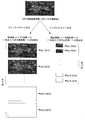
- FIG. It is a schematic diagram explaining a single scan system and a block scan system.
- FIG. 3 is a schematic diagram illustrating block scanning pixel mapping according to the first exemplary embodiment.
- FIG. 3 is a schematic diagram illustrating single scan pixel mapping in the first embodiment.
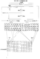
- It is a schematic diagram which shows the position of the auxiliary data in the video data of HDMI transmission.
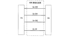
- It is a schematic diagram which shows the structural example in the case of using HDMI for transmission between a video transmission device and a video reception device.
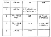
- 6 is a table showing a specific example of auxiliary data (including identification data) in the first embodiment.
- FIG. 6 is a schematic diagram illustrating a configuration example of a video transmission device and a video reception device according to a second embodiment.
- FIG. 10 is a schematic diagram illustrating block scanning pixel mapping in the second embodiment. 10 is a table showing a specific example of auxiliary data (including identification data) in Example 2.
- FIG. 6 is a schematic diagram illustrating a configuration of a liquid crystal display device according to Example 3.
- Example 1 First, as an input (transmission) method of super high-definition video data, a single scan method (see FIG. 2) in which an original image (frame) is divided into 16 region images without changing the definition and transmitted in 16 systems.
- Block scan that divides an original image into 16 images (so-called thinned images in which pixels are thinned out so as to interpolate each other) that are reduced to 1/16 of the original image, and transmits them in n systems
- FIG. 2 shows a method.
- an entire image of 1/16 definition in a state where pixels are thinned out
- the video transmission apparatus ITA divides an original image into 16 frames, and generates a video data generation circuit IGC that generates video data (including content data) of 1st to 16th systems,
- An identification data insertion circuit IAC that inserts identification data indicating a (divided) transmission method into at least one of the first to sixteenth systems of video data, and each of the first to sixteenth systems of video data as differential transmission paths ( For example, the output processing circuit OPC which transmits by TMDS) is included.
- the identification data insertion circuit IAC may be configured to insert the same identification data into all the video data of the first to sixteenth systems.
- the display device DSA includes a video reception device IRA including an input processing circuit IPC, an identification data reading circuit IRC, and a pixel mapping circuit PMC, a display panel DP including four divided display areas DDA1 to DDA4, and 4 And panel drive circuits PD1 to PD4 for driving each of the divided display areas DDA1 to DDA4.
- the display panel DP is, for example, an 8K4K panel (7680 ⁇ 4320 pixels).
- the method of dividing the display panel DP is, for example, a method in which the upper side is divided into two left and right sides and the lower side is divided into two left and right sides (see FIG. 1) There is a method of dividing into four in the left-right direction without dividing into four. For the 8K4K panel, as described later, there is also a method (eight division method) in which the upper side is divided into four in the left-right direction and the lower side is divided into four in the left-right direction.
- the first to sixteenth system video data Qa1 to Qa16 output from the output processing circuit OPC are input in parallel (simultaneously) to the input processing circuit IPC.
- the input processing circuit IPC performs 1st to 16th video data synchronization processing of each pixel data, ⁇ curve correction, color temperature correction, color gamut conversion, etc. for performing panel display suitable for the input video standard.
- the video data (Qb1 to Qb16) are output to the identification data reading circuit IRC.
- the identification data reading circuit IRC reads the identification data from the first to sixteenth system video data, recognizes whether the transmission method of the video data is a single scan method or a block scan method, and transmits the video data Qb1 to Qb16 and the transmission method signal.
- TFS is output to the pixel mapping circuit PMC.
- the pixel mapping circuit PMC rearranges the video data of the first to sixteenth systems according to the transmission method signal TFS and the panel drive method (4-division drive, see FIG. 1) (pixel mapping), and the display control substrates DC1 to DC4. Output to.
- the display control boards DC1 to DC4 control the panel drive circuits PD1 to PD4, respectively. Specifically, for the block scan method, for example, pixel mapping is performed as shown in FIG. 3, and for the single scan method, for example, pixel mapping is performed as shown in FIG.
- FIG. 5 is a schematic diagram showing the input state (for one system) of video data when HDMI (High Definition Multimedia Interface) is used for the input of each of the first to 16th systems.
- an auxiliary data period ADP is provided in the blanking periods (vertical blanking period VBP and horizontal blanking period HBP) other than the video display period IDP.
- VBP and HBP vertical blanking period
- Auxiliary data such as audio data, frame resolution, and number of colors is transmitted. Since the auxiliary data period ADP is provided with an empty area (an area to which specific auxiliary data is not allocated, a reserved area), for example, identification data (flag) may be inserted into this empty area (Japanese Patent Laid-Open No. 2006-2006). -352599 and JP 2005-184441).
- the HDMI transmission path (for one system) between the video transmitting apparatus ITA and the video receiving apparatus IRA includes three data channels (Da-CH0, Da-CH1, Da-CH2), a clock 1 channel (CK-CH), and auxiliary data is packetized and transmitted via three data channels, the contents of which are specified in the Type value (address) of the packet header.
- FIG. 7 is an example of auxiliary data included in the video data of the first embodiment.
- the address indicates a byte address in the auxiliary data.
- identification data indicating a transmission method (single scan method or block scan method) is included as one of auxiliary data.
- the block scan method when the value of auxiliary data at address 0 is 1), Auxiliary data indicating the horizontal size of one block (for example, 8 pixels), auxiliary data indicating the vertical size of one block (for example, 4 lines), and auxiliary data indicating the input system (0 to 15) are included.
- the horizontal size and vertical size of one block are irrelevant, so it is set to 0.
- the auxiliary data of the input system is optional and indicates the position of the pixel data transmitted by each system.
- the pixel mapping circuit PMC can bring the pixel to the correct position even if the input system is not correct (that is, even if 16 cables are mistakenly inserted). However, this is not necessary when the corresponding pixel position is determined for each cable (see Japanese Patent Laid-Open No. 2005-18441).
- the circuit of the input unit of the display can be shared by both input methods, and the circuit scale and cost can be reduced.
- the video recorder only needs to save with one input method, and it can save the recording capacity of HDD (hard disk).
- HDD hard disk
- the original image is divided into 16 sheets and transmitted through the first to 16th systems, but the present invention is not limited to this.
- the video transmission apparatus ITA may divide the original image into four sheets and transmit the first to fourth systems (video data QA1 to QA4).
- the original image is 8K4K size
- the transmission method signal TFS indicates the block scan method
- the pixel mapping circuit PMC for example, as shown in FIG. Perform mapping.
- FIG. 10 is an example of auxiliary data included in the video data of the second embodiment. As shown in FIG. 10, not only auxiliary data indicating the input system (0 to 3) but also auxiliary data indicating the number of inputs (4) may be added.
- Example 3 The liquid crystal display device LCD according to Example 3 is a super high-definition video standard (for example, horizontal 7680 pixels ⁇ vertical 4320 pixels) having a pixel number (8K4K) that is 16 times the number of full HD pixels (horizontal 1920 pixels ⁇ vertical 1080 pixels). As shown in FIG.
- an input processing circuit IPC an identification data reading circuit IRC, a pixel mapping circuit PMC, four display control boards (timing controller boards) DC1 to DC4, a liquid crystal panel LCP, 4 One gate driver GD1 to GD4, two source drivers SD1 to SD2, four CS drivers CD1 to CD4, three power supply devices (not shown) connected to different commercial power sources, a power supply controller (not shown), Backlight BL, backlight driver BLD, and backlight controller A roller BLC is provided.
- the input video signals Qa1 to Qa16 are added with identification data (auxiliary data) that can identify whether the format is a block scan format or a single scan format, and the input processing circuit IPC receives the video signal Qa1.
- auxiliary data auxiliary data
- the input processing circuit IPC receives the video signal Qa1.
- -Qa16 is subjected to the above processing, and video signals Qb1-Qb16 are output to identification data reading circuit IRC.
- the identification data reading circuit IRC reads identification data from the first to sixteenth system video data, recognizes whether the transmission system of the video data is a single scan system or a block scan system, and transmits the transmission system signal TFS to the pixel mapping circuit PMC. Output to.
- the pixel mapping circuit PMC performs pixel mapping according to the transmission method signal TFS.
- the display control board DC1 includes two video processing circuits EP1 and EP2 and two timing controllers TC1 and TC2, and the display control board DC2 includes two video processing circuits EP3 and EP4 and two timing controllers TC3 and TC4.
- the display control board DC3 includes two video processing circuits EP5 and EP6 and two timing controllers TC5 and TC6, and the display control board DC4 includes two video processing circuits EP7 and EP8 and two timing controllers TC7 and TC8. Is provided.
- the pixel mapping circuit PMC generates two video signals (2K2K pixel number) corresponding to the left half AR1 of the local area 1 (upper left region when the liquid crystal panel LCP is divided into four parts in the upper, lower, left and right directions). Divided into signals Qc1 and Qc2) and output to the video processing circuit EP1 of the display control board DC1, and two video signals (2K2K pixels) corresponding to the right half AR2 of the local area 1 (the number of full HD pixels) The video signal Qc3, Qc4) is divided and output to the video processing circuit EP2 of the display control board DC1, and the video corresponding to the left half AR3 of the local area 2 (the upper right area when the liquid crystal panel LCP is divided into four parts vertically and horizontally) The signal (number of 2K2K pixels) is divided into two (video signals Qc5 and Qc6 having the number of full HD pixels) and output to the video processing circuit EP3 of the display control board DC2.
- the video signal (2K2K pixel number) corresponding to the right half AR4 of the local area 2 is divided into two (video signals Qc7 and Qc8 having the number of full HD pixels) and supplied to the video processing circuit EP4 of the display control board DC2. And outputs two video signals (2K2K pixel number) corresponding to the left half AR5 of the local area 3 (lower left region when the liquid crystal panel LCP is divided into four parts vertically and horizontally) (the video signal Qc9 ⁇ Qc10) and output to the video processing circuit EP5 of the display control board DC3, and two video signals (2K2K pixel number) corresponding to the right half AR6 of the local area 3 (the video signal Qc11.
- the video signal (number of 2K2K pixels) corresponding to the left half AR7 is divided into two (video signals Qc13 and Qc14 having the number of full HD pixels) and output to the video processing circuit EP7 of the display control board DC4.
- the video signal corresponding to the right half AR8 (2K2K pixel count) is divided into two (video signals Qc15 and Qc16 having the full HD pixel count) and output to the video processing circuit EP8 of the display control board DC4.
- the pixel mapping circuit PMC outputs a synchronization signal SYS (vertical synchronization signal, horizontal synchronization signal, clock signal, data enable signal, etc.) to the timing controller TC1 of the display control board DC1, and the timing controller TC1 receiving this outputs the synchronization signal SYS.
- This synchronization signal SYS is transmitted to the inter-substrate shared line SSL connected to the display control substrates DC1 to DC4.
- the timing controller TC1 receives the synchronization signal SYS received from the pixel mapping circuit PMC, cooperates with the video processing circuit EP1, performs video processing such as gradation conversion processing on the video signals Qc1 and Qc2, and then supports AR1.
- a source control signal SC1 is output to the source driver substrate (not shown)
- a gate control signal GC1 is output to the gate driver substrate (not shown) of the gate driver GD1
- a CS control signal CC1 is output to the CS driver CD1.
- the timing controller TC2 receives the synchronization signal SYS transmitted from the timing controller TC1 via the inter-substrate shared line SSL, cooperates with the video processing circuit EP2, performs the video processing on the video signals Qc3 and Qc4, and then performs AR2
- a source control signal SC2 is output to a source driver board (not shown) corresponding to
- the timing controller TC3 receives the synchronization signal SYS transmitted from the timing controller TC1 via the inter-substrate shared line SSL, cooperates with the video processing circuit EP3, performs the video processing on the video signals Qc5 and Qc6, and then performs AR3.
- a source control signal SC3 is output to a source driver board (not shown) corresponding to
- the timing controller TC4 receives the synchronization signal SYS transmitted from the timing controller TC1 via the inter-substrate shared line SSL, cooperates with the video processing circuit EP4, performs the video processing on the video signals Qc7 and Qc8, and then performs AR4.
- the source control signal SC4 is output to the source driver board (not shown) corresponding to the above, the gate control signal GC2 is output to the gate driver board (not shown) of the gate driver GD2, and the CS control signal CC2 is sent to the CS driver CD2. Output.
- the timing controller TC5 receives the synchronization signal SYS transmitted from the timing controller TC1 via the inter-substrate shared line SSL, cooperates with the video processing circuit EP5, performs the video processing on the video signals Qc9 and Qc10, and then performs AR5.
- the source control signal SC5 is output to the source driver board (not shown) corresponding to the above, the gate control signal GC3 is output to the gate driver board (not shown) of the gate driver GD3, and the CS control signal CC3 is sent to the CS driver CD3. Output.
- the timing controller TC6 receives the synchronization signal SYS transmitted from the timing controller TC1 via the inter-substrate shared line SSL, cooperates with the video processing circuit EP6, performs the video processing on the video signals Qc11 and Qc12, and then performs AR6.
- a source control signal SC6 is output to a source driver board (not shown) corresponding to
- the timing controller TC7 receives the synchronization signal SYS transmitted from the timing controller TC1 via the inter-substrate shared line SSL, cooperates with the video processing circuit EP7, performs the video processing on the video signals Qc13 and Qc14, and then performs AR7.
- a source control signal SC7 is output to a source driver board (not shown) corresponding to
- the timing controller TC8 receives the synchronization signal SYS transmitted from the timing controller TC1 via the inter-substrate shared line SSL, cooperates with the video processing circuit EP8, performs the video processing on the video signals Qc15 and Qc16, and then performs AR8.
- the source control signal SC8 is output to the source driver board (not shown) corresponding to the above, the gate control signal GC4 is output to the gate driver board (not shown) of the gate driver GD4, and the CS control signal CC4 is sent to the CS driver CD4. Output.
- the source control signals SC1 to SC8 include a data signal, a data latch signal, a source start pulse, and a source clock
- the gate control signals GC1 to GC4 include a gate start pulse and a gate clock.
- the display control boards DC1 to DC4 synchronize their operations by exchanging or sharing various signals between the boards.
- the display control board DC1 which is the master, sends an RDY (ready) signal to the slave display control board DC2, and the display control board DC2 that receives the slave sends the RDY signal to the slave as soon as the preparation is completed.
- the display control board DC3 that has received and received the RDY signal is sent to the slave display control board DC4 as soon as preparation is completed, and the display control board DC4 that has received this is ready. Then, the RDY signal is returned to the display control board DC1.
- the display control board DC1 transmits an operation start (SRST) signal simultaneously to the display control boards DC2 to DC4 via the inter-substrate shared line SSL.
- the timing controller TC1 of the display control board DC1 receives the synchronization signal SYS received from the pixel mapping circuit PMC via the inter-substrate shared line SSL, and the timing controllers TC2 to TC8. Send to all.
- the liquid crystal panel LCP includes an active matrix substrate, a liquid crystal layer (not shown), and a counter substrate (not shown).
- the active matrix substrate includes a plurality of pixel electrodes (not shown) and a plurality of TFTs (thin film transistors, FIG. Scanning signal lines Ga to Gd extending in the row direction (the direction along the long side of the panel), a plurality of data signal lines Sa to Sd extending in the column direction, and a storage capacitor wiring (CS wiring extending in the row direction).
- CSa to CSd and CS trunk wires Ma to Mh extending in the column direction are provided, and a common electrode (not shown), a color filter, and a black matrix (not shown) are provided on the counter substrate. .
- the gate driver GD1 includes a plurality of gate driver chips I provided along one of the two short sides of the upper half of the liquid crystal panel LCP and arranged in the column direction.
- the vertical driver GD2 includes a plurality of gate driver chips I provided along the other of the two short sides of the upper half of the liquid crystal panel LCP and arranged in the column direction.
- the gate driver GD3 includes a plurality of gate driver chips I provided along one of the two short sides of the lower half of the liquid crystal panel LCP and arranged in the column direction.
- the vertical driver GD4 is provided along the other of the two short sides of the lower half of the liquid crystal panel LCP, and includes a plurality of gate driver chips I arranged in the column direction.
- the scanning signal lines provided in the upper half of the panel are driven by the gate drivers GD1 and GD2, and the scanning signal lines provided in the lower half of the panel are driven by the gate drivers GD3 and GD4. That is, one scanning signal line is connected to two gate drivers arranged on both sides thereof, and a scanning (pulse) signal having the same phase is supplied from the two gate drivers to the one scanning signal line. By so doing, it is possible to suppress variations in signal dullness (the degree of signal dullness varies depending on the position in the row direction) caused by CR (time constant) of the scanning signal line.
- the source driver SD1 is provided along one long side of the upper half of the liquid crystal panel LCP, and 48 source driver chips J arranged in the row direction (the number of output terminals of one source driver chip is 960), 4 source driver boards (not shown) are included (12 source driver chips J are mounted on one source driver board).
- the source driver SD2 is provided along one long side of the lower half of the liquid crystal panel LCP, and 48 source driver chips J arranged in the row direction (the number of output terminals of one source driver chip is 960). And four source driver boards (not shown) (12 source driver chips J are mounted on one source driver board).
- Each data signal line provided in the upper half of the panel is driven by the source driver SD1, and each data signal line provided in the lower half of the panel is driven by the source driver SD2.
- the data signal line Sa is driven by the source driver SD1
- the data signal line Sc is driven by the source driver SD2.
- the liquid crystal panel LCP is provided with two data signal lines corresponding to the upper half (first area, upstream side of the panel) of one pixel column, and the lower half (second area, panel of the panel).
- a so-called upper and lower divided double source structure four data signal lines are provided per pixel column, and four scanning signal lines are selected simultaneously, provided with two data signal lines corresponding to the downstream side) 4x speed drive is possible.
- the liquid crystal panel LCP is a so-called multi-pixel method in which at least two pixel electrodes are provided in one pixel, and the viewing angle characteristics can be enhanced by a bright region and a dark region formed in one pixel. ing.
- this data structure is based on the first method in which the original image is divided into n areas (n is an integer of 2 or more) and transmitted in the first to n-th systems, and the original image is obtained from the original image.
- the second method is a method in which the image is divided into n low-definition images (n is an integer of 2 or more) and transmitted through the first to n-th systems, and the content data indicating the contents of the original image and the transmission method are the first method. And identification data indicating the first or second system.
- the identification data may be one of auxiliary data.
- the second method divides the original image into a plurality of blocks each including pixels that are n times the natural number, and distributes pixels that are n times the natural number to the first to nth systems.
- block size data indicating the size of one block may also be included.
- This data structure can also be configured to include system data indicating which of the first to n-th systems is supported.
- each of the n images may include the same number of pixels as the video standard for high-definition television broadcasting.
- the present video transmission apparatus divides an original image into n (n is an integer of 2 or more) regions and transmits the first image to the n-th system in the first method, and the original image has a lower definition than the original image.
- the method of dividing into n (n is an integer of 2 or more) images and transmitting them in the first to n-th systems is the second method, the content data indicating the contents of the original image, and the transmission method is the first or second transmission method. It transmits identification data indicating the system.
- the present video transmission apparatus may be configured such that a differential transmission path is used for each of the first to n-th systems.
- This video receiving apparatus accepts video data having the above data structure.
- the video receiving apparatus can be configured to rearrange the content data according to the transmission method indicated in the identification data.
- This display device includes the above-described video receiving device.
- the original image is divided into n areas (n is an integer of 2 or more) and transmitted by the first to n-th systems in the first method, and the original image is lower in definition than the original image.
- the method of dividing into n (n is an integer of 2 or more) images and transmitting them in the first to n-th systems is the second method, the content data indicating the contents of the original image, and the transmission method is the first or second transmission method. It transmits identification data indicating the system.
- This recording medium is a computer-readable medium on which video data having the above data structure is recorded.
- the present invention is not limited to the above-described embodiments, and those obtained by appropriately modifying the above-described embodiments based on common general technical knowledge and those obtained by combining them are also included in the embodiments of the present invention.
- the present invention is suitable for, for example, an ultra-high definition liquid crystal display device.
- DSA display device DP display panel DDA1 to DDA4 (in the display panel) split display area ITA video transmission device IRA video reception device IAC identification data insertion circuit IRC identification data reading circuit PMC pixel mapping circuit TC1 to TC8 Timing controller DC1 to DC4 Display control Substrate LCP Liquid crystal panel Pa to Pd Pixel Ga to Gd Scanning signal line Sa to Sd Data signal line AR1 to AR8 Split display area (within the liquid crystal panel)
Landscapes
- Engineering & Computer Science (AREA)
- Multimedia (AREA)
- Signal Processing (AREA)
- Databases & Information Systems (AREA)
- Human Computer Interaction (AREA)
- General Engineering & Computer Science (AREA)
- Control Of Indicators Other Than Cathode Ray Tubes (AREA)
Abstract
本データ構造は、原画像をn個(nは2以上の整数)の領域に分割して第1~第n系統で送信する方式を第1方式、原画像を原画像よりも低精細のn枚(nは2以上の整数)の画像に分割して第1~第n系統で送信する方式を第2方式として、原画像の内容を示すコンテンツデータと、送信方式が第1または第2方式であることを示す識別データとを含む。こうすれば、シングルスキャン方式およびブロックスキャン方式に対応しうる映像受信装置の実現が容易になる。
Description
本発明は映像技術に関する。
現行の高精細度テレビジョン放送(High Definition television:いわゆるフルHD(FHD)の画素数は、横1920×縦1080(いわゆる2K1K)であるが、フルHDの4倍の画素数(いわゆる4K2K)あるいは16倍の画素数(いわゆる超高精細や8K4K)の映像規格(スーパーハイビジョンSHVもこの1つ)が提唱されている。
例えば超高精細映像の送信方式としては、超高精細の原画像(フレーム)を高精細のn領域(nは複数)の画像に分割してn系統で送信する方式(シングルスキャン・マルチディスプレイ伝送方式、以下単にシングルスキャン方式)や、超高精細の原画像を、該原画像よりも低精細のn枚(nは複数)の画像(互いに補間するように画素が間引きされた、いわゆる間引き画像)に分割し、n系統で送信する方式(ブロックスキャン・シングルディスプレイ伝送方式、以下単にブロックスキャン方式)が提唱されている(例えば、特許文献1参照)。
このように、ブロックスキャン方式とシングルスキャン方式とでは、画像の分割(伝送)方法が異なるため、ブロックスキャン方式に対応する映像受信装置ではシングルスキャン方式で送信された映像に対応できず、シングルスキャン方式に対応する映像受信装置ではブロックスキャン方式で送信された映像に対応できないといった問題があり、両方式に対応しうる映像受信装置の実現が望まれている。
本発明の目的の1つは、両方式に対応しうる映像受信装置の実現を容易にすることである。
本データ構造は、原画像をn個(nは2以上の整数)の領域に分割して第1~第n系統(チャネル)で送信する方式を第1方式、原画像を原画像よりも低精細のn枚(nは2以上の整数)の画像に分割して第1~第n系統(チャネル)で送信する方式を第2方式として、原画像の内容を示すコンテンツデータと、送信方式が第1または第2方式であることを示す識別データとを含むものである。
このように、コンテンツデータと送信方式を示す識別データとを含むデータ構造にすることで、両方式に対応しうる映像受信装置の実現を容易にすることができる。
シングルスキャン方式およびブロックスキャン方式に対応しうる映像受信装置の実現を容易にすることができる。
〔実施例1〕
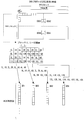
まず、スーパーハイビジョンの映像データの入力(送信)方式として、原画像(フレーム)を、精細度を変えずに16領域の画像に分割して16系統で送信するシングルスキャン方式(図2参照)と、原画像を、該原画像よりも1/16の精細度に落とした16枚の画像(互いに補間するように画素が間引きされた、いわゆる間引き画像)に分割し、n系統で送信するブロックスキャン方式(図2参照)とがある。なお、ブロックスキャン方式では、1系統(1チャンネル)でも1/16の精細度(ピクセルが間引かれた状態)の全体画像を見ることができる。
まず、スーパーハイビジョンの映像データの入力(送信)方式として、原画像(フレーム)を、精細度を変えずに16領域の画像に分割して16系統で送信するシングルスキャン方式(図2参照)と、原画像を、該原画像よりも1/16の精細度に落とした16枚の画像(互いに補間するように画素が間引きされた、いわゆる間引き画像)に分割し、n系統で送信するブロックスキャン方式(図2参照)とがある。なお、ブロックスキャン方式では、1系統(1チャンネル)でも1/16の精細度(ピクセルが間引かれた状態)の全体画像を見ることができる。
実施例1の映像送信装置ITAは、図1に示すように、原画像を16枚に分割し、第1~第16系統の映像データ(コンテンツデータ含む)を生成する映像データ生成回路IGCと、第1~第16系統の映像データの少なくとも1系統に、(分割)送信方式を示す識別データを挿入する識別データ挿入回路IACと、第1~第16系統の映像データそれぞれを差動伝送路(例えば、TMDS)によって送信する出力処理回路OPCとを含む。なお、識別データ挿入回路IACが、第1~第16系統すべての映像データに同一の識別データを挿入するような構成でもよい。
また、実施例1の表示装置DSAは、入力処理回路IPC、識別データ読み取り回路IRCおよびピクセルマッピング回路PMCを含む映像受信装置IRAと、4つの分割表示領域DDA1~DDA4を含む表示パネルDPと、4つの分割表示領域DDA1~DDA4それぞれを駆動するパネル駆動回路PD1~PD4とを含む。なお、表示パネルDPは、例えば、8K4Kパネル(7680×4320画素)であり、4分割の仕方は、上側を左右2つ、下側を左右2つに分割する方式(図1参照)と、上下に分けずに、左右方向に4つに分割する方式とがある。8K4Kパネルについては、後述のように、上側を左右方向に4つ、下側を左右方向に4つに分割する方式(8分割方式)もある。
入力処理回路IPCには、出力処理回路OPCから出力された第1~第16系統の映像データQa1~Qa16が並列(同時)入力される。入力処理回路IPCは、第1~第16系統の映像データに、各ピクセルデータの同期処理、入力映像規格に適したパネル表示を行うためのγカーブ補正、色温度補正および色域変換等を行い、映像データ(Qb1~Qb16)を識別データ読み取り回路IRCに出力する。
識別データ読み取り回路IRCは、第1~第16系統の映像データから識別データを読み取り、これら映像データの送信方式がシングルスキャン方式かブロックスキャン方式かを認識し、映像データQb1~Qb16と送信方式信号TFSとをピクセルマッピング回路PMCに出力する。
ピクセルマッピング回路PMCは、第1~第16系統の映像データを、送信方式信号TFSおよびパネル駆動方式(4分割駆動、図1参照)に応じて並び替え(ピクセルマッピング)、表示制御基板DC1~DC4に出力する。表示制御基板DC1~DC4は、パネル駆動回路PD1~PD4それぞれを制御する。具体的には、ブロックスキャン方式であれば、例えば図3のようにピクセルマッピングを行い、シングルスキャン方式であれば、例えば図4のようにピクセルマッピングを行う。
図5は、第1~第16系統の各系統の入力にHDMI(高精細マルチメディアインターフェース)を用いた場合の映像データの入力状況(1系統分)を示す模式図である。図5に示すように、映像表示期間IDP以外のブランキング期間(垂直ブランキング期間VBPおよび水平ブランキング期間HBP)には、補助データ期間ADPが設けられており、この補助データ期間ADPには、オーディオデータ、フレーム解像度、および色数等の補助データが伝送される。補助データ期間ADPには空き領域(特定の補助データが割り当てられていない領域、リザーブ領域)が設けられているため、例えば、この空き領域に識別データ(フラグ)を挿入すればよい(特開2006-352599および特開2005-184441参照のこと)。
映像送信装置ITAと映像受信装置IRAとの間のHDMI伝送路(1系統分)は、図6に示すように、データチャネル3本(Da-CH0, Da-CH1, Da-CH2)と、クロックチャネル(CK-CH)1本とを含んでおり、補助データはパケット化されてデータチャネル3本を介して送信され、その内容はパケットヘッダーのType値(アドレス)に指定されている。
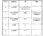
図7は、実施例1の映像データに含まれる補助データの一例である。アドレスは補助データ内のバイトアドレスを示している。まず、補助データの1つとして、送信方式(シングルスキャン方式またはブロックスキャン方式)を示す識別データが含まれ、ブロックスキャン方式の場合(アドレス0の補助データの値が1の場合)は、さらに、1ブロックの水平サイズ(例えば、8画素)を示す補助データと、1ブロックの垂直サイズ(例えば、4ライン)を示す補助データと、入力系統(0~15)を示す補助データとが含まれる。
シングルスキャン方式では、1ブロックの水平サイズおよび垂直サイズは無関係なので0とする。入力系統の補助データはオプションであり、各系統で伝送するピクセルデータの位置を示す。この入力系統の補助データを付加することで、入力系統が正しくなくても(すなわち、16本のケーブルを挿し間違えても)、ピクセルマッピング回路PMCは、正しい位置にピクセルをもっていくことができる。もっとも、ケーブルごとに対応するピクセル位置が決まっているときは不要である(特開2005-18441を参照)。
このように、本実施例によれば、超高精細映像を伝送するための複数の入力方式に対応しうるディスプレイの実現を容易にすることができる。すなわち、ディスプレイの入力部の回路を両方の入力方式で共通化することができ、回路規模とコストを削減することができる。
また、映像レコーダ側は、片方の入力方式で保存しておけばよく、HDD(ハードディスク)などの記録容量を節約できる。また、ユーザーは入力方式を気にしながら、システムセッティングをしなくて済むというメリットもある。
〔実施例2〕
実施例1では、原画像を16枚に分割し、第1~第16系統で伝送しているが、これに限定されない。例えば、図8に示すように、映像送信装置ITAが原画像を4枚に分割し、第1~第4系統(映像データQA1~QA4)で伝送してもよい。この場合、原画像が8K4Kサイズであれば、1系統あたり4K2K画素数が伝送され、送信方式信号TFSがブロックスキャン方式を示している場合、ピクセルマッピング回路PMCは、例えば、図9のようにピクセルマッピングを行う。
実施例1では、原画像を16枚に分割し、第1~第16系統で伝送しているが、これに限定されない。例えば、図8に示すように、映像送信装置ITAが原画像を4枚に分割し、第1~第4系統(映像データQA1~QA4)で伝送してもよい。この場合、原画像が8K4Kサイズであれば、1系統あたり4K2K画素数が伝送され、送信方式信号TFSがブロックスキャン方式を示している場合、ピクセルマッピング回路PMCは、例えば、図9のようにピクセルマッピングを行う。
図10は、実施例2の映像データに含まれる補助データの一例である。図10に示すように、入力系統(0~3)を示す補助データのみならず、入力数(4)を示す補助データを付加してもよい。
〔実施例3〕
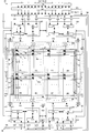
実施例3にかかる液晶表示装置LCDは、フルHD画素数(横1920画素×縦1080画素)の16倍の画素数(8K4K)を有する映像規格(例えば、横7680画素×縦4320画素のスーパーハイビジョン)に対応するものであり、図11に示すように、入力処理回路IPC、識別データ読み取り回路IRC、ピクセルマッピング回路PMC、4つの表示制御基板(タイミングコントローラ基板)DC1~DC4、液晶パネルLCP、4つのゲートドライバGD1~GD4、2つのソースドライバSD1~SD2、4つのCSドライバCD1~CD4、それぞれが異なる商用電源に接続される3つの電源装置(図示せず)、電源コントローラ(図示せず)、バックライトBL、バックライトドライバBLD、およびバックライトコントローラBLCを備える。
実施例3にかかる液晶表示装置LCDは、フルHD画素数(横1920画素×縦1080画素)の16倍の画素数(8K4K)を有する映像規格(例えば、横7680画素×縦4320画素のスーパーハイビジョン)に対応するものであり、図11に示すように、入力処理回路IPC、識別データ読み取り回路IRC、ピクセルマッピング回路PMC、4つの表示制御基板(タイミングコントローラ基板)DC1~DC4、液晶パネルLCP、4つのゲートドライバGD1~GD4、2つのソースドライバSD1~SD2、4つのCSドライバCD1~CD4、それぞれが異なる商用電源に接続される3つの電源装置(図示せず)、電源コントローラ(図示せず)、バックライトBL、バックライトドライバBLD、およびバックライトコントローラBLCを備える。
入力される映像信号Qa1~Qa16には、ブロックスキャンフォーマットであるか、シングルスキャンフォーマットであるかを識別できるような識別データ(補助データ)が付加されており、入力処理回路IPCでは、映像信号Qa1~Qa16に上記の処理を行い、映像信号Qb1~Qb16を識別データ読み取り回路IRCに出力する。
識別データ読み取り回路IRCは、第1~第16系統の映像データから識別データを読み取り、これら映像データの送信方式がシングルスキャン方式かブロックスキャン方式かを認識し、送信方式信号TFSをピクセルマッピング回路PMCに出力する。ピクセルマッピング回路PMCは、送信方式信号TFSに応じてピクセルマッピングを行う。
ここで、表示制御基板DC1は、2つの映像処理回路EP1・EP2および2つのタイミングコントローラTC1・TC2を備え、表示制御基板DC2は、2つの映像処理回路EP3・EP4および2つのタイミングコントローラTC3・TC4を備え、表示制御基板DC3は、2つの映像処理回路EP5・EP6および2つのタイミングコントローラTC5・TC6を備え、表示制御基板DC4は、2つの映像処理回路EP7・EP8および2つのタイミングコントローラTC7・TC8を備える。
ピクセルマッピング回路PMCは、ローカルエリア1(液晶パネルLCPを上下左右に4分割したときの左上領域)の左半分AR1に対応する映像信号(2K2K画素数)を、2本(フルHD画素数の映像信号Qc1・Qc2)に分割して表示制御基板DC1の映像処理回路EP1に出力し、上記ローカルエリア1の右半分AR2に対応する映像信号(2K2K画素数)を、2本(フルHD画素数の映像信号Qc3・Qc4)に分割して表示制御基板DC1の映像処理回路EP2に出力し、ローカルエリア2(液晶パネルLCPを上下左右に4分割したときの右上領域)の左半分AR3に対応する映像信号(2K2K画素数)を、2本(フルHD画素数の映像信号Qc5・Qc6)に分割して表示制御基板DC2の映像処理回路EP3に出力し、上記ローカルエリア2の右半分AR4に対応する映像信号(2K2K画素数)を、2本(フルHD画素数の映像信号Qc7・Qc8)に分割して表示制御基板DC2の映像処理回路EP4に出力し、ローカルエリア3(液晶パネルLCPを上下左右に4分割したときの左下領域)の左半分AR5に対応する映像信号(2K2K画素数)を、2本(フルHD画素数の映像信号Qc9・Qc10)に分割して表示制御基板DC3の映像処理回路EP5に出力し、ローカルエリア3の右半分AR6に対応する映像信号(2K2K画素数)を、2本(フルHD画素数の映像信号Qc11・Qc12)に分割して表示制御基板DC3の映像処理回路EP6に出力し、ローカルエリア4(液晶パネルLCPを上下左右に4分割したときの右下領域)の左半分AR7に対応する映像信号(2K2K画素数)を、2本(フルHD画素数の映像信号Qc13・Qc14)に分割して表示制御基板DC4の映像処理回路EP7に出力し、上記ローカルエリア4の右半分AR8に対応する映像信号(2K2K画素数)を、2本(フルHD画素数の映像信号Qc15・Qc16)に分割して表示制御基板DC4の映像処理回路EP8に出力する。
さらに、ピクセルマッピング回路PMCは、表示制御基板DC1のタイミングコントローラTC1に同期信号SYS(垂直同期信号、水平同期信号、クロック信号、データイネーブル信号等)を出力し、これを受けたタイミングコントローラTC1は、この同期信号SYSを、表示制御基板DC1~DC4に接続された基板間共有線SSLに送信する。
タイミングコントローラTC1は、ピクセルマッピング回路PMCから受けた同期信号SYSを受けて映像処理回路EP1と協働し、映像信号Qc1・Qc2に階調変換処理等の映像処理を行った後に、AR1に対応するソースドライバ基板(図示せず)にソース制御信号SC1を出力し、ゲートドライバGD1のゲートドライバ基板(図示せず)にゲート制御信号GC1を出力し、CSドライバCD1にCS制御信号CC1を出力する。
タイミングコントローラTC2は、タイミングコントローラTC1から基板間共有線SSLを介して送信された同期信号SYSを受けて映像処理回路EP2と協働し、映像信号Qc3・Qc4に上記映像処理を行った後に、AR2に対応するソースドライバ基板(図示せず)にソース制御信号SC2を出力する。
タイミングコントローラTC3は、タイミングコントローラTC1から基板間共有線SSLを介して送信された同期信号SYSを受けて映像処理回路EP3と協働し、映像信号Qc5・Qc6に上記映像処理を行った後に、AR3に対応するソースドライバ基板(図示せず)にソース制御信号SC3を出力する。
タイミングコントローラTC4は、タイミングコントローラTC1から基板間共有線SSLを介して送信された同期信号SYSを受けて映像処理回路EP4と協働し、映像信号Qc7・Qc8に上記映像処理を行った後に、AR4に対応するソースドライバ基板(図示せず)にソース制御信号SC4を出力し、ゲートドライバGD2のゲートドライバ基板(図示せず)にゲート制御信号GC2を出力し、CSドライバCD2にCS制御信号CC2を出力する。
タイミングコントローラTC5は、タイミングコントローラTC1から基板間共有線SSLを介して送信された同期信号SYSを受けて映像処理回路EP5と協働し、映像信号Qc9・Qc10に上記映像処理を行った後に、AR5に対応するソースドライバ基板(図示せず)にソース制御信号SC5を出力し、ゲートドライバGD3のゲートドライバ基板(図示せず)にゲート制御信号GC3を出力し、CSドライバCD3にCS制御信号CC3を出力する。
タイミングコントローラTC6は、タイミングコントローラTC1から基板間共有線SSLを介して送信された同期信号SYSを受けて映像処理回路EP6と協働し、映像信号Qc11・Qc12に上記映像処理を行った後に、AR6に対応するソースドライバ基板(図示せず)にソース制御信号SC6を出力する。
タイミングコントローラTC7は、タイミングコントローラTC1から基板間共有線SSLを介して送信された同期信号SYSを受けて映像処理回路EP7と協働し、映像信号Qc13・Qc14に上記映像処理を行った後に、AR7に対応するソースドライバ基板(図示せず)にソース制御信号SC7を出力する。
タイミングコントローラTC8は、タイミングコントローラTC1から基板間共有線SSLを介して送信された同期信号SYSを受けて映像処理回路EP8と協働し、映像信号Qc15・Qc16に上記映像処理を行った後に、AR8に対応するソースドライバ基板(図示せず)にソース制御信号SC8を出力し、ゲートドライバGD4のゲートドライバ基板(図示せず)にゲート制御信号GC4を出力し、CSドライバCD4にCS制御信号CC4を出力する。
なお、ソース制御信号SC1~SC8には、データ信号、データラッチ信号、ソーススタートパルス、およびソースクロックが含まれ、ゲート制御信号GC1~GC4には、ゲートスタートパルスおよびゲートクロックが含まれる。
表示制御基板DC1~DC4は、基板間で各種信号をやり取りあるいは共有することで、互いの動作を同期させている。具体的には、マスターである表示制御基板DC1が、RDY(準備完了)信号をスレーブの表示制御基板DC2に送り、これを受けた表示制御基板DC2は、準備が完了し次第、RDY信号をスレーブの表示制御基板DC3に送り、これを受けた表示制御基板DC3は、準備が完了し次第、RDY信号をスレーブの表示制御基板DC4に送り、これを受けた表示制御基板DC4は、準備が完了し次第、RDY信号を表示制御基板DC1に返送する。表示制御基板DC1は、RDY信号が返送されたのを受けて、動作開始(SRST)信号を、基板間共有線SSLを介して表示制御基板DC2~DC4に一斉送信する。動作開始(SRST)信号が送信された後には、表示制御基板DC1のタイミングコントローラTC1が、ピクセルマッピング回路PMCから受けた上記同期信号SYSを、基板間共有線SSLを介して、タイミングコントローラTC2~TC8に一斉送信する。
液晶パネルLCPは、アクティブマトリクス基板、液晶層(図示せず)および対向基板(図示せず)を備え、アクティブマトリクス基板には、複数の画素電極(図示せず)、複数のTFT(薄膜トランジスタ、図示せず)、行方向(パネルの長辺に沿う方向)に延伸する走査信号線Ga~Gd、列方向に延伸する複数のデータ信号線Sa~Sd、行方向に延伸する保持容量配線(CS配線)CSa~CSd、および列方向に延伸するCS幹配線Ma~Mhが設けられ、対向基板には、共通電極(図示せず)、カラーフィルタ、およびブラックマトリクス(図示せず)が設けられている。
また、ゲートドライバGD1は、液晶パネルLCPの上半分が有する2つの短辺の一方に沿って設けられ、列方向に並ぶ複数のゲートドライバチップIを含む。垂直ドライバGD2は、液晶パネルLCPの上半分が有する上記2つの短辺の他方に沿って設けられ、列方向に並ぶ複数のゲートドライバチップIを含む。また、ゲートドライバGD3は、液晶パネルLCPの下半分が有する2つの短辺の一方に沿って設けられ、列方向に並ぶ複数のゲートドライバチップIを含む。垂直ドライバGD4は、液晶パネルLCPの下半分が有する上記2つの短辺の他方に沿って設けられ、列方向に並ぶ複数のゲートドライバチップIを含む。そして、パネル上半分に設けられた各走査信号線はゲートドライバGD1・GD2によって駆動され、パネル下半分に設けられた各走査信号線はゲートドライバGD3・GD4によって駆動される。すなわち、1本の走査信号線がその両側に配置された2つのゲートドライバに接続され、これら2つのゲートドライバからこの1つの走査信号線に同一位相の走査(パルス)信号が供給される。こうすれば、走査信号線のCR(時定数)に起因する信号鈍りのばらつき(行方向の位置によって信号鈍りの度合いが変わること)を抑制することができる。
ソースドライバSD1は、液晶パネルLCPの上半分が有する1つの長辺に沿って設けられ、行方向に並ぶ48個のソースドライバチップJ(1つのソースドライバチップの出力端子数は960個)と、図示しない4つのソースドライバ基板を含む(1つのソースドライバ基板には12個のソースドライバチップJが装着される)。一方、ソースドライバSD2は、液晶パネルLCPの下半分が有する1つの長辺に沿って設けられ、行方向に並ぶ48個のソースドライバチップJ(1つのソースドライバチップの出力端子数は960個)と、図示しない4つのソースドライバ基板を含む(1つのソースドライバ基板には12個のソースドライバチップJが装着される)。そして、パネル上半分に設けられた各データ信号線はソースドライバSD1によって駆動され、パネル下半分に設けられた各データ信号線はソースドライバSD2によって駆動される。例えば、データ信号線SaはソースドライバSD1によって駆動され、データ信号線ScはソースドライバSD2によって駆動される。
液晶パネルLCPは、1つの画素列の上半分(第1領域、パネルの上流側)に対応して2本のデータ信号線が設けられるとともに、この画素列の下半分(第2領域、パネルの下流側)に対応して2本のデータ信号線が設けられた、いわゆる上下分割ダブルソース構造(1画素列あたり4本のデータ信号線が設けられ、同時に4本の走査信号線を選択することが可能な構造)を有し、4倍速駆動が可能である。さらに、液晶パネルLCPは、1つの画素に少なくとも2つの画素電極を備えたいわゆるマルチ画素方式であり、1画素内に形成された明領域と暗領域とによって視野角特性を高めることが可能となっている。
なお、パネル上半分に設けられたデータ信号線の数は、少なくとも7680(画素)×3(原色)×2(ダブルソース)=46080本であり、パネル上半分に設けられた走査信号線の数は、少なくとも2160本であり、パネル上半分に設けられた保持容量配線の数は、少なくとも2160本であり、パネル下半分に設けられたデータ信号線の数は、少なくとも46080本であり、パネル下半分に設けられた走査信号線の数は、少なくとも2160本であり、パネル下半分に設けられた保持容量配線の数は、少なくとも2160本である。
以上のように、本データ構造は、原画像をn個(nは2以上の整数)の領域に分割して第1~第n系統で送信する方式を第1方式、原画像を原画像よりも低精細のn枚(nは2以上の整数)の画像に分割して第1~第n系統で送信する方式を第2方式として、原画像の内容を示すコンテンツデータと、送信方式が第1または第2方式であることを示す識別データとを含むものである。
このように、コンテンツデータと送信方式を示す識別データとを含むデータ構造にすることで、両方式に対応しうる映像受信装置の実現を容易にすることができる。
本データ構造では、上記識別データは補助データの1つである構成とすることもできる。
本データ構造では、上記第2方式は、原画像を、それぞれがnの自然数倍の画素を含む複数のブロックに分けるとともにこれらnの自然数倍の画素を第1~第n系統に配分するものであり、第2方式であることを示す識別データを含む場合には、1ブロックのサイズを示すブロックサイズデータも含まれている構成とすることもできる。
本データ構造では、第1~第n系統のいずれに対応するのかを示す系統データも含まれている構成とすることもできる。
本データ構造では、上記n枚の画像それぞれが、高精細度テレビジョン放送の映像規格と同一の画素数を含む構成とすることもできる。
本映像送信装置は、原画像をn個(nは2以上の整数)の領域に分割して第1~第n系統で送信する方式を第1方式、原画像を原画像よりも低精細のn枚(nは2以上の整数)の画像に分割して第1~第n系統で送信する方式を第2方式として、原画像の内容を示すコンテンツデータと、送信方式が第1または第2方式であることを示す識別データとを送信するものである。
本映像送信装置は、第1~第n系統それぞれに差動伝送路が用いられる構成とすることもできる。
本映像受信装置は、上記データ構造を有する映像データを受け付けるものである。
本映像受信装置は、上記識別データに示された送信方式に応じてコンテンツデータを並び替える構成とすることもできる。
本表示装置は、上記映像受信装置を備える。
本映像送信方法は、原画像をn個(nは2以上の整数)の領域に分割して第1~第n系統で送信する方式を第1方式、原画像を原画像よりも低精細のn枚(nは2以上の整数)の画像に分割して第1~第n系統で送信する方式を第2方式として、原画像の内容を示すコンテンツデータと、送信方式が第1または第2方式であることを示す識別データとを送信するものである。
本記録媒体は、上記データ構造を有する映像データが記録された、コンピュータ読み取り可能なものである。
本発明は上記の実施の形態に限定されるものではなく、上記実施の形態を技術常識に基づいて適宜変更したものやそれらを組み合わせて得られるものも本発明の実施の形態に含まれる。
本発明は、例えば、超高精細の液晶表示装置に好適である。
DSA 表示装置
DP 表示パネル
DDA1~DDA4 (表示パネル内の)分割表示領域
ITA 映像送信装置
IRA 映像受信装置
IAC 識別データ挿入回路
IRC 識別データ読み取り回路
PMC ピクセルマッピング回路
TC1~TC8 タイミングコントローラ
DC1~DC4 表示制御基板
LCP 液晶パネル
Pa~Pd 画素
Ga~Gd 走査信号線
Sa~Sd データ信号線
AR1~AR8 (液晶パネル内の)分割表示領域
DP 表示パネル
DDA1~DDA4 (表示パネル内の)分割表示領域
ITA 映像送信装置
IRA 映像受信装置
IAC 識別データ挿入回路
IRC 識別データ読み取り回路
PMC ピクセルマッピング回路
TC1~TC8 タイミングコントローラ
DC1~DC4 表示制御基板
LCP 液晶パネル
Pa~Pd 画素
Ga~Gd 走査信号線
Sa~Sd データ信号線
AR1~AR8 (液晶パネル内の)分割表示領域
Claims (12)
- 原画像をn個(nは2以上の整数)の領域に分割して第1~第n系統で送信する方式を第1方式、原画像を原画像よりも低精細のn枚(nは2以上の整数)の画像に分割して第1~第n系統で送信する方式を第2方式として、
原画像の内容を示すコンテンツデータと、送信方式が第1または第2方式であることを示す識別データとを含むデータ構造。 - 上記識別データは補助データの1つである請求項1記載のデータ構造。
- 上記第2方式は、原画像を、それぞれがnの自然数倍の画素を含む複数のブロックに分けるとともにこれらnの自然数倍の画素を第1~第n系統に配分するものであり、
第2方式であることを示す識別データを含む場合には、1ブロックのサイズを示すブロックサイズデータも含まれている請求項1記載のデータ構造。 - 第1~第n系統のいずれに対応するのかを示す系統データも含まれている請求項1記載のデータ構造。
- 上記n枚の画像それぞれが、高精細度テレビジョン放送の映像規格と同一の画素数である請求項1記載のデータ構造。
- 原画像をn個(nは2以上の整数)の領域に分割して第1~第n系統で送信する方式を第1方式、原画像を原画像よりも低精細のn枚(nは2以上の整数)の画像に分割して第1~第n系統で送信する方式を第2方式として、
原画像の内容を示すコンテンツデータと、送信方式が第1または第2方式であることを示す識別データとを送信する映像送信装置。 - 第1~第n系統それぞれに差動伝送路が用いられる請求項6記載の映像送信装置。
- 請求項1記載のデータ構造を有する映像データを受け付ける映像受信装置。
- 上記識別データに示された送信方式に応じてコンテンツデータを並び替える請求項8記載の映像受信装置。
- 請求項8記載の映像受信装置を備えた表示装置。
- 原画像をn個(nは2以上の整数)の領域に分割して第1~第n系統で送信する方式を第1方式、原画像を原画像よりも低精細のn枚(nは2以上の整数)の画像に分割して第1~第n系統で送信する方式を第2方式として、
原画像の内容を示すコンテンツデータと、送信方式が第1または第2方式であることを示す識別データとを送信する映像送信方法。 - 請求項1記載のデータ構造を有する映像データが記録されたコンピュータ読み取り可能な記録媒体。
Priority Applications (1)
| Application Number | Priority Date | Filing Date | Title |
|---|---|---|---|
| US14/119,206 US20140092301A1 (en) | 2011-05-25 | 2012-05-22 | Data structure, image transmitting apparatus, image receiving apparatus, display apparatus, image transmitting method, and recording medium |
Applications Claiming Priority (2)
| Application Number | Priority Date | Filing Date | Title |
|---|---|---|---|
| JP2011-117387 | 2011-05-25 | ||
| JP2011117387 | 2011-05-25 |
Publications (1)
| Publication Number | Publication Date |
|---|---|
| WO2012161187A1 true WO2012161187A1 (ja) | 2012-11-29 |
Family
ID=47217263
Family Applications (1)
| Application Number | Title | Priority Date | Filing Date |
|---|---|---|---|
| PCT/JP2012/063040 Ceased WO2012161187A1 (ja) | 2011-05-25 | 2012-05-22 | データ構造、映像送信装置、映像受信装置、表示装置、映像送信方法、記録媒体 |
Country Status (2)
| Country | Link |
|---|---|
| US (1) | US20140092301A1 (ja) |
| WO (1) | WO2012161187A1 (ja) |
Families Citing this family (1)
| Publication number | Priority date | Publication date | Assignee | Title |
|---|---|---|---|---|
| US10957233B1 (en) * | 2019-12-19 | 2021-03-23 | Novatek Microelectronics Corp. | Control method for display panel |
Citations (3)
| Publication number | Priority date | Publication date | Assignee | Title |
|---|---|---|---|---|
| JPH07298258A (ja) * | 1994-04-28 | 1995-11-10 | Nippon Telegr & Teleph Corp <Ntt> | 画像符号化復号化方法 |
| JP2001339722A (ja) * | 2000-05-26 | 2001-12-07 | Matsushita Electric Ind Co Ltd | マルチチャネル画像符号化装置、復号化表示装置、符号化方法および復号化表示方法 |
| WO2011027440A1 (ja) * | 2009-09-02 | 2011-03-10 | 株式会社 東芝 | 画像圧縮装置及び画像伸張装置 |
Family Cites Families (2)
| Publication number | Priority date | Publication date | Assignee | Title |
|---|---|---|---|---|
| JP4645638B2 (ja) * | 2007-11-22 | 2011-03-09 | ソニー株式会社 | 信号送信装置、信号送信方法、信号受信装置及び信号受信方法 |
| JP4557016B2 (ja) * | 2007-11-22 | 2010-10-06 | ソニー株式会社 | 信号送信装置 |
-
2012
- 2012-05-22 US US14/119,206 patent/US20140092301A1/en not_active Abandoned
- 2012-05-22 WO PCT/JP2012/063040 patent/WO2012161187A1/ja not_active Ceased
Patent Citations (3)
| Publication number | Priority date | Publication date | Assignee | Title |
|---|---|---|---|---|
| JPH07298258A (ja) * | 1994-04-28 | 1995-11-10 | Nippon Telegr & Teleph Corp <Ntt> | 画像符号化復号化方法 |
| JP2001339722A (ja) * | 2000-05-26 | 2001-12-07 | Matsushita Electric Ind Co Ltd | マルチチャネル画像符号化装置、復号化表示装置、符号化方法および復号化表示方法 |
| WO2011027440A1 (ja) * | 2009-09-02 | 2011-03-10 | 株式会社 東芝 | 画像圧縮装置及び画像伸張装置 |
Also Published As
| Publication number | Publication date |
|---|---|
| US20140092301A1 (en) | 2014-04-03 |
Similar Documents
| Publication | Publication Date | Title |
|---|---|---|
| CN101404151B (zh) | 一种多屏拼接装置和方法 | |
| CN103021378B (zh) | 一种多屏拼接显示装置和方法 | |
| US9019353B2 (en) | 2D/3D switchable image display apparatus and method of displaying 2D and 3D images | |
| KR20140022764A (ko) | 동시 디스플레이를 위한 상이한 차원의 비디오 데이터 스트림들의 결합 | |
| US9607542B2 (en) | Display panel driving method, driving device and display device | |
| CN105141876A (zh) | 视频信号转换方法、视频信号转换装置以及显示系统 | |
| US10482847B2 (en) | Driving method and driving apparatus for display panel, and display device | |
| US20110050850A1 (en) | Video combining device, video display apparatus, and video combining method | |
| US20200143772A1 (en) | Video control device and video wall system using the same and control method for outputting video images to the video wall | |
| WO2012157725A1 (ja) | 液晶表示装置 | |
| WO2004072931A1 (en) | Multi-scanning control process and led displaying device | |
| WO2020199889A1 (zh) | 多视点裸眼立体显示器、显示系统及显示方法 | |
| JP2012128376A (ja) | 表示装置 | |
| US20120050271A1 (en) | Stereoscopic image processing device, method for processing stereoscopic image, and multivision display system | |
| CN204906556U (zh) | 视频信号转换装置以及显示系统 | |
| US20150009408A1 (en) | Video signal transmitter apparatus and receiver apparatus using uncompressed transmission system of video signal | |
| US20120256957A1 (en) | Image processing method of performing scaling operations upon respective data portions for multi-channel transmission and image processing apparatus thereof | |
| US20070262944A1 (en) | Apparatus and method for driving a display panel | |
| WO2012161188A1 (ja) | 映像信号処理装置、液晶表示装置 | |
| WO2012157724A1 (ja) | アレイ基板、表示装置、液晶パネルおよび液晶表示装置 | |
| WO2015096457A1 (zh) | 显示装置以及显示方法 | |
| WO2012157722A1 (ja) | 液晶表示装置 | |
| US9350904B2 (en) | Video signal processing apparatus configured to display a video having a resolution higher than full HD, video display apparatus, and electronic device | |
| CN105549931B (zh) | Usb视频拼接播放系统 | |
| WO2012161187A1 (ja) | データ構造、映像送信装置、映像受信装置、表示装置、映像送信方法、記録媒体 |
Legal Events
| Date | Code | Title | Description |
|---|---|---|---|
| 121 | Ep: the epo has been informed by wipo that ep was designated in this application |
Ref document number: 12789076 Country of ref document: EP Kind code of ref document: A1 |
|
| WWE | Wipo information: entry into national phase |
Ref document number: 14119206 Country of ref document: US |
|
| NENP | Non-entry into the national phase |
Ref country code: DE |
|
| 122 | Ep: pct application non-entry in european phase |
Ref document number: 12789076 Country of ref document: EP Kind code of ref document: A1 |
|
| NENP | Non-entry into the national phase |
Ref country code: JP |